lecture 13 yoda project & discussion of fpgas lecturer: simon winberg
TRANSCRIPT

Lecture 13YODA Project &
Discussion of FPGAs
Lecturer:Simon Winberg
Digital Systems
EEE4084F

Lecture Overview
YODA Project FPGA Families
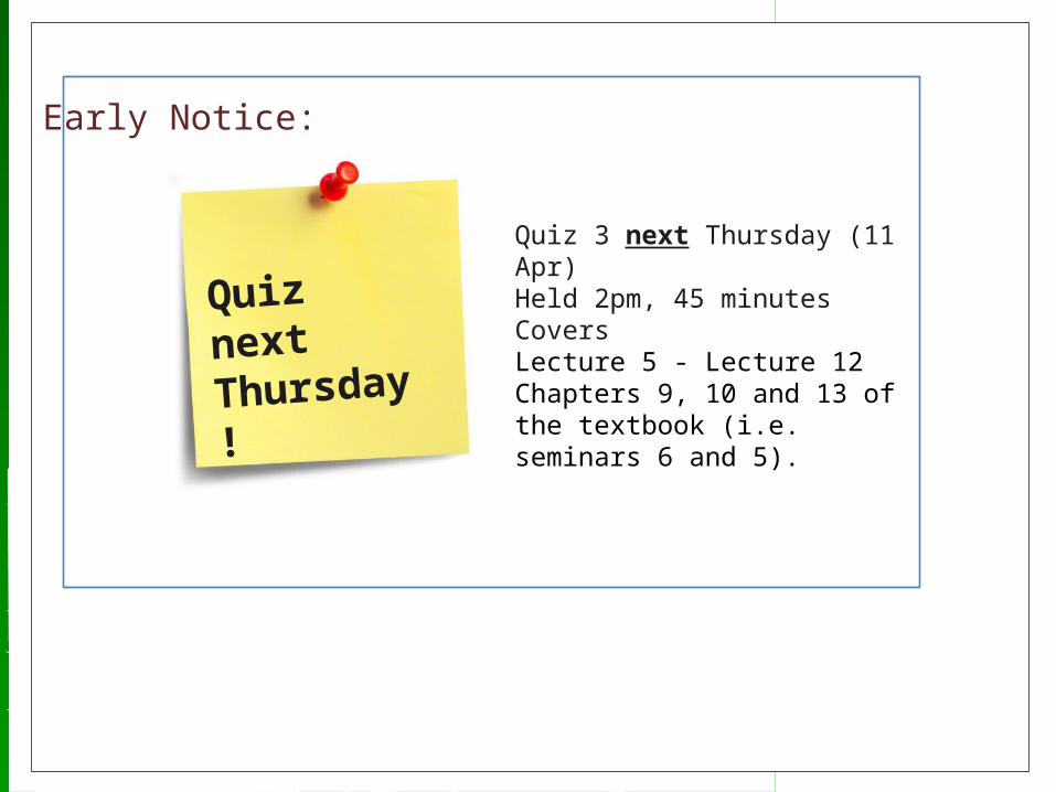
Early Notice:
Quiz nextThursda
y!
Quiz 3 next Thursday (11 Apr)Held 2pm, 45 minutesCoversLecture 5 - Lecture 12Chapters 9, 10 and 13 of the textbook (i.e. seminars 6 and 5).

Reconfigurable ComputingEEE4084F
A SCENARIO…

In the not too distant future,
There was a device…
The Reconfigurable Hardware PlatformMore colloquially, at the startof the mission: “The Doorstop”

The Reconfigurable Hardware PlatformMore colloquially, at the startof the mission: “The Doorstop”
Like most doorstops, this one starts out being alump that is in the way; although it may haveall sorts of potential if you…
… apply your mind, you must!

LCD
Doorstop
MP3player
Jabba says:
I need a MP3 player!
(you may need some additionalexternal items in order to makeuse of the reconfigured system)
Scenario: Reconfigurable platform

MP3player IP phone
The Hutt says:
Now I need an IP
phone!
Yak yak

IP phone Compressor
110111001101
But I (beep beep) need a data stream compressor
(click squeak)
110100

But first patience you must have as this knowledge will berevealed once you are ready…
A “doorstop” for your enlightenment and education…
Your Doorstop
But what is this “doorstop” of which you speak?

Evaluation Kit: Nexys2 or Nexys3Reconfigurable Computing EEE4084F
Getting ready for your “doorstop”…
A brief overview of Reconfigurable Computing operation…

Nexys2:The evaluation board to be usedin the laboratories…
Source: http://www.digilentinc.com/Products/Detail.cfm?NavPath=2,400,789&Prod=NEXYS2

FPGA
Flash 16MByte
SRAM
45 bit memory ADDRESS
BUS
DATA PORT BUS
(USB, JTAG)
32 bit LEDs, PB PIO
43 bit extra IO
16 bit Pmods (4x)
Nexys2:The evaluation board to be usedin the laboratories…
Simplified Model

FPGA
Flash 16MByte
SRAM
45 bit memory ADDRESS
BUS
DATA PORT BUS
(USB, JTAG)
32 bit LEDs, PB PIO
43 bit extra IO
16 bit Pmods (4x)
Nexys2:Simplified Model
BLOCKRAM
Soft Processor
USB DEVICE
USB
Logic
ETHERNET DEVICE
Your own peripheral

Want your own Nexys?
http://www.digilentinc.com/Products/Detail.cfm?NavPath=2,400,897&Prod=NEXYS3
http://www.digilentinc.com/Products/Detail.cfm?NavPath=2,400,789&Prod=NEXYS2
If you want your own Nexys2 or Nexys3 you can order one from the DigilentInc website. These are $99 USD (about R700) each at the academic price. There are plenty to go round for labs. If enough students would like their own Nexys board it’s a good idea to group all into one order to save on the postage costs (the postage is about $50 or R350, only courier options are available).
If you do decide to get your own Nexys, I recommend getting the Nexys3 which has the bigger and more fancy Spartan6 FPGA.

YODA Project:Your Own Digital AcceleratorReconfigurable Computing
Final Hand-in date: 23 May
About YODA

What’s A Digital Application Accelerator?
An add-on card (or reconfigurable co-processor) used to speed up processing for a particular solution
‘Digital’ - comprises digital logic/circuitry to speed-up computation
A GPU could be considered an example (except GPUs often have analogue circuitry as well to connect to monitors)

YODA Example and Scenario
Delta modulator that grabs set of 8 bytes and outputs 1 byte 128 | 200 | 220 | 201 | 201 | 201 | 127 | 108 => 100 = 011001002
Application 1 Flash LEDs according to data send from PC
Application 2 Perform delta compression on data sent from
PC, send compressed steam back to PC
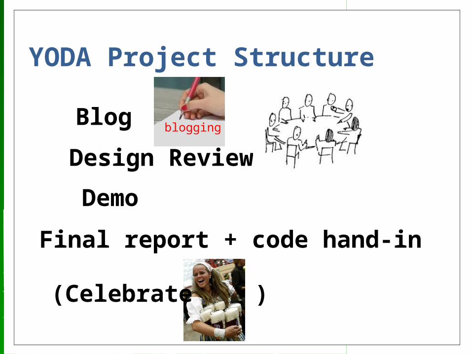
YODA Project Structure
Blog
Design Review
Demo
Final report + code hand-in
blogging
(Celebrate )

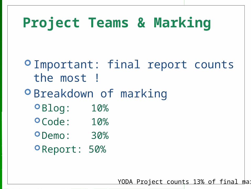
Project Teams & Marking
Projects done as teams of 2 or 3(confirm team of 3 members with
lecturer) Milestone Dates
Blog (due 24 Apr)Design review (to do by 10 May)Demo (21-25 May)Code and final report (25 May)
Project Teams & Marking
Important: final report counts the most !
Breakdown of markingBlog: 10%Code: 10%Demo: 30%Report: 50%
YODA Project counts 13% of final mark
YODA – Purpose
At the end of the course you should have developed an FPGA-based application accelerator for a PC using either a Xilinx-based Digilent Nexys2 or other evaluation board

YODA Design Strategy
In order to trial the reconfigurable aspect, your YODA prototype should support two applicationsApplication 1: something very simple (i.e.,
for testing your setup, send/receive data)Application 2: more sophisticated /
meaningful application (e.g., parallel pattern searches)

YODA Plan
YODAYour Own
Digital Accelerator
YODAForm 1
YODAForm 2
Application 1Supports
Application 2
Supports
Peripherals(e.g. Ethernet
device)
Soft processor
PC(Lab computer)
Windows / Ubuntu
Your VHDL or Verilog HDL
code
Custom logic defined using Public / freely
available VHDL or Verilog HDL
codeAdaptedfrom
Offloadsprocessing to

YODA Demo plan
The demo is just to give me and/or the tutors a conclusive proof that you know what you’re doing, and to explain to us what you’ve done
The demo should be close to the final version, but doesn’t necessarily need to be the final final version.

YODA Report Introduction that recaps your topic Design
High level design Finite State Machine (FSM) documenting your
digital accelerator operation Pseudo code (if relevant) VHDL / Verilog snippets (indicating how your
FSM was implemented) Experimentation and Testing procedure Conclusion and discussion

FPGA FamiliesEEE4084F

The Manufacturers
The ‘Big 2’ (most commonly used)Xilinx – Capital $8.52B, 2984 employeesAltera – Capital $12B, 2555 employees
The others pretty big ones…Actel (Microsemi Corp) – $2B
capitalizations, 2250 employeesLattice Semiconductor Corp – $700M
capitalizations, 708 employees
Sources: “100 Power Tips for FPGA Designers”

About the FPGA Families
XilinxFocusing on highest performance and
highest capacity: Vertex family (e.g. Vertex 6)
Provides lower-cost options with high capacity (e.g. Spartan 6 family)
Range of variations, e.g. low power options, economy (lower capacity) models.

About the FPGA Families
AlteraStratix: higher performance and density
models (e.g. Stratix-V)Arria: mid-range, lower-power, but also
lower performance and denisity compared to Stratix.
Cyclone: lowest cost option, also aimed at low power, cost sensitive and mobile applications

About the FPGA Families
ActelFocuses on providing the lowest power,
and widest range of small packages IGLOO : low power, small footprintSmartFuson : Mixed FPGA and ARM
processorRTAX/RTSX : radiation tolerant and very
high reliability.

About the FPGA Families
LatticeRange of options (low power; high
performance; small package)Own specialized development tools(of these four, this one is the only firms
not in California; they are currently in Oregon)

About the FPGA Families
OthersAchronix – focusing on building the
fastest FPGAs (not necessarily highest capacity)
Tabula – unique FPGA technology ‘SpaceTime’, focusing on highest capacity and memory capabilities

Memory jogger…
Q: What is Xilinx’s highest-capacity FPGA family?
A: Vertex (currently Vertex 6)
Q: Which FPGA manufacturer is focusing on developing the fastest FPGAs?
A: Achronix

Next lecture
RC Basics:Microprocessor-based vs. FPGA-based
solutionsApplication development for FPGA-
based RC systemFPGA and computer board
architecturesPractical techniques
Introduction to Verilog