lecture 13 cmos power...
TRANSCRIPT

EE 471: Transport Phenomena in Solid State DevicesSpring 2018
Lecture 13CMOS Power Dissipation
1
Bryan AcklandDepartment of Electrical and Computer Engineering
Stevens Institute of TechnologyHoboken, NJ 07030
Adapted from Digital Integrated Circuits: A Design Perspective, Rabaey et. al., 2003and Lecture Notes, David Mahoney Harris CMOS VLSI Design

2
• CMOS developed in 1970’s as a low power technology– (almost) no DC current when gate is not switching– no static power dissipation
• CMOS replaces NMOS in 1980’s as dominant digital technology– NMOS designs dissipated about 200µW/gate– Power dissipation no longer an issue!
• CMOS process technology evolves to provide:– more transistors per chip (Moore’s Law)– faster switching speed (few MHz hundreds of MHz)
• 1992 DEC announces Alpha 64-bit microprocessor – triumph of high speed CMOS digital design– first 200MHz processor, 1.7M transistors– 30W power dissipation– Power dissipation is once again an issue!
CMOS – a Low Power Technology

3
• Need to remove heat from high performance chips– max. operating temperature silicon transistors: 150 – 200 °C
• Chip on PC board can dissipate 2-3 watts
• With suitable heatsink, maybe 10 watts
• With forced-air cooling (fans), up to 150W
• With sophisticated liquid cooling, maybe 1000W
Why Power Matters: Package & System Cooling

4
• Today, we see more hand-held battery operated devices
• Unlike CMOS technology, battery technology has seen only modest improvements over last few decades
• Expected battery lifetime increase over the next 5 years: 30 to 40%
Why Power Matters: Battery Size & Weight
“Mobile Computing Environment”, Paradiso et. al. Pervasive Computing, IEEE 2005
5
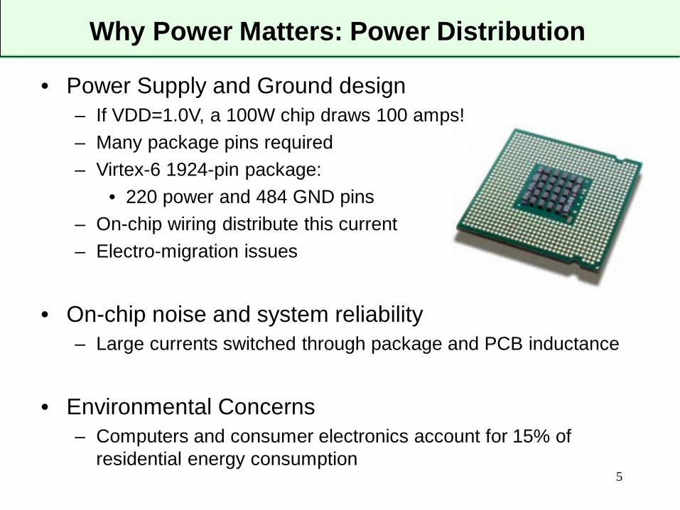
• Power Supply and Ground design– If VDD=1.0V, a 100W chip draws 100 amps!– Many package pins required– Virtex-6 1924-pin package:
• 220 power and 484 GND pins– On-chip wiring distribute this current– Electro-migration issues
• On-chip noise and system reliability– Large currents switched through package and PCB inductance
• Environmental Concerns– Computers and consumer electronics account for 15% of
residential energy consumption
Why Power Matters: Power Distribution

6
• Power is drawn from a voltage source attached to the VDD and GND pins of a chip.
• Instantaneous Power: (watts)
• Energy: (joules)
• Average Power:
Back to Basics: Power & Energy
( ) ( ) ( )P t I t V t=
0
( )T
E P t dt= ∫
avg0
1 ( )TEP P t dt
T T= = ∫

7
• Power Supply:
• Resistor
• Capacitor
– but they do store energy:
Back to Basics: Power in Circuit Elements
( ) ( )VDD DD DDP t I t V=
( ) ( ) ( )2
2RR R
V tP t I t R
R= =
( ) ( ) ( )
( )
0 0
212
0
C
C
V
C
dVE I t V t dt C V t dtdt
C V t dV CV
∞ ∞
= =
= =
∫ ∫
∫
Capacitors don’t dissipate power!
Vc C
V(t)t=0
R

8
• Ptotal = Pdynamic + Pstatic
• Dynamic power: Pdynamic = Pswitching + Pshortcircuit
– Switching load capacitances– Short-circuit current
• Static power: Pstatic = (Isub + Igate + Ijunct + Icontention)VDD– Subthreshold leakage
– Gate leakage
– Junction leakage
– Contention current
Power Dissipation in CMOS

9
• When the gate output rises from GND to VDD:
– Energy stored in capacitor is
– But energy drawn from the supply is
– Half the energy from VDD is dissipated in the pMOS transistor as heat, other half stored in capacitor
• When the gate output falls from VDD to GND– Stored energy in capacitor is dumped to GND– Dissipated as heat in the nMOS transistor
Dynamic Power: Charging a Capacitor
212C L DDE C V=
( )0 0
2
0
DD
VDD DD L DD
V
L DD L DD
dVE I t V dt C V dtdt
C V dV C V
∞ ∞
= =
= =
∫ ∫
∫ independent of size of transistors!
10
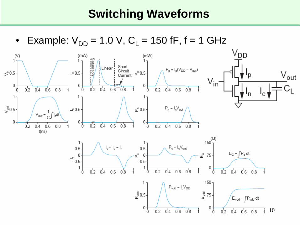
• Example: VDD = 1.0 V, CL = 150 fF, f = 1 GHz
Switching Waveforms

11
Switching Waveforms
Note: Pswitching is independent of drive strength of the nMOS and pMOS transistors
𝑃𝑃𝑠𝑠𝑠𝑠𝑠𝑠𝑠𝑠𝑠𝑠𝑠𝑠𝑠𝑠𝑠𝑠𝑠 =1𝑇𝑇�0
𝑇𝑇𝑖𝑖𝐷𝐷𝐷𝐷(𝑡𝑡)𝑉𝑉𝐷𝐷𝐷𝐷𝑑𝑑𝑡𝑡
=𝑉𝑉𝐷𝐷𝐷𝐷𝑇𝑇
�0
𝑇𝑇𝑖𝑖𝐷𝐷𝐷𝐷(𝑡𝑡) 𝑑𝑑𝑡𝑡
=𝑉𝑉𝐷𝐷𝐷𝐷𝑇𝑇
×𝑡𝑡𝑡𝑡𝑡𝑡𝑡𝑡𝑡𝑡 𝑐𝑐𝑐𝑡𝑡𝑐𝑐𝑐𝑐𝑐𝑐 𝑑𝑑𝑐𝑐𝑡𝑡𝑑𝑑𝑑𝑑𝑓𝑓𝑐𝑐𝑡𝑡𝑓𝑓 𝑝𝑝𝑡𝑡𝑑𝑑𝑐𝑐𝑐𝑐 𝑠𝑠𝑠𝑠𝑝𝑝𝑝𝑝𝑡𝑡𝑠𝑠
𝑖𝑖𝑑𝑑 𝑡𝑡𝑖𝑖𝑓𝑓𝑐𝑐 𝑇𝑇
=𝑉𝑉𝐷𝐷𝐷𝐷𝑇𝑇
× 𝑇𝑇𝑓𝑓𝑠𝑠𝑠𝑠𝐶𝐶𝑉𝑉𝐷𝐷𝐷𝐷
𝑃𝑃𝑠𝑠𝑠𝑠𝑠𝑠𝑠𝑠𝑠𝑠𝑠𝑠𝑠𝑠𝑠𝑠𝑠 = 𝐶𝐶.𝑉𝑉𝐷𝐷𝐷𝐷2.𝑓𝑓𝑠𝑠𝑠𝑠

Activity Factor
• Suppose the system clock frequency = f• Most gates do not switch every clock cycle• Let fsw = αf, where α = activity factor
– α = P0→1 : probability that a signal switches from 0 to 1 in any clock cycle
– If the signal is the system clock, α = 1– If the signal switches once per cycle, α = 0.5– If the signal is random (clocked) data, α = 0.25– Static CMOS logic has (empirically) α ≈ 0.1
• Dynamic power of a circuit: (summing over all the nodes in the circuit)
12
𝑃𝑃𝑠𝑠𝑠𝑠𝑠𝑠𝑠𝑠𝑠𝑠𝑠𝑠𝑠𝑠𝑠𝑠𝑠 = 𝑉𝑉𝐷𝐷𝐷𝐷2.𝑓𝑓.�𝑠𝑠
𝛼𝛼𝑠𝑠 .𝐶𝐶𝑠𝑠

Dynamic Power Example
• 1 billion transistor chip– 50M logic transistors
• Average width: 12 λ• Activity factor = 0.1
– 950M memory transistors• Average width: 4 λ• Activity factor = 0.02
– 65 nm, 1.0V process (λ = 25nm)– C = 1 fF/µm (gate) + 0.8 fF/µm (diffusion)
• Estimate dynamic power consumption @ 1 GHz. Neglect wire capacitance and short-circuit current.
13
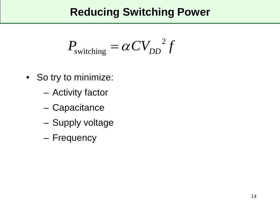
Reducing Switching Power
• So try to minimize:– Activity factor– Capacitance– Supply voltage– Frequency
14
2switching DDP CV fα=

Activity Factor Estimation
• Let Pi = probability (node i = 1)and Pi = (1 – Pi) = probability (node i = 0)
• αi = prob. that node i makes a transition from 0 to 1, so
• αi = Pi • Pi = (1 ─ Pi) • Pi
15Pi
αi
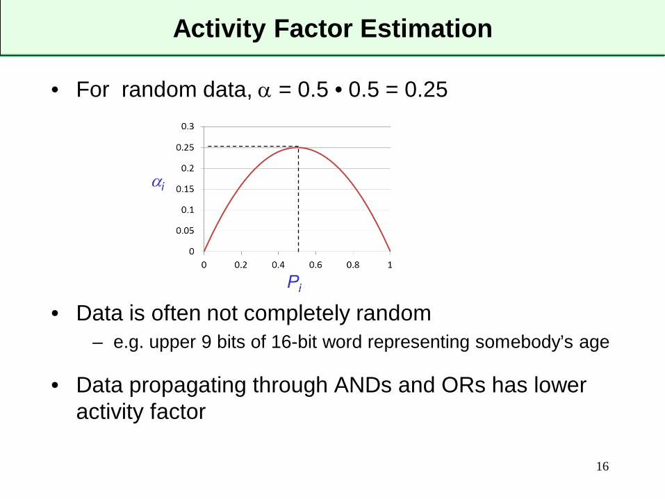
Activity Factor Estimation
• For random data, α = 0.5 • 0.5 = 0.25
• Data is often not completely random– e.g. upper 9 bits of 16-bit word representing somebody’s age
• Data propagating through ANDs and ORs has lower activity factor
16

Example: Switching Probability of NOR2
• For NOR2, PY = PA • PB
• PY = (1 – PY ) = (1 – PA • PB)
• αY = PY • PY
= (PA • PB)•(1 – PA • PB)
• If PA = PB = 0.5, PY = 0.25, αY = 3/16 ≈ 0.1917
A B Y
0 0 1
0 1 0
1 0 0
1 1 0
AB Y

Switching Probabilities (Static Gates)
• Remember αY = PY • PY
18

Example: 4-input AND gate
19
• Assume all inputs have P=0.5
• Which has the lowest power?
ABCD
Y
Y
ABCD
AB C D Y
P=3/4α=3/16
P=3/4α=3/16
P=15/16α=15/256
P=1/16α=15/256
P=1/16α=15/256
P=3/4α=3/16
P=1/4α=3/16
P=7/8α=7/64
P=1/8α=7/64
P=1/16α=15/256
P=15/16α=15/256

Number of Stages vs. Power
20
• Power depends on activity and capacitance at each node
• Generally fewer stages usually mean less power• Compare this to delay
– frequently add stages to improve delay
• Tradeoff between speed and power

Beware of Glitches!
21
• Extra transitions caused by finite propagation delay
Suppose input changesfrom ABCD = “1101” to “0111” ?
Glitching occurs whenever a node makes more transitions than necessary to reach its final value
Glitching can raise the activity factor of a gate to greater than 1!
AB C D Y
n3 n4 n5 n6 n7

Clock Gating
22
• Another way to reduce the activity is to turn off the clock to registers in unused blocks
– Saves clock activity (α = 1)– Eliminates all switching activity in the block– Requires determining if block will be used

Capacitance
23
• Extra capacitance slows response and increases power– Always try to reduce parasitic and wiring capacitance– Good floorplanning to keep high activity communicating gates
close to each other– Drive long wires with inverters or buffers rather than complex gates
• Gate sizing and number of stages– Designing network for minimum delay will
usually result in a high-power network. – Small increase in delay (e.g. by reducing the #
of stages) can give large reduction in power– There are no closed form solutions to
determine gate sizes that minimize power under a delay constraint.
– Can be solved numerically
Delay
Energy

Voltage
24
• Power dissipated in gate is Pav = α.f.CL.VDD2
• Energy per switching event* is Es = Pav/(2.α.f) = (CL.VDD2)/2
– Power & Energy can be significantly reduced by decreasing VDD
• But delay of gate is D = (CL. ∆V)/I
≈ (CL.VDD)/[(β/2).(VDD-Vt)2]
– Decreasing VDD increases delay
• Circuit can be made (almost) arbitrarily low power at the expense of performance – not very useful
* switching event is defined as a transition from 0→1 or 1→0

Energy-Delay Product
25
• Introduce metric energy-delay product (EDP)= (energy per switching event) X (gate delay)
• Minimum EDP at VDD = 3.Vt (for long channel process)
𝐸𝐸𝐸𝐸𝑃𝑃 = 𝐸𝐸𝑠𝑠.𝐸𝐸 =𝑘𝑘.𝐶𝐶𝐿𝐿2.𝑉𝑉𝐷𝐷𝐷𝐷3
𝑉𝑉𝐷𝐷𝐷𝐷 − 𝑉𝑉𝑠𝑠 2
normalized units
VDD
VT = 0.4V

Frequency
26
• Suppose we can do a task in T sec. on one processor
• Can we do it in T/2 sec. on two processors?– if application has sufficient intrinsic parallelism
• How about doing it in T sec. on two processors running at half clock frequency?
• This gives no net power savings.
• But 𝑠𝑠𝑝𝑝𝑐𝑐𝑐𝑐𝑑𝑑 ∝ ⁄(𝑉𝑉𝐷𝐷𝐷𝐷 − 𝑉𝑉𝑇𝑇)2 𝑉𝑉𝐷𝐷𝐷𝐷, so if we reduce clock frequency, we can also reduce 𝑉𝑉𝐷𝐷𝐷𝐷:
Proc. at V volts, f Hz
= P watts
Proc. at V volts, f/2 Hz
= P/2 watts
Proc. at V volts, f/2 Hz
= P/2 watts≡ +
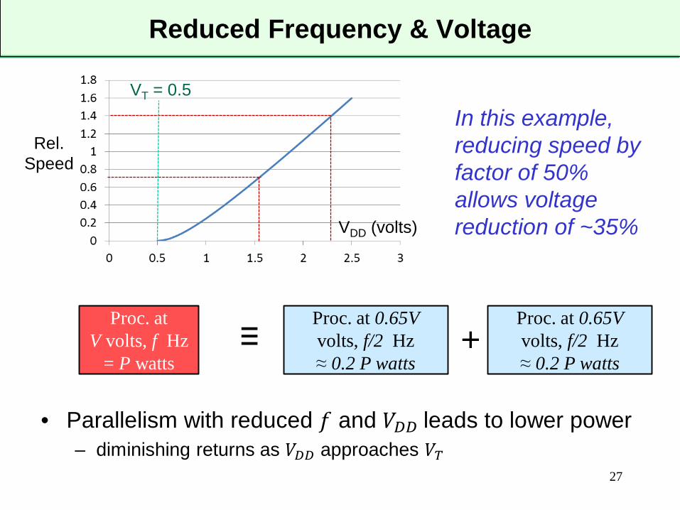
Reduced Frequency & Voltage
27
• Parallelism with reduced 𝑓𝑓 and 𝑉𝑉𝐷𝐷𝐷𝐷 leads to lower power– diminishing returns as 𝑉𝑉𝐷𝐷𝐷𝐷 approaches 𝑉𝑉𝑇𝑇
VDD (volts)
Rel. Speed
VT = 0.5
In this example, reducing speed by factor of 50% allows voltage reduction of ~35%
Proc. at V volts, f Hz
= P watts
Proc. at 0.65V volts, f/2 Hz≈ 0.2 P watts
≡ +Proc. at 0.65V volts, f/2 Hz≈ 0.2 P watts

Dynamic Power Dissipation Example
28
• A NAND2 gate of size (input capacitance) 12C is driving an inverter of size 36C which in turn drives a load of 120C units of capacitance. Assume the inputs A, B are independent and uniformly distributed. What is the dynamic switching power dissipation of this gate if the gate capacitance C of a unit sized transistor is 0.1fF, VDD is 1.0V and the operating frequency is 1GHz?
12012
AB
Y36
Short-Circuit Power
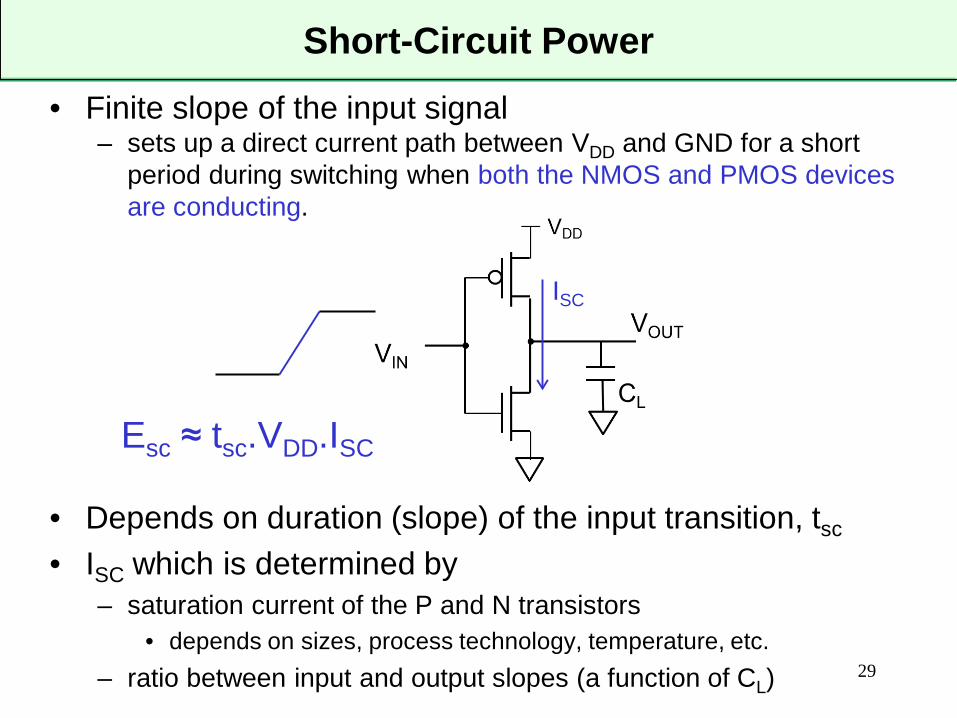
29
• Finite slope of the input signal– sets up a direct current path between VDD and GND for a short
period during switching when both the NMOS and PMOS devices are conducting.
• Depends on duration (slope) of the input transition, tsc
• ISC which is determined by – saturation current of the P and N transistors
• depends on sizes, process technology, temperature, etc.– ratio between input and output slopes (a function of CL)
ISC
Esc ≈ tsc.VDD.ISC

Slope Engineering
30
ISC
Small Capacitive Load
ISC≈0
Large Capacitive Load
• Output fall time significantly shorter than input rise time
• Output “tracks” input as per DC transfer function
• Large ISC when VIN ≈ VSW
• Output fall time significantly longer than input rise time
• Output transition lags input • When VIN = VSW, Vdsp is still
very small, so small ISC
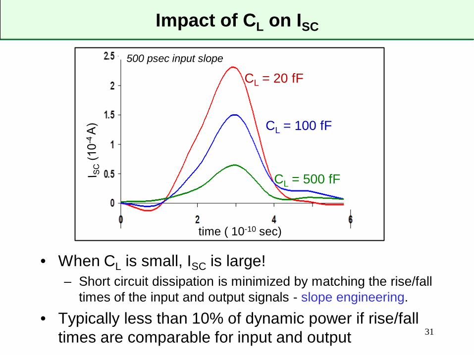
Impact of CL on ISC
• When CL is small, ISC is large!– Short circuit dissipation is minimized by matching the rise/fall
times of the input and output signals - slope engineering.• Typically less than 10% of dynamic power if rise/fall
times are comparable for input and output 31
CL = 20 fF
CL = 100 fF
CL = 500 fF
time ( 10-10 sec)
500 psec input slope

Static Power Dissipation
• Static power is consumed even when chip is quiescent– i.e. powered up but not running
• Leakage consumes power from current passing through normally off devices– sub-threshold current
– gate leakage current
– diode junction leakage current
32

Leakage Sources
• Leakage currents are very small (per transistor basis)– prior to 130 nm, not usually an issue (except in sleep mode of
battery operated devices) – but when multiplied by hundreds of millions of nanometer devices,
can account for as much as 1/3 of active power• All increase exponentially with temperature 33
gate leakage
sub-threshold leakage
junction leakage
Sub-threshold Leakage
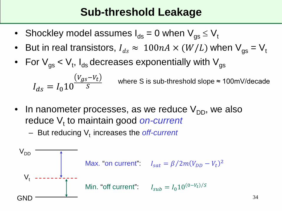
• Shockley model assumes Ids = 0 when Vgs ≤ Vt
• But in real transistors, 𝐼𝐼𝑑𝑑𝑠𝑠 ≈ 100𝑑𝑑𝑛𝑛 × (𝑊𝑊/𝐿𝐿) when Vgs = Vt
• For Vgs < Vt, Ids decreases exponentially with Vgs
• In nanometer processes, as we reduce VDD, we also reduce Vt to maintain good on-current– But reducing Vt increases the off-current
34
𝐼𝐼𝑑𝑑𝑠𝑠 = 𝐼𝐼010𝑉𝑉𝑔𝑔𝑔𝑔−𝑉𝑉𝑡𝑡
𝑆𝑆where S is sub-threshold slope ≈ 100mV/decade
GND
VDD
Vt
Max. “on current”: 𝐼𝐼𝑠𝑠𝑠𝑠𝑠𝑠 = ⁄𝛽𝛽 2𝑓𝑓 𝑉𝑉𝐷𝐷𝐷𝐷 − 𝑉𝑉𝑠𝑠 2
Min. “off current”: 𝐼𝐼𝑠𝑠𝑠𝑠𝑠𝑠 = 𝐼𝐼010 ⁄0−𝑉𝑉𝑡𝑡 𝑆𝑆

• Tradeoff between “on current” (performance) and “off current” (static power dissipation) as we adjust Vt
• Typical values for off-current in 65nm with VDD=1V
Ioff = 100 nA/µm @ Vt = 0.3 VIoff = 10 nA/µm @ Vt = 0.4 VIoff = 1 nA/µm @ Vt = 0.5 V
Sub-threshold Leakage
35
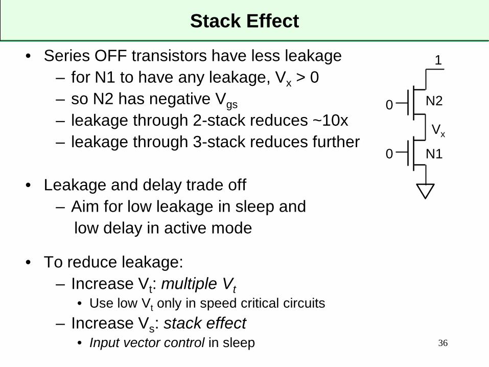
Stack Effect• Series OFF transistors have less leakage
– for N1 to have any leakage, Vx > 0– so N2 has negative Vgs– leakage through 2-stack reduces ~10x– leakage through 3-stack reduces further
• Leakage and delay trade off– Aim for low leakage in sleep and
low delay in active mode
• To reduce leakage:– Increase Vt: multiple Vt
• Use low Vt only in speed critical circuits– Increase Vs: stack effect
• Input vector control in sleep 36
0
0
Vx
1
N2
N1

Gate & Junction Leakage
• Gate leakage extremely strong function of tox and Vgs
– Negligible for older processes
– Approaches sub-threshold leakage at 65 nm
• An order of magnitude less for pMOS than nMOS• Control gate leakage in the process using tox > 10 Å
– High-k gate dielectrics help
– Some processes provide multiple tox
• e.g. thicker oxide for 3.3 V I/O transistors
• Junction leakage usually negligible– becoming little more significant in nanometer processes
• Control gate & junction leakage in circuits by limiting VDD37

Power Gating
• Turn OFF power to blocks when they are idle to save leakage
– Use virtual VDD (VDDV)– Gate outputs to prevent invalid
logic levels to next block
• Voltage drop across sleep transistor degrades performance during normal operation
– Size the transistor wide enough to minimize impact• Switching wide sleep transistor costs dynamic power
– Only justified when circuit sleeps long enough
38
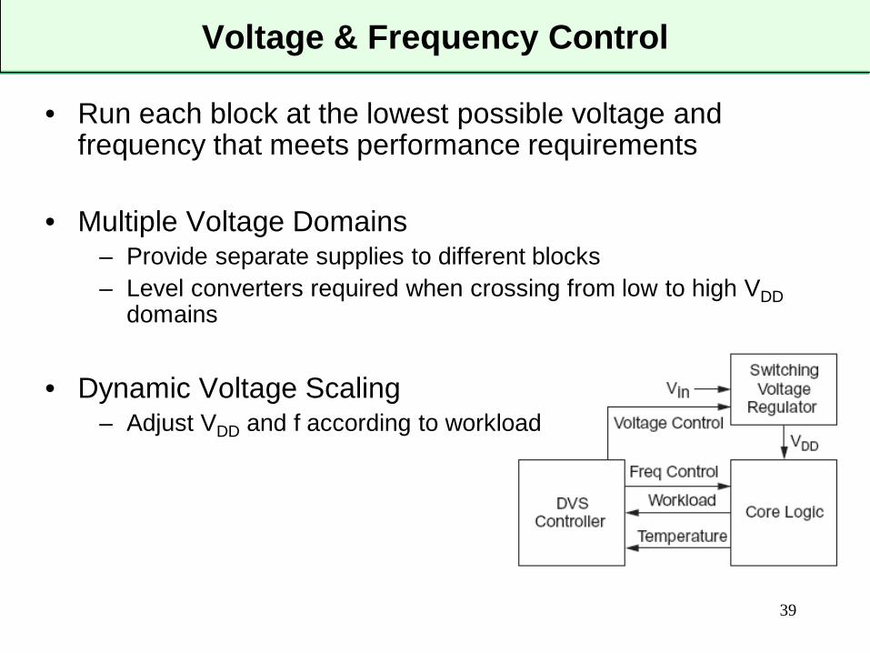
Voltage & Frequency Control
• Run each block at the lowest possible voltage and frequency that meets performance requirements
• Multiple Voltage Domains– Provide separate supplies to different blocks– Level converters required when crossing from low to high VDD
domains
• Dynamic Voltage Scaling– Adjust VDD and f according to workload
39