leakage mechanisms - microwave electronics...
TRANSCRIPT

© 2000, S.K. Streiffer, Argonne National Laboratory, All Rights ReservedNC State
Leakage Mechanisms
Thin films, fully depleted Leakage controlled by combined thermionic /
field emission across the Schottky barrier at the film-electrode interfaces. Film quality effects barrier height, and mobilities of carriers.
Thicker films of interest for higher voltage applications
Poorly understood

© 2000, S.K. Streiffer, Argonne National Laboratory, All Rights ReservedNC State
Much effort has gone into studying the leakage of perovskite-type titanate thin films, including SrTiO3, (Ba,Sr)TiO3, and Pb(Zr,Ti)O3:
J.F. Scott, et al., Proc. of the 1992 IEEE Int. Symp. Appl. Ferro., 356 (1992). T. Makita, et al., Mat. Res. Soc. Symp. Proc. 284, 529 (1993). T. Kuroiwa, et al., Ceramic Transactions 43, 219 (1994). C.S. Hwang, et al., Jpn. J. Appl. Phys. 34, 5178 (1995). M. Kiyotoshi and K. Eguchi, Appl. Phys. Lett. 67, 2468 (1995). R. Waser, in Science and Technology of Electroceramic Thin Films: NATO ASI
Series Vol. 284, ed. O. Auciello and R. Waser (London: Kluwer Academic Publishers, 1995) pp. 223-248.
G. Dietz, et al., J. Appl. Phys. 78, 1 (1995). S. Dey, et al., Jpn. J. Appl. Phys. 34, 3142 (1995). G. Dietz, et al., J. Appl. Phys. 82, 2359 (1997). G. Dietz and R. Waser, Thin Solid Films 299, 53 (1997) S. Zafar, et al., Appl. Phys. Lett. 73, 3533 (1998)

© 2000, S.K. Streiffer, Argonne National Laboratory, All Rights ReservedNC State
Proposed conduction mechanisms for BST thin films:
Fowler-Nordheim tunneling (interface, bulk) Poole-Frenkel effect (bulk) Thermionic emission across Schottky barriers
(interface)
The most favored mechanism:Schottky-barrier limited current flow
© 2000, S.K. Streiffer, Argonne National Laboratory, All Rights ReservedNC State
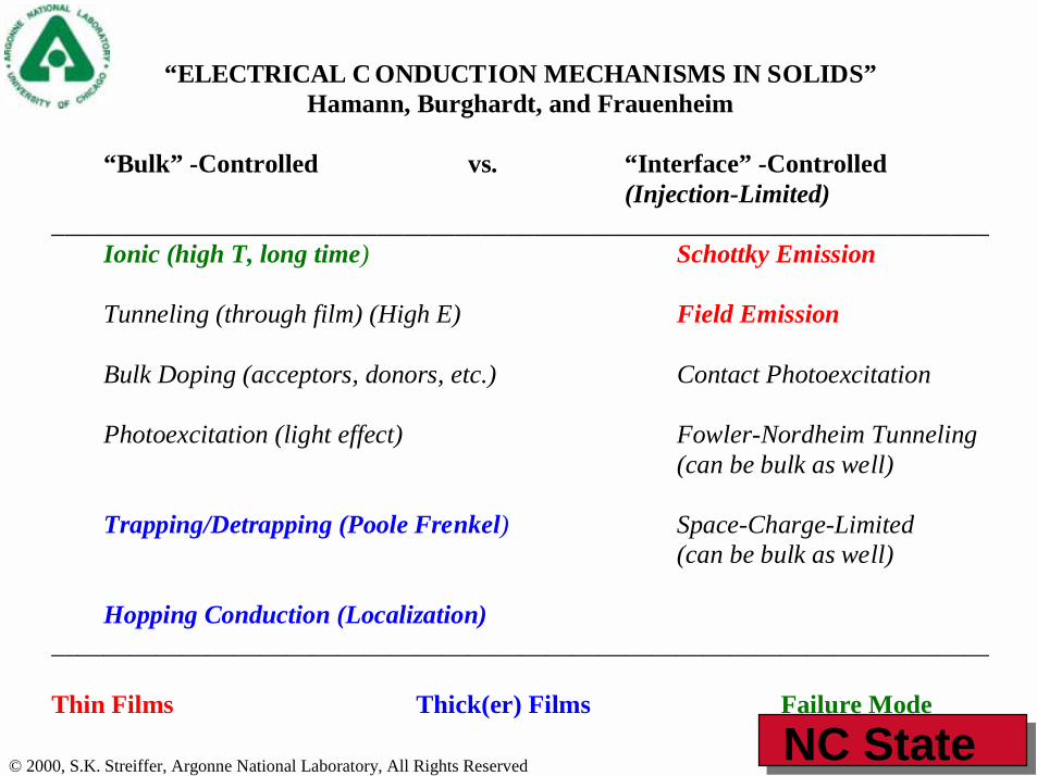
“ELECTRICAL C ONDUCTION MECHANISMS IN SOLIDS”Hamann, Burghardt, and Frauenheim
“Bulk” -Controlled vs. “Interface” -Controlled(Injection-Limited)
________________________________________________________________________Ionic (high T, long time) Schottky Emission
Tunneling (through film) (High E) Field Emission
Bulk Doping (acceptors, donors, etc.) Contact Photoexcitation
Photoexcitation (light effect) Fowler-Nordheim Tunneling(can be bulk as well)
Trapping/Detrapping (Poole Frenkel) Space-Charge-Limited(can be bulk as well)
Hopping Conduction (Localization)________________________________________________________________________
Thin Films Thick(er) Films Failure Mode

© 2000, S.K. Streiffer, Argonne National Laboratory, All Rights ReservedNC State
Lack of complete and careful analyses of leakage in BST thin films
Experimental: Using a ramp or voltage step technique.
– danger of relaxation currents contribution in the analyses
Field and temperature dependencies:– Only field- or temperature-dependent data not sufficient
for understanding the mechanism !
Assumed values for the parameters in the model such as Richardson constant.
Inhomogeneity of Schottky barrier, interfacial roughness, etc.

© 2000, S.K. Streiffer, Argonne National Laboratory, All Rights ReservedNC State
W
²W
WB
metal insulator
xxm
Evac
Ec
EF
Evmetal metal
insulator

© 2000, S.K. Streiffer, Argonne National Laboratory, All Rights ReservedNC State
Leakage vs. A:B Site Ratio
-20
-15
-10
-5
400 500 600 700 800 900 1000 1100
51% Ti @200°C51% Ti @125°C53% Ti @200°C53% Ti @125°C
ln (J
)
E1/2 (V/cm) 1/2
t = 30 nm; T = 125, 150, 175, & 200°C, 0 < V < 3.5V

© 2000, S.K. Streiffer, Argonne National Laboratory, All Rights ReservedNC State
Leakage vs. A:B Site Ratio
-32
-30
-28
-26
-24
-22
-20
-18
-16
-32 -30 -28 -26 -24 -22 -20 -18 -16
Pred
icte
d ln
(J/T
2 )
ln(J/T 2)
51% Ti
-32
-30
-28
-26
-24
-22
-20
-18
-16
-32 -30 -28 -26 -24 -22 -20 -18 -16
Pred
icte
d ln
(J/T
2 )
ln(J/T 2)
53% Ti
ln JT 2
= ln A∗∗ + αE1/ 2 − Wb
kBT

© 2000, S.K. Streiffer, Argonne National Laboratory, All Rights ReservedNC State
Leakage vs. A:B Site Ratio
Ti Content Wb (eV) α A (A/cm2K2)
51% 1.05 0.00085 4.0e-6
51.5 1.28 0.00066 4.2e-3
52 1.44 0.00080 1.2e-2
53 1.17 0.00069 9.1e-5
53.5 0.92 0.00084 3.3e-9
J = A∗∗ T 2 exp αE1/ 2 − WbkBT

© 2000, S.K. Streiffer, Argonne National Laboratory, All Rights ReservedNC State
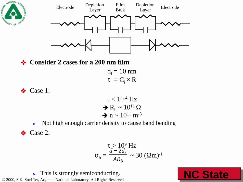
Depletion Widths Issue: What are the depletion lengths?
5 – 10 nm > film thickness (i.e. > 100 nm)
Why is this an issue? Explanation of C-V behavior Affects development directions and ultimate performance predictions
Case for fully depleted film Field dependence in a thickness series:
J(E,T) is almost independent of thickness !!!!Field dropping across entire film thickness
Frequency dependence of permittivity Depletion layer !!!! step frequency dependence
© 2000, S.K. Streiffer, Argonne National Laboratory, All Rights ReservedNC State
Consider 2 cases for a 200 nm filmdi = 10 nmτ = Ci × R
Case 1: τ < 10-4 Hz
!!!! Rb ~ 1011 Ω!!!! n ~ 1011 m-3
Not high enough carrier density to cause band bending Case 2:
τ > 109 Hzσb = ~ 30 (Ωm)-1
This is strongly semiconducting.
Electrode ElectrodeDepletionLayer
DepletionLayer
FilmBulk
d − 2diARb

© 2000, S.K. Streiffer, Argonne National Laboratory, All Rights ReservedNC State
BST Depletion Widths
M. Copel et al., Appl. Phys. Lett. 70, 3227 (1997): W = 70nm for CVD films

© 2000, S.K. Streiffer, Argonne National Laboratory, All Rights ReservedNC State
Failure Modes: Resistance Degradation Change in resistivity of a sample caused by migration of
charged point defects, leading to increased leakage and eventually breakdown
Bulk and single crystals: R. Waser, T. Baiatu, and K.-H. Härdtl, J. Am. Cer. Soc. 73, 1645 (1990); 73, 1654 (1990); J. Am. Cer. Soc. 73, 1663 (1990).
10-5
10-4
10-3
10-2
10-1
10-1 100 101 102 103 104
Cur
rent
Den
sity
(A/c
m2 )
Time (s)
(-) (+)
53.3 at%TiThickness: 40 nmField: 875 kV/cmT = 225°C Resistance degradation in a
polycrystalline (Ba,Sr)TiO3 film, after C. Basceri et al., Ferroelectric Thin Films VI, MRS Symp.Proc. 493 (1998)

© 2000, S.K. Streiffer, Argonne National Laboratory, All Rights ReservedNC State
Resistance Degradation and Lifetime: Thickness Dependence
10-5
10-4
10-3
10-2
10-1
100
101
10-1 100 101 102 103 104 105
Cur
rent
Den
sity
(A/c
m2 )
Time (s)
53.3 at%TiField: 750 kV/cmT = 225°C
24 nm
40 nm80 nm
160 nm
101
102
103
104
105
106
0 20 40 60 80 100
@200°C@225°C@250°C
Mea
sure
d L
ifetim
e, t
d (s)
Thickness (nm)
n=1.85
n=1.48
n=1.47
Observed thickness dependence manifests itself as a decrease in the activation energy with respect to temperature.
Waser: bulk SrTiO3, n ~ 2.5 @ 2 kV/cm, 270°CJ. Am. Ceram. Soc. 73, 1645-1663 (1990).

© 2000, S.K. Streiffer, Argonne National Laboratory, All Rights ReservedNC State
Resistance Degradation and Lifetime: Composition Effect
The measured resistance degradation lifetime at this temperatureand in this field increases as the Ti content is increasedto 52.0 at%Ti, and then decreases with higher at%Ti.
100
101
102
103
104
105
106
400 600 800 1000 1200 1400
51.0 at%Ti (n=10.7)52.0 at%Ti (n=9.5)53.0 at%Ti (n=8.3)53.5 at%Ti (n=8.1)
Mea
sure
d L
ifetim
e, t
d (s)
Field (kV/cm)
T = 225°CThickness: 30 nm

© 2000, S.K. Streiffer, Argonne National Laboratory, All Rights ReservedNC State
Resistance Degradation and Lifetime: Temperature Dependence
Temperature dependence clearly follows an Arrhenius-type behavior:
dt = 0t exp QT (V)kT
101
102
103
104
105
106
1.8 1.9 2 2.1 2.2 2.3M
easu
red
Life
time,
td (s
)
1000/T (1/K)
53.3 at%TiThickness: 40 nmField: 875 kV/cm

© 2000, S.K. Streiffer, Argonne National Laboratory, All Rights ReservedNC State
Resistance Degradation and Lifetime: Voltage/Field Dependence
It is difficult to distinguish the different functional forms ofvoltage/field dependence, given the electric field range investigated:
dt = 0t exp − qVvQ (T)
dt = 0t exp vQ (T)qV
dt = 0t −nV
most conservative
least conservative
© 2000, S.K. Streiffer, Argonne National Laboratory, All Rights ReservedNC State
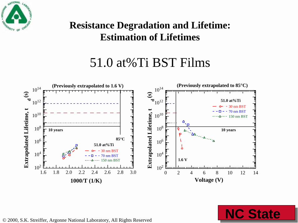
Resistance Degradation and Lifetime: Estimation of Lifetimes
51.0 at%Ti BST Films
102
104
106
108
1010
1012
1014
1.6 1.8 2.0 2.2 2.4 2.6 2.8 3.0
30 nm BST70 nm BST150 nm BST
Ext
rapo
late
d L
ifetim
e, t
d (s)
1000/T (1/K)
85°C
10 years
(Previously extrapolated to 1.6 V)
51.0 at%Ti
102
104
106
108
1010
1012
1014
0 2 4 6 8 10 12 14
30 nm BST70 nm BST150 nm BST
Ext
rapo
late
d L
ifetim
e, t
d (s)
Voltage (V)
1.6 V
10 years
51.0 at%Ti
(Previously extrapolated to 85°C)

© 2000, S.K. Streiffer, Argonne National Laboratory, All Rights ReservedNC State
Resistance Degradation and Lifetime: Modification Of Leakage Behavior
Oxygen vacancies are mobile defects under the given experimentalconditions: electromigration toward cathode.
“Modification of Schotky barrier heights/band structure”(different than bulk resistance degradation mechanism)
Also: Spatial modification of carrier concentrations due to the spatial variation in the oxygen vacancy concentration between the two electrode: change in conductivity of the bulk film.
The accumulation of oxygen vacancies in front of the cathode creates an internal built-in potential at the interface. This space charge modifies the band structure and thus interfacial energy barriers: The difference in barrier heights then appears as an internal bias in the film.

© 2000, S.K. Streiffer, Argonne National Laboratory, All Rights ReservedNC State
Resistance Degradation and Lifetime: Modification Of Leakage Behavior
The differences in barrier heights:
-20
-16
-12
-8
-4
700 800 900 1000 1100 1200
lnJ
(A/c
m2 )
E1/2 (V/cm) 1/2
Fresh
4xts (- deg.)
5xts (- deg.)
53.0 at%TiThickness: 40 nmT = 25°C
(-) Polarity
-20
-16
-12
-8
-4
700 800 900 1000 1100 1200
lnJ
(A/c
m2 )
E1/2 (V/cm) 1/2
Fresh
7xts (+ deg.)
53.0 at%TiThickness: 40 nmT = 25°C
(+) Polarity
4xts: 0.13 eV5xts: 0.21 eV 7xts: 0.22 eV

© 2000, S.K. Streiffer, Argonne National Laboratory, All Rights ReservedNC State
Resistance Degradation and Lifetime: Modification Of Leakage Behavior
The peak shift in C-V: 0.12 V
15
20
25
30
35
40
45
50
55
-5 -4 -3 -2 -1 0 1 2 3 4 5
Fresh4xt
s (-deg.)
C/A
(fF/
µm2 )
Bias (V)
PeakShift: 0.12 V
53.0 at%Tit: 40 nmT = 25°C
0.0000
0.0020
0.0040
0.0060
0.0080
0.0100
-5 -4 -3 -2 -1 0 1 2 3 4 5
tan δδ δδ
Bias (V)

© 2000, S.K. Streiffer, Argonne National Laboratory, All Rights ReservedNC State
Resistance Degradation and Lifetime: Modification Of Leakage Behavior
The peak shift in C-V: 0.20 V
15
20
25
30
35
40
45
50
55
-5 -4 -3 -2 -1 0 1 2 3 4 5
Fresh5xt
s (-deg.)
C/A
(fF/
µm2 )
Bias (V)
PeakShift: 0.20 V
53.0 at%Tit: 40 nmT = 25°C
0.0000
0.0020
0.0040
0.0060
0.0080
0.0100
-5 -4 -3 -2 -1 0 1 2 3 4 5
tan δδ δδ
Bias (V)

© 2000, S.K. Streiffer, Argonne National Laboratory, All Rights ReservedNC State
Resistance Degradation and Lifetime: Modification Of Leakage Behavior
The peak shift in C-V: 0.20 V
15
20
25
30
35
40
45
50
55
-5 -4 -3 -2 -1 0 1 2 3 4 5
Fresh7xt
s (+ deg.)
C/A
(fF/
µm2 )
Bias (V)
PeakShift: 0.20 V
53.0 at%Tit: 40 nmT = 25°C
0.0000
0.0020
0.0040
0.0060
0.0080
0.0100
-5 -4 -3 -2 -1 0 1 2 3 4 5
tan δδ δδ
Bias (V)

© 2000, S.K. Streiffer, Argonne National Laboratory, All Rights ReservedNC State
Resistance Degradation and Lifetime: Modification Of Leakage Behavior
Recovery anneal studies:Negative polarity currents were completely recovered.Positive polarity currents decreased further ?
10-10
10-9
10-8
10-7
10-6
10-5
10-4
10-3
10-2
10-1
0 0.5 1 1.5 2 2.5
Fresh Contact (+)After 11 cycles (+)550°C, 40 min, Air (+)Fresh Contact (-)After 11 Cycles (-)550°C, 40 min, Air (-)
Cur
rent
Den
sity
(A/c
m2 )
V1/2
53.3 at%TiThickness: 40 nmT = 25°C

© 2000, S.K. Streiffer, Argonne National Laboratory, All Rights ReservedNC State
Resistance Degradation and Lifetime: Modification Of Leakage Behavior
C-V behavior indicates that resistance degradation is recoverable.
15
20
25
30
35
40
45
50
55
-4 -2 0 2 4
Fresh ContactAfter 11 CyclesAfter Air Anneal(550°C, 40 min)
C/A
(fF/
µm2 )
Bias (V)
53.3 at%Tit: 40 nmT = 25°C
0.0000
0.0020
0.0040
0.0060
0.0080
0.0100
-4 -2 0 2 4
tan δδ δδ
Bias (V)