latch-up, esd, and other phenomena - アナログ, 半導体, · pdf file ·...
TRANSCRIPT

Application ReportSLYA014A - May 2000
1
Latch-Up, ESD, and Other PhenomenaEilhard Haseloff Standard Linear & Logic
ABSTRACT
The engineer designing an electronic system often needs to know the behavior of itscomponents under operating conditions that are outside those usually described in the datasheets. Thus, although the latch-up effect is no longer a problem with modern CMOS circuits,a closer look at this phenomenon makes it easier for the engineer to assess realistically therisks that may arise under specific – perhaps extreme – operating conditions. Theelectromagnetic compatibility of integrated circuits, as well as their sensitivity and immunityto these effects, plays a significant role. Under particular operating conditions, parasitictransistors in integrated circuits can jeopardize the correct function of a component. Thisapplication report discusses latch-up, electrostatic discharge (ESD), and other phenomena,and their relationships, thereby providing designers information needed to assure thefunctional security of the system, even under extreme operating and environmentalconditions.
Contents
1 Introduction 2. . . . . . . . . . . . . . . . . . . . . . . . . . . . . . . . . . . . . . . . . . . . . . . . . . . . . . . . . . . . . . . . . . . . . . . . .
2 Latch-Up 3. . . . . . . . . . . . . . . . . . . . . . . . . . . . . . . . . . . . . . . . . . . . . . . . . . . . . . . . . . . . . . . . . . . . . . . . . . . . 2.1 Parasitic Thyristors 3. . . . . . . . . . . . . . . . . . . . . . . . . . . . . . . . . . . . . . . . . . . . . . . . . . . . . . . . . . . . . . 2.2 Precautions to Be Taken Against Latch-Up 5. . . . . . . . . . . . . . . . . . . . . . . . . . . . . . . . . . . . . . . . . 2.3 Latch-Up Test 6. . . . . . . . . . . . . . . . . . . . . . . . . . . . . . . . . . . . . . . . . . . . . . . . . . . . . . . . . . . . . . . . . . . 2.4 Pseudolatch-Up 8. . . . . . . . . . . . . . . . . . . . . . . . . . . . . . . . . . . . . . . . . . . . . . . . . . . . . . . . . . . . . . . . . 2.4.1 Pseudolatch-Up With Analog Circuits 8. . . . . . . . . . . . . . . . . . . . . . . . . . . . . . . . . . . . . . . . . . . . . . 2.4.2 Pseudolatch-Up With Bipolar Transistors 9. . . . . . . . . . . . . . . . . . . . . . . . . . . . . . . . . . . . . . . . . . .
3 Electrostatic Discharges 10. . . . . . . . . . . . . . . . . . . . . . . . . . . . . . . . . . . . . . . . . . . . . . . . . . . . . . . . . . . . 3.1 Human-Body Model 10. . . . . . . . . . . . . . . . . . . . . . . . . . . . . . . . . . . . . . . . . . . . . . . . . . . . . . . . . . . . 3.2 Machine Model 12. . . . . . . . . . . . . . . . . . . . . . . . . . . . . . . . . . . . . . . . . . . . . . . . . . . . . . . . . . . . . . . . 3.3 Charged-Device Model 12. . . . . . . . . . . . . . . . . . . . . . . . . . . . . . . . . . . . . . . . . . . . . . . . . . . . . . . . . . 3.4 Charged-Cable Model 14. . . . . . . . . . . . . . . . . . . . . . . . . . . . . . . . . . . . . . . . . . . . . . . . . . . . . . . . . . 3.5 ESD-Protection Circuits 14. . . . . . . . . . . . . . . . . . . . . . . . . . . . . . . . . . . . . . . . . . . . . . . . . . . . . . . . . 3.6 Potentialities and Limitations of Protection Circuits 15. . . . . . . . . . . . . . . . . . . . . . . . . . . . . . . . . . 3.7 External Protection Circuits 17. . . . . . . . . . . . . . . . . . . . . . . . . . . . . . . . . . . . . . . . . . . . . . . . . . . . . .
4 Parasitic Transistors in Integrated Circuits 18. . . . . . . . . . . . . . . . . . . . . . . . . . . . . . . . . . . . . . . . . . . 4.1 Precautions to Protect Analog Circuits 21. . . . . . . . . . . . . . . . . . . . . . . . . . . . . . . . . . . . . . . . . . . . 4.2 High-Frequency Effects 23. . . . . . . . . . . . . . . . . . . . . . . . . . . . . . . . . . . . . . . . . . . . . . . . . . . . . . . . . 4.3 Behavior of Logic Circuits 23. . . . . . . . . . . . . . . . . . . . . . . . . . . . . . . . . . . . . . . . . . . . . . . . . . . . . . .
5 Summary 25. . . . . . . . . . . . . . . . . . . . . . . . . . . . . . . . . . . . . . . . . . . . . . . . . . . . . . . . . . . . . . . . . . . . . . . . . . .
References 26. . . . . . . . . . . . . . . . . . . . . . . . . . . . . . . . . . . . . . . . . . . . . . . . . . . . . . . . . . . . . . . . . . . . . . . . . . . . .

SLYA014A
2 Latch-Up, ESD, and Other Phenomena
List of Figures
1 Parasitic Transistors in a CMOS Circuit 3. . . . . . . . . . . . . . . . . . . . . . . . . . . . . . . . . . . . . . . . . . . . . . . . . . 2 Parasitic Thyristor in a CMOS Circuit 4. . . . . . . . . . . . . . . . . . . . . . . . . . . . . . . . . . . . . . . . . . . . . . . . . . . . 3 Guard Rings in a CMOS Circuit 6. . . . . . . . . . . . . . . . . . . . . . . . . . . . . . . . . . . . . . . . . . . . . . . . . . . . . . . . . 4 Latch-Up Test Circuit 7. . . . . . . . . . . . . . . . . . . . . . . . . . . . . . . . . . . . . . . . . . . . . . . . . . . . . . . . . . . . . . . . . . 5 Simplified Circuit of a Differential Amplifier 8. . . . . . . . . . . . . . . . . . . . . . . . . . . . . . . . . . . . . . . . . . . . . . . 6 Output Characteristics With Load Resistor 9. . . . . . . . . . . . . . . . . . . . . . . . . . . . . . . . . . . . . . . . . . . . . . . 7 Human-Body Model Test Circuit 11. . . . . . . . . . . . . . . . . . . . . . . . . . . . . . . . . . . . . . . . . . . . . . . . . . . . . . . 8 Machine-Model Test Circuit 12. . . . . . . . . . . . . . . . . . . . . . . . . . . . . . . . . . . . . . . . . . . . . . . . . . . . . . . . . . . 9 Equivalent Circuit of Discharge of the Charged-Device Model 13. . . . . . . . . . . . . . . . . . . . . . . . . . . . . . 10 Charged-Device Model Test Setup 13. . . . . . . . . . . . . . . . . . . . . . . . . . . . . . . . . . . . . . . . . . . . . . . . . . . . . 11 ESD-Protection Circuits Using Diodes 14. . . . . . . . . . . . . . . . . . . . . . . . . . . . . . . . . . . . . . . . . . . . . . . . . . 12 Two-Stage ESD-Protection Circuits 15. . . . . . . . . . . . . . . . . . . . . . . . . . . . . . . . . . . . . . . . . . . . . . . . . . . . 13 Protection Circuits for Integrated Circuits 17. . . . . . . . . . . . . . . . . . . . . . . . . . . . . . . . . . . . . . . . . . . . . . . . 14 Protection Circuit for Extreme Requirements 18. . . . . . . . . . . . . . . . . . . . . . . . . . . . . . . . . . . . . . . . . . . . 15 Parasitic Transistors in Bipolar Circuits 19. . . . . . . . . . . . . . . . . . . . . . . . . . . . . . . . . . . . . . . . . . . . . . . . . 16 Input Circuit With Parasitic Transistor 19. . . . . . . . . . . . . . . . . . . . . . . . . . . . . . . . . . . . . . . . . . . . . . . . . . . 17 Parasitic Transistors in CMOS Circuits 20. . . . . . . . . . . . . . . . . . . . . . . . . . . . . . . . . . . . . . . . . . . . . . . . . . 18 Characteristics of Voltage Limiter TL7726 21. . . . . . . . . . . . . . . . . . . . . . . . . . . . . . . . . . . . . . . . . . . . . . . 19 A/D Converter With Limitation of the Input Voltage 22. . . . . . . . . . . . . . . . . . . . . . . . . . . . . . . . . . . . . . . 20 Rectification of High-Frequency Interference Signals 23. . . . . . . . . . . . . . . . . . . . . . . . . . . . . . . . . . . . . 21 Waveforms on an Open-Circuit Line 24. . . . . . . . . . . . . . . . . . . . . . . . . . . . . . . . . . . . . . . . . . . . . . . . . . . .
1 Introduction
When a customer buys an integrated circuit – a gate or an operational amplifier – from asemiconductor manufacturer, it contains considerably more transistors and diodes than arenecessary for the basic function. The additional components, such as the clamping diodes onthe inputs and outputs of logic circuits, are required to ensure reliable operation under particularconditions. These components limit the overshoots and undershoots resulting from linereflections and, thus, reduce signal distortion. Also, protection circuits, which are intended toprotect the component from destruction as a result of electrostatic discharge, are provided.
In addition to these intentionally integrated additional components, an integrated circuit alsocontains a number of transistors and diodes that inevitably result from the construction andmanufacture of the semiconductor circuit. These components are called parasitic transistors anddiodes. Under normal operating conditions, as specified in the data sheets, such parasiticcomponents have no influence on the function of the circuit. However, in particular situations,these parts of the circuit suddenly and unexpectedly can become active, and threaten thecorrect operation of the complete system. Therefore, the development engineer who usesintegrated circuits also must be acquainted with the behavior of parasitic components. Only thencan a circuit be designed with the necessary protective precautions that ensure reliableoperation under required environmental conditions. Parasitic effects are discussed in thefollowing sections to help design engineers understand these phenomena and, if necessary,take suitable precautions to prevent undesirable behavior by the integrated circuit.

SLYA014A
3 Latch-Up, ESD, and Other Phenomena
2 Latch-Up
2.1 Parasitic Thyristors
Isolation of the individual diodes, transistors, and capacitors from each other in an integratedcircuit is achieved by reverse-biased P-N junctions. During the development of the circuit,precautions are taken to ensure that these junctions always are reliably blocking under theconditions that can be expected in the application. However, these P-N junctions form N-P-Nand P-N-P structures with other adjacent junctions. The result of this is parasitic npn or pnptransistors, which can be undesirably activated. The current gain of these transistors is usuallyvery small (ß < 1). As a result, considerable input current is usually necessary to activate thesetransistors. With sensitive analog circuits, interference and other undesirable effects can occur.Also, the transit frequency of these transistors is comparatively low (fT ≈ 1 MHz), which meansthat very short pulses are not able to turn on such transistors.
A typical example for the undesirable interaction between various P-N junctions is thewell-known phenomenon of latch-up, which can occur with CMOS circuits and with BiCMOScircuits that have similar structures: a thyristor formed from parasitic transistors is triggered andgenerates a short-circuit in the circuit. Figure 1 shows the arrangement of the P- and N-dopedregions in a CMOS circuit. For clarity, one structure is shown with incorrect proportions. Thiscircuit represents a simple inverting amplifier.
P+ N+ N+ N+ N+
Rw
P+ P+ P+
NWell
SG D G
SD
VCC
ClampingDiode
N-ChannelTransistor Input Output
P-ChannelTransistor
ClampingDiode
Rs
P Substrate
Figure 1. Parasitic Transistors in a CMOS Circuit

SLYA014A
4 Latch-Up, ESD, and Other Phenomena
In this example, the N-doped regions for source and drain of the N-channel transistor and thecathodes of the clamping diodes have been diffused into a P-doped substrate. The substrate isconnected to the most negative point in the circuit, usually the ground connection (GND). Innormal operation, the N-doped regions have a voltage that is more positive than the groundconnection. In this way, these P-N junctions are blocking. The substrate now forms the base of aparasitic npn transistor, while all N-doped regions – that is, the drain and source of theN-channel transistor and cathode of the clamping diodes – function as emitters. The collectorbelonging to this transistor forms the well in which the complementary P-channel transistor islocated. The latter, with its connections, forms a parasitic pnp transistor. The npn and pnptransistors form a thyristor, as shown in Figure 2. The anode and cathode of this thyristor areconnected to the supply voltage of the integrated circuit, while all other points – inputs andoutputs – function as the gate of the thyristor. As long as the voltages on the latter connectionsstay more positive than the ground connection and more negative than VCC, correct operationoccurs. The base-emitter diodes are blocking.
Anode(VCC)
Rw Output
RsCathode
(GND)
Input
Figure 2. Parasitic Thyristor in a CMOS Circuit
A parasitic thyristor of this kind in an integrated circuit can be triggered in various ways:
• If there is a voltage at the input or output of a circuit that is more positive than the supplyvoltage, or more negative than the ground connection (or, to be precise, more negative thanthe connection to the substrate), current flows into the gate of the thyristor. If the amplitudeand duration of the current are sufficient, the thyristor is triggered. The transit frequency ofthe parasitic transistors is only about 1 MHz. For this reason, overvoltages andundervoltages with durations of only a few nanoseconds, such as result from line reflectionsalong the connections on circuit boards, usually are not able to trigger the thyristor. Withlines of several meters in length and overshoots of correspondingly longer duration, theprobability that the thyristor might be triggered must be taken into account. This applies alsoat the interfaces between a circuit and the outside world; unacceptable overvoltages alsooften occur at this point.
• An electrostatic discharge can trigger the parasitic thyristor. Even if the electrostaticdischarges have a duration of only a few tens of nanoseconds, when this happens, thecomplete chip may be flooded with charge carriers, which then flow away slowly, resulting inthe triggering of the thyristor.

SLYA014A
5 Latch-Up, ESD, and Other Phenomena
• The parasitic thyristor can be triggered by a rapid rise of the supply voltage. This effect oftenwas observed in earlier generations of CMOS circuits.
• Additionally, the thyristor might be triggered by a high supply voltage – far higher than thevalue given in data sheets. In this case, the supply voltage must be increased up to thebreakdown voltage of the transistors. When in breakdown, the current in the parasitictransistors, which should be blocking, increases in an avalanche process, so that activationof the thyristor must be anticipated.
• Also, latch-up can be initiated by ionizing radiation. This is important with components thatoperate close to a source of high-energy radiation.
After the triggering of the thyristor, various reactions can be observed:
• The parasitic thyristor triggers very rapidly and enters a very low-resistance state. Thesource of the supply voltage is short circuited as a result of the circuit that has been affected.A very high current flows, which, in a very short time, leads to destruction of the component.The thyristor can be switched off again only by switching off the supply voltage. Therefore,the recommendation in the literature is that a resistor should be placed in series with thesupply voltage connection to the integrated circuit. If the thyristor does trigger, this resistorlimits the current to a value that no longer poses any danger to the device. If possible, theresistor should limit the current to a value below the holding current of the thyristor such that,after the end of the conditions that led to its being triggered, the thyristor automaticallyswitches off.
• The thyristor triggers in the manner previously described, but, in this case, the thyristor has acomparatively high forward resistance. The result is that only the supply current increases,but this increase usually is quite large. Because of the high power dissipation in the circuit,the component can be damaged. The thyristor usually switches off only after the supplyvoltage has been switched off.
• In some cases, the thyristor has a very high resistance. The high forward resistance limitsthe current to values below the holding current of this thyristor. In this case, the supplycurrent increases. The supply current sinks to normal values when the trigger current at thegate of the thyristor (as a result of an overvoltage at the input or output of the integratedcircuit) is switched off.
2.2 Precautions to Be Taken Against Latch-Up
Semiconductor manufacturers have worked to avoid latch-up of CMOS circuits, and variousprecautions can be implemented. First, the conflicting components can be located as far aspossible from each other. This reduces the current gain of the parasitic transistors, and thetriggering sensitivity of the thyristors is reduced. However, these precautions achieve only limitedsuccess because, for reasons of space and cost, the distance between the conflictingcomponents can be increased only to a certain limit. On the other hand, the continuous processof reduction in the geometries of semiconductor circuits works in the opposite direction.Therefore, other remedies that combat latch-up are necessary, including surrounding the criticalparts of the circuit with guard rings (see Figure 3).

SLYA014A
6 Latch-Up, ESD, and Other Phenomena
P+ N+ N+ P+ N+
Rw
P+ P+ P+
NWell
SG
DG
SD
N-ChannelTransistor
P-ChannelTransistor
Rs
N+N
P Substrate
VCC
Four Guard Rings
Figure 3. Guard Rings in a CMOS Circuit
These guard rings form additional collectors for the parasitic transistors. Such collectors areconnected either to the positive or negative supply-voltage connection of the integrated circuit.These additional collectors are placed considerably closer to the base-emitter region of thetransistor in question than the corresponding connections of the complementary transistor. As aresult, the charge carriers injected into one of the two transistors is diverted largely via theseauxiliary collectors to the positive or negative supply-voltage connection. These precautions donot completely eliminate the questionable thyristor. However, the thyristor’s sensitivity is reducedto such an extent that, under normal operating conditions, there should be little risk of triggeringthe thyristor.
2.3 Latch-Up Test
After designing an integrated circuit, the first samples of the new device are subjected tointensive testing. All relevant parameters are measured – many more than those included in thedata sheets. The latch-up sensitivity of CMOS and BiCMOS circuits also is examined, using thetest circuit shown in Figure 4. The maximum permissible supply voltage is applied to the circuit,then current is injected for a certain duration into each input and output. During this test, thesupply current of the device under test must not rise.

SLYA014A
7 Latch-Up, ESD, and Other Phenomena
VCC
GND
DUT
A
VCC(max)
_
+I
VCC
GND
DUT
A
VCC(max)_
+I
Figure 4. Latch-Up Test Circuit
Measurement conditions are different for various types of circuits. For example, logic circuits ofthe SN54/74 families are subjected to a current of 300 mA to 500 mA for 10 µs at an ambienttemperature of 125°C. These test conditions should comprehend the worst-case operatingconditions. The parasitic transistors in the integrated circuit are bipolar components. The currentgain of such devices increases with temperature and, thus, also the sensitivity of the thyristorthat is to be tested. A test pulse duration of 10 µs should ensure that the questionable thyristor istriggered, if this is possible. As previously mentioned, the transit frequency of the parasitictransistors is very low. Thus, significantly shorter pulses cannot provoke a reaction from thecircuit. The amplitude of the current is used to assess the worst-case conditions under which thecircuit can be operated. Overshoots and undershoots caused by line reflections can – in theory –give rise to currents of up to 100 mA in the clamping diodes (see Section 4.3). At the interfacesto the outside world, under certain circumstances, even higher currents can occur. Additionalinvestigations have shown that, at room temperature, currents of 1 A to 2 A typically are neededto cause latch-up. The test conditions described are potentially destructive, meaning thatdevices tested in this way must not be delivered to customers. The high current density duringthis test might permanently damage the device.
At final test, LinCMOS devices are tested individually for latch-up sensitivity. To avoid damage tothe components, a current of only 100 mA is injected into the device under test. Because analogcomponents, such as operational amplifiers, usually operate in a considerably higher-resistanceenvironment compared to digital circuits, these test conditions are sufficient to cover conditionslikely to occur in practice.
The characteristics of modern CMOS and BiCMOS circuits described here meet practically allthe requirements, with respect to insensitivity to latch-up, that are likely to occur in practice. Onlyin a very few cases would the development engineer need to take additional precautions.
SLYA014A
8 Latch-Up, ESD, and Other Phenomena
2.4 Pseudolatch-Up
In addition to the essential meaning of latch-up, as described previously, this term also is usedcommonly for a number of other phenomena, even though, in such cases, latch-up in itsclassical sense is not involved. Because, in certain applications, effects of the other phenomenaalso can cause serious problems, they are discussed in more detail in the following sections.
2.4.1 Pseudolatch-Up With Analog Circuits
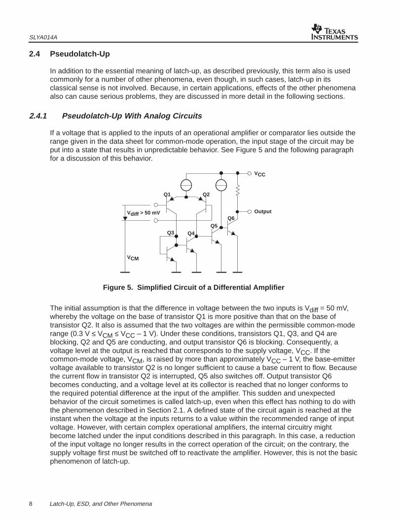
If a voltage that is applied to the inputs of an operational amplifier or comparator lies outside therange given in the data sheet for common-mode operation, the input stage of the circuit may beput into a state that results in unpredictable behavior. See Figure 5 and the following paragraphfor a discussion of this behavior.
Vdiff > 50 mV
VCM
Q1 Q2
Q3 Q4Q5
Q6
VCC
Output
Figure 5. Simplified Circuit of a Differential Amplifier
The initial assumption is that the difference in voltage between the two inputs is Vdiff = 50 mV,whereby the voltage on the base of transistor Q1 is more positive than that on the base oftransistor Q2. It also is assumed that the two voltages are within the permissible common-moderange (0.3 V ≤ VCM ≤ VCC – 1 V). Under these conditions, transistors Q1, Q3, and Q4 areblocking, Q2 and Q5 are conducting, and output transistor Q6 is blocking. Consequently, avoltage level at the output is reached that corresponds to the supply voltage, VCC. If thecommon-mode voltage, VCM, is raised by more than approximately VCC – 1 V, the base-emittervoltage available to transistor Q2 is no longer sufficient to cause a base current to flow. Becausethe current flow in transistor Q2 is interrupted, Q5 also switches off. Output transistor Q6becomes conducting, and a voltage level at its collector is reached that no longer conforms tothe required potential difference at the input of the amplifier. This sudden and unexpectedbehavior of the circuit sometimes is called latch-up, even when this effect has nothing to do withthe phenomenon described in Section 2.1. A defined state of the circuit again is reached at theinstant when the voltage at the inputs returns to a value within the recommended range of inputvoltage. However, with certain complex operational amplifiers, the internal circuitry mightbecome latched under the input conditions described in this paragraph. In this case, a reductionof the input voltage no longer results in the correct operation of the circuit; on the contrary, thesupply voltage first must be switched off to reactivate the amplifier. However, this is not the basicphenomenon of latch-up.

SLYA014A
9 Latch-Up, ESD, and Other Phenomena
2.4.2 Pseudolatch-Up With Bipolar Transistors
Another phenomenon, also called latch-up, occurs with bipolar transistors, particularly withoutput transistors carrying high currents. Figure 6 shows the output characteristics of a bipolartransistor in which the load resistor also is represented. The data sheet for the transistorincludes, among other characteristics, the maximum collector current IC(max) and the breakdownvoltage VCEO of the transistor. These two figures can be assumed to define the limits of thepermissible safe operating area of the transistor.
Latch-UpDuringTurn Off
OperatingPointOn
OperatingPoint
Off
VCEOVCE
IC
IC(max)
LoadResistance
Figure 6. Output Characteristics With Load Resistor
A detailed analysis of the breakdown characteristics of the transistor reveals that, when thetransistor is in breakdown, the breakdown voltage decreases with increasing collector current. Ifa low resistance is drawn in on the diagram, this intersects the corresponding outputcharacteristics, not only at the desired on and off points, but also at a third intersection of thebreakdown characteristics with the load resistance. This is not critical when the transistor isswitched on fast, although, in this case, the breakdown characteristics are exceeded briefly.During this transition, the transistor acquires an increasingly low resistance; therefore, theworking on point is defined reliably. The behavior is very different when the transistor is switchedoff because it travels along the load resistance line in the direction of off. During this journey, thetransistor intersects the breakdown characteristics as it becomes increasingly resistive. At thispoint, the transistor hangs up: the term commonly used is, again, latch-up. A considerablecollector current flows while there is a high collector-emitter voltage. The result is high powerdissipation which, in turn, causes a high chip temperature and results in accelerated aging (andeven destruction) of the component.

SLYA014A
10 Latch-Up, ESD, and Other Phenomena
It often is difficult to detect this situation with commonly used measurement techniques. Ifcontact is made to a point connected to the collector using the test probe of a voltmeter, or withthe probe of an oscilloscope, which usually has a much lower capacitance, the effect mentionedabove no longer can be observed. When there is capacitive loading, the switch-off curve nolonger is a straight-line resistance characteristic but, instead, is a hyperbola. The capacitance atthe output first prevents a rise of the collector voltage, while the collector current already isfalling. As a result, the critical point is avoided.
This kind of latch-up can be avoided effectively only by choosing transistors that have sufficientreserve in the breakdown region. Texas Instruments frequently specifies in data sheets ofinterface circuits a latch-up-free region in which the output transistor can be operated withoutdanger to the device. For example, with the power drivers in the SN75471 family, the data sheetgives a maximum collector voltage in a blocking state (off-state output voltage) of VO = 70 V.This value corresponds approximately to the voltage VCEO in Figure 6. Because of the behaviorin breakdown of the transistor described above, latch-up-free operation is specified only with anoutput voltage of VCE(max) = 55 V and a collector current of IC(max) = 300 mA.
3 Electrostatic Discharges
Electrostatic discharges constitute a danger for integrated circuits that never should beunderestimated1. Electrostatic charging can occur as a result of friction, as well as for otherreasons. When two nonconducting materials rub together, then are separated, oppositeelectrostatic charges remain on both. These charges attempt to equalize each other. A commonexample of the generation of such charges is when one walks with well-insulated shoes on acarpet that is electrically nonconducting, causing the body to become charged. If a conductingobject is touched, for example, a water pipe or a piece of equipment connected to a ground line,the body is discharged. The energy stored in the human body is injected into the object that istouched, and is converted primarily into heat. The power dissipation that arises in such casescan destroy sensitive electronic circuits.
Even though the semiconductor industry has increased efforts to protect components againstdestruction as a result of electrostatic discharges, usually it is not possible to provide adequateprotection in every conceivable situation. Test circuits have been developed to test sensitivity toelectrostatic discharges by simulating various scenarios. These test circuits are analyzed inmore detail in the following paragraphs. These should provide the design engineer with insightinto the reliability of these tests and the effectiveness of the individual protection circuits,providing the criteria to decide, in individual cases, whether additional precautions arenecessary.
3.1 Human-Body Model
The human-body model is described in MIL-STD-883B. The test is a simulation, in which theenergy stored in a human body is discharged into an integrated circuit. The body is charged as aresult of friction, for example. Figure 7 shows the test circuit. In this circuit, a capacitor(C = 100 pF) is charged through a high-value resistor to ±2000 V, then discharged through a1.5-kΩ resistor into the device under test.

SLYA014A
11 Latch-Up, ESD, and Other Phenomena
100 MΩ
±2 kV
1.5 kΩDUT
100 pF
Figure 7. Human-Body Model Test Circuit
The 100-pF capacitor simulates the capacitance of the human body. However, the actualcapacitance of the human body is between 150 pF and 500 pF, depending on size and contactarea (shoe size). Also, the 1.5-kΩ value of the discharge resistor must be considered. Theinternal resistance of the human body ranges from a few kilohms to a few hundred kilohms,depending on various factors, which include the humidity of the skin. However, if the dischargetakes place through a metallic object, such as a screwdriver, the discharge resistor can beassumed to be a few tens of ohms. For these reasons, the corresponding Standard IEC 802-2prescribes a test circuit with a capacitance of 150 pF which, in practice, is more realistic and alower value of discharge resistor (R = 330 Ω). This standard is, however, concerned with a testspecification for equipment that is not directly applicable to integrated circuits. Using a value of2000 V also is questionable because, when a discharge causes a tingling in the tips of thefingers, the body has been charged to at least 4000 V.
The energy of about 0.4 µWs that must be dissipated in the actual protection circuit iscomparatively small. The major part of the energy stored in the capacitor is converted into heatin the discharge resistor. A considerably more-important parameter in the test, according to thismethod, is the rise time of the current during the discharge. Standard IEC 802-2 prescribes arise time of about 0.7 ns at the actual location of the discharge. This value is of interest because,with a fast discharge, at the first instant only a small part of the protection circuit conducts. Onlyduring the subsequent phase (a matter of nanoseconds) does the current spread over thecomplete conducting region of the protection circuit. Therefore, during the first moments of thedischarge, the danger of a partial overload of the protection circuit exists. A similar effect can beobserved with thyristors and triacs. With such components, the rate of current rise aftertriggering must be limited because, at first, only a small area of the semiconductor near thetrigger electrode is conducting. A high current density can result in the destruction of thecomponent. This effect is, however, in many cases responsible for the fact that, even withdischarges from considerably higher voltages, the destruction of the circuit does not necessarilyoccur. The point at which the discharge occurs usually is not at the connections to the integratedcircuit, but, instead, to the cabinet of the equipment or to the contact of a plug. Between thispoint and the endangered integrated circuit there is a length of conductor that has significantinductance. This inductance slows the rate of rise of the current, and helps ensure that thedischarge current is spread evenly over the complete protection circuit.

SLYA014A
12 Latch-Up, ESD, and Other Phenomena
3.2 Machine Model
The test using the machine model simulates the situation in machinery or other equipment thatcontains electronic components or modules. The casing of such equipment is constructedlargely of metal, but often contains plastic bearings or other parts having a wide variety ofshapes and sizes. When individual parts of the machine are in motion, these plastic bearingscan generate electrostatic charges. Figure 8 shows the test circuit. In this test, aC = 200-pF capacitor is charged to ±500 V, then discharged, without a series resistor, into thedevice under test.
100 MΩ
±500 V
DUT
200 pF
>500 nH
Figure 8. Machine-Model Test Circuit
Because the charged metal parts have a very low electrical resistance in this test circuit, noseries resistor is used to limit the current. Therefore, the peak current in the device under test issignificantly higher than in the previously described human-body test circuit. Whereas, in thehuman-body test circuit, extremely short rise times are required, as a result of the extremely lowinductance of the construction used, considerably higher inductances of 500 nH are specified inthe discharge circuit of the machine model. As a result, the rise time of the current and,consequently, its amplitude, are limited. Therefore, the problem of the partial overload of theprotection circuit of the device under test is reduced significantly. The energy of 4 µWs to bedissipated is considerably higher than in the machine-model test.
Because of the high energy used in this test, integrated circuits usually cannot be tested withvoltages of 500 V without damaging the device under test. As a guideline, assume thatcomponents that survive, without damage, the human-body model test with a voltage of up to2000 V, also are not damaged by a machine-model test using voltages of up to ±200 V.
3.3 Charged-Device Model
Despite the informative tests conducted according to the methods described in the previoussections, in practice, damage due to electrostatic discharges also can occur during theprocessing of integrated circuits. It has not been possible to reproduce the profile of failuresobserved during processing by using normal test equipment. Intensive investigations show thatelectrostatic charging, and consequent discharging, of the device are responsible for thedamage. Charging occurs when the integrated circuit slides along plastic transport rails beforebeing inserted into circuit boards, and the discharge occurs when the component lands on thecircuit board. Similarly, damage to the component can occur after it has been tested, when itslides from the test station onto the transport rail, and is damaged by the electrostatic chargingthat occurs. During testing, the integrated circuit was without fault, but it was damagedimmediately afterward. Because the device package is small, the capacitances are only a fewpicofarads, but the inductances also are extremely low (see Figure 9).

SLYA014A
13 Latch-Up, ESD, and Other Phenomena
25 ΩDUT
5 pF
10 nH
Figure 9. Equivalent Circuit of Discharge of the Charged-Device Model
Therefore, in this case, still shorter rise times (<200 ps) of the current can be expected. Becausethe protection circuit is only partially conducting, damage to the circuit can result. The simplifiedtest setup is shown in Figure 10.
Ground Plane
100 MΩChargeProbe
DischargeProbe
High-VoltagePower Supply
Figure 10. Charged-Device Model Test Setup
The device under test is placed on its back on a metal plate. In this way, the largest possiblecapacitance of the circuit to the environment is attained. The circuit is charged with a moveablecharging test probe and discharged with a second test probe.
Investigations have shown that integrated circuits in this test that survive charging up to 1000 Vand subsequent discharging without damage, can be processed without problems in assemblymachinery if the usual precautions to prevent electrostatic charging are taken. There is nocorrelation between the results of the human-body and charged-device model tests.Components that survive the human-body model test without damage do not necessarily behavein the same way in a charged-device test. Conversely, a successful charged-device model testgives no indication of results when a component is tested according to the human-body model.

SLYA014A
14 Latch-Up, ESD, and Other Phenomena
3.4 Charged-Cable Model
The three test methods discussed previously have their justifications, but they do not cover allsituations that might arise. A typical problem that occurs with the use of electronic equipment isrelated to inserting connectors attached to cables. If a user walks on a nonconducting floor withthe plug on the end of a 10-m cable in their hand, the person’s body and the cable becomecharged. When the plug is inserted in the socket of a piece of equipment, the capacitance of thecable is discharged. The capacitance of a 10-m cable is about 1000 pF, producing a chargingvoltage of up to 1000 V. The 500 µWs of energy, which must be tolerated by the integratedcircuit, is many times larger than in the tests described previously. The discharge current, whichis determined by the line impedance of the cable (typically 100 Ω), is about 10 A. This currentflows for a time corresponding to two signal-propagation times, namely, 100 ns. However,because of the comparatively high inductances of the connector and the line connected to itwithin the equipment in question, no exceptionally steep current-pulse edges arise. The problemof the partial conduction of the protection circuits is, to a large extent, eliminated. Therefore, it ispossible to integrate protection circuits that survive such conditions without damage. Thedifferential line driver and receiver interface device SN75LBC184 is a good example of a designthat protects against damage due to electrostatic discharges.
3.5 ESD-Protection Circuits
ESD-protection circuits were first integrated into CMOS devices. The thin and, therefore, veryvulnerable gate oxide of the MOS transistor makes protection against destruction as a result ofelectrostatic discharges essential. The protective precaution that was taken initially, and which isstill the best method, is the integration of clamping diodes, which limit the dangerous voltagesand conduct excess currents into regions of the circuit that are safe. The safe regions consistprimarily of the supply-voltage connections. In the simplest case, the protection circuits consistof diodes that are oriented to be blocking in normal operation, and are situated between theconnection to the component to be protected and the supply voltage lines (see Figure 11).
D3
D4D2
D1
VCC
GND
OutputInput
Figure 11. ESD-Protection Circuits Using Diodes

SLYA014A
15 Latch-Up, ESD, and Other Phenomena
To tolerate even higher energy levels, and to protect the more sensitive parts of a circuit,two-stage protection circuits frequently are used at the inputs (see Figure 12). With thisarrangement, the so-called coarse protection should conduct away the higher energy levels. Inthe example shown, the protective circuit against negative voltages consists of diode D1.Positive voltages are first limited by transistor Q1, which begins to conduct as soon as the inputvoltage (Vin > Vdd + 0.7 V) allows current to flow through resistor R1. If the input voltageincreases further, at about 22 V to 26 V, the thick-oxide MOS field-effect transistor Q2 conducts.Q2 provides additional base current to the base of transistor Q1. In this way, the energy in theinterfering pulse is conducted away reliably. The fine protection circuitry, which should protectthe next device (primarily the gate oxide of the transistors) from excessive voltages, consists ofresistor R2 and Zener diode D3.
R1
D1 D2 D3
Input
GND
R2
Vdd
Q1
Q2
To the Circuitto Be Protected
Figure 12. Two-Stage ESD-Protection Circuits
It is not practical to show all kinds of ESD-protection circuits that have been developed for everyconceivable circuit configuration. The design of these parts of the circuit depends primarily onthe application in which a device is used. Operational amplifiers that have, among otherfeatures, very high-resistance input circuits, use different protective circuits than, for example,interface devices for data-communications systems. In such interfaces, robustness of the deviceis an important characteristic.
3.6 Potentialities and Limitations of Protection Circuits
During design of the circuitry intended to protect an integrated circuit against destruction as aresult of electrostatic discharges, the engineer must consider a number of conflictingrequirements. The rate of thermal conduction in silicon is only 1 µm/µs. Therefore, the protectioncircuit must, at first, be able to withstand the total energy. Only later is the generated heatconducted to the surrounding circuit. By using data based on the charged-cable model, theapproximate area necessary for a protection circuit that can withstand this stress should becalculated.
SLYA014A
16 Latch-Up, ESD, and Other Phenomena
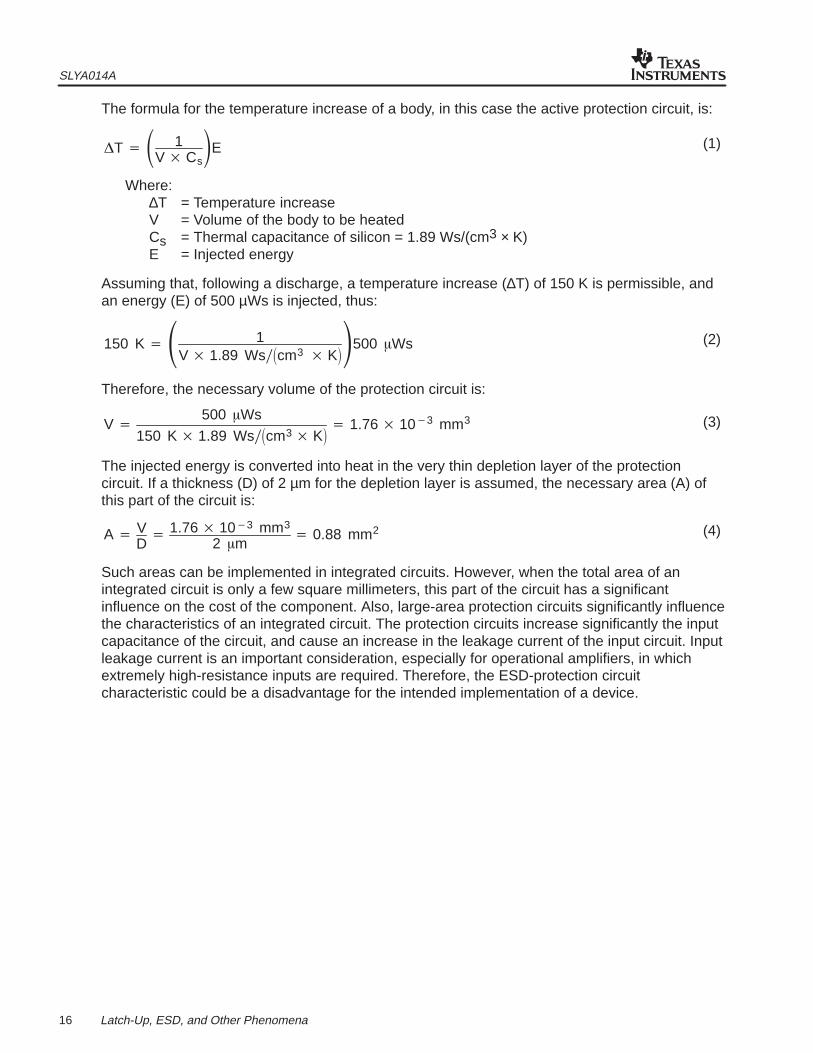
The formula for the temperature increase of a body, in this case the active protection circuit, is:
T 1V Cs
EWhere:
∆T = Temperature increaseV = Volume of the body to be heatedCs = Thermal capacitance of silicon = 1.89 Ws/(cm3 × K)E = Injected energy
Assuming that, following a discharge, a temperature increase (∆T) of 150 K is permissible, andan energy (E) of 500 µWs is injected, thus:
150 K 1V 1.89 Wscm3 K
500 Ws
Therefore, the necessary volume of the protection circuit is:
V 500 Ws
150 K 1.89 Wscm3 K 1.76 103 mm3
The injected energy is converted into heat in the very thin depletion layer of the protectioncircuit. If a thickness (D) of 2 µm for the depletion layer is assumed, the necessary area (A) ofthis part of the circuit is:
A VD 1.76 103 mm3
2 m 0.88 mm2
Such areas can be implemented in integrated circuits. However, when the total area of anintegrated circuit is only a few square millimeters, this part of the circuit has a significantinfluence on the cost of the component. Also, large-area protection circuits significantly influencethe characteristics of an integrated circuit. The protection circuits increase significantly the inputcapacitance of the circuit, and cause an increase in the leakage current of the input circuit. Inputleakage current is an important consideration, especially for operational amplifiers, in whichextremely high-resistance inputs are required. Therefore, the ESD-protection circuitcharacteristic could be a disadvantage for the intended implementation of a device.
(1)
(2)
(3)
(4)

SLYA014A
17 Latch-Up, ESD, and Other Phenomena
3.7 External Protection Circuits
Despite all the care semiconductor manufacturers take in the development of protection circuits,not every conceivable situation that might arise in practice can be addressed. Users might needto take additional precautions using circuit-design techniques similar to those already discussed.In the example shown in Figure 13, excessive voltages at inputs and outputs are limited byadditional diodes D1 through D4. These diodes should have a low forward voltage, even at highcurrents. If required by the application, this may extend into the range of several amperes.Series resistors R1 and R2 should limit the currents. Usually, there is no difficulty in choosing asuitable resistor for the input circuit. Resistor values of 1 kΩ to 10 kΩ usually are appropriate. Inpractice, it usually is adequate to use only a high-value resistor, without additional diodes.Together with the input capacitance of the subsequent circuit, the resistor provides a low-passcircuit that sufficiently slows down the fast rise times that can occur with electrostatic discharges.The choice of a suitable resistor at the outputs of the circuit to be protected can be more difficult.An important characteristic of outputs is that they have a low resistance because they areintended to drive heavy loads, for example, long lines. In this case, matching the outputresistance to the line impedance is usually a sufficient protective precaution, this beingcommonly necessary for other reasons. The resulting value of the resistor lies in the range ofonly 33 Ω to 200 Ω. A resistor of this kind also protects a circuit sufficiently against the kind ofdisturbances that arise with the charged-cable model.
D1
D2
R1Input
D3
D4
VCC
GND
OutputR2
Figure 13. Protection Circuits for Integrated Circuits
The nuclear electromagnetic pulse (NEMP) was considered to be of particular significance at thetime of the Cold War, under the threat of the nuclear conflict that might have occurred. As aresult of the Compton effect, a nuclear explosion high above the surface of the earth (up to80 km) would give rise to an electromagnetic pulse that could destroy electrical and electronicinstallations within a radius of hundreds of kilometers. However, comparatively trivial events alsoare able to cause similar damage on a local basis. Events of this kind include lightning strikesduring a storm (LEMP, or lightning electromagnetic pulse). In close proximity to a lightning strike,voltages of several thousands of volts and currents of many hundred amperes can be inducedinto nearby conductors. Electronic equipment that should operate in such an environment mustbe protected from destruction by suitable precautions. Equipment in this category includestelecommunication and data-transmission installations, together with measuring equipmentwhich, because of the functions it performs, may be particularly threatened by phenomena ofthis nature. It is obvious that the protection circuits previously described are inadequate underthese conditions. For applications of this kind, special voltage limiters that can cope withcurrents and voltages of the magnitude previously mentioned have been developed. Figure 14shows an example of the protection circuit for the input of an operational amplifier.

SLYA014A
18 Latch-Up, ESD, and Other Phenomena
Input
R1
R2
TISP7125F3R3
R4D1
D2 D3
R5
R6
D4
D5
D6
D7
VCC
GND
Figure 14. Protection Circuit for Extreme Requirements
Three-stage protection circuits are suitable for applications of this kind. The first limiting stage,consisting of the voltage limiter TISP7125F3, drains away currents on the order of severalhundreds of amperes. In the second limiter stage, voltage-limiting diodes D1 through D3(transient-voltage suppressors) lead off currents in the range of amperes. The third stage of theprotection circuit is formed by the diodes D4 through D7. In most cases, at this point, theESD-protection circuits already included in the integrated circuits are adequate. With the circuitconcept shown in Figure 14, the input of the differential amplifier is protected against bothunipolar and differential interference. In the mechanical construction of the system circuit, caremust be taken in choosing suitable grounding points, so that currents caused by the interferenceare kept away from the circuit to be protected. The high current-carrying capacity of theconductors allows the use of low values for resistors R1 through R6. Therefore, this circuitconcept also is suitable for protecting outputs.
4 Parasitic Transistors in Integrated Circuits
Because the parasitic transistors in CMOS integrated circuits form thyristors, they might beresponsible for latch-up of the circuit. Bipolar and MOS circuits also contain additional parasitictransistors which, although not endangering the device, can affect the correct functioning of thecircuit. Figure 15 shows a simplified representation of the relationships in a bipolar integratedcircuit. A P-doped substrate, which is connected with the most-negative polarity of the voltagesupply (GND) to the circuit, contains the N-doped collector of the npn transistor. In this region,the P-doped base and the N-doped emitter are diffused in, one after the other. Beside thistransistor is a clamping diode that consists of the N-doped cathode in the P-doped substrate(anode). In addition to these intended components, an unwanted parasitic npn transistor iscreated, as shown in Figure 15.

SLYA014A
19 Latch-Up, ESD, and Other Phenomena
N+ N+ N+
P
N
B E C
Input npn Transistor
N
ClampingDiode
P Substrate
Figure 15. Parasitic Transistors in Bipolar Circuits
Figure 16 shows the complete input circuit, including the parasitic transistor. If a voltage(≈–0.7 V) is applied to the input of this circuit that brings this transistor into a conducting state,an unwanted current flows from the input into the collector circuit of the input transistor.
ParasiticTransistor
Clamping Diode
InputTransistor
Input
GND
Figure 16. Input Circuit With Parasitic Transistor
The parasitic transistors in CMOS circuits are responsible for the potential latch-up effect thatcan occur with these components. However, far below the trigger threshold of the parasiticthyristors, the individual parasitic transistors begin to have undesirable effects on the behavior ofthe integrated circuit. Figure 17 shows the inside a CMOS circuit. A simplified input stage isshown in which the clamping diode, with the P-doped substrate and the N-doped region of anadjacent N-channel MOS transistor, forms a parasitic npn transistor. In this case also, negativevoltages at the inputs of the circuit can result in unpredictable behavior by the component. Withcomplementary MOS circuits, parasitic pnp transistors also are in the complementary part of thecircuit, and these become active if the input voltage becomes more positive than the supplyvoltage by an amount equal to their base-emitter forward voltages.

SLYA014A
20 Latch-Up, ESD, and Other Phenomena
P Substrate
N+ P+ N+ N+ P+ P+ N+ P+
G G
D D
Output
S S
Vdd
N-ChannelTransistor
P-ChannelTransistor
Input
ClampingDiode
ClampingDiode
N Well
Figure 17. Parasitic Transistors in CMOS Circuits
If the input and output voltages are more positive than the ground connection (GND) and morenegative than the positive supply voltage connection (VCC or Vdd) to the circuit, asrecommended in the data sheet, the parasitic transistors remain switched off. The properoperation of the circuit can be ensured. However, if a voltage that lies outside the previouslystated limits is applied to the input of a circuit, the parasitic transistors switch on. Under thesecircumstances, the correct function of the circuit cannot be ensured. The parasitic transistorsshown are only a few of the many in an integrated circuit. Under the conditions describedpreviously, it is easy to provoke any number of undesirable reactions in an integrated circuit.
With analog circuits in particular, this behavior quickly can lead to serious malfunction of thecircuit. Usually, analog circuits are constructed to have very high resistance. As a result, eventhe smallest currents are able to have an adverse influence on, for example, the apparent offsetvoltage of a differential amplifier. The only effective way to avoid these effects consists ofkeeping the input and output voltages of a circuit within a range that prevents unwantedswitching on of the parasitic transistors. With analog integrated circuits, the data sheets,therefore, specify a range of input voltage:
0.3 V Vin VCC 0.3 V
This specification accounts for the fact that the base-emitter diode of a transistor becomesconducting with voltages applied that are significantly less than 0.7 V. However, the base-emittervoltage of a transistor reduces with increasing temperature; therefore, the voltage limits must beconsiderably narrower.
The semiconductor manufacturer is limited in reducing the influence of the parasitic transistors.Sensitivity can be reduced by situating critical parts of a circuit as far as possible from eachother. This results in reduced current gain of the parasitic transistors and, thus, sensitivity of thecomponent. The integration of the guard rings described previously is an additional technique toimprove the behavior of the circuit under abnormal operating conditions. However, as alreadyshown, this does not eliminate the parasitic transistors; only their current gain is reduced and,therefore, also the probability that the component could show undesirable behavior under certainconditions.
(5)
SLYA014A
21 Latch-Up, ESD, and Other Phenomena
4.1 Precautions to Protect Analog Circuits
Usually, within a system, it is simple to maintain the required voltage limits, ensuring the correctfunctioning of the integrated circuits. However, the relationships at the interfaces of theequipment to the outside world often are unpredictable. At these interfaces, significantinterference voltages must be expected and, in some cases, may far exceed the limits discussedpreviously. Nevertheless, correct operation of the equipment must be ensured. The precautionsmentioned previously, which should help prevent occurrences, such as destruction resultingfrom an electrostatic discharge, usually are ineffective at this point. The precautions limit theinput and output voltages of the component in question to the extent that damage can beprevented with certainty. However, these protection circuits depend largely on the limitingproperties of diodes; therefore, they are unable to prevent an interfering voltage from beinggenerated at the inputs or outputs of the circuit that, briefly, exceeds the required limits. In sucha case, attention should be paid less to the interference at the input of an integrated circuit; theoutput of this channel does, in such a case, show an incorrect result. It is more important toprevent other elements in the component, for example, in a double operational amplifier, fromfunctioning incorrectly. Thus, taking additional precautions is prudent.
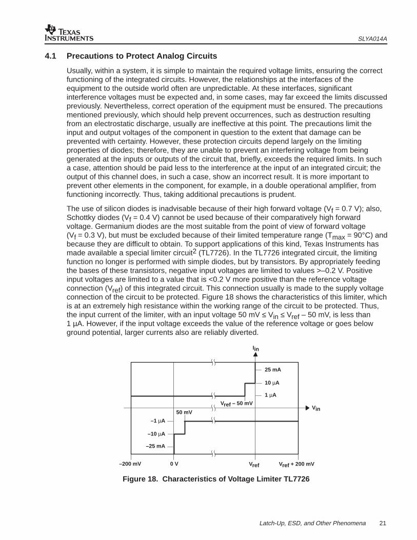
The use of silicon diodes is inadvisable because of their high forward voltage (Vf = 0.7 V); also,Schottky diodes (Vf = 0.4 V) cannot be used because of their comparatively high forwardvoltage. Germanium diodes are the most suitable from the point of view of forward voltage(Vf = 0.3 V), but must be excluded because of their limited temperature range (Tmax = 90°C) andbecause they are difficult to obtain. To support applications of this kind, Texas Instruments hasmade available a special limiter circuit2 (TL7726). In the TL7726 integrated circuit, the limitingfunction no longer is performed with simple diodes, but by transistors. By appropriately feedingthe bases of these transistors, negative input voltages are limited to values >–0.2 V. Positiveinput voltages are limited to a value that is <0.2 V more positive than the reference voltageconnection (Vref) of this integrated circuit. This connection usually is made to the supply voltageconnection of the circuit to be protected. Figure 18 shows the characteristics of this limiter, whichis at an extremely high resistance within the working range of the circuit to be protected. Thus,the input current of the limiter, with an input voltage 50 mV ≤ Vin ≤ Vref – 50 mV, is less than1 µA. However, if the input voltage exceeds the value of the reference voltage or goes belowground potential, larger currents also are reliably diverted.
Vin
–1 µA
–10 µA
–25 mA
50 mV
–200 mV 0 V Vref + 200 mVVref
1 µA
10 µA
25 mA
Iin
Vref – 50 mV
Figure 18. Characteristics of Voltage Limiter TL7726

SLYA014A
22 Latch-Up, ESD, and Other Phenomena
The operation of this voltage limiter can be explained simply. The voltage limiter is connected inparallel with the inputs of the component to be protected (see Figure 19). In addition, a resistor(Rs) must be inserted in each input line to limit the input current to an acceptable value. There isusually no difficulty choosing a suitable resistor; the high input resistance of modern operationalamplifiers and analog-to-digital (A/D) converters simplifies the choice of an appropriatecomponent. However, the limiter circuit has a comparatively high input capacitance which,together with the series input resistance Rs, influences the upper frequency limit of the completecircuit. In addition, digital-to-analog (D/A) converters, which contain a capacitor network in theconversion part of their circuitry, contribute an additional comparatively high input capacitance.This increases still further the low-pass characteristics of the protection circuit. The TL7726limiter tolerates high peak currents of short duration, making possible the use of low-ohmic-valueinput resistors.
VCC
MPX ADC/#
[Vref ] Z1
TL7726
1
Rs
AnalogInputs
+5 V
Figure 19. A/D Converter With Limitation of the Input Voltage

SLYA014A
23 Latch-Up, ESD, and Other Phenomena
4.2 High-Frequency Effects
Analog circuits usually have limited bandwidth. Thus, the transit frequencies (fT) of operationalamplifiers are only a few megahertz. From this point of view, a disturbance to the operation ofthese components as a result of high-frequency signals should be unlikely. In practice, casescan arise of a disturbance to the circuit as a result of interfering signals, the frequency of whichmight be several hundred MHz. On closer examination, the component has not been disturbeddirectly by the high-frequency radiation. Instead, the high-frequency interfering signal that isreceived by the connection lines that operate as an antenna is rectified by the nonlinear P-Njunctions in the semiconductor. These junctions include, for example, the diodes in theprotection circuits of the integrated circuits that are affected (see Figure 20). The nonlinear inputcharacteristic of an amplifier can cause it to function as a rectifier for high-frequency voltages orcurrents as a result of the audion effect. The dc voltage generated at this point can shift theworking point of a circuit significantly, putting the correct operation of the circuit into question.
Interconnecting Line = Antenna
Clamping Diode = RF Rectifier
InputTransistor
GND
Figure 20. Rectification of High-Frequency Interference Signals
Precautions to counter the effects described here include all possible methods forhigh-frequency decoupling of critical parts of the circuit. These precautions comprise adequatescreening of the sensitive parts of the circuit. Insertion of low-pass filters in sensitive input linesto attenuate high-frequency signals also can be effective.
4.3 Behavior of Logic Circuits
Parasitic transistors also are found in logic circuits, but the danger of a possible malfunction ofthe component as a result of unintentional switching on of a parasitic transistor is significantlyless than with analog circuits. It is not that the parasitic transistors are less sensitive, rather, thehigh noise margin that is common to all digital circuits is advantageous. Whereas, with analogcircuits, even the smallest currents that circulate in the substrate of the circuit can cause seriouserrors in the output signal, with logic circuits, considerably higher currents are necessary toproduce an incorrect logic level. In addition, semiconductor manufacturers take additionalprecautions in the form of additional guard rings to exclude, as far as possible, the influence ofparasitic transistors on the inputs and on the outputs of these devices.
Reflections that occur at the ends of lines that have not been terminated correctly causeovershoots and undershoots at the inputs and outputs of logic circuits. Figure 21 shows thewaveforms at the beginning and end of an open-circuit line having a characteristic impedance ofZo = 50 Ω, which is controlled by an SN74LVT244 device3. Because the end of the line is notterminated correctly, large overshoots and undershoots occur at this point. In theory, theamplitude would be double the voltage at the beginning of the line. As Figure 21 shows,reflections produce such overshoots and undershoots at the beginning of the line.

SLYA014A
24 Latch-Up, ESD, and Other Phenomena
7 V
6 V
5 V
4 V
3 V
2 V
1 V
0 V
–1 V
–2 V
–3 V
–4 V
–5 V0 ns 25 ns 50 ns 75 ns 100 ns 125 ns 150 ns 175 ns 200 ns
Figure 21. Waveforms on an Open-Circuit Line
In practice, clamping diodes limit the overshoots and undershoots in the integrated circuits towhich they are connected. These diodes must be able to pass relatively high currents withoutcompromising the function of the component. The amplitude of current ID in the clamping diodecan be calculated using equation 6.
ID 2 VCC
Zo
RoZo VCC VfD
Zo RfD
Where:VCC = Supply voltageZo = Characteristic impedance of the lineRo = Internal resistance of the line driverVfD = Forward voltage of the clamping diode (≈0.7 V)RfD = Differential resistance of the clamping diode
Without introducing any serious error, it can be assumed that Ro << Zo, and RfD << Zo. Thissimplifies equation 6 to:
ID VCC VfD
Zo
With a supply voltage of VCC = 3.3 V and a characteristic impedance of Zo = 30 Ω, which arefound in typical bus systems, the result is:
ID 3.3 V 0.7 V
30 80 mA
(6)
(7)
(8)

SLYA014A
25 Latch-Up, ESD, and Other Phenomena
Integrated-circuit design engineers lay out the clamping diodes, and the guard rings thatsurround them, so that currents that flow in the clamping diodes (and thus, inevitably, also in thesubstrate of the circuit) can be calculated to have approximate values of the magnitude inequation 8 and cause no malfunction of the circuit. This assumes that a switch-on duration of thecurrent of only a maximum of 100 ns with a duty cycle <10% is permitted. This limitation doesnot affect the logic circuits, because the overshoots and undershoots exist for only a fraction ofthe period of the wanted signals. The limitation of the switch-on time also makes it possible tokeep the area needed for the necessary guard rings within acceptable limits. Because the transitfrequency of the parasitic transistors is only about 1 MHz, shorter pulses in the range ofnanoseconds are unable to switch on these parasitic transistors. During testing, without powerfulpulse generators, a direct-current test usually is performed. A current of ID = 3 mA is injectedinto the clamping diodes for a duration of td = 10 µs to 20 µs. Extensive investigations show that,with 3 mA/10 µs, this test correlates sufficiently accurately to the assumed operating conditionsof 80 mA/100 ns.
5 Summary
An adequate understanding of both the characteristics and the limitations of integrated circuits isnecessary to develop a system that operates reliably under the required conditions. Theinformation given in semiconductor device data sheets often is insufficient to answer allquestions. This application report discusses relevant problems not covered in the data sheets,such as the latch-up effect in CMOS circuits. That semiconductor manufacturers take extensiveprecautions to prevent these problems arising in integrated circuits is reason enough for thedesign engineer to become acquainted with them. Care was taken in preparing this applicationreport to differentiate between the latch-up effect and other phenomena, which arise forcompletely different reasons, but are called latch-up. The situation is different with the immunityof integrated circuits to electrostatic discharges. Many test methods have been developed torealistically test the robustness of devices. However, all of these tests can provide an answeronly under particular operating conditions. Therefore, users must use data from themanufacturer to reach conclusions about the suitability of components in a specific situation andto take additional precautions as necessary.
The existence of so-called parasitic transistors in semiconductor devices can cause operationalproblems of which users should be aware. The basic cause of these problems has beenexamined in detail, together with the possible manifestation of parasitic transistors in actualcircuits. The discussion on parasitic transistors concluded with several precautions in systemdesign that can be taken to solve the latch-up problem.

SLYA014A
26 Latch-Up, ESD, and Other Phenomena
References1. James E. Vilson and Juin J. Liou, Electrostatic Discharge in Semiconductor Devices: An
Overview, Proceedings of the IEEE, Vol. 86, No. 2. February 1998.
2. Texas Instruments, Using the TL7726 Hex Clamping Circuit Application Report, literaturenumber SLAA004. (see http://www.ti.com/sc/docs/psheets/app_msp.htm)
3. Texas Instruments, Input and Output Characteristics of Logic Circuits Application Report,literature number SDZAE05.
Additional information on this subject:
4. Texas Instruments, Digital Design Seminar Manual, literature number SDYDE01A.
5. Texas Instruments, Data Transmission Seminar Manual, literature number SLLDE01C.
6. Texas Instruments, Linear Design Seminar Manual, literature number SLYDE05.
7. Texas Instruments, Logic Application Reports and Product Selection CD-ROM, literaturenumber SDZE01A.
8. Texas Instruments Internet site: http://www.ti.com

IMPORTANT NOTICE
Texas Instruments and its subsidiaries (TI) reserve the right to make changes to their products or to discontinueany product or service without notice, and advise customers to obtain the latest version of relevant informationto verify, before placing orders, that information being relied on is current and complete. All products are soldsubject to the terms and conditions of sale supplied at the time of order acknowledgment, including thosepertaining to warranty, patent infringement, and limitation of liability.
TI warrants performance of its semiconductor products to the specifications applicable at the time of sale inaccordance with TI’s standard warranty. Testing and other quality control techniques are utilized to the extentTI deems necessary to support this warranty. Specific testing of all parameters of each device is not necessarilyperformed, except those mandated by government requirements.
Customers are responsible for their applications using TI components.
In order to minimize risks associated with the customer’s applications, adequate design and operatingsafeguards must be provided by the customer to minimize inherent or procedural hazards.
TI assumes no liability for applications assistance or customer product design. TI does not warrant or representthat any license, either express or implied, is granted under any patent right, copyright, mask work right, or otherintellectual property right of TI covering or relating to any combination, machine, or process in which suchsemiconductor products or services might be or are used. TI’s publication of information regarding any thirdparty’s products or services does not constitute TI’s approval, warranty or endorsement thereof.
Copyright 2000, Texas Instruments Incorporated