labs 7-9 growing and observing micro and nanostructures · growing and observing micro and...
TRANSCRIPT
Growing and Observing
Micro and Nanostructures
2.674 Labs 7, 8 & 9
Spring 2016
Pappalardo II Micro/Nano Instructors: Teaching Laboratory Prof. Jeehwan Kim
Prof. Sang-Gook Kim Dr. Benita Comeau Mr. Andrew Jones
0
1
Labs 7, 8 and 9 expose students to nanomaterials through building (growing), touching and observing (imaging) them. During the lab tasks, students are encouraged to think how nanomaterials such as carbon nanotubes can be used for real world applications. Lab 7 begins with a “build” part to grow carbon nanotubes (CNTs). Chemical-vapor deposition (CVD) will be used to grow CNT forest on catalyst-coated silicon substrates. It will be shown that the growth of carbon nanotubes will be controlled by a few process parameters. In the “touch” part, you will drop one droplet of water onto the CNT forest surface and observe how it dynamically behaves using a high-speed camera. You will also observe the super-hydrophobic surface property of CNT forest by measuring the contact angle. In the Lab 8, students will observe various micro/nano objects including CNTs you grow, mouse embryos, AFM (Atomic Force Microscope) probe tips, atomic-sharp STM (scanning tunneling microscopy) tips and many PDMS samples you molded in the Lab 2 (Fun with Molding) with a scanning electron microscope (SEM). Students will get basic skills to operate electron microscopes and probe-based microscopes and interpret the images obtained from them. In Lab 9, students will fabricate high precision 3D structures by the micro 3D printing process. The digital light processing system successively projects thin sliced cross sections of the final product on the liquid UV pre-polymer, which vertically moves down to form a 3D structure.

2
Lab #7: Growing and Touching Carbon Nanotubes
I. Introduction 1. Carbon-based nanomaterials
Carbon is one of the most interesting elements among all existing elements appearing in a periodic table as it has various crystalline forms and the material properties substantially varies depending on the crystal structure. The basic building block of carbon-based nanomaterials is graphene. Graphene is a single-atom-thick two-dimensional sheet of sp2-bonded carbon [1]. As there are three laterally shared bondings in carbon atoms, a remaining vertical bond forms π-conjugation which is the source of exceptional electrical, thermal, and mechanical properties. This exceptional properties can be maintained by keeping its two-dimensional form. Once the graphene is three-dimensionally stacked, graphite is formed. Graphite is the most stable form of carbon allotropes. Although graphite is a conductive material, the electrical conductivity is not as high as graphene due to the disturbance between each graphene sheet. A graphite powder is a well-known dry lubricant. If the graphene is balled up into a hollow sphere, it becomes fullerene as a zero-dimensional form. However, the application space for fullerene is not as wide as graphene or carbon nanotubes. Carbon nanotubes (CNTs) can be formed by rolling graphene into tubes. CNTs maintain the most of superior properties of graphene although placement and manipulation of CNTs in nanoscale still remains challenging. However, CNTs can be semiconducting as they have the electrical band gap, while the graphene is semi-metallic due to no existence of its band gap. In the lab 7, we focus on understanding and fabrication of CNTs. We will revisit graphene in Lab 11.
Figure 1: Cartoons of carbon allotropes
© sources unknown. All rights reserved. This content is excluded from our CreativeCommons license. For more information, see https://ocw.mit.edu/help/faq-fair-use.

3
2. Carbon Nanotubes (CNTs) CNTs, first discovered by Iijima in 1991, are molecular-scale tubes made of graphitic carbon [2]. These cylindrical carbon molecules have novel properties that make them potentially useful in many applications in nanotechnology, electronics, optics and other fields of materials science. They exhibit extraordinary strength and unique electrical properties, and are efficient conductors of heat.
This image has been removed due to copyright restrictions.Please see https://commons.wikimedia.org/wiki/File:Types_of_Carbon_Nanotubes.png.
Figure 2: Cartoon of single-walled carbon nanotubes by rolling a graphene sheet in different angles, which defines the chirlity of a CNT.
CNTs can be categorized as single-walled (SWNT) or multi-walled (MWNT) depending on the number of graphene layers rolled into a tube; metallic or semiconducting depending on the chirality of rolled graphene layers. A SWNT is rolled with a single graphene layer, resulting a diameter of about 0.3~10 nm, though most of the observed SWCNTs have diameters <2 nm [3]. The structure of a SWCNT can be conceptualized by wrapping a one-atom-thick sheet of graphite (called graphene) into a seamless cylinder as shown in Figure 2. Depending on the angle that the graphene sheet is wrapped, different chirality of CNT results, which is represented by a pair of indices (a1, a2) called “the chiral vector, Ch = na1 +ma2 ,” as shown in Fig. 1. The integers, a1 and a2, denote the number of unit vectors along the two directions in the honeycomb crystal lattice of graphene. If a1=a2, the nanotubes are called “armchair”. If a1=0, the nanotubes are called “zig-zag”. Otherwise, they are called “chiral”. The diameter of a SWNT can be then calculated from
3athe equation, dtube= cc n2 +nm+m2 , where acc is the interatomic distance between π
C-C, ~ 1.42 Å.
MWNT is composed of multiple layers of graphene sheet rolled to form a multi-walled tube shape. The interlayer distance in MWNT is close to the distance between graphene layers of graphite, which is approximately 3.4 Å. Table 1 shows excellent properties of single-walled carbon nanotubes in comparison with several metals. It is noteworthy that the tensile strength of CNT is about 60 times higher that that of steel, and the specific strength is about 300 times higher that of steel. CNTs
This image has been removed due to copyright restrictions.Please see Figure 1.9 in http://www.ijera.com/papers/Vol3_issue4/LF3420252035.pdf.

4
also show exceptionally high mechanical resilience without breaking C-C bonds when they are subjected to compression, tension, bending and buckling loads.
Table 1. The properties of single-walled carbon nanotubes
Property SWNT Comparison
Size Diameter : 0.3 ~ 1.8 nm Human hair : ~50µm
Density 1.33~1.40 g/cm3 Al : 2.7 g/ cm3
Tensile Strength 40-60 G Pa Steel Alloy : 1-2 GPa
Young’s modulus 1.2 TPa Steel Alloy : 200 GPa
Current Carrying Capacity 1x10⁹ A/cm2 Copper Wires : 1x10⁶ A/cm2
Field Emission Phosphor : 1~3 V/㎛ Molybdenum tip : 50 ~ 100 V/㎛
Heat Transmission 6,000 W/m.k Diamond : 3,320 W/m.k
Several methods have been developed to synthesize (grow) carbon nanotubes. Generally, they can be classified by the CNT growing temperature; at high or at medium temperatures [4]. High-temperature routes are based on the electric arc or laser vaporization of a graphite target whereas medium-temperature routes are based on chemical vapor deposition (CVD) processes. High-temperature methods include Electric Arc Discharge and Laser Ablation methods, which, in general, cannot control the location and alignment of synthesized CNT. Medium-temperature routes include Plasma Enhanced Chemical Vapor Deposition (PECVD) and Thermal Chemical Vapor Deposition (T-CVD) methods. In this lab, we will use the Thermal CVD method to grow a CNT forest as shown in Figure 3.
Fig. 3 Vertically aligned carbon nanotubes with 10~20 nm diameter. (Grown by students, MIT 2.674)
3. Chemical Vapor Deposition (CVD)

5
Chemical Vapor Deposition (CVD) processes can grow carbon nanotubes and carbon filaments of various sizes and shapes at relatively low temperatures (≤ 1000 oC) from carbon-containing gaseous compounds which decompose catalytically on transition-metal particles. In CVD process, Fe, Co, Ni or a combination can be used as a metal catalyst layer. The catalytic metal nano particles can also be mixed with a catalyst support (such as MgO, Al2O3, etc) to increase the specific surface area for higher yield of the catalytic reaction of the carbon feedstock with the catalytic metal particles. The diameter of the nantobues depends on the size of the metal catalyst particles which is also related to the metal catalytic layer’s thickness. To initiate the growth of carbon nanotubes, two gases are inserted into the chamber: a reacting gas (such as ammonia, hydrogen, etc) and a hydrocarbon gas (such as acetylene, ethylene, methane, etc). It is generally accepted that CNTs can grow by the following three steps: (1) the decomposition of the hydrocarbon gases over a catalytic metal nanodot, (2) the diffusion of the carbon atoms through the bulk and surface of the catalyst, (3) the subsequent precipitation of the carbon atoms beneath the catalyst self-assemble into graphene layers. This is, however, still a hypothetical model and the CNT growing mechanism is still under investigation by many groups. The catalytic particles can remain at the tips of the grown CNTs during the growth process (top growth mode), or remain at the root of CNTs (bottom growth mode), depending on the adhesion between the catalyst and the substrate. In case of CNT growth by Plasma Enhanced Chemical Vapor Deposition, a strong electric field is generated during the growth of CNTs. Then, CNTs grow in the direction of the electric field and become vertically aligned whereas the CVD grown CNTs are randomly oriented without the plasma. In this lab, thermal chemical vapor deposition process will be used to grow carbon nanotubes into a forest on a silicon substrate.
4. Thermal Chemical Vapor Deposition System The CVD machine we will use consists of the following components: SabreTubeTM furnace (Absolute Nano: www.absolutenano.com) [5] and furnace heater controller, pre-heater and controller, gases and gas proportioner, and heating substrate.

6
Fig. 4: Thermal Chemical Vapor Deposition components
Fig. 5: SabreTube furnace

7
Fig. 6: Heater element
4.1. Tube furnace and controller The SabreTube furnace is a development tool (pre-commercial stage) that can be used for low pressure CVD processes, as well as other thermal and chemical processes such as material annealing and curing of thin films. The system is designed to operate at or below atmospheric pressures and has a safety relief valve that will be activated when the internal furnace pressure reaches at 0.3 psi (2.0 KPa) above atmospheric conditions. The heating element consists of highly doped silicon bar, which is 0.5 mm thick (see Fig. 6). The heating element is mounted within a quartz tube with lip seals on both ends. The tube allows full visual observation of the sample and process at all times. The temperature of the heating element is measured using an IR sensor mounted below the tube. This sensor has an equivalent output to a type K thermocouple (40 mV at 800oC). The heating element is designed to be removed/assembled without the use of any special tools, which enables quick sample loading/unloading. The furnace controller is a built-in control box including a power supply and an IR sensor output circuit.
• Heater power - This is the heating circuit. Applied voltage must be less than 50 V with a maximum current of 15 Amps.
• IR sensor output - This is a standard size panel mounted with a K type thermocouple jack on the rear of the furnace.

8
Fig. 7 Furnace controller
4.2 Pre-heater and controller The pre-heater heats incoming gases at 800oC before entering into the furnace tube. Although the gas cools partially when it exits the pipe and flows toward the substrate tube, thermal pre-treatment significantly affects the reactivity of the gas and can be utilized to substantially improve the rate and yield of CNT growth [6].
Fig. 8 Gas pre-heater and controller
Fig. 9 Gases and gas proportioner
9
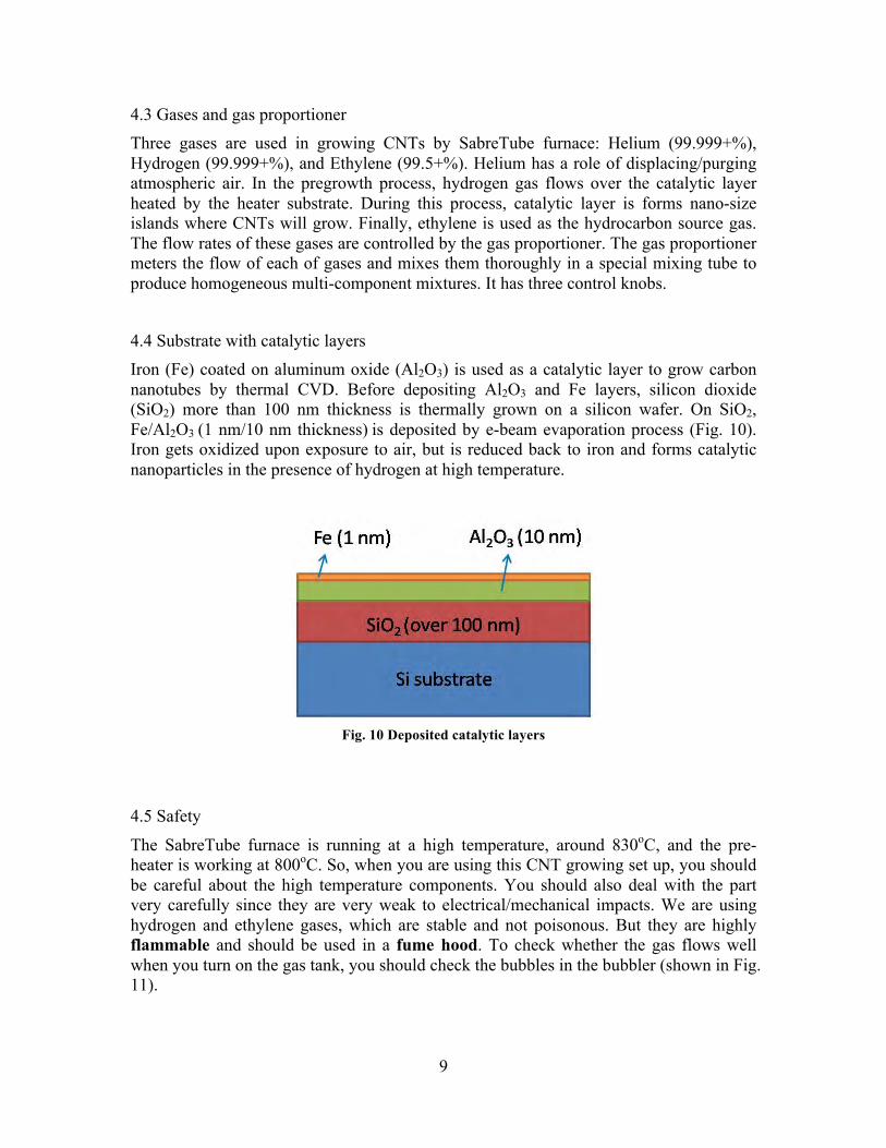
4.3 Gases and gas proportioner Three gases are used in growing CNTs by SabreTube furnace: Helium (99.999+%), Hydrogen (99.999+%), and Ethylene (99.5+%). Helium has a role of displacing/purging atmospheric air. In the pregrowth process, hydrogen gas flows over the catalytic layer heated by the heater substrate. During this process, catalytic layer is forms nano-size islands where CNTs will grow. Finally, ethylene is used as the hydrocarbon source gas. The flow rates of these gases are controlled by the gas proportioner. The gas proportioner meters the flow of each of gases and mixes them thoroughly in a special mixing tube to produce homogeneous multi-component mixtures. It has three control knobs.
4.4 Substrate with catalytic layers Iron (Fe) coated on aluminum oxide (Al2O3) is used as a catalytic layer to grow carbon nanotubes by thermal CVD. Before depositing Al2O3 and Fe layers, silicon dioxide (SiO2) more than 100 nm thickness is thermally grown on a silicon wafer. On SiO2, Fe/Al2O3 (1 nm/10 nm thickness) is deposited by e-beam evaporation process (Fig. 10). Iron gets oxidized upon exposure to air, but is reduced back to iron and forms catalytic nanoparticles in the presence of hydrogen at high temperature.
Fig. 10 Deposited catalytic layers
4.5 Safety
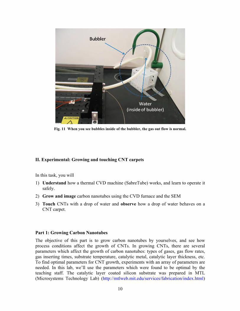
The SabreTube furnace is running at a high temperature, around 830oC, and the pre-heater is working at 800oC. So, when you are using this CNT growing set up, you should be careful about the high temperature components. You should also deal with the part very carefully since they are very weak to electrical/mechanical impacts. We are using hydrogen and ethylene gases, which are stable and not poisonous. But they are highly flammable and should be used in a fume hood. To check whether the gas flows well when you turn on the gas tank, you should check the bubbles in the bubbler (shown in Fig. 11).
10
Fig. 11 When you see bubbles inside of the bubbler, the gas out flow is normal.
II. Experimental: Growing and touching CNT carpets
In this task, you will 1) Understand how a thermal CVD machine (SabreTube) works, and learn to operate it
safely. 2) Grow and image carbon nanotubes using the CVD furnace and the SEM
3) Touch CNTs with a drop of water and observe how a drop of water behaves on a CNT carpet.
Part 1: Growing Carbon Nanotubes The objective of this part is to grow carbon nanotubes by yourselves, and see how process conditions affect the growth of CNTs. In growing CNTs, there are several parameters which affect the growth of carbon nanotubes: types of gases, gas flow rates, gas inserting times, substrate temperature, catalytic metal, catalytic layer thickness, etc. To find optimal parameters for CNT growth, experiments with an array of parameters are needed. In this lab, we’ll use the parameters which were found to be optimal by the teaching staff. The catalytic layer coated silicon substrate was prepared in MTL (Microsystems Technology Lab) (http://mtlweb.mit.edu/services/fabrication/index.html)

11
at MIT. The catalytic layers (Fe/Al2O3/SiO2) on a Si wafer were coated with 1/10/200 nm thickness, respectively. For safety, when you load and unload your sample, be careful not to touch a hot part in the furnace. Also, you should check that the gas valve is turned off.
Vph
H2
TphVplatformiplatform
C2H4
He
Gas tanks
Exhaust
Power supply Power supply
Preheater
Flowmeters w/manifold
V3
T3
Figure by MIT OpenCourseWare.
Fig. 12 Schematic diagram of the thermal CVD setup with gas tanks, gas proportioner, and power
supplies [5]
The procedure 1. Check all gases valves are closed firmly and the power of the furnace controller is off
before opening the slide door of the fume hood. 2. Open the slide door of fume hood, and remove the safety shield of the furnace.
3. To open the chamber, slide the quartz tube to the right direction carefully. When you touch the quartz tube, wear powder-free gloves (our gloves are powder-free).
4. Put two 8mm by 8 mm substrates on the heating substrate with the catalytic layer-coated side facing upward. Be careful not to push down on the heating substrate. Excess force on the heating substrate may break the heater. Cover the downstream side catalytic substrate with a silicon cap for observing the difference between results from covered and uncovered samples, Fig 12 (the non-polished side of the cap should contact the catalyst coated surface). Then, close the quartz tube and reinstall the safety shield. Slide down the window of the fume hood.

12
Fig. 13: Heated platform and growth substrate configuration
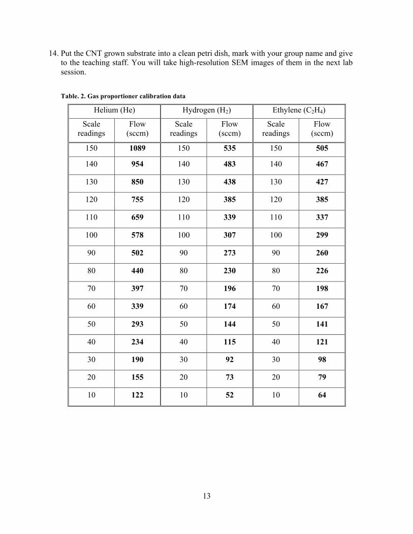
5. With the power to the heater and pre-heater controller remaining OFF, open the helium gas valve (the output indicators should read 50 psi) and adjust the helium gas knob of the proportioner to 1,000 sccm.1 (You can calibrate the scale readings of the proportioner using the flow meter calibration data sheet. See table 2). Leave it for 3 minutes.
6. While maintaining the Helium flow, plug in the power strip. The pre-heater will come on automatically and begin heating the pre-heater to 800oC. The heating substrate should remain unheated.
7. After the pre-heater reaches the set temperature (takes approximately 15~20 minutes), open the hydrogen gas valve and adjust the hydrogen gas knob to 250 sccm. Also, adjust the helium gas knob to 140 sccm (Remember that you should calibrate the scale readings with the data sheet), and wait for 2 minutes.
8. Maintaining these gas flow settings, turn the main power switch of the furnace controller ON. The set-point temperature will reach 830oC.
9. Turn on Heater Power Switch. When the temperature reaches 830 oC, leave it for 60 seconds to stabilize the temperature of the substrate.
10. While maintaining the same flow rates of helium and hydrogen gas, OPEN the ethylene gas valve and adjust the ethylene gas flow to 120 sccm (use the calibration sheet for the scale reading). The growth of carbon nanotubes starts.
11. After a desired growth time (in this lab, 30 minutes), shut off the hydrogen and ethylene gas valves together. Turn OFF the power switches of the furnace controller and pre-heater. Then, increase the helium gas flow rate to 1,000 sccm and leave it for 5 minutes.
12. Adjust the helium gas flow to 120 sccm for cooling the heating substrate. Wait until the chamber has cooled down to be touched (approximately 10~15 minutes).
13. Unload the sample by doing steps 1~3.
1 “sccm” stands for Standard Cubic Centimeters per Minute. Where "Standard" means referenced to 0 degrees Celsius and 760 Torr.
Figure by MIT OpenCourseWare.
13
14. Put the CNT grown substrate into a clean petri dish, mark with your group name and give to the teaching staff. You will take high-resolution SEM images of them in the next lab session.
Table. 2. Gas proportioner calibration data
Helium (He) Hydrogen (H2) Ethylene (C2H4)
Scale Flow Scale Flow Scale Flow readings (sccm) readings (sccm) readings (sccm)
150 1089 150 535 150 505
140 954 140 483 140 467
130 850 130 438 130 427
120 755 120 385 120 385
110 659 110 339 110 337
100 578 100 307 100 299
90 502 90 273 90 260
80 440 80 230 80 226
70 397 70 196 70 198
60 339 60 174 60 167
50 293 50 144 50 141
40 234 40 115 40 121
30 190 30 92 30 98
20 155 20 73 20 79
10 122 10 52 10 64

14
Lab data: Observe the CNT growth process and summarize it by filling the process table below.
Time [min] Gas Flow T preheater [oC] T substrate [oC] accumulated [sccm] setting setting
He H2 C2H4 Start: 0 min 1000 0 0 RT RT

Part 2: Super hydrophobic property of CNT forest The objective of this part is to observe the hydrophobic surface property of CNT forest. We will put one droplet of water on to the CNT forest surface and observe how it dynamically behaves using a high speed camera.
1. What is hydrophobicity?
In certain plant leaves such as lotus leaves, rain drops roll or bounce off these leaves, removing dirt, particles and dusts and keeping the surface clean. This phenomenon is known as “Lotus Effect,” which is the result of superhydrophobic surface of those leaves caused by nanostructured wax crystals on microstructured epidermal cells. (Figure 13)
This image has been removed due to copyright restrictions. This image has been removed due to copyright restrictions.Please see https://www.mpg.de/6855578/zoom.jpg. Please see http://www.dawntoduskpublications.
com/media/2009/Lotus_Leaf2.jpg.
Fig. 14 A water droplet on a lotus leaf. (W. Barthlott and C. Neinhuis, Planta 202, 1 (1997))
Spreading (wetting) of a liquid drop on a solid surface occurs when the specific work of wetting, Ws, is positive. When Ws is negative, the liquid droplet will not spread and form a contact angle as shown in Figure 14. The work of wetting, Ws, is zero at the solid-liquid-air triple boundary and the contact angle can be driven as γSG = γLG cosθ +γLS where γ refers to the interfacial tension and subscripts S, L and G refer to the solid, liquid and Gas (or air) phases respectively. This is the famous Young’s Equation. When this angle is less than 90o, the surface is hydrophilic; more than 90o, the surface is hydrophobic. If the angle is bigger than 150o, the surface is superhydrophobic. The lotus leaf is one of the natural superhydrophobic surfaces with a contact angle close to 1700. €
LG
θC
γ
SLγ
SGγ
Figure by MIT OpenCourseWare.
Fig. 15 Contact angle (θc) of a liquid droplet at the solid-liquid-air boundary is determined by the surface energies of them.
15

16
2. Nano-textured Superhydrophobic Surfaces Superhydrophobic surfaces can be made artificially by building micro- and nanostructured roughness on top of the already low surface energy solid surfaces as shown in Figure 16 [7, 8].
Kenneth K. S. Lau, Nano Letters, 3, 12, 2003
Figure 16: Superhydrophobic surfaces made by an array of silicon micropillars or CNT forest.
Earlier theoretical studies, including the works by Wenzel and by Cassie and Baxter, have revealed the role of surface texture on the interfacial properties. Further, with the recent development of micro/nano fabrication technologies, numerous research groups have exploited the understandings from these studies to develop applications such as self-cleaning surface coatings, anti-fogging films, and surfaces with drag-reduction property. If a small liquid droplet is placed on a textured surface, the contact leads to either a composite solid-liquid-air interface (Fig. 17 A) or a fully wetted Wenzel state (Fig. 17 B). In the former case, the liquid droplet attains its Young’s contact angle locally on the surface texture, a status, which is possible only when Young’s angle is equal to or greater than the geometric angle of the surface texture. Then the liquid does not fully penetrate into the pores of the surface texture. This results in a composite interface with the droplet sitting partially on air. This regime is also known as Cassie-Baxter status. If the surface texture cannot support the composite interface, the liquid penetrates into the texture and fully wets the surface. This state is also known as the Wenzel regime.
Fig. 17 A water droplet on textured surfaces
© sources unknown. All rights reserved. This content is excluded from our CreativeCommons license. For more information, see https://ocw.mit.edu/help/faq-fair-use.
This image has been removed due to copyright restrictions. This image has been removed due to copyright restrictions.Please see http://www.nature.com Please see Figure 1 on Page 17 of/nmat/journal/v1/n1/images/nmat715-f1.jpg.. http://web.mit.edu/nnf/publications/GHM72.pdf.

17
3. High speed camera CNT is known to be a low damping material and CNT forests can become superhydrophobic if treated with hydrophobic coating. What will happen when we drop a droplet of water at some height from the CNT forest surface? When a liquid drop impacts a solid, it spreads (with possibly beautiful fingering patterns) up to the point when kinetic energy is dissipated by viscosity. Then, it can retract on highly hydrophobic solids. On such solids, the kinetic energy of the impinging drop can be transferred to surface energy of the liquid, without spreading. Thus, the drop can fully bounce. The restitution coefficient, ε = |V’/V |, where V and V’ are, respectively, the velocities before and after the impact measured for each bounce. And the ratio of the kinetic energy over the liquid-air surface energy can be expressed via a dimensionless number, the Weber number. [9]
We = ρV 2R/γ
where γ the liquid surface tension and ρ its density. The droplet behavior changes drastically depending on the Weber number, by changing the droplet size and drop height. For the demonstration of bouncing water drops on a CNT forest surface, we will use a high speed camera which can take images with 1,000 fps as shown in Figure 18. The CNTs for this test are made more hydrophobic by exposure to a fluorocarbon silane.
Fig. 18 Water bouncing captured by high speed camera
Experiment procedure
1. Place one droplet (about 3-5 mm diameter on to a Si wafer, a CNT Forest surface and lotus leaf (front side) and take the digital camera images from the side. Measure the contact angles that the liquid makes at the solid-liquid-air triple boundary. Repeat the step by placing a smallest possible drop and the largest possible drop on them and compare their contact angles.
2. Take the high speed camera images when dropping one droplet of water on to a Si wafer, a lotus leaf and a CNT forest surface with a drop height about 1 cm. Repeat the drop test on the CNT forest by varying the drop height to 0.5 cm and 5 cm.
Height 1 Height 2 Height 3
CNT forest We
γ
Observation

18
Lotus leaf We
γ
Observation
Bare Silicon We One drop height
Observation:
for Si substrate is OK.
γ
Lab #7 Write-Up Questions: CNT growth 1. (1 point) Describe the role of the helium, hydrogen and ethylene gases in the CNT
growth process. 2. (1 point) What are the two major functions of the cap placed on the catalytic substrate
during the CNT growth?
3. (1 point) You will measure the length of your group’s CNTs in the Lab 8. Can you search for the longest CNT ever reported? Report this length along with a citation of the reference reporting the longest CNT that you found (e.g. journal paper, news article, webpage, etc.).
4. (2 points) If the SWCNT’s chirality is known to be (7, 7), what is the outer diameter of that CNT? Is this electrically conductive or not?
Drop Test on Super-hydrophobic Surface 5. (1 point) Measure and compare the contact angles (roughly) from the acquired images
of water droplets on silicon, CNT forest and lotus leaf. Also compare the contact angles of the smallest possible drop and the largest possible drop on CNT. Do you see any difference? Explain why or why not.
6. (4 points) By observing the water droplet’s bouncing behavior with 3 different drop heights, describe the drop behavior and estimate the Weber number and the restitution coefficient in each case (bare Si, lotus leaf, CNT forest). Use the table given in the experimental procedure to report your result. Show your work and equations used.
19
References [1] M. J. Allen, V. C. Tung, and R. B. Kaner, Chem. Rev. 110, 132–145 (2010)
[2] S. Iijima, “Helical micro-tubules of graphitic carbon”, Nature (London) 354 56 (1991) [3] R. Saito, G. Dresselhaus and M.S. Dresselhaus, Physical Properties of Carbon Nanotubes, Imperial College Press (1998) [4] A. Loiseau, P. Launois, P. Petit, S. Roche and J.-P. Salvetat, Understanding Carbon Nanotubes From Basic to Application, Springer (2006) [5] Absolute Nano, www.absolutenano.com
[6] A.J. Hart and A.H. Slocum, “Flow-mediated nucleation and rapid growth of millimeter scale aligned carbon nanotube structures from a thin-film catalyst”, Journal of Physical Chemistry B, 110 8250-8257 (2006) [7] A. Pozzato, et al., “Superhydrophobic surfaces fabricated by nanoimprint lithography,” Microelectronic Engineering, 83, 884-888, 2006 [8] K. K. S. Lau, et al., “Superhydrophobic Carbon Nanotube Forests,” Nano Letters, 3, 12, 1701-1705, 2003 [9] D. Richard and D. Quere,“Bouncing water drops,”775 (2000) [10] C. R. Oliver at al., “Statistical Analysis of Variation
Europhys. Lett., 50 (6), pp. 769–
in Laboratory Growth of Carbon Nanotube Forests and Recommendations for Improved Consistency”, ACSNano, V. 7, N. pp 3565 (2013)
20
Lab #8 Scanning Electron Microscope: Imaging Smaller than Light I. The Limits of Optical Microscopy An optical microscope uses a series of lenses to focus and bend light waves to create a magnified image of the specimen. The ability of a microscope lens to gather light is characterized by it’s numerical aperture, which is limited by the geometry of the lens and the refractive index of the medium through which the light passes. The classic optical microscope uses two magnification lenses, an objective lens and a condensing lens, with a range of numerical apertures. The Rayleigh criterion provides an estimate of the degree to which light diffracts as it passes through a small aperture, and can be used to estimate the resolution of an optical microscope for which the numerical aperture of the lenses is known.
1.22 ⋅ λResolution = (1) NAobj + NAcdn
where λ is wavelength of light, NAobj, numerical aperture of the objective lens, NAcdn is numerical aperture of the condensing lens. The relatively large wavelengths of light used in optical microscopy impose a practical limit on the maximum magnification of approximately 2000X. Or, the minimum possible resolution with the optical microscope can be estimated about 290 nm from the Equation (1) by putting NA=0.8, λ = shortest wavelength of visible light (380 nm). This is much bigger than most nanostructures, which implies that optical microscopy cannot image most nanostructures. What is the scientific base for the minimum resolvable details or resolution? How can we see micro and nano structures?
The resolution of any imaging process will be limited by diffraction. Diffraction refers to various phenomena that occur when a wave encounters an obstacle. It is described as the
bending of waves around small obstacles and the spreading out of waves past small openings or slits. Diffraction occurs with all waves, including sound waves, water waves, and electromagnetic waves such as visible light, x-rays and radio waves. Consider a case when a beam of light goes through a pinhole onto a dark background. If the image produced on the other side of the pinhole is examined,
one finds a light pattern known as an Airy disk which looks like a negative target with a large central disk of light surrounded by a series of thin concentric circles of light of decreasing brightness the further away from the center they are. An image of an Airy disk can be seen in Figure 2. The light beam coming out of the pinhole has been diffracted into several different orders represented by the concentric circles. The intensity of light can be measured as shown in Figure 3. The same thing
Figure 2 . Schematic of an optical microscope.
This image has been removeddue to copyright restrictions.Please see http://o.quizlet.com/iu5C08xIjOi6t-YFJitdKg_m.jpg.
© sources unknown. All rights reserved. This content is excluded from our Creative Commons license. For moreinformation, see https://ocw.mit.edu/help/faq-fair-use.
Figure 2. Intensity of a beam through a pinhole and Airy Disks around the pin hole

21
happens when light hits a microscopic specimen; the diffraction spreads out the light beam. The numerical aperture (NA) of an optical system is a dimensionless number that characterizes the range of angles over which the system can accept or emit light that can be seen as a cone with the half-angle θ that can enter or exit the lens. The bigger a cone of light that can be brought into the lens, the higher its numerical aperture is. Therefore the higher the numerical aperture of a lens, the better the resolution of a specimen will be which can be obtained with that lens. The numerical aperture of an optical system such as an objective lens is defined by
NA = nsinθ
where n is the index of refraction of the medium in which the lens is working (1.0 for air, 1.33 for pure water, and up to 1.56 for oils), and θ is the half-angle of the maximum cone of light that can enter the lens. The Rayleigh Criterion is the generally accepted a rough criterion for the minimum resolvable features with the following equation.
0.61⋅ λ λResolution = ≅ NA 2
Since the numerical aperture cannot be higher than ~1.6, we should find a way of using smaller wavelength lights in order to see or image sub-nanometer structure. An electron microscope is an instrument that produces a magnified image by a beam of electrons instead of light rays. An electron lens is an arrangement of electromagnetic coils that control and focus the electron beam. The wavelength of the electron beam is much shorter than that of light, so there may be much greater magnification; up to 2 million times. II. The Scanning Electron Microscope In his PhD thesis, published in Paris in 1924 Louis de Broglie put forward the idea that
any moving particle has an associated wavelength that is inversely proportional to the momentum of that particle. Using
This image has been removed de Broglie’s theory of wave-particle duality, it is possible to due to copyright restrictions. estimate the wavelength of an electron based on an estimate of Please see http://med.ardenne.de/ its momentum. Calculations based on his theory reveal that an wp-content/uploads/2012/07/MvA- electron would have a wavelength less than 0.01nm, depending am-UnivMikroskop.jpg.
on the momentum or energy of the electron. Electrons with higher energies have smaller wavelengths. While then Dr. de Broglie was receiving his Nobel Prize in 1929, a young researcher in Berlin named Ernst Ruska was working on the development of a cathode ray oscilloscope and investigating
Figure 3. Manfred von Ardenne at his electron microscope (1940). vacuum instrumentation and the physics of electron rays.
During his work, Ruska was able to experimentally prove the theory that a magnetic field, generated by a coil of wire through
which an electric current is passed, could be used to channel and focus a beam of electrons. It was this development of the electron lens that lead to the first electron

microscope in 1931, and then ultimately, in 1939, the scanning electron microscope developed by another German scientist, Manfred von Ardenne. Modern electron microscopes are very similar in design to those invented by Ruska and von Ardenne (you may notice that the SEM in Figure 3 looks a lot like the one in the teaching lab). In its most basic form, an SEM consists of five components: an electron source, commonly a tungsten filament heated up to 2800oC, a magnetic electron condensing lens, similar to those developed by Ruska, scanning coils used to generate magnetic fields that pull the beam of electrons back and forth across the sample, a detector used to detect the electrons scattered off the surface so an image can be formed, and finally, the entire system is kept under a vacuum with a series of pumps. In reality modern SEMs are often more complex. For example, most SEMs have multiple sets of condensing lenses to provide a more focused, higher resolution, beam as well as complex image processing equipment. Figure 4 shows a schematic of the electron beam column for the SEM in the teaching lab. You can notice our SEM has three condensing lenses. Imaging from an SEM can be as simple as
detecting emitted electrons, or it can involve measuring luminescence, emitted X-rays and current across the sample. Figure 5 is a schematic of the various surfaces emissions that can be used to image, or otherwise provide information about, a sample. When a beam of electrons hits the sample, the beam is either reflected or absorbed. Those electrons that are absorbed are either conducted through the sample, or reemitted as x-rays, secondary electrons or visible light (known as cathodoluminescence). The emitted, secondary electrons are most commonly used for topological imaging. They are attracted to a detector at a slight positive bias (~50V). The detector is designed
22
Figure 4. CamSacn Series 2 Scanning Electron Microscope Column Schematic. Image courtesy of Cambridge Scanning Co. Lt.
© Cambridge Scanning Co. Lt. All rights reserved.This content is excluded from our CreativeCommons license. For more information, seehttps://ocw.mit.edu/help/faq-fair-use.
This image has been removed due tocopyright restrictions.Please see http://img.tfd.com/ggse/60/gsed_0001_0030_0_img9334.png.
Figure 5. Electron beam / sample surface interactions used for imaging in a scanning electron microscope.

23
such that when an electron strikes it, it emits light in the visible range which is then amplified to create the image of the sample shown on the monitor. Even more information can be learned about the sample if the other emitted particles are detected and displayed. For example, detecting emitted X-rays can provide detailed information about material composition of the sample. Combining detection of all of the different surface emissions can yield very specific information about properties, thickness, and material of a sample as well as high resolution topological images.

24
III. Tescan SEM Vega3 Quick Operation Guide.
Only conductive samples can be explored in the high vacuum, so the specimen must be conductive or must be made conductive using one of the methods described in the technical reading matter. Further, the conductive surface of the specimen must have a conductive contact to the stub. The non-conductive samples can be investigated only in the low vacuum.
1. Plug the microscope into the mains voltage socket. Herewith the microscope is put into the Stand by state. In this state, the mains transformer in the vacuum electronics panel is connected, and the main switch is then functional.
2. Turn the main switch key to the right (ON position). Wait for the computer to boot.
3. Click on the VegaTC icon on the Windows desktop to start the microscope control program. The Log in screen is displayed prompting for user name and password. Type user name as “2674T9G1” and password “lab8”. Type your own group name accordingly. Passwords are same for the class.
4. After logging in, the latest microscope configuration will be loaded from the user profile. If a new user profile is created, load supervisor configuration. To open the dialog for loading saved configuration file, open the menu Options ,select Configuration item and click Load.
5. Start the pumping by clicking the button PUMP in the Vacuum Panel, which controls the vacuum system. The increase of the vacuum in this panel is indicated by the increase of the indication column. The working value attaining is indicated by the change of the column color to green.
6. Having reached the working vacuum, start the accelerating voltage by clicking the
button HV on the Electron Beam panel. If the specimen is inserted you should see the image, if not, check the value of the heating current, choose a suitable detector and set the optimal brightness and contrast of the image.

25
7. Select the accelerating voltage (0.5kV, 10kV and 30 kV) using combo box on the Electron Beam panel.
8. Click on Adjustment and click “Auto Gun Heating” after few second, click on
“Auto Gun Centering”. Also click on “Auto Column Centering.” This process will give you optimum beam setup for the chosen accelerating voltage.
9. Focus in the Resolution mode (click on the function Scan Mode in the Info Panel
and select RESOLUTION or use the function Continual Wide Field).
10. Clicking on the WD icon on the Floating Toolbar and turning the Trackball from left to right (or vice versa) focuses the image.
11. Select beam intensity, right-click on the BI icon on the Floating Toolbar and then select “Auto BI”.
12. Click on auto contrast/brightness.
13. Adjust magnification and scanning speed while keep adjusting focus
(WD) with icon and Trackball.
The TA or instructor will give you detail instruction for adjusting focus, saving image, exchanging samples during the lab session. Mouse embryos, gold coated lotus leaf, PDMS replica of lotus leaf, STM tips, CD and PDMS replica of CD, and AFM tips are already loaded. You will load CNT samples by yourself
Mouse embryos
AFM tip
STM tip
Lotus leaf and its PDMS replica
CD and its PDMS replica
26
Observing with the SEM We will observe the following objects using the SEM. Lab instructors will give the specimens at the lab session. You will be given a set of micro devices to image with the SEM: an AFM tip, STM tip, gold-coated bee, butterfly wings, and other samples. Imaging an AFM tip. An Atomic Force Microscope (AFM) consists of a microscale cantilever with a sharp tip (probe) at its end that is used to scan the specimen surface. The cantilever is typically silicon or silicon nitride with a tip radius of curvature in the order of 10s of nanometers. When the tip is brought into proximity of a sample surface, forces between the tip and the sample lead to a deflection of the cantilever, which is used to construct the image of the surface structures with sub nanometer resolution. Imaging Lotus leaf’s nanostructures In certain plant leaves such as lotus leaves, raindrops roll or bounce off these leaves, removing dirt, particles and dusts and keeping the surface clean. This phenomenon is known as “Lotus Effect,” which is the result of superhydrophobic surface of those leaves which have nanostructured wax crystals on microstructured epidermal cells. CNTs that you have grown Image the CNTs on silicon substrate. You can scratch the CNT forest with a razor blade to look at the cross-section of the CNT forest. Insect samples Observe the bee and butterfly wings. Image the eye lenses of the bee and scales of the butterfly. Lab #8 Write Up Questions All images must include scale bars.
© sources unknown. All rights reserved.This content is excluded from our CreativeCommons license. For more information,see https://ocw.mit.edu/help/faq-fair-use.
1. (1 point) Calculate the theoretical maximum resolution of the inverted microscope
(Nikon) in the teaching lab. Assume the microscope has a long working distance condenser lens (NA = 0.3) and a maximum 60x objective lens (NA = 1.0). Calculate the resolution for green light of wavelength 505 nm.
This image has been removeddue to copyright restrictions.Please see https://www.mpg.de/6855578/zoom.jpg.

27
2. (2 points) You are supposed to generate at least one SEM image by your own operation. Attach the image you took and describe the steps and tricks you used to get the best possible resolution and quality. For this question, you can choose any specimen. No one can claim the same image for this lab question; each student must produce their own image.
3. (2 points) Provide quantitative measurement of the AFM tip height (of the pyramid).
This can be done by tilting the object 30o or 45o away from you and use trigonometry to get the height. (90o tilting is not possible and do not try it.) Also make a quantitative measurement of the cantilever thickness in a similar manner. Present the images used for analysis and your calculations.
4. (1 point) Present image(s) of the nano patterns on lotus leaves. Include scale bar and describe features at different length scales that you observed.
5. (1 point) Observe the CNT your group grew and take best possible pictures. From the
SEM picture of CNTs, estimate the length of a typical CNT strand. You need to use some trigonometry to get the length from the tilted image. (Or you can scratch the CNT surface to make some of them loosely laid horizontally.)
6. (1 point) From the best zoomed-in image that you obtained, estimate the resolution of the microscope while acquiring that image. The resolution is the smallest distance between two point features at which they can be distinguished as two separate points.
7. (1 point) Present image(s) of a bee eye. Bees have compound eyes consisting of many
units called ‘ommatidia’. Measure and report the diameter of an ommatidium. 8. (1 point) Present image(s) of a butterfly wing. The wing consists of scales that give
the butterfly its colors due to interference of light.

28
Lab #9: Projection Micro-Stereolithography (PµSL)
I. Introduction
Projection micro-stereolithography (PµSL) is a type of additive three dimensional (3D) printing where an object is created using a UV-curable monomer resin with a projection or produced photo mask. PµSL is well suited to micro-scale devices and is a relatively simple way to produce small devices with micrometer scale resolution.
The process of PµSL (Figure 1) is to expose layers of UV polymerizing monomers to UV light projected by a laser reflecting on a digital micromirror device (DMD) or the white areas of a computer projector to cure. After curing, the stage is lowered so more monomer resin will flow over the cured layer and the next layer can be exposed. The monomer resin contains a UV absorbing dye to limit the depth of light penetration so lower layers are not cured. Finished printed objects are simply cleaned of the remaining monomer and can be used as devices, patterns, or molds.
The benefits of PµSL are that the equipment can be relatively low cost, the projection based mask is dynamic and easy to create, it can produce highly complex 3D parts, and it is simple system.
Stereolithography is one of several rapid prototyping methods that are being developed for desktop, 3D model making systems. The idea is to make a machine that is analogous to desktop printers, but for 3D objects. This method was first invented in 1984 by Charles Hull and new machines continue to be developed. One example of this is the Form 1 3D Printer from formlabs.com. This self-contained unit can produce objects with a minimum feature size of 300 µm, and a minimum layer thickness of 25 µm. Formlabs was spun-off from the MIT Media Lab in 2011, and Form 1 was funded on kickstarter.com. In fact, it is one of the most successfully funded ideas on kickstarter.com, reaching 2,945% of their goal funding! Even the New York Times has reported on 3D printing, with a 2010 article describing industry leading 3D systems from Stratasys, hobby kits from MakerBot Industries, and large scale 3D printing by Contour Crafting for building homes (http://www.nytimes.com/2010/09/14/technology/14print.html?pagewanted=all). More recently, the Times discussed the controversial application of using 3D printing to make custom firearms (http://www.nytimes.com/2013/01/30/science/surprising-tools-of-modern-gunmaking-plastic-and-a-3-d-printer.html?_r=0). Additionally, the PµSL system has many applications in MEMS, and current research interests are 3D microactuators, the possibility of creating grayscale masks for variable material properties, and 3D capillary arrays. All of these recent developments highlight the potential of stereolithography to augment the design process, and the impact of 3D printers was further recognized with the induction of Charles Hull into the National Inventors Hall of Fame in May 2014.
The process used in this lab is based on the work of Dr. Howon Lee and Professor Nicholas Fang in the Department of Mechanical Engineering at MIT, and previously at the University Illinois at Urbana-Champaign. The system is modeled after information provided by the Center for Nanoscale Chemical-Electric-Mechanical Manufacturing Systems (Nano-CEMMS) in collaboration with Dr. Fang's research group. The system is presented at http://nano_cemms.illinois.edu/materials/3d_printing_full.html . PµSL is an
29
exciting and easy way for the savvy Do It Yourself community to explore 3D printing on the millimeter scale. A tutorial for an automated system is available at http://3dlprint.com. Special thanks for Dr. Howon Lee for his help and patience on this project.
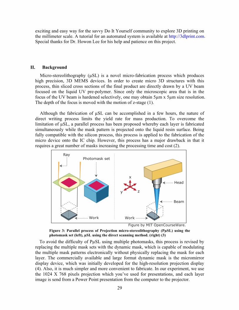
II. Background
Micro-stereolithography (µSL) is a novel micro-fabrication process which produces high precision, 3D MEMS devices. In order to create micro 3D structures with this process, thin sliced cross sections of the final product are directly drawn by a UV beam focused on the liquid UV pre-polymer. Since only the microscopic area that is in the focus of the UV beam is hardened selectively, one may obtain 5µm x 5µm size resolution. The depth of the focus is moved with the motion of z-stage (1). Although the fabrication of µSL can be accomplished in a few hours, the nature of direct writing process limits the yield rate for mass production. To overcome the limitation of µSL, a parallel process has been proposed whereby each layer is fabricated simultaneously while the mask pattern is projected onto the liquid resin surface. Being fully compatible with the silicon process, this process is applied to the fabrication of the micro device onto the IC chip. However, this process has a major drawback in that it requires a great number of masks increasing the processing time and cost (2).
Figure by MIT OpenCourseWare. Figure 3: Parallel process of Projection micro-stereolithography (PµSL) using the photomask set (left), µSL using the direct scanning method. (right) (3)
To avoid the difficulty of PµSL using multiple photomasks, this process is revised by replacing the multiple mask sets with the dynamic mask, which is capable of modulating the multiple mask patterns electronically without physically replacing the mask for each layer. The commercially available and large format dynamic mask is the micromirror display device, which was initially developed for the high-resolution projection display (4). Also, it is much simpler and more convenient to fabricate. In our experiment, we use the 1024 X 768 pixels projection which you’ve used for presentations, and each layer image is send from a Power Point presentation from the computer to the projector.
RayPhotomask set
Work Work
Beam
Headx
y z

30
Figure 4: Schematic of PµSL process: the white image from projector is focused by a condensing lens onto the stage which polymerizes the liquid polymer into a solid. After each exposure, the stage is lowered and exposed again, resulting in a 3D object.
The process of making 3D objects in our experiment is illustrated in Figure 2. The white image from computer to projection is focused on the stage for the exposure time, which is 8 seconds. The liquid goes through the polymerization process, transforming from uncured liquid monomer resin into cured solid polymer. After this process, the white image is removed and the stage is lowered down one step (a quarter turn), about 0.16mm. After the stage has lowered and the resin has had a few seconds to flow over the previous layer, the next white image is projected to cure the next layer. This process is repeated until the complete 3D object had been printed. In this lab, the monomer is a water-soluble PEG diacrylate (molecular weight 258, from Sigma-Aldrich, with viscosity 57 cP at 25°C). Bis(2, 4, 6-trimethylbenzoyl)-phenylphosphineoxide (97% powder from Sigma Aldrich) is used as the photo initiator. A small amount (0.05 wt%) of the UV adsorber Sudan I from Sigma Aldrich, is mixed
Figure by MIT OpenCourseWare.
8 Seconds
Projection image (mask)
Resulting object
Z
Projector
Condensing lens
Mirror
Cured polymer
Stage
Uncured polymer

31
with the PEG monomer to control the UV penetration depth in the solution. The liquid monomer cures into a solid polymer though the polymerization process. First, the photoinitiator generates radicals with exposure to UV light. The radicals, which each have a free electron, react with the monomer to begin the chain growth polymerization. Finally, the longer monomers that have a free electron interact with each other forming the polymer and terminating the process. Figure 3 shows a schematic view of the polymerization process and the steps created in the solid from each cure layer.
Figure 5: Schematic view of polymerization process (left) and the side view of the cured solid polymer showing the polymer growth direction is downward (right). The image was obtained by light microscope from a part made for the report testing.
Polymerization depth is proportional to the logarithm of UV light exposure time (5). It is also affected by the concentration of photoinitiator and photoabsorber. The photoabsorber absorbs the UV light and controls the penetration depth of UV light. If the photoabsorber is not added to this mixture, the UV light penetrates too deeply and forms a thick polymerized solid, which is not suitable for making thin layers of a 3D object. In this experiment, we use a fixed concentration of photoinitiator, photoabsorber, and UV light intensity, and only adjust the UV light exposure time. The polymerization process starts from the surface of the liquid and propagates downward. When the exposure time is not long enough, the curing depth is shallow and does not connect to the layer below, causing the separate layers to float and not form a continuous object. Therefore, curing time and the moving distance are important factors for obtaining a 3D object. Since the polymerization process is activated by UV light, projection of red produces very little UV light and can be used to project an image on the monomer without inducing polymerization. This is useful for focusing the image, and providing notes to the user. Each pixel of the Power Point image is projected to 45µm length in the system in our lab. It means that the 10x10 pixel of square image becomes 450µm x 450µm square on the stage. Also, lengths below 45µm are not obtainable on this system. If a magnifying lens that reduces the image 10 times on the stage were added, then this system could fabricate a 10 times smaller object. However, the total size of the object becomes 10 times smaller as well. There is a trade-off between the resolution and the total size of object in this system.
© sources unknown. All rights reserved. This content is excluded from our CreativeCommons license. For more information, see https://ocw.mit.edu/help/faq-fair-use.

III. Applications of PµSL
The PµSL system has many applications and current research interests include 3D microactuators, grayscale masks for variable material properties, tissue engineering, and 3D capillary arrays.
1. Microactuators based on Hydrogel Swelling Soft microactuators are achievable with several simple PµSL based designs. They function by absorbing
© sources unknown. All rights reserved. This content is
water into capillaries on one side of a
excluded from our Creative Commons license. For more
structure which causes swelling. The
information, see https://ocw.mit.edu/help/faq-fair-use.
swelling strains the structure and bends it, similar to the motion achieved by piezoelectric devices. These devices can be actuated by exposure to various stimuli including solvents, temperature, and light. The motion is reversible and can be
Figure 6:Time-lapsed leaf folding motion of artificial achieved in as little as 2 seconds, making micro Mimosa. Front view and top view. Scale bar these structures very useful for many indicates 500µm (6). soft robotics applications (6).
2. Grayscale Photo Masks The standard photomask system only utilizes the maximum (white) and minimum (black / red) intensity lighting to polymerize the monomer resin. An intermediate intensity light is also possible by utilizing a grayscale image. The grey will produce a continuously variable UV intensity which will yield a range
© sources unknown. All rights reserved. This content is
of material properties and can also be used
excluded from our Creative Commons license. For more
create support structures.
information, see https://ocw.mit.edu/help/faq-fair-use.
Support structures are commonly used in additive manufacturing to allow geometries to be built which are not self supporting and would collapse or warp without assistance. In PµSL, the issue is that each layer must be firmly connected to the previous layer or it will float out of place during later cure steps.
32 Figure 7: Full 3D object possible with grayscale scaffolding. A. Before acid etching, B and C after
acid etching, and D image of the etched tree without scaffolding (2).

33
A removable support structure is not reasonable due to the difficulty of mechanically removing micro scale components. By using grayscale, the supports can be partially cured and then etched away after printing due to their lower molecular weight (7).
3. Tissue Growth on Capillary Arrays and Scaffolding Tissue growth is currently limited by cell nutrient and oxygen transport because the cells in the middle of volume must rely on diffusion to gain the molecules need for life. Cell arrays need to be grown thicker than a few cells to produce medically useful tissue for grafting, but these cells require a capillary transport system similar to a living organism to maintain life. PµSL provides a possible solution to this issue by printing 3D arrays of capillaries. The polymers are semi-permeable, so thin tubes are able to mimic living capillaries. These arrays have been shown to promote growth in yeast cells and provide scaffolding for bone regrowth in frogs (8)
IV. Teaching Lab System
The system used in the teaching lab is modeled after a research PµSL machine in Professor Nicholas Fang's Lab with much lower cost equipment and lower resolution. The basic system components are schematically shown in Figure 2 and imaged in Figure 6. The system components are a computer to run Power Point or similar program, a projector, a condensing lens, a mirror, a linear stage with platform to lower the object as it grows, a beaker to hold the solution, and the monomer solution.
A commercial system costs about $200,000 due to its highly accurate equipment including a digital micromirror device to produce the laser imaging projection, a µm precision stage, and other precision equipment needed to achieve µm scale objects (4). The teaching system uses a standard computer projector instead of laser curing which results and a lower resolution, but significantly cheaper system. The current limit to feature size is about 400 nm (9) and the minimum feature size on the teaching lab system is 45 µm.

34
Figure 8: Image of teach system
Both systems can use the same chemicals to produce the models. The main component is the monomer resin, PEGDA 258 from Sigma Aldrich. Two percent by weight of Bis(2, 4, 6-trimethylbenzoyl)-phenylphosphineoxide from Sigma Aldrich is added as a photoinitiator to allow UV light to polymerize the monomer. Finally, 0.05% by weight of Sudan I from Sigma Aldrich, a photoabsorber, is added to prevent the UV light from curing all the way through the monomer when exposed. The chemical components are pictured in Figure 7. Changing the amount of photoabsorber would change the curing depth to cure time ratio. All the components need to be thoroughly mixed by a magnetic mixer to ensure uniformity prior to printing (9). Once the mixture is finished, it should have a shelf life of a few years as long as it is stored in a UV impenetrable container. The mixture is not toxic, although safety equipment should be used in accordance with standard lab safety.
Monomer Solution Projector
(ViewSonic PJD6221)
Linear Stage
Condensing Lens
Building Platform
Mirror

35
© sources unknown. All rights reserved. This content is excluded from our CreativeCommons license. For more information, see https://ocw.mit.edu/help/faq-fair-use.
Figure 9: Monomer liquid solution with PEGDA on magnetic stirrer (left), unmixed components (9) (right) Our system consists of the projector, magnifying glass, reflecting mirror, and stage. Powerpoint images are vertically focused on the moving stage after reflecting 90 degree off the reflecting mirror, and solidifying the PEGDA solution. Each layer is fabricated and moves down on the moving stage.
V. Laboratory Objectives
The goal of this lab is to experiment and become familiar with the PµSL process by performing a calibration test. Each lab group should choose between measuring depth of cure to exposure time or pixel to printing size mapping. Then the groups will share data to complete the lab questions. You will also be given the tools to make another fun object of your choosing or design if time allows. A list of pre-made exposure masks is available at http://nano-cemms.illinois.edu/materials/3d_printing_full.html.
VI. Experimental
The experimental set-up is quite simple and takes approximately 20 minutes to prepare and 15 minutes to make a ~1cm tall part. Note that Step 1 has been prepared for you ahead of time.
Step 1. Make the PEGDA solution Pour the 100 g PEGDA solution in the brown plastic bottle. Add 2g of Bis(2, 4, 6-trimethylbenzoyl)-phenylphosphineoxide, photoinitiator, and 0.05g photoabsorber. The solution should be mixed thoroughly which requires magnetic stirring for 2-3 hours due to the high viscosity of the liquids. The solution will last several years after mixing as long as the container protects the mixture from UV light. This step has already been done for you by the lab TA and instructors.

36
Step 2. Set up the Apparatus First, adjust the stage with the horizontal level using a bull eye (see Fig. 10) to make the platform as level as possible. The staging device moves on a threaded rod. Be sure the threaded rod is moved to the top to allow full range of movement when printing. The stage has a locking mechanism. Unlock the stage to pull it up or down. Position the beaker for the solution so that the stage is approximately 2 cm from the bottom, which gives enough space for the object.
Figure 10: Stage with Bulls eye (left), stage in bowl (right)
Turn the projector on and center the image on the stage. Adjust the projector so that the image is focused on the stage making sure there’s space about 2 cm from the bottom. You may also need to adjust the stage up and down so the image is in good focus. If the image travels as the stage moves up and down, the tilt of the mirror will need to be adjusted. Once the image is in the best focus, do not move the stage again. This will be the focal plane for your build.
Step 3: Power Point Open the projection images for the printing. The projections for the calibration testing are in Appendix 1 and more objects are available at http://nano-cemms.illinois.edu/materials/3d_printing_full.html. Each print only shows one mask of each type to keep the files small. The files need to be multiplied according the number of exposures listed on the slide so the full object is created. All exposure times should be the same. The exposure time should be for 8 seconds, but the optimal exposure time may vary between 5-10 seconds. Your instructor will let you know the best time to use. Turn on the projector by pressing the turn on button once. Turn off computer pop-ups since even a few seconds of exposure to a fully bright screen will expose a layer of the polymer and ruin the printed object. The first slide of the PowerPoint should be a screen full of red lettering which can be used to help focus the projector.
Step 5: Add mixture and run Turn the projector to the focusing slide and cover the lens with an opaque plastic plate to prevent the light from the projector from reaching the beaker. The red light has very little UV light, but it is still a good idea to limit exposure as much as possible. Fill the beaker with the pre-polymer resin mixture such that it just covers the stage with a thin

37
layer. Remove the plastic plate from in front of the lens and fine tune the focus on the surface of the stage. Advance the slides to the first layer and expose two times without moving the stage. Then start exposing each layer and moving the stage between each exposure. Project each image for the recommended time, alternating with a couple seconds of black screen. When the screen is blank, make a quarter turn on the knob to lower the stage and allow fresh pre-polymer resin to flow over the top. Then go to the next slide and expose. Once the object is finished, cover the projector lens again and remove the object with tweezers. Be gentle since the object is fragile and start by scraping the bottom off of the stage with a sharp blade. Clean the object with isopropyl alcohol and water, and look at it under a microscope to answer the write up questions.
Lab #9 Write-Up Questions
1. (2 points) Using the image of a block, calculate the pixel to actual length ratio.
Show how you obtained this value. (Each block is 15 x 15 pixel)
2. (4 points) Using the working curve equation, ), verify that your
test structure data follow this equation and find the constant values for Dp and Ec. Recall from the lecture notes that Emax, the maximum exposure, is the exposure dose at the surface of the resin. Ec is the critical exposure threshold, below which polymerization into a solid will not occur. Cd is the cured depth of the piece, and Dp is the penetration depth of the resin.
a. Measure the light intensity b. Build the test structure with lines of varying exposure times c. Calculate the exposure dose for each exposure time d. Measure the thickness of each cured line to experimentally determine Cd e. Plot Cd vs. ln(Emax) and do a best fit line to extract the resin parameters Dp
and Ec
3. (2 points) Explain how you determined the optimal start height for the build platform and why finding this position is important for building your structure.
4. (1 point) When you start the process, we recommend that you repeat the first exposure a couple of times. Why does this help in the building of the structure?
5. (1 point) Were all of your structures built correctly and accurately? If there was deformation of the thin layers, what do you think was the cause?

38
Appendix 1: Images of Test Structures
Figure 12: Pixel calibration block (left), Exposure depth vs. curing depth structure (right)

39
Appendix 2: Projection Masks
Exposure Time - Depth (4)
XXXXXXXXXXXXXXXXXXXXXXXXXXXXXXXXXXXXXXXXXXXXXXXXXXXXXCreatedByNeilTewksburyXXXXXXXXXXXXXXXXXXXXXXXXXXXXXXXXXNextGenerationMiddleSchoolXXXXXXXXXXXXXXXXXXXXXXXXXXXXXXXXXXXXXXXXXXXXXXXXXXXXXXXXXXXXXXXXXXXXXXXXXXX
Repeat 5 times Quarter turn Exposure time 8s
Repeat 5 times Quarter turn Exposure time 8s
Exposure Time 1s to 13s Interval 3s
Figure 13: Exposure time to polymerization depth calibration

40
Calibration Block width=15pixels, gap=15pixels
XXXXXXXXXXXXXXXXXXXXXXXXXXXXXXXXXXXXXXXXXXXXXXXXXXXXXCreatedByNeilTewksburyXXXXXXXXXXXXXXXXXXXXXXXXXXXXXXXXXNextGenerationMiddleSchoolXXXXXXXXXXXXXXXXXXXXXXXXXXXXXXXXXXXXXXXXXXXXXXXXXXXXXXXXXXXXXXXXXXXXXXXXXXX
Figure 14: Projection pixel to print size calibration block. Each square in the bottom right panel is 15 x 15 pixels.

41
References 1. Koji Ikuta et al. "Real Three Dimensional Micro Fabrication Using Stereolithography and
Metal Moding" IEEE Micro Electro Mech, 1993. 2. Sun, C., N. Fang, D. M. Wu, and X. Zhang, “Projection Micro-Stereolithography Using
Digital Micro-Mirror Dynamic Mask,” Sensors and Actuators A, 121:1, 113-120, (2005). 3. Takagi, Tarou. "Photoforming Applied to Fine Machine" IEEE Micro Electro Mech, 1993.
p.1734. Yoshikazu Hirai et al. "Moving mask UV lithography for three-dimensional structure".
Journal of Micromechanics and Micro Engineering, 2007, Vol. 17. pg. 199-206 5. Lee, Howon, Xia, C. Fang, Nicholas "Biometric Microactuator Powered By Polymer
Swelling". ASME International Mechanical Engineering Congress and Exposition, 2008. IMECE2008-67594.
6. C.G. Xia and N. X. Fang, “Fully three-dimensional micro fabrication with grayscale polymeric self-sacrificial structure”, Journal of Micromechanics and Microengineering, Vol 19:11, art. no. 115029(2009).
7. C.G. Xia and N. X. Fang, “3D Microfabricated Bioreactor with capillaries”, Biomedical Microdevices. Vol. 11:6, 1309-1315,(2009).
8. Center for Nanoscale Chemical-Electric-Mechanical Manufacturing Systems. 3d Printing. Febuary 10, 2012. http://nano-cemms.illinois.edu/materials/3d_printing_full.html.
9. Stepper Motor - 29 oz.in. SparkFun Electronics. http://www.sparkfun.com/products/10848.
10. Yoshikazu Hirai et al, “Moving mask UV lithography for three dimensional structuring”, Journal of Micromechanics and Microengineering, 2007, vol. 17, p. 199-206
11. Xia, C. Three-Dimensional Polymeric Capillary Network: Fabrication and Applications, in Mechanical Science and Engineering. 2009, University of Illinois at Urbana -Champaign: Urbana, Illinois. p 117.
12. C.G. Xia, Howon Lee, and N. X. Fang, "Solvent Driven Polymeric Bistable Device" Journal of Microelectromechanical Systems, pp. 1309 – 1315.

MIT OpenCourseWarehttps://ocw.mit.edu
2.674 / 2.675 Micro/Nano Engineering LaboratorySpring 2016
For information about citing these materials or our Terms of Use, visit: https://ocw.mit.edu/terms.