two-dimensional nanostructures: thin films - portalweb.eng.fiu.edu/wangc/two-dimensional...
TRANSCRIPT

1
Two-Dimensional Nanostructures: Thin Films
Dr. Chunlei (Peggy) WangMechanical and Materials Engineering
Florida International University
Nanowires and Nanorods

2
Content� Physical vapor deposition
(PVD)
� Thermal evaporation
� Sputtering
� Evaporation and sputtering compared
� MBE
� Laser sputtering
� Ion Plating
� Cluster-Beam
� Chemical vapor deposition (CVD)
� Reaction mechanisms
� Step coverage
� CVD overview
� Epitaxy
� Electrochemical Deposition
Physical vapor deposition (PVD)
� The physical vapor deposition technique is based on the formation of vapor of the material to be deposited as a thin film. The material in solid form is either heated until evaporation (thermal evaporation) or sputtered by ions (sputtering). In the last case, ions are generated by a plasma discharge usually within an inert gas (argon). It is also possible to bombard the sample with an ion
beam from an external ion source. This allows to vary the energy and intensity of ions reaching the target surface.

3
Physical vapor deposition (PVD)
Physical vapor deposition (PVD): thermal evaporation
Heat Sources Advantages Disadvantages
Resistance No radiation Contamination
e-beam Low contamination Radiation
RF No radiation Contamination
Laser No radiation, lowcontamination
Expensive
N = N o exp- Φ e
kT
6
The number of molecules
leaving a unit area of evaporant
per second

4
Physical vapor deposition (PVD): thermal evaporation
Physical vapor deposition (PVD): thermal evaporation
Si
Resist
d
ββββ
θθθθEvaporant container with orifice diameter DD
Arbitrary surface element
1-exp (+d/λλλλ)
Kn = λλλλ/D > 1
A ~ cosββββ cos θθθθ/d2
N (molecules/unit area/unit time) =3.513.1022Pv(T)/ (MT)1/2
The cosine law
This is the relation between vapor pressure of
the evaporant and the evaporation rate. If a high
vacuum is established, most molecules/atoms will reach
the substrate without intervening collisions. Atoms and
molecules flow through the orifice in a single straight
track,or we have free molecular flow :
The fraction of particles scattered by collisions
with atoms of residual gas is proportional to:
The source-to-wafer distance must be smaller than the mean free path (e.g, 25 to 70 cm)
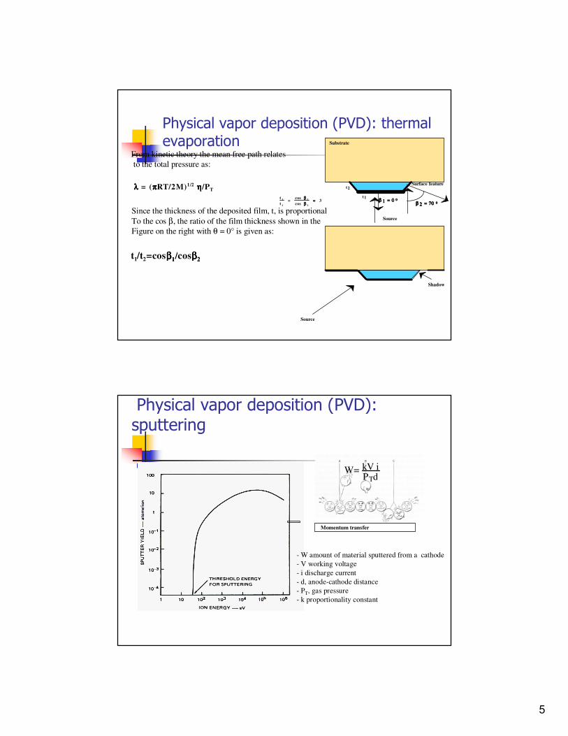
5
Physical vapor deposition (PVD): thermal evaporation
ββββ 2222 = 70 = 70 = 70 = 70 0000ββββ 1111 = 0 = 0 = 0 = 0 0000
t2
t1
Substrate
t 1
t2
= cos ββββ 1
cos ββββ 2
≈≈≈≈ 3
Surface feature
Source
Source
Shadow
t1/t2=cosββββ1111/cosββββ2222
λλλλ = (ππππRT/2M)1/2 ηηηη/PT
From kinetic theory the mean free path relates
to the total pressure as:
Since the thickness of the deposited film, t, is proportional
To the cos β, the ratio of the film thickness shown in the
Figure on the right with θ = 0° is given as:
Physical vapor deposition (PVD): sputtering
W= kV iPTd
- W amount of material sputtered from a cathode
- V working voltage
- i discharge current
- d, anode-cathode distance
- PT, gas pressure
- k proportionality constant
Momentum transfer

6
Evaporation
and sputtering:comparison
Evaporation Sputtering
Rate Thousand atomic layers per second
(e.g. 0.5 µm/min for Al)
One atomic layer per second
Choice of materials Limited Almost unlimited
Purity Better (no gas inclusions, very high
vacuum)
Possibility of incorporating
impurities (low-medium vacuum
range)
Substrate heating Very low Unless magnetron is used substrate
heating can be substantial
Surface damage Very low, with e-beam x-ray
damage is possible
Ionic bombardment damage
In-situ cleaning Not an option Easily done with a sputter etch
Alloy compositions,stochiometry
Little or no control Alloy composition can be tightly
controlled
X-ray damage Only with e-beam evaporation Radiation and particle damage is
possible
Changes in sourcematerial
Easy Expensive
Decomposition ofmaterial
High Low
Scaling-up Difficult Good
Uniformity Difficult Easy over large areas
Capital Equipment Low cost More expensive
Number ofdepositions
Only one deposition per charge Many depositions can be carried
out per target
Thickness control Not easy to control Several controls possible
Adhesion Often poor Excellent
Shadowing effect Large Small
Film properties (e. g.grain size and stepcoverage)
Difficult to control Control by bias, pressure,
substrate heat
Physical vapor deposition (PVD): MBE, Laser Ablation
-
� MBE
� Epitaxy: homo-epitaxyhetero-epitaxy
� Very slow: 1µm/hr
� Very low pressure: 10-11
Torr
� Laser sputter deposition
� Complex compounds (e.g. HTSC, biocompatible ceramics)

7
Physical vapor deposition (PVD): Ion cluster plating
� Ionized cluster: it is possible to ionize atom clusters that are being evaporated leading to a higher energy and a film with better properties (adherence, density, etc.).
� From 100 mbar (heater cell) to 10-5 to 10-7 mbar (vacuum)--sudden cooling
� Deposits nanoparticles
� Combines evaporation with a plasma
� faster than sputtering
� complex compositions
� good adhesion
� Gas cluster ions consist of many atoms or molecules weakly bound to each other and sharing a common electrical charge. As in the case of monomer ions, beams of cluster ions can propagate under vacuum and the energies of the ions can be controlled using acceleration voltages. A cluster ion has much larger mass and momentum with lower energy per atom than a monomer ion carrying the same total energy. Upon impact on solid surfaces, cluster ions depart all their energy to an extremely shallow region of the surface. Sputtered material is forced sideways and produces highly lateral sputtering yields. These sputtering properties are unique to gas cluster ions and produce smoother surfaces.
� Also individual atoms can be ionized and lead to ion plating (see figure on the right, example coating : very hard TiN)
Physical vapor deposition (PVD):Ion cluster plating and ion plating

8
Chemical vapor deposition (CVD): reaction
mechanisms
� Mass transport of the reactant in the bulk
� Gas-phase reactions (homogeneous)
� Mass transport to the surface
� Adsorption on the surface
� Surface reactions (heterogeneous)
� Surface migration
� Incorporation of film constituents, island formation
� Desorption of by-products
� Mass transport of by-products in bulk
CVD: Diffusive-convective transport of depositing species to a substrate with many intermolecular collisions-driven by a concentration gradient
SiH4SiH4
Si
Chemical vapor deposition (CVD): reaction mechanisms
Fl = D∆c
∆x
δ(x) =ηx
ρU
1
2
δ =1
Lδ(x )dX =
2
30
L
∫ Lη
ρUL
1
2
ReL =ρUL
ηδ = 2L
3 ReL
� Energy sources for deposition:
� Thermal
� Plasma
� Laser
� Photons
� Deposition rate or film growth rate (Fick’s first law)
(gas viscosity η, gas density ρ, gas stream velocity U)
(Dimensionless Reynolds number)
Laminar flow
L
δ(x)
dx
(U)
(Boundary layer thickness)
Fl = D∆c
2L3 ReL (by substitution in Fick’s first law and ∆x=δ)

9
� Mass flow controlled regime (square root of gas velocity)(e.g. AP CVD~ 100-10 kPa) : FASTER
� Thermally activated regime: rate limiting step is surface reaction (e.g. LP CVD ~ 100 Pa----D is very large) : SLOWER
Chemical vapor deposition (CVD)
: reaction mechanisms
Fl = D∆c
2L3 ReL
R = Ro e -
Ea
kT
LPCVD for Si Technology

10
Chemical vapor deposition (CVD): step coverage
Fl = D∆c
2L3 ReL
R = Ro e -
Ea
kT
� Step coverage, two factors are important
� Mean free path and surface migration i.e. P and T
� Mean free path: λ =
αααα
w
zθ=180θ=180θ=180θ=1800000
θ=270θ=270θ=270θ=2700000θ=90θ=90θ=90θ=900000
θ is angle of arrival
kT
2
1
2 PTπa2
> α
Fldθ∫
θ = arctanw
z
Chemical vapor deposition (CVD) : overview
� CVD (thermal)
� APCVD (atmospheric)
� LPCVD (<10 Pa)
� VLPCVD (<1.3 Pa)
� PE CVD (plasma enhanced)
� Photon-assisted CVD
� Laser-assisted CVD
� MOCVD
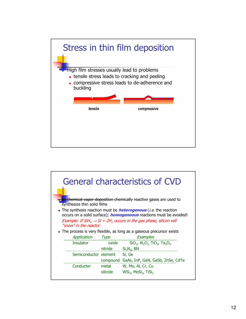
Tensile stress causes concave bending of a thin substrate
Compressive stress causes convex bending of a thin substate
Deposited film
Deposited film
P148 Table 3.10 Review of CVD processes

11
Stress in thin film deposition
� Most films, when deposited, are stressed with respect to the substrate
� Thermal mismatch stress
� arises when the deposition is performed at a temperature different from room temperature
� difference in thermal expansion coefficients of the film and the substrate will lead to stress
� obviously as the deposition temperature increases, the magnitude of the stress increases
( )dTE T
To∫ α−α
ν−=σ
dep
subfilm
film
filmth
1
� Intrinsic stress is the stress that arises during deposition process due to the nature of the process itself
� There are at least three common sources of intrinsic stress:� chemical reactions during the deposition process
� Ti deposition in poor vacuums can develop compressive stress due to continued oxidation beneath the surface
� microstructure and defects� densification of (microscopic) vacancies and (macroscopic) voids will generate tensile stresses; these can be very large
� particle bombardment� implantation of ions or energetic neutrals lead to compressive stress in the layer due to interstitials
� The magnitude of the net intrinsic stress will be very sensitive to the details of the deposition process
Chemical vapor deposition (CVD) : overview
12
Stress in thin film deposition
� High film stresses usually lead to problems
� tensile stress leads to cracking and peeling
� compressive stress leads to de-adherence and buckling
tensile compressive
General characteristics of CVD
� In chemical vapor deposition chemically reactive gases are used to synthesize thin solid films
� The synthesis reaction must be heterogenous (i.e. the reaction occurs on a solid surface); homogeneous reactions must be avoided!
Example: If SiH4 → Si + 2H2 occurs in the gas phase, silicon will “snow” in the reactor
� The process is very flexible, as long as a gaseous precursor exists
Application Type Examples
Insulator oxide SiO2, Al2O3, TiO2, Ta2O3
nitride Si3N4, BN
Semiconductor element Si, Ge
compound GaAs, InP, GaN, GaSb, ZnSe, CdTe
Conductor metal W, Mo, Al, Cr, Cu
silicide WSi2, MoSi2, TiSi2

13
⇒ introduce chemically reactive species into a reactor
⇒ diffusion of the reactants to the surface
⇒ adsorption of the reactants onto the surface
⇒ reaction at the surface to form the solid
⇒ desorption of the reaction products from the surface
⇒ diffusion of the reaction products away from the surface
⇒ transport of the reaction products out of the reactor
General characteristics of CVD
� All CVD reactions follow the same generic elementary
processes seen earlier in etching reactions:
� The final deposition rate will be determined by the slowest
one of these processes (the “rate limiting step”)
Generic CVD reactions (an abbreviated list)
� pyrolysis: SiH4(g) → Si(s) + 2H2(g)
� reduction: SiCl4(g) + 2H2(g) → Si(s) + 4HCl (g)
� oxidation: SiH4(g) + O2(g) → SiO2(s) + 2H2(g)
� nitride formation: 3SiH4(g) + 4NH3 → Si3N4(s) + 12H2(g)
� carbide formation: TiCl4(g) + CH4(g) → TiC(s) +
4HCl(g)
� organometallicreaction: (CH3)3Ga(g) + AsH3(g) → GaAs(s) + 3CH4(g)
� chemical transportreaction: 6GaAs(s) + 6HCl(g) ↔ As4(g) + As2(g) +
GaCl(g) + 3H2(g)
T1
T2
T1>T2 creates gas-phase species; lowering the temperature
downstream reverses the reaction and deposits GaAs

14
� The LCVD method is able to fabricate continuous thin rods and fibres by pulling the substrate away from the stationary laser focus at the linear growth speed of the material while keeping the laser focus on the rod tip, as shown in the Figure . LCVD was first demonstrated for carbon and silicon rods. However, fibres were able to grown from hundreds of substrates including silicon, carbon, boron, oxides, nitrides, carbides, borides, and metals such as aluminium. The LCVD process can operate at low and high chamber pressures. The growth rate is normally less than 100 µm/s at low chamber pressure (<<1 bar). At high chamber pressure (>1 bar), high growth rate (>1.1 mm/s) has been achieved for small-diameter (< 20 µm) amorphous boron fibres.
Chemical vapor deposition (CVD) : L-CVD
Epitaxy
� VPE:
� MBE (PVD) (see above)
� MOCVD (CVD) i.e.organo-metallic CVD(e.g. trimethylaluminum to deposit Al) (see above)
� Liquid phase epitaxy
� Solid epitaxy: recrystallization of amorphous material (e.g. poly-Si)
Liquid phase epitaxy

15
Epitaxy
� Selective epitaxy
� Epi-layer thickness:
� IR
� Capacitance,Voltage
� Profilometry
� Tapered groove
� Angle-lap and stain
� Weighing
Selective epitaxy
Electrochemical deposition: electroless
� Electroless metal displacement
� Electroless sustainable oxidation of a reductant
� Metal salt (e.g.NiCl2)
� Reductant (e.g.hypophosphite)
� Stabilizer:bath is thermodynamically unstable needs catalytic poison (e.g. thiourea)
� Complexing agent : prevent too much free metal
� Buffer: keep the pH range narrow
� Accelerators: increase deposition rate without causing bath instability (e.g. pyridine)
� Deposition on insulators (e.g. plastics): seed
surface with SnCl2/HCl
1. Zn(s) + Cu 2+(aq) ------> Zn 2+(aq) + Cu(s)
2. Reduction (cathode reaction) :
Ni+2 + 2e- —> Ni
Oxidation (anode reaction):
H2PO 2- + H2O—> H2PO3
- +2H+ +2e- ------------------------------------------
Ni+2 + H2PO2- + H2O —> Ni + H2PO3
- + 2H+
e.g. electroless Cu: 40 µmhr-1
Cu

16
Electrochemical deposition: electroless
� Evan’s diagram: electroless deposition is the combined result of two independent electrode reactions (anodic and cathodic partial reactions)
� Mixed potential (EM): reactions belong to different systems
� ideposition = ia = ic and I=A x i deposition� Total amount deposited: m max= I t
M/Fz (t is deposition time, Molecular weight, F is the Faraday constant, z is the charge on the ion)
� CMOS compatible: no leads required
Evan’s diagram
F= 96,500 coulombs=1, 6 10 -19 (electron charge) x 6. 02 10 23 (Avogadro’s number)
+
-
Electrochemical deposition :electrodeposition-thermodynamics
� Electrolytic cell
� Au cathode (inert surface for Ni deposition)
� Graphite anode (not attacked by Cl2)
� Two electrode cells (anode, cathode, working and reference or counter electrode) e.g. for potentiometricmeasurements (voltage measurements)
� Three electrode cells (working, reference and counter electrode) e.g. for amperometric measurements (current measurements)

17
Electrochemical deposition :electrodeposition-thermodynamics (E)
E = E0
+RT
zFln a
Mz +
² G=² G2-² G1 ² G = -(E 2-E1)zF = -EcellzF
² G=² G0-RT ln aMz+=² G0-RT ln CMz+γΜ z+
² G= - EzF
E2 > E1 : - battery
E2 < E1 : + E ext > E cell to afford deposition
(Nernst equation)
1. Free energy change for ion in the solution to atom in the metal (cathodic reaction):
or also
2. The electrical work, w, performed in electrodeposition
at constant pressure and constant temperature:
and since ∆V =0
∆ G = G m (free energy pure metal) - G e (free energy of ion in the electrolyte)
∆G = - w + P∆V
3. Substituting Equation (2) in (1) one gets
(1)
(2)
4. Repeat (1) and (2) for anodic reaction:
or
Electrochemical deposition :electrodeposition-thermodynamics (η)
� A thermodynamic possible reaction may not occur if the kinetics are not favorable
� Kinetics express themselves through all types of overpotentials
� E -E o = η ( + anodic and - is cathodic)

18
² G* = ² G#+βΦ∆φ
kc
→=
kT
he−
∆ G #_
RT
k→
= k→
ckT
he
−βF∆φ
RT
i→→→→
==== k→→→→
z F ==== k→→→→
c z FkT
he
−−−−ββββF∆∆∆∆φφφφ
RT
i←←←←
==== k←←←←
zF ==== kc
←←←←
z FkT
he
(1 −−−− ββββ)F∆∆∆∆φφφφ
RT
Electrochemical deposition :electrodeposition-kinetics-activation control
� Understanding of polarization curves: consider a positive ion transported from solution to the electrode
� Successful ion jump frequency is given by the Boltzmann distribution theory (h is Planck constant):
(without field)
(with field)
Electrochemical deposition :electrodeposition-kinetics-activation control
ie
==== i←←←←
==== k←←←←
c zFkT
he
(1 −−−− ββββ)F∆∆∆∆φφφφe
RT ==== i→→→→
==== i→→→→
c zFkT
he
−−−−ββββF∆∆∆∆φφφφe
RT
η=∆φ−∆φe
i=i→
− i←
i = ie(e
(1−β )Fη
RT − e
− βF η
RT )
ηηηη ==== a ++++ blog( i)
(Butler-Volmer)
(Tafel law)
� At equilibrium the exchange current density is given by:
� The reaction polarization is then given by:
� The measurable current density is then given by:
� For large enough overpotential:

19
Electrochemical deposition :electrodeposition-kinetics-diffusion control
dC
dX====
Cx ====∞∞∞∞0 −−−− Cx====0
δδδδ
ηηηηc ====RT
nF ln
Cx=0
C∞∞∞∞0
i ==== nFD0
C∞∞∞∞0 −−−− Cx ====0
δδδδ
I l ==== nFAD 0
C ∞∞∞∞0
δδδδ
i ==== il (1 −−−− e
nFηηηηc
RT )
� From activation control to diffusion control:
� Concentration difference leads to another overpotential i.e. concentration polarization:
� Using Faraday’s law we may write also:
� At a certain potential C x=0=0 and then:
C x=0
C∞
0 =1- i
i l
we get :
Electrochemical deposition :electrodeposition-non-linear diffusion effects
δδδδ ==== ππππD0 t(((( ))))1
2
Il ==== nFAC∞∞∞∞0 D0
ππππt
1
2
Il ====nFAC∞∞∞∞0 D0
ππππt
1
2 + AnFD0
C∞∞∞∞0
r
� Nonlinear diffusion and the advantages of using micro-electrodes:
� An electrode with a size comparable to the thickness of the diffusion layer
� The Cottrell equation is the current-vs.-time on an electrode after a potential step:
� For micro-electrodes it needs correction :
I l ==== nFAD0
C ∞∞∞∞0
δδδδ

20
Electrochemical deposition :electrodeposition-non-linear diffusion effects
I l,m ==== ππππrnFD0C ∞∞∞∞0
(disc)
I l,m ==== 2 ππππrnFD0C∞∞∞∞0
(hemisphere)
I l,m ==== 4 ππππrnFD0C∞∞∞∞0
(sphere )
I l,m ==== AnFD0
C∞∞∞∞0
r ++++ L
� The diffusion limited currents for some different electrode shapes are given as (at longer times after bias application and for small electrodes):
� If the electrodes are recessed another correction term must be introduced:
Homework
� Homework: demonstrate equality of λ = (πRT/2M)1/2 η/PT and λ = kT/2 1/2 a 2 π PT (where a is the molecular diameter)
� What is the mean free path (MFP)? How can you increase the MFP in a vacuum chamber? For metal deposition in an evaporation system, compare the distance between target and evaporation source with working MFP. Which one has the smaller dimension? 1 atmosphere pressure = ____ mm Hg =___ torr. What are the physical dimensions of impingement rate?
� Why is sputter deposition so much slower than evaporation deposition? Make a detailed comparison of the two deposition methods.
� Develop the principal equation for the material flux to a substrate in a CVD process, and indicate how one moves from a mass transport limited to reaction-rate limited regime. Explain why in one case wafers can be stacked close and vertically while in the other a horizontal stacking is preferred.
� Describe step coverage with CVD processes. Explain how gas pressure and surface temperature may influence these different profiles.