lab 1: microstrip line - keysight · lab 1: microstrip line 1-1 lab 1: ... empro user interface and...
TRANSCRIPT

Lab 1: Microstrip Line
1-1
Lab 1: Microstrip Line
In this lab, you will build a simple microstrip line to quickly familiarize yourself with the EMPro User Interface and how to setup FEM and FDTD simulations. If you are doing only the FEM or FDTD class, just skip the sections you are not interested in.
1. Getting Started
a. Start EMPro. Choose a generic mm design and keep the default 1 GHz to 10 GHz frequency range.
b. Use File > Save Project to define a project named Lab1_ustrip_WG.ep in your startup folder (e.g., C:\users\default).
c. At the top of the EMPro window, notice the simulation options with FEM Simulation already set through the New Project template.
Your EMPro Home Folder

Lab 1: Microstrip Line
1-2
d. Take a look at the Project tree at the left of the window. This is where geometry objects, materials and other items you create will be shown. Toggle some of the visibility controls at the top. Move the mouse cursor to the right edge of the Project tree panel to resize it. Drag the dashed lines at the top where you see the title Project to reposition this panel or to turn it into a separate window.
e. Right-click in the blank space next to the toolbars at the top and toggle the visibility controls for the Project tree panel. This gives you more space in the Geometry window for modeling.
f. Click on the workspace tabs on the right side of the EMPro window (you may have to click Tile or Cascade at the bottom right of the window to see the resulting windows). The visibility of the tabs can be controlled by Edit > Application Preferences > Edit Preferences (under Interface). If you turn the tabs off, you can activate the corresponding windows using the pop-up menu at the top next to the toolbars.
g. Click the Back/Right/Top isometric view button in the Geometry window on the right. The computational space for the EM fields is limited by the padding or bounding box (white line segments with red dots) whose visibility you can toggle with the 2nd to last view button.

Lab 1: Microstrip Line
1-3
h. If you click on the triad axes, you can also change the view angles. Click on the icon for the isometric views and notice that it remembers the last view you selected. With the left mouse button pressed, you can rotate the 3D model. With the right mouse button, you can pan it. The Zoom to Extents button is useful to reset the rotation center.
2. Draw the Substrate and Microstrip
a. Click on the Box icon.
b. Set the Width=20 mm, Depth=15 mm and Height=2 mm. Make sure to add a space between the number and the units.
c. Type Substrate in the Name field. Then click Done.

Lab 1: Microstrip Line
1-4
d. Note the new object in the Parts branch of the Project Tree. You can open the Substrate branch and double-click the Box entry to modify the part at any time in the future (even after the part has been combined with other parts using Boolean operations).
e. Right-click in the Geometry window and select Create New > Sheet Body.
f. Click on the Specify Orientation tab. Select Advanced Mode. Click the white arrow (Specify this position...) by the W-field. Hover the cursor over the center of the substrate edge at (0, -7.5, 2) - check bottom right of window to see coordinates. When only one edge is highlighted and the bubble up help confirms the Center of Edge position, left-click. The label next to Anchor should now show Center of Edge.
Note: The Redo/Undo buttons in the 2D sketcher are different from the global Undo/Redo.

Lab 1: Microstrip Line
1-5
g. Click on the Edit Profile tab. Select the Top (-Z) orientation from the View Tools. Select the Construction Grid button. Set the minor grid Line Spacing to 1 mm. Set Mouse Spacing to increments of 0.1 mm. Press Enter (if OK button is greyed out) and click OK to close the Construction Grid dialog.
h. Select the Rectangle tool. Click on the point U’ = -1, V’ = 0 (see the coordinate readout at bottom right of the window or use the Tab key to enter coordinates directly). Click a second point at U’ = 1, V’ = 15.
i. Name the sheet body Line and click Done.
j. Save the project.
Note: Since no materials have been assigned, both objects appear with the default colors. If you want to see outlines of the objects (along with their bounding box dimensions), just select them in the Project Tree or in the Geometry window. Bounding Box visibility must be on to see the dimensions.

Lab 1: Microstrip Line
1-6
3. Define Materials
The assignment of materials can be done either after all the objects have been defined or as each object is completed. The first approach allows you to assign a material to many objects using one command. The second approach has the benefit that the objects can be more easily distinguished from each other during modeling.
A large set of materials can easily be inserted from the supplied library, but here you will create your own definitions. These can also be stored as library parts and copied into any other project.
a. Right-click on the Definitions > Materials branch of the Project Tree and select New Material Definition.
b. Depending on the New Item preference setting, either type Cu and double-click the new entry or type Cu in the Name field if the dialog already opens.
c. Set the Priority to 60. Under the Electric tab, type in 5.8e7 S/m for Conductivity.
d. In the Appearance tab, pick yellow for the Face Color and a light shade of yellow for the Specular Color. The Specular Color determines how “bright” the object will appear when the light source reflects directly to the viewer. If you plan to view object edges and/or vertices, it is useful to pick other shades of yellow for those items as well.
e. Click Done.
Lab 1: Microstrip Line
1-7
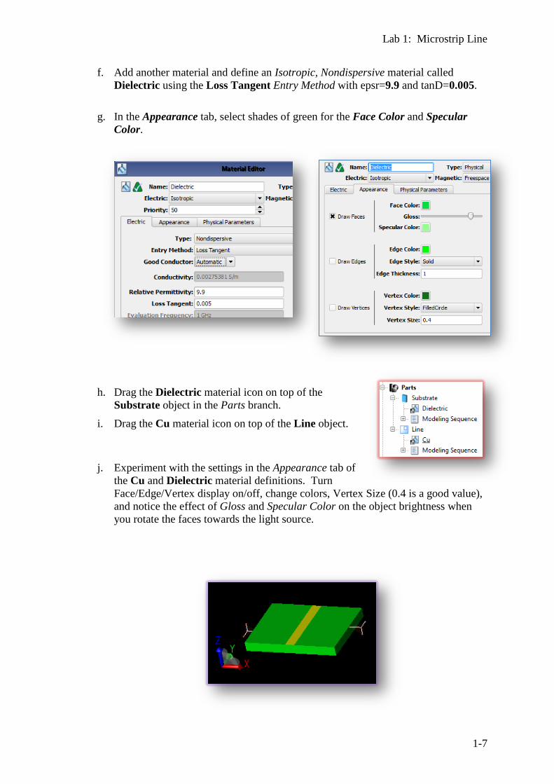
f. Add another material and define an Isotropic, Nondispersive material called Dielectric using the Loss Tangent Entry Method with epsr=9.9 and tanD=0.005.
g. In the Appearance tab, select shades of green for the Face Color and Specular Color.
h. Drag the Dielectric material icon on top of the Substrate object in the Parts branch.
i. Drag the Cu material icon on top of the Line object.
j. Experiment with the settings in the Appearance tab of the Cu and Dielectric material definitions. Turn Face/Edge/Vertex display on/off, change colors, Vertex Size (0.4 is a good value), and notice the effect of Gloss and Specular Color on the object brightness when you rotate the faces towards the light source.

Lab 1: Microstrip Line
1-8
4. Define the Outer Boundary Conditions
The outer boundary conditions on each of the six sides of the model space must be set to indicate how the EM simulators will interpret the space beyond them.
a. Double-click on the Simulation Domain > Boundary Conditions branch of the Project tree to open the Boundary Conditions Editor.
b. With the Lock all flag turned off, set the Lower Z boundary to PEC. This sets the bottom of the bounding box as a perfect conductor which will become the substrate ground plane.
c. Note the Absorption Type is greyed out because these only apply to FDTD.
d. Click Done.
5. Set Bounding Box Dimensions
a. Double-click the FEM Padding branch.
b. Set the lower and upper X- and Y-padding to 0 mm. The lower Z-padding must also be 0 mm to make sure the bottom PEC surface touches the bottom of the substrate. Set the upper Z-padding to 10 mm. Since the FEM absorbing boundary acts like a resistive surface if placed too close to a structure, we want to move it some multiple of the substrate thickness and line width away.

Lab 1: Microstrip Line
1-9
6. Define Waveguide Ports for FEM Simulation
a. Right-click on the Circuit Components/Ports branch and choose New Waveguide Port.
b. Click the Pick tool and then hover the mouse over the substrate face at Y = -7.5 mm and click to define the port. A transparent surface appears to indicate the port cross section that will be used by the FEM port solver.
c. On the Properties tab, change the name to Waveguide Port1 and select the 50 ohm Voltage Source for the Waveguide Port Definition. This will result in 50 Ohm S-Parameters (renormalized from the generalized S-Parameters using the Power/Current characteristic impedance computed by the port solver). If you were to choose the 1W Modal Power Feed instead, you would get the generalized S-Parameters instead.

Lab 1: Microstrip Line
1-10
d. Click the Impedance Lines tab. Define the line along which the voltage for the Zpv and Zvi characteristic impedances will be computed (the electric field for Mode 1 will be integrated along this line). Click the Endpoint 1 Pick tool and then click on the midpoint of the bottom substrate edge.
e. Click the Endpoint 2 Pick tool and then click on the midpoint of the strip edge. You could also type the coordinates directly.
f. Click Done.
g. Repeat the procedure for the 2nd port, changing the name to Waveguide Port2. You have to rotate the model to be able to select the opposite face.
h. Save the project.
Lab 1: Microstrip Line
1-11
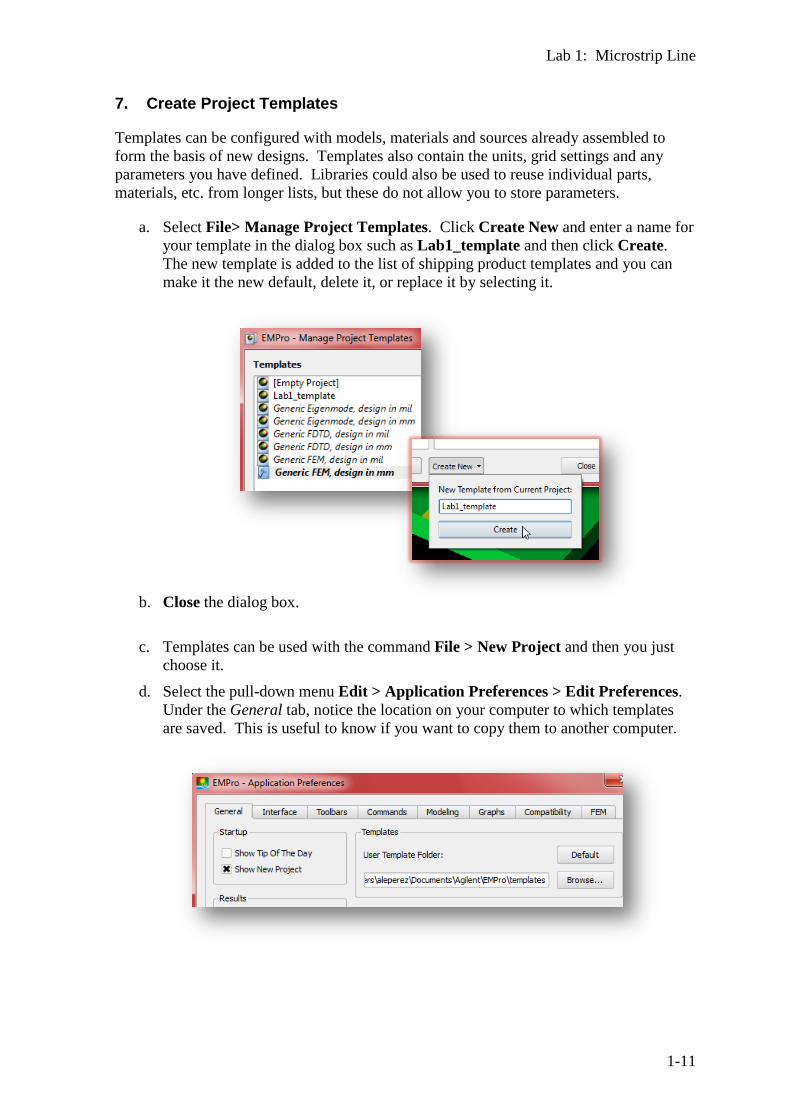
7. Create Project Templates
Templates can be configured with models, materials and sources already assembled to form the basis of new designs. Templates also contain the units, grid settings and any parameters you have defined. Libraries could also be used to reuse individual parts, materials, etc. from longer lists, but these do not allow you to store parameters.
a. Select File> Manage Project Templates. Click Create New and enter a name for your template in the dialog box such as Lab1_template and then click Create. The new template is added to the list of shipping product templates and you can make it the new default, delete it, or replace it by selecting it.
b. Close the dialog box.
c. Templates can be used with the command File > New Project and then you just choose it.
d. Select the pull-down menu Edit > Application Preferences > Edit Preferences. Under the General tab, notice the location on your computer to which templates are saved. This is useful to know if you want to copy them to another computer.

Lab 1: Microstrip Line
1-12
8. Run an FEM Simulation
a. Click on the Edit simulation setup button next to the FEM Simulation pull-down menu.
b. Keep the default adaptive frequency sweep from 1 GHz to 10 GHz with 20 Sample Points Limit. (Click the Parameters tab on the right to see the variable definitions which were created from the template chosen during project creation).
c. Click on the Mesh/Refinement Properties tab. Define a Delta error of 0.02, 3 minimum adaptive passes and 10 maximum adaptive passes.
d. Under the Solver tab, select the Direct matrix solver.
e. Click Create & Queue Simulation. The Simulations window opens (scroll for it if it is not visible). You will also see a mesh window popping up.

Lab 1: Microstrip Line
1-13
f. Under the Log tab, you can see entries for the refinement level, simulation frequency, mesh count, CPU and elapsed times for the mesher, matrix size in number of unknowns, memory consumption in GB, CPU and elapsed time for the matrix solver, and the DeltaS values compared to the desired Delta Error: (0.010[->0.020]). If Delta Error is met, the adaptive sweep proceeds with the previous to last mesh (~9500 unknowns – may vary from release to release due to algorithm changes).
9. View Results
a. Click on the Results tab. The top columns are data filters. You can right-click on the headers to change them, but the default ones are usually adequate. Click Frequency (swept data) under Domain and S-Parameters under Result Type. Note the data that appears in the list below.

Lab 1: Microstrip Line
1-14
b. Right-click any of the column titles in the bottom results list and check what’s available. Misc Info can be useful. The Results window column settings are saved across EMPro sessions, but can be reset using the application preference Clear Saved Layout Now.
c. Right-click on the entry for S21 and choose View (default).
d. Notice that an entry is created under the Graphs branch of the Project tree. Here you can rename, delete and open the graph.
e. Save the project.
Lab 1: Microstrip Line
1-15
10. Define Discrete Sources
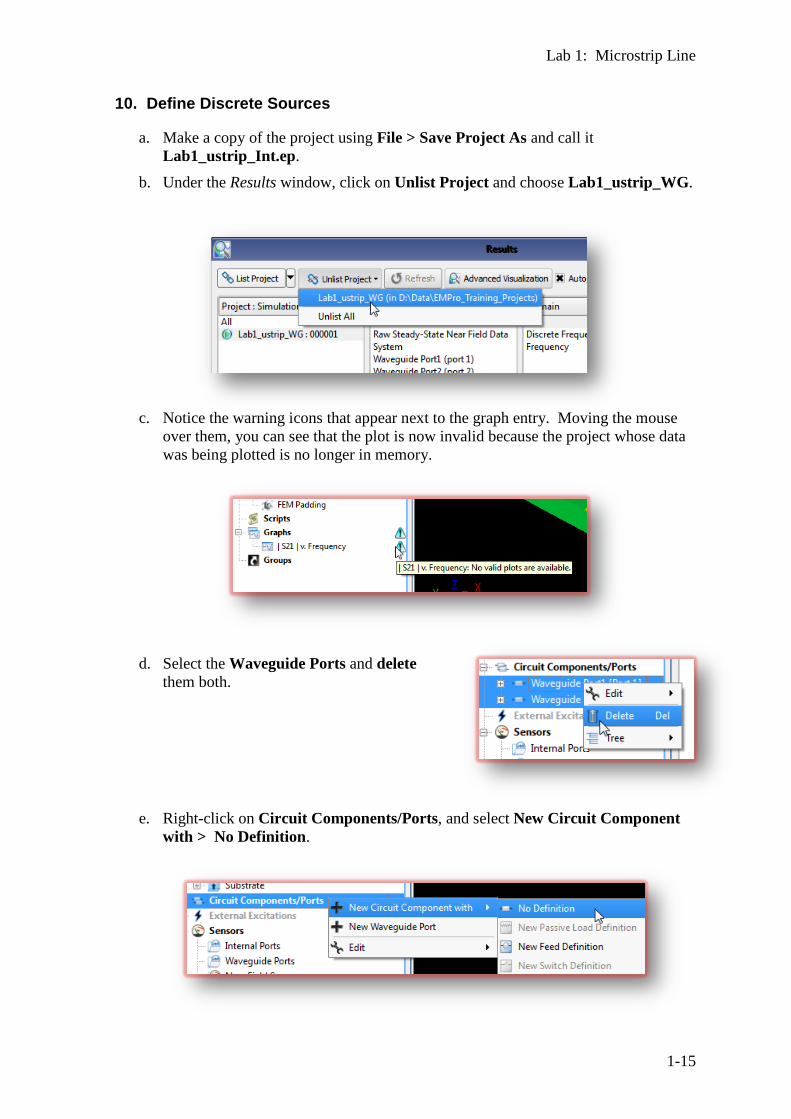
a. Make a copy of the project using File > Save Project As and call it Lab1_ustrip_Int.ep.
b. Under the Results window, click on Unlist Project and choose Lab1_ustrip_WG.
c. Notice the warning icons that appear next to the graph entry. Moving the mouse over them, you can see that the plot is now invalid because the project whose data was being plotted is no longer in memory.
d. Select the Waveguide Ports and delete them both.
e. Right-click on Circuit Components/Ports, and select New Circuit Component with > No Definition.

Lab 1: Microstrip Line
1-16
f. No new feed definition is needed because when you created the waveguide ports, two definitions were automatically created under the Circuit Component Definitions branch.
g. Select the Pick tool for the location of Endpoint 1. Position the mouse over the bottom substrate edge at Y =-7.5 mm. Click on the midpoint of the edge.
h. Select the Pick tool for Endpoint 2 and select the midpoint of the top microstrip edge. A cylinder on a line segment appears indicating the component location.
i. Click on the Properties tab and name the new component Port1. Select the 50 ohm Voltage Source for the Component Definition. The cylinder changes to an arrow indicating the feed polarity.

Lab 1: Microstrip Line
1-17
j. Click on the Extent tab. Select the flag Use Sheet. Change the first X-coordinate to -1 mm. This will form a rectangular sheet across which the impressed voltage will be fanned out to decrease the parasitic effect of this type of source.
k. Click Done.
l. To change the color of the components, click Edit > Application Preferences > Edit Preferences and select the Modeling tab. Pick a color so that you can see the components clearly.
m. Repeat the procedure to define Port2 at X=7.5 mm. Make sure the sheet only goes from X=1 mm to X=-1 mm. (You can use Parts Global Opacity to see through objects.)
n. Double-click the FEM Padding branch and edit the Y-padding to be 5 mm in both directions. Voltage sources are not allowed to touch an outer boundary.
o. Save the new project.

Lab 1: Microstrip Line
1-18
11. Simulate using FEM
a. Click the Simulate button.
b. Check the Log tab under the Simulation window.
12. Compare the Results
a. Click the Results tab.
b. Use the List Project button to reload the simulation results for Lab1_ustrip_WG.
c. Right-click S21 from Lab1_ustrip_Int and choose Create Line Graph.
d. Choose the existing |S21| v. Frequency Target Graph.

Lab 1: Microstrip Line
1-19
e. The results are further apart at higher frequencies due to the parasitic effect of the voltage sources. Click the Legend Visible toggle a couple times.
f. From the Results window, choose S21 from the two simulations using the Ctrl key, and right-click Create Line Graph. Then select Phase.
g. Click on the Graph Properties icon. On the left, click the Axes Properties tab. Edit the Min/Max phases to go from -200 to +200 degrees.

Lab 1: Microstrip Line
1-20
h. The phase response matches reasonably well. Re-run the simulation turning off the Use Sheet flags under the Ports definitions. The impact due to the source parasitics is more pronounced.

Lab 1: Microstrip Line
1-21
13. Define the FDTD Source and Grid
a. Use File > Save Project As to create Lab1_ustrip_FDTD. Turn on the FDTD Simulation user interface skin.
b. Hover the mouse cursor over the warning messages inside the Circuit Component Definitions branch – the 1 W Modal Power Feed is not valid in FDTD. Delete it. The 50 ohm Voltage Source requires a time-domain waveform. The ports are also invalid as a result of the missing waveform.
c. To view the feed properties, double-click the 50 ohm Voltage Source entry under Circuit Component Definitions. The 1 Volt excitation with a 50 Ohm source resistance is the typical source used for FDTD simulations, but a waveform must be assigned to this feed.
d. Click Done.
e. Right-click on Waveforms and choose New Waveform Definition. Double-click the new Automatic waveform and take a look. Cancel.
Lab 1: Microstrip Line
1-22
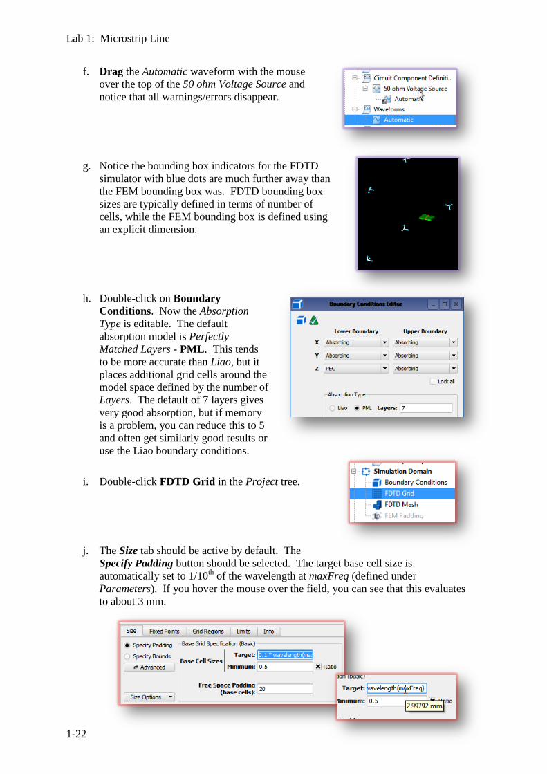
f. Drag the Automatic waveform with the mouse over the top of the 50 ohm Voltage Source and notice that all warnings/errors disappear.
g. Notice the bounding box indicators for the FDTD simulator with blue dots are much further away than the FEM bounding box was. FDTD bounding box sizes are typically defined in terms of number of cells, while the FEM bounding box is defined using an explicit dimension.
h. Double-click on Boundary Conditions. Now the Absorption Type is editable. The default absorption model is Perfectly Matched Layers - PML. This tends to be more accurate than Liao, but it places additional grid cells around the model space defined by the number of Layers. The default of 7 layers gives very good absorption, but if memory is a problem, you can reduce this to 5 and often get similarly good results or use the Liao boundary conditions.
i. Double-click FDTD Grid in the Project tree.
j. The Size tab should be active by default. The Specify Padding button should be selected. The target base cell size is automatically set to 1/10th of the wavelength at maxFreq (defined under Parameters). If you hover the mouse over the field, you can see that this evaluates to about 3 mm.

Lab 1: Microstrip Line
1-23
k. Click Advanced to define different padding values in different directions. . Define Free Space Padding as 5 in both X- and Y-directions (side walls will be 3 mm*5=15 mm away). Set the Lower Z padding to 0 and the Upper Z padding to 10 cells (top wall will be 3 mm*10=30 mm away).
l. Press Done to close the Editing Grid dialog.
m. Right-click on the Substrate object in the Geometry window or on its name in the Project tree, and select Gridding/Meshing > FDTD Gridding Properties.
n. Select Use Automatic Grid Regions and click Advanced and change the Z-directed Target to 0.5 mm. It is generally recommended that substrates are meshed with at least 3 cells along their height for better accuracy.
The Target base cell size is the maximum value a cell in that direction can have. A cell may be smaller than this size but only as small as the Minimum allows. Geometric features smaller than this will not be resolved.
14. Creating the FDTD Mesh
The mesh is created as soon as we activate the mesh view. The grid is a set of brick-shaped elements that is superimposed on the geometry. The cell edges do not necessarily terminate at object boundaries depending on how you define the grid properties. The material properties of the geometric objects are mapped to the grid edges to define the simulation mesh for the FDTD solver.
a. Drag the object Line in the Parts list above the object Substrate. (Note: This step is only needed until materials priority is implemented in EMPro 2012.06.)

Lab 1: Microstrip Line
1-24
b. Double-click on the FDTD Mesh branch in the Project tree or click the mesh toggle icon on the right.
c. Select 3D Mesh on the bottom left of the Geometry window and then select Faces With Edge and rotate the geometry. Turn Parts and Component visibility off.
d. If you notice “holes” in the mesh under the microstrip, don’t worry about these. In FDTD, the faces cannot be drawn in a meaningful manner when edges of that face have different materials assigned to them. Only the edges of the cells are used in the simulation. To see what FDTD actually sees in a simulation, turn on All Edges.
e. Toggle the Component Visibility icon along the right of the Geometry window (also works for waveguide surfaces). This will let you see the centered component definition vs. the actual cell edge where the feed is applied during the simulation (use External Edges Only display mode). If you have a component selected in the Project tree, then it will be visible regardless of this setting. You need to select something else to make it invisible.
f. Select the “Back (+Y)” view from the View Tools icon.

Lab 1: Microstrip Line
1-25
g. Select the Mesh Cutplanes button. Click the ZX Plane at Y-slice = 6 in order to view the slice of the mesh where Port1 is located. The cell edges above and below the voltage feed have been automatically converted to a PEC wire along the length of the feed to make sure that the voltage is actually applied between the ground plane and the microstrip.
h. Rotate the view and try different cuts and planes using the visibility controls (some of which require you to turn the Parts visible to work).
i. When finished, dismiss the mesh controls by clicking on the mesh icon or by double-clicking the FDTD Mesh branch of the Project tree.
j. Save the project.
15. Setting Up the FDTD Simulation
a. Click the Edit simulation setup icon.
b. Click on the Setup S-Parameters tab. Enable S-Parameters is on by default. Leave Port1 as the only active port. This will give us S11 and S21. Enabling the other port would require a 2nd simulation.

Lab 1: Microstrip Line
1-26
c. Click on the Specify Termination Criteria tab. The default values are sufficient for a large class of problems. The simulation will stop if the convergence of -30 dB has been reached or after a maximum of 50,000 time steps has been simulated.
d. Select Create & Queue Simulation to run this simulation.
e. Click on the Log tab to see the simulation progress.
f. View the Summary tab to see the Timestep and Maximum resolvable frequency.

Lab 1: Microstrip Line
1-27
16. Viewing the Results
FDTD simulation results can be viewed dynamically even before a simulation completes. S-Parameter graphs update automatically as the simulation progresses.
a. Click on the Results tab along the right edge of the EMPro window.
NOTE: Perform the next two steps only if you skipped the FEM part of the lab above.
b. Notice the 4 columns at the top. These can be customized and are used to filter the data available for plotting. Right-click on the column headers and select different filters to familiarize yourself with the choices.
c. The columns at the bottom are the actual data which you can sort, select and plot. Here too, right-click on the column headers to see the choices.
d. Double-click on S[2,1] of the FDTD simulation for the default graph.

Lab 1: Microstrip Line
1-28
e. If you performed the FEM part of the lab, right-click on S21 and using Create Line Graph add it to the FEM S21 plot. The parasitic effect of the FDTD feed is even more pronounced than for a FEM line source (at least using this coarse mesh).
f. Take a look at the marker tools and choose Point Marker to read off some values on the trace. Notice that if you click on a point, the marker readout and a reference dot will be placed on the graph.
g. Try some of the other markers as well.

Lab 1: Microstrip Line
1-29
17. Saving Parts in a Library
One useful feature of EMPro is the ability to easily generate libraries of any of the items created in a project. Earlier you saw the idea of templates, but there, all saved items are added to a new project. With libraries, only the items you want can be selected dynamically.
a. From the right side of the Main window, select the Libraries tab.
b. Click File > New Library > EMPro Library. Select Browse Folders, and create a new folder using the right mouse button called EMPro_Libraries in the hpeesof folder in your EMPro startup directory (e.g., C:\users\default or wherever your EMPro projects are created by default). Name the new library MaterialLibrary.
c. Open the Definitions branch. From the Project tree in the Main window, select both Cu and Dielectric and drag them on top of any entry in the Libraries window. These materials will now be available by default in all other EMPro projects. Even if you use File > Remove Library, the library will not be deleted from disk.
d. Close the Libraries window.
Your EMPro Home Folder

Lab 1: Microstrip Line
1-30
18. Application Preferences
a. Select Edit > Application Preferences > Edit Preferences. The Transparency Algorithm can be quite useful when trying to visualize models with overlapping 3D shapes when you use the Opacity setting next to the Object Visibility toggle. The Text Color is used for the on-screen text readouts for bounding box sizes, etc. Under the Commands tab, you can define keyboard shortcuts and change the toolbar icons dynamically by just dragging a command to a toolbar or drag an icon away from a toolbar to remove it. For example, define “P” to bring up this dialog.
b. Click on the Modeling tab. Here you can set the default colors used to display faces, edges, and/or vertices for parts when they are first created. You can also set the color of the components (like voltage sources) and Geometry window background color. Press OK when done experimenting with the settings potentially of interest to you.
c. Use Edit > Application Preferences > Export Preferences or Import to back them up or share them with other users.
End of Lab Exercises