ksz9563rnx hardware design checklist
TRANSCRIPT

KSZ9563RNXHardware Design Checklist
1.0 INTRODUCTION
This document provides a hardware design checklist for the KSZ9563RNX. These checklist items should be followed when utilizing the KSZ9563RNX in a new board design.
A summary of the hardware design checklist items is provided in Section 13.0, "Hardware Checklist Summary," on page 32. Detailed information for each checklist item can be found in the following corresponding sections:
• Package and Pin Considerations on page 2
• Reference Clock Circuits and Connections on page 3
• Power/Ground Connections on page 5
• ISET Resistor on page 6
• Ethernet PHY Ports on page 6
• Management Bus Selection
• MAC Port 3 - Digital Data Bus Interfaces on page 17
• LED Indicator Pins on page 29
• GPIO Pins on page 31
• Miscellaneous on page 31
A listing of available KSZ9563RNX hardware design collaterals can be found in Section 12.0, "Reference Materials," on page 31.
2018 Microchip Technology Inc. DS00002770A-page 1

KSZ9563RNX
2.0 PACKAGE AND PIN CONSIDERATIONS
2.1 Package Orientation and Pin Numbering
Check to ensure that the package orientation and pin numbering with respect to the top view of the package are in the counterclockwise direction. Refer to the KSZ9563RNX Data Sheet for additional information.
2.2 Pin Type
Check the pinouts of the KSZ9563RNX device to ensure all pin types and directions match the KSZ9563RNX DataSheet and the interfacing devices are configured with corresponding input, output, or bidirectional pin types for sche-matic design rule error checking.
It is important to always check the pin types in the data sheet of the connecting pins between two devices to ensure the adjoining pins are not both inputs and not both outputs. Do not rely on just the pin name of the bus interface between two connecting devices. The same pin name may be defined as an input or an output depending on the interface per-spective. This is especially for the RGMII, RMII, and MII pins, as defined from the PHY perspective or MAC perspective.
2.3 Configuration Strap Pins
The KSZ9563RNX utilizes configuration strap pins to configure the device for different modes. These strap pins are con-figured by using internal and external pull-up/pull-down resistors to create a high or low state on the pins that are sam-pled at the end of a device power-up or software reset cycle. They are also latched when powering-up from a hardware or software power-down or Hardware Reset state (rising edge of RESET_N).
In some systems, for example, the connecting MAC input pins may drive high during power-up or reset and conse-quently cause the multiplexed strap-in pins on the RGMII/RMII/MII signals to be latched high, instead of low. In this case, it is recommended to add 1k pull-downs to these strap-in pins to ensure they latch low.
Check to ensure proper external pull-ups or pull-downs, as needed, are installed for all the strap pins, as defined in the KSZ9563RNX Data Sheet.
DS00002770A-page 2 2018 Microchip Technology Inc.

KSZ9563RNX
3.0 REFERENCE CLOCK CIRCUITS AND CONNECTIONS
A crystal or external clock source can be used to generate the 25 MHz reference clock for the device.
3.1 Crystal Circuit
The following notes for the crystal circuit refer to Figure 3-1.
• A 25.000 MHz (±50 ppm) crystal is recommended. Refer to the latest revision of the KSZ9563RNX Data Sheet.
• XI (pin 58) is the crystal circuit input. This pin connects to one side of the crystal and also connects to a capacitor to ground.
• XO (pin 57) is the clock circuit output. This pin connects to the other side of the crystal, as well as a capacitor to ground.
• The external capacitor value for the crystal can vary and depends on the CL specifications of the selected crystal and the stray capacitance of the PCB traces.
• The selected crystal and PCB design and layout contribute to the performance of the crystal circuit. Once the board is brought up and is operational, a check for frequency accuracy and stability across the system operating conditions is recommended.
FIGURE 3-1: CRYSTAL CIRCUIT
25MHz Crystal±50 ppm
C1
C2
XI
XO
58
57
2018 Microchip Technology Inc. DS00002770A-page 3

KSZ9563RNX
3.2 External Clock Source/Oscillator Circuit
The following notes for the external clock/oscillator circuit refer to Figure 3-2.
• An external 25.000 MHz (±50 ppm) clock source, such as an oscillator, with a Total Period Jitter (peak-to-peak) of less than 100 ps is recommended. Refer to the latest version of the KSZ9563RNX Data Sheet.
• XI (pin 58) is the input for the external clock source. A 22-50 series source termination at the clock output pin is recommended.
• XO (pin 57) is a no connect.
• The external clock source should reference the AVDDH voltage level supplied to the KSZ9563RNX device.
FIGURE 3-2: EXTERNAL CLOCK SOURCE/OSCILLATOR CIRCUIT
XI
XONC
25MHz Oscillator±50 ppm
AVDDH = 3.3V or 2.5V
58
57
AVDDH
DS00002770A-page 4 2018 Microchip Technology Inc.

KSZ9563RNX
4.0 POWER/GROUND CONNECTIONS
4.1 Power and Ground Block Diagram
The power and ground connections are shown in Figure 4-1.
FIGURE 4-1: POWER AND GROUND CONNECTIONS
0.1μF
22μF 26
38
54
8
19
61
5
11
16
56
64
20
34
37
41
51
55
E-pad(exposed pad)
VDDIO +1.8V, 2.5V or 3.3V
AVDDH+2.5V or 3.3V
DVDDL+1.2V
0.1μF
0.1μF
0.1μF
0.1μF
0.1μF
0.1μF
22μF
0.1μF
0.1μF
0.1μF
0.1μF
0.1μF
0.1μF
22μF
0.1μF
0.1μF
0.1μF
0.1μF
22μF
59
AVDDL+1.2V
4.1.1 POWER PINS
The following notes for the power pins and their connections refer to Figure 4-1.
• VDDIO powers the digital I/O pins and can operate at either +3.3V, +2.5V, or +1.8V.• AVDDH powers the analog transceiver, can operate at either +3.3V or +2.5V for reduced power consumption, and
should have a series ferrite bead placed between board power supply to provide further filtering.• DVDDL powers the digital core and operates at +1.2V.• AVDDL powers the analog core and operates at +1.2V. If a single 1.2V board supply is used, a series ferrite bead
should be placed between the DVDDL power and the AVDDL power to provide further filtering.• Each power pin requires a 0.1 µF decoupling capacitor. These capacitors should be placed as close as possible to
the power pins without using vias.• The ferrite bead is typically 100-220Ω (at 100 MHz).• A bulk capacitor should be placed on each power rail near the device. These capacitors should have a typical
capacitance value of 22 µF and an Equivalent Series Resistance (ESR) of no more than 1.0Ω. Microchip recom-mends a very low ESR ceramic capacitor for design stability.
• All four power rails (VDDIO, AVDDH, DVDDL, and AVDDL) should each have less than 50 mVp-p ripple.
2018 Microchip Technology Inc. DS00002770A-page 5

KSZ9563RNX
4.1.2 GROUND PIN AND EXPOSED PAD
The following notes for the ground pin, the exposed pad ground, and their connections refer to Figure 4-1.
• Ground pin 59 should connect directly to the solid ground plane on the board.
• Exposed pad (E-pad) ground on the bottom side of the chip should connect directly to the solid ground plane on the board. See the device data sheet for the E-pad dimensions, recommended land pattern, and thermal via size and number requirements.
• All ground connections, ground pin 59 and the E-pad, should tie directly together to the same ground plane. Sep-arate ground planes are not recommended.
5.0 ISET RESISTOR
The ISET pin of the KSZ9563RNX should connect to signal ground through a 6.04 kΩ 1.0% resistor. The resistor value sets the bias currents to generate the 10BASE-T/100BASE-TX/1000BASE-T transmit signal swing.
Some design guidelines for the ISET resistor:
• Place the resistor close to the ISET pin of device.
• Do not place any capacitor in parallel with the ISET resistor.
• Route all signals, especially clocks and high frequency signals, away from this pin to avoid coupling.
• Do not share the ISET resistor ground via with any other component’s grounding via.
6.0 ETHERNET PHY PORTS
6.1 Ethernet Signal Pins
The KSZ9563RNX has Voltage-mode transmit drivers and on-chip terminations for its PHY differential pairs. No external termination is required for the four differential pairs for the two PHY ports.
The following are the PHY port 1 differential signals:
• TXRX1P_A (pin 62): This pin is the PHY port 1 differential pair A twisted pair positive connection. It is used for 10BASE-T/100BASE-TX/1000BASE-T speeds and connects the internal PHY to the external 10/100/100 magnet-ics.
• TXRX1M_A (pin 63): This pin is the PHY port 1 differential pair A twisted pair negative connection. It is used for 10BASE-T/100BASE-TX/1000BASE-T speeds and connects the internal PHY to the external 10/100/1000 mag-netics.
• TXRX1P_B (pin 1): This pin is the PHY port 1 differential pair B twisted pair positive connection. It is used for 10BASE-T/100BASE-TX/1000BASE-T speeds and connects the internal PHY to the external 10/100/1000 mag-netics.
• TXRX1M_B (pin 2): This pin is the PHY port 1 differential pair B twisted pair negative connection. It is used for 10BASE-T/100BASE-TX/1000BASE-T speeds and connects the internal PHY to the external 10/100/1000 mag-netics.
• TXRX1P_C (pin 3): This pin is the PHY port 1 differential pair C twisted pair positive connection. It is used for 1000BASE-T speed only and connects the internal PHY to the external 1000 magnetics. For 10BASE-T/100BASE-TX speeds only, this pin can be left as a no connect.
• TXRX1M_C (pin 4): This pin is the PHY port 1 differential pair C twisted pair negative connection. It is used for 1000BASE-T speed only and connects the internal PHY to the external 1000 magnetics. For 10BASE-T/100BASE-TX speeds only, this pin can be left as a no connect.
• TXRX1P_D (pin 6): This pin is the PHY port 1 differential pair D twisted pair positive connection. It is used for 1000BASE-T speed only and connects the internal PHY to the external 1000 magnetics. For 10BASE-T/100BASE-TX speeds only, this pin can be left as a no connect.
• TXRX1M_D (pin 7): This pin is the PHY port 1 differential pair D twisted pair negative connection. It is used for 1000BASE-T speed only and connects the internal PHY to the external 1000 magnetics. For 10BASE-T/100BASE-TX speeds only, this pin can be left as a no connect.
DS00002770A-page 6 2018 Microchip Technology Inc.

KSZ9563RNX
The following are the PHY port 2 differential signals:
• TXRX2P_A (pin 9): This pin is the PHY port 2 differential pair A twisted pair positive connection. It is used for 10BASE-T/100BASE-TX/1000BASE-T speeds and connects the internal PHY to the external 10/100/100 magnet-ics.
• TXRX2M_A (pin 10): This pin is the PHY port 2 differential pair A twisted pair negative connection. It is used for 10BASE-T/100BASE-TX/1000BASE-T speeds and connects the internal PHY to the external 10/100/1000 mag-netics.
• TXRX2P_B (pin 12): This pin is the PHY port 2 differential pair B twisted pair positive connection. It is used for 10BASE-T/100BASE-TX/1000BASE-T speeds and connects the internal PHY to the external 10/100/1000 mag-netics.
• TXRX2M_B (pin 13): This pin is the PHY port 2 differential pair B twisted pair negative connection. It is used for 10BASE-T/100BASE-TX/1000BASE-T speeds and connects the internal PHY to the external 10/100/1000 mag-netics.
• TXRX2P_C (pin 14): This pin is the PHY port 2 differential pair C twisted pair positive connection. It is used for 1000BASE-T speed only and connects the internal PHY to the external 1000 magnetics. For 10BASE-T/100BASE-TX speeds only, this pin can be left as a no connect.
• TXRX2M_C (pin 15): This pin is the PHY port 2 differential pair C twisted pair negative connection. It is used for 1000BASE-T speed only and connects the internal PHY to the external 1000 magnetics. For 10BASE-T/100BASE-TX speeds only, this pin can be left as a no connect.
• TXRX2P_D (pin 17): This pin is the PHY port 2 differential pair D twisted pair positive connection. It is used for 1000BASE-T speed only and connects the internal PHY to the external 1000 magnetics. For 10BASE-T/100BASE-TX speeds only, this pin can be left as a no connect.
• TXRX2M_D (pin 18): This pin is the PHY port 2 differential pair D twisted pair negative connection. It is used for 1000BASE-T speed only and connects the internal PHY to the external 1000 magnetics. For 10BASE-T/100BASE-TX speeds only, this pin can be left as a no connect.
6.2 Magnetics Selection
A 1:1 isolation transformer is required at the line interface. For designs exceeding FCC requirements, utilize one with integrated Common-mode chokes. An optional auto-transformer stage following the chokes provides additional Com-mon-mode noise and signal attenuation.
A magnetic with symmetrical and identical circuits for all four differential pairs is recommended for Auto MDI/MDI-X sup-port.
Table 6-1 provides a list of recommended magnetic characteristics. Check to ensure selected magnetics meet or exceed these requirements.
TABLE 6-1: MAGNETICS SELECTION CRITERIA
Parameter Value Test Condition
Turns ratio 1 CT:1 CT —
Open-circuit inductance (min.) 350 µH 100 mV, 100 kHz, 8 mA
Insertion loss (typ.) 1.0 dB 100 kHz to 100 MHz
HIPOT (min.) 1500 Vrms —
2018 Microchip Technology Inc. DS00002770A-page 7

KSZ9563RNX
6.3 Magnetic and RJ45 Plug Connections
6.3.1 10/100/1000 MBPS (GIGABIT) ETHERNET
The Ethernet signal connections between the KSZ9563RNX device and magnetics, and between the magnetics and the RJ45 connector are shown in Figure 6-1 for Gigabit Ethernet support.
FIGURE 6-1: GIGABIT ETHERNET CONNECTIONS
1
2
3
7
8
4
5
6
4X 75 Ohm
1000 pF / 2kV
CHASSIS GROUND
(4X 0.1uF)
TXRXxP_A
TXRXxM_A
TXRXxP_B
TXRXxM_B
TXRXxP_C
TXRXxM_C
TXRXxP_D
TXRXxM_D
SIGNAL GROUND
With the Voltage-mode implementation, the KSZ9563RNX transmit drivers supply the Common-mode voltages to the four differential pairs.
On the KSZ9563R chip side, each of the four transformer center tap pins should not be connected to any power supply source on the board. Instead, the center tap pins should be separated from one another and connected through sepa-rate 0.1 µF Common-mode capacitors to ground. Separation is required because the Common-mode voltage could be different between the differential pairs, depending on the operating mode.
On the RJ45 connector side, each of the four transformer center tap pins is terminated through separate 75Ω resistors that are joined together through a single 1000 pF, 2 kV capacitor to chassis ground. And the metal case shield of the RJ45 connector is tied directly to chassis ground.
The Ethernet signal mappings across the magnetics between the KSZ9563RNX device and the RJ45 connector are shown in Table 6-2 for Gigabit Ethernet support.
DS00002770A-page 8 2018 Microchip Technology Inc.

KSZ9563RNX
TABLE 6-2: KSZ9563RNX/RJ45 CONNECTOR MAPPING - GIGABIT ETHERNET
KSZ9563RNX Pinout RJ45 Connector Pinout
TXRXxP_A Pin 1
TXRXxM_A Pin 2
TXRXxP_B Pin 3
TXRXxM_B Pin 6
TXRXxP_C Pin 4
TXRXxM_C Pin 5
TXRXxP_D Pin 7
TXRXxM_D Pin 8
6.3.2 10/100 MBPS (FAST) ETHERNET ONLY
For applications that require a link-up limited to 10/100 Mbps speeds only, the Auto-Negotiation advertisement for 1000Mbps speed and full-/half-duplex capabilities should be removed to avoid any potential link-up issue because of interop-erability. After power-up or reset, program the following 16-bit Port N register bit settings, where N is 1 for port 1, and 2 for port 2.
1. Set Port Register 0xN100, Bit [6] = ‘0’ to remove 1000 Mbps speed.
2. Set Port Register 0xN112, Bits [9:8] = ‘00’ to remove Auto-Negotiation advertisements for 1000 Mbps full-/half-duplex.
3. Write a ‘1’ to Register 0xN100, Bit [9], a self-clearing bit, to force a restart of Auto-Negotiation.
2018 Microchip Technology Inc. DS00002770A-page 9

KSZ9563RNX
6.3.2.1 10/100 Mbps Ethernet (MDI Mode)
The Ethernet signal connections between the KSZ9563RNX device and magnetics, and between the magnetics and the RJ45 connector are shown in Figure 6-2 for Fast Ethernet support for the MDI mode configuration.
FIGURE 6-2: FAST ETHERNET MAGNETIC CONNECTIONS (MDI MODE)
1
2
3
7
8
4
5
6
4X 75 Ohm
1000 pF / 2kV
CHASSIS GROUND
(2X 0.1uF)
TXRXxP_A
TXRXxM_A
TXRXxP_B
TXRXxM_B
TXRXxP_C
TXRXxM_C
TXRXxP_D
TXRXxM_D
SIGNAL GROUND
Note: Despite having the Auto MDI/MDI-X function to swap differential pairs, PHY ports that are implemented as Ethernet end devices are connected by default to the MDI mapping with differential pairs A and B mapped to RJ45 connector pin pairs (1, 2) and (3, 6), respectively.
With the Voltage-mode implementation, the KSZ9563RNX transmit drivers supply the Common-mode voltages to the four differential pairs (two active: pairs A and B; and two inactive: pairs C and D for 10/100-Mbps Speed modes).
On the KSZ9563R chip side:
• The two transformer center tap pins, for the active differential pairs A and B, should not be connected to any power supply source on the board. Instead, the center tap pins should be separated from one another and con-nected through separate 0.1 µF Common-mode capacitors to ground. Separation is required because the Com-mon-mode voltage could be different between the differential pairs, depending on the operating mode.
• Auto-Negotiation and 10BASE-T/100BASE-TX speeds use only differential pairs A and B. The inactive (unused) differential pairs C and D are left as no connects.
DS00002770A-page 10 2018 Microchip Technology Inc.

KSZ9563RNX
On the RJ45 connector side:
• The two transformer center tap pins, for the active differential pairs A and B, are terminated through separate 75Ω resistors that are joined together with the other two separate 75Ω resistors (in the following bullet point) through a single 1000 pF, 2 kV capacitor to chassis ground.
• The unused RJ45 pins are shorted together as pin pairs (4, 5) and (7,8) and terminated through separate 75Ω resistors that are joined together with the other two separate 75Ω resistors (in the previous bullet point) through the same single 1000 pF, 2 kV capacitor (in the previous bullet point) to chassis ground.
• The metal case shield of the RJ45 connector is tied directly to chassis ground.
The Ethernet signal mappings across the magnetics between the KSZ9563RNX device and the RJ45 connector are shown in Table 6-3.
TABLE 6-3: KSZ9563RNX/RJ45 CONNECTOR MAPPING - FAST ETHERNET (MDI MODE)
KSZ9563RNX Pinout RJ45 Connector Pinout
TXRXxP_A Pin 1
TXRXxM_A Pin 2
TXRXxP_B Pin 3
TXRXxM_B Pin 6
2018 Microchip Technology Inc. DS00002770A-page 11

KSZ9563RNX
6.3.2.2 10/100 Mbps Ethernet (MDI-X Mode)
The Ethernet signal connections between the KSZ9563RNX device and magnetics, and between the magnetics and the RJ45 connector are shown in Figure 6-3 for Fast Ethernet support for the MDI-X mode configuration.
FIGURE 6-3: FAST ETHERNET MAGNETIC CONNECTIONS (MDI-X MODE)
1
2
3
7
8
4
5
6
4X 75 Ohm
1000 pF / 2kV
CHASSIS GROUND
(2X 0.1uF)
TXRXxP_A
TXRXxM_A
TXRXxP_B
TXRXxM_B
TXRXxP_C
TXRXxM_C
TXRXxP_D
TXRXxM_D
SIGNAL GROUND
Note: Despite having the Auto MDI/MDI-X function to swap differential pairs, PHY ports that are implemented as Ethernet midspan devices are connected by default to the MDI-X mapping with differential pairs A and B mapped to RJ45 connector pin pairs (3, 6) and (1, 2), respectively.
With the Voltage-mode implementation, the KSZ9563RNX transmit drivers supply the Common-mode voltages to the four differential pairs (two active: pairs A and B; and two inactive: pairs C and D for 10/100-Mbps Speed modes).
On the KSZ9563R chip side:
• The two transformer center tap pins, for the active differential pairs A and B, should not be connected to any power supply source on the board. Instead, the center tap pins should be separated from one another and con-nected through separate 0.1 µF Common-mode capacitors to ground. Separation is required because the Com-mon-mode voltage could be different between the differential pairs, depending on the operating mode.
• Auto-Negotiation and 10BASE-T/100BASE-TX speeds use only differential pairs A and B. The inactive (unused) differential pairs C and D are left as no connects.
DS00002770A-page 12 2018 Microchip Technology Inc.

KSZ9563RNX
On the RJ45 connector side:
• The two transformer center tap pins, for the active differential pairs A and B, are terminated through separate 75Ω resistors that are joined together with the other two separate 75Ω resistors (in the following bullet point) through a single 1000 pF, 2 kV capacitor to chassis ground.
• The unused RJ45 pins are shorted together as pin pairs (4, 5) and (7,8) and terminated through separate 75Ω resistors that are joined together with the other two separate 75Ω resistors (in the previous bullet point) through the same single 1000 pF, 2 kV capacitor (in the previous bullet point) to chassis ground.
• The metal case shield of the RJ45 connector is tied directly to chassis ground.
The Ethernet signal mappings across the magnetics between the KSZ9563RNX device and RJ45 connector are shown in Table 6-4.
FIGURE 6-4: KSZ9563RNX/RJ45 CONNECTOR MAPPING - FAST ETHERNET (MDI-X MODE)
KSZ9563RNX Pinout RJ45 Connector Pinout
TXRXxP_A Pin 3
TXRXxM_A Pin 6
TXRXxP_B Pin 1
TXRXxM_B Pin 2
2018 Microchip Technology Inc. DS00002770A-page 13

KSZ9563RNX
7.0 MANAGEMENT BUS SELECTION
For the selected management bus interface in the following sub-sections, check to ensure the listed design guidelines are followed. Also, refer to the application note, AN2661 “Getting Started with 3-Port Gigabit Ethernet Switch Configu-ration Options”, for further details.
7.1 SPI Slave Management
The SPI Slave Management mode provides complete read and write access to all KSZ9563RNX device (PHY and Switch) registers. The external SPI master device supplies the chip select (SCS_N), serial clock (SCL), and serial input data (SDI). Serial output data (SDO) is driven by the KSZ9563RNX.
To select and enable SPI Slave mode, the RXD1 and RXD0 strap pins are set to 1 and x (either 1 or 0), respectively, Refer to Section 2.3, Configuration Strap Pins for more details.
Voltage translators are needed if the VDDIO voltages of the KSZ9563RNX device and the external SPI master device are different.
The SPI block diagram and pin connections between the KSZ9563RNX device and the microcontroller (MCU) are shown in Figure 7-1.
FIGURE 7-1: SPI BLOCK DIAGRAM
VDDIO
Strap pins to enable SPI Slave Mode
RXD1 = 1
RXD0 = x (1 or 0)
MCU(SPI Master)
CS
SCL
MOSI
MISO
SCL
SDO
SDI
SCS_N
RXD1KSZ9563(SPI Slave)
RXD0
VDDIO
4.7K
VDDIO
7.2 I2C Slave Management
The I2C Slave Management mode provides complete read and write access to all KSZ9563RNX device (PHY and Switch) registers. The external I2C master device supplies the serial clock (SCL). The serial data (SDA) is a bidirectional open-drain that is driven by the I2C master for register read and write access and is driven by the KSZ9563RNX device to return the register read value.
To select and enable I2C Slave mode, the RXD1 and RXD0 strap pins are set to 0 and 1, respectively, Refer to Section 2.3, Configuration Strap Pins for more details.
An external 1.0-4.7 kΩ pull-up resistor is required on the SDA signal.
Voltage translators are needed if the VDDIO voltages of the KSZ9563RNX device and external I2C master device are different.
The I2C block diagram and pin connections between the KSZ9563RNX device and the microcontroller (MCU) are shown in Figure 7-2.
DS00002770A-page 14 2018 Microchip Technology Inc.

KSZ9563RNX
FIGURE 7-2: I2C BLOCK DIAGRAM
VDDIO
Strap pins to enable I2C Slave Mode
RXD1 = 0
RXD0 = 1
MCU(I2C Master)
SCL
SDA
SCL
SDA
RXD1
KSZ9563RNX(I2C Slave)RXD0
VDDIO
4.7K
VDDIO
1.0 - 4.7K
VDDIO
1.0K
7.3 In-Band Access (IBA) Management
In-Band Access (IBA) Management is a proprietary feature that uses customized 64-byte Ethernet frames to provide complete read and write access to all KSZ9563RNX device (PHY and Switch) registers. Any one of the three data ports (PHY port 1, PHY port 2, or MAC port 3) can be used for in-band register access.
To select and enable IBA Management mode, the LED1_1 strap pin is pulled low. Refer to Section 2.3, Configuration Strap Pins for more details. With the IBA pin strapping, PHY port 1 is assigned as the default IBA port. SPI or I2C man-agement is required to enable MAC port 3 (host processor port) or PHY port 2 (alternative PHY port) as the IBA port.
Refer to the In-Band Management (IBA) Control Register at address locations 0x0104 - 0x0107 in the KSZ9563RNX Data Sheet for the bit settings to select MAC port 3 or PHY port 2 as the IBA port.
Figure 7-3 shows the IBA block diagram.
FIGURE 7-3: IBA BLOCK DIAGRAM
KSZ9563IBA Management
PHY Port-2
PHY Port-1
r
MAC Port-3
LED1_1
1.0K
(Default IBA port with strap pin LED1_1 set to 0)
(Requires SPI or I2C access to enable)
(Requires SPI or I2C access to enable)
2018 Microchip Technology Inc. DS00002770A-page 15

KSZ9563RNX
7.4 MII Management (MIIM)
The MII Management mode provides access only to the KSZ9563RNX PHY registers. The external MDC/MDIO con-troller device supplies the serial clock (MDC). The serial data (MDIO) is a bidirectional open-drain that is driven by the controller for register read and write access, and is driven by the KSZ9563RNX device to return the register read value.
To select and enable MIIM mode, the RXD1 and RXD0 strap pins are both set to 0. Refer to Section 2.3, Configuration Strap Pins for more details.
An external 1.0-4.7 kΩ pull-up resistor is required on the MDIO signal.
Voltage translators are needed if the VDDIO voltages of the KSZ9563RNX device and the external MDC/MDIO control-ler device are different.
Note: It is recommended to keep the pull-up resistor on the MDIO pin of the MCU even if this interface is not used.
The MII Management block diagram and pin connections between the KSZ9563RNX device and the microcontroller (MCU) are shown in Figure 7-4.
FIGURE 7-4: MII MANAGEMENT BLOCK DIAGRAM
VDDIO
Strap pins to enable MII Management Mode
RXD1 = 0
RXD0 = 0
MCU(MIIM Controller)
MDC
MDIO
MDC
MDIO
RXD1
KSZ9563(MIIM PHY)
RXD0
VDDIO
1.0 - 4.7K
VDDIO
1.0K 1.0K
DS00002770A-page 16 2018 Microchip Technology Inc.

KSZ9563RNX
8.0 MAC PORT 3 - DIGITAL DATA BUS INTERFACES
The MAC port 3 data interface can be set to one of the following xMII configurations:
• "RGMII Interface": Supports 1000, 100, and 10 Mbps data rates
• "RMII (Clock Mode) Interface": Supports 100 and 10 Mbps data rates, and outputs 50 MHz RMII REF_CLK
• "RMII (Normal Mode) Interface": Supports 100 and 10 Mbps data rates, and inputs 50 MHz RMII REF_CLK
• "MII (MAC Mode) Interface": Supports 100 and 10 Mbps data rates, and connects to external MII PHY or MII port of chipset in PHY mode (for example, Ethernet Switch or MAC processor)
• "MII (PHY Mode) Interface": Supports 100 and 10 Mbps data rates, and connects to external MII MAC
For the selected data bus interface in the following sub-sections, check to ensure the listed design guidelines are fol-lowed.
8.1 RGMII Interface
8.1.1 RGMII FUNCTIONAL CONFIGURATION
When the KSZ9563RNX is set to the RGMII configuration, MAC port 3 is configured to support RGMII-ID mode (with internal delay for egress output clock) for RGMII v2.0 support, as the power-up default setting.
Optionally, the KSZ9563RNX can be programmed after power-up to support either one of the following two modes:
• Hybrid RGMII mode (with internal delays for egress output clock and for ingress input clock) when interfacing with an RGMII device that is configured with no internal delay for egress output clock and ingress input clock
• RGMII mode (without internal delay for egress output clock and ingress input clock) for RGMII v1.3 support when interfacing with an RGMII device that is configured with internal delays for egress output clock and ingress input clock
Figure 8-1 shows the on-chip delays for the three aforementioned common RGMII functional configurations. The on-chip clock delays (denoted by “ID”) are depicted in the figure with RGMII connections between KSZ9563RNX and an external RGMII device (MAC pin definition). KSZ9563RNX register bit settings to enable or disable the on-chip egress and ingress clock delays are provided in the figure.
2018 Microchip Technology Inc. DS00002770A-page 17

KSZ9563RNX
FIGURE 8-1: KSZ9563RNX AND EXTERNAL RGMII DEVICE (MAC PIN DEFINITION) - RGMII FUNCTIONAL CONFIGURATION WITH ON-CHIP CLOCK DELAY OPTIONS
KSZ9563RNXMAC Port-3
RGMII
KSZ9563RNX (RGMII-ID Mode) / External RGMII Device (RGMII-ID Mode)
ExternalRGMII Device(MAC pin definition)
TX_CLK
RX_CLK
RGMII-ID Mode (RGMII v2.0)On-chip delay for egress clock only
TX_CTL, TXD[3:0]
RX_CTL, RXD[3:0]
ID
ID
TX_CLK
RX_CLK
TX_CTL, TXD[3:0]
RX_CTL, RXD[3:0]
RGMII-ID Mode (RGMII v2.0)XMII Port Control 1 Register 0x3301, Bits [4:3] = ‘01’ (power-up default)On-chip delay for egress clock only
KSZ9563RNXMAC Port-3
RGMII
KSZ9563RNX (Hybrid RGMII Mode) / External RGMII Device (RGMII Mode)
ExternalRGMII Device(MAC pin definition)
TX_CLK
RX_CLK
RGMII Mode (RGMII v1.3)No on-chip delay for egress and ingress clocks
TX_CTL, TXD[3:0]
RX_CTL, RXD[3:0]
ID
TX_CLK
RX_CLK
TX_CTL, TXD[3:0]
RX_CTL, RXD[3:0]
Hybrid RGMII ModeXMII Port Control 1 Register 0x3301, Bits [4:3] = ‘11’ (programmed setting)On-chip delays for egress and ingress clocks
ID
KSZ9563RNXMAC Port-3
RGMII
KSZ9563RNX (RGMII Mode) / External RGMII Device (Hybrid RGMII Mode)
ExternalRGMII Device(MAC pin definition)
TX_CLK
RX_CLK
Hybrid RGMII ModeOn-chip delays for egress and ingress clocks
TX_CTL, TXD[3:0]
RX_CTL, RXD[3:0]
ID
TX_CLK
RX_CLK
TX_CTL, TXD[3:0]
RX_CTL, RXD[3:0]
RGMII Mode (RGMII v1.3)XMII Port Control 1 Register 0x3301, Bits [4:3] = ‘00’ (programmed setting)No on-chip delay for egress and ingress clocks
ID
8.1.2 RGMII SKEW CALCULATION
RGMII is a source synchronous clock data bus. The clock is sourced from the device side that is sending out the 4-bit data and control signals. This allows for RGMII skew calculation and PCB trace length matching or delay (if applicable) to be applied separately for the RGMII transmit bus group (TX_CLK, TX_CTL, TXD[3:0]) and RGMII receive bus group (RX_CLK, RX_CTL, RXD[3:0]).
The RGMII clock skews are summarized in Figure 8-2 and are computed as follows:
• Total TX_CLK Delay = Td1 + Td_PCB + Td2
• Total RX_CLK Delay = Rd1 + Rd_PCB + Rd2
DS00002770A-page 18 2018 Microchip Technology Inc.

KSZ9563RNX
FIGURE 8-2: RGMII CLOCK SKEW DIAGRAM
RGMIIDevice_1
Td_PCB
RGMII Clock Delays: On-chip & PCB trace
Rd_PCB
RGMIIDevice_2
TX_CLK
RX_CLK
Total TX_CLK Delay = Td1 + Td_PCB + Td2Total RX_CLK Delay = Rd1 + Rd_PCB + Rd2
TX_CTL, TXD[3:0]
RX_CTL, RXD[3:0]
Td1 Td2
Rd1 Rd2
TX_CLK
RX_CLK
TX_CTL, TXD[3:0]
RX_CTL, RXD[3:0]
Separately, in each direction, the RGMII data/control signal to clock skew should be set between 1.2 ns (minimum) and 2.0 ns (maximum).
8.1.3 RGMII INTERFACE WITH EXTERNAL RGMII DEVICE
When the KSZ9563RNX MAC port 3 is connected to an external RGMII device, the key design guidelines to note are:
• Determine the RGMII functional mode (RGMII-ID, Hybrid, or RGMII) to use to connect with the external RGMII device, as defined in Section 8.1.1, RGMII Functional Configuration.
• For the selected RGMII functional mode, calculate the RGMII clock delay, and if needed, make additional skew adjustments to the RGMII clock, data, and/or control lines, as discussed in Section 8.1.2, RGMII Skew Calcula-tion. The additional skew adjustments can be achieved by inserting PCB trace length delays, and, if supported by the RGMII device, by programming RGMII pad skew step settings (for example, Microchip KSZ9031RNX Gigabit Ethernet PHY has RGMII pad skew step registers).
• Route RGMII signals over a continuous ground plane layer for 50Ω impedance control.
• (Recommended) Match the signal traces within 7.62 mm (300 mils) for best performance. All transmit signals should be matched and all receive signals should be matched. It is not as critical for the transmit and receive sig-nal groups to be matched to each other.
• (Recommended) Place series termination resistors on all RGMII output pins. Refer to Figure 8-3 for output pin placement. Combined with the output pin impedance, these series resistors provide the means to tune and match the PCB trace impedance to minimize ringing, and thus improve signal integrity and reduce EMI. The typical resis-tor value ranges from 22Ω to 50Ω with the optimum value being dependent on the board layout. A resistor value of 33Ω can be used as the starting point for the schematic design.
8.1.3.1 KSZ9563RNX RGMII AND EXTERNAL RGMII DEVICE (MAC PIN DEFINITION)
The KSZ9563RNX RGMII signal connections with an external RGMII device (MAC pin definition), such as a MAC pro-cessor or the MAC port of a Gigabit Ethernet switch, are shown in Figure 8-3 and Table 8-1.
Note: Always check the pin types in the data sheet for the connecting RGMII pins between two devices to ensure the adjoining pins are neither both inputs nor both outputs. Do not rely on just the pin name of the RGMII interface between two connecting devices. The same pin name may be defined as an input or an output depending on the interface perspective.
Note: The calculations assume that there is no skew (that is, virtually zero delay) between data and control sig-nals. If there is significant skew (for example, due to device errata) between data and control lines, correc-tions (for example, by adjusting PCB trace lengths, by setting skew registers, or both if applicable) to match the data and control lines should be made before applying the above clock skew requirement.
2018 Microchip Technology Inc. DS00002770A-page 19

KSZ9563RNX
FIGURE 8-3: KSZ9563RNX RGMII AND EXTERNAL RGMII DEVICE (MAC PIN DEFINITION) - BLOCK DIAGRAM
KSZ9563RNXRGMII
TXD[3:0]
RXD[3:0]
RX_CLK
RX_CTL
External RGMII Device (MAC pin definition)
TX_CLK
TX_CTL
TXD[3:0]
TX_CLK
TX_CTL
RXD[3:0]
RX_CLK
RX_CTL
TABLE 8-1: KSZ9563RNX RGMIII AND EXTERNAL RGMII DEVICE (MAC PIN DEFINITION) - PIN CONNECTIONS
KSZ9563RNX RGMIIExternal RGMII Device(MAC Pin Definition)
Pin # Pin Name Pin Type Pin Name Pin Type
33 TX_CLK Input TX_CLK Output
35 TX_CTL Input TX_CTL Output
29 TXD3 Input TXD3 Output
30 TXD2 Input TXD2 Output
31 TXD1 Input TXD1 Output
32 TXD0 Input TXD0 Output
25 RX_CLK Output RX_CLK Input
27 RX_CTL Output RX_CTL Input
21 RXD3 Output RXD3 Input
22 RXD2 Output RXD2 Input
23 RXD1 Output RXD1 Input
24 RXD0 Output RXD0 Input
DS00002770A-page 20 2018 Microchip Technology Inc.

KSZ9563RNX
8.1.3.2 KSZ9563RNX RGMII AND EXTERNAL RGMII DEVICE (PHY PIN DEFINITION)
The KSZ9563RNX RGMII signal connections with an external RGMII device (PHY pin definition), such as a Gigabit Ethernet PHY or the MAC port of a Gigabit Ethernet switch, are shown in Figure 8-4 and Table 8-2.
FIGURE 8-4: KSZ9563RNX RGMII AND EXTERNAL RGMII DEVICE (PHY PIN DEFINITION) - BLOCK DIAGRAM
KSZ9563RGMII
TXD[3:0]
RXD[3:0]
RX_CLK
RX_CTL
External RGMII Device (PHY pin definition)
TX_CLK
TX_CTL
RXD[3:0]
RX_CLK
RX_CTL
TXD[3:0]
TX_CLK
TX_CTL
TABLE 8-2: KSZ9563RNX RGMIII AND EXTERNAL RGMII DEVICE (PHY PIN DEFINITION) - PIN CONNECTIONS
KSZ9563RNX RGMIIExternal RGMII Device
(PHY Pin Definition)
Pin # Pin Name Pin Type Pin Name Pin Type
33 TX_CLK Input RX_CLK Output
35 TX_CTL Input RX_CTL Output
29 TXD3 Input RXD3 Output
30 TXD2 Input RXD2 Output
31 TXD1 Input RXD1 Output
32 TXD0 Input RXD0 Output
25 RX_CLK Output TX_CLK Input
27 RX_CTL Output TX_CTL Input
21 RXD3 Output TXD3 Input
22 RXD2 Output TXD2 Input
23 RXD1 Output TXD1 Input
24 RXD0 Output TXD0 Input
Note: Always check the pin types in the data sheet for the connecting RGMII pins between two devices to ensure the adjoining pins are neither both inputs nor both outputs. Do not rely on just the pin name of the RGMII interface between two connecting devices. The same pin name may be defined as an input or an output depending on the interface perspective.
2018 Microchip Technology Inc. DS00002770A-page 21

KSZ9563RNX
8.2 RMII (Clock Mode) Interface
When the KSZ9563RNX is configured to RMII (Clock mode), MAC port 3 is configured to output the RMII Reference clock.
The key design guidelines to note are:
• The RMII 50 MHz reference clock (REF_CLK) is an output from the KSZ9563RNX and is an input to the connect-ing RMII device.
• The receive error (RX_ER) signal is not supported by the KSZ9563RNX. External RMII MAC with the RX_ER input should have this pin pulled low or tied to ground, and external RMII PHY with the RX_ER output should have this pin left as a no connect.
• Users need to ensure the RMII timing is met between two connecting RMII devices. RMII timing uses a common 50 MHz reference clock between two connecting RMII devices. The RMII timing margin becomes critical when the REF_CLK source is located within or is placed close to one RMII device, with the other RMII device placed further away or across backplane connector.
Note: The 50 MHz RMII clock has a 20 ns clock period. With minimum specification requirements of 4 ns and 2 ns for the input setup and hold times, the RMII clock period is left with 14 ns (20 ns minus 6 ns for setup/hold times) to cover the transmit output delay and round trip PCB trace delays for the RMII device located furtherest away from the REF_CLK. For example, if the farthest RMII device has the worst case transmit output delay of 12 ns, the PCB trace delay between the two connecting RMII devices is limited to 2 ns (round-trip) or 1 ns (one-way).
• It is recommended to place series termination resistors on all RMII output pins. Refer to Figure 8-5 for output pin placement. Combined with the output pin impedance, these series resistors provide the means to tune and match the PCB trace impedance to minimize ringing, and thus improve signal integrity and reduce EMI. The typical resis-tor value ranges from 22Ω to 50Ω with the optimum value being dependent on the board layout. A resistor value of 33Ω can be used as the starting point for the schematic design.
The KSZ9563RNX RMII (Clock mode) signal connections with an external RMII device (MAC pin definition) are shown in Figure 8-5 and Table 8-3.
Note: Always check the pin types in the data sheet for the connecting RMII pins between two devices to ensure the adjoining pins are neither both inputs nor both outputs. Do not rely on just the pin name of the RMII interface between two connecting devices. The same pin name may be defined as an input or an output depending on the interface perspective.
DS00002770A-page 22 2018 Microchip Technology Inc.
KSZ9563RNX
FIGURE 8-5: KSZ9563RNX RMII (CLOCK MODE) AND EXTERNAL RMII DEVICE (MAC PIN DEFINITION) - BLOCK DIAGRAM
KSZ9563RNXRMII (Clock mode)
TXD[1:0]
RXD[1:0]
CRS_DV
External RMII Device(MAC pin definition)
TX_EN
TXD[1:0]
TX_EN
RXD[1:0]
CRS_DV
RX_ER
REF_CLKO REF_CLK
TABLE 8-3: KSZ9563RNX RMII (CLOCK MODE) AND EXTERNAL RMII DEVICE (MAC PIN DEFINITION) - PIN CONNECTIONS
KSZ9563 RMII (Clock Mode)External RMII Device(MAC Pin Definition)
Pin # Pin Name Pin Type Pin Name Pin Type
25 REF_CLKO Output REF_CLK Input
27 CRS_DV Output CRS_DV Input
23 RXD1 Output RXD1 Input
24 RXD0 Output RXD0 Input
— <NO CONNECTION> — RX_ER Input
35 TX_EN Input TX_EN Output
31 TXD1 Input TXD1 Output
32 TXD0 Input TXD0 Output
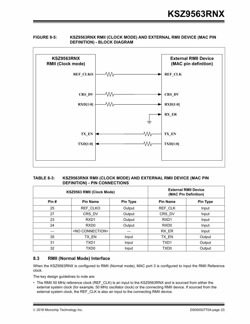
8.3 RMII (Normal Mode) Interface
When the KSZ9563RNX is configured to RMII (Normal mode), MAC port 3 is configured to input the RMII Reference clock.
The key design guidelines to note are:
• The RMII 50 MHz reference clock (REF_CLK) is an input to the KSZ9563RNX and is sourced from either the external system clock (for example, 50 MHz oscillator clock) or the connecting RMII device. If sourced from the external system clock, the REF_CLK is also an input to the connecting RMII device.
2018 Microchip Technology Inc. DS00002770A-page 23

KSZ9563RNX
• The receive error (RX_ER) signal is not supported by the KSZ9563RNX. The external RMII MAC with the RX_ER input should have this pin pulled low or tied to ground, and the external RMII PHY with the RX_ER output should have this pin left as a no connect.
• Users need to ensure the RMII timing is met between two connecting RMII devices. RMII timing uses a common 50 MHz reference clock between two connecting RMII devices. The RMII timing margin becomes critical when the REF_CLK source is located within or is placed close to one RMII device, with the other RMII device placed further away or across the backplane connector.
Note: The 50 MHz RMII clock has a 20 ns clock period. With minimum specification requirements of 4 ns and 2 ns for the input setup and hold times, the RMII clock period is left with 14 ns (20 ns minus 6 ns for setup/hold times) to cover the transmit output delay and round trip PCB trace delays for the RMII device located furtherest away from the REF_CLK. For example, if the farthest RMII device has the worst case transmit output delay of 12 ns, the PCB trace delay between the two connecting RMII devices is limited to 2 ns (round trip) or 1 ns (one-way).
• It is recommended to place series termination resistors on all RMII output pins. Refer to Figure 8-6 for output pin placement. Combined with the output pin impedance, these series resistors provide the means to tune and match the PCB trace impedance to minimize ringing, and thus improve signal integrity and reduce EMI. The typical resis-tor value ranges from 22Ω to 50Ω with the optimum value being dependent on the board layout. A resistor value of 33Ω can be used as the starting point for the schematic design.
The KSZ9563RNX RMII (Normal mode) signal connections with an external RMII device (PHY pin definition) are shown in Figure 8-6 and Table 8-4.
FIGURE 8-6: KSZ9563RNX RMII (NORMAL MODE) AND EXTERNAL RMII DEVICE (PHY PIN DEFINITION) - BLOCK DIAGRAM
KSZ9563RNXRMII (Normal Mode)
TXD[1:0]
RXD[1:0]
CRS_DV
External RMII Device(PHY pin definition)
TX_EN
RXD[1:0]
CRS_DV
TXD[1:0]
TX_EN
REF_CLKI REF_CLK
RX_ER
(Output clock as shown, or Input clock if supported)
Note: Always check the pin types in the data sheet for the connecting RMII pins between two devices to ensure the adjoining pins are neither both inputs nor both outputs. Do not rely on just the pin name of the RMII interface between two connecting devices. The same pin name may be defined as an input or an output depending on the interface perspective.
DS00002770A-page 24 2018 Microchip Technology Inc.

KSZ9563RNX
TABLE 8-4: KSZ9563RNX RMII (NORMAL MODE) AND EXTERNAL RMII DEVICE (PHY PIN DEFINITION) - PIN CONNECTIONS
KSZ9563RNX RMII (Normal Mode)External RMII Device(PHY Pin Definition)
Pin # Pin Name Pin Type Pin Name Pin Type
33 REFCLKI Input REF_CLK Output/Input
27 CRS_DV Output TX_EN Input
23 RXD1 Output TXD1 Input
24 RXD0 Output TXD0 Input
35 TX_EN Input CRS_DV Output
31 TXD1 Input RXD1 Output
32 TXD0 Input RXD0 Output
— <NO CONNECTION> — RX_ER Output
8.4 MII (MAC Mode) Interface
When the KSZ9563RNX is configured to MII (MAC mode), MAC port 3 is configured like an MII MAC device. The key design guidelines to note are:
• Transmit clock (TX_CLK) and receive clock (RX_CLK) are inputs to the KSZ9563RNX and outputs from the exter-nal MII PHY.
• Collision (COL) and carrier sense (CRS) inputs are not supported by the KSZ9563RNX. The external MII PHY with COL and CRS outputs should have these two pins left as no connects.
• It is recommended to place series termination resistors on all MII output pins. Refer to Figure 8-8 for output pin placement. Combined with the output pin impedance, these series resistors provide the means to tune and match the PCB trace impedance to minimize ringing, and thus improve signal integrity and reduce EMI. The typical resis-tor value ranges from 22Ω to 50Ω with the optimum value being dependent on the board layout. A resistor value of 33Ω can be used as the starting point for the schematic design.
The KSZ9563RNX MII (MAC mode) signal connections with an external MII PHY are shown in Figure 8-7 and Table 8-5.
Note: Always check the pin types in the data sheet for the connecting MII pins between two devices to ensure the adjoining pins are not both inputs and not both outputs. Do not rely on just the pin name of the MII inter-face between two connecting devices. The same pin name may be defined as an input or an output depending on the interface perspective.
2018 Microchip Technology Inc. DS00002770A-page 25

KSZ9563RNX
FIGURE 8-7: KSZ9563RNX MII (MAC MODE) AND EXTERNAL MII PHY - BLOCK DIAGRAM
KSZ9563RNXMII (MAC Mode)
TXD[3:0]
RXD[3:0]
RX_CLK
RX_DV
External MII PHY Device
TX_CLK
TX_EN
RXD[3:0]
RX_CLK
RX_DV
TXD[3:0]
TX_CLK
TX_EN
RX_ER TX_ER
TX_ER RX_ER
CRS
COL
TABLE 8-5: KSZ9563RNX MII (MAC MODE) AND EXTERNAL MII PHY - PIN CONNECTIONS
KSZ9563RNX MII (MAC Mode) External MII PHY Device
Pin # Pin Name Pin Type Pin Name Pin Type
33 TX_CLK Input RX_CLK Output
35 TX_EN Input RX_DV Output
29 TXD3 Input RXD3 Output
30 TXD2 Input RXD2 Output
31 TXD1 Input RXD1 Output
32 TXD0 Input RXD0 Output
36 TX_ER Input RX_ER Output
25 RX_CLK Input TX_CLK Output
27 RX_DV Output TX_EN Input
21 RXD3 Output TXD3 Input
22 RXD2 Output TXD2 Input
23 RXD1 Output TXD1 Input
24 RXD0 Output TXD0 Input
28 RX_ER Output TX_ER Input
— <NO CONNECTION> — CRS Output
— <NO CONNECTION> — COL Output
DS00002770A-page 26 2018 Microchip Technology Inc.

KSZ9563RNX
8.5 MII (PHY Mode) Interface
When the KSZ9563RNX is configured to MII (PHY mode), MAC port 3 is configured like an MII PHY device. The key design guidelines to note are:
• Transmit clock (TX_CLK) and receive clock (RX_CLK) are outputs from the KSZ9563RNX and inputs into the external MII MAC.
• Collision (COL) and carrier sense (CRS) outputs are not supported by the KSZ9563RNX. External MII MAC with COL and CRS inputs should have these two pins pulled low or tied to ground.
• It is recommended to place series termination resistors on all MII output pins. Refer to Figure 8-8 for output pin placement. Combined with the output pin impedance, these series resistors provide the means to tune and match the PCB trace impedance to minimize ringing, and thus improve signal integrity and reduce EMI. The typical resis-tor value ranges from 22Ω to 50Ω with the optimum value being dependent on the board layout. A resistor value of 33Ω can be used as the starting point for the schematic design.
The KSZ9563RNX MII (PHY mode) signal connections with an external MII MAC are shown in Figure 8-8 and Table 8-6.
FIGURE 8-8: KSZ9563RNX MII (PHY MODE) AND EXTERNAL MII MAC - BLOCK DIAGRAM
KSZ9563RNXMII (PHY Mode)
TXD[3:0]
RXD[3:0]
RX_CLK
RX_DV
External MII MAC Device
TX_CLK
TX_EN
TXD[3:0]
TX_CLK
TX_EN
RXD[3:0]
RX_CLK
RX_DV
RX_ER RX_ER
TX_ER TX_ER
CRS
COL
Note: Always check the pin types in the data sheet for the connecting MII pins between two devices to ensure the adjoining pins are not both inputs and not both outputs. Do not rely on just the pin name of the MII inter-face between two connecting devices. The same pin name may be defined as an input or an output depending on the interface perspective.
2018 Microchip Technology Inc. DS00002770A-page 27

KSZ9563RNX
TABLE 8-6: KSZ9563RNX MII (PHY MODE) AND EXTERNAL MII MAC - PIN CONNECTIONS
KSZ9563RNX MII (PHY Mode) External MII MAC Device
Pin # Pin Name Pin Type Pin Name Pin Type
33 TX_CLK Output TX_CLK Input
35 TX_EN Input TX_EN Output
29 TXD3 Input TXD3 Output
30 TXD2 Input TXD2 Output
31 TXD1 Input TXD1 Output
32 TXD0 Input TXD0 Output
36 TX_ER Input TX_ER Output
25 RX_CLK Output RX_CLK Input
27 RX_DV Output RX_DV Input
21 RXD3 Output RXD3 Input
22 RXD2 Output RXD2 Input
23 RXD1 Output RXD1 Input
24 RXD0 Output RXD0 Input
28 RX_ER Output RX_ER Input
— <NO CONNECTION> — CRS Output
— <NO CONNECTION> — COL Output
DS00002770A-page 28 2018 Microchip Technology Inc.

KSZ9563RNX
9.0 LED INDICATOR PINS
The LEDx_x pins are inputs and function as the multiplexed strapping pins (see Section 2.3, "Configuration Strap Pins") during chip power-up or hardware pin reset when the RESET_N input (pin 46) is asserted (driven low).
The LEDx_x pins are totem pole outputs to drive LED indicators to indicate the PHY ports’ speed, link, and activity status when the RESET_N input is not asserted (driven high).
9.1 PHY Port LED Status and Pin Strapping - for VDDIO = 3.3V or 2.5V
Figure 9-1 shows the pull-up, float, and pull-down reference circuits for the multiplexed PHY port LED status and pin strapping for 3.3V and 2.5V VDDIO.
FIGURE 9-1: PHY Port LED Status and Pin Strapping - for VDDIO = 3.3V or 2.5V
LEDx_x pin
VDDIO = 3.3V, 2.5V
Pull-up
KSZ9563RNX
Float
KSZ9563RNX
LEDx_x pin
Pull-down
KSZ9563RNX
LEDx_x pin
VDDIO = 3.3V, 2.5V
VDDIO = 3.3V, 2.5V
VDDIO = 3.3V, 2.5V
VDDIO = 3.3V, 2.5V
VDDIO = 3.3V, 2.5V
2018 Microchip Technology Inc. DS00002770A-page 29

KSZ9563RNX
9.2 PHY Port LED Status and Pin Strapping - for VDDIO = 1.8V
Figure 9-2 shows the pull-up, float, and pull-down reference circuits for the multiplexed PHY port LED status and pin strapping for 1.8V VDDIO. The open-drain buffers serve as level shifters and are needed to turn on the LED indicators that require voltage drops of 1.6V to 2.2V, depending on the LED color.
FIGURE 9-2: PHY Port LED Status and Pin Strapping - for VDDIO = 1.8V
3.3V, 2.5V
3.3V, 2.5V
3.3V, 2.5V
LEDx_x pin
Pull-up
KSZ9563RNX
Float
KSZ9563RNX
LEDx_x pin
Pull-down
KSZ9563RNX
LEDx_x pin
VDDIO = 1.8V
VDDIO = 1.8V
VDDIO = 1.8V
Buffer (open-drain)
VDDIO = 1.8V
Buffer (open-drain)
VDDIO = 1.8V
Buffer (open-drain)
VDDIO = 1.8V
DS00002770A-page 30 2018 Microchip Technology Inc.

KSZ9563RNX
10.0 GPIO PINS
The GPIO_1 and GPIO_2 pins are designed to support IEEE 1588 Precision Time Protocol (PTP) applications, and are configurable to implement event trigger outputs and timestamp capture inputs to support real-time application require-ments.
The GPIO_1 and GPIO_2 pins do not support general purpose input or output usage.
11.0 MISCELLANEOUS
11.1 INTRP_N Output
The INTRP_N (pin 45) is the interrupt output. It is active low and requires an external 1.0-4.7 kΩ pull-up resistor to the KSZ9563 VDDIO power rail.
Refer to KSZ9563 Data Sheet for configurable interrupt events.
11.2 PME_N Output
The PME_N (pin 44) output provides the Power Management Event (PME) interrupt output for the Wake-on-LAN (WoL) function. When the PME_N pin is asserted, it indicates that the KSZ9563 device has detected an energy event and is outputting the interrupt to wake up the system from a low power mode.
The PME_N asserted polarity is programmable (default is active low). An external pull-up resistor is required for active-low operation. An external pull-down resistor is required for active-high operation. For both cases, the external resistor value is 1.0-4.7 kΩ.
Refer to KSZ9563 Data Sheet for further details and usage on the PME_N signal and WoL function.
11.3 EMI Consideration
Incorporate a large SMD footprint (SMD_1210) to connect the chassis ground to the digital ground. This allows some flexibility at EMI testing for different grounding options. Leaving the footprint open will allow the two grounds to remain separate. Shorting them together with a zero ohm resistor will connect them. For best performance, short them together with a cap or a ferrite bead.
12.0 REFERENCE MATERIALS
Check Microchip website (www.microchip.com) for the latest version of the following KSZ9563RNX collaterals:
• KSZ9563R Data Sheet
• KSZ9563R Silicon Errata and Data Sheet Clarification
• KSZ9563R IBIS Model
• EVB-KSZ9563 Board Schematic and PCB Layout
• EVB-KSZ9563 Evaluation Board User’s Guide
2018 Microchip Technology Inc. DS00002770A-page 31
KS
Z9563R
NX
DS
00002770A
-page 32
2018 M
icrochip Technolo
gy Inc.
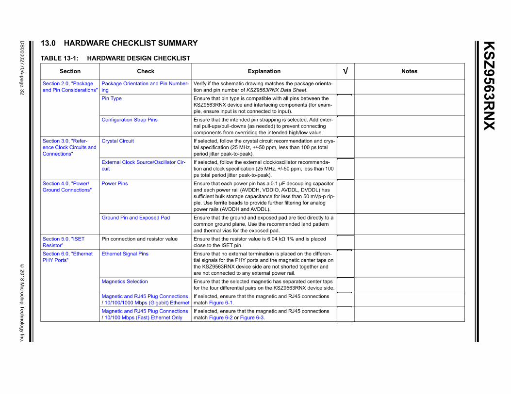
13.0 HARDWARE CHECKLIST SUMMARY
TABLE 13-1: HARDWARE DESIGN CHECKLIST
Section Check Explanation √ Notes
Section 2.0, "Package and Pin Considerations"
Package Orientation and Pin Number-ing
Verify if the schematic drawing matches the package orienta-tion and pin number of KSZ9563RNX Data Sheet.
Pin Type Ensure that pin type is compatible with all pins between the KSZ9563RNX device and interfacing components (for exam-ple, ensure input is not connected to input).
Configuration Strap Pins Ensure that the intended pin strapping is selected. Add exter-nal pull-ups/pull-downs (as needed) to prevent connecting components from overriding the intended high/low value.
Section 3.0, "Refer-ence Clock Circuits and Connections"
Crystal Circuit If selected, follow the crystal circuit recommendation and crys-tal specification (25 MHz, +/-50 ppm, less than 100 ps total period jitter peak-to-peak).
External Clock Source/Oscillator Cir-cuit
If selected, follow the external clock/oscillator recommenda-tion and clock specification (25 MHz, +/-50 ppm, less than 100 ps total period jitter peak-to-peak).
Section 4.0, "Power/Ground Connections"
Power Pins Ensure that each power pin has a 0.1 µF decoupling capacitor and each power rail (AVDDH, VDDIO, AVDDL, DVDDL) has sufficient bulk storage capacitance for less than 50 mVp-p rip-ple. Use ferrite beads to provide further filtering for analog power rails (AVDDH and AVDDL).
Ground Pin and Exposed Pad Ensure that the ground and exposed pad are tied directly to a common ground plane. Use the recommended land pattern and thermal vias for the exposed pad.
Section 5.0, "ISET Resistor"
Pin connection and resistor value Ensure that the resistor value is 6.04 kΩ 1% and is placed close to the ISET pin.
Section 6.0, "Ethernet PHY Ports"
Ethernet Signal Pins Ensure that no external termination is placed on the differen-tial signals for the PHY ports and the magnetic center taps on the KSZ9563RNX device side are not shorted together and are not connected to any external power rail.
Magnetics Selection Ensure that the selected magnetic has separated center taps for the four differential pairs on the KSZ9563RNX device side.
Magnetic and RJ45 Plug Connections / 10/100/1000 Mbps (Gigabit) Ethernet
If selected, ensure that the magnetic and RJ45 connections match Figure 6-1.
Magnetic and RJ45 Plug Connections / 10/100 Mbps (Fast) Ethernet Only
If selected, ensure that the magnetic and RJ45 connections match Figure 6-2 or Figure 6-3.
2018
Microchip T
echnology Inc.D
S0
0002770A-p
age 33
KS
Z9563R
NX
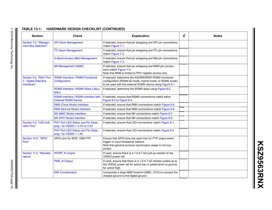
Section 7.0, "Manage-ment Bus Selection"
SPI Slave Management If selected, ensure that pin strapping and SPI pin connections match Figure 7-1.
I2C Slave Management If selected, ensure that pin strapping and I2C pin connections match Figure 7-2.
In-Band Access (IBA) Management If selected, ensure that pin strapping and IBA pin connections match Figure 7-3.
MII Management (MIIM) If selected, ensure that pin strapping and MIIM pin connec-tions match Figure 7-4.Note that MIIM is limited to PHY register access only.
Section 8.0, "MAC Port 3 - Digital Data Bus Interfaces"
RGMII Interface / RGMII Functional Configuration
If selected, determine the KSZ9563RNX RGMII functional configuration (RGMII-ID mode, Hybrid mode, or RGMII mode) to be used with the external RGMII device using Figure 8-1.
RGMII Interface / RGMII Skew Calcu-lation
If selected, determine the RGMII skew using Figure 8-2.
RGMII Interface / RGMII Interface with External RGMII Device
If selected, ensure that RGMII connections match either Figure 8-3 or Figure 8-4.
RMII (Clock Mode) Interface If selected, ensure that RMII connections match Figure 8-5.
RMII (Normal Mode) Interface If selected, ensure that RMII connections match Figure 8-6.
MII (MAC Mode) Interface If selected, ensure that MII connections match Figure 8-7.
MII (PHY Mode) Interface If selected, ensure that MII connections match Figure 8-8.
Section 9.0, "LED Indi-cator Pins"
PHY Port LED Status and Pin Strap-ping - for VDDIO = 3.3V or 2.5V
If selected, ensure that LED connections match Figure 9-1.
PHY Port LED Status and Pin Strap-ping - for VDDIO = 1.8V
If selected, ensure that LED connections match Figure 9-2.
Section 10.0, "GPIO Pins"
GPIO pins for IEEE 1588 PTP Ensure that GPIO pins are used only for PTP output event trigger or input timestamp capture.Note that general purpose input/output usage is not sup-ported.
Section 11.0, "Miscella-neous"
INTRP_N Output If used, ensure there is a 1.0-4.7 kΩ pull-up resistor to the VDDIO power rail.
PME_N Output If used, ensure that there is a 1.0-4.7 kΩ resistor pulled-up to the VDDIO power rail for active low or pulled-down to ground for active high.
EMI Consideration Incorporate a large SMD footprint (SMD_1210) to connect the chassis ground to the digital ground.
TABLE 13-1: HARDWARE DESIGN CHECKLIST (CONTINUED)
Section Check Explanation √ Notes

KSZ9563RNX
APPENDIX A: REVISION HISTORY
TABLE A-1: REVISION HISTORY
Revision Level & Date Section/Figure/Entry Correction
DS00002770A (08-20-18)
Initial release.
DS00002770A-page 34 2018 Microchip Technology Inc.

KSZ9563RNX
THE MICROCHIP WEBSITE
Microchip provides online support via our WWW site at www.microchip.com. This website is used as a means to make files and information easily available to customers. Accessible by using your favorite Internet browser, the website contains the following information:
• Product Support – Data sheets and errata, application notes and sample programs, design resources, user’s guides and hardware support documents, latest software releases and archived software
• General Technical Support – Frequently Asked Questions (FAQ), technical support requests, online discussion groups, Microchip consultant program member listing
• Business of Microchip – Product selector and ordering guides, latest Microchip press releases, listing of seminars and events, and listings of Microchip sales offices, distributors and factory representatives
CUSTOMER CHANGE NOTIFICATION SERVICE
Microchip’s customer notification service helps keep customers current on Microchip products. Subscribers will receive e-mail notification whenever there are changes, updates, revisions, or errata related to a specified product family or development tool of interest.
To register, access the Microchip website at www.microchip.com. Under “Support”, click on “Customer Change Notifi-cation” and follow the registration instructions.
CUSTOMER SUPPORT
Users of Microchip products can receive assistance through several channels:
• Distributor or Representative
• Local Sales Office
• Field Application Engineer (FAE)
• Technical Support
Customers should contact their distributor, representative or Field Application Engineer (FAE) for support. Local sales offices are also available to help customers. A listing of sales offices and locations is included in the back of this document.
Technical support is available through the website at: http://microchip.com/support.
2018 Microchip Technology Inc. DS00002770A-page 35

KSZ9563RNX
NOTES:
DS00002770A-page 36 2018 Microchip Technology Inc.

2018 Microchip Technology Inc. DS00002770A-page 37
Note the following details of the code protection feature on Microchip devices:
• Microchip products meet the specification contained in their particular Microchip Data Sheet.
• Microchip believes that its family of products is one of the most secure families of its kind on the market today, when used in the intended manner and under normal conditions.
• There are dishonest and possibly illegal methods used to breach the code protection feature. All of these methods, to our knowledge, require using the Microchip products in a manner outside the operating specifications contained in Microchip’s Data Sheets. Most likely, the person doing so is engaged in theft of intellectual property.
• Microchip is willing to work with the customer who is concerned about the integrity of their code.
• Neither Microchip nor any other semiconductor manufacturer can guarantee the security of their code. Code protection does not mean that we are guaranteeing the product as “unbreakable.”
Code protection is constantly evolving. We at Microchip are committed to continuously improving the code protection features of our products. Attempts to break Microchip’s code protection feature may be a violation of the Digital Millennium Copyright Act. If such acts allow unauthorized access to your software or other copyrighted work, you may have a right to sue for relief under that Act.
Microchip received ISO/TS-16949:2009 certification for its worldwide headquarters, design and wafer fabrication facilities in Chandler and Tempe, Arizona; Gresham, Oregon and design centers in California and India. The Company’s quality system processes and procedures are for its PIC® MCUs and dsPIC® DSCs, KEELOQ® code hopping devices, Serial EEPROMs, microperipherals, nonvolatile memory and analog products. In addition, Microchip’s quality system for the design and manufacture of development systems is ISO 9001:2000 certified.
QUALITYMANAGEMENTSYSTEMCERTIFIEDBYDNV
== ISO/TS16949==
Information contained in this publication regarding device applications and the like is provided only for your convenience and may be superseded by updates. It is your responsibility to ensure that your application meets with your specifications. MICROCHIP MAKES NO REPRESENTATIONS OR WARRANTIES OF ANY KIND WHETHER EXPRESS OR IMPLIED, WRITTEN OR ORAL, STATUTORY OR OTHERWISE, RELATED TO THE INFORMATION, INCLUDING BUT NOT LIMITED TO ITS CONDITION, QUALITY, PERFORMANCE, MERCHANTABILITY OR FITNESS FOR PURPOSE. Microchip disclaims all liability arising from this information and its use. Use of Micro-chip devices in life support and/or safety applications is entirely at the buyer’s risk, and the buyer agrees to defend, indemnify and hold harmless Microchip from any and all damages, claims, suits, or expenses resulting from such use. No licenses are conveyed, implicitly or otherwise, under any Microchip intellectual property rights unless otherwise stated.
Trademarks
The Microchip name and logo, the Microchip logo, AnyRate, AVR, AVR logo, AVR Freaks, BitCloud, chipKIT, chipKIT logo, CryptoMemory, CryptoRF, dsPIC, FlashFlex, flexPWR, Heldo, JukeBlox, KeeLoq, Kleer, LANCheck, LINK MD, maXStylus, maXTouch, MediaLB, megaAVR, MOST, MOST logo, MPLAB, OptoLyzer, PIC, picoPower, PICSTART, PIC32 logo, Prochip Designer, QTouch, SAM-BA, SpyNIC, SST, SST Logo, SuperFlash, tinyAVR, UNI/O, and XMEGA are registered trademarks of Microchip Technology Incorporated in the U.S.A. and other countries.
ClockWorks, The Embedded Control Solutions Company, EtherSynch, Hyper Speed Control, HyperLight Load, IntelliMOS, mTouch, Precision Edge, and Quiet-Wire are registered trademarks of Microchip Technology Incorporated in the U.S.A.
Adjacent Key Suppression, AKS, Analog-for-the-Digital Age, Any Capacitor, AnyIn, AnyOut, BodyCom, CodeGuard, CryptoAuthentication, CryptoAutomotive, CryptoCompanion, CryptoController, dsPICDEM, dsPICDEM.net, Dynamic Average Matching, DAM, ECAN, EtherGREEN, In-Circuit Serial Programming, ICSP, INICnet, Inter-Chip Connectivity, JitterBlocker, KleerNet, KleerNet logo, memBrain, Mindi, MiWi, motorBench, MPASM, MPF, MPLAB Certified logo, MPLIB, MPLINK, MultiTRAK, NetDetach, Omniscient Code Generation, PICDEM, PICDEM.net, PICkit, PICtail, PowerSmart, PureSilicon, QMatrix, REAL ICE, Ripple Blocker, SAM-ICE, Serial Quad I/O, SMART-I.S., SQI, SuperSwitcher, SuperSwitcher II, Total Endurance, TSHARC, USBCheck, VariSense, ViewSpan, WiperLock, Wireless DNA, and ZENA are trademarks of Microchip Technology Incorporated in the U.S.A. and other countries.
SQTP is a service mark of Microchip Technology Incorporated in the U.S.A.
Silicon Storage Technology is a registered trademark of Microchip Technology Inc. in other countries.
GestIC is a registered trademark of Microchip Technology Germany II GmbH & Co. KG, a subsidiary of Microchip Technology Inc., in other countries.
All other trademarks mentioned herein are property of their respective companies.
© 2018, Microchip Technology Incorporated, All Rights Reserved.
ISBN: 978-1-5224-3443-6

DS00002770A-page 38 2018 Microchip Technology Inc.
AMERICASCorporate Office2355 West Chandler Blvd.Chandler, AZ 85224-6199Tel: 480-792-7200 Fax: 480-792-7277Technical Support: http://www.microchip.com/supportWeb Address: www.microchip.com
AtlantaDuluth, GA Tel: 678-957-9614 Fax: 678-957-1455
Austin, TXTel: 512-257-3370
BostonWestborough, MA Tel: 774-760-0087 Fax: 774-760-0088
ChicagoItasca, IL Tel: 630-285-0071 Fax: 630-285-0075
DallasAddison, TX Tel: 972-818-7423 Fax: 972-818-2924
DetroitNovi, MI Tel: 248-848-4000
Houston, TX Tel: 281-894-5983
IndianapolisNoblesville, IN Tel: 317-773-8323Fax: 317-773-5453Tel: 317-536-2380
Los AngelesMission Viejo, CA Tel: 949-462-9523Fax: 949-462-9608Tel: 951-273-7800
Raleigh, NC Tel: 919-844-7510
New York, NY Tel: 631-435-6000
San Jose, CA Tel: 408-735-9110Tel: 408-436-4270
Canada - TorontoTel: 905-695-1980 Fax: 905-695-2078
ASIA/PACIFICAustralia - SydneyTel: 61-2-9868-6733
China - BeijingTel: 86-10-8569-7000
China - ChengduTel: 86-28-8665-5511
China - ChongqingTel: 86-23-8980-9588
China - DongguanTel: 86-769-8702-9880
China - GuangzhouTel: 86-20-8755-8029
China - HangzhouTel: 86-571-8792-8115
China - Hong Kong SARTel: 852-2943-5100
China - NanjingTel: 86-25-8473-2460
China - QingdaoTel: 86-532-8502-7355
China - ShanghaiTel: 86-21-3326-8000
China - ShenyangTel: 86-24-2334-2829
China - ShenzhenTel: 86-755-8864-2200
China - SuzhouTel: 86-186-6233-1526
China - WuhanTel: 86-27-5980-5300
China - XianTel: 86-29-8833-7252
China - XiamenTel: 86-592-2388138
China - ZhuhaiTel: 86-756-3210040
ASIA/PACIFICIndia - BangaloreTel: 91-80-3090-4444
India - New DelhiTel: 91-11-4160-8631
India - PuneTel: 91-20-4121-0141
Japan - OsakaTel: 81-6-6152-7160
Japan - TokyoTel: 81-3-6880- 3770
Korea - DaeguTel: 82-53-744-4301
Korea - SeoulTel: 82-2-554-7200
Malaysia - Kuala LumpurTel: 60-3-7651-7906
Malaysia - PenangTel: 60-4-227-8870
Philippines - ManilaTel: 63-2-634-9065
SingaporeTel: 65-6334-8870
Taiwan - Hsin ChuTel: 886-3-577-8366
Taiwan - KaohsiungTel: 886-7-213-7830
Taiwan - TaipeiTel: 886-2-2508-8600
Thailand - BangkokTel: 66-2-694-1351
Vietnam - Ho Chi MinhTel: 84-28-5448-2100
EUROPEAustria - WelsTel: 43-7242-2244-39Fax: 43-7242-2244-393
Denmark - CopenhagenTel: 45-4450-2828 Fax: 45-4485-2829
Finland - EspooTel: 358-9-4520-820
France - ParisTel: 33-1-69-53-63-20 Fax: 33-1-69-30-90-79
Germany - GarchingTel: 49-8931-9700
Germany - HaanTel: 49-2129-3766400
Germany - HeilbronnTel: 49-7131-67-3636
Germany - KarlsruheTel: 49-721-625370
Germany - MunichTel: 49-89-627-144-0 Fax: 49-89-627-144-44
Germany - RosenheimTel: 49-8031-354-560
Israel - Ra’anana Tel: 972-9-744-7705
Italy - Milan Tel: 39-0331-742611 Fax: 39-0331-466781
Italy - PadovaTel: 39-049-7625286
Netherlands - DrunenTel: 31-416-690399 Fax: 31-416-690340
Norway - TrondheimTel: 47-7288-4388
Poland - WarsawTel: 48-22-3325737
Romania - BucharestTel: 40-21-407-87-50
Spain - MadridTel: 34-91-708-08-90Fax: 34-91-708-08-91
Sweden - GothenbergTel: 46-31-704-60-40
Sweden - StockholmTel: 46-8-5090-4654
UK - WokinghamTel: 44-118-921-5800Fax: 44-118-921-5820
Worldwide Sales and Service
08/15/18