keysight technologies advanced nanomeasurement solutions
TRANSCRIPT

Keysight TechnologiesAdvanced Nanomeasurement Solutions

Advanced Nanomeasurement Solutionsfor Research, Industry & Education
Keysight Technologies meets your unique nanomeasurement requirements with a variety of flexible scientific-grade solutions
Whether your application requires a high-resolution system that offers modularity and cross-platform compatibility for atomic force microscopy (AFM) and scanning probe microscopy (SPM), a nanoindenter or universal testing machine (UTM) optimized for high-precision nanomechanical characterization, or a compact, low-voltage system that delivers exceptional field emission scanning electron microscopy (FE-SEM) performance, Keysight Technologies, Inc. is committed to providing the right state-of-the-art instrumentation for your work.
When you choose Keysight, you’re choosing a reliable partner with a long history of nanomeasurement innovation. Keysight was the first to offer SPM for imaging in fluids and controlled environments, a technological legacy that continues to manifest itself in a wide range of superior solutions for in-fluid and soft-sample imaging. We hold more than 40 AFM-related patents and our leading-edge R&D is committed to the pursuit of advancements that will make atomic force microscopy easier to use. More than 2,500 peer-reviewed papers have been published using Keysight AFM technology, further validating its high performance and versatility.
The pedigree of our nanomechanical test instrumentation is equally impressive. For instance, the seminal paper authored by Warren Oliver and George Pharr has now surpassed 5,000 citations, making it the most frequently cited paper for nanomechanical properties of materials.
Every Keysight nanomeasurement solution is backed by a team of knowledgeable application scientists and technical service personnel, all of whom strive to provide outstanding support to our customers around the world. We offer invaluable application expertise for life science, materials science, polymer science, electrochemistry, and cross-disciplinary nanoscale research.
Our driving goal is to help you be the first to see, the first to understand, and the first to publish!

03 | Keysight | Advanced Nanomeasurement Solutions - Brochure
The Keysight Atomic Force Microscope Solutions
10 sec/frame scanning of a polydiethylsiloxane (PDES) on silicon. Left image at 25 °C, right at 46 °C.
Keysight 9500 AFM Series
The 9500 AFM seamlessly integrates revolutionary new software, a new high-bandwidth digital controller, and a state-of-the-art mechanical design to provide unrivaled scan rates at 2 sec. per frame and truly astonishing ease of use. In addition to completely redefining the user experience for atomic force microscopes, this intelligently conceived system delivers the superior performance and flexible functionality that scientists and engineers have come to expect from Keysight Technologies.
Advantages – New NanoNavigator software with
workflow-based GUI – Quick Scan for ultrafast scanning
(100 lines/sec, 2 sec/frame) – Auto Drive automatically sets all
parameters within seconds – Mobile app allows remote monitoring
of system operation – New high-bandwidth digital controller
ensures high-speed precision – 90 µm closed-loop scanner delivers
atomic resolution
Applications – Materials science – Life science – Polymer science – Electrical characterization
KFM SP channel image (left), conducting polymer on AU substrate (center), 3D CSAFM WTi image (right).
Keysight 7500 AFM Series
The Keysight 7500 AFM establishes new functionality, versatility, and ease-of-use benchmarks for nanoscale measurement, charac-terization, and manipulation. This next-generation system extends the forefront of atomic force microscopy, offering 90 µm closed-loop scanning atomic resolution, industry-leading environmental control, ultra-high- precision temperature control, an unrivaled range of electrochemistry capabilities, and much more. The clever, compact design of the 7500 gives researchers quick, convenient access to their samples. A half-dozen distinct AFM imaging modes are supported by the system’s standard nose cone, which can easily be interchanged with specialized nose cones as needed, extending capability effortlessly.
Advantages – Atomic scale imaging with
closed loop 90 μm scanner – Exceptional environmental and
temperature control – Superior scanning in fluids, gases,
and ambient conditions – Single-pass nanoscale electrical
characterization – Unprecedented electrochemistry
(EC) capabilities – Standard nose cone supports
expanded set of imaging modes
Applications – Life science – Materials science – Polymer science – Electrochemistry – Nanolithography
04 | Keysight | Advanced Nanomeasurement Solutions - Brochure
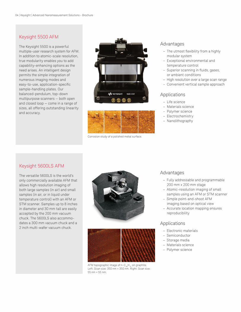
AFM topographic image of n-C36H74 on graphite. Left: Scan size: 350 nm × 350 nm. Right: Scan size: 55 nm × 55 nm.
Advantages – Fully addressable and programmable
200 mm x 200 mm stage – Atomic-resolution imaging of small
samples using an AFM or STM scanner – Simple point-and-shoot AFM
imaging based on optical view – Accurate location mapping ensures
reproducibility
Applications – Electronic materials – Semiconductor – Storage media – Materials science – Polymer science
Keysight 5600LS AFM
The versatile 5600LS is the world’s only commercially available AFM that allows high resolution imaging of both large samples (in air) and small samples (in air, or in liquid under temperature control) with an AFM or STM scanner. Samples up to 8 inches in diameter and 30 mm tall are easily accepted by the 200 mm vacuum chuck. The 5600LS also accommo-dates a 300 mm vacuum chuck and a 2 inch multi-wafer vacuum chuck.
Corrosion study of a polished metal surface.
Keysight 5500 AFM
The Keysight 5500 is a powerful multiple-user research system for AFM. In addition to atomic-scale resolution, true modularity enables you to add capability-enhancing options as the need arises. An intelligent design permits the simple integration of numerous imaging modes and easy-to-use, application-specific sample-handling plates. Our balanced-pendulum, top-down multipurpose scanners — both open and closed loop — come in a range of sizes, all offering outstanding linearity and accuracy.
Advantages – The utmost flexibility from a highly
modular system – Exceptional environmental and
temperature control – Superior scanning in fluids, gases,
or ambient conditions – High resolution over a large scan range – Convenient vertical sample approach
Applications – Life science – Materials science – Polymer science – Electrochemistry – Nanolithography

05 | Keysight | Advanced Nanomeasurement Solutions - Brochure
MAC Mode images of DNA. Scan size 2 µm (left) and protein ferritin, scan size 0.1 µm (right).
Keysight 7500ILM AFM
The Keysight 7500 inverted light microscope (ILM) system combines the power of a high-resolution atomic force microscope (AFM) with the direct optical viewing capability of an inverted optical microscope.
The Keysight ILM offers unparalleled performance and ease of use for imaging in fluids and extends AFM utility. Atomic force and optical (or fluorescence) microscopy data can be obtained simultaneously with the Keysight ILM. The ILM’s patented mounting design incorporates a rigid structure that provides the low noise floor needed to obtain sub-nanometer resolution. Keysight’s QuickSlide sam-ple-loading mechanism and a flexible sample-handling plate make sample preparation easy. The AFM is mounted on the QuickSlide assembly, allowing the user to change samples and/or solutions without affecting the alignment of the AFM or the optical microscope.
Advantages – Top down, tip scanning design enables
intuitive, effortless setup and imaging – Inverted optical view, open-top
viewing access, and top illumination provide superior optical contrast
– Patented MAC Mode option provides gentlest, nondestructive AFM imaging of delicate samples in fluid
– Sample-handling plates available to facilitate easy imaging in fluids or ambient air
– PicoTREC option delivers real-time, simultaneous topography and molecular recognition imaging
Applications – DNA – Cell biology – Proteins – Polymers – Thin films
Left: E-coli bacteria. Right: MAC Mode image of a living endothelial cell in water.
Keysight 5500ILM AFM
The ILM adapter combines high-resolution AFM imaging with the direct optical viewing capability of an inverted light microscope to provide both atomic force and optical microscopy data. Designed to allow the 5500 AFM to sit on top of an inverted microscope and under the top illumination pillar, the Keysight 5500ILM delivers excellent optical contrast in its images. It also enables a wide range of complemen-tary techniques, such as fluorescence resonance energy transfer (FRET), darkfield, and brightfield imaging.
Advantages – Simultaneous AFM and optical
(or fluorescence) imaging – Easy imaging in fluids via MAC Mode
and sample plates – Design gives users open access to
sample plates – Enhanced AFM flexibility through
modular options
Applications – Life science – Polymer science – Nanobeads

06 | Keysight | Advanced Nanomeasurement Solutions - Brochure
Extended Your AFM Capabilities with Keysight’s Options for Materials & Life Sciences
Topography (top) and SECM (bottom) images of an Au/Si sample recorded in 1 mM FeMethanol solution/0.1 MKCl with a combined AFM-SECM probe biased at 240 mV vs. Ag/AgCl.
SECM ModeThe AFM combined with SECM Mode is a seamlessly integrated technology package that enables scientists to perform scanning electrochemical microscopy (SECM) on conductive and insulating samples. This new Keysight mode has been designed to provide ultimate performance as well as supreme ease of use.
At the technological core of the SECM mode is the novel EC SmartCart, an easy-to-handle cartridge that combines a nanoelectrode with a pre-mounted AFM tip. EC SmartCart probes come pre-tested and ready-to-scan for AFM-SECM applications.
Advantages – Performs highly localized electrochemistry via a nanoelectrode combined with a
specialized probe – Customized SECM nosecone designed to be used with EC Smart Cart – Hours of setup time eliminated, so data can be collected immediately
Applications – Homogeneous and heterogeneous electron transfer reactions, – Surface modification, – Analysis of thin films – Screening of catalytic material – Corrosion process studies
SMM images of SiGe: capacitance (top), and dC/dV amplitude (bottom).
SMM ModeKeysight Technologies’ unique scanning microwave microscopy (SMM) Mode combines the comprehensive electrical measurement capabilities of a vector network analyzer (VNA) with the outstanding spatial resolution of an AFM. SMM Mode outperforms traditional AFM-based scanning capacitance microscopy techniques, offering far greater application versatility, the ability to acquire quantitative results, and the highest sensitivity and dynamic range in the industry.
Advantages – Provides exceptionally high spatial and electrical resolution – Enables complex impedance (resistance and reactance), calibrated capacitance,
dopant density and topography measurements – Works on all semiconductors: Si, Ge, III-V (e.g., GaAs, InAs, GaN), and II-VI
(e.g., CdTe, ZnSe) – does not require oxide layer
Application – Semiconductors – Polymers – Ceramics – Metals – Organic films

07 | Keysight | Advanced Nanomeasurement Solutions - Brochure
PicoTREC imaging of the micropat-terned avidin molecules. Topograph-ic image (top), and corresponding recognition image (bottom).
PicoTRECPicoTREC is a system that allows researchers to quickly identify molecules that are engaged in binding events and generate a recognition map along with an AFM topography image of the sample. The system enables many advanced AFM spectros-copy applications such as force-distance studies, generates surface adhesion and molecular recognition profiles.
Advantages – Identifies molecules and regions involved in binding events – Screens compounds/molecules by binding interactions – Improves speed and precision of results
ApplicationsInteractions of
– Antibody-antigen – Ligand-receptor – Drug-receptor – DNA-protein – DNA-DNA
CdTe nanowires. Topography image (top), surface potential (bottom). Scan size 2 μm.
MAC III/Auxiliary Signal AccessKeysight’s MAC Mode III is a technique for AFM that has been designed for imaging extremely delicate samples in high resolution. MAC Mode III enables imaging of sub-molecular structures for local mechanical properties and electromagnetic response. For advanced electrical characterization the auxiliary signal access box, enables single-pass, high resolution imaging with AC Mode, Kelvin force microscopy (KFM) or electric force microscopy (EFM), piezo force microscopy and higher harmonic modes of the cantilever — all simultaneously.
Advantages – Allows one-pass multichannel detection for high resolution EFM and KFM – Three configurable lock-in amplifiers afford superb versatility – Multifrequency range, up to 6 MHz, allowing higher harmonic modes – Built-in Q-control further enhances the resonance peak
Applications – Electrical characterization – Polymers – Biology

08 | Keysight | Advanced Nanomeasurement Solutions - Brochure
AFM Options & Accessories
We offer a wide selection of AFM options and accessories, each of which quickly extends the capabilities of your Keysight atomic force microscope
With our modular platform, these components are simple to integrate.
Among the most useful of all of Keysight’s AFM accessories is MAC Mode. This patented option provides industry-leading performance for in-fluid and soft-sample imaging, allowing you to capture sub-molecular structures that cannot be resolved with any other AFM technique. Advanced MAC Mode III provides three lock-in amplifiers and allows single-pass imaging concurrent with KFM/EFM. It also supports the use of higher resonance modes of the AFM cantilever, enabling higher harmonics and the collection of additional information about mechanical properties of the sample surface.
Another important AFM accessory is Keysight’s exclusive scanning microwave micros-copy (SMM) mode, the first and only technique to combine the calibrated, complex electrical measurement capabilities of a performance network analyzer with the high spatial resolution of an atomic force microscope. This mode enables complex impedance (resistance and reactance), calibrated capacitance, calibrated dopant density, and topography measurements.
Additional accessories include our industry-leading environmental isolation chamber (EIC), which lets you control humidity levels, monitor and control oxygen levels, and control the low of reactive gases during experiments; open- and closed-loop multipur-pose scanners, interchangeable nose cones, and PicoTREC molecular imaging.(KFM) or electric force microscopy (EFM), piezo force microscopy, SECM mode and higher harmonic modes of the cantilever — all simultaneously.
Options/Accessories
– STM
– SECM
– MAC Mode
– MAC Mode III
– SMM Mode
– Environmental Control
– Multipurpose Scanners
– Nose Cones
– Sample Plates
– PicoTREC
– Temperature Control
– Pico Image Software
– Break-out Box
– Glove Box
– Acoustic Isolation Chamber
– Liquid Cells
– Vibration Isolation
– Video Microscope
– Consumables

09 | Keysight | Advanced Nanomeasurement Solutions - Brochure
Nanomechanical Test Equipment
Keysight Nano Indenter G200
The Nano Indenter G200 is the most accurate, flexible, user- friendly instrument commercially available for nanomechanical testing. Electromagnetic actuation allows unparalleled dynamic range in force and displacement. The G200 lets researchers measure Young’s modulus and hardness in compliance with the ISO 14577 standard. It also enables measurement of deformation over six orders of magnitude (from nanometers to millimeters). Users are able to quantify the relationship between structure, properties, and performance of their materials quickly and easily with minimal sample preparation. Express Test allows the Nano Indenter G200 to be operated in controlled-force or controlled-dis-placement mode. Testing is simple, just “point-and-shoot”.
Advantages – Award winning Express Test for
ultrafast testing capabilities (up to 100 indents at 100 different surface sites in 100 seconds)
– Accurate, repeatable results compliant with ISO 14577
– Unparalleled dynamic range in force and displacement
– Dynamic properties characterization via continuous measurement of stiffness by indentation depth
Applications – Semiconductor – Thin films – MEM structures – Hard coatings – DLC films – Biomaterials
Keysight Express Test for the G200
A recent recipient of the prestigious R&D 100 Award, Keysight’s Express Test option enables the world’s fastest nanoindentation for mechanical-prop-erties mapping. This technology, which has been designed and optimized for exclusive use with the Nano Indenter G200, delivers high-precision data on a wide variety of materials. The Express Test option is compatible with all DCM II and XP heads and translation stages.
Achieve ultrafast testing capabilities (up to 100 indents at 100 different surface sites in as little as 100 sec-onds). Express Test allows the G200 to be operated in controlled-force or controlled-displacement mode. Perform area calibration and Young’s modulus in minutes.
Advantages – Ultra-Fast indentation – True mechanical-properties maps – Rapidly evaluates Young’s modulus
and hardness with robust statistics – Histograms automatically generated – Negligible thermal drift
Applications – Metals – Glasses – Ceramics – Structural polymers – Thin films – Low-k materials

10 | Keysight | Advanced Nanomeasurement Solutions - Brochure
Keysight NanoSuite and NanoVision Software
NanoSuite software lets users run tests and manage data with unprece-dented ease. Through the elegant and intuitive interface, you can set up and run experiments quickly — changing test parameters as often as desired — with just a few clicks.
NanoVision software allows you to create quantitative high-resolutionimages using a Keysight Nano Indent-er with a high precision closed-loop stage. User can target indentation test sites with nanometer-scale precision, and examine residual impressions in order to quantify material response phenomena.
Advantages – Load cell delivers high sensitivity
over large range of strain – Largest dynamic range and best
resolution – Flexibility and upgradability for
repeatable or new applications – Real-time control and easy test
protocol development
Applications – Dynamic studies of fibers and
biological materials – Tensile and compression studies of
polymers – Yield of compliant fibers and
biological materials
Keysight T150 UTMThe T150 UTM is a state-of-the-art universal testing machine that offers researchers a superior means of nanomechanical characterization by utilizing a nanomechanical actuating transducer head to produce tensile force. The T150 enables researchers to understand dynamic properties of compliant fibers via the largest dynamic range in the industry and the best resolution on the market (five orders of magnitude of storage and loss modulus).
Advantages – Survey scanning of areas up to
500 μm x 500 μm – Custom test development methods – Superior experiment data analysis – Simulation mode for offline sample
setup, sample runs, method writing, and data analysis
– Quantitative, high-resolution topographical images
– Quantification of pile-up, deformed volume, and fracture toughness

11 | Keysight | Advanced Nanomeasurement Solutions - Brochure
Nanomechanical Options & Accessories
We offer many options and accessories to enhance the capabilities of your Keysight nanoindentation system or universal testing machine
Our modular platform makes these components simple to integrate. We continue to optimize advanced technologies as we strive to push performance even further.
The Keysight Dynamic Contact Module II option, for instance, offers 3x higher loading capability than our original Dynamic Contact Module option. It also offers easy tip exchange for quick removal and installation of application-specific tips, in addition to a wider range of indenter travel. As a fully dynamic indentation head designed for low noise, ultra-low-load mechanical properties characterization, the DCM II extends the range of load-displacement experimentation down to the surface contact level. When applying the Keysight Continuous Stiffness Measurement technique, which provides a means of separating the in-phase and out-of-phase components of the load-displace-ment history, the DCM II delivers the complete benefits of dynamic nanoindentation testing.
Our popular High Load option, on the other hand, expands the load capabilities of Keysight Nano Indenters up to 10N of force, allowing the complete mechanical characterization of ceramics, bulk metals, and composites. Another popular choice, our Lateral Force Measurement option, provides three-dimensional quantitative analysis for scratch testing, wear testing, and MEMs probing. We also offer a precision heating stage designed specifically for the Nano Indenter G200 (standard XP head configuration) to facilitate the study of materials of interest as they are heated from room temperature to as high as 350 ºC.
Keysight T150 UTM users can utilize our Continuous Dynamic Analysis option. This technology offers a direct, accurate measurement of the specimen’s stiffness at each point in the experiment, enabling mechanical properties to be determined continuously as the specimen is strained.
Options/Accessories
– Dynamic Contact
– Module II (DCM II)
– Continuous Stiffness
– Measurement (CSM)
– High Load
– Lateral Force
– Measurement (LFM)
– Continuous Dynamic Analysis (CDA)
– Heating Stage
– Nanovision Software
– Express Test
– Indentation Kit
– Consumables

12 | Keysight | Advanced Nanomeasurement Solutions - Brochure
Keysight FE-SEM for Low-Voltage, High-Performance Imaging
Advantages – Fully integrated EDS capabilities allow quantitative elemental analysis – Resolution and imaging equal to that of conventional FE-SEMs – Variable low voltage (500 to 2000 V) eliminates charging and the need for
sample coating – Programmable X, Y, Z stage allows user to set precise coordinates, scan, and
save information – Compact size enables easy installation in any research lab and does not require
special facilities
Applications – Polymers – Thin films – Biomaterials – Nonconductive samples – Energy-sensitive materials – Glass substrates
Keysight’s NEW 8500B FE-SEMThe remarkably compact Keysight 8500B field-emission scanning electron microscope (FE-SEM) has been optimized for low-voltage imaging, extremely high surface contrast, and resolution typically found only in much larger and more expensive FE-SEMs. This innovative, technologically advanced system also offers fully integrated energy disper-sive spectroscopy (EDS) capabilities, allowing quantitative elemental analysis to be performed on arbitrary points, on a continuous line scan, or in a user-defined regional map. It can detect elements as light as carbon, up to americium.
About the size of a laser printer, this scientific-grade system provides capabilities and performance to researchers in ordinary labs that previously were only available with much larger FE-SEMs installed in centralized facilities. Installation of the new system is quick and simple. No dedicated facilities are required, only an AC power outlet.
The innovative, easy-to-use 8500B embodies the successful miniatur-ization of the core technology found in a scanning electron microscope. Optimized for low-voltage imaging and sub- 10 nm resolution, its thermal field emission electron source provides high signal-to-noise ratios and consistent, long-lasting performance, while secondary and backscatter electron detection capabilities provide a rich data set for each sample.

13 | Keysight | Advanced Nanomeasurement Solutions - Brochure
FE-SEM Options & Accessories
Keysight has created a special SEM startup kit so that when your 8500B FE-SEM is delivered you will have everything you need to start imaging.
The kit includes:
– Specimen mount adapter pin (M4 thread)
– Multi-unit specimen mount (4 x 3.2 mm)
– Package of 100 12 mm Pelco tabs
– Standard SEM pin mounts
– Pelco Swiss style #7 tweezer
– Pelco mount tweezer
– Storage container for SEM mounts
– Specimen holder
– 1/16” ball driver
The following items are also offered for use with the 8500B:
– Specimen mount adapter pin (M4 thread): attaches to the sample holder; used to adjust the working distance of the sample mount
– Standard SEM pin stub mount: 12.7 x 8 mm pin height; aluminum with grooved edge
– Tilt cylinder mount: 9.5 x 9.5 mm, 45° specimen mount (package of 10)
– Cylinder mount: 9.5 x 9.5 mm specimen mount (package of 50)
– Multi specimen cylinder mount holder: holds up to five 9.5mm cylinder mounts; machined aluminum with stainless steel Allen set screws
– Multi 4-pin stub holder: accommodates up to four standard 12.7 mm (1/2”) pin stubs, with 3.2 mm (1/8”) diameter pin; machined aluminum with stainless steel Allen set screws

14 | Keysight | Advanced Nanomeasurement Solutions - Brochure
Materials ScienceIdeal for large and small samples alike, the Keysight 5600LS AFM is a large-stage atomic force microscope compatible with our unique scanning microwave microscopy (SMM) mode, which allows highly sensitive calibrated electrical and spatial characterization. MAC Mode III, which enables Kelvin force microscopy (KFM) and electric force micros-copy (EFM), is available on all Keysight AFMs. The 7500 AFM with temperature and environmental control gives users the advantage of dynamic in-situ imaging. Meanwhile, the new Keysight 8500B FE-SEM with EDS allows nanoscale features to be observed on a wide variety of nanostructured materials, including thin films and other energy-sensi-tive samples, on any substrate.
For nanomechanical testing, Keysight Nano Indenter G200 systems offer accurate and repeatable results compliant with the ISO 14577 standard, along with “low-load first then high-load” capabilities. Additionally, the Keysight T150 UTM enables researchers to understand dynamic properties of compliant fibers and composites via the largest dynamic range and best resolution on the market.
– AFM applications such as electromagnetic measurement – Nanoindenters and low-voltage FE-SEM for measuring DLC thin films, MEM
structures, and nanocomposite fibers
Applications
Life ScienceThe Keysight 7500/5500 series AFM systems facilitate life science investigations by offering a broad array of capabilities, including unrivaled in-fluid imaging (via patented MAC Mode) and industry-leading temperature/environmental control. As new techniques simplify the preparation and handling of diverse sample types, the use of a powerful class of in-situ AFM techniques is becoming increasingly prevalent in biological research. We now offer both the 7500/5500 on an ILM.
In addition, our new 8500B FE-SEM offers several imaging techniques for enhancing surface contrast and allowing nanoscale features to be observed on a broad range of biomaterials on any substrate, even glass.
– Exceptional in-fluid imaging with MAC Mode – Real-time recognition imaging with PicoTREC – Low-voltage FE-SEM imaging of cells, tissue, bacteria, and more

15 | Keysight | Advanced Nanomeasurement Solutions - Brochure
Polymer ScienceKeysight AFMs are used for studying nanoscale composition mapping and materials properties of various polymers under environmental and temperature control. These AFMs adapt to provide phase, friction, and electrical property measurements at atomic-scale resolution over long-range scans utilizing advanced techniques such as MACMode III and high-resolution KFM imaging. What’s more, researchers can now take advantage of the capabilities of our new 8500B FE-SEM with EDS, which has been engineered specifically for low-voltage imaging of nanoscale features on polymers on any substrate.
Polymer studies can also benefit greatly from the use of the Keysight Nano Indenter G200 system. These high-precision nanomechanical test instruments are configurable with our low-noise, ultra-low-load Dynamic Contact Module II (DCM II) option, which provides loading capability up to 30 mN max load.
– AFM and low-voltage FE-SEM for studying surface molecular composition of block copolymers, bulk polymers, thin-film polymers, polymer composites, and polymer blends
– Nanoindenters for ultra-low-load nanomechanical testing of polymers
ElectrochemistryWe offer a highly versatile, easy-to-use option for Keysight 5500 and 7500 AFM users who want to conduct studies involving electrochemistry. A single Keysight electrochem-istry unit has modules that allow in-situ scanning tunneling microscopy (STM), AFM, and conducting-probe capabilities — without compromising atomic resolution. Our unique environmental chamber protects sensitive samples from harsh elements, controls reactive gases, and provides the flexibility required to control a range of parameters during the course of a given experiment. Now available is the new exclusive SECM mode with quick easy set-up.
– Imaging in liquids with patented MAC Mode – Built-in, high-performance potentiostat/galvanostat – State-of-the-art environmental and temperature control
Cross-Disciplinary Nanoscale ResearchIn nanotechnology and nanomanufacturing research, the control, resolution, and adaptability afforded by Keysight enables success in areas including drug discovery, nanotubes, advanced opto-electronic devices, and a diverse range of industrial applica-tions. For example, our AFMs have been used in the development of new approaches to fabricate self-assembled monolayers.
To perform high-precision nanomechanical testing in cross-disciplinary nanoscale research, Keysight Nano Indenter G200 systems are configured for a fully dynamic, ultra-low-load mechanical properties characterization. Additionally, the T150 UTM allows researchers to characterize nanomechanical properties using the largest dynamic range with outstanding sensitivity.
– AFM and low-voltage FE-SEM for nanolithography, nanowires, and nanotubes – Nanoindenters for structural biomaterials – UTM for yield, tensile, and compression studies

16 | Keysight | Advanced Nanomeasurement Solutions - Brochure
This information is subject to change without notice.© Keysight Technologies, 2013 - 2016Published in USA, May 6, 20165989-6406ENwww.keysight.com
Nanomeasurement Systemsfrom Keysight TechnologiesKeysight Technologies, the premier measure-ment company, offers high-precision, modular nanomeasurement solutions for research, industry, and education. Exceptional worldwide support is provided by experienced application scientists and technical service personnel. Keysight ’s leading-edge R&D laboratories ensure the continued, timely introduction and optimization of innovative, easy-to-use nanomeasure system technologies.www.keysight.com/find/nano
For more information on Keysight Technologies’ products, applications or services, please contact your local Keysight office. The complete list is available at:www.keysight.com/find/contactus
Americas Canada (877) 894 4414Brazil 55 11 3351 7010Mexico 001 800 254 2440United States (800) 829 4444
Asia PacificAustralia 1 800 629 485China 800 810 0189Hong Kong 800 938 693India 1 800 11 2626Japan 0120 (421) 345Korea 080 769 0800Malaysia 1 800 888 848Singapore 1 800 375 8100Taiwan 0800 047 866Other AP Countries (65) 6375 8100
Europe & Middle EastAustria 0800 001122Belgium 0800 58580Finland 0800 523252France 0805 980333Germany 0800 6270999Ireland 1800 832700Israel 1 809 343051Italy 800 599100Luxembourg +32 800 58580Netherlands 0800 0233200Russia 8800 5009286Spain 800 000154Sweden 0200 882255Switzerland 0800 805353
Opt. 1 (DE)Opt. 2 (FR)Opt. 3 (IT)
United Kingdom 0800 0260637
For other unlisted countries:www.keysight.com/find/contactus(BP-02-10-16)
Be the First to See, Understand, & Publish
Keysight Technologies nanotechnology measurement division has established itself as a leading provider of atomic force microscopes and nanomechanical testing systems. And, Keysight recently introduced EDS capabilities for its first compact field emission scanning electron microscope (FE-SEM) which will further enhance the portfolio of nano-measurement instruments. Nanotechnology spans many disciplines, including physics, material science, chemistry, life science, computer science/information technology, and electronics.
Keysight is dedication to innovation; trust, respect, and teamwork; and uncompromising integrity. Added to these are speed, focus, and accountabil-ity to meet customer needs and create a culture of performance that draws on the full range of people’s skills and aspirations. Keysight is in an excellent position to keep our customers at the forefront of this exciting science thanks to development partnerships with Keysight Labs, collaborations with universi-ty research programs, and an experienced worldwide staff committed to superior products, science, and service.
Keysight’s nanotechnology measurement instrumentation lets scientists image, manipulate, and characterize a wide variety of nanoscale behaviors. Our growing collection of nanotechnology instruments, accessories, software, services, and consumables can reveal clues researchers need to understand the nanoscale world. Our driving goal is to help you be the first to see, the first to understand and the first to publish.