keysight technologies piezoresponse force microscopy
TRANSCRIPT

Keysight TechnologiesPiezoresponse Force Microscopy
Application Note

Piezoelectricity
The Greek word “piezo” means pressure. In 1880, the brothers Jacques and Pierre Curie (18 and 21 years old!) reported on a discovery that the following year W. G. Hankel called piezoelectricity, a descriptive name for the phenomenon, in which mechanical stress ap-plied to a sample of some materials apparently creates electric charge on certain surfaces of the sample.1,2 The total charge of the sample remains unchanged by the piezoelectric effect, but as a result of the mechanical stress, surface charge density is created.3 If a conductive material covers the charged area, and a conductive path exists from there to an electrometer, a charge of equal in magnitude registers in the electrometer, but that charge belongs to the conductors, not the sample.
Direct and Reverse Piezoelectric Effects
The origin of piezoelectrically induced polarization surface charge can be traced down to the changes on the nanometer scale in the orientation of electric dipole moments in the material. Some surfaces of the material accumulate excess positive bound charge and some negative. This phenomenon is called the direct piezoelectric effect.
The reverse piezoelectric effect is the term given to the phenomenon in which an applied electric field produces a mechanical strain in the same materials, the piezoelectric materi-als. The reverse piezoelectric effect was first predicted by Lippmann, and shortly after-wards demonstrated experimentally by Jacques and Pierre Curie.4
Applications of Piezoelectricity
Piezoelectric materials have had wide-ranging applications for many decades. In the 1960s and 1970s, manufacturers of piezoelectric ceramics, for example, were offering products with different performance characteristics, for very diverse applications. For example, large mechanical response and low losses for applications in ultrasonics, sonar, and ignition; high coupling coefficients and charge constants, for applications in sensors; slow aging of dielectric permittivity and high temperature stability for phase-sensitive ap-plications such as in ultrasonic delay lines for color television receivers.5
More recently, with accelerated progress in miniaturization and technological infrastruc-ture built around microtechnology, the sphere of applications for piezoelectric materi-als has grown enormously. Since piezoelectricity converts two different forms of energy (mechanical and electrical) that play important roles in microtechnology, piezoelectric transducers are now ubiquitous in all kinds of products, ranging from relatively mundane household appliances,and consumer product appliances, to more advanced consumer products, to sophisticated scientific instruments and industrial tools.
Basically, there has always been two important categories of applications: sensors, and actuators. The direct piezoelectric effect is used almost exclusively in sensors, for measur-ing force, torque, acceleration, pressure, strain; the notable exception to this is their use in voltage generators for creating sparks and igniters. The reverse piezoelectric effect is used mainly in two ways: the resonant mode and the non-resonant mode. The non-resonant mode is used for actuation and positioning, for example in inkjet printers and in piezoelec-tric motors. Resonant applications include not only actuators, e.g., generating (surface and bulk) acoustic waves and ultrasonic waves, but also resonant sensors, in which the resonance frequency of the piezoelectric sensing element changes as this element inter-acts with the measurand. The resonant mode also has time and frequency applications in electronics, in filters, and oscillators.
One example where the direct and reverse piezoelectric effects are both used (as sensor and actuator) in key elements of the same technology, is in some atomic force micro-scopes (AFM), where the raster-scanning is performed with piezoelectric actuators, as is
This application note presents a primer on the direct and reverse piezoelectric effects and their uses, and the instrumentation and applications of piezoresponse force microscopy.
02 | Keysight | Piezoresponse Force Microscopy – Application Note
the actuation of the micro cantilever in feedback; the cantilever deflection is measured using a thin film of piezoelectric material. This material is deposited on the AFM cantilever itself and its response is measured piezoresistively.6,7
Another example is where acoustic waves are generated by applying a modulating electric field to piezoelectric elements, and then detected by other piezo-elements (piezoresistive sensors) a short distance away, in which distance the traveling acoustic wave interacts with the measurand, and this interaction alters the characteristics of the wave as received by the piezoresistive sensor.8
Basic Mathematical Formulation of Piezoelectricity
The direct piezoelectric effect is in the simplest approximation described by a linear rela-tion between the mechanical stress, X, and the resulting polarization charge density, P:
P = d . X,Where d is called the piezoelectric strain coefficient (the nomenclature becomes clear in the definition of the reverse piezoelectric effect.) The dimensions of d in the SI are Cou-lomb per Newton (C/N).
In the reverse piezoelectric effect, the relationship between the applied electric field, E, and the ensuing mechanical strain, S, is in the simplest approximation, again, linear:
S = d . E,which makes clear the choice of the name for the constant d.9
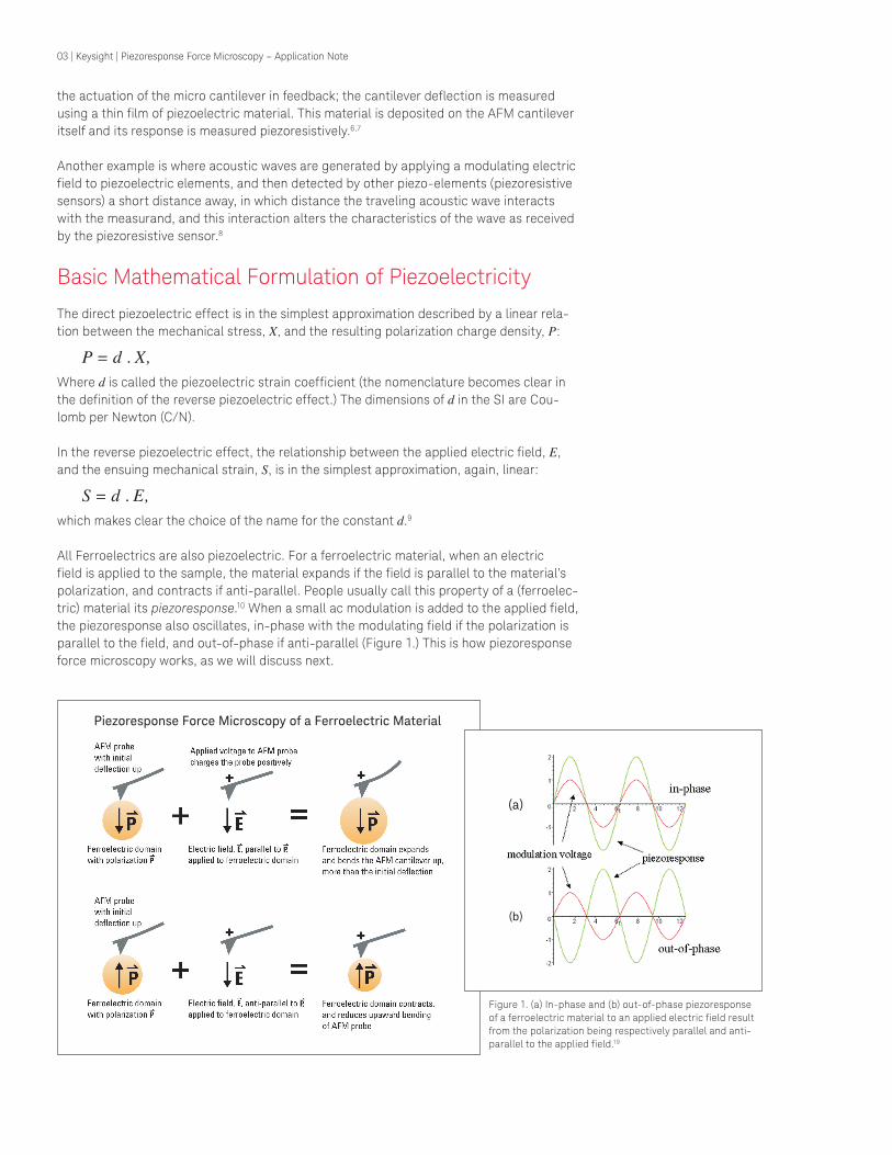
All Ferroelectrics are also piezoelectric. For a ferroelectric material, when an electric field is applied to the sample, the material expands if the field is parallel to the material’s polarization, and contracts if anti-parallel. People usually call this property of a (ferroelec-tric) material its piezoresponse.10 When a small ac modulation is added to the applied field, the piezoresponse also oscillates, in-phase with the modulating field if the polarization is parallel to the field, and out-of-phase if anti-parallel (Figure 1.) This is how piezoresponse force microscopy works, as we will discuss next.
Figure 1. (a) In-phase and (b) out-of-phase piezoresponse of a ferroelectric material to an applied electric field result from the polarization being respectively parallel and anti-parallel to the applied field.19
Piezoresponse Force Microscopy of a Ferroelectric Material
(a)
(b)
03 | Keysight | Piezoresponse Force Microscopy – Application Note
Piezoresponse Force Microscopy
Piezoresponse Force Microscopy (PFM) is a scanning probe microscopy (SPM) technique based on the reverse piezoelectric effect, where a (piezoelectric) material expands or contracts upon applying to it an electric field.11
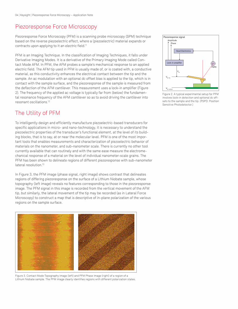
PFM is an Imaging Technique. In the classification of Imaging Techniques, it falls under Derivative Imaging Modes. It is a derivative of the Primary Imaging Mode called Con-tact Mode AFM. In PFM, the AFM probes a sample’s mechanical response to an applied electric field. The AFM tip used in PFM is usually made of, or is coated with, a conductive material, as this conductivity enhances the electrical contact between the tip and the sample. An ac modulation with an optional dc offset bias is applied to the tip, which is in contact with the sample surface, and the piezoresponse of the sample is measured from the deflection of the AFM cantilever. This measurement uses a lock-in amplifier (Figure 2). The frequency of the applied ac voltage is typically far from (below) the fundamen-tal resonance frequency of the AFM cantilever so as to avoid driving the cantilever into resonant oscillations.12
The Utility of PFM
To intelligently design and efficiently manufacture piezoelectric-based transducers for specific applications in micro- and nano-technology, it is necessary to understand the piezoelectric properties of the transducer’s functional element, at the level of its build-ing blocks, that is to say, at or near the molecular level. PFM is one of the most impor-tant tools that enables measurements and characterization of piezoelectric behavior of materials on the nanometer, and sub-nanometer scale. There is currently no other tool currently available that can routinely and with the same ease measure the electrome-chanical response of a material on the level of individual nanometer-scale grains. The PFM has been shown to delineate regions of different piezoresponse with sub-nanometer lateral resolution.13
In Figure 3, the PFM image (phase signal, right image) shows contrast that delineates regions of differing piezoresponse on the surface of a Lithium Niobate sample, whose topography (left image) reveals no features corresponding to those in the piezoresponse image. The PFM signal in this image is recorded from the vertical movement of the AFM tip, but similarly, the lateral movement of the tip may be recorded (as in Lateral Force Microscopy) to construct a map that is descriptive of in-plane polarization of the various regions on the sample surface.
Figure 3. Contact Mode Topography image (left) and PFM Phase image (right) of a region of a Lithium Niobate sample. The PFM image clearly identifies regions with different polarization states.
Figure 2. A typical experimental setup for PFM involves lock-in detection and optional dc off-sets to the sample and the tip. (PSPD: Position Sensitive Photodetector.)
Head Electronics
Piezoresponse signalAmplitude
Phase
Vac
PSPD
Vdc-tip
Vdc-sample
Lock-in amplifier
04 | Keysight | Piezoresponse Force Microscopy – Application Note

PFM has already proved uniquely useful in investigating the nanometer-scale piezo-electric properties of ferroelectrics. Ferroelectric thin films are the subject of intense research and development for their optoelectronic, sensor, and especially high-density memory applications. Since all ferroelectrics are also piezoelectric, much can be learned about the ferroelectric properties, including piezoresponse. The lateral resolution of PFM provides highly localized information about the electromechanical behavior of thin fer-roelectric films (Figure 4).
Figure 4. Contact Mode Topography image (left) and PFM Phase image (right) of domains on a thin film of ferroelectric (courtesy Louis Pacheco, Scientec, Fr.)
For example, as thin films of ferroelectric materials are grown from isolated islands on metal substrates (e.g., for high-density memory applications), one key question to be answered is, at what point during the growth of the thin film is ferroelectricity present. To this end, the PFM can be used to interrogate a given nanometer-scale domain in an island for its piezoelectric response; if there is a piezo response, this implies ferroelec-tricity.14
PFM Spectroscopy is a non-imaging technique that compliments PFM imaging. In PFM Spectroscopy, the piezoresponse of a given location on the sample can be mapped versus, for example, the dc bias (Vdc-tip, Figure 2), or the frequency of the ac signal (Vac, Figure 2) applied to the sample via the tip. This technique can also be used to study hys-teretic characteristics of the piezoresponse.15,16
Summary
The piezoelectric effects, reverse and direct, are now known to be present in materi-als that belong to a wide range of material groups, including polymers, biomaterials17, wood18, ceramics, and non-metallic crystalline solids whose crystal structure has no symmetric center.
With the growing interest in the utility of piezoelectricity and its many manifestations on the nanometer scale, Piezoresponse Force Microscopy has become recognized as a key tool in advancing the research and development of applications based on piezoelectric materials in general, and and the industrially important ferroelectrics.
05 | Keysight | Piezoresponse Force Microscopy – Application Note

References1. P. and J. Curie, Comptes Rendus, 91, 294 (1880).
2. W. G. Hankel, Abh. Sä chs., 12, 457 (1881).
3. This bound polarization surface charge density of piezoelectric origin appears in addition to any that may be present resulting from the dielectric response of the material to an applied field.
4. M. G. Lippmann, Ann. Chimie et Phys. 24, 145 (1881).
5. Piezoelectric Ceramics, Ferroxcube Corporation, Saugerties, NY, USA, © N.V. Philips’ Gloeilampen-fabrieken, Eindhoven, The Netherlands, (1968, 1974).
6. Bringing Scanning Probe Microscopy Up to Speed, S. C. Minne, S. R. Manalis, C.F Quate, Kluwer Academic Publishers, Boston, Dordrecht, London, (1999).
7. Piezoresistive sensors are based on the piezoelectric effect, but work differently from piezoelectric sensors. In piezoelectric sensors, what is detected is the induced polarization charge that comes about due to the mechanical stress. This method does not require a power supply, and for this reason a piezoelectric sensor categorizes as an active sensor. In piezoresistive sensors, by contrast, the electrical resistance of a biased piezoelectric element (usually a thin film) is detected as the measur-and interacts with that element and changes its electrical resistance. Piezoresistive sensors are passive sensors, requiring an external source of power. Zinc oxide (ZnO) is frequently used for its piezoresistive response.
8. Smart Sensors and MEMS, Sergey Y. Yurish and Maria Teresa S.R. Gomes editors, Nato Science Series, II. Mathematics, Physics and Chemistry, Volume 181, Chapter 3. Kluwer Academic Publishers, Dordrecht/Boston/London (2004).
9. Piezoelectric Transducers and Applications, A. Arnau, Editor, Springer-Verlag Berlin Heidelberg, (2004).
10. Piezoresponse Force Microscopy (PFM) was initially developed to investigate ferroelectric materials. In fact, the term piezoresponse as described here (and PFM) appear to be intimately associated with the term ferroelectric in the great majority of published literature so far. Since piezoelectricity is not restricted to ferroelectrics, however, PFM is finding applications beyond ferroelectrics. Although the loose definition of the word piezoresponse does not apply to non-ferroelectrics, PFM is now used to include AFM-based investigation of nanometer-scale electromechanical response of any material to an applied voltage.
11. The acronym PFM is also used for pulse force microscopy, which is entirely different from piezore-sponse force microscopy.
12. A. Gruverman, O. Auciello, H. Tokumoto, Annual Review of Material Science, pp. 101-123, (1998).
13. S. V. Kalinin, B. J. Rodriguez, S. Jesse, T. Thundat, A. Gruverman, Electromechanical imaging of biological systems with sub-10 nm resolution, Appl. Phys. Lett. 87, 053901 (2005).
14. Ferroelectric Thin Films, Basic Properties and Device Physics for Memory Applications, M. Okuyama, Y. Ishibashi, editors, Number 98 in Topics in Applied Physics Series, Springer-Verlag Publishing Com-pany, Germany (2005). See sections 3 and 5.2 in the chapter on “Pb-based Ferroelectric Thin Films Prepared by MOCVD.”
15. M. Alexe, et.al., Applied Physics Letters, 75, 1158, (1999).
16. A. Roelofs, et. al., Applied Physics Letters, 77, 3444, (2000).
17. E. Fukada, I. Yasuda, J. Phys. Soc. Jpn. 12, 1158 (1957). L. Yasuda, J. Jpn. Orthop. Surg. Soc. 28, 267 (1957). E. Fukada, J. Phys. Jpn. 10, 149 (1955).
18. Piezoelectric properties of wood, by V.A. Bazhenov, Consultants Burea, New York, (1961).
19. Graphics adapted from Brian Joseph Rodriguez, PhD Dissertation. Nanoscale investigation of the piezoelectric properties of perovskite ferroelectrics and III-nitrides. North Carolina State University, Department of Physics, (2003).
06 | Keysight | Piezoresponse Force Microscopy – Application Note
This information is subject to change without notice.© Keysight Technologies, 2007 - 2014Published in USA, July 31, 20145989-7611ENwww.keysight.com
For more information on Keysight Technologies’ products, applications or services, please contact your local Keysight office. The complete list is available at:www.keysight.com/find/contactus
Americas Canada (877) 894 4414Brazil 55 11 3351 7010Mexico 001 800 254 2440United States (800) 829 4444
Asia PacificAustralia 1 800 629 485China 800 810 0189Hong Kong 800 938 693India 1 800 112 929Japan 0120 (421) 345Korea 080 769 0800Malaysia 1 800 888 848Singapore 1 800 375 8100Taiwan 0800 047 866Other AP Countries (65) 6375 8100
Europe & Middle EastAustria 0800 001122Belgium 0800 58580Finland 0800 523252France 0805 980333Germany 0800 6270999Ireland 1800 832700Israel 1 809 343051Italy 800 599100Luxembourg +32 800 58580Netherlands 0800 0233200Russia 8800 5009286Spain 800 000154Sweden 0200 882255Switzerland 0800 805353
Opt. 1 (DE)Opt. 2 (FR)Opt. 3 (IT)
United Kingdom 0800 0260637
For other unlisted countries:www.keysight.com/find/contactus(BP-09-23-14)
AFM Instrumentation from Keysight TechnologiesKeysight Technologies offers high-precision, modular AFM solutions for research, industry, and education. Exceptional worldwide support is provided by experienced application scientists and technical service personnel. Keysight’s leading-edge R&D laboratories are dedicated to the timely introduction and optimization of innovative and easy-to-use AFM technologies.www.keysight.com/find/afm