jzy7115l 15a dc-dc intelligent pol 3v to 13.2v input 0.5v
TRANSCRIPT
www.cd4power.com Page 1 of 34
JZY7115L 15A DC-DC Intelligent POL
3V to 13.2V Input • 0.5V to 5.5V Output
Applications • Low voltage, high density systems with
Intermediate Bus Architectures (IBA) • Point-of-load regulators for high performance DSP,
FPGA, ASIC, and microprocessor applications • Desktops, servers, and portable computing • Broadband, networking, optical, and
communications systems • Active memory bus terminators Benefits • Integrates digital power conversion with intelligent
power management • Eliminates the need for external power
management components • Completely programmable via industry standard
serial communication bus • One part that covers all applications • Reduces board space, system cost and
complexity, and time to market
Features • Wide input voltage range: 3V – 13.2V • High continuous output current: 15A • Active digital current share • Single-wire serial communication bus for frequency
synchronization, programming, and monitoring • Wide programmable output voltage range: 0.5V to
5.5V • Optimal voltage positioning with programmable slope
of the VI line • Overcurrent, overvoltage, undervoltage, and
overtemperature protections with programmable thresholds and types
• Programmable fixed switching frequency 0.5-1.0MHz • Programmable turn-on and turn-off delays • Programmable turn-on and turn-off voltage slew rates
with tracking protection • Programmable feedback loop compensation • Power Good signal with programmable limits • Programmable fault management • Start up into the load pre-biased up to 100% • Full rated current sink • Real time voltage, current, and temperature
measurements, monitoring, and reporting • Small footprint vertical SMT package: 8x32mm • Low profile of 14mm • Compatible with conventional pick-and-place
equipment • Wide operating temperature range • UL60950 recognized, CSA C22.2 No. 60950-00
certified, and TUV EN60950-1:2001 certified
Description The JZY7115L is an intelligent, fully programmable step-down point-of-load DC-DC module integrating digital power conversion and intelligent power management. When used with JZM7100 Series Digital Power Managers, the JZY7115L completely eliminates the need for external components for sequencing, tracking, protection, monitoring, and reporting. All parameters of the JZY7115L are programmable via the serial communication bus and can be changed by a user at any time during product development and service. Selection Chart
Model Input Voltage Range (VDC)
Output Voltage Range (VDC)
Output Voltage Setpoint Accuracy (%VOUT or mV, whichever is greater)
Output Current (ADC)
JZY7115L 3.0 – 13.2 0.5 – 5.5 1% or 20mV 15
www.cd4power.com Page 2 of 34
JZY7115L 15A DC-DC Intelligent POL
3V to 13.2V Input • 0.5V to 5.5V Output
1. Reference Documents: • JZM7100 Digital Power Manager. Data Sheet • Digital Power Manager. Programming Manual • ZIOSTM Graphical User Interface
2. Ordering Information • JZY7117L
3. Absolute Maximum Ratings Stresses in excess of the absolute maximum ratings may cause performance degradation, adversely affect long-term reliability, and cause permanent damage to the converter.
Parameter Conditions/Description Min Max Units
Operating Temperature Controller case temperature -40 105 °C
Input Voltage 250ms Transient 15 VDC
Output Current (See Output Current Derating Curves) -15 15 ADC
4. Environmental and Mechanical Specifications
Parameter Conditions/Description Min Nom Max Units
Ambient Temperature Range -40 85 °C
Storage Temperature (Ts) -55 125 °C
Weight 15 grams
MTBF Calculated Per Telcordia Technologies SR-332 4.82 MHrs 1) DC-DC Front End suffix: HBC for HBC25ZH-NT; QBC for QBC11ZH-NT; HDS for HDS48T30120-NCAR; QHS for QHS25ZG-NT
www.cd4power.com Page 3 of 34
JZY7115L 15A DC-DC Intelligent POL
3V to 13.2V Input • 0.5V to 5.5V Output
5. Electrical Specifications Specifications apply at the input voltage from 3V to 13.2V, output load from 0 to 15A, ambient temperature from -40°C to 85°C, and default performance parameters settings unless otherwise noted.
5.1 Input Specifications Parameter Conditions/Description Min Nom Max Units
Input voltage (VIN) At VIN<4.75V, VLDO pin needs to be
connected to an external voltage source higher than 4.75V
3 13.2 VDC
Input Current (at no load) VIN≥4.75V, VLDO pin connected to VIN 50 mADC
Undervoltage Lockout (VLDO connected to VIN)
Ramping Up Ramping Down 4.2
3.75 VDC VDC
Undervoltage Lockout (VLDO connected to VAUX=5V)
Ramping Up Ramping Down 3.0
2.5 VDC VDC
External Low Voltage Supply Connect to VLDO pin when VIN<4.75V 4.75 13.2 VDC
VLDO Input Current Current drawn from the external low voltage supply at VLDO=5V 50 mADC
5.2 Output Specifications Parameter Conditions/Description Min Nom Max Units
Output Voltage Range (VOUT) Programmable1 Default (no programming)
0.5
0.5
5.5
VDC VDC
Output Voltage Setpoint Accuracy VIN=12V, IOUT=0.5*IOUT MAX, FSW=500kHz, room temperature (See Selection Chart)
Output Current (IOUT) VIN MIN to VIN MAX -152 15 ADC
Line Regulation VIN MIN to VIN MAX ±0.3 %VOUT
Load Regulation 0 to IOUT MAX ±0.2 %VOUT Dynamic Regulation
Peak Deviation Settling Time
Slew rate 2.5A/μs, 50 -100% load stepCOUT=300μF, FSW=1MHz to 10% of peak deviation
100 50
mV μs
Output Voltage Peak-to-Peak Ripple and Noise
BW=20MHz With external capacitance
VIN=5.0V, VOUT=0.5V, FSW=500kHz VIN=13.2V, VOUT=0.5V, FSW=500kHz VIN=5.0V, VOUT=2.5V, FSW=500kHz VIN=13.2V, VOUT=2.5V, FSW=500kHz VIN=13.2V, VOUT=5.0V, FSW=500kHz
10 15 10 25 35
mV mV mV mV mV
Temperature Coefficient VIN=12V, IOUT=0.5*IOUT MAX 20 ppm/°C
Switching Frequency Default Programmable, 250kHz steps
500
500
1,000
kHz kHz
Duty Cycle Limit Default Programmable, 1.56% steps
0
90.5
95
% %
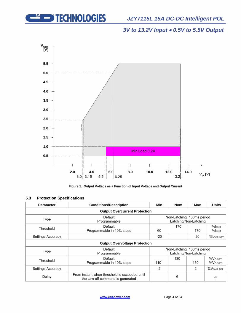
1 JZY7115L is a step-down converter, thus the output voltage is always lower than the input voltage as show in Figure 1. 2 At the negative output current (bus terminator mode) efficiency of the JZY7115L degrades resulting in increased internal power dissipation. Therefore maximum allowable negative current under specific conditions is 20% lower than the current determined from the derating curves shown in paragraph 6.5.
www.cd4power.com Page 4 of 34
JZY7115L 15A DC-DC Intelligent POL
3V to 13.2V Input • 0.5V to 5.5V Output
5.0
4.0
3.0
2.0
1.0
VOUT[V]
14.012.010.08.06.02.0 4.0
Min Load 0.2A
VIN [V]3.0 3.15 13.25.5
2.5
5.5
4.5
3.5
1.5
0.5
6.25
Figure 1. Output Voltage as a Function of Input Voltage and Output Current
5.3 Protection Specifications Parameter Conditions/Description Min Nom Max Units
Output Overcurrent Protection
Type Default Programmable
Non-Latching, 130ms period Latching/Non-Latching
Threshold Default Programmable in 10% steps
60
170
170
%IOUT %IOUT
Settings Accuracy -20 20 %IOCP.SET
Output Overvoltage Protection
Type Default Programmable
Non-Latching, 130ms period Latching/Non-Latching
Threshold Default Programmable in 10% steps
1101
130
130
%VO.SET %VO.SET
Settings Accuracy -2 2 %VOVP.SET
Delay From instant when threshold is exceeded until the turn-off command is generated 6 μs
www.cd4power.com Page 5 of 34
JZY7115L 15A DC-DC Intelligent POL
3V to 13.2V Input • 0.5V to 5.5V Output
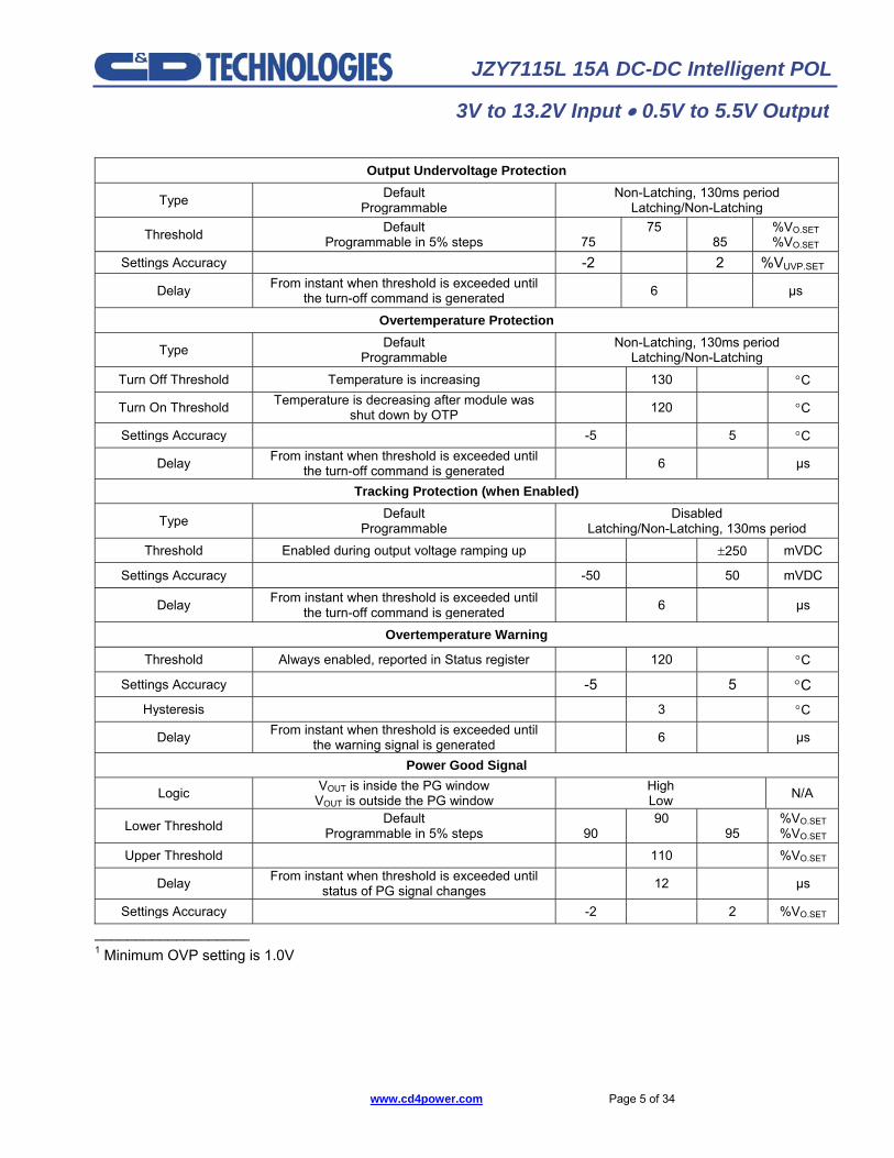
Output Undervoltage Protection
Type Default Programmable
Non-Latching, 130ms period Latching/Non-Latching
Threshold Default Programmable in 5% steps
75
75
85
%VO.SET %VO.SET
Settings Accuracy -2 2 %VUVP.SET
Delay From instant when threshold is exceeded until the turn-off command is generated 6 μs
Overtemperature Protection
Type Default Programmable
Non-Latching, 130ms period Latching/Non-Latching
Turn Off Threshold Temperature is increasing 130 °C
Turn On Threshold Temperature is decreasing after module was shut down by OTP 120 °C
Settings Accuracy -5 5 °C
Delay From instant when threshold is exceeded until the turn-off command is generated 6 μs
Tracking Protection (when Enabled)
Type Default Programmable
Disabled Latching/Non-Latching, 130ms period
Threshold Enabled during output voltage ramping up ±250 mVDC
Settings Accuracy -50 50 mVDC
Delay From instant when threshold is exceeded until the turn-off command is generated 6 μs
Overtemperature Warning
Threshold Always enabled, reported in Status register 120 °C
Settings Accuracy -5 5 °C Hysteresis 3 °C
Delay From instant when threshold is exceeded until the warning signal is generated 6 μs
Power Good Signal
Logic VOUT is inside the PG window VOUT is outside the PG window
High Low N/A
Lower Threshold Default Programmable in 5% steps
90
90
95
%VO.SET %VO.SET
Upper Threshold 110 %VO.SET
Delay From instant when threshold is exceeded until status of PG signal changes 12 μs
Settings Accuracy -2 2 %VO.SET ___________________ 1 Minimum OVP setting is 1.0V
www.cd4power.com Page 6 of 34
JZY7115L 15A DC-DC Intelligent POL
3V to 13.2V Input • 0.5V to 5.5V Output
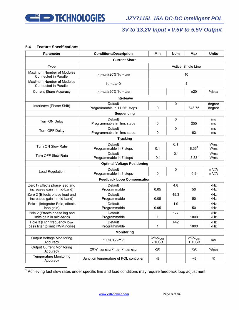
5.4 Feature Specifications Parameter Conditions/Description Min Nom Max Units
Current Share
Type Active, Single Line
Maximum Number of Modules Connected in Parallel IOUT MIN≥20%*IOUT NOM 10
Maximum Number of Modules Connected in Parallel IOUT MIN=0 4
Current Share Accuracy IOUT MIN≥20%*IOUT NOM ±20 %IOUT
Interleave
Interleave (Phase Shift) Default Programmable in 11.25° steps
0
0
348.75
degree degree
Sequencing
Turn ON Delay Default Programmable in 1ms steps
0
0
255
ms ms
Turn OFF Delay Default Programmable in 1ms steps
0
0
63
ms ms
Tracking
Turn ON Slew Rate Default Programmable in 7 steps
0.1
0.1
8.331
V/ms V/ms
Turn OFF Slew Rate Default Programmable in 7 steps
-0.1
-0.1
-8.331
V/ms V/ms
Optimal Voltage Positioning
Load Regulation Default Programmable in 8 steps
0
0
6.9
mV/A mV/A
Feedback Loop Compensation Zero1 (Effects phase lead and
increases gain in mid-band) Default
Programmable
0.05 4.8
50 kHz kHz
Zero 2 (Effects phase lead and increases gain in mid-band)
Default Programmable
0.05
49.3
50
kHz kHz
Pole 1 (Integrator Pole, effects loop gain)
Default Programmable
0.05
1.9
50
kHz kHz
Pole 2 (Effects phase lag and limits gain in mid-band)
Default Programmable
1
177
1000
kHz kHz
Pole 3 (High frequency low- pass filter to limit PWM noise)
Default Programmable
1
442
1000
kHz kHz
Monitoring Output Voltage Monitoring
Accuracy 1 LSB=22mV -2%VOUT - 1LSB 2%VOUT
+ 1LSB mV
Output Current Monitoring Accuracy 20%*IOUT NOM < IOUT < IOUT NOM -20 +20 %IOUT
Temperature Monitoring Accuracy Junction temperature of POL controller -5 +5 °C
___________________ 1 Achieving fast slew rates under specific line and load conditions may require feedback loop adjustment
www.cd4power.com Page 7 of 34
JZY7115L 15A DC-DC Intelligent POL
3V to 13.2V Input • 0.5V to 5.5V Output
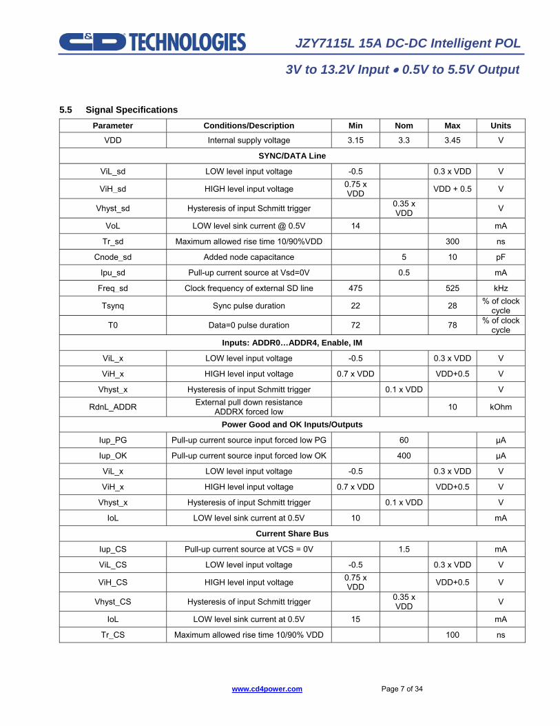
5.5 Signal Specifications Parameter Conditions/Description Min Nom Max Units
VDD Internal supply voltage 3.15 3.3 3.45 V
SYNC/DATA Line
ViL_sd LOW level input voltage -0.5 0.3 x VDD V
ViH_sd HIGH level input voltage 0.75 x VDD VDD + 0.5 V
Vhyst_sd Hysteresis of input Schmitt trigger 0.35 x VDD V
VoL LOW level sink current @ 0.5V 14 mA
Tr_sd Maximum allowed rise time 10/90%VDD 300 ns
Cnode_sd Added node capacitance 5 10 pF
Ipu_sd Pull-up current source at Vsd=0V 0.5 mA
Freq_sd Clock frequency of external SD line 475 525 kHz
Tsynq Sync pulse duration 22 28 % of clock cycle
T0 Data=0 pulse duration 72 78 % of clock cycle
Inputs: ADDR0…ADDR4, Enable, IM
ViL_x LOW level input voltage -0.5 0.3 x VDD V
ViH_x HIGH level input voltage 0.7 x VDD VDD+0.5 V
Vhyst_x Hysteresis of input Schmitt trigger 0.1 x VDD V
RdnL_ADDR External pull down resistance ADDRX forced low 10 kOhm
Power Good and OK Inputs/Outputs
Iup_PG Pull-up current source input forced low PG 60 μA
Iup_OK Pull-up current source input forced low OK 400 μA
ViL_x LOW level input voltage -0.5 0.3 x VDD V
ViH_x HIGH level input voltage 0.7 x VDD VDD+0.5 V
Vhyst_x Hysteresis of input Schmitt trigger 0.1 x VDD V
IoL LOW level sink current at 0.5V 10 mA
Current Share Bus
Iup_CS Pull-up current source at VCS = 0V 1.5 mA
ViL_CS LOW level input voltage -0.5 0.3 x VDD V
ViH_CS HIGH level input voltage 0.75 x VDD VDD+0.5 V
Vhyst_CS Hysteresis of input Schmitt trigger 0.35 x VDD V
IoL LOW level sink current at 0.5V 15 mA
Tr_CS Maximum allowed rise time 10/90% VDD 100 ns
www.cd4power.com Page 8 of 34
JZY7115L 15A DC-DC Intelligent POL
3V to 13.2V Input • 0.5V to 5.5V Output
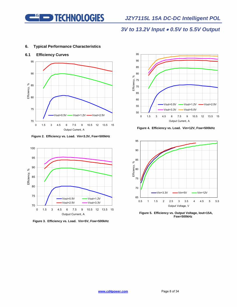
6. Typical Performance Characteristics
6.1 Efficiency Curves
70
75
80
85
90
95
0 1.5 3 4.5 6 7.5 9 10.5 12 13.5 15
Output Current, A
Effi
cien
cy, %
Vout=0.5V Vout=1.2V Vout=2.5V
Figure 2. Efficiency vs. Load. Vin=3.3V, Fsw=500kHz
70
75
80
85
90
95
100
0 1.5 3 4.5 6 7.5 9 10.5 12 13.5 15Output Current, A
Effic
ienc
y, %
Vout=0.5V Vout=1.2VVout=2.5V Vout=3.3V
Figure 3. Efficiency vs. Load. Vin=5V, Fsw=500kHz
50
55
60
65
70
75
80
85
90
95
0 1.5 3 4.5 6 7.5 9 10.5 12 13.5 15
Output Current, A
Effi
cien
cy, %
Vout=0.5V Vout=1.2V Vout=2.5V
Vout=3.3V Vout=5.0V
Figure 4. Efficiency vs. Load. Vin=12V, Fsw=500kHz
65
70
75
80
85
90
95
0.5 1 1.5 2 2.5 3 3.5 4 4.5 5 5.5
Output Voltage, V
Effi
cien
cy, %
Vin=3.3V Vin=5V Vin=12V
Figure 5. Efficiency vs. Output Voltage, Iout=15A,
Fsw=500kHz
www.cd4power.com Page 9 of 34
JZY7115L 15A DC-DC Intelligent POL
3V to 13.2V Input • 0.5V to 5.5V Output
65
70
75
80
85
90
95
3 4 5 6 7 8 9 10 11 12Input Voltage, V
Effi
cien
cy, %
Vout=0.5V Vout=1.2VVout=2.5V Vout=3.3V
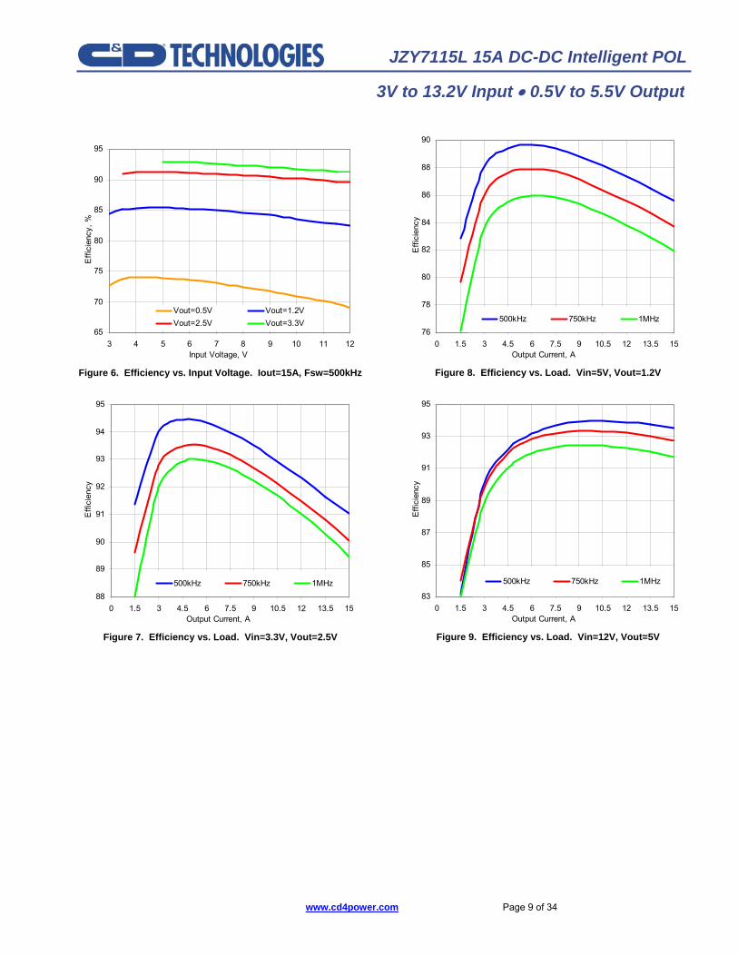
Figure 6. Efficiency vs. Input Voltage. Iout=15A, Fsw=500kHz
88
89
90
91
92
93
94
95
0 1.5 3 4.5 6 7.5 9 10.5 12 13.5 15Output Current, A
Effi
cien
cy
500kHz 750kHz 1MHz
Figure 7. Efficiency vs. Load. Vin=3.3V, Vout=2.5V
76
78
80
82
84
86
88
90
0 1.5 3 4.5 6 7.5 9 10.5 12 13.5 15Output Current, A
Effi
cien
cy
500kHz 750kHz 1MHz
Figure 8. Efficiency vs. Load. Vin=5V, Vout=1.2V
83
85
87
89
91
93
95
0 1.5 3 4.5 6 7.5 9 10.5 12 13.5 15Output Current, A
Effi
cien
cy
500kHz 750kHz 1MHz
Figure 9. Efficiency vs. Load. Vin=12V, Vout=5V
www.cd4power.com Page 10 of 34
JZY7115L 15A DC-DC Intelligent POL
3V to 13.2V Input • 0.5V to 5.5V Output
80
82
84
86
88
90
92
94
500 750 1000
Switching Frequency, kHz
Effi
cien
cy
3.3Vin/2.5Vout 5Vin/1.2Vout 12Vin/5Vout
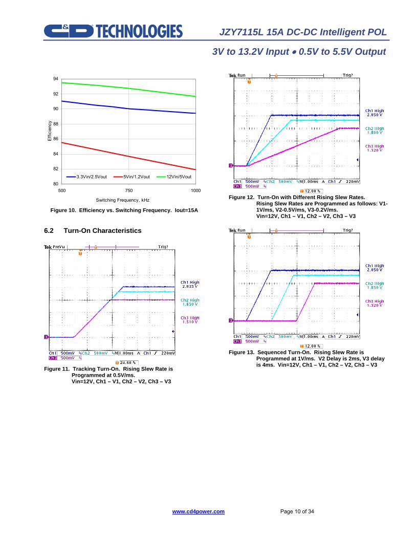
Figure 10. Efficiency vs. Switching Frequency. Iout=15A
6.2 Turn-On Characteristics
Figure 11. Tracking Turn-On. Rising Slew Rate is
Programmed at 0.5V/ms. Vin=12V, Ch1 – V1, Ch2 – V2, Ch3 – V3
Figure 12. Turn-On with Different Rising Slew Rates.
Rising Slew Rates are Programmed as follows: V1-1V/ms, V2-0.5V/ms, V3-0.2V/ms. Vin=12V, Ch1 – V1, Ch2 – V2, Ch3 – V3
Figure 13. Sequenced Turn-On. Rising Slew Rate is
Programmed at 1V/ms. V2 Delay is 2ms, V3 delay is 4ms. Vin=12V, Ch1 – V1, Ch2 – V2, Ch3 – V3
www.cd4power.com Page 11 of 34
JZY7115L 15A DC-DC Intelligent POL
3V to 13.2V Input • 0.5V to 5.5V Output
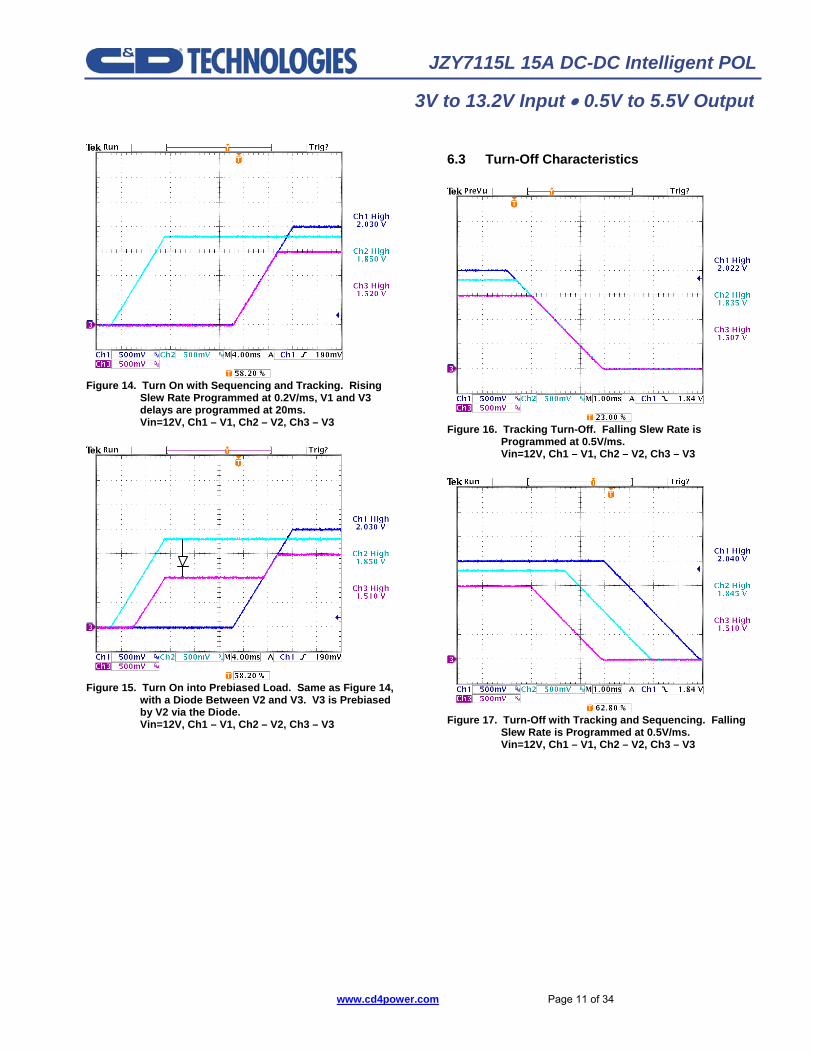
Figure 14. Turn On with Sequencing and Tracking. Rising
Slew Rate Programmed at 0.2V/ms, V1 and V3 delays are programmed at 20ms. Vin=12V, Ch1 – V1, Ch2 – V2, Ch3 – V3
Figure 15. Turn On into Prebiased Load. Same as Figure 14,
with a Diode Between V2 and V3. V3 is Prebiased by V2 via the Diode. Vin=12V, Ch1 – V1, Ch2 – V2, Ch3 – V3
6.3 Turn-Off Characteristics
Figure 16. Tracking Turn-Off. Falling Slew Rate is
Programmed at 0.5V/ms. Vin=12V, Ch1 – V1, Ch2 – V2, Ch3 – V3
Figure 17. Turn-Off with Tracking and Sequencing. Falling
Slew Rate is Programmed at 0.5V/ms. Vin=12V, Ch1 – V1, Ch2 – V2, Ch3 – V3
www.cd4power.com Page 12 of 34
JZY7115L 15A DC-DC Intelligent POL
3V to 13.2V Input • 0.5V to 5.5V Output
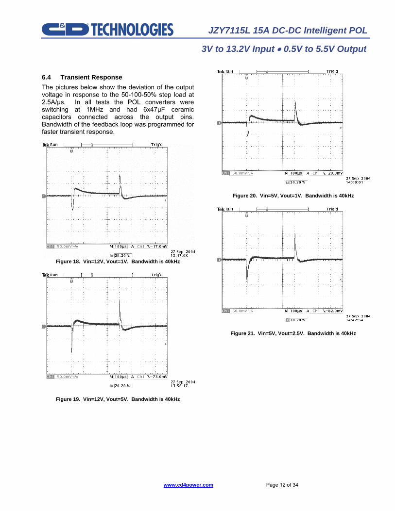
6.4 Transient Response The pictures below show the deviation of the output voltage in response to the 50-100-50% step load at 2.5A/μs. In all tests the POL converters were switching at 1MHz and had 6x47μF ceramic capacitors connected across the output pins. Bandwidth of the feedback loop was programmed for faster transient response.
Figure 18. Vin=12V, Vout=1V. Bandwidth is 40kHz
Figure 19. Vin=12V, Vout=5V. Bandwidth is 40kHz
Figure 20. Vin=5V, Vout=1V. Bandwidth is 40kHz
Figure 21. Vin=5V, Vout=2.5V. Bandwidth is 40kHz
www.cd4power.com Page 13 of 34
JZY7115L 15A DC-DC Intelligent POL
3V to 13.2V Input • 0.5V to 5.5V Output
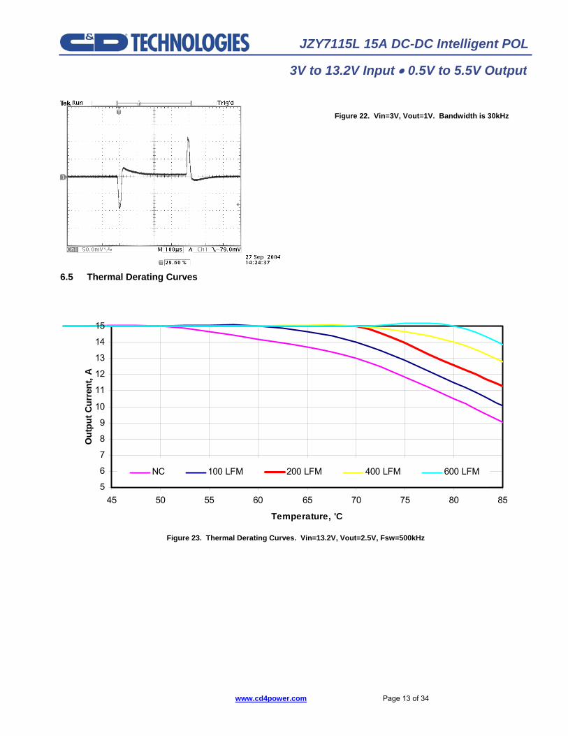
Figure 22. Vin=3V, Vout=1V. Bandwidth is 30kHz
6.5 Thermal Derating Curves
5
6
7
8
9
10
11
12
13
14
15
45 50 55 60 65 70 75 80 85
Temperature, 'C
Out
put C
urre
nt, A
NC 100 LFM 200 LFM 400 LFM 600 LFM
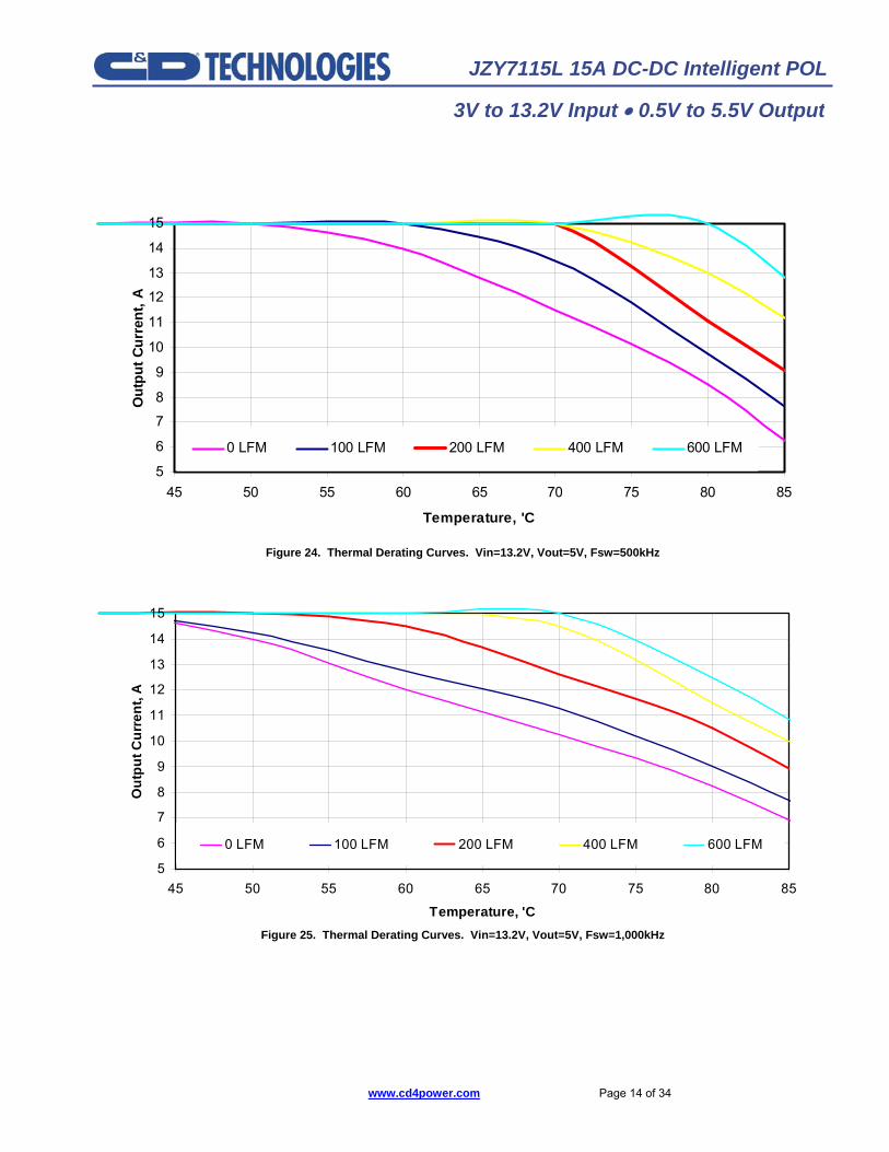
Figure 23. Thermal Derating Curves. Vin=13.2V, Vout=2.5V, Fsw=500kHz
www.cd4power.com Page 14 of 34
JZY7115L 15A DC-DC Intelligent POL
3V to 13.2V Input • 0.5V to 5.5V Output
5
6
7
8
9
10
11
12
13
14
15
45 50 55 60 65 70 75 80 85
Temperature, 'C
Out
put C
urre
nt, A
0 LFM 100 LFM 200 LFM 400 LFM 600 LFM
Figure 24. Thermal Derating Curves. Vin=13.2V, Vout=5V, Fsw=500kHz
5
6
7
8
9
10
11
12
13
14
15
45 50 55 60 65 70 75 80 85
Temperature, 'C
Out
put C
urre
nt, A
0 LFM 100 LFM 200 LFM 400 LFM 600 LFM
Figure 25. Thermal Derating Curves. Vin=13.2V, Vout=5V, Fsw=1,000kHz
www.cd4power.com Page 15 of 34
JZY7115L 15A DC-DC Intelligent POL
3V to 13.2V Input • 0.5V to 5.5V Output
7. Typical Application
ZY7115L
V1 V2 V3
CS
SD
OK_A OK_B
ADDR ADDR ADDR ADDR
DPM I2C
Intermediate Voltage Bus
ZY7115L ZY7115L ZY7115L
OK_C
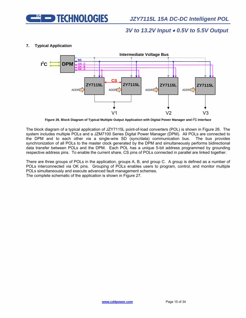
Figure 26. Block Diagram of Typical Multiple Output Application with Digital Power Manager and I2C Interface
The block diagram of a typical application of JZY7115L point-of-load converters (POL) is shown in Figure 26. The system includes multiple POLs and a JZM7100 Series Digital Power Manager (DPM). All POLs are connected to the DPM and to each other via a single-wire SD (sync/data) communication bus. The bus provides synchronization of all POLs to the master clock generated by the DPM and simultaneously performs bidirectional data transfer between POLs and the DPM. Each POL has a unique 5-bit address programmed by grounding respective address pins. To enable the current share, CS pins of POLs connected in parallel are linked together. There are three groups of POLs in the application, groups A, B, and group C. A group is defined as a number of POLs interconnected via OK pins. Grouping of POLs enables users to program, control, and monitor multiple POLs simultaneously and execute advanced fault management schemes. The complete schematic of the application is shown in Figure 27.
www.cd4power.com Page 16 of 34
JZY7115L 15A DC-DC Intelligent POL
3V to 13.2V Input • 0.5V to 5.5V Output
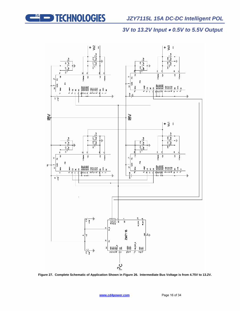
Figure 27. Complete Schematic of Application Shown in Figure 26. Intermediate Bus Voltage is from 4.75V to 13.2V.
www.cd4power.com Page 17 of 34
JZY7115L 15A DC-DC Intelligent POL
3V to 13.2V Input • 0.5V to 5.5V Output
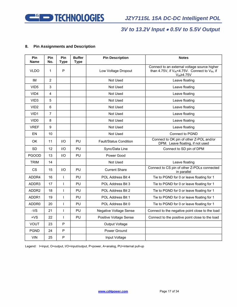
8. Pin Assignments and Description
Pin Name
Pin No.
Pin Type
Buffer Type
Pin Description Notes
VLDO 1 P Low Voltage Dropout Connect to an external voltage source higher than 4.75V, if VIN<4.75V. Connect to VIN, if
VIN≥4.75V IM 2 Not Used Leave floating
VID5 3 Not Used Leave floating
VID4 4 Not Used Leave floating
VID3 5 Not Used Leave floating
VID2 6 Not Used Leave floating
VID1 7 Not Used Leave floating
VID0 8 Not Used Leave floating
VREF 9 Not Used Leave floating
EN 10 Not Used Connect to PGND
OK 11 I/O PU Fault/Status Condition Connect to OK pin of other Z-POL and/or DPM. Leave floating, if not used
SD 12 I/O PU Sync/Data Line Connect to SD pin of DPM
PGOOD 13 I/O PU Power Good
TRIM 14 Not Used Leave floating
CS 15 I/O PU Current Share Connect to CS pin of other Z-POLs connected in parallel
ADDR4 16 I PU POL Address Bit 4 Tie to PGND for 0 or leave floating for 1
ADDR3 17 I PU POL Address Bit 3 Tie to PGND for 0 or leave floating for 1
ADDR2 18 I PU POL Address Bit 2 Tie to PGND for 0 or leave floating for 1
ADDR1 19 I PU POL Address Bit 1 Tie to PGND for 0 or leave floating for 1
ADDR0 20 I PU POL Address Bit 0 Tie to PGND for 0 or leave floating for 1
-VS 21 I PU Negative Voltage Sense Connect to the negative point close to the load
+VS 22 I PU Positive Voltage Sense Connect to the positive point close to the load
VOUT 23 P Output Voltage
PGND 24 P Power Ground
VIN 25 P Input Voltage Legend: I=input, O=output, I/O=input/output, P=power, A=analog, PU=internal pull-up
www.cd4power.com Page 18 of 34
JZY7115L 15A DC-DC Intelligent POL
3V to 13.2V Input • 0.5V to 5.5V Output
9. Programmable Features Performance parameters of JZY7115L POL converters can be programmed via the industry standard I2C communication bus without replacing any components or rewiring PCB traces. Each parameter has a default value stored in the volatile memory registers detailed in Table 1. The setup registers 00h through 14h are programmed at the system power-up. When the user programs new performance parameters, the values in the registers are overwritten. Upon removal of the input voltage, the default values are restored.
Table 1. JZY7115L Memory Registers
Register Content Address PC1 Protection Configuration 1 00h PC2 Protection Configuration 2 01h PC3 Protection Configuration 3 02h DON Turn-On Delay 05h DOF Turn-Off Delay 06h TC Tracking Configuration 03h INT Interleave Configuration and
Frequency Selection 04h
RUN RUN Register 15h ST Status Register 16h
VOS Output Voltage Setpoint 07h CLS Current Limit Setpoint 08h DCL Duty Cycle Limit 09h B1 Dig Controller Denominator z-1
Coefficient 0Ah
B2 Dig Controller Denominator z-2 Coefficient
0Bh
B3 Dig Controller Denominator z-3 Coefficient
0Ch
C0L Dig Controller Numerator z0 Coefficient, Low Byte
0Dh
C0H Dig Controller Numerator z0 Coefficient, High Byte
0Eh
C1L Dig Controller Numerator z-1 Coefficient, Low Byte
0Fh
C1H Dig Controller Numerator z-1 Coefficient, High Byte
10h
C2L Dig Controller Numerator z-2 Coefficient, Low Byte
11h
C2H Dig Controller Numerator z-2 Coefficient, High Byte
12h
C3L Dig Controller Numerator z-3 Coefficient, High Byte
13h
C3H Dig Controller Numerator z-3 Coefficient, Low Byte
14h
VOM Output Voltage Monitoring 17h IOM Output Current Monitoring 18h TMP Temperature Monitoring 19h
JZY7115L converters can be programmed using the ZIOSTM Graphical User Interface or directly via the I2C bus by using high and low level commands as described in the ‘”DPM Programming Manual”. JZY7115L parameters can be reprogrammed at any time during the system operation and service except for the digital filter coefficients, the switching frequency and the duty cycle limit, that can only be changed when the POL is turned off.
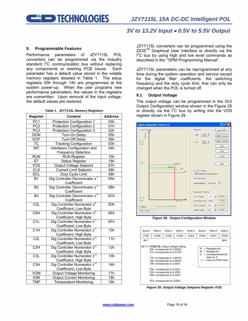
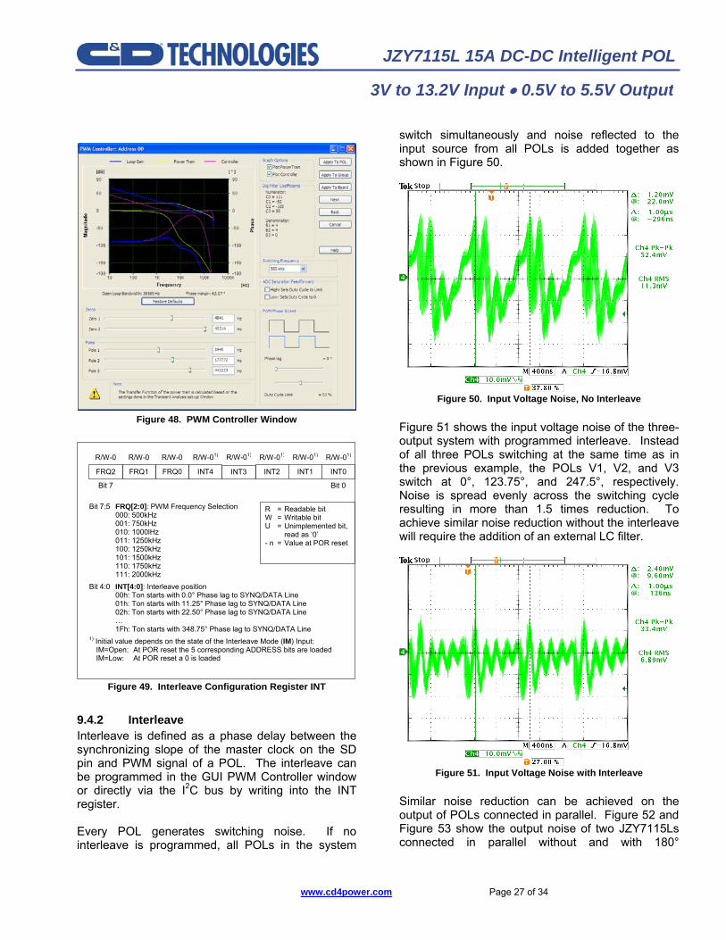
9.1 Output Voltage The output voltage can be programmed in the GUI Output Configuration window shown in the Figure 28 or directly via the I2C bus by writing into the VOS register shown in Figure 29.
Figure 28. Output Configuration Window
VOS7 VOS6 VOS5 VOS4 VOS2 VOS1 VOS0
Bit 7 Bit 0
R = Readable bitW = Writable bitU = Unimplemented bit,
read as ‘0’- n = Value at POR reset
R/W-0 R/W-0 R/W-0 R/W-0 R/W-0 R/W-0 R/W-0R/W-0
Bit 7:0 VOS[7:0], Output voltage setting00h: corresponds to 0.5000V01h: corresponds to 0.5125V…77h: corresponds to 1.9875V78h: corresponds to 2.0000V79h: corresponds to 2.025V…F9h: corresponds to 5.225VFAh: corresponds to 5.250VFBh: corresponds to 5.300V…FFh: corresponds to 5.500V
VOS3
Figure 29. Output Voltage Setpoint Register VOS
www.cd4power.com Page 19 of 34
JZY7115L 15A DC-DC Intelligent POL
3V to 13.2V Input • 0.5V to 5.5V Output
9.1.1 Output Voltage Setpoint The output voltage programming range is from 0.5V to 5.5V. Within this range, there are 256 predefined voltage setpoints. To improve resolution of the output voltage settings, the voltage range is divided into three sub-ranges as shown in Table 2.
Table 2. Output Voltage Adjustment Resolution
VOUT MIN, V VOUT MAX, V Resolution, mV
0.500 2.000 12.5
2.025 5.25 25
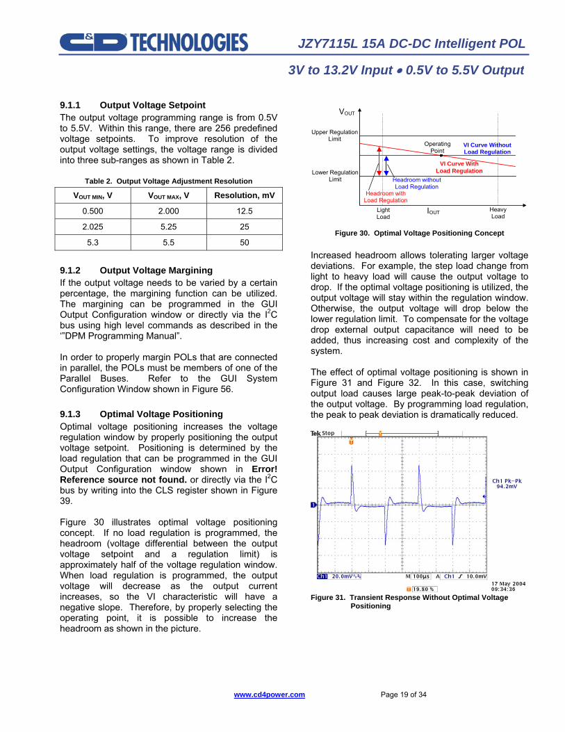
5.3 5.5 50 9.1.2 Output Voltage Margining If the output voltage needs to be varied by a certain percentage, the margining function can be utilized. The margining can be programmed in the GUI Output Configuration window or directly via the I2C bus using high level commands as described in the ‘”DPM Programming Manual”. In order to properly margin POLs that are connected in parallel, the POLs must be members of one of the Parallel Buses. Refer to the GUI System Configuration Window shown in Figure 56. 9.1.3 Optimal Voltage Positioning Optimal voltage positioning increases the voltage regulation window by properly positioning the output voltage setpoint. Positioning is determined by the load regulation that can be programmed in the GUI Output Configuration window shown in Error! Reference source not found. or directly via the I2C bus by writing into the CLS register shown in Figure 39. Figure 30 illustrates optimal voltage positioning concept. If no load regulation is programmed, the headroom (voltage differential between the output voltage setpoint and a regulation limit) is approximately half of the voltage regulation window. When load regulation is programmed, the output voltage will decrease as the output current increases, so the VI characteristic will have a negative slope. Therefore, by properly selecting the operating point, it is possible to increase the headroom as shown in the picture.
Upper RegulationLimit
Lower RegulationLimit
LightLoad
VOUT
IOUT
VI Curve WithoutLoad Regulation
VI Curve WithLoad Regulation
HeavyLoad
Headroom withoutLoad Regulation
OperatingPoint
Headroom withLoad Regulation
Figure 30. Optimal Voltage Positioning Concept
Increased headroom allows tolerating larger voltage deviations. For example, the step load change from light to heavy load will cause the output voltage to drop. If the optimal voltage positioning is utilized, the output voltage will stay within the regulation window. Otherwise, the output voltage will drop below the lower regulation limit. To compensate for the voltage drop external output capacitance will need to be added, thus increasing cost and complexity of the system. The effect of optimal voltage positioning is shown in Figure 31 and Figure 32. In this case, switching output load causes large peak-to-peak deviation of the output voltage. By programming load regulation, the peak to peak deviation is dramatically reduced.
Figure 31. Transient Response Without Optimal Voltage
Positioning
www.cd4power.com Page 20 of 34
JZY7115L 15A DC-DC Intelligent POL
3V to 13.2V Input • 0.5V to 5.5V Output
Figure 32. Transient Response With Optimal Voltage
Positioning
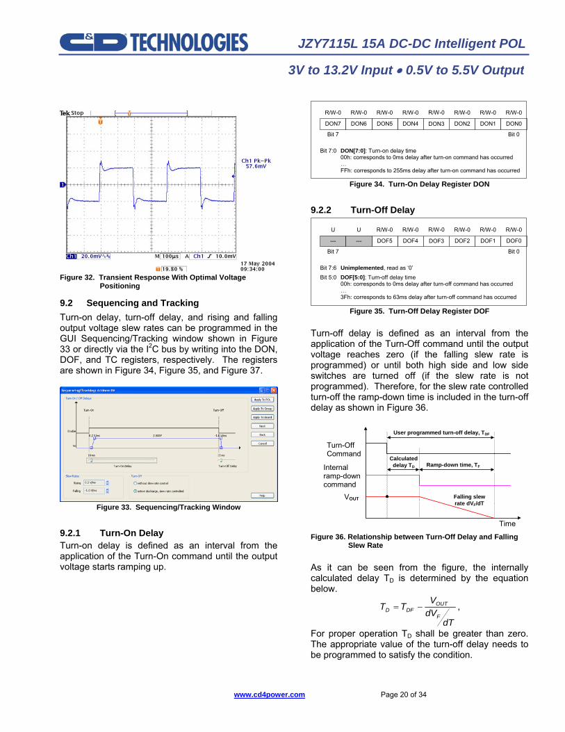
9.2 Sequencing and Tracking Turn-on delay, turn-off delay, and rising and falling output voltage slew rates can be programmed in the GUI Sequencing/Tracking window shown in Figure 33 or directly via the I2C bus by writing into the DON, DOF, and TC registers, respectively. The registers are shown in Figure 34, Figure 35, and Figure 37.
Figure 33. Sequencing/Tracking Window
9.2.1 Turn-On Delay Turn-on delay is defined as an interval from the application of the Turn-On command until the output voltage starts ramping up.
DON7 DON6 DON5 DON4 DON2 DON1 DON0
Bit 7 Bit 0
R/W-0 R/W-0 R/W-0 R/W-0 R/W-0 R/W-0 R/W-0R/W-0
Bit 7:0 DON[7:0]: Turn-on delay time00h: corresponds to 0ms delay after turn-on command has occurred…FFh: corresponds to 255ms delay after turn-on command has occurred
DON3
Figure 34. Turn-On Delay Register DON
9.2.2 Turn-Off Delay
--- --- DOF5 DOF4 DOF2 DOF1 DOF0
Bit 7 Bit 0
U U R/W-0 R/W-0 R/W-0 R/W-0 R/W-0R/W-0
Bit 7:6 Unimplemented, read as ‘0’Bit 5:0 DOF[5:0]: Turn-off delay time
00h: corresponds to 0ms delay after turn-off command has occurred…3Fh: corresponds to 63ms delay after turn-off command has occurred
DOF3
Figure 35. Turn-Off Delay Register DOF
Turn-off delay is defined as an interval from the application of the Turn-Off command until the output voltage reaches zero (if the falling slew rate is programmed) or until both high side and low side switches are turned off (if the slew rate is not programmed). Therefore, for the slew rate controlled turn-off the ramp-down time is included in the turn-off delay as shown in Figure 36.
Turn-OffCommand
Internalramp-downcommand
VOUT
User programmed turn-off delay, TDF
Calculateddelay TD
Time
Ramp-down time, TF
Falling slewrate dVF/dT
Figure 36. Relationship between Turn-Off Delay and Falling
Slew Rate As it can be seen from the figure, the internally calculated delay TD is determined by the equation below.
dTdVV
TTF
OUTDFD −= ,
For proper operation TD shall be greater than zero. The appropriate value of the turn-off delay needs to be programmed to satisfy the condition.
www.cd4power.com Page 21 of 34
JZY7115L 15A DC-DC Intelligent POL
3V to 13.2V Input • 0.5V to 5.5V Output
If the falling slew rate control is not utilized, the turn-off delay only determines an interval from the application of the Turn-Off command until both high side and low side switches are turned off. In this case, the output voltage ramp-down process is determined by load parameters. 9.2.3 Rising and Falling Slew Rates The output voltage tracking is accomplished by programming the rising and falling slew rates of the output voltage. To achieve programmed slew rates, the output voltage is being changed in 12.5mV steps where duration of each step determines the slew rate. For example, ramping up a 1.0V output with a slew rate of 0.5V/ms will require 80 steps duration of 25μs each. Duration of each voltage step is calculated by dividing the master clock frequency generated by the DPM. Since all POLs in the system are synchronized to the master clock, the matching of voltage slew rates of different outputs is very accurate as it can be seen in Figure 11 and Figure 16. During the turn on process, a POL not only delivers current required by the load (ILOAD), but also charges the load capacitance. The charging current can be determined from the equation below:
dtdVCI R
LOADCHG ×=
Where, CLOAD is load capacitance, dVR/dt is rising voltage slew rate, and ICHG is charging current. When selecting the rising slew rate, a user needs to ensure that
OCPCHGLOAD III <+ ,
Where IOCP is the low value of the programmed overcurrent protection threshold. If the condition is not met, then the overcurrent protection will be triggered during the turn-on process. To avoid this, dVR/dt and the overcurrent protection threshold should be programmed to meet the condition above.
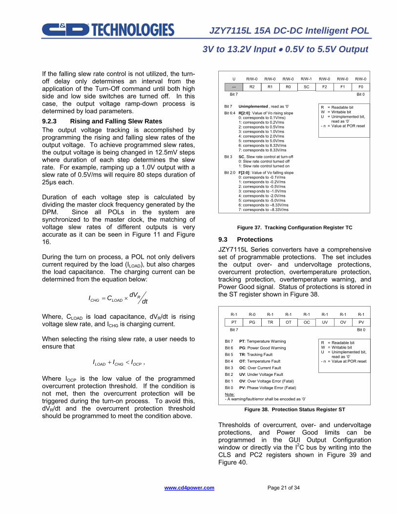
Figure 37. Tracking Configuration Register TC
9.3 Protections JZY7115L Series converters have a comprehensive set of programmable protections. The set includes the output over- and undervoltage protections, overcurrent protection, overtemperature protection, tracking protection, overtemperature warning, and Power Good signal. Status of protections is stored in the ST register shown in Figure 38.
PT PG TR OT UV OV PV
Bit 7 Bit 0
R = Readable bitW = Writable bitU = Unimplemented bit,
read as ‘0’- n = Value at POR reset
R-1 R-0 R-1 R-1 R-1 R-1 R-1R-1
Bit 7 PT: Temperature WarningBit 6 PG: Power Good WarningBit 5 TR: Tracking FaultBit 4 OT: Temperature FaultBit 3 OC: Over Current FaultBit 2 UV: Under Voltage FaultBit 1 OV: Over Voltage Error (Fatal)Bit 0 PV: Phase Voltage Error (Fatal)Note:- A warning/fault/error shall be encoded as ‘0’
OC
Figure 38. Protection Status Register ST
Thresholds of overcurrent, over- and undervoltage protections, and Power Good limits can be programmed in the GUI Output Configuration window or directly via the I2C bus by writing into the CLS and PC2 registers shown in Figure 39 and Figure 40.
--- R2 R1 R0 F2 F1 F0
Bit 7 Bit 0
R = Readable bitW = Writable bitU = Unimplemented bit,
read as ‘0’- n = Value at POR reset
U R/W-0 R/W-0 R/W-0 R/W-0 R/W-0 R/W-0R/W-1
Bit 7 Unimplemented , read as ‘0’
Bit 6:4 R[2:0] : Value of Vo rising slope0: corresponds to 0.1V/ms)1: corresponds to 0.2V/ms2: corresponds to 0.5V/ms3: corresponds to 1.0V/ms4: corresponds to 2.0V/ms5: corresponds to 5.0V/ms6: corresponds to 8.33V/ms7: corresponds to 8.33V/ms
Bit 3 SC, Slew rate control at turn-off0: Slew rate control turned off1: Slew rate control turned on
Bit 2:0 F[2:0]: Value of Vo falling slope0: corresponds to -0.1V/ms1: corresponds to -0.2V/ms2: corresponds to -0.5V/ms3: corresponds to -1.0V/ms4: corresponds to -2.0V/ms5: corresponds to -5.0V/ms6: corresponds to –8.33V/ms7: corresponds to –8.33V/ms
SC
www.cd4power.com Page 22 of 34
JZY7115L 15A DC-DC Intelligent POL
3V to 13.2V Input • 0.5V to 5.5V Output
LR2 LR1 LR0 TCE CLS2 CLS1 CLS0
Bit 7 Bit 0
R = Readable bitW = Writable bitU = Unimplemented bit,
read as ‘0’- n = Value at POR reset
R/W-0 R/W-0 R/W-0 R/W-1 R/W-0 R/W-1 R/W-1R/W-1
Bit 7:5 LR[2:0], Load regulation configuration000: 0 V/A/Ohm001: 0.39 V/A/Ohm010: 0.78 V/A/Ohm011: 1.18 V/A/Ohm100: 1.57 V/A/Ohm101: 1.96 V/A/Ohm110: 2.35 V/A/Ohm111: 2.75 V/A/Ohm
Bit 4 TCE, Temperature compensation enable0: disabled1: enabled
Bit 3:0 CLS[3:0], Current limit setting0h: corresponds to 37%1h: corresponds to 47%…Bh: corresponds to 140%Values higher than Bh are translated to Bh (140%)
CLS3
Figure 39. Current Limit Setpoint Register CLS
--- --- --- PGLL OVPL0 UVPL1 UVPL0
Bit 7 Bit 0
R = Readable bitW = Writable bitU = Unimplemented bit,
read as ‘0’- n = Value at POR reset
U U U R/W-0 R/W-0 R/W-0 R/W-0R/W-1
Bit 7:5 Unimplemented, read as ‘0’Bit 4 PGLL: Set Power Good Low Level
1 = 95% of Vo0 = 90% of Vo (Default)
Bit 3:2 OVPL[1:0]: Set Over Voltage ProtectionLevel00 = 110% of Vo01 = 120% of Vo10 = 130% of Vo (Default)11 = 130% of Vo
Bit 1:0 UVPL[1:0]: Set Under Voltage Protection Level00 = 75% of Vo (Default)01 = 80% of Vo10 = 85% of Vo
OVPL1
Figure 40. Protection Configuration Register PC2
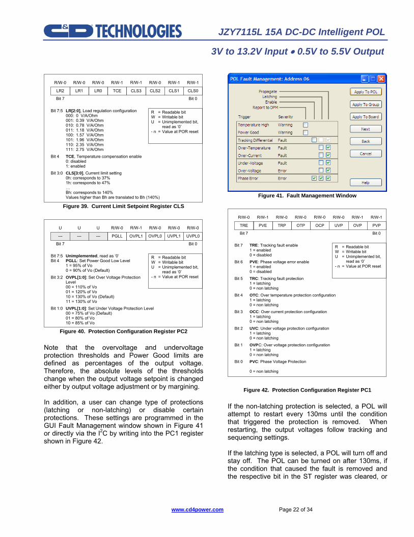
Note that the overvoltage and undervoltage protection thresholds and Power Good limits are defined as percentages of the output voltage. Therefore, the absolute levels of the thresholds change when the output voltage setpoint is changed either by output voltage adjustment or by margining. In addition, a user can change type of protections (latching or non-latching) or disable certain protections. These settings are programmed in the GUI Fault Management window shown in Figure 41 or directly via the I2C by writing into the PC1 register shown in Figure 42.
Figure 41. Fault Management Window
Figure 42. Protection Configuration Register PC1
If the non-latching protection is selected, a POL will attempt to restart every 130ms until the condition that triggered the protection is removed. When restarting, the output voltages follow tracking and sequencing settings. If the latching type is selected, a POL will turn off and stay off. The POL can be turned on after 130ms, if the condition that caused the fault is removed and the respective bit in the ST register was cleared, or
TRE PVE TRP OTP UVP OVP PVP
Bit 7 Bit 0
R = Readable bitW = Writable bitU = Unimplemented bit,
read as ‘0’- n = Value at POR reset
R/W-0 R/W-1 R/W-0 R/W-0 R/W-0 R/W-1 R/W-1R/W-0
Bit 7 TRE: Tracking fault enable1 = enabled0 = disabled
Bit 6 PVE: Phase voltage error enable1 = enabled0 = disabled
Bit 5 TRC: Tracking fault protection1 = latching0 = non latching
Bit 4 OTC: Over temperature protection configuration1 = latching0 = non latching
Bit 3 OCC: Over current protection configuration1 = latching0 = non latching
Bit 2 UVC: Under voltage protection configuration1 = latching0 = non latching
Bit 1 OVPC: Over voltage protection configuration1 = latching0 = non latching
Bit 0 PVC: Phase Voltage Protection
0 = non latching
OCP
www.cd4power.com Page 23 of 34
JZY7115L 15A DC-DC Intelligent POL
3V to 13.2V Input • 0.5V to 5.5V Output
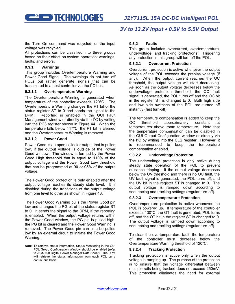
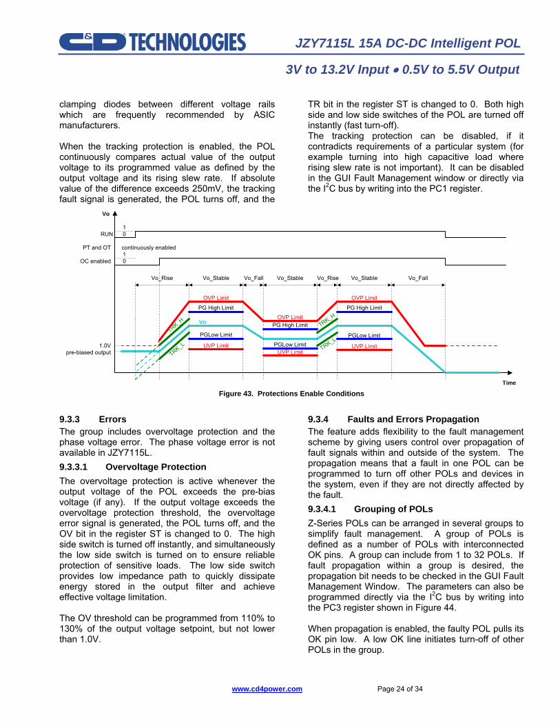
the Turn On command was recycled, or the input voltage was recycled. All protections can be classified into three groups based on their effect on system operation: warnings, faults, and errors. 9.3.1 Warnings This group includes Overtemperature Warning and Power Good Signal. The warnings do not turn off POLs but rather generate signals that can be transmitted to a host controller via the I2C bus. 9.3.1.1 Overtemperature Warning The Overtemperature Warning is generated when temperature of the controller exceeds 120°C. The Overtemperature Warning changes the PT bit of the status register ST to 0 and sends the signal to the DPM. Reporting is enabled in the GUI Fault Management window or directly via the I2C by writing into the PC3 register shown in Figure 44. When the temperature falls below 117°C, the PT bit is cleared and the Overtemperature Warning is removed. 9.3.1.2 Power Good Power Good is an open collector output that is pulled low, if the output voltage is outside of the Power Good window. The window is formed by the Power Good High threshold that is equal to 110% of the output voltage and the Power Good Low threshold that can be programmed at 90 or 95% of the output voltage. The Power Good protection is only enabled after the output voltage reaches its steady state level. It is disabled during the transitions of the output voltage from one level to other as shown in Figure 43. The Power Good Warning pulls the Power Good pin low and changes the PG bit of the status register ST to 0. It sends the signal to the DPM, if the reporting is enabled. When the output voltage returns within the Power Good window, the PG pin is pulled high, the PG bit is cleared and the Power Good Warning is removed. The Power Good pin can also be pulled low by an external circuit to initiate the Power Good Warning. Note: To retrieve status information, Status Monitoring in the GUI
POL Group Configuration Window should be enabled (refer to JZM7100 Digital Power Manager Data Sheet). The DPM will retrieve the status information from each POL on a continuous basis.
9.3.2 Faults This group includes overcurrent, overtemperature, undervoltage, and tracking protections. Triggering any protection in this group will turn off the POL. 9.3.2.1 Overcurrent Protection Overcurrent protection is active whenever the output voltage of the POL exceeds the prebias voltage (if any). When the output current reaches the OC threshold, the output voltage will start decreasing. As soon as the output voltage decreases below the undervoltage protection threshold, the OC fault signal is generated, the POL turns off and the OC bit in the register ST is changed to 0. Both high side and low side switches of the POL are turned off instantly (fast turn-off). The temperature compensation is added to keep the OC threshold approximately constant at temperatures above room temperature. Note that the temperature compensation can be disabled in the GUI Output Configuration window or directly via the I2C by writing into the CLS register. However, it is recommended to keep the temperature compensation enabled. 9.3.2.2 Undervoltage Protection The undervoltage protection is only active during steady state operation of the POL to prevent nuisance tripping. If the output voltage decreases below the UV threshold and there is no OC fault, the UV fault signal is generated, the POL turns off, and the UV bit in the register ST is changed to 0. The output voltage is ramped down according to sequencing and tracking settings (regular turn-off). 9.3.2.3 Overtemperature Protection Overtemperature protection is active whenever the POL is powered up. If temperature of the controller exceeds 130°C, the OT fault is generated, POL turns off, and the OT bit in the register ST is changed to 0. The output voltage is ramped down according to sequencing and tracking settings (regular turn-off). To clear the overtemperature fault, the temperature of the controller must decrease below the Overtemperature Warning threshold of 120°C. 9.3.2.4 Tracking Protection Tracking protection is active only when the output voltage is ramping up. The purpose of the protection is to ensure that the voltage differential between multiple rails being tracked does not exceed 250mV. This protection eliminates the need for external
www.cd4power.com Page 24 of 34
JZY7115L 15A DC-DC Intelligent POL
3V to 13.2V Input • 0.5V to 5.5V Output
clamping diodes between different voltage rails which are frequently recommended by ASIC manufacturers. When the tracking protection is enabled, the POL continuously compares actual value of the output voltage to its programmed value as defined by the output voltage and its rising slew rate. If absolute value of the difference exceeds 250mV, the tracking fault signal is generated, the POL turns off, and the
TR bit in the register ST is changed to 0. Both high side and low side switches of the POL are turned off instantly (fast turn-off). The tracking protection can be disabled, if it contradicts requirements of a particular system (for example turning into high capacitive load where rising slew rate is not important). It can be disabled in the GUI Fault Management window or directly via the I2C bus by writing into the PC1 register.
OVP Limit
PG High Limit
UVP Limit
Vo
Time
Vo
PGLow LimitTRK_H
TRK_L
Vo_Rise Vo_Stable Vo_Fall Vo_Stable Vo_Rise Vo_Stable Vo_Fall
OVP Limit
PG High Limit
UVP Limit
PGLow LimitPGLow Limit
UVP Limit
OVP LimitPG High Limit
1.0V TRK_L
TRK_H
RUN 01
OC enabled 01
pre-biased output
PT and OT continuously enabled
Figure 43. Protections Enable Conditions
9.3.3 Errors The group includes overvoltage protection and the phase voltage error. The phase voltage error is not available in JZY7115L. 9.3.3.1 Overvoltage Protection The overvoltage protection is active whenever the output voltage of the POL exceeds the pre-bias voltage (if any). If the output voltage exceeds the overvoltage protection threshold, the overvoltage error signal is generated, the POL turns off, and the OV bit in the register ST is changed to 0. The high side switch is turned off instantly, and simultaneously the low side switch is turned on to ensure reliable protection of sensitive loads. The low side switch provides low impedance path to quickly dissipate energy stored in the output filter and achieve effective voltage limitation. The OV threshold can be programmed from 110% to 130% of the output voltage setpoint, but not lower than 1.0V.
9.3.4 Faults and Errors Propagation The feature adds flexibility to the fault management scheme by giving users control over propagation of fault signals within and outside of the system. The propagation means that a fault in one POL can be programmed to turn off other POLs and devices in the system, even if they are not directly affected by the fault. 9.3.4.1 Grouping of POLs Z-Series POLs can be arranged in several groups to simplify fault management. A group of POLs is defined as a number of POLs with interconnected OK pins. A group can include from 1 to 32 POLs. If fault propagation within a group is desired, the propagation bit needs to be checked in the GUI Fault Management Window. The parameters can also be programmed directly via the I2C bus by writing into the PC3 register shown in Figure 44. When propagation is enabled, the faulty POL pulls its OK pin low. A low OK line initiates turn-off of other POLs in the group.
www.cd4power.com Page 25 of 34
JZY7115L 15A DC-DC Intelligent POL
3V to 13.2V Input • 0.5V to 5.5V Output
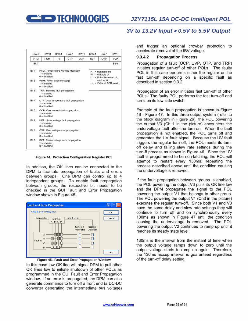
Figure 44. Protection Configuration Register PC3
In addition, the OK lines can be connected to the DPM to facilitate propagation of faults and errors between groups. One DPM can control up to 4 independent groups. To enable fault propagation between groups, the respective bit needs to be checked in the GUI Fault and Error Propagation window shown in Figure 45.
Figure 45. Fault and Error Propagation Window
In this case low OK line will signal DPM to pull other OK lines low to initiate shutdown of other POLs as programmed in the GUI Fault and Error Propagation window. If an error is propagated, the DPM can also generate commands to turn off a front end (a DC-DC converter generating the intermediate bus voltage)
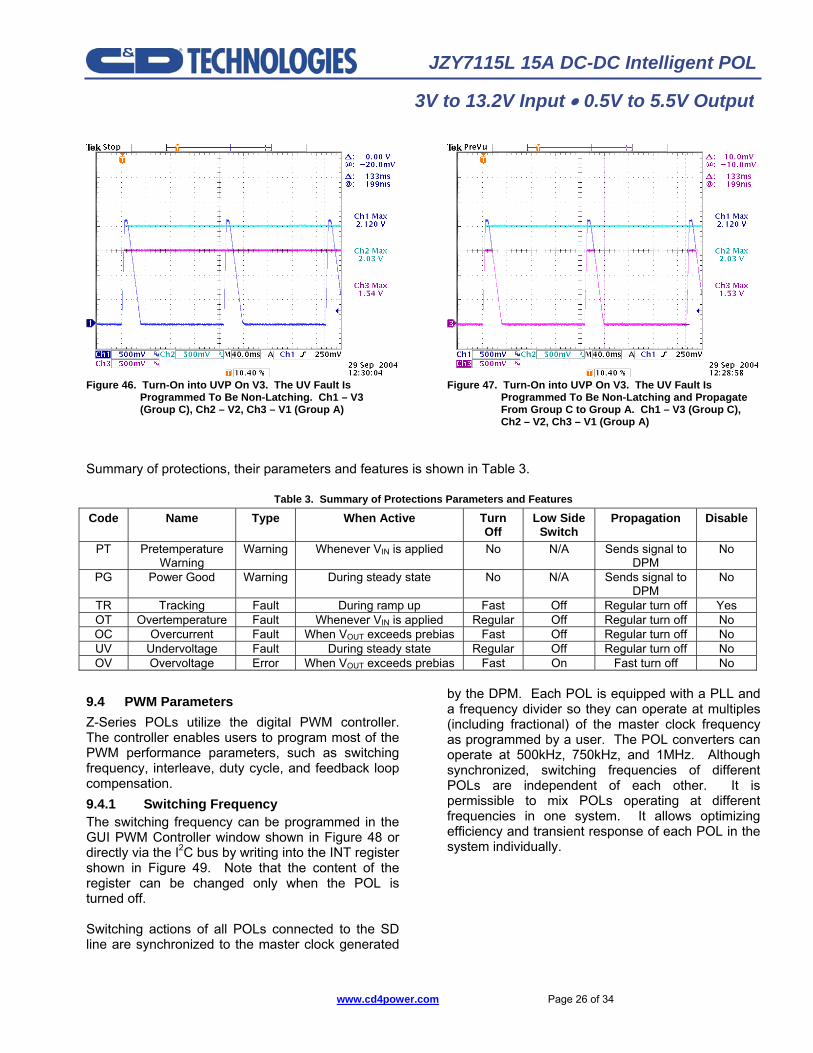
and trigger an optional crowbar protection to accelerate removal of the IBV voltage. 9.3.4.2 Propagation Process Propagation of a fault (OCP, UVP, OTP, and TRP) initiates regular turn-off of other POLs. The faulty POL in this case performs either the regular or the fast turn-off depending on a specific fault as described in section 9.3.2. Propagation of an error initiates fast turn-off of other POLs. The faulty POL performs the fast turn-off and turns on its low side switch. Example of the fault propagation is shown in Figure 46 - Figure 47. In this three-output system (refer to the block diagram in Figure 26), the POL powering the output V3 (Ch 1 in the picture) encounters the undervoltage fault after the turn-on. When the fault propagation is not enabled, the POL turns off and generates the UV fault signal. Because the UV fault triggers the regular turn off, the POL meets its turn-off delay and falling slew rate settings during the turn-ff process as shown in Figure 46. Since the UV fault is programmed to be non-latching, the POL will attempt to restart every 130ms, repeating the process described above until the condition causing the undervoltage is removed. If the fault propagation between groups is enabled, the POL powering the output V3 pulls its OK line low and the DPM propagates the signal to the POL powering the output V1 that belongs to other group. The POL powering the output V1 (Ch3 in the picture) executes the regular turn-off. Since both V1 and V3 have the same delay and slew rate settings they will continue to turn off and on synchronously every 130ms as shown in Figure 47 until the condition causing the undervoltage is removed. The POL powering the output V2 continues to ramp up until it reaches its steady state level. 130ms is the interval from the instant of time when the output voltage ramps down to zero until the output voltage starts to ramp up again. Therefore, the 130ms hiccup interval is guaranteed regardless of the turn-off delay setting.
PTM PGM TRP OTP UVP OVP PVP
Bit 7 Bit 0
R = Readable bitW = Writable bitU = Unimplemented bit,
read as ‘0’- n = Value at POR reset
R/W-0 R/W-0 R/W-1 R/W-1 R/W-1 R/W-1 R/W-1R/W-1
Bit 7 PTM: Temperature warning Message1 = enabled0 = disabled
Bit 6 PGM: Power good message1 = enabled0 = disabled
Bit 5 TRP: Tracking fault propagation1 = enabled0 = disabled
Bit 4 OTP: Over temperature fault propagation1 = enabled0 = disabled
Bit 3 OCP: Over current fault propagation1 = enabled0 = disabled
Bit 2 UVP: Under voltage fault propagation1 = enabled0 = disabled
Bit 1 OVP: Over voltage error propagation1 = enabled0 = disabled
Bit 0 PVP: Phase voltage error propagation1 = enabled0 = disabled
OCP
www.cd4power.com Page 26 of 34
JZY7115L 15A DC-DC Intelligent POL
3V to 13.2V Input • 0.5V to 5.5V Output
Figure 46. Turn-On into UVP On V3. The UV Fault Is
Programmed To Be Non-Latching. Ch1 – V3 (Group C), Ch2 – V2, Ch3 – V1 (Group A)
Figure 47. Turn-On into UVP On V3. The UV Fault Is
Programmed To Be Non-Latching and Propagate From Group C to Group A. Ch1 – V3 (Group C), Ch2 – V2, Ch3 – V1 (Group A)
Summary of protections, their parameters and features is shown in Table 3.
Table 3. Summary of Protections Parameters and Features
Code Name Type When Active Turn Off
Low Side Switch
Propagation Disable
PT Pretemperature Warning
Warning Whenever VIN is applied No N/A Sends signal to DPM
No
PG Power Good Warning During steady state No N/A Sends signal to DPM
No
TR Tracking Fault During ramp up Fast Off Regular turn off Yes OT Overtemperature Fault Whenever VIN is applied Regular Off Regular turn off No OC Overcurrent Fault When VOUT exceeds prebias Fast Off Regular turn off No UV Undervoltage Fault During steady state Regular Off Regular turn off No OV Overvoltage Error When VOUT exceeds prebias Fast On Fast turn off No
9.4 PWM Parameters Z-Series POLs utilize the digital PWM controller. The controller enables users to program most of the PWM performance parameters, such as switching frequency, interleave, duty cycle, and feedback loop compensation. 9.4.1 Switching Frequency The switching frequency can be programmed in the GUI PWM Controller window shown in Figure 48 or directly via the I2C bus by writing into the INT register shown in Figure 49. Note that the content of the register can be changed only when the POL is turned off. Switching actions of all POLs connected to the SD line are synchronized to the master clock generated
by the DPM. Each POL is equipped with a PLL and a frequency divider so they can operate at multiples (including fractional) of the master clock frequency as programmed by a user. The POL converters can operate at 500kHz, 750kHz, and 1MHz. Although synchronized, switching frequencies of different POLs are independent of each other. It is permissible to mix POLs operating at different frequencies in one system. It allows optimizing efficiency and transient response of each POL in the system individually.
www.cd4power.com Page 27 of 34
JZY7115L 15A DC-DC Intelligent POL
3V to 13.2V Input • 0.5V to 5.5V Output
Figure 48. PWM Controller Window
FRQ2 FRQ1 FRQ0 INT4 INT2 INT1 INT0
Bit 7 Bit 0
R = Readable bitW = Writable bitU = Unimplemented bit,
read as ‘0’- n = Value at POR reset
R/W-0 R/W-0 R/W-0 R/W-01) R/W-01) R/W-01) R/W-01)R/W-01)
Bit 7:5 FRQ[2:0]: PWM Frequency Selection000: 500kHz001: 750kHz010: 1000lHz011: 1250kHz100: 1250kHz101: 1500kHz
110: 1750kHz111: 2000kHz
Bit 4:0 INT[4:0]: Interleave position00h: Ton starts with 0.0° Phase lag to SYNQ/DATA Line01h: Ton starts with 11.25° Phase lag to SYNQ/DATA Line02h: Ton starts with 22.50° Phase lag to SYNQ/DATA Line…1Fh: Ton starts with 348.75° Phase lag to SYNQ/DATA Line
1) Initial value depends on the state of the Interleave Mode (IM) Input:IM=Open: At POR reset the 5 corresponding ADDRESS bits are loadedIM=Low: At POR reset a 0 is loaded
INT3
Figure 49. Interleave Configuration Register INT
9.4.2 Interleave Interleave is defined as a phase delay between the synchronizing slope of the master clock on the SD pin and PWM signal of a POL. The interleave can be programmed in the GUI PWM Controller window or directly via the I2C bus by writing into the INT register. Every POL generates switching noise. If no interleave is programmed, all POLs in the system
switch simultaneously and noise reflected to the input source from all POLs is added together as shown in Figure 50.
Figure 50. Input Voltage Noise, No Interleave
Figure 51 shows the input voltage noise of the three-output system with programmed interleave. Instead of all three POLs switching at the same time as in the previous example, the POLs V1, V2, and V3 switch at 0°, 123.75°, and 247.5°, respectively. Noise is spread evenly across the switching cycle resulting in more than 1.5 times reduction. To achieve similar noise reduction without the interleave will require the addition of an external LC filter.
Figure 51. Input Voltage Noise with Interleave
Similar noise reduction can be achieved on the output of POLs connected in parallel. Figure 52 and Figure 53 show the output noise of two JZY7115Ls connected in parallel without and with 180°
www.cd4power.com Page 28 of 34
JZY7115L 15A DC-DC Intelligent POL
3V to 13.2V Input • 0.5V to 5.5V Output
interleave, respectively. Resulting noise reduction is more than 2 times and is equivalent to doubling switching frequency or adding extra capacitance on the output of the POLs.
Figure 52. Output Voltage Noise, Full Load, No Interleave
Figure 53. Output Voltage Noise, Full Load, 180° Interleave
The JZY7115L interleave feature is similar to that of multiphase converters, however, unlike in the case of multiphase converters, interleave does not have to be equal to 360/N, where N is the number of POLs in a system. JZY7115L interleave is independent of the number of POLs in a system and is fully programmable in 11.25° steps. It allows maximum output noise reduction by intelligently spreading switching energy. 9.4.3 Duty Cycle Limit The JZY7115L is a step-down converter therefore VOUT is always less than VIN. The relationship
between the two parameters is characterized by the duty cycle and can be estimated from the following equation:
MININ
OUT
VVDC
.
= ,
Where, DC is the duty cycle, VOUT is the required maximum output voltage (including margining), VIN.MIN is the minimum input voltage. It is good practice to limit the maximum duty cycle of the PWM controller to a somewhat higher value compared to the steady-state duty cycle as expressed by the above equation. This will further protect the output from excessive voltages. The duty cycle limit can be programmed in the GUI PWM Controller window or directly via the I2C bus by writing into the DCL register shown in Figure 54.
DCL5 DCL4 DCL3 DCL2 DCL0 HI LO
Bit 7 Bit 0
R = Readable bit W = Writable bit U = Unimplemented bit, read as ‘0’ - n = Value at POR reset
R/W-1 R/W-1 R/W-1 R/W-0 R/W-0 R/W-0 R/W-0 R/W-1
Bit 7:2 DCL[5:0], Duty Cycle Limitation 00h: 0 01h: 1/64 … 3Fh: 63/64 Bit 1: HI, ADC high saturation feed-forward 0: disabled 1: enabled Bit 0: LO, ADC low saturation feed-forward 0: disabled 1: enabled
DCL1
Figure 54. Duty Cycle Limit Register
9.4.4 ADC Saturation Feedforward To speed up the PWM response in case of heavy dynamic loads, the duty cycle can be forced either to 0 or the duty cycle limit depending on the polarity of the transient. This function is equivalent to having two comparators defining a window around the output voltage setpoint. When an error signal is inside the window, it will produce gradual duty cycle change proportional to the error signal. If the error signal goes outside the window (usually due to large output current steps), the duty cycle will change to its limit in one switching cycle. In most cases this will significantly improve transient response of the controller, reducing amount of required external capacitance. Under certain circumstances, usually when the maximum duty cycle limit significantly exceeds its
www.cd4power.com Page 29 of 34
JZY7115L 15A DC-DC Intelligent POL
3V to 13.2V Input • 0.5V to 5.5V Output
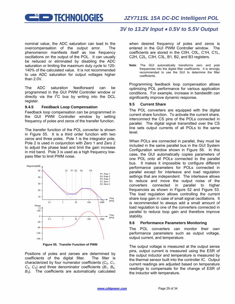
nominal value, the ADC saturation can lead to the overcompensation of the output error. The phenomenon manifests itself as low frequency oscillations on the output of the POL. It can usually be reduced or eliminated by disabling the ADC saturation or limiting the maximum duty cycle to 120-140% of the calculated value. It is not recommended to use ADC saturation for output voltages higher than 2.0V. The ADC saturation feedforward can be programmed in the GUI PWM Controller window or directly via the I2C bus by writing into the DCL register. 9.4.5 Feedback Loop Compensation Feedback loop compensation can be programmed in the GUI PWM Controller window by setting frequency of poles and zeros of the transfer function. The transfer function of the POL converter is shown in Figure 55. It is a third order function with two zeros and three poles. Pole 1 is the integrator pole, Pole 2 is used in conjunction with Zero 1 and Zero 2 to adjust the phase lead and limit the gain increase in mid band. Pole 3 is used as a high frequency low-pass filter to limit PWM noise.
Z1 P1 Z2 P2 P3
0.1 1 10 100 1000
Freq[kHz]
Magnitude[dB]
10
20
30
40
50
0.1 1 10 100 1000
Freq[kHz]
-90
-45
-135
-180
0
+45
Phase[°]
P1: Pole 1P2: Pole 3P3: Pole 3Z1: Zero 1Z2: Zero 2
Figure 55. Transfer Function of PWM
Positions of poles and zeroes are determined by coefficients of the digital filter. The filter is characterized by four numerator coefficients (C0, C1, C2, C3) and three denominator coefficients (B1, B2, B3). The coefficients are automatically calculated
when desired frequency of poles and zeros is entered in the GUI PWM Controller window. The coefficients are stored in the C0H, C0L, C1H, C1L, C2H, C2L, C3H, C3L, B1, B2, and B3 registers. Note: The GUI automatically transforms zero and pole
frequencies into the digital filter coefficients. It is strongly recommended to use the GUI to determine the filter coefficients.
Programming feedback loop compensation allows optimizing POL performance for various application conditions. For example, increase in bandwidth can significantly improve dynamic response.
9.5 Current Share The POL converters are equipped with the digital current share function. To activate the current share, interconnect the CS pins of the POLs connected in parallel. The digital signal transmitted over the CS line sets output currents of all POLs to the same level. When POLs are connected in parallel, they must be included in the same parallel bus in the GUI System Configuration window shown in Figure 56. In this case, the GUI automatically copies parameters of one POL onto all POLs connected to the parallel bus. It makes it impossible to configure different performance parameters for POLs connected in parallel except for interleave and load regulation settings that are independent. The interleave allows to reduce and move the output noise of the converters connected in parallel to higher frequencies as shown in Figure 52 and Figure 53. The load regulation allows controlling the current share loop gain in case of small signal oscillations. It is recommended to always add a small amount of load regulation to one of the converters connected in parallel to reduce loop gain and therefore improve stability.
9.6 Performance Parameters Monitoring The POL converters can monitor their own performance parameters such as output voltage, output current, and temperature. The output voltage is measured at the output sense pins, output current is measured using the ESR of the output inductor and temperature is measured by the thermal sensor built into the controller IC. Output current readings are adjusted based on temperature readings to compensate for the change of ESR of the inductor with temperature.
www.cd4power.com Page 30 of 34
JZY7115L 15A DC-DC Intelligent POL
3V to 13.2V Input • 0.5V to 5.5V Output
An 8-Bit Analog to Digital Converter (ADC) converts the output voltage, output current, and temperature into a digital signal to be transmitted via the serial interface. The ADC allows a minimum sampling frequency of 1kHz for all three values. Monitored parameters are stored in registers (VOM, IOM, and TMP) that are continuously updated. If the
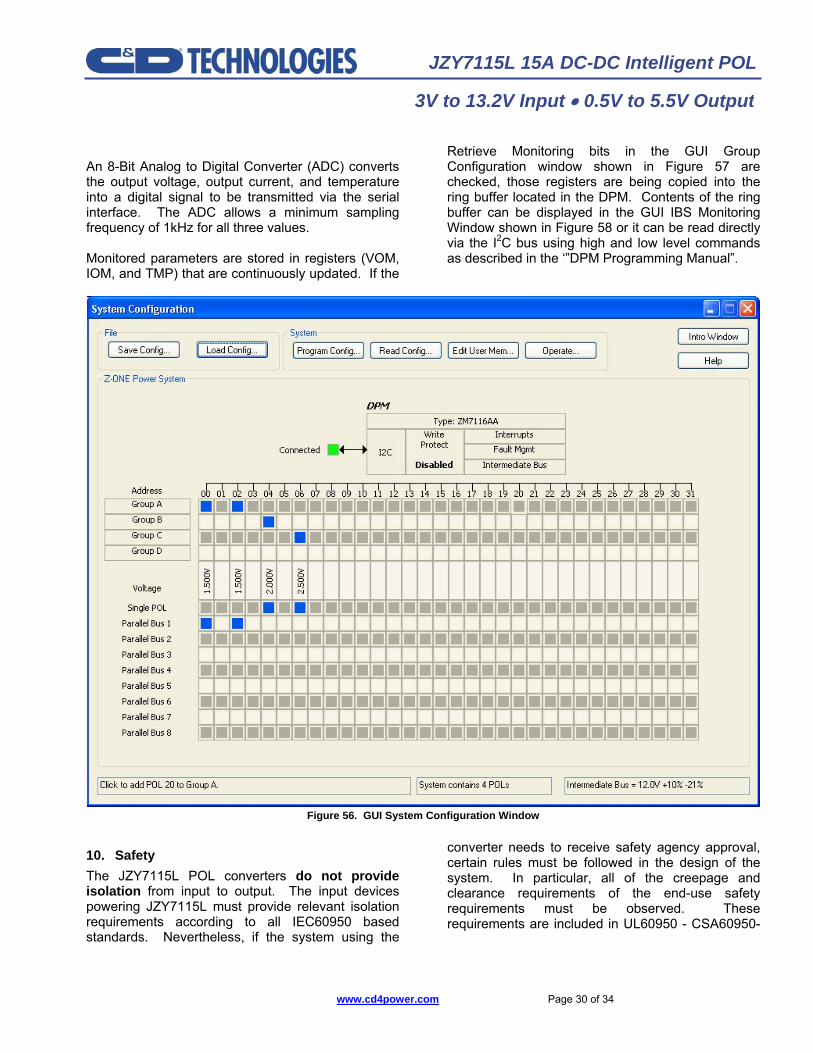
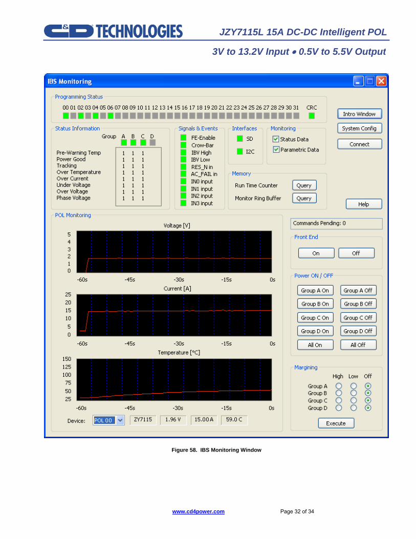
Retrieve Monitoring bits in the GUI Group Configuration window shown in Figure 57 are checked, those registers are being copied into the ring buffer located in the DPM. Contents of the ring buffer can be displayed in the GUI IBS Monitoring Window shown in Figure 58 or it can be read directly via the I2C bus using high and low level commands as described in the ‘”DPM Programming Manual”.
Figure 56. GUI System Configuration Window
10. Safety The JZY7115L POL converters do not provide isolation from input to output. The input devices powering JZY7115L must provide relevant isolation requirements according to all IEC60950 based standards. Nevertheless, if the system using the
converter needs to receive safety agency approval, certain rules must be followed in the design of the system. In particular, all of the creepage and clearance requirements of the end-use safety requirements must be observed. These requirements are included in UL60950 - CSA60950-
www.cd4power.com Page 31 of 34
JZY7115L 15A DC-DC Intelligent POL
3V to 13.2V Input • 0.5V to 5.5V Output
00 and EN60950, although specific applications may have other or additional requirements. The JZY7115L POL converters have no internal fuse. If required, the external fuse needs to be provided to protect the converter from catastrophic failure. Refer to the “Input Fuse Selection for DC/DC converters” application note on <www.cd4power.com> for proper selection of the input fuse. Both input traces and the chassis ground trace (if applicable) must be capable of conducting a current of 1.5 times the value of the fuse without
opening. The fuse must not be placed in the grounded input line. Abnormal and component failure tests were conducted with the POL input protected by a fast-acting 65 V, 15 A, fuse. If a fuse rated greater than 15 A is used, additional testing may be required. In order for the output of the JZY7115L POL converter to be considered as SELV (Safety Extra Low Voltage), according to all IEC60950 based standards, the input to the POL needs to be supplied by an isolated secondary source providing a SELV also.
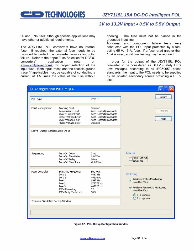
Figure 57. POL Group Configuration Window
www.cd4power.com Page 32 of 34
JZY7115L 15A DC-DC Intelligent POL
3V to 13.2V Input • 0.5V to 5.5V Output
Figure 58. IBS Monitoring Window
www.cd4power.com Page 33 of 34
JZY7115L 15A DC-DC Intelligent POL
3V to 13.2V Input • 0.5V to 5.5V Output
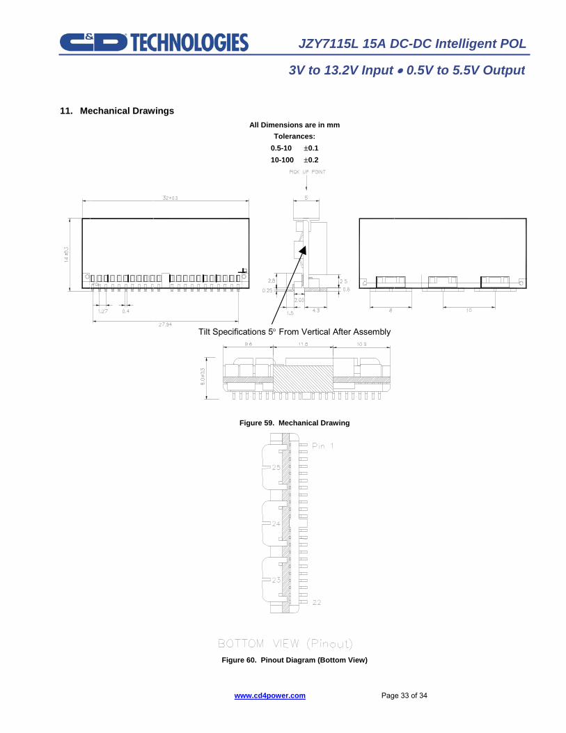
11. Mechanical Drawings All Dimensions are in mm
Tolerances: 0.5-10 ±0.1 10-100 ±0.2
Tilt Specifications 5° From Vertical After Assembly
Figure 59. Mechanical Drawing
Figure 60. Pinout Diagram (Bottom View)
www.cd4power.com Page 34 of 34
JZY7115L 15A DC-DC Intelligent POL
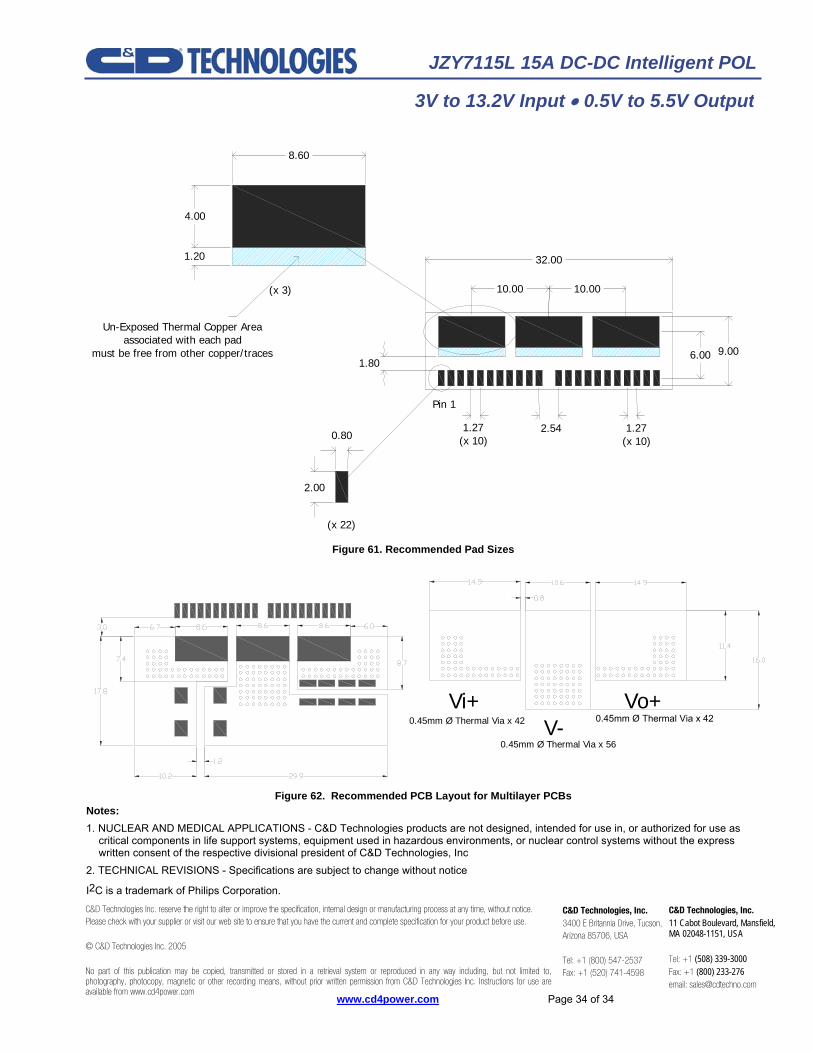
3V to 13.2V Input • 0.5V to 5.5V Output
32.00
10.00
2.00
1.80
0.80
(x 3)
1.27(x 10)
Pin 1
2.54
10.00
4.00
1.20
8.60
9.006.00
1.27(x 10)
Un-Exposed Thermal Copper Areaassociated with each pad
must be free from other copper/traces
(x 22)
Figure 61. Recommended Pad Sizes
0.45mm Ø Thermal Via x 42 0.45mm Ø Thermal Via x 42
0.45mm Ø Thermal Via x 56
Vi+V-
Vo+
Figure 62. Recommended PCB Layout for Multilayer PCBs
Notes: 1. NUCLEAR AND MEDICAL APPLICATIONS - C&D Technologies products are not designed, intended for use in, or authorized for use as
critical components in life support systems, equipment used in hazardous environments, or nuclear control systems without the express written consent of the respective divisional president of C&D Technologies, Inc
2. TECHNICAL REVISIONS - Specifications are subject to change without notice
I2C is a trademark of Philips Corporation. C&D Technologies Inc. reserve the right to alter or improve the specification, internal design or manufacturing process at any time, without notice. Please check with your supplier or visit our web site to ensure that you have the current and complete specification for your product before use. © C&D Technologies Inc. 2005 No part of this publication may be copied, transmitted or stored in a retrieval system or reproduced in any way including, but not limited to,photography, photocopy, magnetic or other recording means, without prior written permission from C&D Technologies Inc. Instructions for use areavailable from www.cd4power.com
C&D Technologies, Inc. 3400 E Britannia Drive, Tucson, Arizona 85706, USA Tel: +1 (800) 547-2537 Fax: +1 (520) 741-4598
C&D Technologies, Inc. 11 Cabot Boulevard, Mansfield, MA 02048-1151, USA Tel: +1 (508) 339-3000 Fax: +1 (800) 233-276 email: [email protected]