junichi taguchi iwai lab. tokyo tech. supervisor: …. the effect of the low temperature long time...
TRANSCRIPT

3. The effect of the low temperature long time anneal for Dy2O3
- 23 -
Master thesis
A study on the effect of the low temperature long time anneal for Dy2O3 and fabrication process of TaN gate electrode
Junichi TAGUCHI
Iwai Lab. Tokyo Tech.
Supervisor: Professor Hiroshi IWAI
Associate Prof. Shun-ichiro OHMI

3. The effect of the low temperature long time anneal for Dy2O3
- 24 -
CCOONNTTEENNTTSS Chapter 1. Introduction………………………………………………………………..1
1.1 Background of this study 1.2 High-k gate insulator 1.3 Issues of processing high-k material
1.3.1 Crystallization during thermal process 1.3.2 Interfacial layer growth 1.3.3 Reduction of carrier mobility in High-k device
1.4 Introduction of TaN gate electrode 1.5 Purpose of this study
Chapter 2. Fabrication and characterization method……………………………….. 11
2.1 Fabrication methods and equipments 2.1.1 Cleaning procedure of Si substrate 2.1.2 MBE system 2.1.3 RTA Rapid Thermal Anneal 2.1.4 Vacuum evaporation system 2.1.5 RF magnetron sputtering system 2.1.6 Mask aligner 2.1.7 RIE Reactive Ion etching
2.2 Characterization method 2.2.1 C-V characteristics
2.2.1.1 Ideal C-V curves 2.2.2 J-V characteristics 2.2.3 AFM Atomic force microscopy 2.2.4 XPS X-ray photoelectron spectroscopy 2.2.5 RHEED 2.2.6 TEM Transmission Electron Microscope 2.2.7 XRD X-ray Diffraction 2.2.8 4 probe method
Chapter 3. The effect of the low temperature long time anneal for Dy2O3………….23 3.1 Physical properties of Dy2O3 3.2 Fabrication Procedure of Al/Dy2O3/n-Si(100) structure 3.3 Investigation on the low temperature long time anneal
3. The effect of the low temperature long time anneal for Dy2O3
- 25 -
3.3.1 Annealing temperature dependence 3.3.2 Annealing time dependence 3.3.3 The effect of chemical oxide preparation
3.4 Summary of this chapter
Chapter 4. Fabrication and characterization of TaN gate electrode…………………39 4.1 Physical properties of TaN 4.2 Experimental procedure 4.3 Characterization of TaN
4.3.1 RF power dependence 4.3.2 N2 ratio dependence 4.3.3 Deposition temperature dependence 4.3.4 Thermal stability of TaN
4.4 Summary of this chapter
Chapter 5. The effect of post metallization anneal with a structure of TaN/Dy2O3/Si(100)…………………………………50
5.1 Fabrication procedure 5.2 Investigation on post metallization anneal 5.3 Summary of this chapter
Chapter 6. Conclusions………………………………………………………………59 6.1 Main results obtained from this study 6.2 Future study
REFERENCE ACKNOWLEDGEMENTS

3. The effect of the low temperature long time anneal for Dy2O3
- 26 -
Chapter 1
Introduction With aggressive scaling of Si-LSI, SiO2 cannot suppress the gate leakage current, due to the oxide thinning. Therefore, SiO2 should be replaced with High-k martial, which shows high dielectric constant. In this chapter, brief overviews of background, and some issues of High-k gate
dielectric were introduced.

3. The effect of the low temperature long time anneal for Dy2O3
- 27 -
1.1 Background of this study Now, information technology is one of the most important technologies in our society. It improves the quality of our society by making social and personal activities more efficient using communication and computer networks. Resent rapid advance in information technology depends on the progress of semiconductor technologies, especially to that of Silicon Large-Scale Integrated Circuits (Si-LSIs). And the progress of Si-LSIs is dependent on down sizing their components such as
metal-oxide-semiconductor field effect transistor (MOSFTEs). The downsizing has been accomplished by the scaling method. In order lateral and
vertical dimensions and supply voltage are scaled down by the factor S, while Si-substrate impurity concentration is increased by the factor S as shown in Figure 1.1 and Table 1.1.
W
Xj L
NA
ND
tox
Substrate
Oxide
MetalW
Xj L
NA
ND
tox
Substrate
Oxide
Metal
Figure 1.1 Schematic structure of a typical MOSFET
Table 1.1 Scaling of MOSFES by a scaling factor of k
1/kk1/k111/k
Device dimension (tox, L, W, xj)Doping concentration (Na, Nd)Voltage (V)Electric field (E)Carrier velocity (v)Capacitance (C = εLW/tox)
Multiple Factor (k>1)MOSFET Device and Circuit Parameters
1/kk1/k111/k
Device dimension (tox, L, W, xj)Doping concentration (Na, Nd)Voltage (V)Electric field (E)Carrier velocity (v)Capacitance (C = εLW/tox)
Multiple Factor (k>1)MOSFET Device and Circuit Parameters

3. The effect of the low temperature long time anneal for Dy2O3
- 28 -
Since early sixties, (C)MOS device has relied on SiO2 as the gate insulator. Further size reduction and the ever demanding technology roadmaps have imposed scaling constraints on gate insulator thickness to the point where excessive tunneling currents make transistor design untenable. The leakage current of 1nm-thick SiO2 is 100A/cm2, therefore, power consumption becomes very huge. In order to suppress the huge leakage current below 1 nm regime, the replacement of SiO2 with a high dielectric constant material which allows an increase in the physical oxide thickness maintaining a low equivalent oxide thickness (EOT) and low gate leakage current is necessary as shown in Table 1.2. Therefore, the replacement SiO2 with High-k is promising to thick the film, keeping EOT as shown in Figure 1.2.
e-e-e-e- e-e-
e-e-
e-e-e-e-
e-e-
SiO2
e-e-e-e-
e-e-
e-e-
tSi thigh-k = αtSi
εr = 3.9
εr = 3.9α
Poly-Si n-Si High-kPoly-Si n-Si
e-e-
Figure 1.2 Reduction of leakage current by replacement SiO2 with High-k material. High-k material, which shows α times dielectric constant as much as SiO2, allow to α
times thickness with keeping the capacitance of insulator as following equation Teq = εsi/tsi = εHigh-k/tHigh-k
Table 1.2 ITRS for high performance logic
0.4 – 0.60.8 - 1.31.3 - 1.6Teq (nm)
183265LG (nm)
201320052001Year
0.4 – 0.60.8 - 1.31.3 - 1.6Teq (nm)
183265LG (nm)
201320052001Year
High-performance Logic Technology Requirements
3. The effect of the low temperature long time anneal for Dy2O3
- 29 -
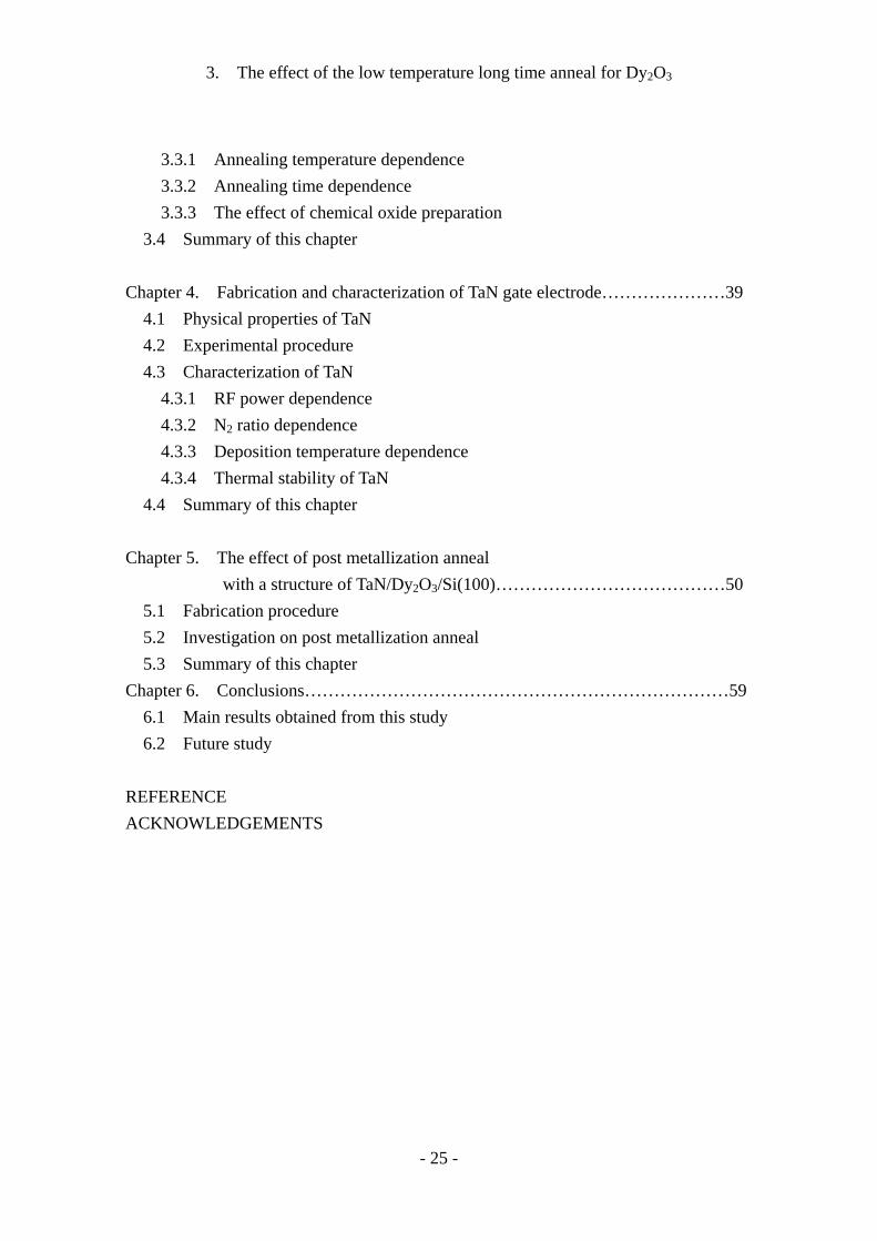
1.2 High-k gate insulator Requirements to candidate dielectrics are: 1. a high dielectric constant k 2. stable in contact with silicon substrate at high temperature 3. a low density of defects in bulk (Qtot < 5x1010 cm-2) and at the interface (Dit <
5x1010 cm-2) 4. high offset barriers of 1 eV for both electrons and holes Metal oxides (MOx) are promising candidates for the High-k gate material. Important
properties needed for those metal oxides are: 1. no-radioactivity, 2. being solid at the temperature of LSI process 3. chemical stability at Si interface. Table 1.3 shows candidates for the metal oxides that are thought to satisfy the above conditions (1-3) Recently, many High-k materials such as Al2O3, ZrO2, HfO2, La2O3 or thereof
(silicates, aluminates) have been investigated as gate insulator (shown in Figure 1.3) and promising results were obtained for the characteristics of J-EOT as shown in Figure. 1.4.
Table 1.3 Candidates for metal, oxide of which has possibility to be used as High-k gate insulator on periodic table
H
Li Be
Mg
Ca Sc V Cr Mn Fc Co Ni Cu Zn Ga Ge As Se Br Kr
Na
K
Rh Sr Y Zr Nb Mo Tc Ru Rb Pd Ag Cd In Sn Sb Te I Xe
Cs Ba Hf Ta W Re Os Ir Pt Au Hg Tl Pb Bi Po At Rn
B C N O F Ne
He
Al Si P S Cl Ar
Fr Ra Rf Ha Sg Ns Hs Mt
La Ce Pr Nd Pm Sm Eu Gd Tb Dy Ho Er Tm Yb Lu
Ac Th Pa U Np Pu Am Cm Bk Cf Es Fm Md No Lr
‡
†
‡
†
React with Si. Other failed reactions.Reported since Dec. 1999.(MRS, IEDM, ECS, VLSI)
Ti

3. The effect of the low temperature long time anneal for Dy2O3
- 30 -
VLSI 2001 IEDM2001 IWGI2001 VLSI 2002
SiNLanthanoidePr2O3Ta2O5La2O3
AlTiOAlONAlNAl2O3ZrAlOZrONZr-silicateZrO2HfSiON
HfONHfAlOHf-SilicateHfO2
10
20
Num
ber
of p
ublis
hed
pape
r
VLSI 2001 IEDM2001 IWGI2001 VLSI 2002
SiNLanthanoidePr2O3Ta2O5La2O3
AlTiOAlONAlNAl2O3ZrAlOZrONZr-silicateZrO2HfSiON
HfONHfAlOHf-SilicateHfO2
10
20
Num
ber
of p
ublis
hed
pape
r
Figure 1.3 Reported materials as High-k gate insulator
on VLSI symp., IEDM and IWGI
10-10
10-6
10-2
102
0.5 1.0 1.5
HfO2NH3+HfO2HfSiONZrO2Zr-SilicateAl2O3NH3+ZrO2Zr-Al-Si-OPr2O3Nd2O3Sm2O3Gd2O3Lu2O3Dy2O3La2O3SiO2Nitrided SiO2
EOT (nm)
Curr
ent
Den
sity
(A/
cm2 )
Figure 1.4 Current density – EOT characteristics for various High-k material

3. The effect of the low temperature long time anneal for Dy2O3
- 31 -
1.3 Issues of processing High-k material However, one should realize there are still a number of problems to be solved. A brief overview of some these issues were given. 1.3.1 Crystallization during thermal process During subsequent processing, High-k thin film must withstand thermal anneals at high temperatures up to 1000oC during which they should not re-crystallize. Single oxide layers of ZrO2 and HfO2 are known to re-crystallize at fairly low temperatures (400 – 600 oC), depending on layer thickness. These crystallization causes leakage current and issues of reliabilities. To overcome this problem, silicate or aluminate of these oxides have been studied recently. Mixtures of HfO2 or ZrO2 with Al2O3 are found to re-crystallize only at much high temperature, up to 1000 oC. 1.3.2 Interfacial layer growth Secondly, there is a issue of interfacial layer growth. The interfacial layer (SiOx, silicate) that shows a low dielectric constant lower the effective dielectric constant of total insulator stacks. As shown figure 1.5, ZrO2 tends to react with Si substrate. To overcome this problem, surface treatment (oxidized, nitrided) was known to be effective to suppress the interfacial reaction between Si and High-k materials.
Figure 1.5 interfacial layer growth and micro crystallization

3. The effect of the low temperature long time anneal for Dy2O3
- 32 -
1.3.3 Reduction of carrier mobility in High-k devices C-V and J-V characteristics on High-k capacitors are used to show the promising results of those new materials for gate insulator. However, recent result of mobility on MOSFET have indicated that electron and hole mobility underneath High-k layers is quite often strongly reduces as compared to SiO2. A summary of recent data published at IEDM 2001 (Figure 1.6) indicates that this mobility is strongly influenced by the presence and characteristics of an interfacial layer, either SiO2 or silicate-like. This mobility reduction is said to be due to phonon scattering. This could become a showstopper in view of the final aim of very low EOT values.
100
200
300
400
00 0.5 1.0 1.5
Max
imum
ele
ctro
n m
obili
ty(c
m2 V
-1s-1
)
Interfacial oxide thickness (nm)
100
200
300
400
00 0.5 1.0 1.5
Max
imum
ele
ctro
n m
obili
ty(c
m2 V
-1s-1
)
Interfacial oxide thickness (nm) Figure 1.6 Electron mobility for various High-k material
1.4 Introduction of TaN gate electrode In order to suppress the interfacial layer growth, the films were annealed after the gate metal deposition. Therefore, it is necessary to investigate on the metal electrode, which shows high thermal stability. In this study, TaN was investigated as gate electrode. This material is now researched at institutes all over the world in order to solve Poly-depletion effect. As CMOS devices are scaled into sub-0.1 µm regime that High-k material is necessary
for gate insulator, poly-depletion effects become a significant concern. They increase the effective oxide thickness, degrade the device performance, and make further gate

3. The effect of the low temperature long time anneal for Dy2O3
- 33 -
oxide scaling problematic.(Figures. 1.7, 1.8) Therefore, metal gate electrodes are being explored to replace the Poly-Silicon gate to
minimize the poly-depletion effects in addition to reduction of gate –line sheet resistance. The metal gates must have suitable work function and required thermal and chemical stability with underlying thin gate insulator for CMOS processing. Several materials have been studied as a replacement for poly-Si, such as TiN, Mo, Ta, TaN etc.
poly-Si High-k n-Si Metal High-k n-Sipoly-Si High-k n-Sipoly-Si High-k n-Si Metal High-k n-SiMetal High-k n-Si
Figure 1.7 Schematic diagram of Poly-depletion effect

3. The effect of the low temperature long time anneal for Dy2O3
- 34 -
In this study, TaN is studied for gate electrode with thermal stability. Some excellent
results were reported such as high thermal stability and interface properties during for TaN gate electrode at IEDM 2001 (Figure 1.9). These reports indicate TaN is promising material as gate electrode with thermally stable.
Figure 1.8 Acceleration of poly-depletion effect due to oxide thining

3. The effect of the low temperature long time anneal for Dy2O3
- 35 -
Figure 1.9 Excellent thermal stability for TaN/SiO2 structure 1.5 Purpose of this study Several High-k material such as HfO2 and ZrO2 have been studied and show excellent result. However, they are not the complete solution for High-k gate material because of some issues mentioned above. In this study, amorphous Dy2O3, which is one of the rare earth oxides, is studied for gate insulator application. Dy2O3 MIS capacitor has few reports and characteristics aren’t well known. So, the purpose of this study is to investigate fundamental characteristics of Dy2O3 thin film, and improve the film quality with out crystallization and interfacial layer growth And in order to research the annealing effect after the metal deposition, the fabrication process of TaN electrode was researched for thermally stable gate metal.

3. The effect of the low temperature long time anneal for Dy2O3
- 36 -
Chapter 2
Fabrication and characterization methods In this chapter, the fabrication and characterization methods of MIS diode were introduced briefly.

3. The effect of the low temperature long time anneal for Dy2O3
- 37 -
2.1 Fabrication methods and equipments 2.1.1 Cleaning procedure of Si substrate Prior to use a bare Si substrate, it should be chemically cleaned to remove the particles as well as any traces of organic, ionic and metallic impurities from the surface. The procedure of cleaning of substrate in this study is shown in Table 2.1.
Table 2.1 Substrate cleaning procedure
Oxide layer4. Immerse in (1:100) solution of HF-H2O for 60 sec
Organic, metal contamination
1. Wash in DI water for 10 min2. Immerse in (4:1) solution of H2SO4-H2O2 (SPM) for 5 min3. Wash in DI water for 10 min
Removal objectCleaning procedure
Oxide layer4. Immerse in (1:100) solution of HF-H2O for 60 sec
Organic, metal contamination
1. Wash in DI water for 10 min2. Immerse in (4:1) solution of H2SO4-H2O2 (SPM) for 5 min3. Wash in DI water for 10 min
Removal objectCleaning procedure
2.1.2 MBE system Electron Beam Evaporation (EBE) method using MBD equipment is employed for depositing Dy2O3 in this study.
Figure 2.1 shows the schematic drawings of the equipment and inside of its growth chamber. Air in the loading chamber is removed to degree of a vacuum of 10-8 Torr by a turbo molecular pump connected to a rotary pump. Vacuum in the growth chamber reaches as high as 10-10 Torr by the removal of air with an ion pump and the introduction of liquid N2 trap.
In the growth chamber, sintered Dy2O3 target, which is evaporation source, is irradiated with electron beam accelerated by -5 kV. The target is heated up and Dy2O3 molecules are evaporated. Then ultra thin Dy2O3 film is deposited on the Si-substrate. The degree of a vacuum is around 10-7 Torr while deposition. The substrate rotates 10 times per 1 minute horizontally to uniform the film thickness. Physical thickness of the film is monitored with a film thickness counter using crystal oscillator. The temperature of the substrate is controlled by a substrate heater and is measured by a thermocouple. The significant features of this method are as follows:
1. Because the film is evaporated by using its own constituent as a raw material, contaminants, e.g. carbon, chloride, included in this method are much less than those in CVD (Chemical Vapor Deposition) which use precursor. 2. Damages caused by the depositing of this method are much less than those of sputtering.

3. The effect of the low temperature long time anneal for Dy2O3
- 38 -
Electron Beam Gun
Heater
Loading Chamber
Ion Pump TMP
RP
Ultra High Vacuum Chamber
Dy2O3
Figure 2.1 MBE system
2.1.3 RTA Rapid Thermal Anneal RTA (Rapid Thermal Anneal) equipment (MILA-3000, ULVAC Co. Ltd.) was used for annealing sample of before/after metal gate deposition. The schematic diagram is shown in Figure 2.2. The temperature was controlled by PID controller. Before the anneal, the ambient of the furnace was replaced with O2 or N2 gas. The rate of temperature increase was set to 400 oC/min in this study.
O2 N2
Suscepter Sample
infrared heaterquartz reactor core.
Figure 2.2 RTA equipment 2.1.4 Vacuum evaporation system Top and bottom electrodes of Al were deposited by a vacuum evaporation equipment with a bell jar shown in Figure 2.3. In a vacuum of approximately 10-5 Torr, Al is

3. The effect of the low temperature long time anneal for Dy2O3
- 39 -
evaporated with resistance heating of W filament and Al film is deposited on samples.
W Filament
Al wire
Sample
Figure 2.3 Vacuum evaporation of Al 2.1.5 RF magnetron sputtering system TaN gate electrode was deposited by RF magnetron sputtering system (JEC-SP360R), schematic diagram of which was shown in Figure 2.4. This equipment deposits metal films by means of physical sputtering that occurs in a magnetically-confined RF plasma discharge of an inert Ar gas. Before the introduction of gases (Ar, Kr, N2 or O2), the process chamber was evacuated to degree of 10-5 Pa by a turbo molecular pump connected to a rotary pump and a liquid N2 trap. The flow rate of gases is controlled by mass flow. The RF power supply system has auto impedance matching equipment and its capability of power supply is ~ 500W. In the process chamber, there is a substrate heater, which can heat samples from RT to 800 oC

3. The effect of the low temperature long time anneal for Dy2O3
- 40 -
ArN2
Substrate Heater Sample
Ta Target
Top electrode
RF Power Source
Plasma
Figure 2.4 RF magnetron sputtering system
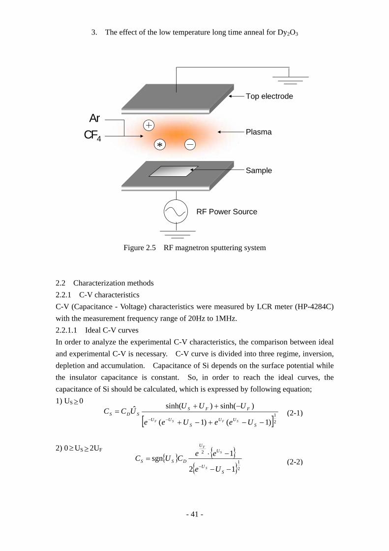
2.1.6 Mask aligner The spin-coated photoresist was exposed through the mask with high-intensity ultraviolet light (405 nm). In this study, the exposure process was performed by contact-type mask aligner, MJB3 (Karl Suss Co. Ltd.). The exposure time was set to 12 sec. The photoresist was developed using the specified developer (MND-3, Tokyo Ohka Co. Ltd.). 2.1.7 RIE Reactive Ion Etching RIE system was employed for etching TaN gate electrode. RIE combined the plasma and sputter etching process. Plasma systems are used to ionize reactive gases, and the ions are accelerated to bombard the surface. Etching process occurs though a combination of chemical reaction and momentum transfer from the etching species.
3. The effect of the low temperature long time anneal for Dy2O3
- 41 -
*
RF Power Source
Top electrode
ArCF4
Sample
Plasma
Figure 2.5 RF magnetron sputtering system
2.2 Characterization methods 2.2.1 C-V characteristics C-V (Capacitance - Voltage) characteristics were measured by LCR meter (HP-4284C) with the measurement frequency range of 20Hz to 1MHz. 2.2.1.1 Ideal C-V curves In order to analyze the experimental C-V characteristics, the comparison between ideal and experimental C-V is necessary. C-V curve is divided into three regime, inversion, depletion and accumulation. Capacitance of Si depends on the surface potential while the insulator capacitance is constant. So, in order to reach the ideal curves, the capacitance of Si should be calculated, which is expressed by following equation; 1) US≥0 2) 0≥US≥2UF
[ ]21
)1()1(
)sinh()sinh(ˆ
−−+−+
−++=
−−S
UUS
UU
FFSSDS
UeeUee
UUUUCC
SFSF
2
1
2
12
1sgn−−
−⋅=
−S
U
UU
DSS
Ue
eeCUCS
S
F
(2-1)
(2-2)

3. The effect of the low temperature long time anneal for Dy2O3
- 42 -
3) 2UF≥US
U(x) and Us in above equation is follow,
kT
xqxU )()( φ≡
kTq
U SS
φ≡
and the capacitance of MIS diode can be calculated as formula (2-5),
si
si
CCCC
C+
= (2-5)
2.2.2 J-V characteristics J-V (leakage Current – Voltage) characteristics were measured by semiconductor parameter analyzer (HP4284C, Agilent Technologies). 2.2.3 AFM Atomic Force Microscopy The roughness of the surface of the film is evaluated by Atomic Force Microscope (AFM, Nano Scope III, Digital Instrument Co. Ltd.) in tapping mode. AFM is a microscopic equipment for observing surface of a sample with high
magnification. Figure 2.6 shows the principle of AFM. As the sample approaches the probe of AFM slowly and the distance between them becomes a certain value, attractive or repulsive force is generated between them. A cantilever to which the probe is attached distorts because of the force. The distortion is detected by a variation of reflection angle of laser beam which is irradiated to the cantilever. The distance is controlled to keep the distortion constant while scanning the surface of the sample with the probe. An image of the surface is obtained by the scanning in x and y directions and the control of the distance in z direction. Spatial resolution of AFM used in this study is around 1.0 nm.
[ ] [ ] 21
1)exp()exp(1)exp()exp(, −−+−+−−≡ SSFSSFFS UUUUUUUUF
∫ −==
SU
F
xU
D
m
SS
UxUFxdUe
CW
C
0
)(
),()()1(
ε
(2-3)
(2-4)

3. The effect of the low temperature long time anneal for Dy2O3
- 43 -
Figure 2.6 Atomic Force Microscopy
2.2.4 XPS X-ray photoelectron spectroscopy Photoelectron spectroscopy is based upon a single photon in/electron out process and from many viewpoints this underlying process is a much simpler phenomenon than the Auger process. The energy of a photon is given by the Einstein relation:
hvE = (2.6) where h -Plank’s constant (6.62x10⁻³⁴ Js), v -frequency (Hz) of the radiation. In XPS the photon is absorbed by an atom in a molecule or solid, leading to ionization and the emission of a core (inner shell) electron. The kinetic energy distribution of the emitted photoelectrons can be measured using any appropriate electron energy analyzer and a photoelectron spectrum can thus be recorded. The process of photo ionization can be considered in following equation:
−+ +→+ eAhvA (2.7) Conservation of energy then requires that:
)()()( −+ +=+ eEAEhvAE (2.8) Since the electron’s energy is present solely as kinetic energy (KE), this can be
rearranged to give the following expression for the KE of the photoelectron: )]()([ AEAEhvKE −−= + (2.9)
The final term in brackets, representing the different in energy between the ionized and neutral atoms, is generally called the binding energy (BE) of the electron – this then leads to the following commonly quoted equation:

3. The effect of the low temperature long time anneal for Dy2O3
- 44 -
BEhvKE −= (2.10) For each element, there is a characteristic binding energy associated with each core
atomic orbital i.e. the presence of peaks at particular energies therefore indicates the presence of a specific element in the sample. Furthermore, the intensity of the peaks is related to the concentrations of the element. Thus, the technique is capable of yielding a quantitative analysis. And the binding energy depends not only on the level from photoemission is occurring, but also on the formal oxidation state of the atom and the local chemical and physical environment. They give rise to small shifts in peak positions in the spectrum. From the peak shifts, the binding condition of the elements was obtained.
hν
Core Level
Vacuum Level KE
BEhν
Figure 2.7 Schematic diagram of photo emission by X-ray
45o
e-X-ray
detector
Figure 2.8 Schematic diagram of XPS System 2.2.5 RHEED Reflection High Energy Electron Diffraction or RHEED is a surface sensitive technique which allows to qualitatively measure properties of the surface of a sample. This technique can also be carried out quantitatively to measure the in-plane surface lattice parameters and the in-plane coherence length of a sample. In RHEED an electron beam has an incident angle of about one degree. Due to the

3. The effect of the low temperature long time anneal for Dy2O3
- 45 -
strong interaction of the electron beam and the electronic system of the sample the penetration depth is limited to a few Å.
e-gun
screenSubstrate
Figure 2.9 Principle of RHEED 2.2.6 TEM Transmission Electron Microscope TEM (Transmission Electron Microscope) was used for observing cross sectional images of high-k/Si substrate interface in this study. The electron high-energy beam of the order of 100 keV passes through the sample of
less than 10 nm thickness. From transmitted electrons, a diffraction pattern or a high resolution image in atomic level can be obtained.

3. The effect of the low temperature long time anneal for Dy2O3
- 46 -
Electron gun
Focus lens
Objective lens
Projective lens
Image
Sample
Figure 2.10 Principle of RHEED 2.2.7 XRD X-ray diffraction Film crystallization was characterized by XRD. In principle XRD measurements come down to measuring distances between planes with plane x-ray waves (wavelength of a few tenths of a nm). When 2d equals nλ = 2d sinθ, the Bragg condition nλ = 2d sinθ is satisfied and a peak can be measured.
θ θ
d=plane distance
X-ray
Incoming beam Reflected beam
Figure 2.11 Principle of XRD

3. The effect of the low temperature long time anneal for Dy2O3
- 47 -
2.2.8 4 probe method The resistivity of metal electrode was evaluated by 4 prove method. The schematic diagram was shown in Figure 2.12. A small current (I) is passed though two outer probes and voltage (V) is measured between the two inner probes. If the spacing between the probes is much greater than the film thickness but much smaller than the size of the conducting film, the resistance of the film can be obtained from following equation:
)(2ln I
Vtπρ = (2.10)
where t -film thickness, V -outer probe voltage, I -inner probe current.
AV
Sampled d d
Figure 2.12 4 prove method

3. The effect of the low temperature long time anneal for Dy2O3
- 48 -
Chapter 3
The effect of the low temperature long time anneal for Dy2O3
In this chapter, fundamental electrical characteristics of MOS capacitors with a Al/Dy2O3/n-Si (100) structure were evaluated in advance. And the effects of the low temperature long time anneal and substrate preparation by H2O2 before the deposition

3. The effect of the low temperature long time anneal for Dy2O3
- 49 -
were researched. 3.1 Physical properties of Dy2O3 Dy is one of the rare earth elements, atomic number of which is 66. From its location in the periodic table, Dy belongs to heavy rare earth group. In this study, its oxide, Dy2O3 thin film was fabricated and evaluated. Dy2O3 was deposited as amorphous thin film. However, it was crystallize in the case
of the deposition on high temperature substrate. Its crystal systems are shown in Figure 3.1 and lattice constant of Dy2O3 is shown in Table 3.1. Dy2O3 takes two types of crystal system, B type – monoclinic and C type – cubic. In
the normal pressure, C-type structure is stable at various temperatures. On the other hand, B-type structure is stable in the high pressure. C-type crystal transit the phase into B type in the condition of 3.5x10⁴ atm, 1000 oC, and i.e. the density of these phase are ρB > ρC. And the transited phase on the high pressure condition re-transits to C type in a few hour in the normal pressure.
(B type) (C type)(B type) (C type)Figure 3.1 Crystal structure of Dy2O3 From top to bottom, B type and C type. Black
point and small circles represents Dy and O, respectively.

3. The effect of the low temperature long time anneal for Dy2O3
- 50 -
Table 3.1 Lattice constant of Dy2O3
100.000.86610.35191.397Monoclinic(B type)
-1.0667Cubic(C type)
Structure system a (nm) b (nm) β (degree)c (nm)
100.000.86610.35191.397Monoclinic(B type)
-1.0667Cubic(C type)
Structure system a (nm) b (nm) β (degree)c (nm)
Table 3.2 shows the physical properties of various High-k materials. As to contact
stability, Dy2O3 shows higher Gibbs free energy for the Si than the other High-k candidates listed in Table 3.2. As compared with the others, the suppression of the interfacial layer is expected for Dy2O3. With regard to bandgap, it is known as 4.8 eV, which is slightly less than the others, and dielectric constant is 12 – 18, which is almost the average value among the lanthanide oxide series.
Table 3.2 Physical properties for various High-k materials
4.85.2 – 7.85.75.48.88 – 9Bandgap (eV)
112.442.347.698.563.4StableConstant stability with Si(kJ/mol) Si+MOx M+SiO2
-13514-11188-12452-15926-13125Lattice energy (kJ/mol)
Effective κ value 3.9
SiO2
8.5 – 10
Al2O3
~24
HfO2
27
La2O3
12 – 1811 – 18.5
Dy2O3ZrO2
4.85.2 – 7.85.75.48.88 – 9Bandgap (eV)
112.442.347.698.563.4StableConstant stability with Si(kJ/mol) Si+MOx M+SiO2
-13514-11188-12452-15926-13125Lattice energy (kJ/mol)
Effective κ value 3.9
SiO2
8.5 – 10
Al2O3
~24
HfO2
27
La2O3
12 – 1811 – 18.5
Dy2O3ZrO2
3.2 Fabrication procedure of Al/Dy2O3/n-Si(100) structures Fabrication process of MIS capacitor is shown in Figure 3.2. Dy2O3 films were deposited by electron beam evaporation in ultra high vacuum (UHV) chamber at room temperature or 250oC on n-type Si(100) substrates treated by diluted HF (HF-last). Some of the samples were chemically oxidized by H2O2 dip to form 0.5nm SiO2 layer

3. The effect of the low temperature long time anneal for Dy2O3
- 51 -
before the deposition of Dy2O3 films (Chemical Oxide). MBE system is used to deposit Dy2O3 thin film. The deposition rate of the film was about 0.7nm/min. The deposited samples were then annealed at 200oC - 1000oC for 5 - 90min in O2 or N2 ambient. Al electrode was deposited on the top of the oxide and Al back electrode was deposited on backside of n-Si (100) substrate. These MIS (Al/High-k/n-Si/Al) capacitors were characterized by C-V, J-V, AFM and XPS.
Dy2O3 Deposition (Tsub=R.T. or 250oC)
Substrate Cleaning (SPM & HF dip)
Al Back Electrode deposition
Chemical Oxide preparation(H2O2 30min)
RTA (O2 or N2)
Al Top Electrode deposition
Figure 3.2 Fabrication procedure of MIS diode
3.3 Investigation on the low temperature long time anneal for Dy2O3 3.3.1 Annealing temperature dependence Figures 3.3 – 3.6 show C-V characteristics of MIS capacitors for the HF last samples. The measurement frequency was 100 kHz. The film deposition temperature was room temperature or 250 oC, and the physical thickness of these films was about 5.5 nm for each temperature. The annealing temperature was 200oC – 1000oC. Annealing over 200oC, the hysteresis loop disappeared and the leakage current densities decreased (shown in Figures 3.7, 3.8). As annealing at higher temperature, the accumulation

3. The effect of the low temperature long time anneal for Dy2O3
- 52 -
capacitances decreased because of the formation of the interfacial layer growth.
0
1
2
3
-1 0 1
Capa
cita
nce
(µF/
cm2 )
Voltage (V)
Al/Dy2O
3/ n-Si(100)/Al
R.T. depo @100kHzasdepo
200oC400oC
600oC800oC
1000oC
Figure 3.3 C-V characteristics for O2 5min annealed samples deposited at RT
0
1
2
3
-1 0 1
Capa
cita
nce
(µF/
cm2 )
Voltage (V)
Al/Dy2O
3/ n-Si(100)/Al
250oC depo @100kHz asdepo
200oC
400oC
600oC
800oC
1000oC

3. The effect of the low temperature long time anneal for Dy2O3
- 53 -
Figure 3.4 C-V characteristics for O2 5min annealed samples deposited at 250 oC
0
1
2
3
-1 0 1
Capa
cita
nce
(µF/
cm2 )
Voltage (V)
Al/Dy2O
3/ n-Si(100)/Al
R.T. depo @100kHzasdepo
200oC
400oC
600oC
800oC
1000oC
Figure 3.5 C-V characteristics for N2 5min annealed samples deposited at RT
0
1
2
3
-1 0 1
Capa
cita
nce
(µF/
cm2 )
Voltage (V)
Al/Dy2O
3/ n-Si(100)/Al
250oC depo @100kHzasdepo
200oC
400oC
600oC
800oC
1000oC

3. The effect of the low temperature long time anneal for Dy2O3
- 54 -
Figure 3.6 C-V characteristics for N2 5min annealed samples deposited at 250 oC
10-10
10-8
10-6
10-4
10-2
100
0 0.5 1 1.5 2
Curr
ent
Den
sity
(A/
cm2 )
Voltage (V)
O2800oC
asdepo
N2200oC
N2400oC
N2600oC
N2800oC
O2200oC
O2400oC
O2600oC
N21000oC
O21000oC
Figure 3.7 J-V characteristics for samples deposited at RT with annealing temperature and ambience as parameters solid: O2 anneal, dotted; N2 anneal
10-10
10-8
10-6
10-4
10-2
100
0 0.5 1 1.5 2
Curr
ent
Den
sity
(A/
cm2 )
Voltage (V)
O21000oC
asdepo
N2200oC
N2400oC
N2600oC
N2800oC
O2200oC
O2400oC
O2600oC
O2800oC
N21000oC
Figure 3.8 J-V characteristics for samples deposited at 250 oC with annealing temperature and ambience as parameters solid: O2 anneal, dotted; N2 anneal

3. The effect of the low temperature long time anneal for Dy2O3
- 55 -
Figure 3.9 shows the annealing temperature dependence of leakage current with annealing ambience and deposition temperature as parameters. In the case of O2 annealing, the leakage current decreased with increase in annealing temperature. On the other hand, in the case of N2 annealing, the leakage current densities start to increase above 600 oC. The leakage current for the sample annealed at 1000oC was the same as that of as-deposited for each deposition temperature. Figure 3.10 shows Tox Electrical Equivalent dependence of current density (@Vg =
+1V). With increase in Tox Electrical Equivalent, the leakage current decreased in the case of O2 annealing. However, N2 annealing over 600 oC increased the leakage current in spite of the formation of interfacial layer. And deposition temperature dependence was not shown in this Figure. The characteristics of J - Tox Electrical Equivalent are on the same fitting curve. However, the films deposited at 250 oC indicate the dependence of annealing ambience.
200oC400oC
600oC800oCasdepo
1000oC
Annealing Temperature (oC)
10-9
10-7
10-5
10-3
10-1
101
N2 RT
O2 RT
N2 250oC
O2 250oC
Curr
ent
Den
sity
(A/
cm2 )
200oC400oC
600oC800oCasdepo
1000oC200oC400oC
600oC800oCasdepo
1000oC
Annealing Temperature (oC)
10-9
10-7
10-5
10-3
10-1
101
N2 RT
O2 RT
N2 250oC
O2 250oC
Curr
ent
Den
sity
(A/
cm2 )
Figure 3.9 Annealing temperature dependence of leakage current densities with deposition temperature and annealing ambience as parameters
10-7
10-6
10-5
10-4
10-3
10-2
10-1
100
101
1.5 2 2.5 3 3.5 4
R.T
250oC
Curr
ent
Den
sity
(A/
cm2 )
Tox
equivalent (nm)
N2200oC
O2800oC
O2800oC
O2600oC
N2600oC
O2400oC
N2400oC
O2200oC
O2600oC
N2600oC
O2400oC
N2400oC
N2200oC
O2200oC
N2800oC
N2800oC
Figure 3.10 J- Tox Electrical Equivalent characteristics

3. The effect of the low temperature long time anneal for Dy2O3
- 56 -
Figure 3.11 shows AFM images of the Dy2O3 films deposited at 250oC. The surface
roughness of the films was very small (RMS: 0.2nm) for all of the samples except the cases of the 800 and 1000 oC N2 anneals. The surface started to be rough with 800 oC N2 anneal and became extremely rough with 1000 oC anneal (RMS: 1.0nm). On the other hand, the surface remained to be smooth in the case of O2 anneal up to 1000oC. This suggests that the roughness is the cause of the large leakage current for high temperature N2 anneal.
Figure 3.11 AFM images of films deposited at 250oC (0.5x0.5µm, 5nm/div) (a) as-deposited, (b) 400oC N2 RTA, (c) 800oC N2 RTA, (d) 1000oC N2 RTA,

3. The effect of the low temperature long time anneal for Dy2O3
- 57 -
(e) 1000oC O2 RTA. 3.3.2 Annealing time dependence With increase in the annealing temperature, the leakage current decreased, but accumulation capacitance also decreased, because of the formation of the interfacial layer during high temperature anneal. In order to solve the problem, the effect of low temperature long time anneal (LLTA) for the Dy2O3 films have been studied. Figures 3.12 and 3.13 show C-V and J-V characteristics of the 400oC O2 annealed
samples with annealing time as a parameter. The film deposition temperature was room temperature, and the physical thickness of these films was about 5.5nm. With increase in annealing time at 400oC, the leakage current density decreased significantly, while the accumulation capacitance decreased only slightly.
0
1
2
-1 0 1
Capa
cita
nce
(µF/
cm2 )
Voltage (V)
R.T.-depoAl/Dy
2O
3/ n-Si(100)/Al
20min
90min
5min
Figure
3.12 C-V characteristics for O2 400 oC annealed samples with annealing time as a parameter (5 min, 20 min and 90 min)
10-6
10-4
10-2
100
0 0.5 1
Curr
ent
Den
sity
(A/
cm2 )
Voltage (V)
5min
20min
90min
R.T.-depo Al/Dy
2O
3/SiO
2/ n-Si(100)/Al
RTA 400 oC in O2
Figure 3.13 J-V characteristics for O2 400 oC annealed samples with annealing time as a parameter (5 min, 20 min and 90 min)

3. The effect of the low temperature long time anneal for Dy2O3
58
Figure 3.14 shows annealing time dependences of leakage current and Tox Electrical Equivalent. 90min 400oC O2 anneal decreased the leakage current about 3 orders magnitude from that of the 5min annealed sample, while EOT of the film increased only 0.2nm.
Figure 3.15 shows Tox Electrical Equivalent dependence of current density (@Vg = +1V). Tox Electrical Equivalent of the sample for 400oC 90min anneal film was 0.2nm smaller than that of annealed at 600oC for 5min, which was almost the same leakage current @ Vg = +1 V.
10-4
10-3
10-2
10-1
100
1
1.5
2
2.5
3
0 20 40 60 80 100
Curr
ent
dens
ity (
A/cm
2 )T
ox electrical equivalent (nm)
Annealing time (min)
5.5nm
10-4
10-3
10-2
10-1
100
1
1.5
2
2.5
3
0 20 40 60 80 100
Curr
ent
dens
ity (
A/cm
2 )T
ox electrical equivalent (nm)
Annealing time (min)
5.5nm
Figure 3.14 Annealing time dependences of Current density and Tox Electrical
Equivalent for O2 400 oC annealed samples

3. The effect of the low temperature long time anneal for Dy2O3
59
10-4
10-3
10-2
10-1
100
1.6 1.8 2 2.2
Curr
ent
Den
sity
(A/
cm2 )
Tox
Electrical Equivalent (nm)
400oC LLTA: Low temperature long time anneal
5.5nm5 min
20 min
90 min
600oC 5min RTA
Figure 3.15 J - Tox Electrical Equivalent characteristics for several annealing conditions
XPS spectra of the Si2p for the HF last samples with different anneal conditions are
shown in Figure 3.16. Here, physical thickness of the deposited Dy2O3 film was set thinner to be 2.9nm, for obtaining higher resolution of the interfacial layer. The films were deposited at R.T. In the case of 5.5 nm thickness, the sample annealed at 600 oC for 5min shows almost the same leakage current density at Vg = +1V as that of the sample annealed at 400oC for 90min. EOT of the sample for 400 oC 90 min anneal film was 0.2nm smaller than that of annealed at 600 oC for 5min as shown in Figure 3.15. The peak intensity of Si-O for 400 oC 90min anneal increased slightly as compared with 400 oC 5min anneal. However, in the case of 600 oC 5min anneal, the intensity became much larger. This fact indicates formation of thicker interfacial layer by annealing at 600 oC.

3. The effect of the low temperature long time anneal for Dy2O3
60
959799101103105
Photon Energy (eV)
Inte
nsity
(a.
u.)
Si-O Si-Si600oC 5min400oC 90min400oC 5min
As-depo.
Film Thickness 2.9 nm
Figure 3.16 XPS spectra of Si 2p in the as-deposited and annealed Dy2O3 film
Figure 3.17 shows the 400 oC annealing time dependence of interfacial state densities (Dit). To determine interfacial state densities, Terman method was performed. With increase in the annealing time, Dit was improved. Dit was also improved by annealing at high temperature, especially at 800oC RTA.
1012
1013
0 20 40 60 80 100
Dit (
eV-1cm
-2)
Annealing Time (min)
600 oC 5min RTA
400 oC LLTA
800 oC 1min RTA

3. The effect of the low temperature long time anneal for Dy2O3
61
Figure 3.18 Change of interface state density for Dy2O3/n-Si(100) 3.3.3 The effect of chemical oxide preparation Figure 3.18 shows the C-V characteristics for the samples with and without chemical
oxide preparation before the deposition, respectively. The Dy2O3 film was deposited at room temperature and that of thickness was about 5.5 nm. As for as-deposited samples, chemical oxide preparation suppresses the hysteresis width as compared with HF-last sample. And annealing over 400 oC, the accumulation capacitances of chemical oxide samples were almost the same as that of HF last samples in spite of existence of 0.5 nm SiOx layer by H2O2 oxidation.
0
1
2
-2 -1 0 1 2
Capa
cita
nce
(µF/
cm2 )
Voltage (V)
R.T.-depo RTA: 5minAl/Dy
2O
3/ n-Si(100)/Al
O2400oC
O2600oC
as-depo
Solid: HF-lastDotted: with C.O.
Figure 3.18 C-V characteristics for HF-last and chemical oxide prepared samples with
annealing temperature as a parameter

3. The effect of the low temperature long time anneal for Dy2O3
62
10-7
10-6
10-5
10-4
10-3
10-2
10-1
100
101
0 0.2 0.4 0.6 0.8 1
Curr
ent
Den
sity
(A/
cm2 )
Voltage (V)
Dy2O
3 R.T-depo
O2400oC
O2600oC
as-depo
Solid: HF-lastDotted: with C.O.
Figure 3.19 J-V characteristics for HF-last and chemical oxide prepared samples with annealing temperature as a parameter
Figure 3.19 shows the J-V characteristics for the samples with and without chemical
oxide preparation before the deposition, respectively. Chemical oxide preparation decreased the leakage current about a half order of magnitude up to 400 oC as compared with HF last samples. However, there was no difference between HF-last and chemical oxide samples annealed at 600oC.
3. The effect of the low temperature long time anneal for Dy2O3
63
1.6
1.8
2
2.2
10-4
10-3
10-2
10-1
100
101
0 200 400 600
T ox E
lect
rical
Equ
ival
ent
(nm
) Current Density (A/cm
2)
RTA Temperature (degree)
Figure 3.20 Annealing temperature dependence of Tox Electrical Equivalent and Current density @ VG = +1 V
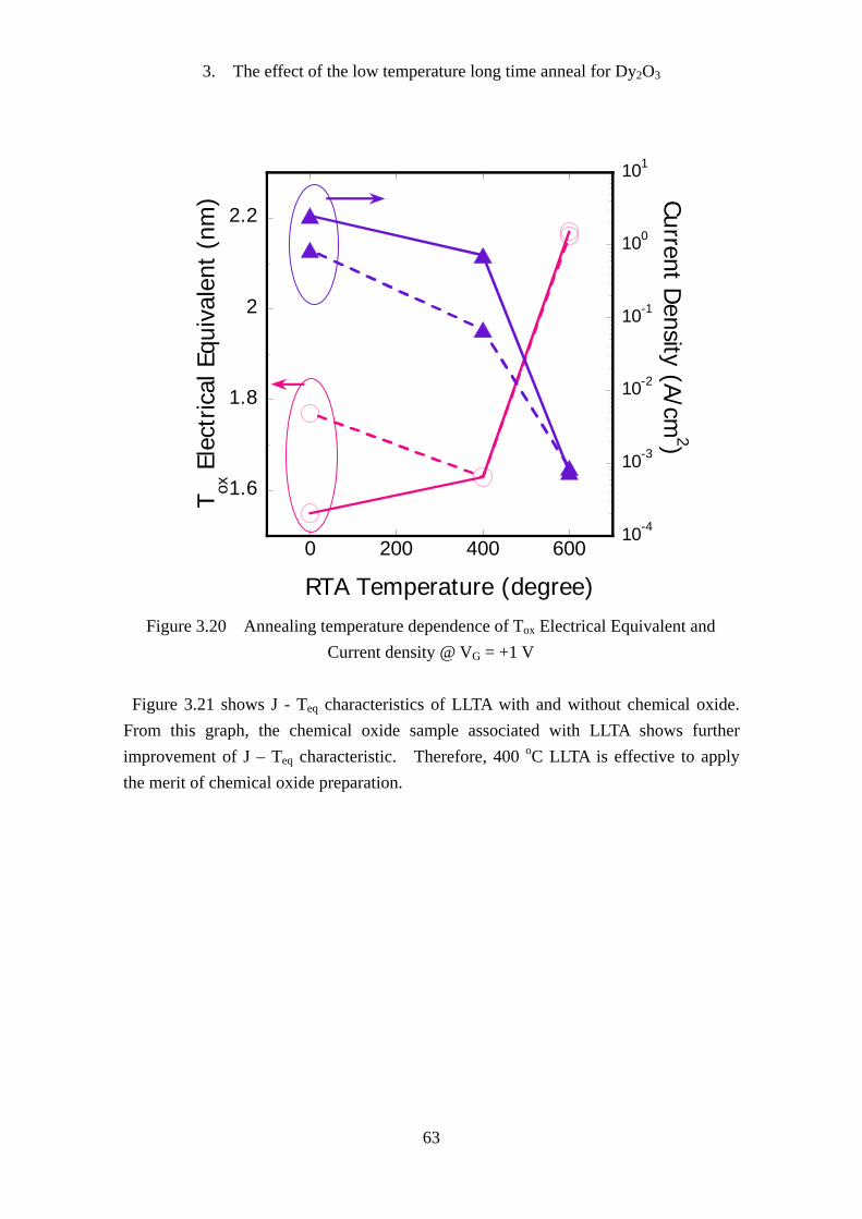
Figure 3.21 shows J - Teq characteristics of LLTA with and without chemical oxide.
From this graph, the chemical oxide sample associated with LLTA shows further improvement of J – Teq characteristic. Therefore, 400 oC LLTA is effective to apply the merit of chemical oxide preparation.

3. The effect of the low temperature long time anneal for Dy2O3
64
10-4
10-3
10-2
10-1
100
1.8 2.1
Curr
ent
Den
sity
(A/
cm2 )
Tox
Electrical Equivalent (nm)
HF last LLTA (400 oC)
With chemical oxide LLTA (400 oC)
5.5nm
5min
90min
90min
5min
600 oC 5min
600 oC 5min
Figure 3.21 J - Tox Electrical Equivalent characteristics for samples with and without
chemical oxide 3.4 Summary of this chapter As to annealing ambience, in the case of above 800 oC, N2 annealed sample shows high leakage current. AFM images suggest that surface roughness was one of the causes for the high leakage current. In regards in annealing time dependence, 400 oC 90 min annealed sample decrease the
leakage current with slight decrease of accumulation capacitance as compared with high temperature anneal. From XPS result, it was found that 600 oC 5min anneal accelerated the formation of interfacial layer as compared with LLTA with 400 oC. For the effect of the chemical oxide preparation, it was effective to reduce the leakage
current by half order of magnitude up to 400 oC RTA. However, after 600 oC RTA, the reduction was not obtained as compared with HF-last sample. So, LLTA could make good use of substrate preparation before the deposition. These results were promising, however, the accumulation capacitance was degraded
for certain after anneal even though 400 oC LLTA. It seems to be due to O2 penetration to interface between Dy2O3 and substrate.

3. The effect of the low temperature long time anneal for Dy2O3
65
Chapter 4
Fabrication and characterization of TaN
for gate electrode application If oxide films were annealed in oxygen, the interfacial layer growth could not be suppressed, over 400 oC annealing. Therefore, in order to solve this problem, the films were annealed after the gate metal deposition. In this chapter, fabrication process of TaN, thermally stable metal electrode, was researched.

3. The effect of the low temperature long time anneal for Dy2O3
66
4.1 Physical properties of TaN Tantalum nitride is a hard material, chemically inert, corrosion resistant, and has good shock- and heat-resistant properties. These properties make this material attractive for many industrial applications. In the silicon technology, TaN have been used as diffusion barriers in copper metallization against interaction between Cu and the underlying substrates, and it have been recognized as excellent barriers for the prevention of Cu-diffusion. And recently TaN is attracted as CMOS gate electrode for the next generation. As mentioned above, TaN shows good thermal stability and work function of 4.1 eV,
which is suitable for NMOS electrode. However, the work function depends on the N content and deposition method as shown in Table 4.1. Crystal systems of TaN and its lattice constant are shown in Table 4.2. TaN takes
many systems depending on N contents.
Table 4.1 Work function of reported gate metal
4.154.04.04.2Work Function(eV)
TaN (PVD) 3)Zr 1)Hf 1)TaMaterial
4.154.04.04.2Work Function(eV)
TaN (PVD) 3)Zr 1)Hf 1)TaMaterial
5.14.2~5.15.15.0Work Function(eV)
RuO2TaxRuy2)TiAlNy (y~1)TaN (CVD) 3)Material
5.14.2~5.15.15.0Work Function(eV)
RuO2TaxRuy2)TiAlNy (y~1)TaN (CVD) 3)Material
n-MOS
p-MOS
Table 4.2 Structure type of TaNx
Hexagonal
Cubic
Hexagonal
Orthorhombic
Cubic
Tetragonal
Cubic
Structure
P6/mmm
Fm3m
P63/mmc
C
Im3m
P42/mnm
Im3m
Space group
a = 0.3306α-Ta
a = 1.019, c = 0.531β-Ta
a = 0.433 TaN
a = 0.337TaN
A = 0.516, b = 0.311, c = 0.494Ta4N
a = 0.3044, c = 0.4914Ta2N
a = 0.519, c = 0.2908TaN
Lattice constants (nm)
Hexagonal
Cubic
Hexagonal
Orthorhombic
Cubic
Tetragonal
Cubic
Structure
P6/mmm
Fm3m
P63/mmc
C
Im3m
P42/mnm
Im3m
Space group
a = 0.3306α-Ta
a = 1.019, c = 0.531β-Ta
a = 0.433 TaN
a = 0.337TaN
A = 0.516, b = 0.311, c = 0.494Ta4N
a = 0.3044, c = 0.4914Ta2N
a = 0.519, c = 0.2908TaN
Lattice constants (nm)

3. The effect of the low temperature long time anneal for Dy2O3
67
Table 4.3 shows resistivity of TaNx. As increase in N content, the resistivity increases from 250 of TaN0.60 to 2700 µW-cm of TaN1.41.
Table 4.3 Resistivity of TaNx
191Ta
2700
910
330
250
Resistivity (µΩ-cm)
TaN0.60
TaN1.07
TaN1.35
TaN1.41
Ta/N ratio
191Ta
2700
910
330
250
Resistivity (µΩ-cm)
TaN0.60
TaN1.07
TaN1.35
TaN1.41
Ta/N ratio
4.2 Experimental procedure In this chapter, sputtering condition during fabrication and heat stability test were
studied. TaN was deposited on 5 nm SiO2/Si substrate by RF magnetron sputtering system. Then, samples were annealed as post metallization anneal (PMA) for ~ 800oC. These samples were characterized by 4-prove method, XRD, XPS AFM and SIMS. 4.3 Characterization 4.3.1 RF power dependence Figure 4.1 shows RF power dependence of resistivity. In the case of RF power of 70 W, the resistivity is too high (~0.1 Ωcm). As RF power increased, resistivity was improved, however. The sample, which was deposited at 180 W of RF power, exhibited resistivity of 470 µΩ-cm. It is considered that reaction energy is important to formation of TaN film by reactive sputtering.
Figure 4.2 shows XPS spectra for the samples of w/o PMA with RF power as a parameter. This result indicates that reduction of resistivity was not due to the N2 contents because all the spectra show almost same peak intensity ratio of N 1s and Ta 4p. Figure 4.3 shows XRD patterns for the samples of different RF power, 100 W, 180 W.
As compared with 100 W, the increase of peak intensity was obtained. This fact indicates the crystallization was accelerated by higher RF power. So, it seems that the

3. The effect of the low temperature long time anneal for Dy2O3
68
reduction of resistivity is due to the crystallization from this result.
102
103
104
105
60 80 100 120 140 160 180
R
esis
tivity
RF Power (W)
(µΩ
-cm
)
Deposition temperature: R.T.Ar/N 2 ratio: 8/1
Pressure during deposition: 0.6 Pa
w/o PMA
Figure 4.1 RF power dependence of Resistivity for the sample of w/o PMA
390395400405410415
Inte
nsity
(a.
u.)
Binding energy (eV)
Ta 4p N 1s
70 W
100 W
120 W
180 W
Ar/N2 ratio: 8/1 or 4/1
Pressure during deposition: 0.6 Pa RF power: 100 W
Figure 4.2 XPS spectra for the sample of w/o PMA with RF power as a parameter

3. The effect of the low temperature long time anneal for Dy2O3
69
30 35 40 45
Inte
nsity
(a.
u.)
2θ/θ (degree)
RF power = 180 W
RF power = 100 W
Ar/N 2 ratio: 8/1
Pressure during deposition: 0.6 Pa Deposition @ R.T.
f.c.c.-TaN (111) (002)
Figure 4.3 XRD patterns for the samples of different RF power
4.3.2 N2 ratio dependence In order to vary the N content, TaN was deposited at several Ar/N2 ratios of sputtering ambience. RF power dependence of resistivity with Ar/N2 ratio as a parameter was shown in Figures 4.4. As increase in N2 ratio, resistivity was increased about a quarter order of magnitude in the case of 100 W. From SIMS result, N content of sample for Ar/N2 = 4/1 increased by 20 % as
compared with 8/1 sample. The increase of resistivity was due to the increase of N content in TaN film. XRD patterns for the samples of different Ar/N2 ratio during sputtering were shown in
Figure 4.5. In the case of Ar/N2 = 4/1, the peak intensity of (100) grew as compared with 8/1 sample. From this result, it was found that the crystallization was accelerated at the ambience of Ar/N2 = 4/1.

3. The effect of the low temperature long time anneal for Dy2O3
70
102
103
104
105
106
107
60 70 80 90 100 110 120 130
R
esis
tivity
RF Power (W)
(µΩ
-cm
)
Deposition temperature: R.T.Ar/N 2 ratio: 8/1
Pressure during deposition: 0.6 Pa RF power: 100 W
Ar/N2=4/1
Ar/N2=8/1
Figure 4.4 RF power dependence of Resistivity for the sample of w/o PMA with N2 ratio as a parameter
30 35 40 45
Inte
nsity
(a.
u.)
2θ/θ (degree)
Ar/N2 = 8/1
Ar/N2 = 4/1
Pressure during deposition: 0.6 Pa RF power: 100 W Deposition @ R.T.
f.c.c.-TaN (111) (002)
Figure 4.5 XRD patterns for the samples of different Ar/N2 ratio during sputtering

3. The effect of the low temperature long time anneal for Dy2O3
71
4.3.3 Deposition temperature dependence In order to deposit film with crystallization, deposition temperature dependence was researched. A crystal film is thought to show lower resistivity as compared to amorphous. Therefore, TaN depositions were carried out at R.T., 200oC and 400oC.
Figure 4.6 shows deposition temperature dependence of resistivity of w/o PMA sample. As increase in deposition temperature, resistivity was increased for all the case. XRD (Figure 4.7) result indicates no difference between RT deposition and 400oC deposition as to crystallization. So, the increase of deposition temperature is not so dominant to the crystallization in this case. To make matters worse, the resistivity of 400oC deposition sample exhibited the increase as compared with R.T. deposited sample for each RF Power. Deposition temperature dependence of background pressure was also shown in Figure 4.6. From this result, the pressure did not vary up to 200oC, however, swelled about a order of magnitude at 400oC. Therefore, the increase of resistivity at 400oC was caused in the degradation of background pressure.
102
103
104
105
106
107
10-5
10-4
10-3
0 200 400
Background pressure (Pa)
Ar/N 2 ratio: 8/1
Pressure during deposition: 0.6 Pa RF power: 100 W or 70W
R
esis
tivity
(µΩ
-cm
)
Temperature during deposition (oC)
70 W
100 W
Figure 4.6 Deposition temperature dependence for the samples of w/o PMA with RF power as a parameter

3. The effect of the low temperature long time anneal for Dy2O3
72
20 25 30 35 40 45 50
Inte
nsity
(a.u
.)
f.c.c.-TaN (111)
2θ/θ (degree)
Ar/N2 ratio: 8/1Pressure during deposition: 0.6 Pa RF power: 100 W
400 oC
200 oC
RT
Figure 4.7 XRD patterns for the samples of deposited at R.T., deposited at 250oC
4.3.4 Thermal stability of TaN Figures 4.8 and 4.9 show PMA temperature dependence of resistivity with RF power and Ar/N2 ratio as parameters. After 800oC PMA, resistivity was degraded for all the samples. Figure 4.10 shows XPS spectra for the sample of before and after PMA. Spectrum of
800oC PMA gave no N 1s peak. So it is supposed to reaction with oxygen or H2O, which remains in PMA ambient. Figure 4.11 shows XRD patterns, before and after PMA. The crystallization of TaN –
Cubic was confirmed for the sample after 800oC PMA. However, (111) peak shift was observed. This fact indicates that the interplanar space was changed after PMA because of loss of N content.

3. The effect of the low temperature long time anneal for Dy2O3
73
103
104
105
0 200 400 600 800
R
esis
tivity
PMA Temperature (oC)
(µΩ
-cm
)
120W100W
180W
Deposition temperature: R.T.Ar/N 2 ratio: 8/1
Pressure during deposition: 0.6 Pa
Figure 4.8 PMA temperature dependence of Resistivity with RF power as a parameter
103
104
105
0 200 400 600 800
R
esis
tivity
PMA Temperature (oC)
(µΩ
-cm
)
Ar/N2=4/1
Ar/N2=8/1
Deposition temperature: R.T.Ar/N 2 ratio: 8/1
Pressure during deposition: 0.6 Pa RF power: 100 W
Figure 4.9 PMA temperature dependence of Resistivity with N2 ratio as a parameter

3. The effect of the low temperature long time anneal for Dy2O3
74
390395400405410415
Inte
nsity
(a.
u.)
Binding energy (eV)
Deposition Temperature: R.T.Ar/N 2 ratio: 8/1
Pressure during deposition: 0.6 Pa RF power: 100 W
Ta 4p N 1s
w/o PMA
After N2 800 o PMA
Figure 4.10 XPS spectra for the samples before and after PMA
30 35 40 45
Inte
nsity
(a.
u.)
2θ/θ (degree)
w/o PMA
after N2 800 oC PMA
Ar/N 2 ratio: 8/1
Pressure during deposition: 0.6 Pa RF power: 100 W Deposiiton @ R.T.
(002)f.c.c.-TaN (111)
Figure 4.11 XRD patterns for the samples before and after PMA

3. The effect of the low temperature long time anneal for Dy2O3
75
4.4 Summary of this chapter The fundamental properties of TaN film were examined. In this chapter, thermal budget test was mainly examined. As to RF power during the sputtering, it was necessary to deposit the film at high
sputtering power in order to reduce the resistivity. And it was confirmed that crystallization depended on RF power during the deposition from XRD patterns. The improvement of resistivity is due to the crystallization. For N2 ratio dependence during sputtering, the sample deposited at higher N2 ratio
shows higher N content. And the crystallization was accelerated in the case of Ar/N2 = 4/1. With deposition temperature dependence, acceleration of crystallization did not depend
on the substrate temperature (~ 400oC) in this experiment. To make matters worse, resistivity was degraded in the case of 400 oC deposition. It seems to be due to the degradation of background pressure before the deposition. And these deposited films were examined into thermal stability. The resistivity was increased over 600oC for each condition. One of the reasons
seems to be due to residual oxygen in PMA ambience, which reacted with metal during annealing.

3. The effect of the low temperature long time anneal for Dy2O3
76
Chapter 5
The effect of post metallization anneal
with a structure of TaN/Dy2O3/Si(100) If Dy2O3 film was annealed over 400 oC in O2 ambience, Tox Electrical Equivalent increased as compared with as-deposited film, as discussed in chapter 3. In this chapter, in order to solve this problem, the effect of annealing after the metal deposition was evaluated.

3. The effect of the low temperature long time anneal for Dy2O3
77
5.1 Fabrication procedure Fabrication procedure of MIS capacitor is shown in Figure. 2.1. Dy2O3 films were
deposited by electron beam evaporation in ultra high vacuum (UHV) chamber at room temperature or 250oC on n-type Si(100) substrates treated by diluted HF. Some of the samples were chemically oxidized by H2O2 dip to form 0.5 nm SiOx layer. The deposition rate of the film was about 0.7nm/min. Some of the deposited samples were then annealed at 600oC for 5 min in O2 ambient. TaN electrode was deposited on the top of the oxide. The TaN sputtering condition is shown in table 1, which was on the basis of results in chapter 4. And then, PMA (Post Metallization Anneal) was carried out at 400oC or 600oC. For gate patterning, photolithography was introduced. Metal etching condition is shown in Table 5.2. And then, Al back electrode was deposited on backside of n-Si (100) substrate.
Dy2O3 Deposition (Tsub=R.T. or 250oC)
Substrate cleaning (SPM & HF dip)
RTA
Al deposition TaN deposition
PMA
Al Back Electrode deposition
Chemical Oxide preparation(H2O2 30min)
Figure 5.1 Experimental procedure
Table 5.1 TaN sputtering condition
0.6 PaPressure during sputtering
3.8/0.48 sccmAr/N2 ratio
120 WRF power
R.T.Substrate temperature
~ 2.0 x 10⁻⁵ PaBack ground pressure
0.6 PaPressure during sputtering
3.8/0.48 sccmAr/N2 ratio
120 WRF power
R.T.Substrate temperature
~ 2.0 x 10⁻⁵ PaBack ground pressure

3. The effect of the low temperature long time anneal for Dy2O3
78
Table 5.2 Metal etching conditions (Al and TaN)
Etching ConditionMetal
RIE:1. Pressure during etching: 0.03 Torr2. RF power: 50W3. Ar/CF4 ratio: 50/50sccm4. etching time: 1 min 30sec x 7 times for 100 nm thick
TaN
Wet etching:Immerse in H3PO4 (55 o) with rate of 200 nm/30 sec
Al
Etching ConditionMetal
RIE:1. Pressure during etching: 0.03 Torr2. RF power: 50W3. Ar/CF4 ratio: 50/50sccm4. etching time: 1 min 30sec x 7 times for 100 nm thick
TaN
Wet etching:Immerse in H3PO4 (55 o) with rate of 200 nm/30 sec
Al
Figure 5.2 TaN electrode patterned by photolithography 5.2 Investigation on post metallization anneal Figure 5.3 shows C-V characteristics for TaN/Dy2O3/n-Si(100) structures. Dy2O3 film was deposited at RT. Samples, which were not annealed before metal deposition (as-depo/N2 400oC PMA),
showed higher accumulation capacitance. And hysteresis was improved by PMA, especially after 600oC PMA. On the other hand, for the sample annealed in O2 at 600oC before TaN deposition exhibited severe decrease of accumulation capacitance. Figure 5.4 shows the leakage current result for the same samples shown in Figure 5.3.
Samples of only PMA showed high leakage current of 2× 101 A/cm2 even though after the 400oC PMA, while RTA 600oC/PMA 400 oC sample exhibited low leakage current of 2× 10⁻⁶ A/cm2 @ VG = +1V. From these C-V and J-V, the formation of interfacial layer could be suppressed with
improvement of hysteresis by annealing with metal electrode cover. By this method, oxygen penetration to the interface was almost suppressed.

3. The effect of the low temperature long time anneal for Dy2O3
79
0
1
2
3
4
-1 -0.5 0 0.5 1
Capa
cita
nce
(µF/
cm2 )
Voltage (V)
as-depo/N2 400oC PMA
O2 600 oC/N
2 400oC
TaN/Dy2O
3/n-Si(100)
Figure 5.3 C-V characteristics for TaN/Dy2O3/n-Si(100)
10-10
10-8
10-6
10-4
10-2
100
102
0 0.2 0.4 0.6 0.8 1
Curr
ent
Den
sity
(A/
cm2 )
Voltage (V)
TaN/Dy2O
3/n-Si(100)
400oC 5min PMA
600oC 5min/400 oC PMA
Figure 5.4 J-V characteristics for TaN/Dy2O3/n-Si(100)

3. The effect of the low temperature long time anneal for Dy2O3
80
Additionally, LLTA was also carried out as PMA. Metal deposited samples were annealed at 400oC 5min, 400oC 90min and 600oC as PMA, shown in Figures 5.5 and 5.6. In the case of direct annealing for oxide films, LLTA was effective for the reduction of leakage current, maintaining Teq with slight increase. However, LLTA did not give the effect as PMA. Oxygen activation occurred not only
at the interfacial layer but also in the Dy2O3 film. Therefore, the effect of LLTA is dependent of the oxygen pressure
0
1
2
3
4
-1 -0.5 0 0.5 1
Cap
acita
nce
(µF/
cm2 )
Voltage (V)
400oC 5min PMA
TaN/Dy2O
3/n-Si(100)
400oC 90min PMA
Figure 5.5 C-V characteristics for LLTA sample as PMA
10-5
10-4
10-3
10-2
10-1
100
101
102
0 0.2 0.4 0.6 0.8 1
Curr
ent
Den
sity
(A/
cm2 )
Voltage (V)
TaN/Dy2O
3/n-Si(100)
400oC 5min PMA
400oC 90min PMA
Figure 5.6 C-V characteristics for LLTA sample as PMA

3. The effect of the low temperature long time anneal for Dy2O3
81
Figure 5.7 shows C-V characteristics with PMA temperature as a parameter. From this result, for the sample of 600oC PMA, a shoulder in depletion region was indicated due to interface state. These results suggest the oxygen defect was not improved by PMA because of the no
supply of oxygen from outside. And after 600oC PMA, oxygen in Dy2O3 was taken into formation of interfacial layer. Therefore, influence of oxygen defect at interface became very much.
0
1
2
3
4
-1 -0.5 0 0.5 1
Capa
cita
nce
(µF/
cm2 )
Voltage (V)
as-depo/N2 400oC PMA
as-depo./N2 600oC
TaN/Dy2O
3/n-Si(100)
Figure 5.7 C-V characteristics with vertical axis as C/Cmax In order to improve the film with low defect, the effects of high temperature deposition
of Dy2O3 and Si surface treatment by H2O2 were investigated. Figure 5.8 shows C-V characteristics for samples with and without chemical oxide
preparation. The Dy2O3 thin film was deposited at 250oC. The accumulation capacitance of 400 oC PMA sample without directly annealing for oxide in O2 ambient (as-depo/N2 400oC) exhibited excellent Tox Electrical Equivalent of 1.03 nm for sample of HF-last and 1.01 nm for sample with chemical oxide, respectively. However, the huge interface state was also indicated for the 600oC PMA case. Figure 5.9 shows J-V characteristics for the same samples shown in Figure 5.8. From
this result, the effect of the chemical oxide showed the leakage current reduction of a

3. The effect of the low temperature long time anneal for Dy2O3
82
half order of magnitude. And similar to the case of RT deposition, the samples were divided into 2 groups, whether Dy2O3 films were before the metal deposition. Figure 5.10 shows Tox Electrical Equivalent dependence of current density. From this
result, it was confirmed that 250oC deposited sample exhibited better characteristics than RT deposited sample, and the sample with chemical oxide at the interface showed further improvement.
0
1
2
3
4
5
-1 -0.5 0 0.5 1
Cap
acita
nce
(µF/
cm2 )
Voltage (V)
TaN/Dy2O
3/n-Si(100)
as-depo./N2400 oC PMA
as-depo./N2600 oC PMA
O2600 oC RTA/N
2400 oC PMA
Solid: HF-lastDotted: with Chemical Oxide
Figure 5.8 C-V characteristics for samples with and without chemical oxide preparation

3. The effect of the low temperature long time anneal for Dy2O3
83
10-10
10-8
10-6
10-4
10-2
100
102
0 0.2 0.4 0.6 0.8 1
Curr
ent
Den
sity
(A/
cm2 )
Voltage (V)
TaN/Dy2O
3/n-Si(100)
Solid: HF lastDotted: with Chemical Oxide
as-depo./N2 400oC PMA
as-depo./N2 600oC PMA
O2 600o RTA/N
2 400oC PMA
Figure 5.9 J-V characteristics for samples with and without chemical oxide
preparation
10-1
100
101
0.9 1 1.1 1.2 1.3 1.4
Curr
ent
dens
ity (
A/cm
2 )
Tox
Electrical Equivalent (nm)
RT depo. HF-last
250 oC depo. HF-last
250 oC depo.with Chemical Oxide
TaN/Dy2O
3/n-Si(100)
Figure 5.7 Tox Electrical Equivalent dependence of current density
3. The effect of the low temperature long time anneal for Dy2O3
84
5.3 Summary of this chapter In this chapter, the effect of annealing after metal deposition for slight growth of interfacial layer was confirmed. However, the oxygen defect was indicated from their negative shift and interface state after the PMA. And films deposited at 250oC exhibited the improvement as compared with R.T.
deposited films in the characteristic of J-Teq, and further improvement was obtained for chemical oxide prepared sample.

3. The effect of the low temperature long time anneal for Dy2O3
85
Chapter 6
Conclusions

3. The effect of the low temperature long time anneal for Dy2O3
86
6.1 Main results obtained from this study In the case of annealing in oxygen without electrode, 400 oC/90 min anneal decreased the leakage current with slight decrease of accumulation capacitance as compared with 600oC/5min anneal. It seems to be due to effective activation of Dy2O3. However, even the LLTA, the accumulation capacitance decreased as compared with as-depo. sample as shown in Figure 6.1. This interfacial layer shows lower dielectric constant as compared with Dy2O3 (εDy2O3
> εil > εSiO2), therefore it influences Teq strongly, as following equation (e.q. 6.1). So, Teq and leakage current should be controlled by Dy2O3 thickness itself.
22
32
32SiO
il
ilSiO
ODy
ODyeq
TTT ε
εε
ε+= (6.1)
In the case of annealing after the metal deposition, oxygen penetration to the interface was suppressed and the accumulation capacitance did not decrease i.e. the formation of interfacial layer could be suppressed by the cover of metal electrode (see Figure 6.2). This annealing method suppressed the interfacial layer thickness (Til<<TDy2O3),
therefore, Teq and leakage current could be controlled by Dy2O3 thickness. However, negative shift and interfacial state due to the defect of oxygen were indicated
for PMA only samples. These results suggest the necessity of the sufficient oxygen in Dy2O3 film of as-deposited. Finally, LLTA as PMA was not exhibited the effect of reduction of leakage current
such as annealed in O2 because sufficient activation was not given in the condition of no supply of oxygen from outside.
Si
•Providing oxygen during anneal •Growth of interfacial layer
RTA
Dy2O3 interfacial layerO2
Figure 6.1 Interfacial layer growth due to annealing in oxygen

3. The effect of the low temperature long time anneal for Dy2O3
87
Si
Dy2O3
PMA
Suppression of interfacial layer formation
TaN
Figure 6.2 Suppression of oxygen penetration by TaN metal cover
10-10
10-6
10-2
102
0.5 1.0 1.5
HfO2NH3+HfO2HfSiONZrO2Zr-SilicateAl2O3NH3+ZrO2Zr-Al-Si-OPr2O3Nd2O3Sm2O3Gd2O3Lu2O3Dy2O3La2O3SiO2Nitrided SiO2
EOT (nm)
Curr
ent
Den
sity
(A/
cm2 )
Annealingafter TaN deposition
250 oC depo with C.O.
LLTA with C.O.
10-10
10-6
10-2
102
0.5 1.0 1.5EOT (nm)
Curr
ent
Den
sity
(A/
cm2 )
Figure 6.3 J-EOT characteristics with reported data Figure 6.3 shows J-EOT characteristics with reported data. EOT of 0.65 nm with
leakage current of 1.64 A/cm2 was obtained for the film deposited at 250 oC, annealed at 400 oC after metal deposition. And for the sample of LLTA, 1.76× 10⁻⁴ A/cm2 was obtained with EOT of 1.49 nm.

3. The effect of the low temperature long time anneal for Dy2O3
88
6.2 Future study To make the film with sufficient oxygen content, the effect of radical oxidation should be investigate. And it is reported that the interfacial layer affects to carrier mobility, i.e. carrier
mobility was improved by interfacial layer. Therefore, electron mobility for with or without interfacial layer samples should be characterized by evaluating MOSFET.

3. The effect of the low temperature long time anneal for Dy2O3
89
Acknowledgements The author would like to give the greatest thanks to Professor Hiroshi Iwai for his
excellent guidance, timely inspiration, and continuous encouragement. The author would like to thank Associate Professor Shun-ichiro Ohmi very much for
the very useful discussions and advice for whole researches. The author would like to give sincere gratitude to Professor Hiroshi Ishiwara very
much for supporting author’s research. The author would like to thank Associate Professor Kazuo Tsutsui very much, who
gave the author very useful advice. The author would also thank Dr. K. Aizawa, Mr. T. Kurita and Mr. D. Shouji very
much for supporting the author’s researches. The author would specially thank Mr. N. Sugita and all the members of Associate
Professor Tokumitsu Laboratory and Professor Professor Ishiwara Laboratory for their kind cooperation and encouragement.
The author would like to express sincere gratitude to Mr. A. Genseki, Mr. K. Yoshida, Mr. S. Inumiya and Dr. T. Yano for their kind cooperation of the author’s research.
The author would like to thank research colleagues of Professors Iwai's Laboratories, Mr. J. Tonotani, Mr. K. Ohshima, Mr. Y. S. Kim, Mr. M. Takeda, Mr. S. Sato, Mr. S. Akama, Ms. I. Kashiwagi, Mr. A. Kikuchi, Ms. C. Ohsima, Mr. H. Yamamoto, Mr. I. Ueda, Mr. A. Kuriyama, Mr. Y. Yoshiaki, Mr. Hendriansyah Sauddin and Mr. J. A. NG for the useful discussions and encouragement.
The author would appreciate the official help of laboratory secretaries, Ms. K Takahashi, Ms. N. Sato, Ms. Y. Mihara, Ms. E. Furuya, Ms. K. Matsuno, Ms. K. Kubo, Ms. N. Hayashi, K. Matsuno and Ms. N. Ihzuka.
This work was partially supported by STARC (Semiconductor Research Academic Center. The author would like give thanks to Drs. N. Nakayama, T. Nishikawa, J. Yugami, T. Kitano, K. Fujita, K. Tsunashima and T. Kato for useful discussions and technical advices.
This study was partially supported by Grant-in-Aid for Scientific Research Priority Areas (A): Highly Functionalized Global Interface Integration
Finally, the author would like to give thanks to his family for their warm supports.
Junichi TAGUCHI Yokohama, JAPAN
February 2003

3. The effect of the low temperature long time anneal for Dy2O3
90
REFERENCE [1] Y. H. Kim et al., “High quality CVD TaN gate electrode for sub-100 nm MOS devices”, IEDM Tech Dig., 2001 [2] B. H. Lee et al., “Characteristics of TaN gate MOSFET with ultrathin hafnium oxide (8A-12A)”, IEDM Tech. Dig., 2000 pp. 39-42. [3] J. C. Chuang et al., “Properties of thin Ta-N films reactively sputtered on Cu/SiO2/Si substrate” Thin Solid Films 322, 1998 pp. 213-217. [4] M. Stavrev et al., “Sputtering of tantalum-based diffusion barriers in Si/Cu metallization: effect of gas pressure and composition” Applied Surface Science 91, 1995 pp. 257-262. [5] Ranjana Saha et al., “Effect of structure on the mechanical properties of Ta and Ta(N) thin films prepared by reactive DC magnetron sputtering” Journal of Crystal Growth 174 (1997) pp. 495-500. [6] H. Zhong et al., “Properties of Ru-Ta Alloys as Gate Electrodes For NMOS and PMOS Silicon Devices” IEDM Tech Dig., 2000. [7] D. G. Park et al., “Robust Ternary Metal Gate Electrodes for Dual Gate CMOS Devices” IEDM Tech Dig., 2000. [8] C. H. Lee et al., “MOS Device with High Quality Ultra Thin CVD ZrO2 Gate Dielectrics and Self-Aligned TaN and TaN/Poly-Si Gate Electrodes” Symp. on VLSI Tech., 2001 pp. 137-138. [9] C. H. Lee et al., “Self-Aligned Ultra Thin HfO2 CMOS Transistors with High Quality CVD TaN Gate electrode” Symp. on VLSI Tech., 2002 [10] S. B. Samavedam et al., “Metal Gate MOSFETs with HfO2 Gate Dielectric” Symp. on VLSI Tech., 2002 [11] JCPDS Card [12] K. Radhakrishnan et al., “Reactive sputter deposition and characterization of tantalum nitride thin films” Materials Science and Engineering B57 (1999) pp. 224-227. [13] S. Jeon et al., “Excellent Electrical Characteristics of Lanthanide (Pr, Nd, Sm, Gd, and Dy) Oxide and Lanthanide-doped Oxide for MOS Gate Dielectric Applications” IEDM Tech Dig., 2001 pp. 471-474 [14] U. Neuwald et al., “Chemical oxidation of hydrogen passivated Si(111) surfaces in H2O2” J. Appl. Phys. 78 1995 pp.4131-4136 [15] International Technology Roadmap for Semiconductors 2001 edition