jetting fluids in a wide variety of new electronics and
TRANSCRIPT

JETTING FLUIDS IN A WIDE VARIETY OF NEW ELECTRONICS AND SEMICONDUCTOR NON TRADITIONAL PACKAGING AND ASSEMBLY
APPLICATIONS
Alec J. Babiarz, Asymtek,
Carlsbad, CA, USA ababiarz @ Asymtek.com
ABASTRACT The expansion of business into alternative energy, green components, and energy efficient components is having a significant impact on the electronics and semiconductor industry. In solar cell production using wafers or printed electronics, the application of fluids to the end product is part of the function of the product rather than just a packaging process. Energy efficient lighting using LEDs depends upon the function and proper deposition of phosphor filled silicones. Fuel cell proton exchange membrane manufacturing depends upon fine and uniform film builds of carbon platinum dispersions and nafion using jet spraying technologies. Some new fuel cell technologies are being developed directly on silicon wafers for mobile power applications. As the industry continues to move to more green focused manufacturing, new materials and processes are being introduced to mitigate the high price of gold wire bonding. New energy efficient display technologies like OLEDs and the application of special films to traditional liquid crystal displays require fluids a part of the device’s function. Jetting of a wide range of materials has enabled the advancement of these new products. This paper covers a variety of new jet deposition methods of fluids used in high brightness LED manufacturing, fuel cell membrane manufacturing, photovoltaic solar cell manufacturing, OLED manufacturing, reflective film lamination for flat panel display assembly and new stacked die assembly processes. Keywords: Jet, Underfill, Fuel Cells, Stacked Die, ODF, FPD INTRODUCTION The electronics packaging and assembly industry is being affected in a positive manner as more business develops from green initiatives, alternative energy, higher energy efficiency requirements and the emergence of life science applications. There are challenges in developing alternate energy sources, higher power density, small size, low cost and the durability & reliability required by life science applications. Non contact jetting, spraying, and film coating processes are utilized to enable the function of semiconductor devices by being part of the end product’s structure or operation rather than just a package. RECENT APPLICATIONS Photovoltaic (PV) solar cells utilize several dispensing processes from the initial production stages to the final
assembly of complete panels. Beginning in the first stages, the PV wafers are uniformly sprayed with a phosphor doping material prior to entering the doping furnace. Later in the line the PV wafers must have conductive collector lines applied across the cell which are bussed together on each cell and then stitched between cells to form a panel. See Figure 1. The conductive collector lines are applied by stencil printing, electroplating from seed lines, or dispensing.
Over the last several years underfilled flip chip dies and packages have been used in life science applications such as pace makers and hearing aids to reduce size and power while increasing capability and reliability. Jetting the underfill allowed smaller keep out zones around the dies enabling tighter packaging. Currently, the emerging life science applications are in blood analysis. In these applications the semiconductor wafers have specialty die that are fluid analysis circuits that need to have chemicals jetted into wells as part of the circuits’ future function in the end device. See Figure 2.
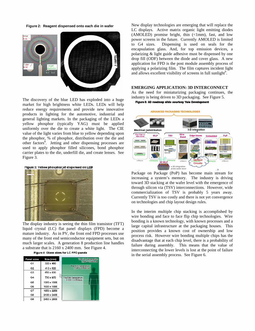
Figure 2: Reagent dispensed onto each die in wafer
The discovery of the blue LED has exploded into a huge market for high brightness white LEDs. LEDs will help reduce energy requirements and provide new innovative products in lighting for the automotive, industrial and general lighting markets. In the packaging of the LEDs a yellow phosphor (typically YAG) must be applied uniformly over the die to create a white light. The CIE value of the light varies from blue to yellow depending upon the phosphor, % of phosphor, distribution over the die and other factors8. Jetting and other dispensing processes are used to apply phosphor filled silicones, bond phosphor carrier plates to the die, underfill die, and create lenses. See Figure 3.
The display industry is seeing the thin film transistor (TFT) liquid crystal (LC) flat panel displays (FPD) become a mature industry. As in PV, the front end FPD processes use many of the front end semiconductor equipment sets, but on much larger scales. A generation 8 production line handles a substrate that is 2160 x 2400 mm. See Figure 4.
New display technologies are emerging that will replace the LC displays. Active matrix organic light emitting diodes (AMOLED) promise bright, thin (<1mm), fast, and low power screens in the future. Currently AMOLED is limited to G4 sizes. Dispensing is used on seals for the encapsulation glass. And, for top emission devices, a polarizing & light guide adhesive must be dispensed by one drop fill (ODF) between the diode and cover glass. A new application for FPD is the post module assembly process of applying a polarizing film. The film captures incident light and allows excellent visibility of screens in full sunlight9. EMERGING APPLICATION: 3D INTERCONNECT As the need for miniaturizing packaging continues, the industry is being driven to 3D packaging. See Figure 5.
Package on Package (PoP) has become main stream for increasing a system’s memory. The industry is driving toward 3D stacking at the wafer level with the emergence of through silicon via (TSV) interconnections. However, wide commercialization of TSV is probably 5 years away. Currently TSV is too costly and there is not yet convergence on technologies and chip layout design rules. In the interim multiple chip stacking is accomplished by wire bonding and face to face flip chip technologies. Wire bonding is a known technology, with known processes and a large capital infrastructure at the packaging houses. This position provides a known cost of ownership and low process risk. However wire bonding multiple chips has the disadvantage that at each chip level, there is a probability of failure during assembly. This means that the value of interconnecting the lower levels is lost at the point of failure in the serial assembly process. See Figure 6.

A new jetting technology provides an interconnection process that is more reliable and cost effective. By jetting silver epoxy along the edge of the stacked die, interconnection is made between all die in the stack. See Figure 7.
One example of this process is provided by Vertical Circuits Inc. (VCI). On a memory package that required 8 stacked die, the wire bond process employed 22 process steps versus 8 for the vertical interconnect. See Table 1 and Table 2.
Operation i/b Step Sq.Ft Man UPH #Mch Str.CT
Die Attach 1 (Mother + 25um DAF) i DA1 32 0.5 420 2 789
Die Attach 2 (Daughter + 10um DAF) i DA2 32 0.5 460 2 720
Plasma 1 (Pre WB) b PL1 18 0.25 1 600
Wire-Bond 1,2 (Std. + RBSoB) i WB1 20 0.25 140 4 2366
Plasma 2 (Pre FOW) b PL2 18 0.25 1 600
Die Attach 3 (Daughter + FOW) i DA3 32 0.5 460 2 720
Die Attach 4 (Daughter + 10um DAF) i DA4 32 0.5 420 2 789
Cure FOW b CR1 18 0.25 1 24600
Plasma 3 (Pre WB) b PL3 18 0.25 1 600
Wire-Bond 3,4 (Std. + RBSoB) i WB3 20 0.25 100 5 3312
Plasma 4 (Pre FOW) b PL4 18 0.25 1 600
Die Attach 5 (Daughter + FOW) i DA5 30 0.5 460 2 720
Die Attach 6 (Daughter + 10um DAF) i DA6 30 0.5 420 2 789
Cure FOW b CR2 18 0.25 1 24600
Plasma 5 (Pre WB) b PL5 18 0.25 1 600
Wire-Bond 5,6 (Std. + RBSoB) i WB5 20 0.25 100 5 3312
Plasma 6 (Pre FOW) b PL6 18 0.25 1 600
Die Attach 7 (Daughter + FOW) i DA7 32 0.5 460 2 720
Die Attach 8 (Daughter + 10um DAF) i DA8 32 0.5 420 2 789
Cure FOW b CR3 18 0.25 1 24600
Plasma 7 (Pre WB) b PL7 18 0.25 1 600
Wire-Bond 7,8 (Std. + RBSoB) i WB5 20 0.25 85 6 3896
22 1084 16 46 39Steps Sq.Ft Men Mach. Hours
TOTAL (FOW)
8-Die 1mm FOW NANDTable 1: Stacked Wire Bonding Process
Operation i/b Step Sq.Ft Man UPH #Mch Str.CT
Die Attach 1 (Mother + 25um DAF) i DA1 32 0.5 590 1 561
Die Attach 2-8 (Daughter + 10um DAF) i DA2 32 0.5 115 5 2880
Plasma 1 (Pre-Coat) b PL1 18 0.25 800 1 414
Parylene Coat b CT1 60 0.5 1 7500
Laser Ablation i LS1 60 0.5 416 2 796
Plasma 2 (Post-Laser/Pre-ViP) b PL1 18 0.25 800 1 414
Vertical Interconnect Process i VI1 20 0.5 140 4 2366
Cure ViP b CR1 18 0.25 1 3600
8 258 8 16 8Steps Sq.Ft Men Mach. Hours
TOTAL (VCI)
8-Die 1mm VCI NANDTable 2: Jetted interconnect for stacked die
The wire bond process also required 101m2 of floor space with 16 operators on 46 machines resulting in 39 hours of cycle time versus 24m2 of floor space with 8 operators on 16 machines with an 8 hour cycle time for the vertical interconnect process. The interconnection uses jetting 200 micron wide lines of silver epoxy instead of using gold wire bonds. EMERGING APPLICATON: FUEL CELLS A new application for semiconductor wafer processing is the development of micro direct methanol fuel cells (μDMFC). The driving market force for DMFC is for the replacement or recharging of batteries in portable and handheld devices. The technology driving DMFC is that its volumetric energy density (800Wh/kg) is greater than Lithium batteries (200Wh/kg) and by using a readily available fuel as the electron generator; the user’s mobility is increased because a battery charging outlet is not required. The commercialization of a μDMFC is dependent upon a successful fuel cell technology implementation, and a valid commercial partnership between a semiconductor supplier, market leading handheld device supplier and a properly packaged fuel cartridge. Recently, BIC (lighters), Nokia and ST Microelectronics have begun to work toward developing and bringing the μDMFC to market sometime in 2009. A DMFC works by reducing methanol and water at the anode side of a catalyst film allowing the proton exchange to occur through a membrane in contact with the oxidation side at the cathode catalyst film. The electrons necessary for the complete reaction flow through the completed circuit like a battery. Figure 8 shows a schematic diagram of a fuel cell and the chemical reaction.

Figure 8: Chemical reactions and DMFC schematic
Semiconductor and micro electro mechanical systems (MEMS) manufacturing processes are particularly suited to making μDMFCs. Figure 9 shows a diagram of a semiconductor based fuel cell.
On the anode side, the silicon wafer is etched with holes to allow a path for water and methanol to diffuse into the catalyst layer. The semiconductor anode has conductors deposited by standard deposition techniques. In some designs the Platinum and Ruthenium (Pt and Ru) catalyst are deposited as well. But in most cases a porous catalyst layer laden with carbon particles, that have Pt and Ru attached, is deposited or placed on the anode. In some cases the layer is a separate sheet of carbon catalyst film placed in intimate contact with the anode. Figure 10 shows 9 steps to fabricate a typical semiconductor DMFC.
The proton exchange membrane (PEM) is composed of Nafion. Nafion is a DuPont product which is a perfluoro sulfonic acid polymer that has low gas permeability and high proton conductivity. The cathode side uses basically the same catalyst and gas diffusing layers. The cathode semiconductor side may have channels and or holes to allow oxygen in and water out. In a DMFC, the anode side requires water. An optimally designed device reuses the oxidation side’s water byproduct at the anode reduction side. Also, it is possible to design the device for passive flow of fuel, water and air (oxygen) so no external pumping is required. There are many papers on different configurations of μDMFC using semiconductors3,4,5,6,7. In some devices the catalyst layer is dispensed as a carbon black ink and the Nafion polymer PEM is dispensed as a fluid in solution with a solvent. It is challenging to apply these materials. The carbon particles in the ink tend to settle or conglomerate causing jet nozzle clogging issues. The solvent based Nafion flashes off quickly causing clogging issues in the jet nozzles. In addition, the Nafion contains an active sulfonic acid that reacts with most wetted dispensing parts causing poisoning, bubbles and deterioration of the dispensing system. In addition there are challenges with the fluids’ various interactions with the substrates. The carbon ink may not wet to improperly prepared surfaces and it becomes brittle as it dries. The wetting issues can be resolved with standard substrate cleaning by plasma or alcohol/acetone washes.

However, as the ink dries it becomes brittle. If the ink layers are too thick, the outer layer dries much faster than the inner layers causing cracking similar to water based conformal coatings. Ink jetting heads have been used to apply the carbon catalyst inks. Unfortunately, ink jets apply ink with very small drops (8 pico liters) which requires more time to dispense. This problem was solved by using jet valves from the underfill dispensing applications. The jet valve can apply ink in adequate thicknesses in one or two pases that do not crack but also meet the throughput needs. See Figure 11.
Also, the automated dispenser should have a mass flow calibration function to keep adequate control on the amount of ink that is applied as the catalyst density is important for good fuel cell operation. Most of the inks also contain a small amount of Nafion which requires the wetted parts of the jet valves to be passivated. Standard ink jet heads available in the market cannot be adequately passivated for long term use which is another limiting factor for standard ink jets. Nafion application has challenges in dispensing as well as the after dispensing surface interactions. Since the Nafion solution is volatile, the jet valve must be managed properly by the automated dispenser so the nozzles do not plug with cured Nafion. The jets wetted parts must be a material set that is highly compatible with sulfonic acid. Once the valve and automated dispenser are adequately configured, the deposition of the Nafion presents new issues. The typical cured PEM layer of Nafion is between 30 to 100 microns thick, depending on the fuel cell design. If the Nafion is dispensed in one film pass it may flow outside is bounds or not wet a particular area. As the nafion dries the outer edges dry first this creates a film layer that looks like a bathtub. This problem can be mitigated by using a dam and fill technique. There are a multitude of patterns that must be empirically determined as different formulations of Nafion/solvent present different drying characteristics. The automated dispenser should offer an
easy means to fill the desired shape to keep the bathtub shape to a minimum and keep the inner surface flat. By using different patterns of fill a dry film thickness of 30 microns +- 5 microns is possible. Figure 12 shows wet Nafion on carbon ink catalyst layer and Figure 13 shows a typical dry Nafion profile.
CONCLUSIONS: The ability to jet adhesives has enabled new semiconductor packaging processes. The ability to jet silver epoxy along a stepped edge provides a cost effect method to stack 8 or more die.

Semiconductor devices are moving out of the traditional market of being just an integrated circuit. In life science markets the integrated circuit of a sensor has a dispensed reagent as an active part of the circuit. Semiconductor processes are enabling new applications further outside the traditional use of wafer processing. The μDMFC could not exist without using semiconductor conductive layer deposition and etching processes. Furthermore, dispensing of liquids such as catalyst inks and Nafion PEMs enable the end device to function as a fuel cell. The part of the package that is dispensed is a functional part of the end device. The applications for jetting fluids keep increasing and enabling new products which further the expansion of semiconductors outside integrated circuits. ACKNOWLEDGEMENTS: Asymtek New Business Development Team: Don La, Dave Mejia, Brian Sawatzky, Able Gomez, Rick Horwath and Jim Klocke. Developed the jet and process technology for carbon ink and Nafion dispensing. REFERENCES:
1. Peter N. Pintauro and Ryszard Wycisk, Department of Chemical Engineering, Case Western Reserve University, “Polymeric Membranes for Fuel Cells: Overview and Future Outlook”
2. G. Q. Lu, C. Y. Wang, Penn State Univ. “Electrochemical and flow characterization of a direct methanol fuel cell”, Journal of Power Sources, 134 (2004) pp 33-40.
3. J. Santander, N. Sabate, N. Torres, J. P. Esquivel, I. Gracia, P. Ivanov, L. Fonseca & C. Cane, Centro Nacional De Microelectronica (CNM-1MB), CSIC, Bellaterra ,Spain, “Towards a Monolithic Micro Direct Methanol Fuel Cell”, IEEE Sensors 2008 Conference, 1-4244-2581, pp 37-40.
4. Agilent Technologies, Semiconductor Manufacturing Technology – Elite Development, “A Silicon-based Air-breathing Micro Direct Methanol Fuel Cell using MEMS technology. pp1-10
5. Xiaowei Liu, Chunguang Suo, Yufeng Zhang, Haifeng Shang, Weiping Chen, Xuebin Lu, “Application of MEMS Technology to Micro Direct Methanol Fuel Cell”, DTIP of MEMS and MOEMS, Stresa, Italy, 26-28 April 2006.
6. G. Q. Lu, C. Y. Wang, T. J. Yen, X. Zhang, Penn State Univ. “Development and Characterization of a Silicon-Based Micro Direct Methanol Fuel Cell”, Electrochimica Acta 49 (2004) pp821-828.
7. Didier Marsacq, “Micro-Fuel Cells”, Technical Research Division, CEA Grenoble Center.
8. Horatio Quinones, Brian Sawatzky, et al, Asymtek, “Silicone-Phosphor Encapsulation for High Power
White LEDs”, SMTA, Pan Pacific Conference, 2008
9. DuPont Displays, 10. Vertical Circuits Inc.