ipsr-i 2020 overview - amazon s3 · purple brick wall figure 4 overview of datacom drivers in...
TRANSCRIPT

An initiative of:
IPSR-I 2020 overview


3
Introduction . . . . . . . . . . . . . . . . . . . . . . . . . . . . . . . . . . . . . . . . . . . . . . . . . . . . . . . . . . . . . . . . . . . . . . . . . . . . . . . . . . . . . . . . . . . . . . . . . . . . . . . . . . . . . . 5
1 . Applications . . . . . . . . . . . . . . . . . . . . . . . . . . . . . . . . . . . . . . . . . . . . . . . . . . . . . . . . . . . . . . . . . . . . . . . . . . . . . . . . . . . . . . . . . . . . . . . . . . . . . . . . . 6
2 . Front-end technology . . . . . . . . . . . . . . . . . . . . . . . . . . . . . . . . . . . . . . . . . . . . . . . . . . . . . . . . . . . . . . . . . . . . . . . . . . . . . . . . . . . . . . . . . . . 16
3 . Back-end technology . . . . . . . . . . . . . . . . . . . . . . . . . . . . . . . . . . . . . . . . . . . . . . . . . . . . . . . . . . . . . . . . . . . . . . . . . . . . . . . . . . . . . . . . . . . . 24
4 . Product and design . . . . . . . . . . . . . . . . . . . . . . . . . . . . . . . . . . . . . . . . . . . . . . . . . . . . . . . . . . . . . . . . . . . . . . . . . . . . . . . . . . . . . . . . . . . . . . 36
Table of content

4

IPSR-I 2020 overview 5
Introduction
The objective of the IPSR-I is to establish and sustain a trust
based global network of Industrial and R&D partners, who
are working together on defi ning and creating future Photonic
Integrated Circuit (PIC) technology and systems requirements.
They jointly enable faster technology and application devel-
opments in this emerging business, guided by an up-to-date
technology and application roadmap for future developments.
This executive summary provides an overview of the most
important developments as described in the full roadmap.
The roadmap shows the functional performance requirements
of the applications (shown below in blue) and the technologies
with which these can be created (orange). The modules and
systems are the interface between the application manufac-
turers and Integrated Circuit industry; it at this interface the
functional performance parameters are converted to compo-
nent requirements and vice versa.
The IPSR-I displays the consensus of more than 250 experts from
all over the world, representing an equal mix of large multina-
tionals, small & medium enterprises, institutes and universities.
It gives an overview of the current status of technologies and
of applications in which integrated photonic components are
used. Above all it describes the trends, expectations and needs for
technology and application development in the near (0-5 years),
intermediate (5-10 years) and far (10-20 years) future.
CONTINENTOF PARTICIPANTS
PARTICIPANTS PERORGANIZATION TYPE
NorthAmerica
Europe
Asia &Oceania
Universities
Institutes
Largecompany
SME
The roadmap document is a merger between previously sepa-
rately produced roadmaps: the IPSR by AIM Photonics from the
USA and the WTMF by Photon Delta from Europe. Apart from
joining both roadmaps, it has obtained a thorough update based
on 32 workshops and countless online working group meetings.
However, the IPSR-I is a living document that is continuously
updated. The chapters need enrichment with technological and
application developments in their respective fi elds. A continuous
call is open for contributions by experts in the various techno-
logical and applicational fi elds to update the IPSR-I. The feed-
back form for submissions can be found in the Appendix.
Applications
Market Applications
FUNCTIONAL INTEGRATION MODULE INTEGRATION WAFERSCALE INTEGRATION
PI Systems PI Modules
Standard BBB’s
Sensors
PI Circuits
Tele/Datacom
Aerospace
Automotive
Biosensors & medical
(Industrial)IoT
Back-end Processing
Interconnects
Assembly
Packaging
Testing
Front-end Processing
EPDA
Platforms:
SiPh
SiN
InP
Polymers
Figure 1 Overview of roadmap structure

Hoofdstuk 1
6
Chapter 1
Applications

IPSR-I 2020 overview 7
The functional performance requirements of the PIC-users are
important factors in determining the roadmap for future devel-
opment of PIC-technology. The IPSR-I 2019 describes the main
functional performance requirements of the various applica-
tions and translates these into the technological needs and
challenges to satisfy these requirements. The IPSR-I describes
applications that will drive the development of PIC technology.
They can be divided into high and low mix applications. Both of
these types of driver applications can result in high production
volumes ; high-mix applications are typically made in many
small batches of many different products while the low-mix
applications are generated in large volumes of the same design.
The low-mix applications (datacenters, 5G and LiDAR) typically
have clear industrial roadmaps which are laid out by large
companies. Currently, the main driver for integrated photonic
devices are the datacenter transceivers in which the improve-
ment of the performance (400 Gb/s in 2021, 1 Tb/s in 2025)
is critical to the users. The low mix applications comprise
satellite communication, (medical) biosensing and mechanical
sensing. The graph above gives a rough overview of applications
based on their expected mix and volume.
For as yet, there is no consensus amongst experts on which
driver type of applications will be most dominant business
driver since the high mix – low volume applications typically
generate a high added value while the low mix – high volume
applications typically generate large revenues. But currently
datacom is the main driver for technological developments,
because the roadmap of the functional specs are clearest
defi ned. A market that is expected to be a next major driver
is the market of devices enabling the (Industrial) Internet of
Things ((I)IoT) paradigm. The market of IoT devices will com-
prise a large variety of sensors integrated with low loss wireless
connectivity solutions for operations without external power
supply. This market is typically characterized by low prices and
high volumes.
One of the main characteristics explaining the large diversity of
integrated photonic technologies is the wavelength of the light
at which applications operate best. Below you fi nd an overview
of the applications and their wavelengths.
Wave lengthUV
0 400 714 3000 50.000 200.000λ[nm]NIR IR Far IRVIS
Applicationarea Water transparancy
BIO photonics
Tele/datacom
N-ON-O
O-HO-H
C-H S=
Molecular finger printsISO 20437 definitions:UV: Ultra-VioletVIS: VisibleNIR: Near InfraredIR: Infrared
Figure 3 Wavelength of operation for applications1)
1) Partial information from: Munoz P. Photonic integration in the palm of your hand: Generic technology and multi-project wafers, technical roadblocks, challenges and evolution; Proceedings of the 2017 Optical Fiber Communications Conference and Exhibition (OFC); Los Angeles, CA, USA. 19–23 March 2017; pp. 1–3
MIX(number of designs)
VOLUMEPER DESIGN
High
High
Biosensing
Satcom
Lidar
5GDatacom
MechanicalSensingLow
Low
Figure 2 Schematic sketch of applications in the volume VS mix landscape

8
Datacenters (driving application: transceivers)
Introduction: The explosion of data generated by the growth in
social networks and digital entertainment, cloud-computing,
and IoT are the root cause of the growth of data center capacity
and the need for high bandwidth, low-latency, low power fi ber
optics based communications. This has changed the dynam-
ics of the market of communication equipment to the point
that telecommunication companies are no longer driving next
generation technology platforms and metrics, but the datacom
market (the datacenter industry (Web 2.0), fi red by social media
companies such as Google, Facebook, Microsoft, Amazon etc.).
These forces are transforming the data center architectures
towards a higher level of integration of photonics components.
Current status: Today, fi ber-optic networks are established by
a combination of long, medium and short haul optical inter-
connects that range from 3 meters to over 1000 km. PICs are
expected to take a higher share of the market, because of the
drive towards smaller photonic component solutions, lower
power consumption, higher data rates, and economics in terms
of decreasing cost per Gbps.
The datacom industry today are gearing up for 400Gbps sys-
tems using 30-40GHz photonic devices. Customers are expect-
ing data rates to continue to move quickly beyond 400 Gbps,
800 Gbps and even 1600 Gbps. Some companies even mention
the need for 3200 Gbps today. The obvious yet most diffi cult
next move is to revisit increasing the optoelectronic device
speed, and those speeds in particular that are driven not from
30-40 GHz optical bandwidth, but 80-100+ GHz (typically 40
GHz corresponds to 50 Gbps NRZ and 80 GHz corresponds to
100 Gbps NRZ). Today’s roadmaps are expressing the desire,
but at the same time doubts about getting beyond 50 GHz.
Modules/TxRxData rate density
Form factor
2019 2020 2022 2024 2026 2028
Typical linkreach Indwish
(@400Gbps)Industry plan
Typical linkreach Indwish
(@400Gbps)Industry plan
InP Monolithic
SiP& InP/SiGehybrid
Polymer Photonics
Dielectric Photonics
GaAs (VCSEL)
400Gbps 800Gbps 1600Gbps
25 Tbps/1U 100Tbps/1U 400Tbps/1U 1600Tbps/1U
3200Gbps
Q/OSFP OSFP/OBO/CP OBO/CP Co-Pkg/CoB Micro-Co-Pkg/CoB
<10km <10km <2km <2km <2km$2/Gbps $1/Gbps $0.5/Gbps <$0.2/Gbps
$0.5/Gbps $0.2/Gbps
<$0.25/Gbps <$0.05/Gbps
100GHz
<$0.25/Gbps <$0.15/Gbps
>$5/Gbps (<2km) <$2/Gbps
10-100m 5-50m 1-25m<$1/Gbps
<$1/Gbps<$0.5/Gbps
100 devices25GHz 50GHzPIC WDM Tx & Rx (30GHz)NRZ/PAM4NRZ/PAM4-83” Wafer/fab
1000 devices 1000 devices 100.000 devices
100.000 devices
100.000 devices
OEIC Intdriver/TIA 70GHz
15” Wafer/fab
10.000 devices
1000 devices 10,000 devices
1000 devices 1000 devices
8 ” Wafer/fab
OEIC Intdriver/TIA
100 devices 1000 devices70GHz (100Gbps) 70GHz (400Gbps)
VCSEL PIC 50GHzNRZ/PAM4-16
10 devices 100 devices 1000 devices
NRZ/PAM4-16
NRZ/PAM4-16
70GHz 90GHz
OEIC Intdriver/TIA (SiP/InP) 50GHz OEIC Intdriver/TIA (Sip/InP) 70GHz (serial
OEIC Int. driver/TIA 50Gbps OEIC Intdriver/TIA 100Gbps (70GHz) OEIC ASIC 50Gbps (50GHz)
Coherent client-side
Coherent client-side
(50GHz)NRZ/PAM4-16 Coherent client-side
8” Wafer/fab?
15” Wafer/fab?10,000 devices
OEIC ASIC 70GHz
8” Wafer/fab
70GHz (VCSEL-Mod)VCSEL PIC 70GHz (100Gbps)Coherent client-side
Slanted Red Font: Major industry efforts are required for commercialization= Technology cost barrier
OEIC Int. driver/TIA 50Gbps (50GHz) OEIC Intdriver/TIA 100Gbps (serial)NRZ/PAM4-16 Coherent client-side Coherent DSP-less8” Wafer/fab 8 & 12” Wafer/fab
4” Wafer/fab 4 & 6” Wafer/fab
8” Wafer/fab 8 & 12” Wafer/fab
70GHz (laser-Mod) 100GHz
70GHz 70GHz (400Gbps)
(150Gbps serial)
4” Wafer/fab 4 & 6” Wafer/fab10 devices25GHz 50GHzPIC WDM Tx & Rx (30GHz)NRZ/PAM4NRZ/PAM4-86” Wafer/fab
25GHz 50GHz (Laser-Mod)PIC WDM/MZ Mod Tx & RxNRZ/PAM4NRZ/PAM4-83-4” Wafer/fab
100 devices25GHz 50GHzPIC Tx & RxNRZ/PAM4NRZ/PAM4-86” Wafer/fab
100 devices25GHz 50GHzVCSEL PIC 25GHNRZ/PAM4NRZ/PAM4-86” Wafer/fab
Purple Brick Wall
Purple Brick Wall
Purple Brick Wall
Purple Brick Wall
Purple Brick WallPurple Brick Wall
Purple Brick Wall
Purple Brick Wall
Purple Brick WallPurple Brick Wall
Purple Brick Wall
Purple Brick Wall
Purple Brick Wall
Purple Brick WallPurple Brick Wall
Purple Brick Wall
Purple Brick WallPurple Brick Wall
Purple Brick Wall
Purple Brick Wall
Purple Brick Wall
Purple Brick WallPurple Brick Wall
Purple Brick Wall
Purple Brick Wall
Purple Brick Wall
Purple Brick Wall
Purple Brick WallPurple Brick Wall
Purple Brick Wall
Purple Brick Wall
Figure 4 Overview of datacom drivers in relationship to photonic integrated chip2)
2) Courtesey of Lightwave Logic

IPSR-I 2020 overview 9
Main challenge: The data bandwidth demand is resulting in
systems with ever higher interconnect speeds, even as processor
speed is staying constant. Data centers need to reduce their
power consumption and resulting heat generation and opera-
tion costs while also managing the total cost of ownership of
these systems while increasing reliability. Adding to this, data
centers have an increasing number of systems residing in an
environment of higher temperature and humidity which is also
subject to corrosive elements. The resulting technological chal-
lenge is that the technologies need to be able to support faster
photonic devices of 80GHz that can operate 100Gbps NRZ or
200Gbaud PAM-4.
Needs: Photonic packaging technology must improve substan-
tially to achieve the new performance requirements for exam-
ple by co-packaging and on-board optics. Data centers need
faster optical devices (such as 80GHz components), higher
integration levels, higher reliability, lower power consumption,
a higher degree of scalable economics that address $/Gbps
metrics, and smaller more miniaturized foot-print platforms.
This is enabled by a higher level of integration, e.g. by hybrid
integration of components made out of different technologies.
Needs < 5 years
• Device speed increased (bandwidths EO S21 of 80GHz in PIC platform)
• Drive voltage at 1V so that drivers can be eliminated• Telcordia qualification for modulators• Hybrid integration with InP lasers
Needs 5-10 years
• Device speed increased (bandwidths EO S21 to 120GHz+ in PIC platform (for 150Gbps NRZ data rate))
• Drive voltage less than 1V so that drivers can be eliminated (direct drive from CMOS ICs)
Needs > 10 years
• Device speed increased (bandwidths EO S21 to 150GHz+ in PIC platform (for 180Gbps NRZ data rate)
• Drive voltage less than 1V so that drivers can be eliminated (direct drive from CMOS ICs)
• Telcordia qualification for polymer modulators

10
(Industrial) Internet of Things (Driving applications: (Bio)sensing & wireless communications)
Introduction: ‘IoT’ is a system consisting of a network of
sensors, actuators and ‘smart objects’ connecting “all” things,
including every day and industrial objects in such a way as to
make them intelligent, programmable, and more capable of
interacting with humans and each other. IoT devices are being
developed for the consumer market (wearables), transport
(autonomous vehicles, logistics, smart homes, buildings and
cities, (mobile) healthcare, and the manufacturing industry.
They will revolutionize how we use the internet and drive rapid
economic growth. Smart Sensors with on-board or remote
signal processing combined with artifi cial intelligence (AI) to
trigger automated actions enable the next industrial revolution.
This revolution will lead to a paradigm shift in technology
requirements, having many devices leads to larger amounts of
decentralized data and improved quality of data security devices.
IoT products themselves will be developed from existing applica-
tions in sensing and communication.
Even though other technologies (wireless communication,
MEMs and other sensor materials) are already part of the IoT
landscape, photonic components and photonic integrated cir-
cuits have a substantial role to play in expanding the required
network capacity and in developing high-performance, minia-
turized, smart photonic sensors.
UPS, batteries,generators, fuel cells,
ambient energy harvesting, telemetry,
power stations, smart grid,
quality control
Meters, drills Supply anddemand
Recourceautomation
Publicenterprise
Equipmenttracking
Emergencyservices
Publicinfrastructure
Mining, oiland gas
Alternativeenergy
Smartenergy
Smartindustry
Smartnetworks
Defense& publicsafety
Smarthealth
Industries and sectors Application groups Devices
Smartcity
Smartfarming
Smarttransport
Smartliving
The internetof things
Smartretail
In vivo / homeresearch Traffic
control
Connectedcommunity
Cityinformation
model
Entertainment
Buildings Surveillance
Logistics Processes
Safety Stores
Assisted driving
Mobile ticketing
Transportsystems
(non-vehicularand vehicular)
Awareness
Efficiency
Care
Leisure Agriculture
Environment
Solar panels, turbinesand windmills
Digital camera’s,TVs, MP3s,
gaming consoles
Power systems,sockets, alarms
Thermostats,refrigerator, ovens,
e-readers anddesktops,
washers/dryers,lights
Wearables, wellnessmonitors, trackers
MRIs, PDAstelemedicine,
medical devices,implants,
surgical equipment,chronic diseases
RFID and NFCsupply chain
control,inventory tracking
HVAC,fire andsafety
security,acces
Securitymonitoring,purchases,production,
transportation,storage, sales
and after-sales,climate control
Pumps, valves,pipelines motors,
robotics,fabrication,assembly,packaging,
vessels, tanks
Servers andstorage,PCs andtablets,
smartphones,switches and
routersPBXs
Resourceallocation, threat
analysis, troopmonitoring,
intrusion detection
Cars, Jeeps,ambulances, tanks, fighter jets, radios,
tactical devices, storages incompatibility
detection
Homeland security,border security, fire-fighting, search and rescue, medical
crisis, disaster relief, battlefield communications,
mission critical voice,energy harvesting
Environmentalmonitoring, law enforcement
and public protection
POS terminals, cash registers, tags, vending
machines, cameras, signs, customer experience and
focused market
Robot taxi
Item location, anti-theft,NFC payment
Socialnetworking,
historicalqueries, losses
and thefts
Smart gyms,socials sports,
smart museums,enhanced
game rooms
CCTV,structural
health,noise maps,
waste management
ITS,traffic flow,congestion avoidance,
smart parking
Weather prediction,
species tracking
Soil analytics,fleet, storage (water and
fuel tanks) and waste management, livestock
monitoring, fish farming, forestry
Vehicles, lights, ships,planes, signage,
tolls, condition based maintenance,
usage based design,pre-sales analytics,
real-time routing and tracking
Figure 5 Proliferation of devices and applications in the Internet of Things (IoT)3)
3) Fraga-Lamas, Paula. (2017). Enabling Technologies and Cyber-Physical Systems for Mission-Critical Scenarios. 10.13140/RG.2.2.22769.79202.

IPSR-I 2020 overview 11
Current Status: The number of devices currently connected to
the internet per person is 4~5. Rapid growth in the consumer
market takes advantage of existing networks to connect weara-
ble devices (e.g. smart watches for health care monitoring) and
home or office wireless networks for environmental monitoring
and control, and security and access monitoring. Internet
Protocol version 6 (IPv6) together with 5G and narrower band
networks are being developed to deal with the anticipated
growth in the number of addressable IoT devices and data traf-
fic, and the required end-to-end quality of service (particularly
for mission critical applications in health care, autonomous
vehicles and security).
Sensors are already in development or marketed for integration
in consumer goods (infotainment, wearables, food and water
quality), eHealth (blood, breath and other chem-bio sensor
analysis), energy and building automation, industrial (man-
ufacturing) automation and structural monitoring, environ-
mental monitoring (oil and gas distribution, drugs, hazardous
materials and climate change). In transportation, visible and IR
imagers for highway monitoring along with LIDAR and other
sensors are already being developed for autonomous vehicles.
Main Challenges: (Network capacity and reliability) IoT is
anticipated to grow rapidly to the point where cities will have
one smart “thing” per square meter. New wireless cellular net-
works will need to deal with this device density and volume of
data generated by it. End to End Quality of Service must address
high reliability, low latency and a sufficiently high data rate to
securely handle bidirectional data for each application. Mission
critical applications require round trip data exchange of~ 1
millisecond or less. Managing minimal service interruptions for
mobile users (e.g. in automobiles and trains) is an additional
networking requirement.
(Low costs, size, Weight and Power Consumption)
The actual IoT devices contain some kind of sensor and a (5G
wireless) datacom unit. The photonic components and PICs
required for these expanded 5G networks and IoT sensors will
need to take into account demands on Cost, Size, Weight and
Power consumption.
(Data security)
Security of the data and network has been recognized as critical
for successful adoption of this technology, for example where
critical infrastructure is controlled. Blockchain and soft-cryp-
tography will secure data for the time-being, with quantum
photonics being a potential longer term solution.
Needs: If the amount of installed fiber will explode mainly to
support shorter access links within cities, the required inte-
grated photonic devices having a smaller size and lower cost will
need to be developed. Sensors which are self-powered (energy
harvesting) where appropriate will need to become cheaper,
faster and better performance to help drive demand. Sensing
functions will also need to be integrated with wireless con-
nectivity functionality and some level of signal processing so
standardized information, not raw data, is transmitted through
networks.
Sensors will need to become solid-state, miniaturized, and dras-
tically lower cost for significant consumer market penetration
and eventual full autonomy.
< 5 year Needs
• Secure data transmission protocols• Increased network capacity for IoT data• Higher wireless bandwidth, low latency• Sensors with sufficient sensitivity, accuracy and specificity
5-10 year Needs
• Localised signal processing• Low-C SWaP• Miniaturized systems (packaging)• Portability, power autonomy for mobile applications
Needs > 10 years
• Real-time data analysis and use of AI• Localised decision making

12
Automotive (Driving applications: LiDAR & wireless communications)
The opportunities for Integrated photonic modules can be
found in Advanced Driver Assistance Systems (ADAS) which
helps the driver to safely navigate their journey. Eventually
these ADAS systems might not require a driver anymore,
making the cars fully autonomous. The two main opportunities
for PICs within the ADAS systems is improving the quality of
LiDAR for an acceptable cost point, and fully integrate the car’s
systems in intra- and inter-car communication networks. There
are also opportunities for environmental sensors like air and
oil quality, but these will not be discussed in the automotive
chapter but in the sensing chapter.
Increasing density is important for these applications because
of cost, size, and weight reductions. Because of the high reliabil-
ity requirements it is important to have assembly and manufac-
turing equipment available with high requirements. Automotive
applications are extremely cost sensitive. The challenges for
the use of PICs in the automotive industry is to adapt to other
markets’ technologies to meet the high temperature, environ-
mental, and reliability requirements cost effectively.
The harsh environment and the high temperature requirements
force development improvements in components and materi-
als. Components must operate at a high temperature without
substantial de-rating or functional performance decrease, and
without additional cost. Materials such as laminates, solder
masks, adhesives, under fi lls, coatings, and solder need to
perform at high temperature extremes and environmental
conditions (i.e., moisture and chemical exposure) without
degradation.
Most experts anticipate that Advanced Driver Assistance
Systems will require numerous sensors and low cost LiDAR
(Light Detection and Ranging). The cost target for LiDAR
systems is expected to fall between $250.- and $500.- because
there are competitive sensors and proprietary algorithms to
integrate the visual, RF, and IR information which replace the
need for LiDAR.
Figure 6 Subset of sensors used for autonomous vehicles

IPSR-I 2020 overview 13
Aerospace (Driving applications: Wireless communications, Mechanical sensing, Biosensing, LiDAR)
Introduction: In the aerospace market it is increasingly rec-
ognized that PICs are an enabling technology giving improved
performance over existing electronic and photonics solutions
as well as enabling new market applications such as embed-
ded structural health monitoring. Aerospace applications are
continually seeking stringent improvements in size, weight, and
power along with improved reliability. Unlike other markets
such as data-centers and automotive, aerospace applications
are capable of paying a premium to attain these improvements,
making the aerospace market an ideal market for early adoption
of PIC-based appliances. Aerospace covers a broad spectrum of
photonics applications but in particular Datacom and Sensing
applications,
Current status: PICs are being actively adopted for numerous
aeronautics and space Sensing and Wireless communication
applications. There is also increasing industrial aerospace
research and development as demonstrated by the growth in
the number of aerospace PIC patent applications.
Both ESA and NASA continue to be actively investing in the
developments of core PIC technology development with numer-
ous programs. ESA’s photonics roadmap outlines its expectation
for the main satellite primes (Airbus, OHB, Thales Alenia
Space) to be offering satellite operators PIC based photonics
solutions by 2020 and that PICs will be the adopted “standard”
over the decade 2020-2030.
Main challenge: For increased growth in the adoption of PICs
in Aerospace the main challenges are typically related to the
high reliability qualification standards. Aerospace product
performance metrics typically have stringent tolerances in
which mature supply chains without large variation in expected
performance or process capability are indispensable for the
product development cycle and adoption of PICs. These issues
are valid for both foundry process capability and the quality of
packaging and assembly.
Needs: In the near term the aerospace market seeks improve-
ments in the core technology readiness level of existing PIC
capabilities, focusing on improving the reliability to deliver
predictable photonics performance throughout the supply chain
and the lifetime of the product. Longer term developments are
typically looking for more efficient power usage, which may be
attained by either better hybrid combinations of PIC plat-
forms or increased monolithic integration of electronics and
photonics.
Needs < 5 years
• Reduced Foundry process variance • Qualified packaging for harsh environemnts• Qualified PIC electronics, e.g. drivers and TIAs

14
Biosensors & medical (Driving applications: Biosensing)
Introduction: The IPSR-I Biophotonics Product Emulator
addresses integrated electronic-photonic technology applica-
tions for sensors and other products needed by the healthcare
industry for health diagnostics and monitoring, as well as
control of air, water and food safety and quality. Together these
applications often are addressed as Biophotonics.
Current status: There are a number of sensor applications that
could be met with integrated photonic technology, but there are
also competing technologies, such as MEMs, that could meet
some current application needs. This chapter addresses biopho-
tonic’s needs and identify markets that might be early adopters
of integrated photonic systems technology; the sensors chapter
discusses the technological needs.
Life Science & Health
In-Vivo In-Vitro
Life science labsHospitals and clinics
VeterinariesPhysiciansSpecialists
Patients
Biomedical analysis laboratories
Life science labsHospitals and clinics
Quality auditorPatients
Veterinaries
Imaging Diagnostic and analysis imaging
systemsSurface imaging, inside imaging,
see-through imaging
MicroscopyOptical microscopy
Analytics, Sensing Diagnostic sensing systemsOximetry
measurement
Analytical systemsSequencing, cytometry,
spectometry, biosensors
Processing, Curing Laser processing & curingProces treatment, laser surgery
Figure 7 Biophotonics market segmentation in Life Science and Healthcare4)
The early opportunities for PICs that have been identified are
tissue imaging (specifically Optical Coherence Tomography
(OCT)), (trace) gas- and liquid sensing, wearable sensing
(including spectrometry) and point of care diagnostics
(including disposables).
Challenges: The main challenge for these applications is getting
the cost per chip down, which can be mainly achieved by
rapid and easy prototyping since volumes per chip design are
relatively small. It should be noted that there is a tipping point
in cost target where volumes can get very high for disposable
applications. Another challenge is the interfacing (coupling of
the light) of the object to be measured with the PIC.
4) Courtesey of Tematys

IPSR-I 2020 overview 15

16
Chapter 2
Front-end technology

IPSR-I 2020 overview 17
Introduction: Unlike electronic integration where silicon is
the dominant material, PIC-technology uses a large variety
of material platforms, including electro-optic crystals such as
Silicon, Silicon Nitride, Indium Phosphide, Gallium Arsenide
and polymers. The different material platforms are used because
they each provide different advantages and limitations depend-
ing on the function to be realized. The limitations of optical
properties of the various platforms can be gradual in the sense
of differences in price/performance ratios between the tech-
nologies, but also quite discrete, e.g. able to generate light or
not. This necessitates a careful consideration of the technology
platform or platforms to be used, depending on the specific
application in mind.
Platforms InP SiN SiPh GaAs Polymers
Operating optical window (nm) 1300 - 2000 400 - 2350 1300 - 2000 700 - 1000 400 - 1000
Wafer size 3" - 4" - 5" - (6") 4" - 6" - (8") 4" - 6" - 8" - (12") 3" - 4" - (6") Spinning on any substrate
Index & (contrast %) 3,4 (10%) 1,8 (25%) 2,5 (>100%) 3,2 (10%) 1,8 (<10%)
Bending radius 100 μm > 50 μm > 10 μm 100 μm > 500 μm
Attenuation (dB/cm) 2,5 < 0,1 3-4 5 < 0,1
Birefringence < 1 x 10⁴ < 1 x 10⁴ < 1 x 10³ < 1 x 10⁴ n.a.
Footprint (typical PIC size 200 x 300 μm 2.000 x 4.000 μm 200 x 300 μm – 3.000 x 4.000 μm
CMOS compatibility No Yes Yes No Yes
Fiber chip coupling accurate alignment via edge coupling
Very good edge coupling
accurate alignment via
grating coupling
– Easy
PIC cost Moderate Good Moderate – Low
Packaging cost Challenge Good Challenge Low
Applications Datacom, interconnects, tunable lasers,
optical switches, transceivers,
optical amplifiers, WDM devices,
receivers
Datacom, interconnects,
visible light sensors,
antenna's, OCT, lab-on-chip, hybrid
lasers with InP, 5G, RF analogue
links
Datacom, interconnects,
sensors, receivers,
WDM devices
Datacom, interconnects,
high power lasers
Optical interconnects
Figure 8 Overview of the properties of PIC platforms
Another important consideration to use a material platform
is the potential co-integration with other technologies like
micro-fluidics or micro-electronics and the availability of
(mass) manufacturing capability. E.g. the Silicon Photonics
(SiPh) platform is strongly promoted due to its monolithic
integration capability with CMOS-electronics and the wide
availability of silicon processing capabilities, opposed to the fact
that the application of SiPh might be less advantageous from a
basic technological point of view, in particular since it has no
intrinsic light generating capabilities and can handle a limited
wavelength range.

18
Wave lengthUV
0 400 714 3000 50.000 200.000λ[nm]NIR IR Far IRVIS
Substratematerial
III-V semiconductors
SINx/SIO2
SI/SIO2 (SOI)
Silic
Silicon
Germanium
Heavy-metal oxides
Chalcogenides
Ge/SI
ISO 20437 definitions:UV: Ultra-VioletVIS: VisibleNIR: Near InfraredIR: Infrared
Figure 9 Wavelength of operation of PIC platforms and materials5)
One of the main challenges that is addressed in almost all
application areas is the critical cost point per chip. For the
high-mix – low volume applications the main cost driver is the
cost for prototyping and development, for the low-mix – high
volume applications the production cost leaves a large footprint
on the cost. To reduce costs, larger volumes are needed which
will allow development of fully automated processes resulting
in an adequate economy of scale. As described in the appli-
cations section, datacom will be one of the fi rst applications
driving down the cost per chip. It is expected that more applica-
tions are needed to drive the cost down further.
In the IPSR-I, the four main PIC material platforms are dis-
cussed: Silicon Photonics, dielectric materials (such as Silicon
Nitride), InP as the main representative of III-V semiconduc-
tors, and Polymers.
Costper
chip
Range of profitability
Transitionbarrier
Breakeven point
Production volumeMarket volume
Market volumeversus cost/chip
Cost/chip versusproduction volume
Figure 10 . a) A standardized technology requires substantial production volume for reaching a maturity and a strong market volume to become profi table6)
Costper
chip
Growing setsof markets
Production volumeMarket volume
Cost per chip ~ 1/volume
Market volumeversus cost/chip
Figure 10 b) Growing set of markets ramp up the production volumesto provide low cost6)
5) Partially inspired by: Munoz P. Photonic integration in the palm of your hand: Generic technology and multi-project wafers, technical roadblocks, challenges and evolution; Proceedings of the 2017 Optical Fiber Communications Conference and Exhibition (OFC); Los Angeles, CA, USA. 19–23 March 2017; pp. 1–3
6) Courtesey of Roel Baets, IMEC

IPSR-I 2020 overview 19
Silicon photonics
Introduction: The semiconductor material silicon is transpar-
ent to infrared light of wavelengths above about 1.1 microm-
eters. For this type of light, silicon has a very high refractive
index, of about 3.5. The tight optical confinement provided
by this high index allows for microscopic optical waveguides,
which may have cross-sectional dimensions of only a few
hundred nanometers. Single mode propagation can be achieved,
thus (like a single-mode optical fiber) eliminating the problem
of modal dispersion. Monolithically integrated advanced active
optical functions of modulation and detection of optical signal
at very high speed, integration with electronics, and reliable
topologies for integrating laser devices with silicon PICs at
wafer scale have consolidated the field of silicon photonics.
The technology platform is highly enabled by low-cost mass
manufacturing of silicon PICs using the widely enabled CMOS
processes and toolsets. Its products are hitting a diverse set of
market sectors such as optical communication, Lidar, sensing
and medical.
The next years are bound to see further strengthening of silicon
photonics technology by improved performance of passive
building blocks, active building blocks and gain blocks with
enhanced reliability and robustness. The Process Design Kits are
already on their way to be more complete by the inclusion of
compact models enabling the creation of very large scale silicon
PICs. Furthermore, unified approaches to integrate photonic
processes into electronic processes without compromising the
process stability are likely to consolidate.
Current situation: Currently the biggest driver for silicon
photonics technology is high-speed optical communication
in the complete range from very short range (on-board or
even on-chip) to medium (metro-networks, intra-datacenter
communication) and long haul telecom and datacom. Photonic
interconnection is currently being accomplished with a range
of (hybrid) multichip solutions, including SiPh, GaAs and
InP devices in various transceiver modules and active cable
assemblies.
Universal industry goals are i) to achieve acceptably low power
budgets; ii) to provide photonic signaling in the Tb/s range, and
iii) to use lower cost Si/CMOS production capabilities, where
possible including existing processes, to reduce the cost of
photonic systems.
Integrated photonics technology has entered into the healthcare
space with medical devices and diagnostic sensors. It may pro-
vide solutions for various health diagnostics: spectrometers for
diagnostics by measuring specific substances in tissue, skin or a
blood or urine sample, biomedical imaging for cancer research
using photoacoustic sensors, optical coherence tomography,
cytometry and detectors for cardio vascular disease detection.
The ability to provide large-scale integration of photonic func-
tions on chip by silicon photonics opens up the opportunity
to use this technology in other sectors such as building and
construction sector, energy sector and manufacturing sector
where silicon photonics sensors can be used for structural
health monitoring, bearing condition monitoring and turbine
efficiency. In the automotive and transportation sector silicon
photonics can provide LiDAR solutions and beamformers with
wide steering angles.
Needs:
< 5 year Needs
• Optical power supply solution• High radix matrix switch solution: >64 x 64• Distributed gain block solution• I/O and power distribution for 2.5D photronics• SM-everywhere compatibility• Athermalization and/or scalable tuning:
filters modulators, lasers• Wafer level inspection (High throughput
photonic test, known good die, CAPEX)
5-10 year Needs
• Pervasive gain blocks with standard devices• I/O and power distribution for 3D photronics• Wafer level inspection (functional test & Build In Self test)

20
Silicon Nitride
Introduction: Silicon Nitride waveguides have a number of
advantages over alternative technologies. Low propagation loss,
wide range of transparency, low cost, good reliability for high
power and industrial operating conditions, as well as good
coupling to single mode standard fiber. The propagation loss
of 0.5dB/m allows to achieve filters with high finesse which
are required in for example narrow line width external cavity
laser but also for example to improve sensitivity of resonant
micro optic gyroscopes. In sensor applications Nitride has
benefits in low loss over a wide range of wavelength from visible
to the mid-infrared. For high speed datacentre transceivers
of 400Gb/s and beyond, loss has become even more critical
as multi-bit amplitude modulation reduces the power level
between the bits. So, in order to achieve the same signal to
noise ratio, the power levels in the fiber and from the chip need
to increase proportionally. Currently, the hypercloud data-
centers experience a massive delay in the delivery of 400Gb/s
transceivers due to the additional power requirements which
existing suppliers cannot meet reliably. Low loss Nitride tech-
nology meets the conflicting demands on small footprint and
low loss that currently can’t be solved by other platforms.
SiN can meet the requirements for some applications where
it is also important to handle high power densities. This is for
example the case in future 5G networks where optical mux and
demux devices will be installed to connect antennas to the base
station. For these applications the antennas may be at a short
distance from the base station resulting in multiplexed powers
of the order of Watts. Optical chips in 5G antenna’s should
have coupling efficiency to standard single mode fiber which
are better than 90%. SiN can achieve 99% coupling efficiency,
also for heterogeneous and hybrid integrated solutions. A recent
comprehensive review of the latest progress on SiN technology
platform and integration with active components can be found
in reference [1].
Current status: Silicon Nitride fabrication processes are
already mature. SiN layers with uniform thicknesses and repro-
ducible refractive indices are deposited using both LPCVD and
PECVD. For Silicon nitride waveguides both stepper lithography
as well as contact lithography can be used, considering the
relatively low effective index compared to Si, allowing relatively
large waveguide widths while maintaining single mode charac-
teristics. Using typical commercially available stepper lithogra-
phy tools, lines/spaces of 250 nm can be fabricated.
With regards to switching and modulation, very reliable but
rather slow modulation are available with-known thermal
phase modulation in case of SiN (limited to 1 kHz). Faster
modulation up to the MHz and the GHz regimes are available
using PZT material [2]. In case of (quasi-) DC operation, these
modulators furthermore reduce the required switching power to
a few microWatts only.
Multi Project Wafer (MPW) runs operating @1550 nm and VIS
are available since 2011. In these MPW services, fundamental
building blocks are available, including the optical waveguide,
thermo-optic phase tuning elements, Y-branches, MRR’s, direc-
tional- and Multi-Mode Interference couplers.
Needs:
< 5 year Needs
• Extension of the guiding range from 0.4-5 µm • Increase level of integration of light sources, modulators
and detectors need to be heterogeneously and monolithically integrated onto the SiN platform.
• Development of transfer printing processes for the hybrid integration of sources and detectors, at the different wavelength ranges in 0.4-5 µm [20]
• Investigation of maximum optical power that can be handled by SiN waveguides.
• Smart integration of SiN platforms with microfluidics for life science applications
7) Blumenthal, D.J., Heideman, R., Geuzebroek,D., Leinse, R., and Roeloffzen, C., Silicon Nitride in Silicon Photonic. Proceedings of the IEEE, Vol. 106, No. 12, December 2018.
8) Briefing on PZT based stress optical tuning on TriPleX platform.

IPSR-I 2020 overview 21
III-V semiconductors, in particular InP
Introduction: A key feature of III-V compounds is that they
exhibit a direct bandgap enabling efficient generation and
amplification of light, as opposed to indirect bandgap semi-
conductors like silicon and germanium. This has resulted in
the development of a wide range of semiconductor laser types
(CW, tunable, multi-wavelength, pulse, frequency-comb, single
photon) for use as transmitters. Materials based on GaAs (gen-
erating light at a wavelength of ~ 850-1100 nm) and InP (~
1200-1700 nm) are the most prominent systems in use, largely
driven by fiber-optic communications.
Current situation: A major advantage of InP-based PICs is their
ability to integrate arrays of lasers and optical amplifiers in a
single chip. Furthermore, integrated InP based modulators have
demonstrated superior performance (driving voltage, effi-
ciency). GaAs is mainly applied in VCSELs and VCSEL arrays.
Challenges: The main challenge for InP is the lack of a large-
scale manufacturing infrastructure. Although the existing
infrastructure is adequate for today’s market, the expected
increase in growth will require major investments in scaling the
infrastructure for manufacturing and testing to align with the
expected market size. As highest technical priority we see adapt-
ing of today’s manufacturing equipment to fully automated
operation, since most of them are still operated manually.. For
increased operational efficiency and performance it is impor-
tant to move to larger wafer sizes. In the longer term to adopt
to 200 mm wafers, the transfer from InP-substrates to silicon
carrier substrates is envisaged, while keeping the photonic layer
in InP and its compounds.
The future needs with respect to the basic technology to allow
for improved performance highly depends on the photonic
building block under consideration. Also the improved man-
ufacturing capability in terms of precision and resolution
will ultimately enlarge the component design space and
advance building block performance. Another priority is in
PDK-development and automated testing. PDK development
and automated testing for InP has a large synergy with silicon
photonics.
Needs:
Needs < 5 years
• Fully automated process equipment (epitaxy/deposition, etching) with cassette loading
• Improved reproducibility of epitaxy/deposition and etching (<1%)
• Reduced defect density in epitaxial (re)growth• 193 nm lithography tools for 4” wafers• Lithography resist selectivity • Improved passivation technology for non-hermetic packaging• Test standardization and automation at
building block and circuit level
Needs 5-10 years
• Move to larger wafers (6”)• Higher integration densities using membrane technologies
Needs > 10 years
• Move to InP processing on silicon substrates (8” and larger)

22
Polymers
Introduction: Polymer (organic) compounds based technol-
ogies for photonic applications have been developed by both
academia and industry over the past 40+ years. Both active and
passive polymers have been researched, optimized, developed
and made into products.
Current situation: Unlike conventional modulator materials
such as InP, Lithium Niobate, silicon photonics and GaAs, the
polymer material system is naturally fast. The polymers provide
low loss and further good optical quality to enable fast optical
signaling on-board and board-board via optical backplanes.
Currently, commercial high speed optical modulators are made
of electro-optic polymers that will be capable of 100 Gbaud
or 100 Gbps and beyond. Technical data showing 130 GHz
corresponding to 150 Gbaud) indicates that even higher speeds
should be possible in the future. Polymers are perfectly suited
for adiabatic coupling which is the main enabler for silicon
photonics – WDM systems.
Challenges: The key application for photonic based polymers
has been fiber optic communications in which technology ena-
bling increasing data rates is under severe scrutiny. The obvious
yet most difficult next move is increase the optoelectronic
device speed, and those speeds in particular that are driven not
from 30-40 GHz optical bandwidth, but 80-100+ GHz (typi-
cally 40 GHz corresponds to 50 Gbps and 80 GHz corresponds
to 100 Gbps). At the same time, these new optoelectronic
devices must be very small, and operate with very low voltage to
keep power consumption low.
Needs:
Needs < 5 years
• Device speed increased (bandwidths EO S21 of 80GHz (polymer modulator) in PIC platform
• Drive voltage at 1V (polymer modulator) so that drivers can be eliminated
• Telcordia qualification for polymer modulators• Hybrid integration with InP lasers
Needs 5-10 years
• Device speed increased (bandwidths EO S21 to 120GHz+ (polymer modulator) in PIC platform (for 150Gbps NRZ data rate)
• Drive voltage less than 1V (polymer modulator) so that drivers can be eliminated (direct drive from CMOS ICs)
• Telcordia qualification for polymer modulators
Needs > 10 years
• Device speed increased (bandwidths EO S21 to 150GHz+ (polymer modulator) in PIC platform (for 180Gbps NRZ data rate)
• Drive voltage less than 1V (polymer modulator) so that drivers can be eliminated (direct drive from CMOS ICs)
• Telcordia qualification for polymer modulators

IPSR-I 2020 overview 23

24
Chapter 3
Back-end technology

IPSR-I 2020 overview 25
Packaging
Introduction: Packaging of integrated photonic devices presents
numerous technological, manufacturing and cost challenges.
Historically, packaging has been accepted to be a high-cost
step in the overall manufacturing process, often consuming
over 80% of the total manufacturing cost. However, as poten-
tial mass markets for integrated photonics open up and unit
demand steadily increases, a clear roadmap for more cost-ef-
fective and volume scalable packaging processes of integrated
photonic devices becomes more critical..
Packaging can be seen as the assembly of photonic and elec-
tronic devices from chip to board, encompassing optical fi bers,
micro optics and electronic IC packaging using wirebonding
and fl ipchip assembly. Additionally, it comprises thermal
management and mechanical housings including hermetic
and non-hermetic packages. The fi gure below provides a broad
overview of the key packaging technologies used to produce
integrated photonic modules.
PHOTONIC DEVICE
Gratingcoupler
Edgecoupler
Microoptics
MechanicalOptical Integration
Interposer Free space Optical fiberActivecooling
Passivecooling
Non-hermeticPCB Micro-interposer
Electrical Thermal
Interposer
Microoptical
Endfacet
Hybridintegration
2.5D 3D
Lensedfiber
Fiberarray
Wirebonding
Flipchip
2.5D 3D
Wirebonding
Flipchip
Hermetic
Figure 11 Organization chart providing a breakdown of the key packaging technologies, including; optical, electrical, thermal and mechanical aspects.9)
Current status: Current photonic packaging processes typically
rely on serial or device-level packaging of individual modules.
Such processes have been in use for many years but are only
viable for high-cost and low-volume applications such as
advanced fi ber optic telecommunication. However, with the
rapid growth in applications such as datacenters and sensors
for the Internet of Things, current packaging processes are inca-
pable of meeting emerging market demands and this present a
critical manufacturing and cost bottleneck.
Challenges: The main challenge to be addressed at present is
the ability to package photonic devices in large volumes and at
costs that meet market demands.
A major development in future packaging will be the transi-
tion from device-level to wafer-level packaging. Increased use
will be made of new substrates and interposers to co-package
photonic and electronic devices in more compact sub-systems.
Wafer-level packaging provides a route to improved scaling of
the manufacturing process, ensuring packaging is economically
viable, especially for mass market applications. As integrated
photonics become a more widely used technology platform,
the high-volume assembly and packaging processes used in
electronics manufacturing will become more common-place for
photonic manufacturing. Such wafer-level packaging processes
will start to be adopted during the next 5 years, becoming more
standardized in 5-10 years.
9) Courtesey of Peter O’Brien, Tyndall National Institute

26
New precision packaging equipment and tools will be required
to implement these advanced manufacturing processes. There
will be a greater use of automated and passive optical align-
ment processes using advanced machine vision and robotic
systems, moving away from existing operator assembly pro-
cesses. Operator driven assembly is not only unsuitable for very
high-volume manufacturing but is also unsuited to delivering
the sub-micron alignment tolerances required for complex
multi-channel integrated photonic devices. Developments in
this area will also benefit from advances made in packaging
equipment used for advanced electronics assembly.
New materials will also be required to facilitate increasing
demands for improved optical, electrical and thermal perfor-
mance. For example, as photonic modules become more com-
pact, there will be an increased demand to effectively manage
heat dissipation though passive (non-thermoelectric) solutions.
This will require new materials with improved thermal conduc-
tivities and which exhibit the extended lifetimes required for
robust photonic modules. New materials will also be required to
facilitate low-cost non-hermetic packaging of photonic devices.
Although non-hermetic, these encapsulation materials must
act as a barrier to moisture ingression, have excellent thermal
conductivities to dissipate heat from the package and impart
minimum stress, ensuing long lifetimes in harsh operating
environments.
There will be a growing demand to develop co-packaging
designs, incorporating photonics with electronics, MEMs and
microfluidics. For example, point-of-care (PoC) diagnostics will
require a photonic sensing platform to be co-packaged with
microfluidics for sample delivery and electronics for in-situ sig-
nal analysis. PoC diagnostic devices have the potential to open
mass consumer-driven markets, so wafer-level packaging will be
essential to enable cost-effective devices.
Finally, all of the above developments will need to align more
closely with design rules and standards. A coherent set of
packaging design rules and standards facilitates developments
and use of new processes, materials and equipment supporting
future supply chains, from design and foundry, through to
packaging and test.
IPSR-I 2020 overview 27
Interconnects
Introduction: The chapter on interconnects focusses on the tech-
nologies that are used for realizing optical connections between
integrated photonic components. In this, two main domains can
be distinguished: the fi rst concerns the optical communication
at substrate level, connecting electronic/photonic components
such as electronic and photonic ICs that are combined in a
single package or bare electronic and photonic IC’s mounted on
a substrate and communicating across or to/from the substrate.
The second domain is related to optical connectors that are used
for realizing an optical connection between e.g. two optical fi bers.
Current status: The current optical (data) paths to/from a
board make use of arrays of optical fi bers which are connected
to photonic transceiver components at the edges of the board.
The intra board communication and the backplane commu-
nication is being handled by electrical connections that are
embedded in the boards and via backplane connectors.
Fiber optic connector technology is well advanced, having a
30-plus year history of development and manufacturing for a
wide range of applications and densities. The current generation
of connectors are relatively costly and sensitive to interruption
of signals by dust and other contaminations. A special type of
fi ber-optic connector is the expanded beam connector which
is used to avoid the interruption of signals by dust or other con-
taminants and reduce mating damage by eliminating glass fi ber
to fi ber contact.
In present day data centers most of the copper based rack-to-
rack datacom links have been replaced by broadband optical
communication links, using pluggable optical modules at the
edges of the signal processing boards. As the data rates at the
data center will continue to increase, also the broadband board
level and intra-rack copper based interconnects will be replaced
by optical communication links.
Further expansion of the interconnect technology domain
results from the needs of novel applications in markets like the
sensor, medical and 5G markets, which have started to apply
integrated photonic technologies recently.
Main Challenges: To cope with the further increasing on-board
data rates and the optical interconnection needs of future
photonics applications, optical (embedded) interconnections
needs to be introduced at board level. These interconnections
will replace (1) discrete optical fi ber based connections between
optical components on a single substrate and (2) copper inter-
connects over relatively short distances. The driving forces for
pursuing these goals are to realize: higher bandwidth*distance
product, reduced power dissipation, reduced noise and cross-
talk, improved signal data rate density (Gb/sec/cm2 of board
edge area) and reduced interconnect form factor.
There are fi ve application areas classifi ed by the length of the
optical link for which a technology approach for the next
generation has been defi ned:
1. rack-to-world connections;
2. rack-to-rack connections;
3. inter-blade connections between blades in a single
rack (potentially through an optical backplane);
4. intra-blade connections between modules on a single blade;
5. intra-module connections within a module.
Copper trace
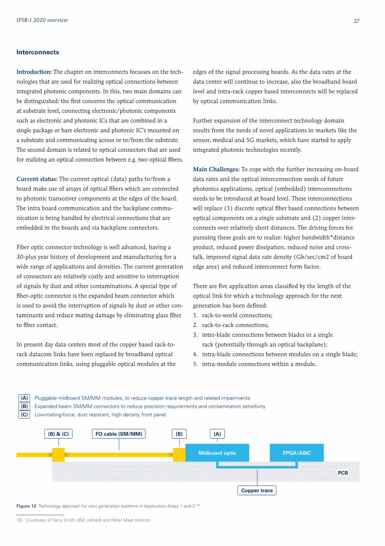
(B) & (C)
Midboard optic FPGA/ASIC
(B) (A)FO cable (SM/MM)
PCB
(A) Pluggable midboard SM/MM modules, to reduce copper trace length and related impairments
(B) Expanded beam SM/MM connectors to reduce precision requirements and contamination sensitivity
(C) Low-mating-force, dust resistant, high density front panel
Figure 12 Technology approach for next generation systems in Application Areas 1 and 2.10)
10) Courtesey of Terry Smith (3M, retired) and Peter Maat (Astron)

28
Copper trace
Midboard optic FPGA/ASIC
(A)FO cable (SM/MM)
PCB
Copper trace
Midboard optic FPGA/ASIC
(A)
(A) Pluggable midboard mount transceivers with fly-over fiber-based media
(B) Optical embedded waveguides including optical interfacing to optical front panel / backplane
(C) Optical backplanes simplifying PCB to PCB optical routing
(D) Expanded beam front panel, backplane, and midplane optical connectors
(D)(B)
PCB
(D)
(C)
Figure 13 Technology approach for next generation systemsin Application Area 3.11)
Copper trace
Optical waveguide
OEIC
EOIC EOIC
(A)
(A) Reflowable electronic/photonic integrated modules to eliminate manual placement of modulesin copper sockets (but still requiring manual coupling of optical conectors)
(B) Interposer on PCB to provide electrical and optical traces connecting separate modules on the same interposer, to isolate modules from PCB reflow process
(C) Optical embedded waveguides incluiding optical interfacing to optical front panel/backplane
(C)
(B)
Figure 14 Technology approach for next generation systemsin Application Area 4.12)
11) Courtesey of Terry Smith (3M, retired) and Peter Maat (Astron)12) Courtesey of Terry Smith (3M, retired) and Peter Maat (Astron)

IPSR-I 2020 overview 29
Additional interconnect advancements in the development
of improved expanded-beam SM connectors are needed to
facilitate high volume deployment of optical interconnects by
overcoming dust contamination, damaged fiber interfaces and
reducing thus preventing costly cable cleaning and inspection
procedures in the field.
To enable wide-scale deployment of substrate-level optical inter-
connects, the following technology gaps and related infrastruc-
ture gaps must be addressed:
• low-mating-force environmentally-robust, contamination-
resistant low-optical-loss connectors for SM systems, e.g.
expanded-beam connectors,
• low manufacturing cost approaches for optical connections
in packaging of PIC devices,
• solder reflow compatible packages and connectors for
integrated optics modules,
• optical coupling component “tool kit” or process design kit
providing low-loss coupling components suited to a wide
variety of PIC designs and foundries, for chip edge, surface
grating and adiabatic evanescent coupling to PICs,
• Low loss substrate-embedded SM waveguides, compatible
with solder reflow, that can eliminate the need to manually
installed fly-over fiber optic cables on board-mount modules
Needs < 5 years
• > 16 fiber SM expanded beam connectors, for cables and modules with manual termination
• SM expanded beam connectors, for optical backplane connectors, frontplane, and midplane applications.
• 24 port module optical interface using pigtail, 1D waveguide array pitch converter
• Module-board attachment via socket
Needs 5-10 years
• > 32 fiber SM expanded beam connectors, for cables and modules with semi-robotic termination
• Low loss optical waveguides for integration in PCBs (<0.2 dB/cm)
• <128 port module optical interface using multicore fiber, 1D waveguide/microlens array, interposer
• Module-board attachment via reflow
Needs > 10 years
• > 64 fiber SM expanded beam connectors, for cables and modules with robotic termination
• >128 port module optical interface using multicore fiber, 2D waveguide/microlens array, interposer

30
Assembly
Introduction: Assembly is the process of bringing together
components, aligning them accurately with respect to one
another and then joining them permanently utilizing a variety
of processes. As compared to typical microelectronic com-
ponents, photonic devices have additional, unique assembly
requirements such as fiber attachments, sub-micron alignment
accuracy, Z axis assembly, particle elimination, etc..
Since packaging and assembly is a large fraction of the cost of
current devices, the focus of this chapter is on reducing these
costs.
Current Status: Many applications require single mode optical
interconnects where alignment, especially of fiber attachments,
are subject to submicron tolerances and stability over the
lifetime of the product.. Generally, rigid materials with high
modulus of elasticity and low thermal coefficient of expan-
sion are best and are used extensively in optical assemblies.
Unfortunately, these materials tend to be expensive, therefore,
much research effort is spent on switching to lower cost materi-
als and lower cost processes to apply these materials.
Another obvious way to avoid assembly cost is to minimize
the number of components to be assembled. That is being
addressed by integration at the platform level in the front-end.
Unfortunately, not all of the functions needed in optical appli-
cations can be integrated monolithically, so separate compo-
nents made with different platform technologies are combined
by what is now called heterogeneous or hybrid integration.
Assembly needs are dictated by the trend to make optical
devices smaller. As mentioned, the inclusion of single mode
components requires sub-micron bond line thickness control
in joints and location tolerances. In addition, sensors not
only comprise PICs but also other specialized components
that impose constraints on the assembly process, restricting
assembly options. Many optical devices incorporate compo-
nents which are sensitive to environmental conditions, e.g. InP,
SiN, GaAs and GaN substrates, polymer based devices. Finally,
optical devices are often 3 dimensional rather than planar. The
net result of these unique more demanding requirements is
that new joining methods utilizing new materials and process
equipment are needed.
Main Challenge: The main challenge in assembly of optical
devices is cost reduction to make them economically viable
in more applications. An important issue in reducing cost is
the relatively small volume (tens of thousands) of photonic
devices that are build, as compared to millions of electronic
devices. This makes the development of new assembly processes
unattractive since the potential revenue from the sale of these
processes is often not large enough to recover their develop-
ment costs.
A current important challenge is reducing the cost of sub-
micron fiber and fiber array alignment. Another challenge is
developing methods to eliminate optical fiber pigtails. Their
inclusion makes manufacturing difficult and expensive.
Alternatives such as waveguides built into substrates and circuit
boards are emerging as an alternative solution. This will require
new assembly processes between components and waveguides
on substrates and in boards.
Developing a robust supply chain for parts with needed charac-
teristics such as fiducials, tight tolerances, smooth, straight flat
edges, good plainarity, consistent lot to lot properties, etc. for
optical products is a challenge.
Increasing volumes of the high mix nature of photonic manu-
facturing calls for a new generation of assembly processes that
is enabled by new equipment which is tooled and programmed
with high flexibility and with high (submicron) precision for a
new product and easy to reset for repeated jobs..
Another need is for the detailed mechanical and optical prop-
erties of the materials used in optical products that are often
not available. Standardizing on those materials and making the
properties available will enable designers to model optical prod-
ucts better and minimize the need to build and test hardware.
Finally standards are needed to minimize development efforts
and enable solutions, once developed, to be used in many
devices. As with other industries, standards will emerge as vol-
ume grows, new devices are introduced and incorporate parts
and processes that are available.

IPSR-I 2020 overview 31
Needs:
< 5 year Needs
• Low cost active alignment for fiber arrays and edge emitters• Assemblying 128 fiber linear arrays to PICs
with < 0.5db loss/fiber for <$0.10/fiber• Supply chains for high tolerance parts; clean edges,
tight dimensional control, lot to lot repeatability, etc.• Die attach methods that provide
submicron thickness tolerances• Supply chains for materials with repeatable
joining dimensions, especially organic compounds with fillers with minimal lot-to-lot variation
• Methods to protect water and oxygen sensitive materials (InP), surfaces and components from the environment
5-10 year Needs
• Methods to build optical functions in the Z direction with sub micron accuracy and optical quality surfaces.=
• 3D optical devices utilizing software that incorporates mechanical, electrical and thermal requirements
• Methods to optically connect large fiber bundles (64 x 64 = 4096 fiber) to PICs.=
• Optical electronic platform that will serve many applications with minimal customization
• Minimizing variation in final dimensions by methods without joining materials
Needs > 10 years
• Sub micron alignment of optical beams to metamaterials enabling materials to perform highly specific functions
• 0.01micron dimensional tolerances to implement new functions
• A production method of fabricating optical waveguides in-situ to transmit light with low loss from a source to a sink. i.e. optical “wire bonding”
• Assembly methods to enable wavelength selection to 1 part in 106 and extracting signals that are 60+db lower in strength than overlapping signals.
• Developing assembly tools that have nanometer resolution.
These needs assume:
1. The cost for optical functions decreases >10%/yr.
2. Optical devices become smaller limited
only by optical wavelengths.
3. Tolerances required become far smaller
than the wavelength of light.
4. The most challenging requirements result from
single mode and low level optical signals.
5. Data Communication rates continue growing,
meaning per lane and through the internet.
6. Meta Materials arise as an enabler.
7. Non-linear optical phenomena come into
use to provide additional functions.
8. 3D printing of single mode optical devices and
optical quality surfaces becomes viable.
9. Monolithic integration capability grows to enable
inclusion of direct bandgap materials.
10. Photonic Integrated Circuits are monolithically
integrated with electronic functions.
11. The number of optical devices built
and sold grows at ~25%/yr.

32
Testing
Introduction: In the electronic integrated circuit (IC) industry,
testing has become a mature process supported by practices and
equipment that have been heavily optimized to drive down the
cost and time spent on IC testing. In contrast, development of
similar methods and tools for the PIC-community is still at an
early stage and the extra complexity that arises from having to
measure both in the optical and the electrical domain poses
many challenges.
The term PIC refers to an immensely diverse fi eld of different
implementations where we need to consider different
(1) materials (InP, GaAs, Si, polymer, SiN, glass), (2) integration
schemes (monolithic, hybrid, etc.), (3) packaging (hermetic,
non-hermetic, material) and (4) optical couplers (gratings, edge,
mirrors coupled to single fi bers, fi ber arrays, lensed fi bers, etc.).
Main challenges: This leads to a fi rst key development area:
standardization of test metrics. New standardized testing
methodologies and qualifi cation parameters need to be devised
that apply to all technologies, types of packages, and all relevant
environmental conditions – leading to a truly platform-agnostic
test solution.
A second key area is to consolidate the design and test work
fl ow. A four-step method is proposed to enhance collabo-
ration between designers, fab engineers and test engineers.
Variations in dimensional and physical properties of materials
and modules need to be understood and taken into account
during design. This permits engineers to predict the infl uence
of process variations on measurement results and allows them
to design dedicated and improved test structures up front. By
repeating these steps in combination with a careful analysis
of the stored data, the number of devices to be measured and
tracked can be reduced and the functional yield is expected to
increase.
This targeted reduction in number of devices brings us to a
third key area: test time reduction. There is a clear need for fully
automated test systems. On the one hand this includes inline
and where possible in-situ process testing at wafer level such as
critical-dimension (CD) monitoring, defects counting, ellip-
sometry, etc. On the other hand, this includes the (out-of-line)
automatic functional testing at wafer, bar/die and module level.
For the functional test a massively parallel test approach is
envisaged in order to bring down measurement time and cost.
Design Front-end foundry Systemintegration
Back-end foundry
Test template
Test script
Simplified test
Modelling & simulation
DE
SIG
N F
OR
TE
ST
Design for test
DATA
Design for test
DATA
Design for test
DATA
Design for test
DATA
Design for test
DATA
Design for test
DATA
Electrical only!
Electro-optical
Automated
SPC
Machinelearning
ON
-WAT
ER
TE
ST Automated
Electro-optical
SPC
BA
R T
EST
ING Pre-package
Automated
SPC
User defined
Functional
DIE
TE
STIN
G System level
Performance
Stress test
Environmental
MO
DU
LE T
EST
ING
PR
OD
UC
T
Figure 15 Test framework for data fl ow and exchange across production chain from a design to product (www.openepda.org)13)
13) Courtesey of Peter Sylwester Latkowski, Photonic Integration Technology Centre (PITC)

IPSR-I 2020 overview 33
More specifi cally for wafer-level testing, this highly parallel test
approach can be enabled by scalable and modular test equip-
ment and an increase in the number of electrical and optical
input-output (IO) ports per test site. For electrical measurement
instrumentation this modular approach is already quite well
established; for optical instruments this is an emerging concept.
In order to increase the number of optical IOs per test site from
10s to 100s of couplers in the next 10 years, multi-core fi bers or
fi ber arrays will have to be used in combination with an optical
interposer to reduce the pitch of optical IOs. Measuring optical
signals indirectly using on-chip photodiodes is another interest-
ing option to eliminate the need for optical alignment.
In contrast to SiPh, InP- and GaAs-chips often require bar /
die level testing. Main reason is that often waveguides irradiate
from cleaved facets at the side of the chips covered with ultra-
low antirefl ection coating. In the future the target will be to
replace cleaved facets by on-wafer etched facets and to replace
facet coating by on-wafer coating. Then most of the bar / die
testing can be avoided and wafer level testing can be used. In
case of SiN devices it is expected that even in future die testing
will remain playing an important role.
In addition to functional testing, also the area of reliability /
lifetime testing needs to be addressed. To date commercially
available life time testing equipment is mainly based on fi ber
attached mounted single dies or mounted single devices that are
being tested with free space measurement setups (e.g. laser life-
time measurements using large area photodiodes). Such inves-
tigations are expensive. Performing these tests at wafer level,
simultaneously on multiple dies is an option to be investigated.
This will also require developments in terms instrumentation,
e.g. high-power laser sources for accelerated lifetime testing.
The overall lifetime test issues of photonic components and
products is addressed. Its emphasis is on silicon wafers and dies
with photonic functionality and assemblies and products that
include these devices. Systems in Package (SiP) assemblies and
systems are addressed to the extent viable given the diversity of
test needs that are specifi c to applications. As shown by the fi g-
ure below, the test issues for wafers, die, SiPs, and fi nal products
need to be addressed at the Design, Qualifi cation, Validation,
Production, and In-Use stages of product life cycles. Current and
anticipated optical parameters to be tested are considered along
with the test access issue at each stage of the product life cycle.
In useTo provide notificationof deterioratingperformance
• Variation over time of key parameters
• Output signal quality
• Power consumed• Temperature rise• SNR/eye diagram
ProductionTo monitorongoing quality
Measure key parameters, often sampling:• Output signal
quality• Power consumed• Temperature rise• Dimensions to
spec• Acceptable eye
diagram
ValidationTo ensure themanufacturingprocess producesconsistent quality
• Output signal quality
• Power consumed• Temperature rise• Dimensions to
spec• Acceptable eye
diagram & yield• Evaluate lot-to-lot
variation
QualificationTo ensure the product meetsrequirements
• Environtental extremes OK
• Power/Voltage variation impact OK
• Bit error rate OK• Input signal
extremes• Output signal
extremes• Attenuation,
signal-to-noise, jitter, skew OK
• Evaluate multiple lots
• Temperature rise• Mechanical
dimensions• Perform over
temperature range• Extrapolated
performance meets specification
Design &developmentTo evaluatevarious designs
As determined by Engineering. Typically:• HAST• Margin checks• Temperature
dependence• Component
tolerance impact
STA
GE
OF
LIFE
CYC
LETY
PIC
AL
OP
TIC
AL
TE
ST
S
LIFE CYCLE FLOW
Figure 16 Test needs during an optical product life cycle14) 14) Courtesey of Richard Otte, Promex Industries

34
Telecommunications test equipment, components, and methods
were and are being adopted for optical testing of products used
for non-long haul applications. The traditional methods are
being extended and new methods developed to address test needs
for photonic wafers, photonic integrated circuits, and SiP that
utilize optics and complete systems. Utilizing these extended
methods requires optical probing of both wafers and dies com-
bined with electrical probing resulting in a series of mechanical
issues. The inclusion of optical probing, especially single mode
probing, requires gratings or other access points on wafers. For
individual die, dual mode (electrical and optical) probing is
especially difficult due to the small size of die and difficulty of
holding and locating probes accurately. At the SiP level, the prob-
lems are easier because the device is larger, not as fragile, and is
often designed to facilitate dual media probing. The wafer, die,
and SiP probe fixtures tend to be expensive due to the complexity
and accuracy required. System level test access is usually easier
because at that level, electrical interfaces and optical connectors
are included as part of the device under test (DUT).
In addition to probe access, optical test methods to simul-
taneously characterize and compare multiple optical lanes,
channels and/or ports at the same time are needed. One need
is comparative simultaneous testing of multiple signals from
arrays of ribbon fibers, waveguides, sources or detectors for
optical skew, jitter, etc. A related need is to simultaneously
evaluate optical signals multiplexed on one fiber or waveguide.
Applications with arrays exceeding 256 ports (fibers or wave-
guides) or >256 multiplexed wavelengths are forecast in the
next ten years.
In addition to the standard telecom optical parameters such as
power, wavelength, attenuation, jitter, signal-to-noise ration
(SNR), etc., emerging applications utilize virtually every param-
eter that light can have, potentially requiring the extension
of test capability in multiple dimensions such as polarization,
phase noise, amplitude noise spatial modes, multiple fiber
cores, etc. While these emerging needs are potentially very
broad, the near-term emerging needs seem most likely to be
extensions of data communications needs.
Optical communication applications are likely to utilize 650
nm to 1700 nm wavelengths, multiplexed wavelength spacing
down of 25 GHz, detector responsivity of ~1 A/W, receiver
sensitivity as great as -45 dBm, power levels of 1 Watt or less,
symbol rates of 100 Gbaud per lane, modulation schemes

IPSR-I 2020 overview 35
utilizing up to 10 bits per symbol, polarization multiplexing,
BERs of 10-12, etc. Over time, these parameters will improve
so test capabilities will need to stay ahead of them. Data rates
as high as 500 Tbps per fiber are likely to emerge in the next
10- 15 years.
Sensor applications are likely to grow significantly in the next
10-15 years as remote fiber sensors are integrated into physical
structures for strain and temperature sensing, and as chip-
level chemical and biological sensors are introduced into the
marketplace. While these applications will still require the same
baseline test solutions as is required for telecom and datacom,
the functional tests are likely to be quite different.
Quantum technologies add yet a different dimension for
testing. The use of single photon and entangled-photon sources
and circuits will yield its own complexity. There is currently no
standardized test equipment for these applications; however,
testing methods are currently being developed with University,
Government, and Industrial research labs and will require
consideration in future editions of this document.
Regardless of application, the principles of design for test
remain the same: The use of optical test access points, Built-In
Self-Test (BIST), redundancy for self-repair, re-purpose and
prognostics to report changes and deterioration during oper-
ation over the life cycle of optical products are desirable and
of value in an increasing number of applications. These tests
should be considered for inclusion not only in designs, but also
in software design tools as well.
Needs:
< 5 year Needs
• Photonic testing moves from slow custom solutions to faster application agnostic automated test solutions
• Test of ~20 optical ports per chip with IO pitch <= 127um located in a linear array
• Insertion loss during test < 20 dB• Wafer probe test times per chip 5-20
minutes (single site testing)”
5-10 year Needs
• Viable test methods emerge for hybrid integration of photonic device
• Test of ~ 100 optical ports per chip with IO pitch <= 50um aligning with multicore fiber geometries
• Insertion loss during test < 10 dB• Wafer probe test times per chip 5-10
minutes (2-4 site testing)”
Needs > 10 years
• On chip self-testing techniques – Test while operating• Test of ~500 optical ports per chip with IO pitch
<= 20um supporting flip-chip technology• Insertion loss during test < 5 dB• Wafer probe test times per chip 2-5
minutes (4-8 site testing)”

36
Chapter 4
Product and design

IPSR-I 2020 overview 37
Bringing down the cost per function in integrated photonics
can be done in three ways:
• reducing the cost of prototyping (development engineering),
• reducing the cost of production processes
(manufacturing engineering) and
• creating economies of scale and associated
infrastructure by ramping up volumes.
The latter one is a paradox on its own because the volumes to
reduce cost can’t be reached without cost reduction. However,
the economies of scale are a leverage on the efforts in develop-
ment engineering (high-mix applications) and manufacturing
engineering (low-mix applications).
Development engineering
Manufacturing engineering
InterconnectsPackaging Substrates
Front-endAssembly Testing
Design for manufacturing ofphotonic integrated circuits & modules
Figure 17 Technologies related to development and manufacturing engineering
TestPackagingAssemblyLithographyOther front-endGrowth
FRONT – END FOUNDRY PICs
COST
1% 8% 8% 24% 30% 29%
BACK – END FOUNDRY PICs
Figure 18 Break-out of the cost for a PIC module15)
In the front-end and back-end chapters the different technolo-
gies have been discussed that are required to develop and man-
ufacture PICs. Both the testing of wafers, (packaged) dies and
modules, and the (Electronic-Photonic) all overlap the previ-
ously mentioned chapters and intersect with these technologies.
As has been pointed out in previous sections, the main cost
of a module originates from the back-end processing. When
designing a PIC module costs of all relevant technologies and
production steps need to be taken into account, i.e. the front-
end platforms, packaging and assembly.
Next to starting with the full designing for the module in mind,
the reduction of the number of components that need to be
assembled can generate large cost savings. This is achieved by
integrating more functions monolithically. The fi rst improve-
ment will be to merge both actives and passives via hybrid
system in packages, for example with PCB’s, interposers and
effi cient wirebonding & optical connections. The second step
is to have wafer-scale heterogeneous electronic-optic (i.e.
CMOS-SiPh or InP-CMOS) or (active)optic-(passive)optic (i.e.
InP-SiPh) integration. The end goal is to achieve full monolithic
integration of actives, passives and electronic, some of the ideas
include methods to give silicon the properties of actives or have
full InP wafers.
15) Process-Based Cost Modeling of Photonics Manufacture: The Cost Competitiveness of Monolithic Integration of a 1550-nm DFB Laser and an Electroabsorptive Modulator on an InP Platform” in IEEE Journal of Lightwave Technology, Vol. 24, No. 8, 2006.

38
EPDA
Introduction: The electronic design community is large and
has had years of experience with ever improving design tools.
The photonic design community is relatively small and until
recently used “homegrown” design tools or commercial tools
developed for experts and researchers. To tap into the larger
traditional electronic IC design community, using Electronic
Design Automation (EDA) solutions, the goal should be to
mimic the function of existing EDA platforms when incorpo-
rating the photonics aspect resulting in an Electronic Photonic
Design Automation (EPDA) environment.
The introduction of Process Design Kits (PDKs) in 2008
together with the Multi Project Wafer runs has largely sup-
ported the more widely application of PIC technology in
domains outside the traditional telecom space and acceler-
ated the transition from academic research into commercial
manufacturing.
Main Challenges: However, to further develop this technology,
the maturity of the PDKs needs to be improved. This requires
an orchestrated effort between foundries at one side, developing
more capable and stable processes and implementing more
design, process and test information in PDKs, and software
vendors at the other side, improving the tools and flows to be
able to use more information from the foundries to support
design for manufacturing, yield and cost.

IPSR-I 2020 overview 39
Sensors
Introduction: Micro-fluidic and biosensors based on integrated
photonics will enable a variety of applications to generate
information that either cannot be obtained otherwise or only at
high costs. Micro-fluidic sensors cover a broad range of markets
ranging from consumer medical and food markets to defense
and industrial markets. There are some technical barriers that
affect all the industries, mainly related to the requirement of
lowCost, Size, Weight and Power consumption (CSWaP).
This requirement of low-CSWaP ultimately drives the technol-
ogy towards highly integrated photonic circuits which extend
well beyond the conventional solutions based on discrete
components. The integration of active components such as light
sources, optical detectors and optical modulator structures onto
passive SiPh or SiN devices is enabling the market to realize
highly integrated-low CSWaP microfluidic sensors.
Current status: Recently advances in optical components
operating in the UV and IR regimes enable high sensitivity sen-
sors. The realization of low CSWaP designs, fast New Product
Introduction (NPI) cycles and custom wavelength tunability
of integrated photonic packages in the IR, UV range will allow
quick time to market of microfluidic and biosensors.
Main challenges: There are many challenges related to the
realization of low CSWaP microfluidic and biosensors. These
challenges include the development of appropriate sensor archi-
tectures, design of the photonic sensing element, the develop-
ment of the microfluidic assembly and the final packaging of
the device.
Sensor Architecture challenges relate to the integration of wave-
length specific features and active devices into a low CSWaP
package. Sources and detectors must be integrated while main-
taining optical specifications over a variety of environments.
Improvement of wavelength specific passive devices includes
ring resonators, MZI interferometers, and spiral waveguides is
required.
Challenges pertaining to the photonic sensing elements are
specifically addressing the photonic design kit improvements
which are essential for a quick design turn around, interface
definitions including input, output, and interface standards
as well as overall specifications and testability of the sensing
elements arrangement.
Sensor architecture challenges also include microfluidic specific
elements such as integration and design of different materials.
The microfluidic assembly challenges are outlined around the
design and manufacturability of the designs. Specifications, key
interface development, and manufacturing planning all present
various problems requiring further technology development.
While significant development and maturity have been demon-
strated for various aspects of active component integration at
various wavelengths, the current manufacturing capabilities
haven’t addressed the market challenges presented for photonic
sensors. In Manufacturing, stamper development, disk mold-
ing, punching, and other fabrication methods present barriers
to entry and present key opportunities for improvement.
Needs:
Needs < 5 years
• Low CSWaP sensors• PICs with integrated Ge detectors• Interposer-based lasers (1.3um to 1.5um)• Automated AWG in mature PDKs
Needs 5-10 years
• Wider spectral bandwidth sources• Integrated detectors• Short wavelength Sources on PICs• Flourescence detection (VIS)• Mid-IR, Long-IR Detectors• Monolithic on-chip lasers• 3-5um spectrometers
Needs > 10 years
• Low cost ultra-small packaging• Monolithic tunable sources on PICs• Multiple wavelength passive waveguides• Monolithic/ hybrid intergation of multiple light sources • Integrated spectroscopy, RI and
flourescence sensors in PICs.

40
RF Photonics
Introduction: The RF Photonics chapter covers the integrated
electronic-photonic technology applications that have been
identified to be particularly important to meet high speed
analog communication needs over optical fiber links. Important
functionalities include filtering and delays - and frequency
control in signal generation, distribution, processing and
measurement.
Current situation: In particular the need for high-speed,
low-latency data transfer is driving the need for integrated
photonic components. The enabling technologies include:
• Heterogeneous packaging (Through-Silicon Vias
(TSV) for stacked chips and silicon interposers),
• System in Package (SiP) and Package on Package (PoP),
• Integrated silicon photonics systems,
• Lower loss interconnect (low-loss laminates in
printed circuit boards and packages), and
• More efficient power conversion (wide band-gap materials).
Challenges:
Component Current general performance
Future performance goals
Source 250 mW @ 1550 nm; 10 -15% maximum efficiency
0.5 W to 1 W @ 1550 nm; 20- 30% maxi-mum efficiency
Modulator 100 GHz bandwidth; Vp in the range of 3- 10 V; 2-3 dB loss
100 GHz bandwidth; Vp in the range of 1-5 V; 1-2 dB loss
Filter Bandwidths of 50 MHz -5 GHz; 1-5 poles; Q > 1,000,000; high insertion loss per pole; low power handling (PIC)
Bandwidths of 10 MHz to multiple GHz; insertion loss <1 dB per pole; >3-5 poles; Q > 10,000,000; power handling of 100 mW
Photodetector 100 GHz bandwidth; low power handling of a few milliwatts
100 GHz bandwidth; 500 mW power handling
Table 1 Challenges in RF photonics

IPSR-I 2020 overview 41
Cost emulators
We limit our analysis to only the packaging of the optical
devices into a module. The costs of components are taken
as inputs and are not taken into consideration. Although we
carry out sensitivities to understand the potential implication
of various levels of component costs, the reader should view
this analysis as incomplete. Although incomplete, this chapter
serves to demonstrate the potential for detailed process-based
cost analysis to critical photonics questions.
Preliminary results suggest that:
• monolithic integration has the potential to signifi cantly
lower packaging cost for both high and low volume
production;
• the key cost savings opportunity for integrating in the near
term derives from avoiding the expense of assembling and
packaging the interposer layer;
Hybridpackaging
Monolithic w/Hybrid laserpackaging
Fullymonolithicpackaging
No
rmal
ized
co
st v
alu
e
0
0,5
1,0
Component $/pcOther mat. $/pcLabor $/pcEquipment $/pcMask & tool $/pcOther $/pc
Figure 19 Baseline model result. a) Modeled unit cost versus production volume16)
5 50 100 1000Thousands
No
rmal
ized
co
st v
alu
e
0
1
2
3
Fullt monolithic packagingMonolithic w/hybrid laser packagingHybrid packaging
Figure 19 Baseline model result. b) Cost breakdown by cost element for the three different levels op integration16)
Integration has signifi cant cost advantages even if optical chip
yields were to fall well below baseline modeled values.
16) Courtesey of Randolph Kirchain, Elsa Olivetti, Wei Yu (MIT)

42

IPSR-I 2020 overview 43

The objective of the IPSR-I is to establish and sustain a trust based global network of Industrial and R&D partners, who are working together on defining and creating future Photonic Integrated Circuit (PIC) and Systems Technology and Systems Requirements. They jointly enable faster technology and application developments in this emerging business, guided by an up-to-date technology and application roadmap for future developments.
The IPSR-I is the result of the efforts of more than 250 experts from all over the world, working in the field of integrated photonic technologies and their applications. It gives an overview of the current status of technologies and of applications in which integrated photonic components are used. Above all it describes the trends, expectations
and needs for technology and application development in the near (0-5 years), intermediate (5-10 years) and far (10-20 years) future.
The roadmap document is a merger between previously separately produced roadmaps: the IPSR by AIM Photonics from the USA and the WTMF by Photon Delta from Europe. Apart from merging both roadmaps, it has obtained a thorough update based on 32 workshops and countless online working group meetings. However, the IPSR-I is a living document that is continuously updated. The chapters need enrichment with technological and application developments in their respective fields. A continuous call is open for contributions by experts in the various technology and application fields to update the IPSR-I.
IPSR-I 2020 overview
BerenschotPowered by