iot applications and design guide ebook (mwj) | qorvo
TRANSCRIPT

IoT Applications and Design Guide
E - BO O K
OCTOBER 2018
S P O N S O R E D B Y
2
Table of Contents
3 Introduction Patrick Hindle Microwave Journal, Editor
11 Simulation Speeds NB-IoT Product Development Takao Inoue and David Vye AWR Group, NI, El Segundo, Calif.
16 Antenna Technologies for the Future Pat Hindle Editor, Microwave Journal
4 Addressing The Challenges Facing IoT Adoption Kailash Narayanan Keysight Technologies, Santa Rosa, Calif.
7 Evolution of The IoT as a Service Cees Links Qorvo
22 Antenna Design Methodology for Smartwatch Applications Phil Lindsey ARSI LLC, Atlanta, Kan C. J. Reddy Altair Engineering Inc., Hampton, Va.
27 Distributed Wi-Fi: How a Pod in Every Room Enables Connected Smart Homes Cees Links Qorvo
3
Introduction
Pat Hindle, Microwave Journal Editor
IoT Applications and Design Guide
With the projected number of IoT devices to be 20 to 30 billion by 2020 and about 50 billion in 2025, there is no doubt about the importance of wireless devices for this market. The Industrial IoT (IIoT) is expected to be the largest part of the market initially so especially important to device manufacturers. IIoT addresses wide deployments of devices from smart cities to industry 4.0 advanced factories so encompasses many applications. Connected and autonomous vehicles are a very active area and will probably start with ride services and transportation of goods followed by personal automobiles. Another large sector is the smart home where security cameras, consumer devices and smart appliances are growing quickly. There also promises to be significant growth in the medical sector with connected equipment and even robotic surgery on the horizon. The future of IoT is open to our imagination as 5G rolls out and other IoT specific networks are deployed.
This eBook takes a look at the emergence of IoT and design of devices for this market. The first couple of articles take a look at the overall IoT market challenges and trends for smart home services. One big challenge for the industry is designing devices with low power designs and antennas that provide good performance in the space needed to fit into small areas contained within the device. So the next article addresses rapid product development of NB-IoT devices with simulation followed by a couple of articles addressing antenna design and new antenna technologies. There are some very interesting new antenna technologies under development that could enable even better performance for IoT applications ranging from medical to home to industrial applications. The eBook concludes with an article addressing design for IEEE 802.11ax for distributed WiFi in the home.
This eBook should help designers learn about the IoT market and design challenges facing the industry. The simulation and design techniques covered will help enable better designs and performance for wireless devices in addressing the IoT market. JFW and Qorvo have sponsored this eBook and offer many devices that will help address designs in this market so thank them for bringing this complimentary collection of articles to our readers.

Addressing The Challenges Facing IoT AdoptionKailash NarayananKeysight Technologies, Santa Rosa, Calif.
The Internet of Things (IoT) phenom-enon—ubiquitous connected things providing key physical data and further processing of that data in the cloud to
deliver business insights— presents a huge op-portunity for many players in electronics and software, including chipset vendors, device de-velopers, OEMs, manufacturers, equipment ven-dors, network operators and end-to-end solu-tions providers. Many companies are organizing themselves to focus on IoT and the connectivity of their future products.
CHALLENGESFor the IoT industry to thrive, three items are
crucial: a viable business model, a robust con-nectivity topology and reliable devices. This arti-cle discusses these, focusing on the design chal-lenges that must be overcome to make reliable devices. Challenges vary depending on the IoT application. While cost is a major factor in con-sumer applications (e.g., wearables and home automation), industrial IoT applications (e.g., smart grids, connected cars and transportation) require unfailing reliability, longevity, security and the ability to operate devices with little or no human intervention.
The Business ModelEnd-to-end solution providers operating in
vertical industries and delivering services using
cloud analytics will be the most successful at monetizing a large portion of the value in IoT. Low power, wide area (LPWA) IoT technolo-gies open up possibilities for service providers. Knowing the location of pets and vehicles, track-ing valuable personal belongings, monitoring utility usage, obtaining real-time data on the health of crops and livestock, employee fatigue and machine status are useful for individuals and businesses.
A typical smartphone contract delivers rough-ly five cents per MB of data. Assuming an IoT application uses 100 KB per month, and a user is willing to pay a modest 10 cents per month for these new IoT applications, that’s already better business for an operator. Delivering $1 per MB is 20x more revenue than a typical smartphone contract for the same amount of data consump-tion. While many IoT applications may attract modest revenue, some can attract more than $10 per month. For little burden on the existing communication infrastructure, operators have the potential to open up a significant source of new revenue using LPWA technologies. Clearly, it is important to understand the value chain and business model for the IoT application.
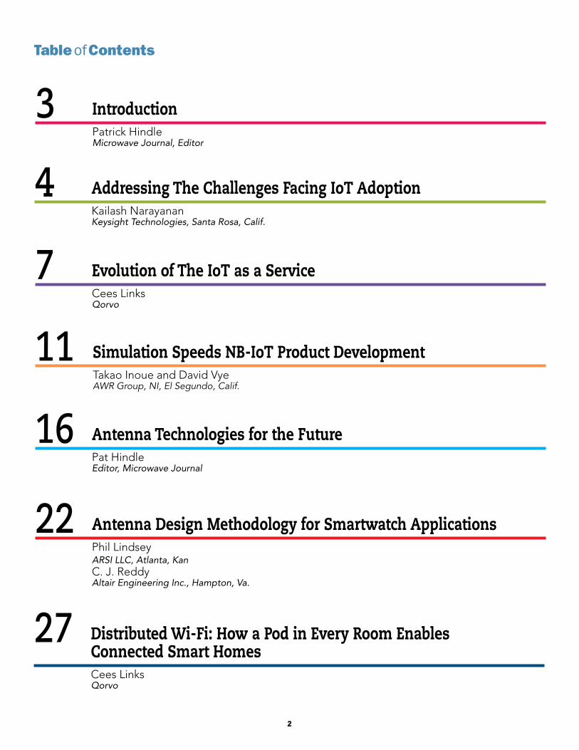
Connectivity TopologyFigure 1 shows a simple IoT network model,
consisting of a device layer containing “things” with sensors and actuators that capture or initi-
WWW.MWJOURNAL.COM/ARTICLES/276904
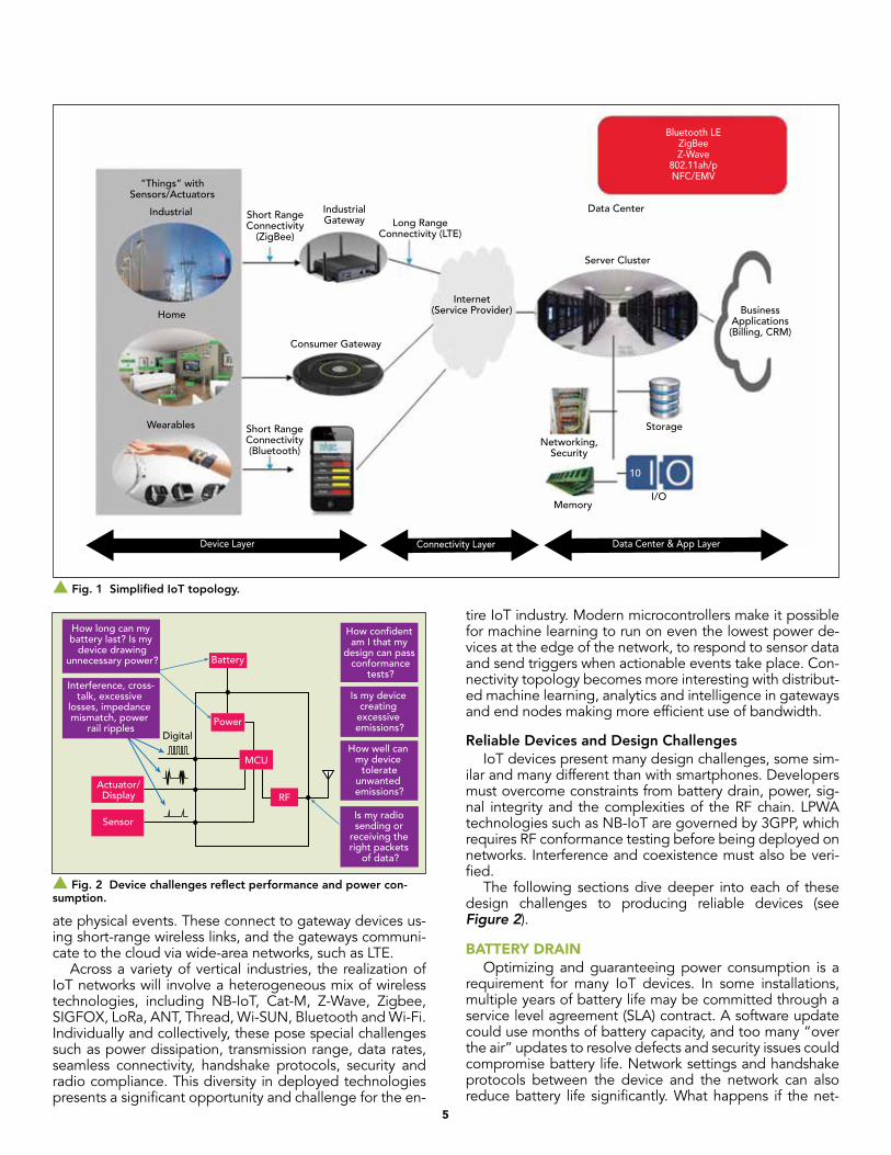
5
ate physical events. These connect to gateway devices us-ing short-range wireless links, and the gateways communi-cate to the cloud via wide-area networks, such as LTE.
Across a variety of vertical industries, the realization of IoT networks will involve a heterogeneous mix of wireless technologies, including NB-IoT, Cat-M, Z-Wave, Zigbee, SIGFOX, LoRa, ANT, Thread, Wi-SUN, Bluetooth and Wi-Fi. Individually and collectively, these pose special challenges such as power dissipation, transmission range, data rates, seamless connectivity, handshake protocols, security and radio compliance. This diversity in deployed technologies presents a significant opportunity and challenge for the en-
tire IoT industry. Modern microcontrollers make it possible for machine learning to run on even the lowest power de-vices at the edge of the network, to respond to sensor data and send triggers when actionable events take place. Con-nectivity topology becomes more interesting with distribut-ed machine learning, analytics and intelligence in gateways and end nodes making more efficient use of bandwidth.
Reliable Devices and Design ChallengesIoT devices present many design challenges, some sim-
ilar and many different than with smartphones. Developers must overcome constraints from battery drain, power, sig-nal integrity and the complexities of the RF chain. LPWA technologies such as NB-IoT are governed by 3GPP, which requires RF conformance testing before being deployed on networks. Interference and coexistence must also be veri-fied.
The following sections dive deeper into each of these design challenges to producing reliable devices (see Figure 2).
BATTERY DRAINOptimizing and guaranteeing power consumption is a
requirement for many IoT devices. In some installations, multiple years of battery life may be committed through a service level agreement (SLA) contract. A software update could use months of battery capacity, and too many “over the air” updates to resolve defects and security issues could compromise battery life. Network settings and handshake protocols between the device and the network can also reduce battery life significantly. What happens if the net-
s Fig. 2 Device challenges reflect performance and power con-sumption.
Digital
How con�dent am I that my
design can pass conformance
tests?
How long can my battery last? Is my
device drawingunnecessary power?
Interference, cross-talk, excessive
losses, impedance mismatch, power
rail ripples
Actuator/Display
Sensor
Battery
Power
MCU
RF
How well can my device
tolerateunwanted emissions?
Is my radio sending or
receiving the right packets
of data?
Is my device creating
excessive emissions?
s Fig. 1 Simplified IoT topology.
Long RangeConnectivity (LTE)
BusinessApplications(Billing, CRM)
Storage
I/O
10
Memory
Networking,Security
Server Cluster
Data CenterIndustrialGateway
Internet(Service Provider)
Short RangeConnectivity
(ZigBee)
“Things” withSensors/Actuators
Industrial
Home
Wearables Short RangeConnectivity(Bluetooth)
Bluetooth LEZigBeeZ-Wave
802.11ah/pNFC/EMV
Device Layer Connectivity Layer Data Center & App Layer
Consumer Gateway
6
traces get closer together and supply voltages are lowered. Common signal integrity issues that can degrade over-
all system performance include reflections, excessive loss-es, crosstalk, distortion and power supply noise. Power integrity speaks to how effectively the power is converted and delivered from the power source to the load within the device. With the drive toward low power electronics, DC supply voltages and tolerances have been reduced, some from ±5 percent to ±1 percent. Ripple, noise and transients riding on the output power rails can adversely impact the clock and accuracy of digital data. Designers need a power integrity solution that can measure these low DC voltages with high accuracy.
CO-EXISTENCE AND CONFORMANCEIoT devices may be integrated into products and gate-
ways that include a variety of different standards operating over a range of frequencies. Each radio and device type will need to meet a specific set of downstream acceptance tests. Cellular devices need to pass certification tests from standards bodies, and many operators have their own ac-ceptance test plans. All devices must pass regulatory test-ing that depends on frequency band and region. Many system integrators run their own acceptance tests to select modules in their systems. So designers need to ensure that interference and intermodulation effects are anticipated, understood and tested.
SECURITYIoT devices at the edge of the network increase the se-
curity vulnerability of networks. Yet devices don’t have the needed resources to host sophisticated security protocols. The capability for remote software updates needs to be designed into the device to allow for security updates, which has implications on battery life. Authentication and cyber security features need to be tested and upgrade-able. The most secure development approaches available today are likely to be compromised in the coming years, so security patches should be anticipated. In the future, security will likely be built into these devices.
CONCLUSIONIoT is likely to be a significant enabler of many disruptive
business models and market efficiencies. Recall how the in-ternet and players like Amazon, eBay and Uber have and are transforming markets. Peer-to-peer banking, personal-ized car insurance, personalized health insurance and crowd-sourced businesses are emerging. IoT devices for ordering convenience will lead to more services on top of products. These new business models and services rely on networks of sensors and actuators, linked by radio and connected to the cloud for data analytics. For these big connected sensor systems to work well, even the smallest of components must be secure, stable and reliable.n
Kailash Narayanan is vice president and general manager at Keysight Technologies, where he leads the wireless device business and is responsible for product and solution development, marketing and delivery to the wireless device ecosystem. His current focus is 5G and IoT. He received a master’s in electrical engineer-ing from the University of Illinois, Chicago and an MBA from Walden University.
work is down? Does the device search re-peatedly for the net-work and drain the battery?
For IoT devices, the active state —when the device is transmitting or re-ceiving data—is very short compared to
idle and standby states. Measuring the current consump-tion is key to understanding and optimizing the power consumption. Figure 3 illustrates the different device op-erating states and the resulting current drain, likely a ratio of 1:1,000,000, from sub-µA to 100 mA. For example, in transmit, Bluetooth low energy transmitters use tens of mA compared to a few A for GSM transmitters. The majority of the time, devices are in idle mode, drawing from tens to hundreds of nA up to hundreds of µA.
Because IoT devices have very low duty cycles, a com-mon way to lower the total current drain is to design the system so the device has a very short active state followed by periods of relatively low activity or no activity. The chal-lenge in verifying the likely battery life is to accurately mea-sure the dynamic current drain across the different operat-ing modes over a period of time and with a single view that provides a complete and detailed analysis.
RADIO FORMATSWith many types of devices deployed in consumer and
industrial applications (e.g., smart grid, smart energy, smart factories and smart homes), many IoT formats are being deployed and many operate in the same spectrum (e.g., Wi-Fi, Bluetooth and Zigbee). These environments will af-fect multi-radio interference (co-channel or adjacent chan-nel), transmission range and speed, and interoperability. All must be considered.
NB-IoT, Cat-M and other LPWA technologies use narrow bandwidths to connect to IoT/M2M devices, resulting in lower data rates and low power. Thread is a secure wireless mesh network for home and connected products; based on the 802.15.4 physical and MAC layers it enables the gate-way to easily control connection to the cloud. Bluetooth has been the most commonly used format for consumer electronics and is often used around the smartphone and near field communication (NFC) for payments. Wi-Fi is a foundational technology that is used wherever possible. LPWA formats like LoRa and SIGFOX are opening up new applications. Many other technologies such as Zigbee, ANT and Z-Wave are being used for home automation.
With all these technologies, the radio design has to be optimized for data rates and sensitivity. Good RF transceiver and antenna design are needed to achieve deep in-build-ing coverage, as making a receiver work hard to decode a weak signal further reduces battery life.
POWER AND SIGNAL INTEGRITYThe increased demand for expanded functionality in a
small form factor drives the need for higher density, lower power and compact circuit design. Maintaining signal in-tegrity and power integrity becomes more challenging as
s Fig. 3 Device current consumption varies with operating mode.
100 mA
Sub-µA
ActiveCurrent Pulses
Idle CurrentPulses
SleepCurrent
I
t
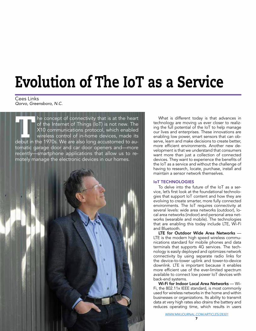
Evolution of The IoT as a ServiceCees LinksQorvo, Greensboro, N.C.
T he concept of connectivity that is at the heart of the Internet of Things (IoT) is not new. The X10 communications protocol, which enabled wireless control of in-home devices, made its
debut in the 1970s. We are also long accustomed to au-tomatic garage door and car door openers and—more recently—smartphone applications that allow us to re-motely manage the electronic devices in our homes.
What is different today is that advances in technology are moving us ever closer to realiz-ing the full potential of the IoT to help manage our lives and enterprises. These innovations are enabling low power, smart sensors that can ob-serve, learn and make decisions to create better, more efficient environments. Another new de-velopment is that we understand that consumers want more than just a collection of connected devices. They want to experience the benefits of the IoT as a service and without the challenge of having to research, locate, purchase, install and maintain a sensor network themselves.
IoT TECHNOLOGIESTo delve into the future of the IoT as a ser-
vice, let’s first look at the foundational technolo-gies that support IoT content and how they are evolving to create smarter, more fully connected environments. The IoT requires connectivity at several levels: wide area networks (outdoor), lo-cal area networks (indoor) and personal area net-works (wearable and mobile). The technologies that are enabling this today include LTE, Wi-Fi and Bluetooth.
LTE for Outdoor Wide Area Networks — LTE is the modern high speed wireless commu-nications standard for mobile phones and data terminals that supports 4G services. The tech-nology is easily deployed and optimizes network connectivity by using separate radio links for the device-to-tower uplink and tower-to-device downlink. LTE is important because it enables more efficient use of the ever-limited spectrum available to connect low power IoT devices with back-end systems.
Wi-Fi for Indoor Local Area Networks — Wi-Fi, the 802.11x IEEE standard, is most commonly used for wireless networks in the home and within businesses or organizations. Its ability to transmit data at very high rates also drains the battery and reduces operating time, which results in users
WWW.MWJOURNAL.COM/ARTICLES/283017
8
low cost, ultra‐low power devices and nodes. It is already anchored in the consumer electronics world with Zigbee RF4CE and Zigbee Green Power features. Zigbee Green Power minimizes power demand with self‐powered energy harvesting. Zigbee RF4CE defines a low power, low latency, RF remote control network for two-way, device‐to‐device control applications that do not require a full‐featured wire-less mesh network.
Thread — A Zigbee 3.0 challenger, Thread entered the market as both a mesh networking protocol and working group founded by Google subsidiary Nest.
BLE — BLE devices consume significantly less power than traditional Bluetooth devices and can access the Inter-net directly through IPv6 over low power wireless person-al area networks (6LoWPAN) connectivity. These features make it well suited for IoT devices that operate on small batteries or for energy-harvesting devices.
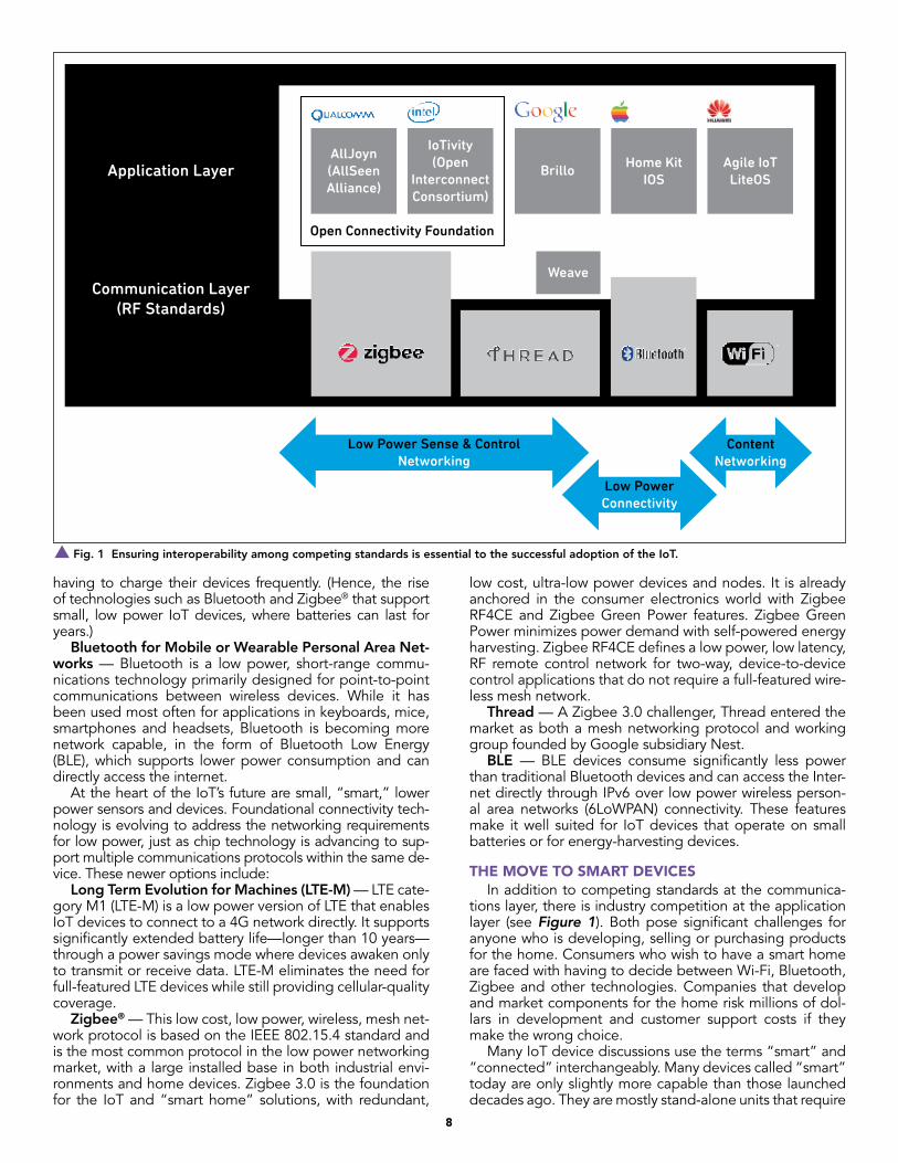
THE MOVE TO SMART DEVICESIn addition to competing standards at the communica-
tions layer, there is industry competition at the application layer (see Figure 1). Both pose significant challenges for anyone who is developing, selling or purchasing products for the home. Consumers who wish to have a smart home are faced with having to decide between Wi-Fi, Bluetooth, Zigbee and other technologies. Companies that develop and market components for the home risk millions of dol-lars in development and customer support costs if they make the wrong choice.
Many IoT device discussions use the terms “smart” and “connected” interchangeably. Many devices called “smart” today are only slightly more capable than those launched decades ago. They are mostly stand-alone units that require
having to charge their devices frequently. (Hence, the rise of technologies such as Bluetooth and Zigbee® that support small, low power IoT devices, where batteries can last for years.)
Bluetooth for Mobile or Wearable Personal Area Net-works — Bluetooth is a low power, short‐range commu-nications technology primarily designed for point‐to‐point communications between wireless devices. While it has been used most often for applications in keyboards, mice, smartphones and headsets, Bluetooth is becoming more network capable, in the form of Bluetooth Low Energy (BLE), which supports lower power consumption and can directly access the internet.
At the heart of the IoT’s future are small, “smart,” lower power sensors and devices. Foundational connectivity tech-nology is evolving to address the networking requirements for low power, just as chip technology is advancing to sup-port multiple communications protocols within the same de-vice. These newer options include:
Long Term Evolution for Machines (LTE-M) — LTE cate-gory M1 (LTE-M) is a low power version of LTE that enables IoT devices to connect to a 4G network directly. It supports significantly extended battery life—longer than 10 years—through a power savings mode where devices awaken only to transmit or receive data. LTE-M eliminates the need for full-featured LTE devices while still providing cellular-quality coverage.
Zigbee® — This low cost, low power, wireless, mesh net-work protocol is based on the IEEE 802.15.4 standard and is the most common protocol in the low power networking market, with a large installed base in both industrial envi-ronments and home devices. Zigbee 3.0 is the foundation for the IoT and “smart home” solutions, with redundant,
s Fig. 1 Ensuring interoperability among competing standards is essential to the successful adoption of the IoT.
Application LayerAllJoyn(AllSeenAlliance)
IoTivity(Open
InterconnectConsortium)
Brillo Home KitIOS
Agile IoTLiteOS
Open Connectivity Foundation
Communication Layer(RF Standards)
Weave
Low Power Sense & ControlNetworking
Low PowerConnectivity
ContentNetworking
9
and purchase equipment and try to guess which wireless technology standard to use, the consumer simply relies on the providers of the services they already use, such as inter-net access, security and entertainment. Their routers, mo-dems and set-top boxes are already in the home, and cus-tomers are accustomed to paying a monthly bill for these services. Consumers can select the services they want and control them through a single smartphone app.
Retail organizations that provide some home services, such as Wal-Mart, Home Depot, Costco and others, could easily enter this market. Large security firms and integrators could market an entire suite of services as a unified pack-age.
Applications and BenefitsThe benefits of the SHaaS are limited only by the imagi-
nation. Here are a few examples:Comfort, Cost Savings and Sustainability — If a family
were watching a movie on a cold winter night, a smart home system would turn off the lights and turn down the heat in the empty parts of the home. Power-consuming devices that are on but not in use would also be turned off. The sys-tem would lower the temperature for sleeping during the night and begin to raise it again before the family awakens and begins the day. If the home network recognizes that the family is away on vacation, it would disconnect devices that consume standby power.
Connecting the water heater to a smart sensor would allow leaks to be detected early. The smart sensor would alert the homeowner and also control the power and water systems connected to it. With smart sensors, homeowners can remotely run their dishwashers and appliances. Prob-lems would automatically be detected and relayed to a re-pair service. Home energy use and repair costs would be reduced and natural resources conserved. Insurance com-panies already are noting smart home applications that pro-vide early warning of water leaks, heating system defects and fire, which can reduce repair, renovation and replace-ment costs.
Senior Lifestyle — Many of us are living longer and want to remain independent. The SHaaS for seniors can help keep us safe and comfortable in our own homes without feeling that we are being watched by cameras. To do so, a limited number of small, battery-powered sensors for mo-tion detection and door opening and closing, strategically placed throughout the residence, would “observe” activi-ties and collect data. When something out of the ordinary occurs, the system would automatically notify family mem-bers, a friend or emergency personnel.
Fitness and Healthcare — Wearable lifestyle and fit-ness technology would integrate many more data points, including from sensors in the home, and help ensure proper nutrition and rest based on our health goals and medical histories.
INDUSTRIAL IoT The IoT is destined to have a profound impact, well be-
yond the home environment. It will transform virtually all industries, from hospitality and retail to automotive, agri-culture and healthcare, altering the way that municipalities and public services operate. For example, smart cities of the future will likely leverage the IoT for city lighting man-
human action to be turned on and off. For example, while a home security sensor may be “connected” and detects that no one is in the home, it does not interact with the lighting sensor to turn off the lights or with the heating system to turn down the thermostat.
A smart device and application can analyze incoming data and make a decision to control or activate a device without human intervention. In the case of the smart home environment, a network of devices can sense who is in the home, where they are in the home and learn what “nor-mal” activity is at a particular day and time. Using this intel-ligence about the residents, the network makes decisions about whether to lock doors and windows; turn on or off the heater, air conditioner, lights or entertainment system; or activate the security system. To be considered “smart,” a device must have three capabilities: • Connect to and exchange data with other smart or con-
nected devices in the home• Recognize what goes on in the home and learn what is
normal, beyond being programmed for a certain func-tion at a certain time
• Use a single integrated application on a smart phone or other web-connected device to manage all the functions.
THE SMART HOME AS A SERVICEWhile the IoT ultimately will affect every aspect of how
our world operates, the home environment provides an ex-cellent example of what is emerging as the future of the IoT as a service. Consumers are making it clear that they want more than a collection of sensors in their homes. They are not really seeking to own smart technology, rather they are looking for smart services and the ability of those services to help manage their lives.
The Smart Home as a Service (SHaaS) is the next phase of the home IoT evolution. SHaaS is a collection of services where devices, sensors and applications work together without human interaction. This network makes intelligent decisions that render homes more comfortable, safe and energy efficient. SHaaS solutions can reduce the number of sensors required in the home, and a single sensor can be used for a variety of applications. For example, a motion sensor can be used for the security system, light control, managing the temperature and controlling entertainment and senior lifestyle systems. There are four components of a SHaaS:• A network of sensors in the home provides a general in-
dication of when and where movement occurs, the envi-ronmental conditions and whether the home is secure or there are issues, such as a leak
• The information derived from these sensors is wirelessly collected by a local hub (e.g., gateway or set-top box) and securely transmitted to an intelligent cloud service that collects and analyzes the data and sends alerts to family members when it detects changes
• A central management app enables the consumer to manage the network using a single user interface on a smartphone or any web-connected device
• The service provider is easily able to handle customer support, billing, subscriber management, software and service upgrades and changes.
A SHaaS eliminates the need for the consumer to be technology-savvy. Rather than having to research, select

10
Cees Links is a pioneer of the wireless data industry and the man who led the team that created and popularized Wi-Fi. Cees was the founder and CEO of GreenPeak Technologies, a Smart Home and IoT radio communications semiconductor company, now part of Qorvo. After Qorvo’s acquisition of GreenPeak in 2016, Cees has become the Gen-eral Manager of the Wireless Connectivity business unit in Qorvo. He was recognized as Wi-Fi pioneer with the Golden Mousetrap Lifetime Achievement award.
agement, traffic flow monitoring and control, emergency services deployment and natural resource management.
In manufacturing, the increasing complexity of just-in-time supply chain processes will benefit from IoT appli-cations that enable more precise forecasting, inventory tracking and delivery of needed parts, as well as better col-laboration between suppliers and customers. Biosensors in the healthcare environment will speed testing and accurate diagnosis of a wide variety of conditions. They will also monitor the ecosystems related to wellness, such as water quality, drug and food safety.
IT’S ALL ABOUT SERVICESWhile advancing technology is essential to the future of
the IoT, the goal of a more connected world is really about services. These services will enable informed decisions faster than ever, allowing us to better manage our lives as individuals and families and operate more efficiently as or-ganizations.
A unified, smart IoT network, such as a SHaaS, delivers the benefits of connectivity, without the need for users to be technical experts. Device and system technologists can help realize the full potential of the IoT as a service by work-ing together to develop the hardware, software and web intelligence that will make this possible.n
JFW’s a world-leader in RF Attenuators and Switches.
Our components and our RF test systems & matrix switches are
designed for OEM and laboratory applications in 5G, IOT,
Satcom, Public-Safety, and Defense. Visit www.jfwindustries.com
to see the thousands of off-the-shelf models or to learn more
about our custom capabilities (with no NRE!).
jfwindustries.com
Simulation Speeds NB-IoT Product DevelopmentTakao Inoue and David VyeAWR Group, NI, El Segundo, Calif.
A nalysts from technology research firm Gartner are predicting a population of over 26 billion devices—excluding smartphones, tablets and comput-
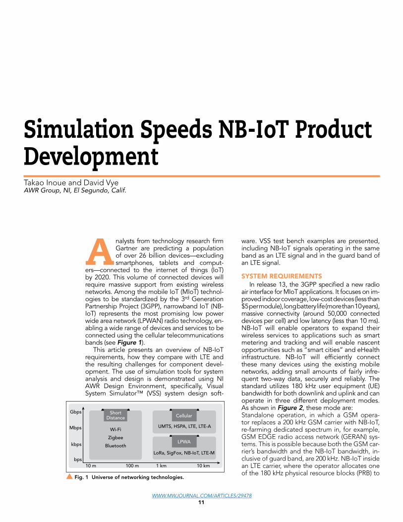
ers—connected to the internet of things (IoT) by 2020. This volume of connected devices will require massive support from existing wireless networks. Among the mobile IoT (MIoT) technol-ogies to be standardized by the 3rd Generation Partnership Project (3GPP), narrowband IoT (NB-IoT) represents the most promising low power wide area network (LPWAN) radio technology, en-abling a wide range of devices and services to be connected using the cellular telecommunications bands (see Figure 1).
This article presents an overview of NB-IoT requirements, how they compare with LTE and the resulting challenges for component devel-opment. The use of simulation tools for system analysis and design is demonstrated using NI AWR Design Environment, specifically, Visual System Simulator™ (VSS) system design soft-
ware. VSS test bench examples are presented, including NB-IoT signals operating in the same band as an LTE signal and in the guard band of an LTE signal.
SYSTEM REQUIREMENTSIn release 13, the 3GPP specified a new radio
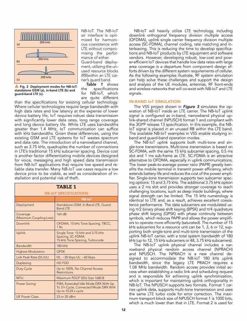
air interface for MIoT applications. It focuses on im-proved indoor coverage, low-cost devices (less than $5 per module), long battery life (more than 10 years), massive connectivity (around 50,000 connected devices per cell) and low latency (less than 10 ms). NB-IoT will enable operators to expand their wireless services to applications such as smart metering and tracking and will enable nascent opportunities such as “smart cities” and eHealth infrastructure. NB-IoT will efficiently connect these many devices using the existing mobile networks, adding small amounts of fairly infre-quent two-way data, securely and reliably. The standard utilizes 180 kHz user equipment (UE) bandwidth for both downlink and uplink and can operate in three different deployment modes. As shown in Figure 2, these mode are:Standalone operation, in which a GSM opera-tor replaces a 200 kHz GSM carrier with NB-IoT, re-farming dedicated spectrum in, for example, GSM EDGE radio access network (GERAN) sys-tems. This is possible because both the GSM car-rier’s bandwidth and the NB-IoT bandwidth, in-clusive of guard band, are 200 kHz. NB-IoT inside an LTE carrier, where the operator allocates one of the 180 kHz physical resource blocks (PRB) to
WWW.MWJOURNAL.COM/ARTICLES/2947811
s Fig. 1 Universe of networking technologies.
Gbps
Mbps
kbps
bps10 m 100 m 1 km 10 km
ShortDistance
Wi-Fi
Zigbee
Bluetooth
UMTS, HSPA, LTE, LTE-A
LoRa, SigFox, NB-IoT, LTE-M
Cellular
LPWA
12
NB-IoT will heavily utilize LTE technology, including downlink orthogonal frequency division multiple access (OFDMA), uplink single carrier frequency division multiple access (SC-FDMA), channel coding, rate matching and in-terleaving. This is reducing the time to develop specifica-tions and NB-IoT products by LTE equipment and software vendors. However, developing robust, low-cost and pow-er-efficient IoT devices that handle low data rates with large area coverage is a departure from component design ef-forts driven by the different system requirements of cellular. As the following examples illustrate, RF system simulation can help solve these challenges and support the design and analysis of the UE modules, antennas, RF front-ends and wireless networks that will co-exist with NB-IoT and LTE signals.
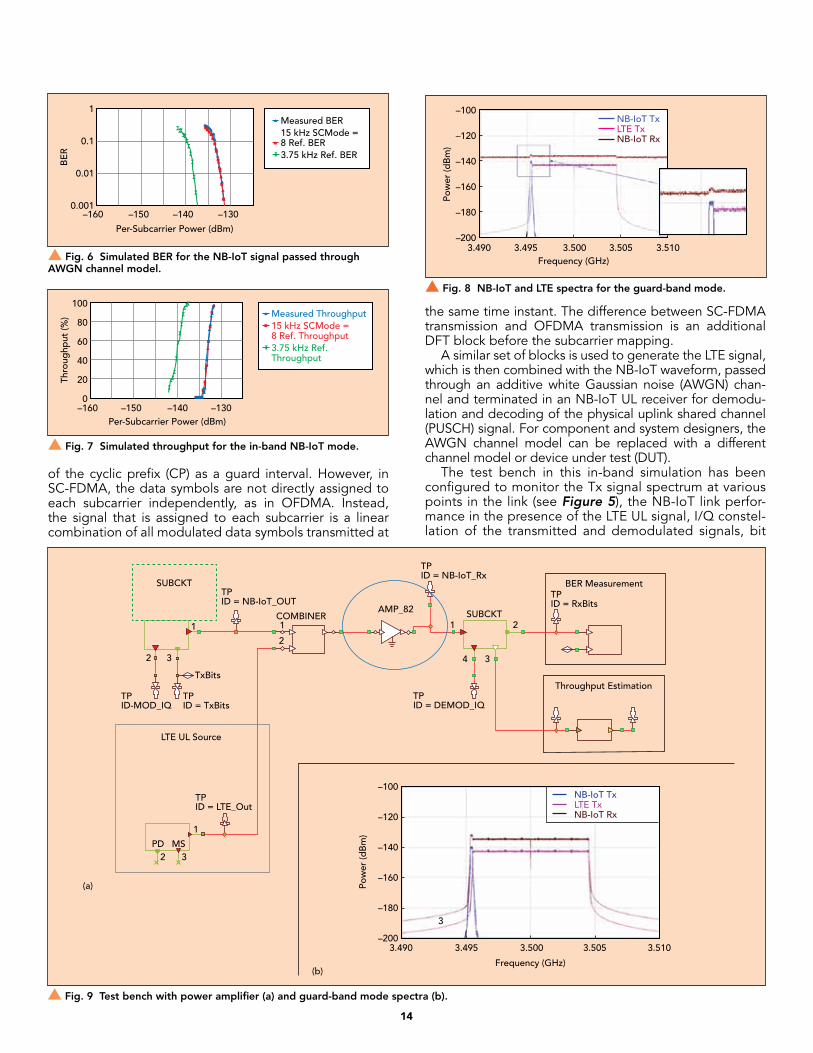
IN-BAND IoT SIMULATIONThe VSS project shown in Figure 3 simulates the op-
eration of NB-IoT inside an LTE carrier. The NB-IoT uplink signal is configured as in-band, narrowband physical up-link-shared channel (NPUSCH) format 1 and compliant with the 3GPP release 13 specification. In this example, the NB-IoT signal is placed in an unused RB within the LTE band. The available NB-IoT examples in VSS enable studying in-band and guard-band operation modes.
The NB-IoT uplink supports both multi-tone and sin-gle-tone transmissions. Multi-tone transmission is based on SC-FDMA, with the same 15 kHz subcarrier spacing, 0.5 ms slot and 1 ms sub-frame as LTE. SC-FDMA is an attractive alternative to OFDMA, especially in uplink communications. The lower peak-to-average power ratio (PAPR) greatly ben-efits the mobile terminal in transmit power efficiency, which extends battery life and reduces the cost of the power ampli-fier. Single-tone transmission supports two subcarrier spac-ing options: 15 and 3.75 kHz. The additional 3.75 kHz option uses a 2 ms slot and provides stronger coverage to reach challenging locations, such as deep inside buildings, where signal strength can be limited. The 15 kHz numerology is identical to LTE and, as a result, achieves excellent coexis-tence performance. The data subcarriers are modulated us-ing π/2 binary phase shift keying (BPSK) and π/4 quadrature phase shift keying (QPSK) with phase continuity between symbols, which reduces PAPR and allows the power amplifi-ers to operate more efficiently (saturated). The number of 15 kHz subcarriers for a resource unit can be 1, 3, 6 or 12, sup-porting both single-tone and multi-tone transmission of the uplink NB-IoT carrier, with a total system bandwidth of 180 kHz (up to 12, 15 kHz subcarriers or 48, 3.75 kHz subcarriers).
The NB-IoT uplink physical channel includes a nar-rowband physical random access channel (NPRACH) and NPUSCH. The NPRACH is a new channel de-signed to accommodate the NB-IoT 180 kHz uplink bandwidth, since the legacy LTE PRACH requires a 1.08 MHz bandwidth. Random access provides initial ac-cess when establishing a radio link and scheduling request and is responsible for achieving uplink synchronization, which is important for maintaining uplink orthogonality in NB-IoT. The NPUSCH supports two formats. Format 1 car-ries uplink data, supports multi-tone transmission and uses the same LTE turbo code for error correction. The maxi-mum transport block size of NPUSCH format 1 is 1000 bits, which is much lower than that in LTE. Format 2 is used for
NB-IoT. The NB-IoT air interface is opti-mized for harmoni-ous coexistence with LTE without compro-mising the perfor-mance of either.Guard-band deploy-ment, utilizing the un-used resource blocks (RB)within an LTE car-rier’s guard band.
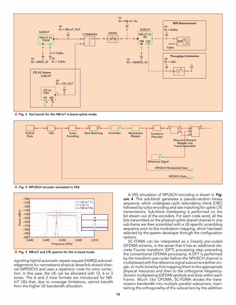
Table 1 shows the specifications for NB-IoT, which are quite different
than the specifications for existing cellular technology. Where cellular technologies require large bandwidth with high data rates and low latency at the expense of lower device battery life, IoT requires robust data transmission with significantly lower data rates, long range coverage and long device battery life. While LTE uses bandwidths greater than 1.4 MHz, IoT communication can suffice with kHz bandwidths. Given these differences, using the existing GSM and LTE systems for IoT wastes spectrum and data rate. The introduction of a narrowband channel, such as 3.75 kHz, quadruples the number of connections in LTE’s traditional 15 kHz subcarrier spacing. Device cost is another factor differentiating mobile devices designed for voice, messaging and high speed data transmission from NB-IoT applications that require low speed and re-liable data transfer. Many NB-IoT use cases require a low device price to be viable, as well as consideration of in-stallation and potential risk of theft.
s Fig. 2 Deployment modes for NB-IoT: standalone GSM (a), in-band LTE (b) and guard-band LTE (c).
200 kHz
200 kHz
200 kHz
(a)
(b)
(c)
TABLE 1NB-IoT SPECIFICATIONS
NB-IoT
Deployment Standalone GSM, In-Band LTE, Guard-Band LTE
Coverage (Maximum Coupling Loss)
164 dB
Downlink OFDMA, 15 kHz Tone Spacing, TBCC, 1 Rx
Uplink Single Tone: 15 kHz and 3.75 kHz Spacing, SC-FDMA: 15 kHz Tone Spacing, Turbocode
Bandwidth 180 kHz
Highest Modulation QPSK
Link Peak Rate (DL/UL) DL: ~30 kbps UL: ~60 kbps
Duplexing HD FDD
Duty Cycle Up to 100%, No Channel Access Restrictions
MTU Maximum PDCP SDU Size 1600 B
Power Saving PSM, Extended Idle Mode DRX With Up To 3 h Cycle, Connected Mode DRX With Up to 10.24 s cycle
UE Power Class 23 or 20 dBm
13
A VSS simulation of NPUSCH encoding is shown in Fig-ure 4. This sub-block generates a pseudo-random binary sequence, which undergoes cyclic redundancy check (CRC) followed by turbo encoding and rate matching for uplink LTE transmissions. Sub-block interleaving is performed on the bit stream out of the encoders. For each code word, all the bits transmitted on the physical uplink shared channel in one sub-frame are then scrambled with a UE-specific scrambling sequence prior to the modulation mapping, which has been selected by the system developer through the configuration options.
SC-FDMA can be interpreted as a linearly pre-coded OFDMA scheme, in the sense that it has an additional dis-crete Fourier transform (DFT) processing step preceding the conventional OFDMA processing. A DFT is performed by the transform pre-coder before the NPUSCH channel is multiplexed with the reference signal subcarriers (either sin-gle- or multi-tone) by first mapping them to the appropriate physical resources and then to the orthogonal frequency- division multiplexing (OFDM) symbols and slots within each frame. Much like OFDMA, SC-FDMA divides the trans-mission bandwidth into multiple parallel subcarriers, main-taining the orthogonality of the subcarriers by the addition
signaling hybrid automatic repeat request (HARQ) acknowl-edgements for narrowband physical downlink shared chan-nel (NPDSCH) and uses a repetition code for error correc-tion. In this case, the UE can be allocated with 12, 6 or 3 tones. The 6 and 3 tone formats are introduced for NB-IoT UEs that, due to coverage limitations, cannot benefit from the higher UE bandwidth allocation.
s Fig. 3 Test bench for the NB-IoT in-band uplink mode.
BER Measurement
Throughput Estimation
SUBCKT
SUBCKT
SUBCKTCOMBINER
LTE UL Source
TPID = NB-IoT_Rx
TPID = TxBits
TPID = RxBits
TPID = LTE_OUT
TPID = NB-IoT_OUT
LTE ULTSIG
PD MS
CRCMB
1
2 3
TPID = MOD_IQ
TPID = DEMOD_IQ
TPID = GRC
AWGN
TxBits
NB-IoT ULTSIGE
NB-IoT ULRX
TxBits
BER
s Fig. 4 NPUSCH encoder simulated in VSS.
PUSCHData
TurboEncoding
1 2 1 2 1
1
1 42233Rate Matching Modulation
MapperTransformPrecoder
Resource ElementMapper and
Frame Assembler
NPUSCH Modulated Data
NPUSCH Data
Reference Signal
ScramblerCRC
s Fig. 5 NB-IoT and LTE spectra for the in-band mode.
–100–110–120–130–140–150–160–170–180–190–200
3.5103.5053.5003.4953.490Frequency (GHz)
Pow
er (d
Bm
)
NB-IoT TxLTE TxNB-IoT Rx
14
the same time instant. The difference between SC-FDMA transmission and OFDMA transmission is an additional DFT block before the subcarrier mapping.
A similar set of blocks is used to generate the LTE signal, which is then combined with the NB-IoT waveform, passed through an additive white Gaussian noise (AWGN) chan-nel and terminated in an NB-IoT UL receiver for demodu-lation and decoding of the physical uplink shared channel (PUSCH) signal. For component and system designers, the AWGN channel model can be replaced with a different channel model or device under test (DUT).
The test bench in this in-band simulation has been configured to monitor the Tx signal spectrum at various points in the link (see Figure 5), the NB-IoT link perfor-mance in the presence of the LTE UL signal, I/Q constel-lation of the transmitted and demodulated signals, bit
of the cyclic prefix (CP) as a guard interval. However, in SC-FDMA, the data symbols are not directly assigned to each subcarrier independently, as in OFDMA. Instead, the signal that is assigned to each subcarrier is a linear combination of all modulated data symbols transmitted at
s Fig. 7 Simulated throughput for the in-band NB-IoT mode.
100
80
60
40
20
0–130–140–150–160
Per-Subcarrier Power (dBm)
Measured Throughput15 kHz SCMode = 8 Ref. Throughput3.75 kHz Ref. Throughput
Thro
ughp
ut (%
)
s Fig. 6 Simulated BER for the NB-IoT signal passed through AWGN channel model.
1
0.1
0.01
0.001–140–150–160 –130
Measured BER15 kHz SCMode = 8 Ref. BER3.75 kHz Ref. BER
Per-Subcarrier Power (dBm)
BE
R
s Fig. 8 NB-IoT and LTE spectra for the guard-band mode.
–100
–120
–140
–160
–180
–2003.5103.5053.5003.4953.490
Pow
er (d
Bm
)
Frequency (GHz)
NB-IoT TxLTE TxNB-IoT Rx
s Fig. 9 Test bench with power amplifier (a) and guard-band mode spectra (b).
Frequency (GHz)
COMBINER
SUBCKT
SUBCKT
BER Measurement
Throughput Estimation
NB-IoT Tx LTE Tx NB-IoT Rx
LTE UL Source
TPID = LTE_Out
TPID = TxBits
TPID-MOD_IQ
TxBits
TPID = NB-IoT_OUT
1
1 1
2
–100
–120
–140
–160
–180
–2003.5103.5053.5003.4953.490
2 3
21
34
3
2 3
TPID = DEMOD_IQ
TPID = NB-IoT_Rx
TPID = RxBitsAMP_82
Pow
er (d
Bm
)
(a)
PD MS
(b)
15
error rate (BER) (see Figure 6), block error rate (BLER), throughput (see Figure 7) and the CRC error for each block.
GUARD-BAND NB-IoT SIMULATIONA related example demonstrates operation of NB-IoT in
the guard band of an LTE signal. The project is essentially the same as in the previous example with a simple change to the NB-IoT RB location. For guard-band operation, the NB-IoT RB is set to be greater than zero or greater than N_RB_UL, the upper limit, to operate in the lower or upper guard band, respectively. In-band operation is obtained by setting the NB-IoT RB at any value between these limits. The spectra for an NB-IoT channel operating in guard-band mode is shown in Figure 8.
As previously mentioned, a front-end module, pow-er amplifier and antenna design can be added to or sub-stituted for the AWGN channel model, which serves as a placeholder for a DUT. Figure 9 shows an amplifier inserted between the UL transmitter and receiver. The simulation al-lows designers to sweep various parameters, such as input power, or toggle different NB-IoT subcarrier modulation schemes (π/2 BPSK or π/4 QPSK) to investigate the impact on performance, such as error vector magnitude (EVM).
CONCLUSIONThe NB-IoT standard specified in 3GPP release 13 lever-
ages the existing LTE network to support a future ecosystem of low-cost IoT devices. While the use of the existing LTE in-frastructure with relaxed performance requirements, due to the lower data rates, will help offset some design challenges, the need for low cost, increased coverage area and longer battery life with sustained reachability introduces some dif-ficult-to-achieve requirements. VSS and other system simu-lation tools aid NB-IoT system development by simulating designs pre-silicon, saving valuable time and effort bringing these new products to market.n
Antenna Technologies for the FuturePatrick HindleMicrowave Journal Editor
Traditional antenna technology has hit its limits in many demanding commer-cial and aerospace markets such as 5G, SATCOM, IoT and radar. But there are
many companies developing new approaches and materials that could drastically improve an-tenna performance and enable new applications that were not previously envisioned because of these limitations. In this article, Microwave Jour-nal looks at a sampling of these technologies that have come to our attention in the last cou-ple of years.
3D PRINTED ANTENNASRecent advances in 3D printing or additive
manufacturing have enabled complex RF struc-tures to be realized. The characterization of the materials used in 3D printing processes has been shown to be critical in designing and accu-rately predicting the performance of these struc-tures. Understanding the RF properties of the materials through characterization has led to the development of novel structures that could not ever be realized with traditional manufacturing techniques. 3D printing has also allowed manu-facturers to produce traditional antenna shapes with less weight and at a lower cost.
SWISSto12 SA is an offshoot from the Swiss Federal Institute of Technology in Lausanne, Switzerland. The company has developed unique products using 3D printing that are
based on polymer materials that are then metal plated or on metallic materials (such as alumi-num or titanium) combined with advanced sur-face treatments and surface plating. Using these processes, SWISSto12 manufactures and tests aerospace qualified advanced RF products such as waveguides, filters, beamforming networks, antenna feed chains or array antennas.
Their use of 3D printing allows for increased flexibility in the manufacturing of complex prod-uct designs. This freedom can be used to pro-duce higher complexity RF components, which often allows for better RF performance. Tradi-tional machining technologies used to manu-facture RF products are limited in their ability to produce products with complex shapes. To circumvent this limitation, complex products are often assembled out of a larger number of sim-pler sub-components that are produced sepa-rately. SWISSto12’s 3D printing technology does not have such constraints, allowing it to pro-duce entire products in one single element that positively impact mass, cost, lead time, assem-bly quality and RF performance. The use of 3D printing also allows for optimized weight reduc-tion. The technology has been demonstrated on waveguide, filter and antenna components from C- to W-Band (4 to 110 GHz).
As this technology is rapidly gaining maturity and acceptance among the aerospace indus-try, SWISSto12 has already delivered a variety
WWW.MWJOURNAL.COM/ARTICLES/2957216
17
larizations. Addition-ally, the right- hand combiner network feeds into a dual-axis monopulse compar-ator. All of this is im-plemented in a sin-gle part that weighs less than 2 oz and fits in the palm of the hand.
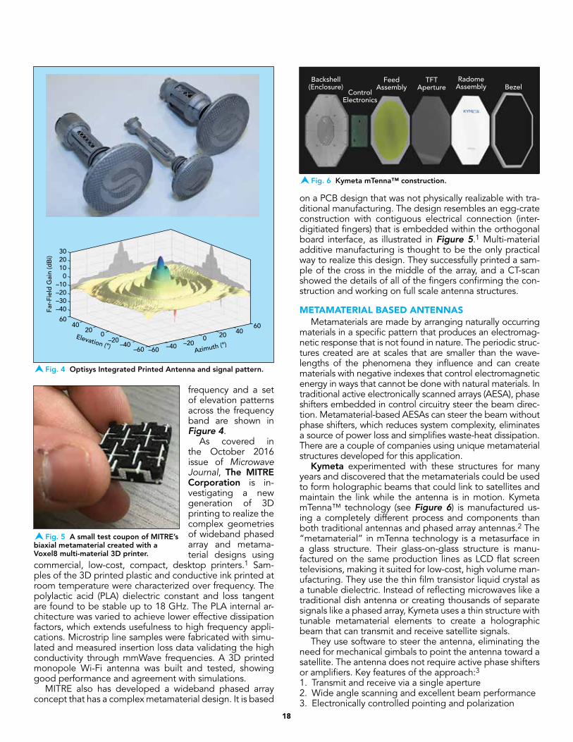
A second array design is the X64 an-tenna that takes the integration a step fur-ther, by including a waveguide dual-axis monopulse compara-tor on both polariza-tions and integrating an elevation rotation axis into the design. Fabricating this part in a traditional process would require well over 100 separate parts, compared to the single printed part. Signal patterns are shown for sum, delta elevation and delta azimuth on the right-hand circular polarization (see Figure 3). There are a total of eight simultaneous antenna beams gener-ated in this antenna.
Another key area of innovation where Optisys has gen-erated interest is in the design and building of lightweight feeds for parabolic reflectors, where the sub-reflector, feed horn and polarizer are printed as a single metal part with-out blockage or losses due to struts or a dielectric support. This design has been optimized to the key frequency bands of X-, Ku- and Ka-Band. The company refers to these an-tenna feeds as the integrated printed antenna family of feeds. The unit and 3D near-field scan pattern at a single
of prototypes to or-ganizations in the space and SATCOM industries that have been qualified for use in airborne and space environments (the first commer-cial programs will be flying SWISSto12 products in 2018). More complex and integrated antenna or payload structures are in development, in particular Ku- and Ka-Band products. The company is also targeting emerging market opportunities such as high-altitude platforms, UAVs and Cubesat constella-tions. An example antenna product is a Ku-Band dual-reflec-tor antenna compris-ing a conical chocked horn, a sub-reflector,
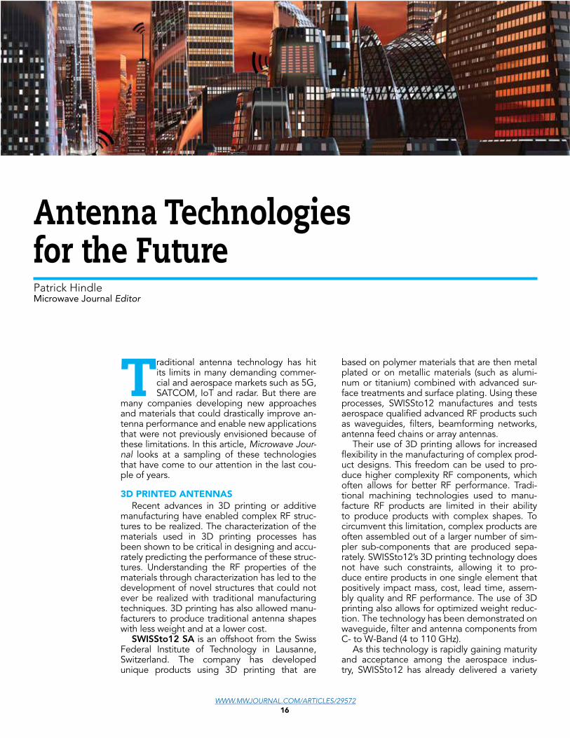
a main reflector and metallic supports. This antenna system only weighs 145 g. The radiation properties of this antenna were found to be in an excellent agreement with simulation results over the design frequency range (see Figure 1). This antenna demonstrator was manufactured and tested in col-laboration with the European Space Agency.
Optisys is another company that focuses on the design, fabrication and test of lightweight antennas using metal 3D printing. The specific method that Optisys uses for fabrica-tion is a powder bed fusion process, where thin layers of powder are welded into solid metal by a high-power laser. Through this welding process, a part is built one small lay-er at a time. This green manufacturing process allows for material to be added only where absolutely necessary to achieve a given mechanical or RF function.
As with any fabrication process, 3D printing has a set of design rules that determines what can and cannot be included in a design. Optisys is reimagining how waveguide is routed to achieve a desired RF function to take full advantage of the strengths of the printing process that allows, in some cases, for over an order-of-magnitude reduction in the size and weight of an antenna. Along with size and weight, part count reduc-tions and absorbing tolerance stack-up can lead to simpler antenna assemblies with improved performance.
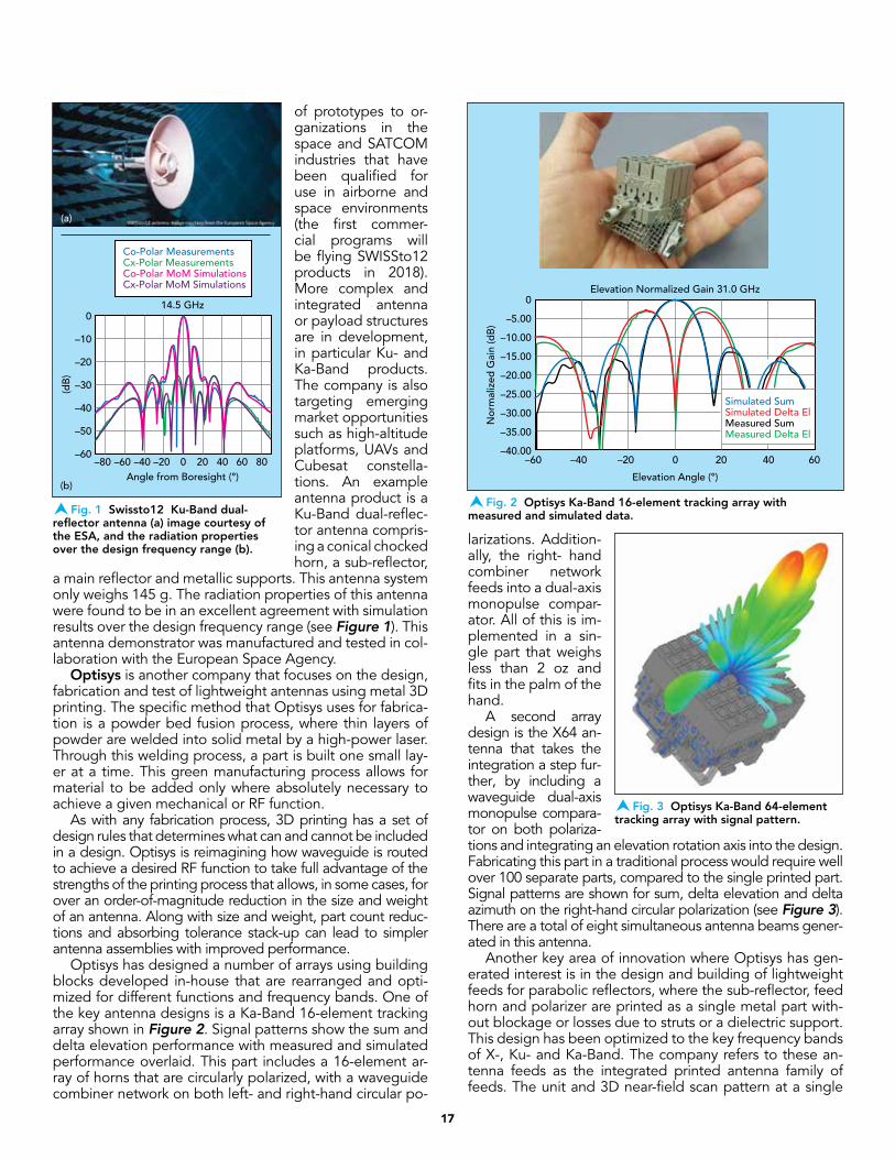
Optisys has designed a number of arrays using building blocks developed in-house that are rearranged and opti-mized for different functions and frequency bands. One of the key antenna designs is a Ka-Band 16-element tracking array shown in Figure 2. Signal patterns show the sum and delta elevation performance with measured and simulated performance overlaid. This part includes a 16-element ar-ray of horns that are circularly polarized, with a waveguide combiner network on both left- and right-hand circular po-
Fig. 1 Swissto12 Ku-Band dual-reflector antenna (a) image courtesy of the ESA, and the radiation properties over the design frequency range (b).
0
–10
–20
–30
–40
–50
–60806040200–20–40–60–80
(dB
)
Angle from Boresight (°)
14.5 GHz
(a)
(b)
Co-Polar MeasurementsCx-Polar MeasurementsCo-Polar MoM SimulationsCx-Polar MoM Simulations
Fig. 2 Optisys Ka-Band 16-element tracking array with measured and simulated data.
0
–5.00
–10.00
–15.00
–20.00
–25.00
–30.00
–35.00
–40.006040200–20–40–60
Nor
mal
ized
Gai
n (d
B)
Elevation Normalized Gain 31.0 GHz
Elevation Angle (°)
Simulated Sum Simulated Delta ElMeasured Sum Measured Delta El
Fig. 3 Optisys Ka-Band 64-element tracking array with signal pattern.
18
on a PCB design that was not physically realizable with tra-ditional manufacturing. The design resembles an egg-crate construction with contiguous electrical connection (inter-digitiated fingers) that is embedded within the orthogonal board interface, as illustrated in Figure 5.1 Multi-material additive manufacturing is thought to be the only practical way to realize this design. They successfully printed a sam-ple of the cross in the middle of the array, and a CT-scan showed the details of all of the fingers confirming the con-struction and working on full scale antenna structures.
METAMATERIAL BASED ANTENNASMetamaterials are made by arranging naturally occurring
materials in a specific pattern that produces an electromag-netic response that is not found in nature. The periodic struc-tures created are at scales that are smaller than the wave-lengths of the phenomena they influence and can create materials with negative indexes that control electromagnetic energy in ways that cannot be done with natural materials. In traditional active electronically scanned arrays (AESA), phase shifters embedded in control circuitry steer the beam direc-tion. Metamaterial-based AESAs can steer the beam without phase shifters, which reduces system complexity, eliminates a source of power loss and simplifies waste-heat dissipation. There are a couple of companies using unique metamaterial structures developed for this application.
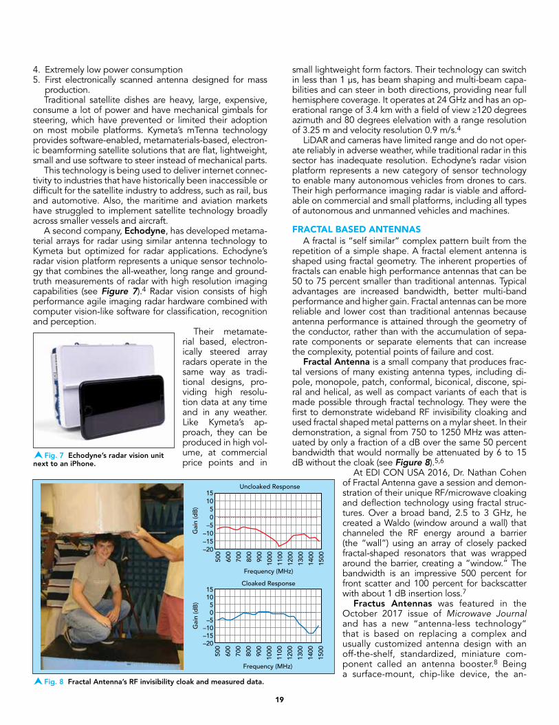
Kymeta experimented with these structures for many years and discovered that the metamaterials could be used to form holographic beams that could link to satellites and maintain the link while the antenna is in motion. Kymeta mTenna™ technology (see Figure 6) is manufactured us-ing a completely different process and components than both traditional antennas and phased array antennas.2 The “metamaterial” in mTenna technology is a metasurface in a glass structure. Their glass-on-glass structure is manu-factured on the same production lines as LCD flat screen televisions, making it suited for low-cost, high volume man-ufacturing. They use the thin film transistor liquid crystal as a tunable dielectric. Instead of reflecting microwaves like a traditional dish antenna or creating thousands of separate signals like a phased array, Kymeta uses a thin structure with tunable metamaterial elements to create a holographic beam that can transmit and receive satellite signals.
They use software to steer the antenna, eliminating the need for mechanical gimbals to point the antenna toward a satellite. The antenna does not require active phase shifters or amplifiers. Key features of the approach:31. Transmit and receive via a single aperture2. Wide angle scanning and excellent beam performance3. Electronically controlled pointing and polarization
frequency and a set of elevation patterns across the frequency band are shown in Figure 4.
As covered in the October 2016 issue of Microwave Journal, The MITRE Corporation is in-vestigating a new generation of 3D printing to realize the complex geometries of wideband phased array and metama-terial designs using
commercial, low-cost, compact, desktop printers.1 Sam-ples of the 3D printed plastic and conductive ink printed at room temperature were characterized over frequency. The polylactic acid (PLA) dielectric constant and loss tangent are found to be stable up to 18 GHz. The PLA internal ar-chitecture was varied to achieve lower effective dissipation factors, which extends usefulness to high frequency appli-cations. Microstrip line samples were fabricated with simu-lated and measured insertion loss data validating the high conductivity through mmWave frequencies. A 3D printed monopole Wi-Fi antenna was built and tested, showing good performance and agreement with simulations.
MITRE also has developed a wideband phased array concept that has a complex metamaterial design. It is based
Fig. 4 Optisys Integrated Printed Antenna and signal pattern.
3020100
–10–20–30–40
6060
4040
2020
00
–20–20–40–40
–60–60
Elevation (°)Azimuth (°)
Far-
Fiel
d G
ain
(dB
i)
Fig. 5 A small test coupon of MITRE’s biaxial metamaterial created with a Voxel8 multi-material 3D printer.
Fig. 6 Kymeta mTenna™ construction.
Backshell(Enclosure)
ControlElectronics
FeedAssembly
TFTAperture
RadomeAssembly Bezel
19
small lightweight form factors. Their technology can switch in less than 1 μs, has beam shaping and multi-beam capa-bilities and can steer in both directions, providing near full hemisphere coverage. It operates at 24 GHz and has an op-erational range of 3.4 km with a field of view ≥120 degrees azimuth and 80 degrees elelvation with a range resolution of 3.25 m and velocity resolution 0.9 m/s.4
LiDAR and cameras have limited range and do not oper-ate reliably in adverse weather, while traditional radar in this sector has inadequate resolution. Echodyne’s radar vision platform represents a new category of sensor technology to enable many autonomous vehicles from drones to cars. Their high performance imaging radar is viable and afford-able on commercial and small platforms, including all types of autonomous and unmanned vehicles and machines.
FRACTAL BASED ANTENNASA fractal is “self similar” complex pattern built from the
repetition of a simple shape. A fractal element antenna is shaped using fractal geometry. The inherent properties of fractals can enable high performance antennas that can be 50 to 75 percent smaller than traditional antennas. Typical advantages are increased bandwidth, better multi-band performance and higher gain. Fractal antennas can be more reliable and lower cost than traditional antennas because antenna performance is attained through the geometry of the conductor, rather than with the accumulation of sepa-rate components or separate elements that can increase the complexity, potential points of failure and cost.
Fractal Antenna is a small company that produces frac-tal versions of many existing antenna types, including di-pole, monopole, patch, conformal, biconical, discone, spi-ral and helical, as well as compact variants of each that is made possible through fractal technology. They were the first to demonstrate wideband RF invisibility cloaking and used fractal shaped metal patterns on a mylar sheet. In their demonstration, a signal from 750 to 1250 MHz was atten-uated by only a fraction of a dB over the same 50 percent bandwidth that would normally be attenuated by 6 to 15 dB without the cloak (see Figure 8).5,6
At EDI CON USA 2016, Dr. Nathan Cohen of Fractal Antenna gave a session and demon-stration of their unique RF/microwave cloaking and deflection technology using fractal struc-tures. Over a broad band, 2.5 to 3 GHz, he created a Waldo (window around a wall) that channeled the RF energy around a barrier (the “wall”) using an array of closely packed fractal-shaped resonators that was wrapped around the barrier, creating a “window.” The bandwidth is an impressive 500 percent for front scatter and 100 percent for backscatter with about 1 dB insertion loss.7
Fractus Antennas was featured in the October 2017 issue of Microwave Journal and has a new “antenna-less technology” that is based on replacing a complex and usually customized antenna design with an off-the-shelf, standardized, miniature com-ponent called an antenna booster.8 Being a surface-mount, chip-like device, the an-
4. Extremely low power consumption5. First electronically scanned antenna designed for mass
production.Traditional satellite dishes are heavy, large, expensive,
consume a lot of power and have mechanical gimbals for steering, which have prevented or limited their adoption on most mobile platforms. Kymeta’s mTenna technology provides software-enabled, metamaterials-based, electron-ic beamforming satellite solutions that are flat, lightweight, small and use software to steer instead of mechanical parts.
This technology is being used to deliver internet connec-tivity to industries that have historically been inaccessible or difficult for the satellite industry to address, such as rail, bus and automotive. Also, the maritime and aviation markets have struggled to implement satellite technology broadly across smaller vessels and aircraft.
A second company, Echodyne, has developed metama-terial arrays for radar using similar antenna technology to Kymeta but optimized for radar applications. Echodyne’s radar vision platform represents a unique sensor technolo-gy that combines the all-weather, long range and ground-truth measurements of radar with high resolution imaging capabilities (see Figure 7).4 Radar vision consists of high performance agile imaging radar hardware combined with computer vision-like software for classification, recognition and perception.
Their metamate-rial based, electron-ically steered array radars operate in the same way as tradi-tional designs, pro-viding high resolu-tion data at any time and in any weather. Like Kymeta’s ap-proach, they can be produced in high vol-ume, at commercial price points and in
Fig. 7 Echodyne’s radar vision unit next to an iPhone.
Fig. 8 Fractal Antenna’s RF invisibility cloak and measured data.
151050
–5–10–15–20
151050
–5–10–15–20
500
600
700
800
900
1000
1100
1200
1300
1400
1500
Uncloaked Response
Gai
n (d
B)
Gai
n (d
B)
Cloaked Response
Frequency (MHz)
500
600
700
800
900
1000
1100
1200
1300
1400
1500
Frequency (MHz)
20
low loss device. Due to their silicon IC construction, PSiDs can be reproduced with high precision for the mass market at low cost. They have high power handling and, unlike RF MEMS, can be “hot” switched.
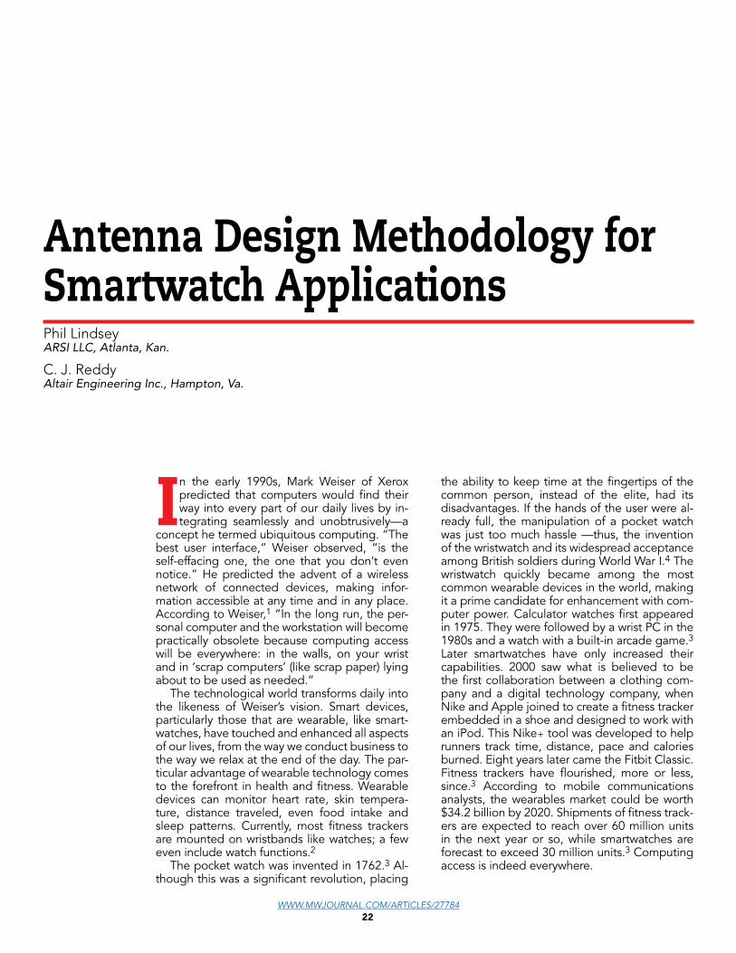
PSiAn uses either single or multiple PSiDs to perform azimuth and elevation beam steering. The PSiDs are mounted on RF PCBs and use transmission lines to link the device ports to traditional RF and antenna technolo-gies, such as LNAs, PAs, printed feeds, lenses and reflec-tors to produce efficient smart antennas with steerable narrow beams. Potential applications of PSiAn plasma antennas include: small cell backhaul at V-Band (60 GHz), gigabit wireless LAN (e.g. WiGig), intelligent transport systems (ITS) at 63 GHz and vehicle radar (77 GHz).
The company recently introduced an antenna that re-duces the cost of a 5G base station by up to 50 percent by eliminating phase shifters, reducing and consolidating amplification and reducing computation. The technology does not need calibration and can handle high-power, hav-ing been tested up to 40 W. The company has shown the technology in a variety of scenarios, including a 360 degree field of view, beamforming and steering, 28 GHz, 5 W, 16 dBi gain PSiAN, useful for pole mounted small cells, indoor small cells—also on a vehicle and a high-power, long range, low loss small cell base station antenna for standalone and MIMO 5G, fixed wireless access (FWA) and connected ve-hicle applications (see Figure 11).9 These devices can also be stacked to form and steer beams in two dimensions (az-imuth and elevation) or to form multiple beams and MIMO applications.
They also announced their mmWave PSiAn for use in smartphones and other consumer electronics, delivering high throughput with low latency and utilizing directional beams that generate less interference and maximize ener-gy efficiency.10 The introduction of mmWave connectivity for smartphones and other mobile devices faces significant problems as the signals are easily blocked by fingers, hands, heads and bodies. When used in combination with distrib-uted radiating elements, PSiDs can be used as a switch and beam former to utilize only elements that are able to re-ceive and transmit line-of-sight or reflected signals resolv-ing this issue. Plasma Antennas recently modeled plasma silicon corner antennas as replacements for array modules for device manufacturers and silicon suppliers. This ap-proach closely represented the publicly available solutions from Qualcomm and Samsung, for which there are many handling scenarios that would block the antennas. The ar-ray Plasma Antennas proposes now solves these problems and brings the intrinsic qualities of plasma silicon.
Gapwaves AB was founded in 2011 by Professor Per-Si-mon Kildal at Chalmers University of Technology in Gothen-burg, Sweden, with the aim of enabling efficient wireless com-munication through the patented GAP waveguide technolo-gy. GAP waveguides provide a unique packaging technology for mmWave and terahertz circuits and components, with ad-vantages compared to existing transmission line and wave-guide technology. The technology is based on an artificial magnetic conductor that enables contactless propagation of electromagnetic waves, significantly reducing transmission losses. The GAP waveguide is built up of two parts: a structured metal surface and a flat metal surface placed close to one another, allowing for an air gap between the two parts
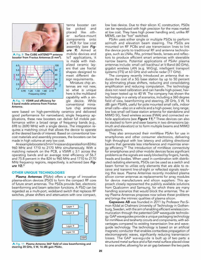
tenna booster can be picked and placed like oth-er surface-mount components onto a PCB for low cost assembly (see Fig-ure 9). Aimed at mobile devices and IoT applications, it is made with met-alized ceramic lay-ers that use fractal shapes designed to meet different de-sign requirements.
Miniature chip an-tennas are not new, so what is unique here is the multiband capability with a sin-gle device. While conventional minia-ture chip antennas
were based on high-permittivity ceramics and delivered good performance for narrowband, single frequency ap-plications, these new boosters can deliver full mobile per-formance within a broad range of frequency bands (e.g., 698 to 2690 MHz) with a single device. The integration re-quires a matching circuit that allows the device to operate at the desired bands of interest. Based on conventional low-cost materials and assembly processes, the boosters can be made in high volume at very low cost.
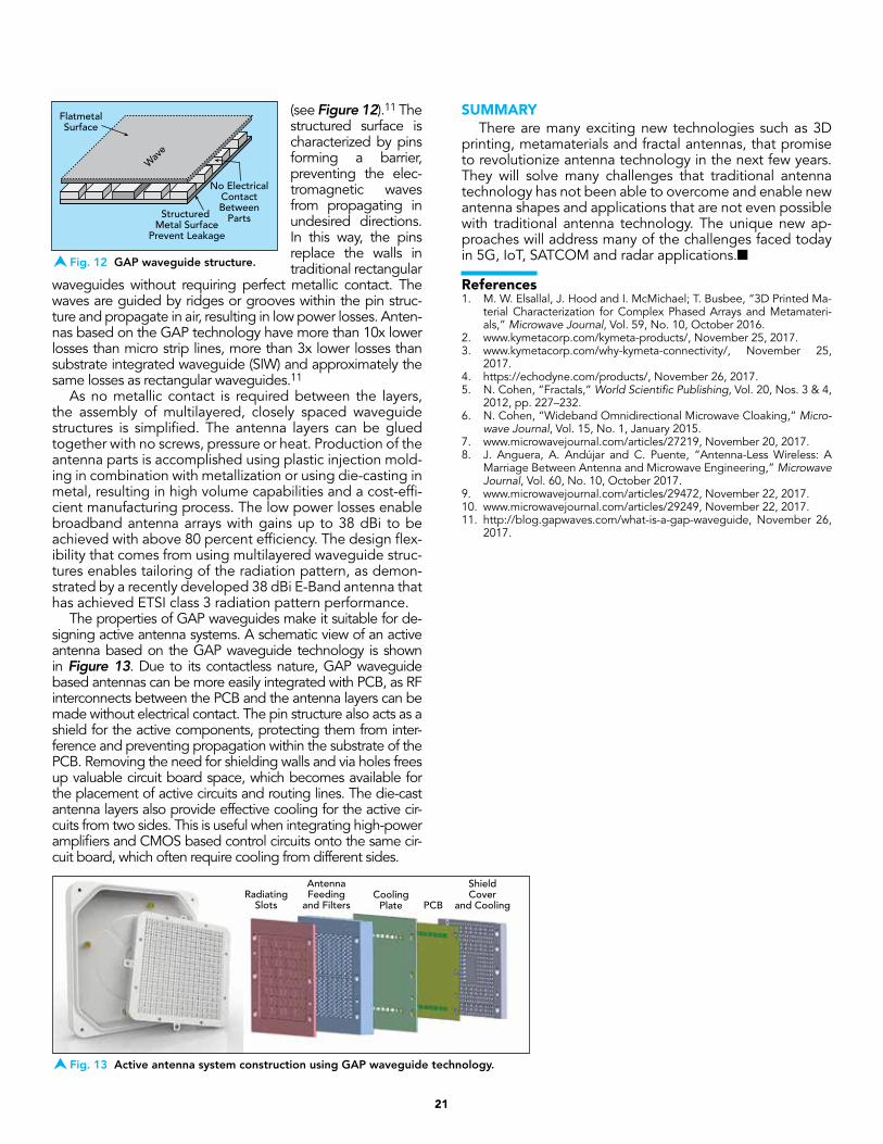
An example booster is 5 mm3 in size and operates from 824 to 960 MHz and 1710 to 2170 MHz simultaneously. With a matching network on the PCB, a VSWR ≤ 3:1 across the operating bands and an average total efficiency of 56.7 and 75.8 percent in the 824 to 960 MHz and 1710 to 2170 MHz frequency regions, respectively, is achieved (see Fig-ure 10).8
OTHER UNIQUE TECHNOLOGIESPlasma Antennas (PSiAn) offers a range of innovative
plasma-silicon devices (PSiD) to form the compact RF core of future smart antennas. The PSiDs provide fast, electronic beamforming and beam selection functions. A PSiD can be regarded as a multi-port, wideband switch that replaces RF switches, phase shifters and attenuators with one compact,
Fig. 9 The CUBE mXTEND™ antenna booster from Fractus Antennas (5 mm3).
Fig. 10 VSWR and efficiency for 5 band mobile antenna from Fractus Antenna.
6.0
5.0
4.0
3.0
2.0
1.02.101.801.501.200.90
100
80
60
40
20
0
Total Ef�ciency (%
)
VSW
R
Frequency (GHz)
VSWREf�ciency
Fig. 11 Plasma Antenna 360° field of view beamforming and steering 28 GHz, 5 W, 16 dBi gain PSiAn.
Layer 1
Layer 2
Layer 9
Layer 10
Dig
ital
DSP
21
SUMMARYThere are many exciting new technologies such as 3D
printing, metamaterials and fractal antennas, that promise to revolutionize antenna technology in the next few years. They will solve many challenges that traditional antenna technology has not been able to overcome and enable new antenna shapes and applications that are not even possible with traditional antenna technology. The unique new ap-proaches will address many of the challenges faced today in 5G, IoT, SATCOM and radar applications.n
References1. M. W. Elsallal, J. Hood and I. McMichael; T. Busbee, “3D Printed Ma-
terial Characterization for Complex Phased Arrays and Metamateri-als,” Microwave Journal, Vol. 59, No. 10, October 2016.
2. www.kymetacorp.com/kymeta-products/, November 25, 2017.3. www.kymetacorp.com/why-kymeta-connectivity/, November 25,
2017.4. https://echodyne.com/products/, November 26, 2017.5. N. Cohen, “Fractals,” World Scientific Publishing, Vol. 20, Nos. 3 & 4,
2012, pp. 227–232.6. N. Cohen, “Wideband Omnidirectional Microwave Cloaking,” Micro-
wave Journal, Vol. 15, No. 1, January 2015.7. www.microwavejournal.com/articles/27219, November 20, 2017.8. J. Anguera, A. Andújar and C. Puente, “Antenna-Less Wireless: A
Marriage Between Antenna and Microwave Engineering,” Microwave Journal, Vol. 60, No. 10, October 2017.
9. www.microwavejournal.com/articles/29472, November 22, 2017.10. www.microwavejournal.com/articles/29249, November 22, 2017.11. http://blog.gapwaves.com/what-is-a-gap-waveguide, November 26,
2017.
(see Figure 12).11 The structured surface is characterized by pins forming a barrier, preventing the elec-tromagnetic waves from propagating in undesired directions. In this way, the pins replace the walls in traditional rectangular
waveguides without requiring perfect metallic contact. The waves are guided by ridges or grooves within the pin struc-ture and propagate in air, resulting in low power losses. Anten-nas based on the GAP technology have more than 10x lower losses than micro strip lines, more than 3x lower losses than substrate integrated waveguide (SIW) and approximately the same losses as rectangular waveguides.11
As no metallic contact is required between the layers, the assembly of multilayered, closely spaced waveguide structures is simplified. The antenna layers can be glued together with no screws, pressure or heat. Production of the antenna parts is accomplished using plastic injection mold-ing in combination with metallization or using die-casting in metal, resulting in high volume capabilities and a cost-effi-cient manufacturing process. The low power losses enable broadband antenna arrays with gains up to 38 dBi to be achieved with above 80 percent efficiency. The design flex-ibility that comes from using multilayered waveguide struc-tures enables tailoring of the radiation pattern, as demon-strated by a recently developed 38 dBi E-Band antenna that has achieved ETSI class 3 radiation pattern performance.
The properties of GAP waveguides make it suitable for de-signing active antenna systems. A schematic view of an active antenna based on the GAP waveguide technology is shown in Figure 13. Due to its contactless nature, GAP waveguide based antennas can be more easily integrated with PCB, as RF interconnects between the PCB and the antenna layers can be made without electrical contact. The pin structure also acts as a shield for the active components, protecting them from inter-ference and preventing propagation within the substrate of the PCB. Removing the need for shielding walls and via holes frees up valuable circuit board space, which becomes available for the placement of active circuits and routing lines. The die-cast antenna layers also provide effective cooling for the active cir-cuits from two sides. This is useful when integrating high-power amplifiers and CMOS based control circuits onto the same cir-cuit board, which often require cooling from different sides.
Fig. 12 GAP waveguide structure.
No ElectricalContactBetween
PartsStructured Metal Surface
Prevent Leakage
FlatmetalSurface
Wav
e
Fig. 13 Active antenna system construction using GAP waveguide technology.
AntennaFeeding
and Filters
ShieldCover
and CoolingCooling
Plate PCBRadiating
Slots
Antenna Design Methodology for Smartwatch ApplicationsPhil LindseyARSI LLC, Atlanta, Kan.
C. J. ReddyAltair Engineering Inc., Hampton, Va.
In the early 1990s, Mark Weiser of Xerox predicted that computers would find their way into every part of our daily lives by in-tegrating seamlessly and unobtrusively—a
concept he termed ubiquitous computing. “The best user interface,” Weiser observed, “is the self-effacing one, the one that you don’t even notice.” He predicted the advent of a wireless network of connected devices, making infor-mation accessible at any time and in any place. According to Weiser,1 “In the long run, the per-sonal computer and the workstation will become practically obsolete because computing access will be everywhere: in the walls, on your wrist and in ‘scrap computers’ (like scrap paper) lying about to be used as needed.”
The technological world transforms daily into the likeness of Weiser’s vision. Smart devices, particularly those that are wearable, like smart-watches, have touched and enhanced all aspects of our lives, from the way we conduct business to the way we relax at the end of the day. The par-ticular advantage of wearable technology comes to the forefront in health and fitness. Wearable devices can monitor heart rate, skin tempera-ture, distance traveled, even food intake and sleep patterns. Currently, most fitness trackers are mounted on wristbands like watches; a few even include watch functions.2
The pocket watch was invented in 1762.3 Al-though this was a significant revolution, placing
the ability to keep time at the fingertips of the common person, instead of the elite, had its disadvantages. If the hands of the user were al-ready full, the manipulation of a pocket watch was just too much hassle —thus, the invention of the wristwatch and its widespread acceptance among British soldiers during World War I.4 The wristwatch quickly became among the most common wearable devices in the world, making it a prime candidate for enhancement with com-puter power. Calculator watches first appeared in 1975. They were followed by a wrist PC in the 1980s and a watch with a built-in arcade game.3 Later smartwatches have only increased their capabilities. 2000 saw what is believed to be the first collaboration between a clothing com-pany and a digital technology company, when Nike and Apple joined to create a fitness tracker embedded in a shoe and designed to work with an iPod. This Nike+ tool was developed to help runners track time, distance, pace and calories burned. Eight years later came the Fitbit Classic. Fitness trackers have flourished, more or less, since.3 According to mobile communications analysts, the wearables market could be worth $34.2 billion by 2020. Shipments of fitness track-ers are expected to reach over 60 million units in the next year or so, while smartwatches are forecast to exceed 30 million units.3 Computing access is indeed everywhere.
WWW.MWJOURNAL.COM/ARTICLES/2778422
23
This methodology provides a valid starting point that eliminates a plurality of unknowns. By following the pro-cedure, installation concerns can be addressed with con-fidence.
For this article, we used a commercially available electro-magnetic simulation tool, FEKO12 and its various full wave solvers, to model the antenna, including the packaging and enclosure of the smart device. The finite element method (FEM) solver is a perfect tool for complex multi-dielectric volumes in close proximity to an antenna. By using the FEM solver, the ground plane can be modified to fit the smart device package and verified to operate properly. Extend-ing the simulation to include a phantom model will show power absorption, radiation pattern distortion and antenna detuning problems that need to be addressed. Given the computational complexity of adding an entire phantom, we used the source decomposition method in FEKO to repre-sent the FEM region of a device as a near field source, then applied the decomposed source to the full phantom model using either the method of moments (MOM) or multi-level fast multipole method (MLFMM).
CHIP ANTENNA MODELINGFor the smartwatch design, we chose a Fractus Slim
Reach Xtend chip antenna (FR05-S1-N-0-104). This chip has been engineered for wireless applications operating in the 2.4 GHz Bluetooth band. The Slim Reach Xtend has the advantages of being small, cost effective and relatively easy to design with, avoiding the need to test mul-tiple antennas with different resonant frequencies.13 The Slim Reach Xtend datasheet shows the configuration used to determine the performance in the specifications. By integrating the chip antenna with the evaluation board, which can be pur-chased (EB_FR05-S1-N-0-104), the measured perfor-mance can be com-pared to the mod-eled simulation, providing a verified model to be used in any smart device de-sign.
From a close-up of the Fractus chip, the traces on the chip and the geometry of the evaluation board were scaled using a caliper and entered
CHIP ANTENNASUbiquitous computing makes good antenna design es-
sential. Smart device antennas must be small and flexible to fit in small, predefined environments. Some research suggests that the bulkiness of smartwatches has tempered their popularity.5 To be useful, these devices need to op-erate reliably for a long time without the user needing to modify his or her activity to accommodate the device. This means that the antenna must respond to movement and be immune to the near field effects of the human body. The battery life of the device must also be sufficiently long to satisfy the user. This is largely a function of good anten-na design, as most of the energy a smart device uses is consumed during RF transmission. Finally, the completed device must meet user expectations for price and the FCC’s requirements for safety.6
One solution to these design challenges is the chip an-tenna. A chip antenna is small and efficient enough to be integrated neatly into a compact smart device, and it is easy to tune.7 Compared to other options, chip antennas are relatively inexpensive, yet effective. These chips are typ-ically based on helix, meander or patch antenna designs.8 Because of their cost effectiveness, small size and mechani-cal viability, analysts forecast the global market for the chip antenna to grow at a 10 percent compound annual growth rate (CAGR) from 2016 to 2020. As more devices trend to wireless connectivity, the boom in smart devices is spurring competition between the various chip vendors, including Vishay Intertechnology, Antenova Ltd., Johanson Technolo-gy, Mitsubishi Materials and Fractus.9
As with all product developments, designing with chip antennas presents challenges that must be accounted for in the initial circuit design. Recall that we are dealing with small devices. This presents a difficulty because the smaller the antenna, the harder it is to achieve good impedance matching and a large bandwidth.10 Therefore, performance is highly dependent on the placement and size of the an-tenna.7 Second, datasheets reflect the chip on a board, and any variation in the ground plane will change the antenna pattern and impedance. The overall performance of any chip antenna is always dependent on the whole system; it must be compatible with the size and layout of the board, the complexity of the circuit and the type of enclosure.8
Also, it must not negatively affect any sensors in the de-vice.7 Finally, on a person, the highly variable dielectric constant of different body tissues causes the blockage and impedance to change.11 Human tissue is extremely lossy, so electromagnetic energy from an antenna on the body will not propagate through the body and radiate into space as intended, but will largely be absorbed.10 The results are bulk power absorption, radiation pattern distortion and an-tenna detuning.11 Losses can block coverage to other de-vices or reduce the range of the antenna.
To address these design challenges, a systematic design approach has been developed:• Choose a chip antenna with a demo board• Model the chip antenna without the board• Model the chip antenna with the board• Measure the chip antenna on the board• Validate the model with the measured data• Model the chip antenna in the smart device• Model the device with a human phantom.
s Fig. 1 Fractus chip antenna photo (a) and FEM model of the chip (b) and evaluation board (c). Courtesy: VStar Systems Inc.14
(a)
(b)
(c)
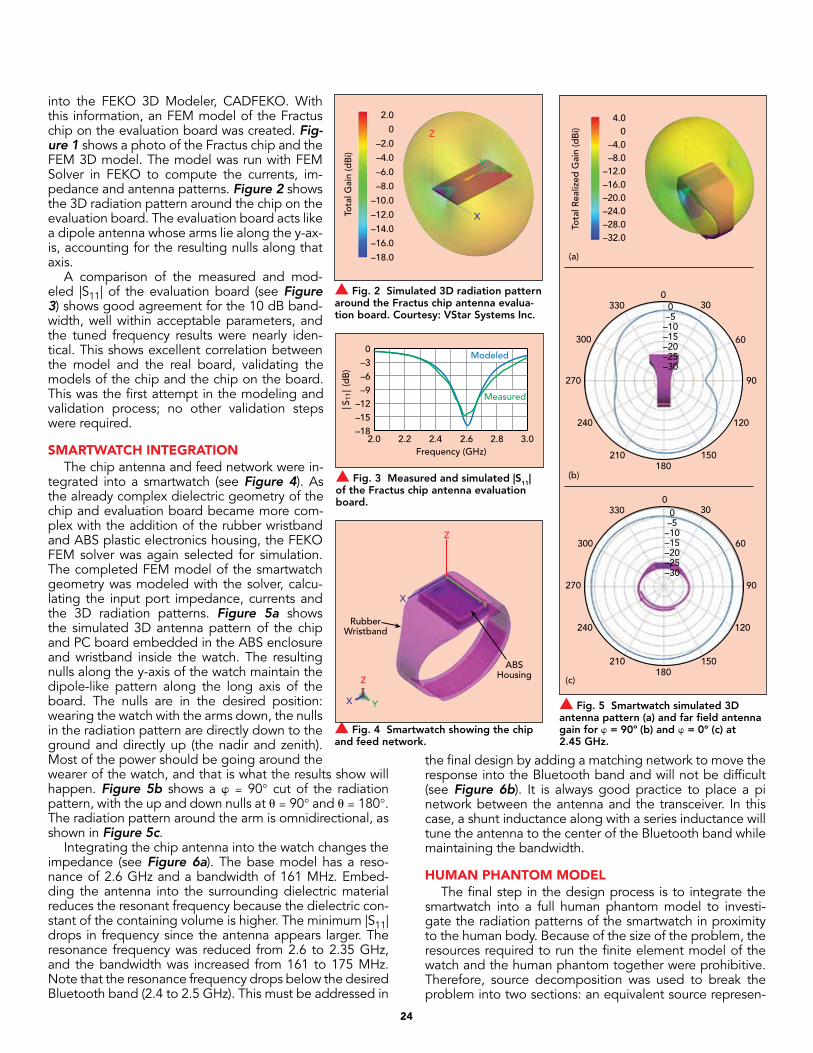
24
the final design by adding a matching network to move the response into the Bluetooth band and will not be difficult (see Figure 6b). It is always good practice to place a pi network between the antenna and the transceiver. In this case, a shunt inductance along with a series inductance will tune the antenna to the center of the Bluetooth band while maintaining the bandwidth.
HUMAN PHANTOM MODELThe final step in the design process is to integrate the
smartwatch into a full human phantom model to investi-gate the radiation patterns of the smartwatch in proximity to the human body. Because of the size of the problem, the resources required to run the finite element model of the watch and the human phantom together were prohibitive. Therefore, source decomposition was used to break the problem into two sections: an equivalent source represen-
into the FEKO 3D Modeler, CADFEKO. With this information, an FEM model of the Fractus chip on the evaluation board was created. Fig-ure 1 shows a photo of the Fractus chip and the FEM 3D model. The model was run with FEM Solver in FEKO to compute the currents, im-pedance and antenna patterns. Figure 2 shows the 3D radiation pattern around the chip on the evaluation board. The evaluation board acts like a dipole antenna whose arms lie along the y-ax-is, accounting for the resulting nulls along that axis.
A comparison of the measured and mod-eled |S11| of the evaluation board (see Figure 3) shows good agreement for the 10 dB band-width, well within acceptable parameters, and the tuned frequency results were nearly iden-tical. This shows excellent correlation between the model and the real board, validating the models of the chip and the chip on the board. This was the first attempt in the modeling and validation process; no other validation steps were required.
SMARTWATCH INTEGRATIONThe chip antenna and feed network were in-
tegrated into a smartwatch (see Figure 4). As the already complex dielectric geometry of the chip and evaluation board became more com-plex with the addition of the rubber wristband and ABS plastic electronics housing, the FEKO FEM solver was again selected for simulation. The completed FEM model of the smartwatch geometry was modeled with the solver, calcu-lating the input port impedance, currents and the 3D radiation patterns. Figure 5a shows the simulated 3D antenna pattern of the chip and PC board embedded in the ABS enclosure and wristband inside the watch. The resulting nulls along the y-axis of the watch maintain the dipole-like pattern along the long axis of the board. The nulls are in the desired position: wearing the watch with the arms down, the nulls in the radiation pattern are directly down to the ground and directly up (the nadir and zenith). Most of the power should be going around the wearer of the watch, and that is what the results show will happen. Figure 5b shows a φ = 90° cut of the radiation pattern, with the up and down nulls at θ = 90° and θ = 180°. The radiation pattern around the arm is omnidirectional, as shown in Figure 5c.
Integrating the chip antenna into the watch changes the impedance (see Figure 6a). The base model has a reso-nance of 2.6 GHz and a bandwidth of 161 MHz. Embed-ding the antenna into the surrounding dielectric material reduces the resonant frequency because the dielectric con-stant of the containing volume is higher. The minimum |S11| drops in frequency since the antenna appears larger. The resonance frequency was reduced from 2.6 to 2.35 GHz, and the bandwidth was increased from 161 to 175 MHz. Note that the resonance frequency drops below the desired Bluetooth band (2.4 to 2.5 GHz). This must be addressed in
s Fig. 2 Simulated 3D radiation pattern around the Fractus chip antenna evalua-tion board. Courtesy: VStar Systems Inc.
2.0
0
–2.0
–4.0
–6.0
–8.0
–10.0
–12.0
–14.0
–16.0
–18.0
X
Z
Y
Tota
l Gai
n (d
Bi)
s Fig. 5 Smartwatch simulated 3D antenna pattern (a) and far field antenna gain for φ = 90o (b) and φ = 0° (c) at 2.45 GHz.
4.00
–4.0–8.0
–12.0–16.0–20.0–24.0–28.0–32.0
0
180
330 30
60300
270
240
210 150
120
90
00–5
–10–15–20–25–30
0–5
–10–15–20–25–30
180
330 30
60300
270
240
210 150
120
90To
tal R
ealiz
ed G
ain
(dB
i)
(a)
(b)
(c)
s Fig. 4 Smartwatch showing the chip and feed network.
X
X
Z
Y
Y
Z
RubberWristband
ABSHousing
s Fig. 3 Measured and simulated |S11| of the Fractus chip antenna evaluation board.
0–3–6–9
–12–15–18
3.02.82.62.42.22.0Frequency (GHz)
Modeled
Measured
|S11
| (d
B)
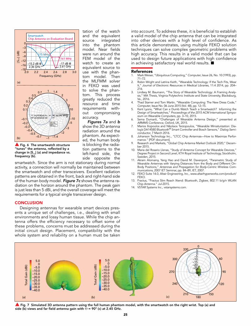
25
into account. To address these, it is beneficial to establish a valid model of the chip antenna that can be integrated into other devices with a high level of confidence. As this article demonstrates, using multiple FEKO solution techniques can solve complex geometric problems with high accuracy. This results in a valid model that can be used to design future applications with high confidence in achieving satisfactory real world results. n
References1. Mark Weiser, “Ubiquitous Computing,” Computer, Issue 26, No. 10 (1993), pp.
71–72.2. Robin Wright and Latrina Keith, “Wearable Technology: If the Tech Fits, Wear
It,” Journal of Electronic Resources in Medical Libraries, 11:4 2014, pp. 204–216.
3. Lindsey M. Baumann, “The Story of Wearable Technology: A Framing Analy-sis,” MA Thesis, Virginia Polytechnic Institute and State University, Blacksburg, Va., 2016.
4. Thad Starner and Tom Martin, “Wearable Computing: The New Dress Code,” Computer, Issue No. 06 June 2015 (Vol. 48), pp. 12–15.
5. Kent Lyons, “What Can a Dumb Watch Teach a Smartwatch? Informing the Design of Smartwatches,” Proceedings of the 2015 ACM International Sympo-sium on Wearable Computers, pp. 3–10, 2015.
6. Sema Dumanli, “Challenges of Wearable Antenna Design,” presented at ARMMS Conference, Oxford, UK, 2015.
7. Marios Iliopoulos and Nikolaos Terzopoulos, “Wearable Miniaturization: Dia-log’s DA14580 Bluetooth® Smart Controller and Bosch Sensors,” Dialog Semi-conductor, 7 March 2016.
8. Johanson Technology Inc., “LTCC Chip Antennas—How to Maximize Perfor-mance.” [PDF document].
9. Research and Markets, “Global Chip Antenna Market Outlook 2020,” Decem-ber 2015.
10. Maria del Rosario Llenas, “Study of Antenna Concept for Wearable Devices,” Degree Project in Second Level, KTH Royal Institute of Technology, Stockholm, Sweden, 2015.
11. Akram Alomainy, Yang Hao and David M. Davenport, “Parametric Study of Wearable Antennas with Varying Distances from the Body and Different On-Body Positions,” Antennas and Propagation for Body-Centric Wireless Com-munications, 2007 IET Seminar, pp. 84–89, IET, 2007.
12. FEKO Suite 14.0, Altair Engineering, Inc., www.altairhyperworks.com/product/FEKO.
13. Fractus, “Fractus Slim Reach Xtend: Bluetooth, Zigbee, 802.11 b/g/n WLAN Chip Antenna.” Jul-2015.
14. VSTAR Systems Inc., vstarsystems.com.
tation of the watch and the equivalent source integrated into the phantom model. Near fields were run around the FEM model of the watch to create an equivalent source to use with the phan-tom model. Then the MLFMM solver in FEKO was used to solve the phan-tom. This process greatly reduced the resource and time requirements with-out compromising accuracy.
Figures 7a and b show the 3D antenna radiation around the phantom. As expect-ed, the human body is blocking the radia-tion patterns to the left-hand side, the side opposite the
smartwatch. Since the arm is not stationary during normal activity, a connection will normally be maintained between the smartwatch and other transceivers. Excellent radiation patterns are obtained in the front, back and right-hand side of the human body model. Figure 7c shows the antenna ra-diation on the horizon around the phantom. The peak gain is just less than 5 dBi, and the overall coverage will meet the requirements for a typical single transceiver design.
CONCLUSIONDesigning antennas for wearable smart devices pres-
ents a unique set of challenges, i.e., dealing with small environments and lossy human tissue. While the chip an-tenna offers the efficiency necessary to offset some of these problems, concerns must be addressed during the initial circuit design. Placement, compatibility with the whole system and reliability on a human must be taken
s Fig. 6 The smartwatch structure “tunes” the antenna, reflected by a change in |S11| (a) and impedance vs. frequency (b).
–1
0
–3
–6
–9
–12
–16
–183.02.82.62.4
1 1.40.7
–1.4–2
20.5
30.4
–3
50.20.1
–0.1 0.1
0.2
0.3
0.4
0.5
0.7 1 2 3 5 101.4
–0.2–0.3
–0.4–0.5
–0.7
0.3
–5
10
–10
2.22.0Frequency (GHz)
(a)
(b)
–15.2 dB @2.36 GHz
–17 dB @2.61 GHz
SmartwatchChip Antenna on Evaluation Board
175 MHz161 MHz
|S11
| (d
B)
s Fig. 7 Simulated 3D antenna pattern using the full human phantom model, with the smartwatch on the right wrist. Top (a) and side (b) views and far field antenna gain with ϴ = 90° (c) at 2.45 GHz.
5.00
–5.0–10.0–15.0–20.0–25.0–30.0–35.0–40.0
5.00
–5.0–10.0–15.0–20.0–25.0–30.0–35.0–40.0
0 5 0 –5–10–15–20–25
180
330
210
30
150
60
120
90270
300
240
(a) (b) (c)
Tota
l Gai
n (d
Bi)
Tota
l Gai
n (d
Bi)

Enabling the Smart Home of the FutureQorvo’s Wi-Fi solutions offer the highest RF efficiency while delivering reliable coverage in the smallest form factor.
© Qorvo, Inc. | 2018. QORVO is a registered trademark of Qorvo, Inc. in the U.S. and in other countries.
Qorvo Wi-Fi solutions feature the latest BAW filters & iFEMs and offer the highest RF efficiency while delivering reliable coverage in the smallest form factor.Our solutions simplify the smart home, with Wi-Fi everywhere, and resolves Wi-Fi/LTE coexistence challenges. To learn more visit www.qorvo.com/cpe.
www.rfmw.com
For samples and orders, contact our
worldwide distributor.
www.qorvo.com
QPF4528 5 GHz Integrated FEM for Wi-Fi 802.11ax Systems
This integrated FEM has a compact form factor and integrated matching minimizes layout area in the application. Performance is focused on optimizing the PA for a 3.3 V supply voltage that reduces power consumption while maintaining the highest linear output power and leading edge throughput. Learn More.
QPF4528
27
https://www.qorvo.com/design-hub/blog/distributed-wifi-how-a-pod-in-every-room-enables-connected-smart-homes © 2018, Qorvo Inc.
1
Distributed Wi-Fi: How a Pod in Every Room Enables Connected Smart Homes
This article first appeared on the Qorvo Blog.
July 10, 2018
A distributed Wi-Fi indoor infrastructure — the next generation of Wi-Fi mesh — could change our vision of how we consider the smart home and its connections to the Internet of Things (IoT). In this blog post, we explain distributed Wi-Fi, some of its design challenges and how a “pod in every room” architecture can bring the connected smart home to life.
Design for IEEE 802.11ax to enable distributed Wi-Fi Everyone has experienced connectivity issues when multiple family members try to stream bandwidth-intensive videos or games on their devices at the same time. A truly connected smart home, with the capacity for various users and connected devices streaming simultaneously, is getting closer to reality. With the Wi-Fi IEEE 802.11ax standard expected to be released in 2019, it’s exciting to envision how our homes will have the capability and capacity for so much more, all connected wirelessly.
Although earlier versions of the Wi-Fi standard provided increased data rates, other challenges remained, including reliable range and avoiding interference. The Wi-Fi industry used multiple technologies, such as repeaters or power line extenders, to try to overcome these issues, but it appeared we couldn’t have it all — reliable range, high data rate and no interference. The capacity continued to be constrained.
Using a repeater inherently adds interference and can result in a poor user experience, even if it does minimally extend the range. Instead, we believe that distributing Wi-Fi or placing a pod in every room is a better approach to yield whole-home coverage. In short, you equip every room in a house with a pod that serves as a wireless access point. The pod connects to the router, which then connects to the internet.
IEEE 802.11ax will address the need for capacity, facilitating more efficient use of available bandwidth to carry more data. This will support these pods, creating worry-free connectivity — and a more efficient, distributed Wi-Fi indoor infrastructure for our smart homes. And families can then have the maximum data rate to run all apps at the same time.
Go in Depth Learn more about distributed Wi-Fi:
• How Upgrades to Distributed Wi-Fi Infrastructure Impact IoT Technologies
• Wi-Fi 802.11ax: What’s It All About?
• Where Is Wi-Fi Heading?
Distributed Wi-Fi: How a Pod in Every Room Enables Connected Smart Homes
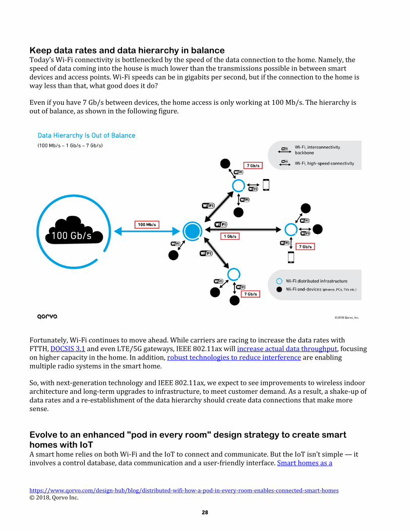
28
https://www.qorvo.com/design-hub/blog/distributed-wifi-how-a-pod-in-every-room-enables-connected-smart-homes © 2018, Qorvo Inc.
2
Keep data rates and data hierarchy in balance Today’s Wi-Fi connectivity is bottlenecked by the speed of the data connection to the home. Namely, the speed of data coming into the house is much lower than the transmissions possible in between smart devices and access points. Wi-Fi speeds can be in gigabits per second, but if the connection to the home is way less than that, what good does it do?
Even if you have 7 Gb/s between devices, the home access is only working at 100 Mb/s. The hierarchy is out of balance, as shown in the following figure.
Fortunately, Wi-Fi continues to move ahead. While carriers are racing to increase the data rates with FTTH, DOCSIS 3.1 and even LTE/5G gateways, IEEE 802.11ax will increase actual data throughput, focusing on higher capacity in the home. In addition, robust technologies to reduce interference are enabling multiple radio systems in the smart home.
So, with next-generation technology and IEEE 802.11ax, we expect to see improvements to wireless indoor architecture and long-term upgrades to infrastructure, to meet customer demand. As a result, a shake-up of data rates and a re-establishment of the data hierarchy should create data connections that make more sense.
Evolve to an enhanced "pod in every room" design strategy to create smart homes with IoT A smart home relies on both Wi-Fi and the IoT to connect and communicate. But the IoT isn’t simple — it involves a control database, data communication and a user-friendly interface. Smart homes as a
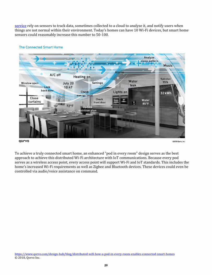
29
https://www.qorvo.com/design-hub/blog/distributed-wifi-how-a-pod-in-every-room-enables-connected-smart-homes © 2018, Qorvo Inc.
3
service rely on sensors to track data, sometimes collected to a cloud to analyze it, and notify users when things are not normal within their environment. Today’s homes can have 10 Wi-Fi devices, but smart home sensors could reasonably increase this number to 50-100.
To achieve a truly connected smart home, an enhanced “pod in every room” design serves as the best approach to achieve this distributed Wi-Fi architecture with IoT communications. Because every pod serves as a wireless access point, every access point will support Wi-Fi and IoT standards. This includes the home’s increased Wi-Fi requirements as well as Zigbee and Bluetooth devices. These devices could even be controlled via audio/voice assistance on command.
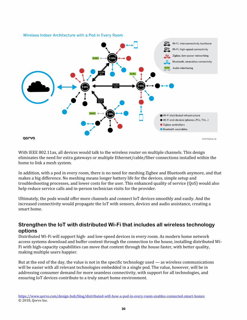
30
https://www.qorvo.com/design-hub/blog/distributed-wifi-how-a-pod-in-every-room-enables-connected-smart-homes © 2018, Qorvo Inc.
4
With IEEE 802.11ax, all devices would talk to the wireless router on multiple channels. This design eliminates the need for extra gateways or multiple Ethernet/cable/fiber connections installed within the home to link a mesh system.
In addition, with a pod in every room, there is no need for meshing Zigbee and Bluetooth anymore, and that makes a big difference. No meshing means longer battery life for the devices, simple setup and troubleshooting processes, and lower costs for the user. This enhanced quality of service (QoS) would also help reduce service calls and in-person technician visits for the provider.
Ultimately, the pods would offer more channels and connect IoT devices smoothly and easily. And the increased connectivity would propagate the IoT with sensors, devices and audio assistance, creating a smart home.
Strengthen the IoT with distributed Wi-Fi that includes all wireless technology options Distributed Wi-Fi will support high- and low-speed devices in every room. As modern home network access systems download and buffer content through the connection to the house, installing distributed Wi-Fi with high-capacity capabilities can move that content through the house faster, with better quality, making multiple users happier.
But at the end of the day, the value is not in the specific technology used — as wireless communications will be easier with all relevant technologies embedded in a single pod. The value, however, will be in addressing consumer demand for more seamless connectivity, with support for all technologies, and ensuring IoT devices contribute to a truly smart home environment.
31
https://www.qorvo.com/design-hub/blog/distributed-wifi-how-a-pod-in-every-room-enables-connected-smart-homes © 2018, Qorvo Inc.
5
Want to learn more about distributed Wi-Fi? Listen to our recorded webinar for more details, including standards, security, privacy and legislation.
About the Author Cees Links General Manager, Wireless Connectivity Business Unit
Cees Links (pronounced "Case") was the founder and CEO of GreenPeak Technologies, acquired by Qorvo in 2016. He is a pioneer of the wireless data industry, a visionary leader bringing the world of mobile computing and continuous networking together. In 2017, he was honored as a Wi-Fi pioneer with the Golden Mousetrap Lifetime Achievement Award by Design News.
QPQ1907 2.4 GHz Wi-Fi/BT/LTE Co-Existence BAW Filter
This high-performance, high-power BAW band-pass filter has extremely steep skirts and simultaneously exhibits low loss in the Wi-Fi band and high rejection in the 2.4 GHz bands. It is specifically designed to enable coexistence of Wi-Fi and
LTE signals within the same device or in close proximity to one another.
Learn More
Cees Links is a pioneer of the wireless data industry and the man who led the team that created and popularized Wi-Fi. Cees was the founder and CEO of GreenPeak Technologies, a Smart Home and IoT radio communications semiconductor company, now part of Qorvo. After Qorvo’s acqui-sition of GreenPeak in 2016, Cees has become the General Manager of the Wireless Connectivity business unit in Qorvo. He was recognized as Wi-Fi pioneer with the Golden Mousetrap Lifetime Achievement award.