introduction to plasma etching -...
TRANSCRIPT
Lam Research Corp. 1
Introduction to Plasma Etching
Dr. Steve SirardTechnical Director
Lam Research Corporation
Lam Research Corp. 2
► Pattern transfer requirements
► What is plasma and why is it needed?
► General plasma fundamentals
► Basic commercial etch hardware
► General plasma etch process fundamentals
► Specific case: Dielectric (SiO2, Si3N4, etc) etch mechanisms
Outline – Day 1

Lam Research Corp. 3
► Objective is to produce a
patterned thin film on a substrate
► Patterns are commonly formed by
either additive or subtractive
methods
► To pattern film, a mask is formed
with photolithography
▪ Resist pattern is a stencil that
protects underlying films/substrate
from dep or etch attack
► Supply etchant (either wet or
gaseous) to remove film in
undesired areas
► We will generally focus on the
subtractive process
Basic Pattern Transfer
Subtractive Additive
Mask
Substrate
Film

Lam Research Corp. 4
Wafer Fabrication Process Steps
Selectively
remove film to
define features
Residue/
Particle
Remove
photoresist
mask
Remove
residues and
particles
Photoresist
Create the
pattern
mask
Put down
the film to
be patterned
Deposit
next
materials
Segments Lam addresses
Etch Strip CleanLithographyDeposition DepositionIncoming
Wafer
Lam Research Corp. 5
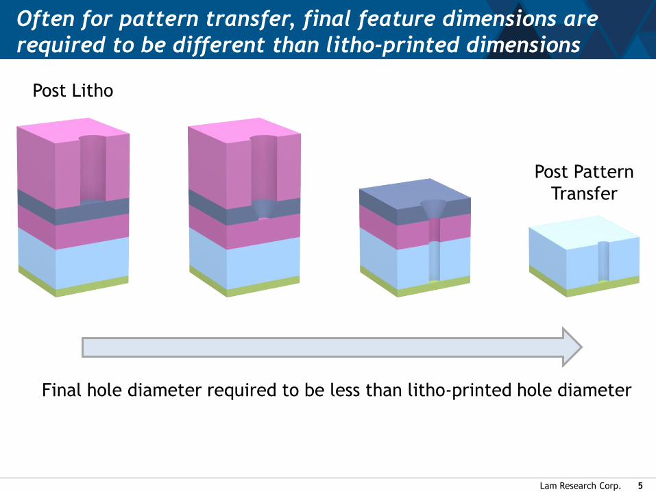
Often for pattern transfer, final feature dimensions are
required to be different than litho-printed dimensions
Final hole diameter required to be less than litho-printed hole diameter
Post Litho
Post Pattern
Transfer
Lam Research Corp. 6
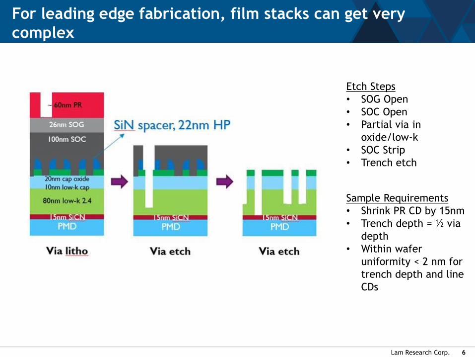
For leading edge fabrication, film stacks can get very
complex
Etch Steps
• SOG Open
• SOC Open
• Partial via in
oxide/low-k
• SOC Strip
• Trench etch
Sample Requirements
• Shrink PR CD by 15nm
• Trench depth = ½ via
depth
• Within wafer
uniformity < 2 nm for
trench depth and line
CDs
Lam Research Corp. 7
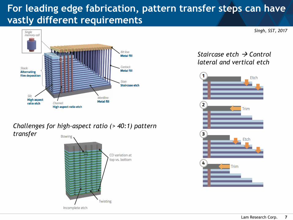
For leading edge fabrication, pattern transfer steps can have
vastly different requirementsSingh, SST, 2017
Challenges for high-aspect ratio (> 40:1) pattern
transfer
Staircase etch Control
lateral and vertical etch
Lam Research Corp. 8
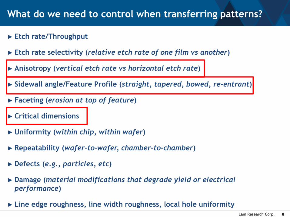
► Etch rate/Throughput
► Etch rate selectivity (relative etch rate of one film vs another)
► Anisotropy (vertical etch rate vs horizontal etch rate)
► Sidewall angle/Feature Profile (straight, tapered, bowed, re-entrant)
► Faceting (erosion at top of feature)
► Critical dimensions
► Uniformity (within chip, within wafer)
► Repeatability (wafer-to-wafer, chamber-to-chamber)
► Defects (e.g., particles, etc)
► Damage (material modifications that degrade yield or electrical
performance)
► Line edge roughness, line width roughness, local hole uniformity
What do we need to control when transferring patterns?
Lam Research Corp. 9
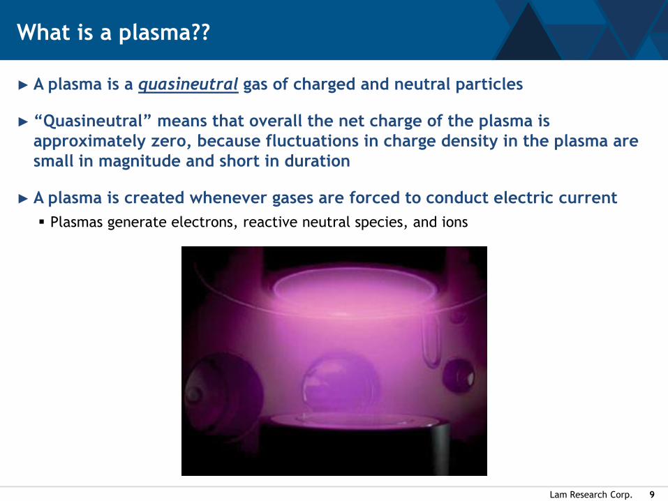
► A plasma is a quasineutral gas of charged and neutral particles
► “Quasineutral” means that overall the net charge of the plasma is
approximately zero, because fluctuations in charge density in the plasma are
small in magnitude and short in duration
► A plasma is created whenever gases are forced to conduct electric current
▪ Plasmas generate electrons, reactive neutral species, and ions
What is a plasma??
Lam Research Corp. 10
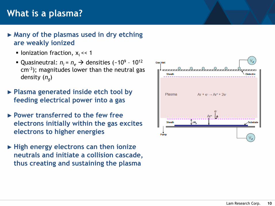
► Many of the plasmas used in dry etching
are weakly ionized
▪ Ionization fraction, xi << 1
▪ Quasineutral: ni = ne densities (~109 – 1012
cm-3); magnitudes lower than the neutral gas
density (ng)
► Plasma generated inside etch tool by
feeding electrical power into a gas
► Power transferred to the few free
electrons initially within the gas excites
electrons to higher energies
► High energy electrons can then ionize
neutrals and initiate a collision cascade,
thus creating and sustaining the plasma
What is a plasma?

Lam Research Corp. 11
► A plasma generates reactive species which are not available in a bottle and
“delivers” them to the substrate of interest
► Electrons are the main current-carriers because they are light and mobile
► Energy transfer between light electrons and gas molecules they collide with is
inefficient and electrons can attain a high average energy (thousands of
degrees above the gas temperature)
► Elevated electron temperature permits electron-molecule collisions to excite
high temperature type reactions (forming free radicals) in a low temperature
neutral gas
► Generating same reactive species without a plasma would require
temperatures in the 103 – 104 K range!
▪ These temperatures would incinerate organic photoresist and melt many inorganic films
What is a plasma?
Lam Research Corp. 12
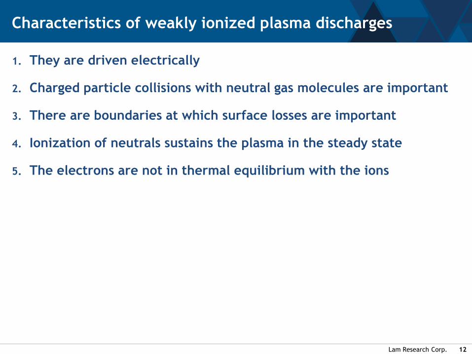
1. They are driven electrically
2. Charged particle collisions with neutral gas molecules are important
3. There are boundaries at which surface losses are important
4. Ionization of neutrals sustains the plasma in the steady state
5. The electrons are not in thermal equilibrium with the ions
Characteristics of weakly ionized plasma discharges

Lam Research Corp. 13
The Benefits of Plasma Processing (Etching and Deposition)
Lam Research Corp. 14
General Plasma Fundamentals
Lam Research Corp. 15
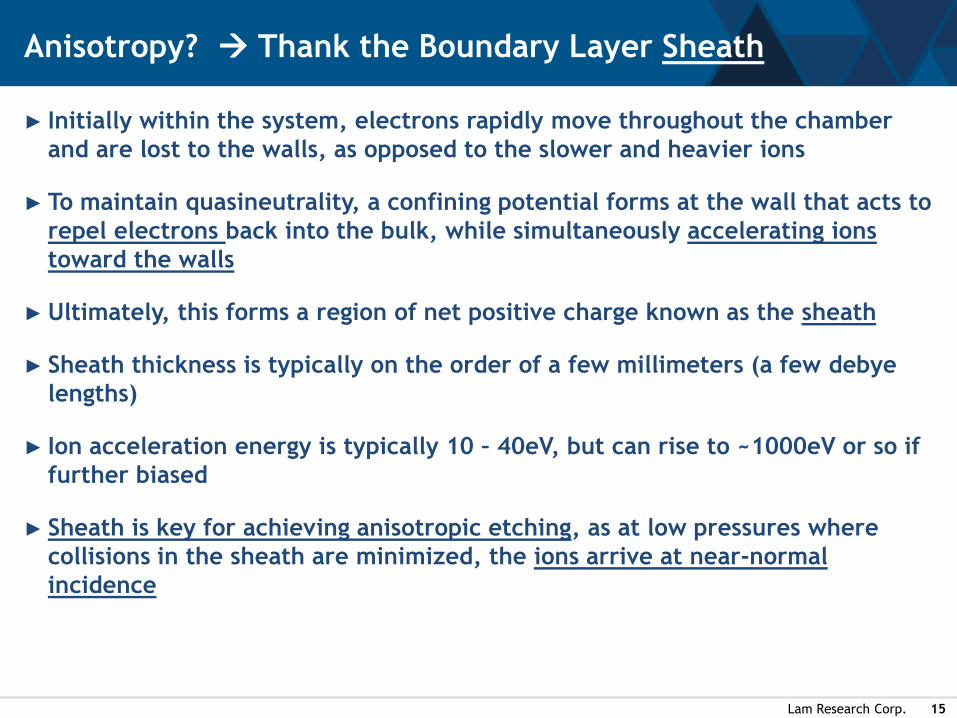
► Initially within the system, electrons rapidly move throughout the chamber
and are lost to the walls, as opposed to the slower and heavier ions
► To maintain quasineutrality, a confining potential forms at the wall that acts to
repel electrons back into the bulk, while simultaneously accelerating ions
toward the walls
► Ultimately, this forms a region of net positive charge known as the sheath
► Sheath thickness is typically on the order of a few millimeters (a few debye
lengths)
► Ion acceleration energy is typically 10 – 40eV, but can rise to ~1000eV or so if
further biased
► Sheath is key for achieving anisotropic etching, as at low pressures where
collisions in the sheath are minimized, the ions arrive at near-normal
incidence
Anisotropy? Thank the Boundary Layer Sheath
Lam Research Corp. 16
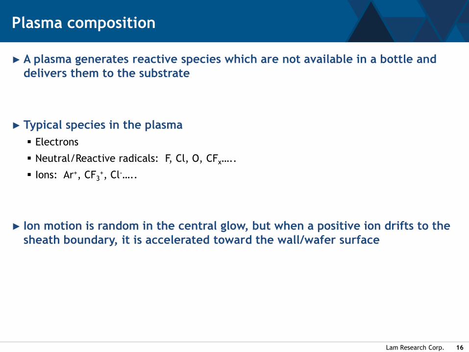
► A plasma generates reactive species which are not available in a bottle and
delivers them to the substrate
► Typical species in the plasma
▪ Electrons
▪ Neutral/Reactive radicals: F, Cl, O, CFx…..
▪ Ions: Ar+, CF3+, Cl-…..
► Ion motion is random in the central glow, but when a positive ion drifts to the
sheath boundary, it is accelerated toward the wall/wafer surface
Plasma composition

Lam Research Corp. 17
Silicon Etch
Si(s) + 4F(g) SiF4(g)
Classic experiment of Coburn and Winters - Alternately exposing Si surface to Molecular beam & ion beam
► Etch rate of combined is order of
magnitude higher than the sum of
individual rates SYNERGY!
► Shows how enhancement of the
etch requires energy of activation
which is provided by the ion
bombardment
Ion-Neutral synergy
Ions+Reactants have synergistic effect on etch rateKey mechanism for anisotropic etching

Lam Research Corp. 18
►Elastic collision:
▪When the internal energies of the two colliding particles do
not change—The energy exchange is restricted to kinetic energy
▪The sum of the kinetic energies is conserved
►Inelastic collision:
▪When the internal energies of the two colliding particles do
change—The sum of the kinetic energy is not conserved
Collisional processes in the plasma
Lam Research Corp. 19
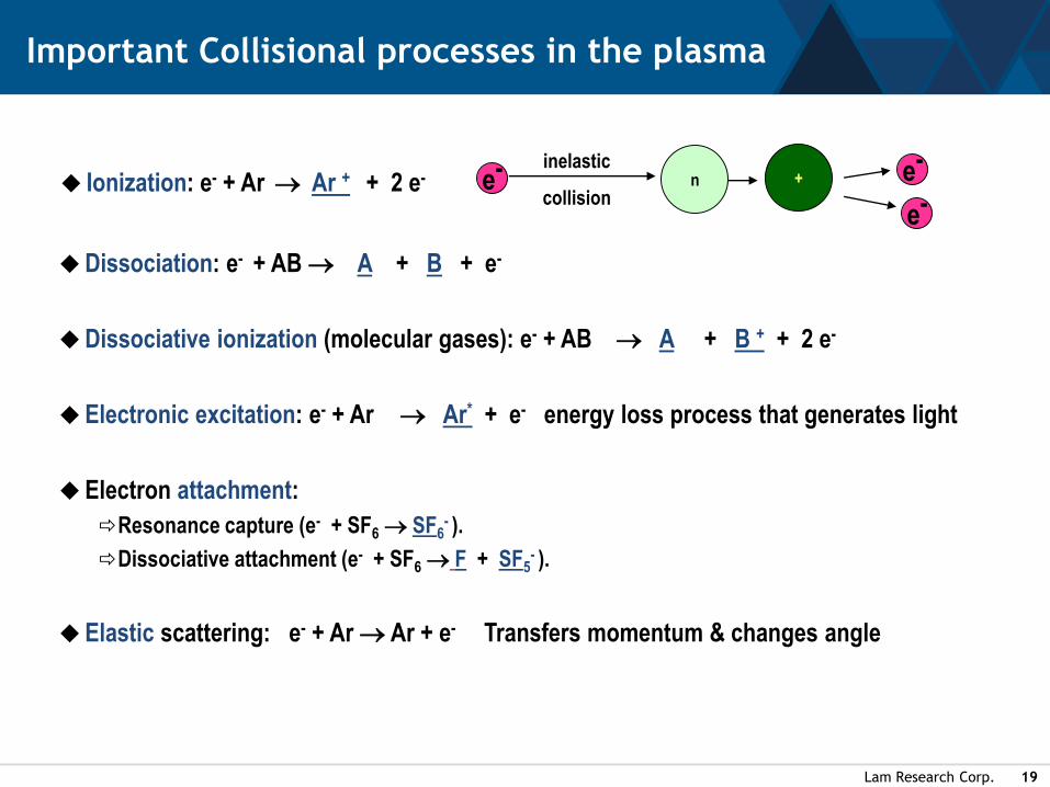
Important Collisional processes in the plasma
Dissociation: e- + AB A + B + e-
Dissociative ionization (molecular gases): e- + AB A + B + + 2 e-
Electronic excitation: e- + Ar Ar* + e- energy loss process that generates light
Electron attachment:
Resonance capture (e- + SF6 SF6- ).
Dissociative attachment (e- + SF6 F + SF5- ).
Elastic scattering: e- + Ar Ar + e- Transfers momentum & changes angle
n +inelastic
collisione-e-
e- Ionization: e- + Ar Ar + + 2 e-

Lam Research Corp. 20
►Ionization
Collisional processes in the plasma
CF4CF4+
inelastic
collision
e-
e-
e-
e- + CF4 CF4+ + 2 e-
An electron can ionize an atom or molecule if it has energy greater than
the ionization potential of the species
Lam Research Corp. 21
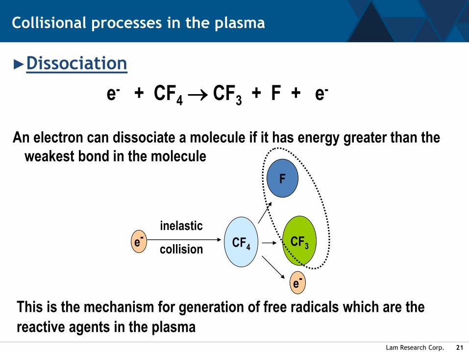
►Dissociation
Collisional processes in the plasma
e- + CF4 CF3 + F + e-
An electron can dissociate a molecule if it has energy greater than the
weakest bond in the molecule
e-
CF4CF3
inelastic
collisione-
F
This is the mechanism for generation of free radicals which are the
reactive agents in the plasma
Lam Research Corp. 22
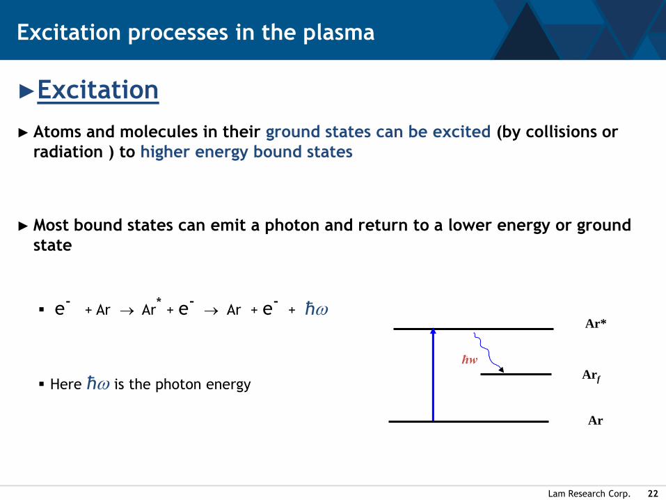
►Excitation
► Atoms and molecules in their ground states can be excited (by collisions or
radiation ) to higher energy bound states
► Most bound states can emit a photon and return to a lower energy or ground
state
▪ e-+ Ar Ar* + e-
Ar + e-+ ħw
▪ Here ħw is the photon energy
Excitation processes in the plasma
Ar*
ħw
Arf
Ar
Lam Research Corp. 23
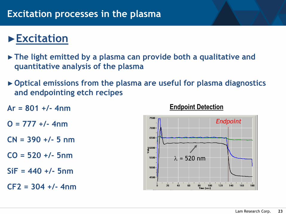
►Excitation
►The light emitted by a plasma can provide both a qualitative and
quantitative analysis of the plasma
►Optical emissions from the plasma are useful for plasma diagnostics
and endpointing etch recipes
Ar = 801 +/- 4nm
O = 777 +/- 4nm
CN = 390 +/- 5 nm
CO = 520 +/- 5nm
SiF = 440 +/- 5nm
CF2 = 304 +/- 4nm
Excitation processes in the plasma
Endpoint Detection
Endpoint
= 520 nm
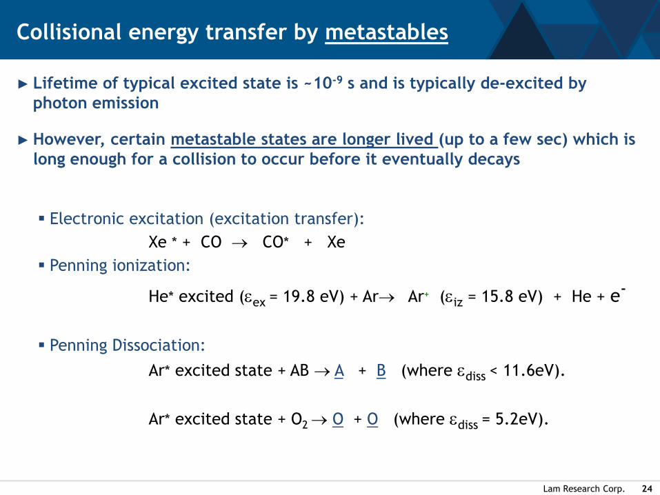
Lam Research Corp. 24
► Lifetime of typical excited state is ~10-9 s and is typically de-excited by
photon emission
► However, certain metastable states are longer lived (up to a few sec) which is
long enough for a collision to occur before it eventually decays
▪ Electronic excitation (excitation transfer):
Xe * + CO CO* + Xe
▪ Penning ionization:
He* excited (eex = 19.8 eV) + Ar Ar+ (eiz = 15.8 eV) + He + e-
▪ Penning Dissociation:
Ar* excited state + AB A + B (where ediss < 11.6eV).
Ar* excited state + O2 O + O (where ediss = 5.2eV).
Collisional energy transfer by metastables
Lam Research Corp. 25
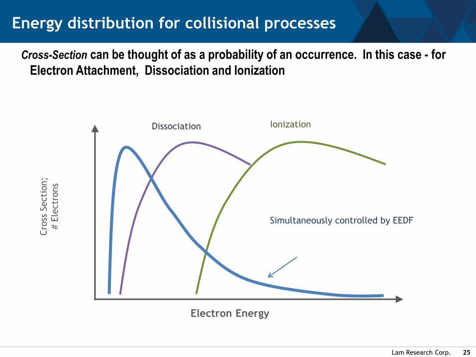
Energy distribution for collisional processes
Cross-Section can be thought of as a probability of an occurrence. In this case - for
Electron Attachment, Dissociation and Ionization
Ionization
Electron Energy
Cro
ss S
ecti
on;
# E
lectr
ons
Simultaneously controlled by EEDF
Dissociation
Lam Research Corp. 26
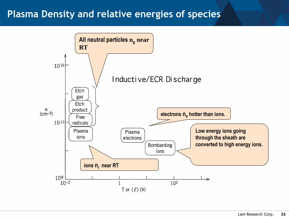
Plasma Density and relative energies of species
ions ni near RT
electrons ne hotter than ions.
All neutral particles ng near
RT
Low energy ions going
through the sheath are
converted to high energy ions.

Lam Research Corp. 27
Important Potentials
Lam Research Corp. 28
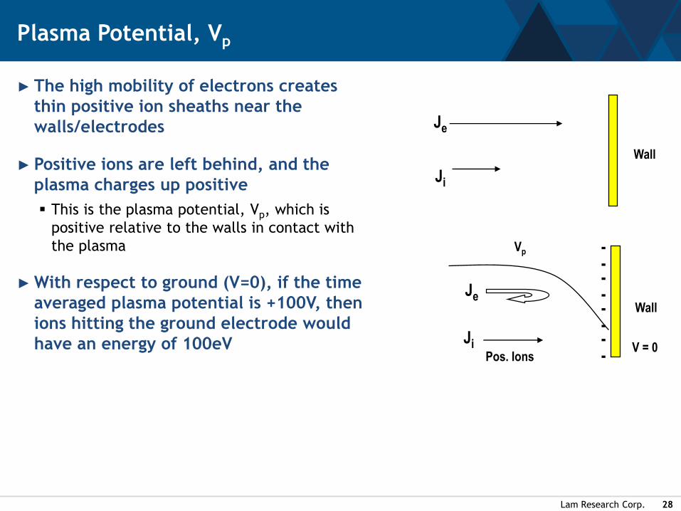
► The high mobility of electrons creates
thin positive ion sheaths near the
walls/electrodes
► Positive ions are left behind, and the
plasma charges up positive
▪ This is the plasma potential, Vp, which is
positive relative to the walls in contact with
the plasma
► With respect to ground (V=0), if the time
averaged plasma potential is +100V, then
ions hitting the ground electrode would
have an energy of 100eV
Plasma Potential, Vp
Je
Ji
Je
-
-
-
-
-
-
-
-Ji
Pos. Ions
Wall
V = 0
Vp
Wall
Lam Research Corp. 29
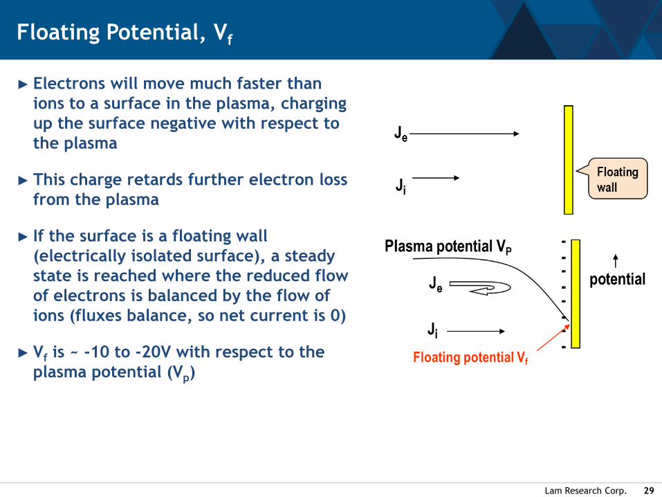
► Electrons will move much faster than
ions to a surface in the plasma, charging
up the surface negative with respect to
the plasma
► This charge retards further electron loss
from the plasma
► If the surface is a floating wall
(electrically isolated surface), a steady
state is reached where the reduced flow
of electrons is balanced by the flow of
ions (fluxes balance, so net current is 0)
► Vf is ~ -10 to -20V with respect to the
plasma potential (Vp)
Floating Potential, Vf
Lam Research Corp. 30
► Time-averaged value of the powered
electrode voltage is called the self-bias
voltage when measured with respect
to ground
► Vbias is negative with respect to the
plasma potential, Vp
► The potential drop across the sheath at
the powered electrode is the sum of
the plasma potential and the self-bias
▪ Vsh = Vp + IVbiasI
► The powered electrode will be
bombarded with much higher energy
ions than that of a grounded or floating
wall
Self-bias Voltage, Vbias
Bulk Plasma, Vp100V
85V
0V
-250V
Floating, Vf
Ground, V0
Powered Electrode, Vbias

Lam Research Corp. 31
► We’ve been discussing time-averaged potential behavior
► In actuality, the plasma (e.g., sheath potentials) are oscillating at the applied
RF frequency
► This has implications for the ion energy distribution (IED)
Ion energy distributions
Average
Plasma Potential Vp
DC bias potential Vbias0 20 40 60 80 100
0.000
0.005
0.010
0.015
IED
Ion Energy (eV)Ion Energy (eV)
Ion
Flu
x
At 5 mTorr, ie.
“collisionless”
Lam Research Corp. 32
RF excitation frequency has a big effect on the Ion Energy
Distribution Function
► Lower frequency
produces broader
distribution and
higher mean
energy
► Higher
frequencies
produce narrower
distribution and
lower mean
energies
► IEDF plays a key
role in modulating
etch behavior
0 100 200 300 400 500
400W 2MHz
(w/ 800W 60MHz)
400W 27MHz
400W 60MHz
400W 100MHz
Ion energy (eV)
Ion f
lux
400W 60 MHz
400W 27 MHz
400W 2 MHz / 800W 60MHz
400W 100 MHz
Lam Research Corp. 33
►Trends with increasing RF power (single frequency – 27MHz)
▪ Higher mean ion energy
▪ Wider IEDF
RF excitation frequency has a big effect on the Ion Energy
Distribution Function
0 100 200 300
Ion energy (eV)
ion flu
x (
mass 5
1)
0W 2MHz
27MHz power:
200W
400W
800W
1200W
1600W
2000W
400 W 27MHz
800 W 27MHz
1200 W 27MHz
2000 W 27MHz
Ion F
lux
Lam Research Corp. 34
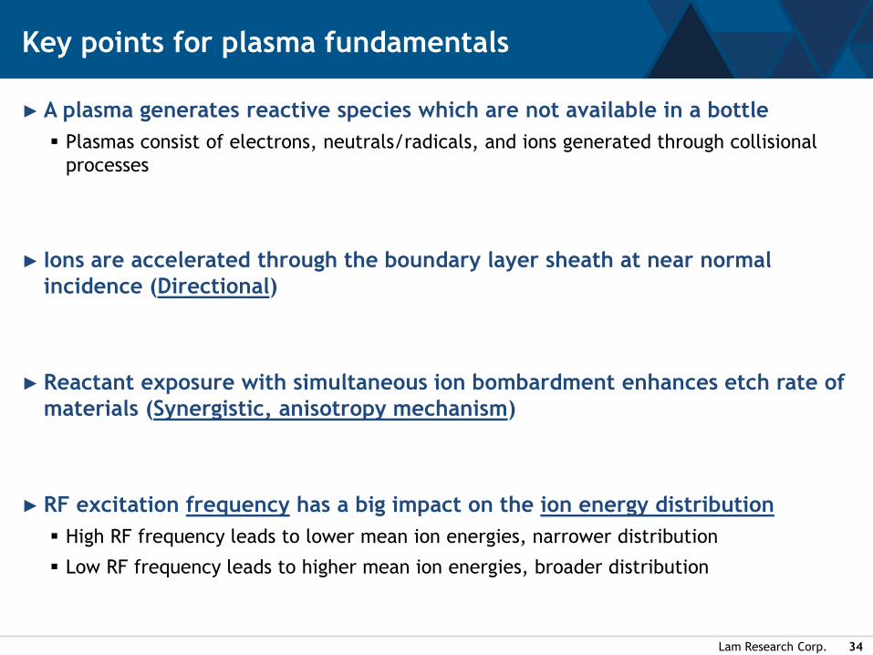
► A plasma generates reactive species which are not available in a bottle
▪ Plasmas consist of electrons, neutrals/radicals, and ions generated through collisional
processes
► Ions are accelerated through the boundary layer sheath at near normal
incidence (Directional)
► Reactant exposure with simultaneous ion bombardment enhances etch rate of
materials (Synergistic, anisotropy mechanism)
► RF excitation frequency has a big impact on the ion energy distribution
▪ High RF frequency leads to lower mean ion energies, narrower distribution
▪ Low RF frequency leads to higher mean ion energies, broader distribution
Key points for plasma fundamentals
Lam Research Corp. 35
Basic Commercial Etch Hardware
Lam Research ConfidentialSlide - 36
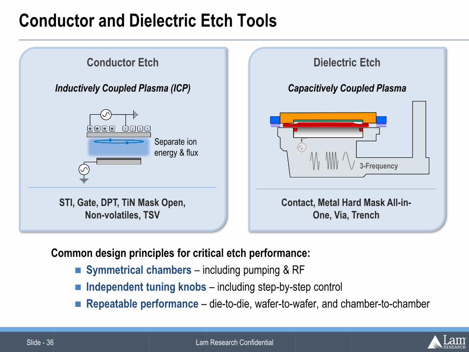
Conductor and Dielectric Etch Tools
Conductor Etch
Inductively Coupled Plasma (ICP)
Dielectric Etch
Capacitively Coupled Plasma
STI, Gate, DPT, TiN Mask Open,
Non-volatiles, TSV
Contact, Metal Hard Mask All-in-
One, Via, Trench
3-Frequency
Common design principles for critical etch performance:
Symmetrical chambers – including pumping & RF
Independent tuning knobs – including step-by-step control
Repeatable performance – die-to-die, wafer-to-wafer, and chamber-to-chamber
Separate ion
energy & flux
Lam Research Corp. 37
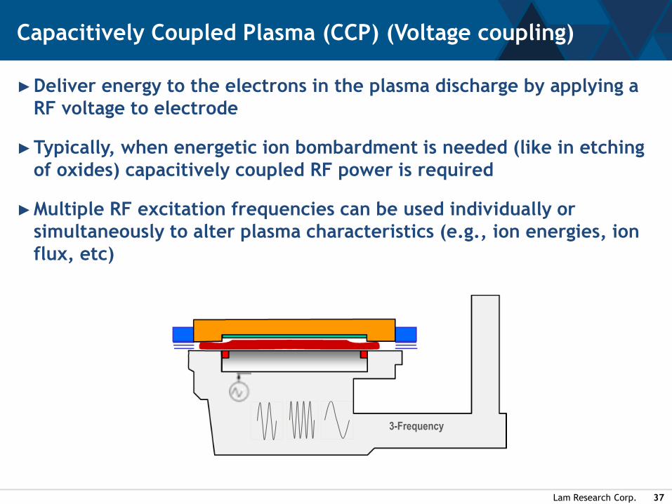
►Deliver energy to the electrons in the plasma discharge by applying a
RF voltage to electrode
►Typically, when energetic ion bombardment is needed (like in etching
of oxides) capacitively coupled RF power is required
►Multiple RF excitation frequencies can be used individually or
simultaneously to alter plasma characteristics (e.g., ion energies, ion
flux, etc)
Capacitively Coupled Plasma (CCP) (Voltage coupling)
3-Frequency
Lam Research Corp. 38
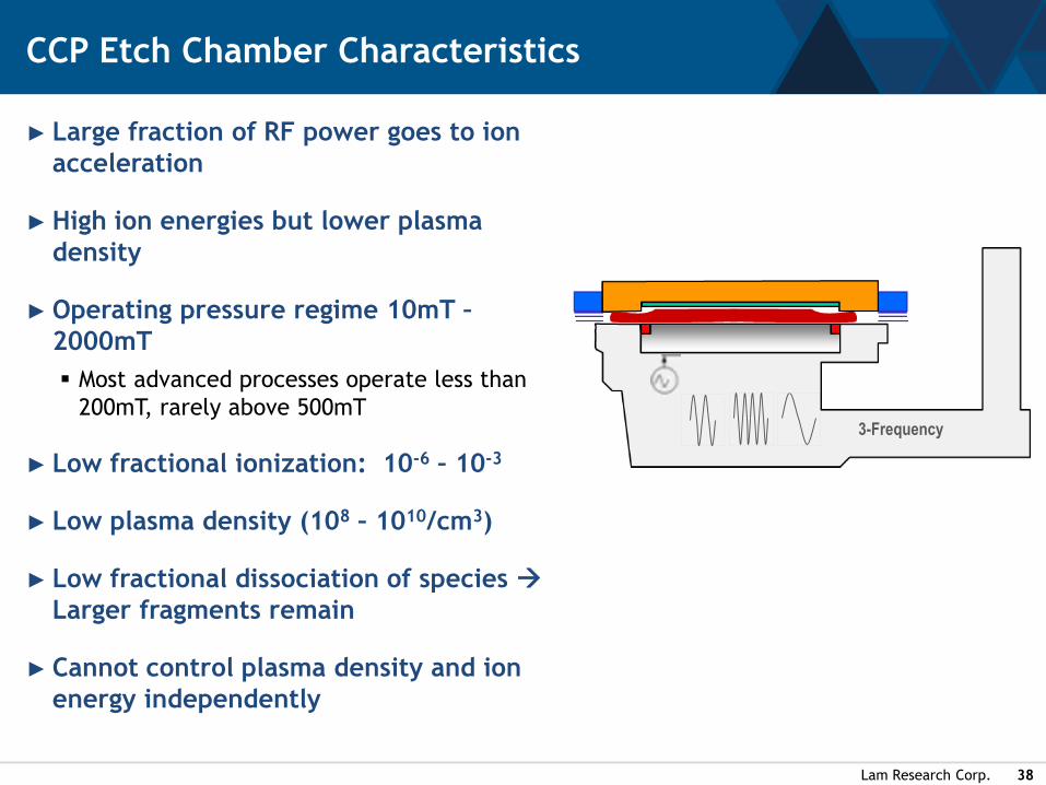
► Large fraction of RF power goes to ion
acceleration
► High ion energies but lower plasma
density
► Operating pressure regime 10mT –
2000mT
▪ Most advanced processes operate less than
200mT, rarely above 500mT
► Low fractional ionization: 10-6 – 10-3
► Low plasma density (108 – 1010/cm3)
► Low fractional dissociation of species
Larger fragments remain
► Cannot control plasma density and ion
energy independently
CCP Etch Chamber Characteristics
3-Frequency

Lam Research Corp. 39
► Inductive coupling is another commonly used method of delivering RF power
to the electrons in a plasma
► High RF current in the external coil generates an RF magnetic field in the
plasma region which, in turn, generates an RF electric field in the plasma
zone
▪ RF electric field can couple energy into the plasma electrons
► ICP tools generate high density plasmas and lower ion bombardment of
surfaces
Inductively Coupled Plasma (ICP) (Current Coupled)

Lam Research Corp. 40
► Generates large RF current as little power
is used for ion accelerations
▪ No high ion energy ion bombardment without
bias power
► With 2 RF generators, both plasma density
and ion energy can be controlled
independently
► Typical operating pressures 1 – 80 mT
► High fractional ionization (10-3 – 10-1)
► High plasma density (1011 – 1013)
► High fractional dissociation, smaller
fragments remain
► Larger gap to give required uniformity
ICP Etch Chamber Characteristics
Lam Research Corp. 41
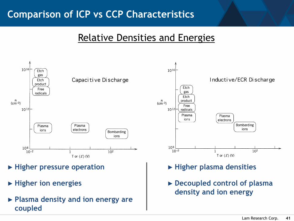
Comparison of ICP vs CCP Characteristics
Relative Densities and Energies
► Higher pressure operation
► Higher ion energies
► Plasma density and ion energy are
coupled
► Higher plasma densities
► Decoupled control of plasma
density and ion energy
Lam Research Corp. 42
Plasma Etch Process Fundamentals
Lam Research Corp. 43
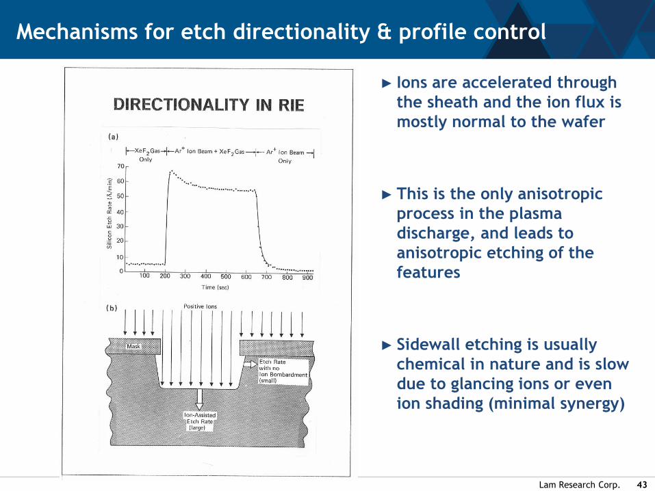
Mechanisms for etch directionality & profile control
► Ions are accelerated through
the sheath and the ion flux is
mostly normal to the wafer
► This is the only anisotropic
process in the plasma
discharge, and leads to
anisotropic etching of the
features
► Sidewall etching is usually
chemical in nature and is slow
due to glancing ions or even
ion shading (minimal synergy)
Lam Research Corp. 44
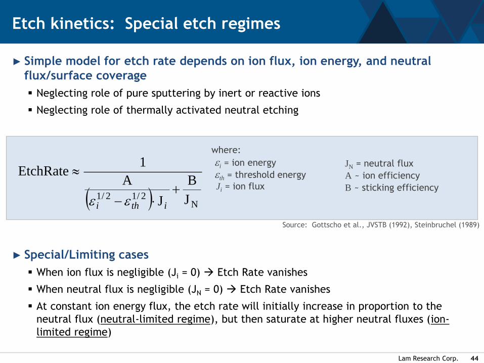
► Simple model for etch rate depends on ion flux, ion energy, and neutral
flux/surface coverage
▪ Neglecting role of pure sputtering by inert or reactive ions
▪ Neglecting role of thermally activated neutral etching
► Special/Limiting cases
▪ When ion flux is negligible (Ji = 0) Etch Rate vanishes
▪ When neutral flux is negligible (JN = 0) Etch Rate vanishes
▪ At constant ion energy flux, the etch rate will initially increase in proportion to the
neutral flux (neutral-limited regime), but then saturate at higher neutral fluxes (ion-
limited regime)
Etch kinetics: Special etch regimes
Source: Gottscho et al., JVSTB (1992), Steinbruchel (1989)
JN = neutral flux
A ~ ion efficiency
B ~ sticking efficiency
where:
ei = ion energy
eth = threshold energy
Ji = ion flux
N2/12/1 J
B
J
A
1EtchRate
ithi ee
Lam Research Corp. 45
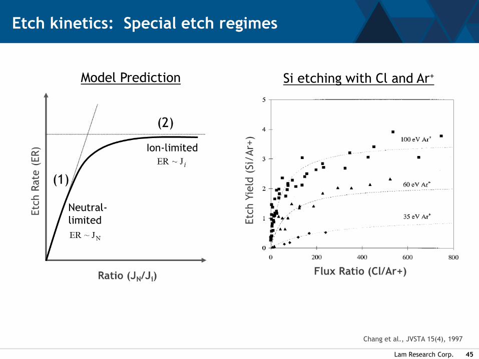
Etch kinetics: Special etch regimes
Model Prediction
Etc
h Y
ield
(Si/
Ar+
)
Flux Ratio (Cl/Ar+)
Chang et al., JVSTA 15(4), 1997
Si etching with Cl and Ar+
Lam Research Corp. 46
Mechanisms for etch directionality & profile control
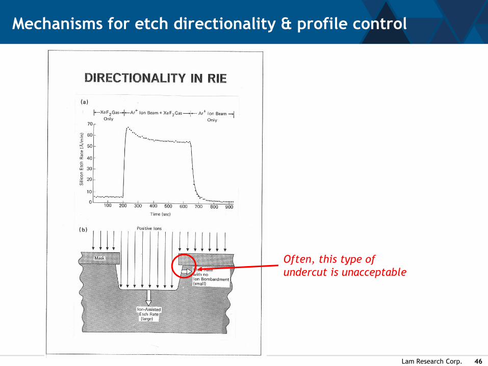
Often, this type of
undercut is unacceptable

Lam Research Corp. 47
► Condensable species
▪ Tend to form films on surfaces
▪ Very dependent on the surface temperature
► Reactive species
▪ Tend to react chemically with the surface
▪ Often saturate at one monolayer coverage
► Examples at room temperature
▪ Halogen atoms: Cl, F….. – reactive but not condensable
▪ Inert Gas atoms: Ar, Xe, He…. – not reactive or condensable
▪ Polymer Precursors (CxFy radicals): often both condensable and reactive
Mechanisms for etch directionality & profile control
Lam Research Corp. 48
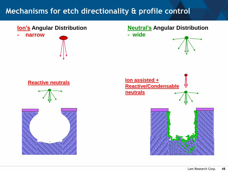
Mechanisms for etch directionality & profile control
Ion’s Angular Distribution
- narrow
Neutral’s Angular Distribution
- wide
Reactive neutralsIon assisted +
Reactive/Condensable
neutrals
Lam Research Corp. 49
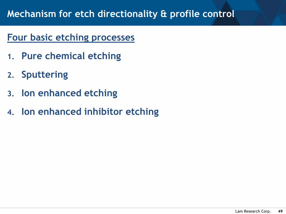
Four basic etching processes
1. Pure chemical etching
2. Sputtering
3. Ion enhanced etching
4. Ion enhanced inhibitor etching
Mechanism for etch directionality & profile control
Lam Research Corp. 50
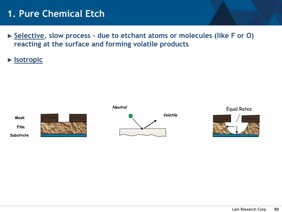
► Selective, slow process - due to etchant atoms or molecules (like F or O)
reacting at the surface and forming volatile products
► Isotropic
1. Pure Chemical Etch
Mask
Substrate
Film
Equal RatesNeutral
Volatile

Lam Research Corp. 51
► Non-selective, slow - physical process due to energetic ion bombardment
ejecting surface atoms
► Anisotropic
2. Sputtering
Mask
Substrate
Film
Ion
Involatile
Lam Research Corp. 52
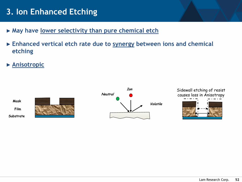
► May have lower selectivity than pure chemical etch
► Enhanced vertical etch rate due to synergy between ions and chemical
etching
► Anisotropic
3. Ion Enhanced Etching
Mask
Substrate
Film
Neutral
Ion
Volatile
Sidewall etching of resistcauses loss in Anisotropy

Lam Research Corp. 53
► Similar to ion enhanced etching, but may have higher selectivity
► Inhibitor (e.g., polymer film) deposited on the sidewalls where ions are not
effective at removing
► Anisotropic
4. Ion Enhanced Inhibitor Etching
Mask
Substrate
Film
NeutralIon
VolatilePassivation film
Film removed
Lam Research Corp. 54
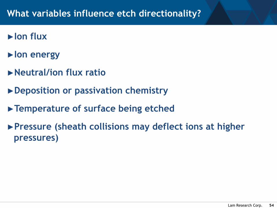
►Ion flux
►Ion energy
►Neutral/ion flux ratio
►Deposition or passivation chemistry
►Temperature of surface being etched
►Pressure (sheath collisions may deflect ions at higher
pressures)
What variables influence etch directionality?
Lam Research Corp. 55
Dielectric Etch Mechanisms
Lam Research Corp. 56
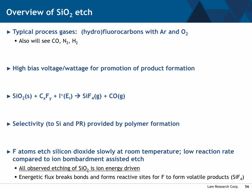
► Typical process gases: (hydro)fluorocarbons with Ar and O2
▪ Also will see CO, N2, H2
► High bias voltage/wattage for promotion of product formation
► SiO2(s) + CxFy + I+(Ei) SiF4(g) + CO(g)
► Selectivity (to Si and PR) provided by polymer formation
► F atoms etch silicon dioxide slowly at room temperature; low reaction rate
compared to ion bombardment assisted etch
▪ All observed etching of SiO2 is ion energy driven
▪ Energetic flux breaks bonds and forms reactive sites for F to form volatile products (SiF4)
Overview of SiO2 etch
Lam Research Corp. 57
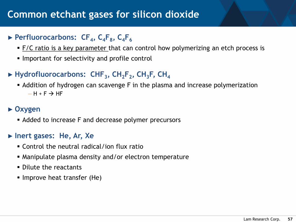
► Perfluorocarbons: CF4, C4F8, C4F6
▪ F/C ratio is a key parameter that can control how polymerizing an etch process is
▪ Important for selectivity and profile control
► Hydrofluorocarbons: CHF3, CH2F2, CH3F, CH4
▪ Addition of hydrogen can scavenge F in the plasma and increase polymerization
— H + F HF
► Oxygen
▪ Added to increase F and decrease polymer precursors
► Inert gases: He, Ar, Xe
▪ Control the neutral radical/ion flux ratio
▪ Manipulate plasma density and/or electron temperature
▪ Dilute the reactants
▪ Improve heat transfer (He)
Common etchant gases for silicon dioxide
Lam Research Corp. 58
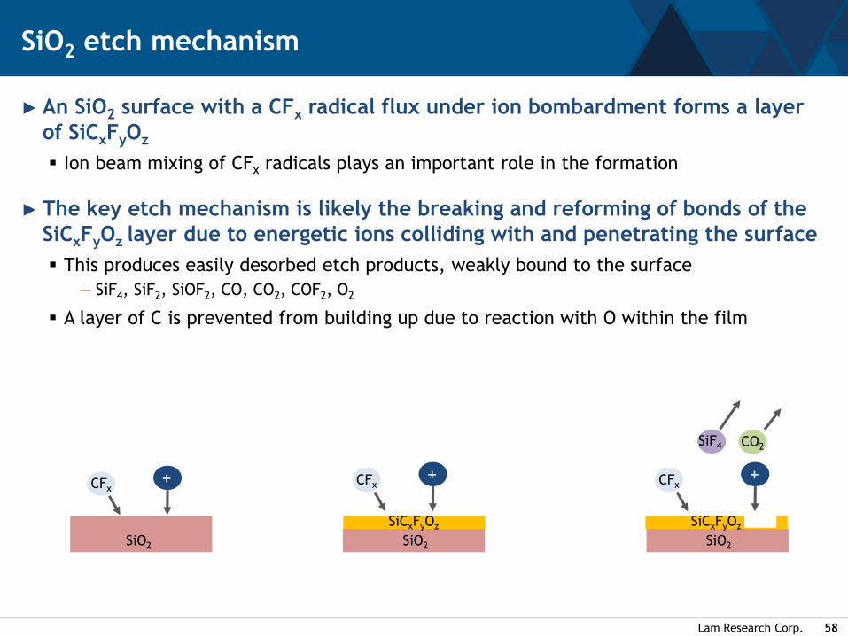
► An SiO2 surface with a CFx radical flux under ion bombardment forms a layer
of SiCxFyOz
▪ Ion beam mixing of CFx radicals plays an important role in the formation
► The key etch mechanism is likely the breaking and reforming of bonds of the
SiCxFyOz layer due to energetic ions colliding with and penetrating the surface
▪ This produces easily desorbed etch products, weakly bound to the surface
— SiF4, SiF2, SiOF2, CO, CO2, COF2, O2
▪ A layer of C is prevented from building up due to reaction with O within the film
SiO2 etch mechanism
CFx+ CFx
+
SiCxFyOz
SiO2SiO2 SiO2
CFx+
SiCxFyOz
CO2SiF4
Lam Research Corp. 59
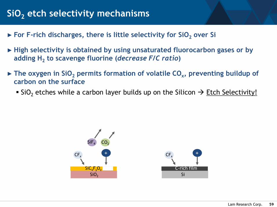
► For F-rich discharges, there is little selectivity for SiO2 over Si
► High selectivity is obtained by using unsaturated fluorocarbon gases or by
adding H2 to scavenge fluorine (decrease F/C ratio)
► The oxygen in SiO2 permits formation of volatile COx, preventing buildup of
carbon on the surface
▪ SiO2 etches while a carbon layer builds up on the Silicon Etch Selectivity!
SiO2 etch selectivity mechanisms
SiO2
CFx+
SiCxFyOz
CO2SiF4
Si
CFx+
C-rich film
Lam Research Corp. 60
►Addition of oxygen can increase photoresist etch rate, thereby
decreasing oxide etch selectivity to resist
► If the etch is more polymerizing (i.e., low F/C ratio), then oxygen
addition will increase the oxide etch rate without as large an increase
in the resist etch rate (thus, increasing selectivity)
▪ Due to additional oxygen liberated by SiO2 as it is etched
Effect of Oxygen

Lam Research Corp. 61
► If the plasma is made too fluorine deficient, polymer deposition will dominate
over etching of SiO2 Etch Stop!
▪ The F/C ratio where this occurs is dependent on energetic ion flux
▪ At higher energies, etching will take place
▪ At lower energies, deposition will take place
► For high selectivity, we often have to operate close to this boundary
Fluorine/Carbon ratio
F/C Ratio
Bia
s (V
)
Etching
Polymerization
Lam Research Corp. 62
► Mechanistically not as well understood as Si or SiO2 etching
► Often said that Si3N4 etch behavior is in between Si and SiO2
▪ Relative reactivity to F atoms without ion bombardment is in between Si and SiO2
▪ The effectiveness in removing polymeric blocking material is in between Si and SiO2
► SiF4 is the dominant Si-containing etch product
► How is nitrogen evolved?
▪ In pure Fluorine plasma (F atoms only), nitrogen leaves as N2
▪ When nitride is etched in a fluorocarbon plasma, optical emission from the CN radical is
observed (FCN has been observed in such situations)
Etching Si3N4

Lam Research Corp. 63
► SiO2/Si3N4 and Si3N4/Si selective etching can be obtained with fluorine-
deficient fluorocarbon plasmas such as CF4/H2, CHF3, C4F8, etc
► The mechanism responsible for SiO2/Si3N4 selective etching is similar to that
discussed previously for SiO2/Si etching
► For SiO2/Si3N4 selective etching, the key factor is that nitrogen is less efficient
than oxygen in removing carbon
▪ Therefore, conditions can be found where SiO2 etches and Si3N4 does not
Nitride etching selectivity