introduction to electronics and semiconductorinc.kmutt.ac.th/course/inc223/inc223 lecture1...
TRANSCRIPT
1
Introduction to Electronicsand Semiconductor

2
Chapter Objectives
• To study and understand basic electronics.
• To study and understand semiconductor principles.
3
Definition
Electronics is the branch of science and technology that deals with electrical circuits involving active electrical components such as vacuum tubes, transistors, diodes and integrated circuits.
Nowadays, most electronic devices use semiconductor components to perform electron control. The study of semiconductor devices and related technology is considered a branch of solid state physics, whereas the design and construction of electronic circuits to solve practical problems come under electronics engineering.
4
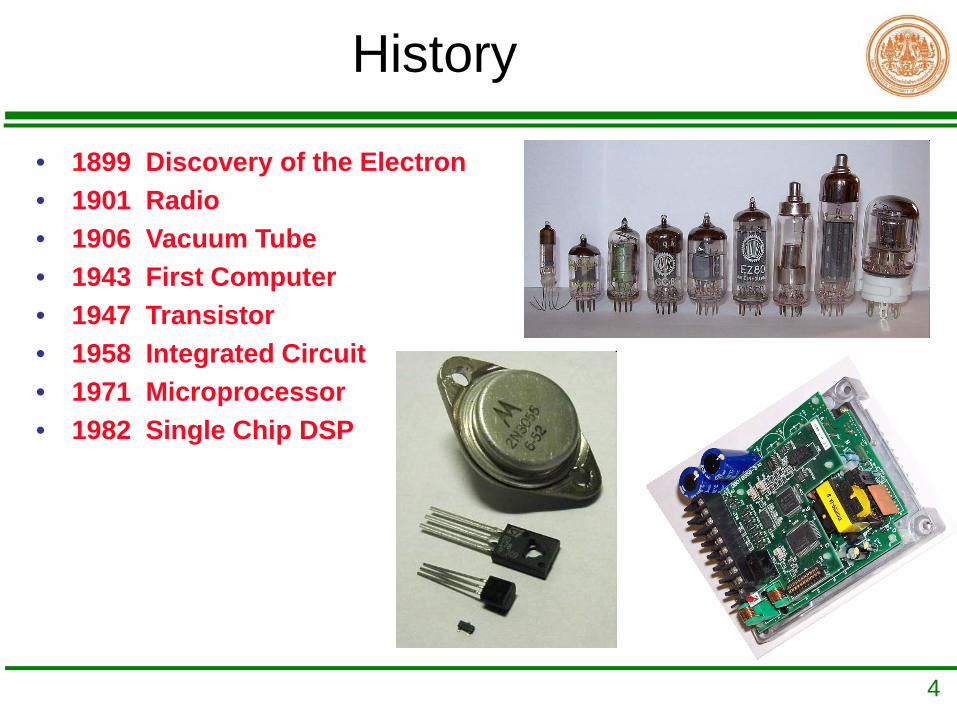
History
• 1899 Discovery of the Electron• 1901 Radio• 1906 Vacuum Tube• 1943 First Computer• 1947 Transistor• 1958 Integrated Circuit• 1971 Microprocessor• 1982 Single Chip DSP

5
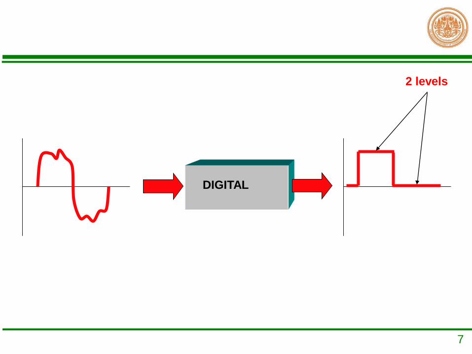
Analog vs Digital
• The world of electronics can be divided into digital or analog.
• Analog signals come from nature and from physical systems.
• Analog signals have an infinite variety of levels.
• Digital signals usually have only two levels.
• Digital signals are often represented as binary numbers.
• A/D and D/A conversions are commonplace.

6
ANALOG
An infinite number of levels
7
DIGITAL
2 levels
8
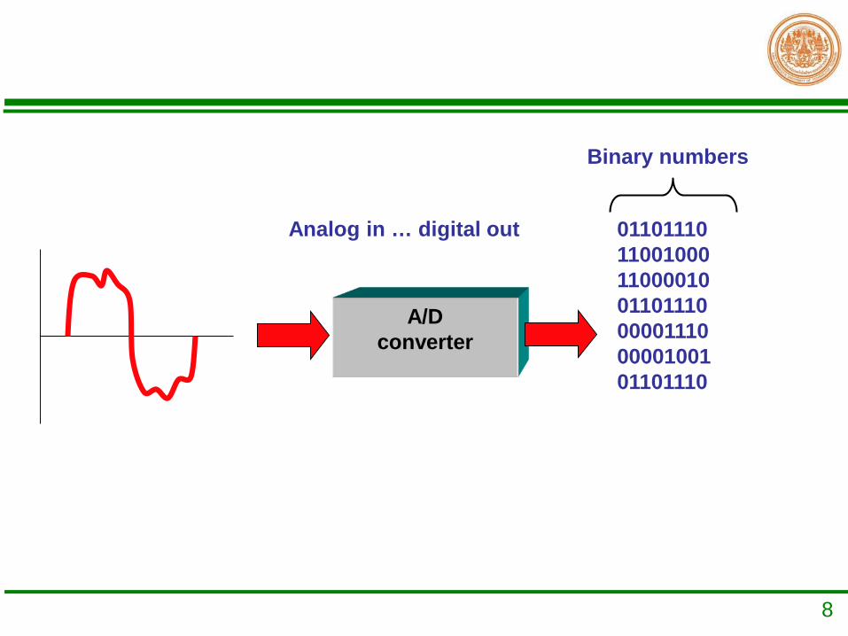
A/Dconverter
01101110110010001100001001101110000011100000100101101110
Binary numbers
Analog in … digital out
9
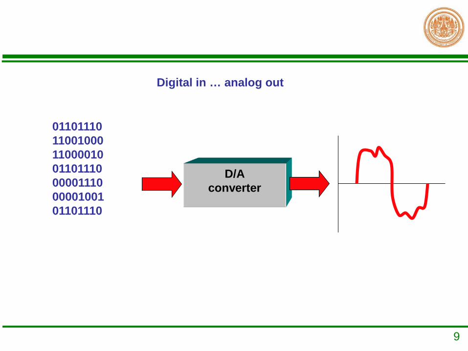
D/Aconverter
01101110110010001100001001101110000011100000100101101110
Digital in … analog out
10
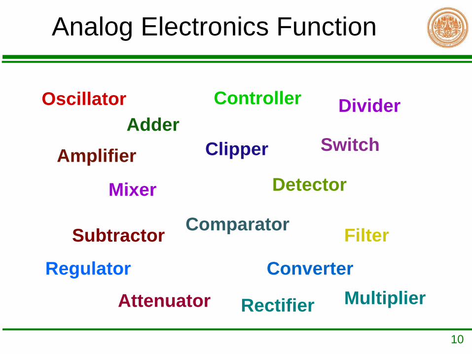
Analog Electronics Function
Adder
Subtractor
Attenuator
Clipper
Comparator
Controller
Converter
Detector
Divider
Filter
Mixer
Multiplier
Oscillator
Rectifier
Regulator
SwitchAmplifier
11
Concept Preview
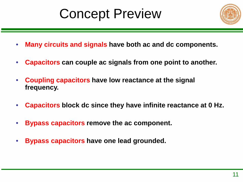
• Many circuits and signals have both ac and dc components.
• Capacitors can couple ac signals from one point to another.
• Coupling capacitors have low reactance at the signal frequency.
• Capacitors block dc since they have infinite reactance at 0 Hz.
• Bypass capacitors remove the ac component.
• Bypass capacitors have one lead grounded.
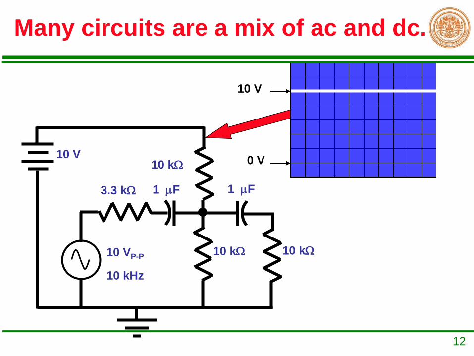
12
10 V
0 V10 V
10 VP-P
10 kHz
10 kΩ 10 kΩ
10 kΩ
3.3 kΩ 1 µF 1 µF
Many circuits are a mix of ac and dc.

13
+5 V
0 V
-5 V10 V
10 VP-P
10 kHz
10 kΩ 10 kΩ
10 kΩ
3.3 kΩ 1 µF 1 µF

14
0 V
10 V
10 VP-P
10 kHz
10 kΩ 10 kΩ
10 kΩ
3.3 kΩ 1 µF 1 µF
Note the loss in ac amplitude due to the drop across
the 3.3 kΩ resistor.

15
+5 V
0 V
10 V
10 VP-P
10 kHz
10 kΩ 10 kΩ
10 kΩ
3.3 kΩ 1 µF 1 µF
Note the combineddc and ac.
16
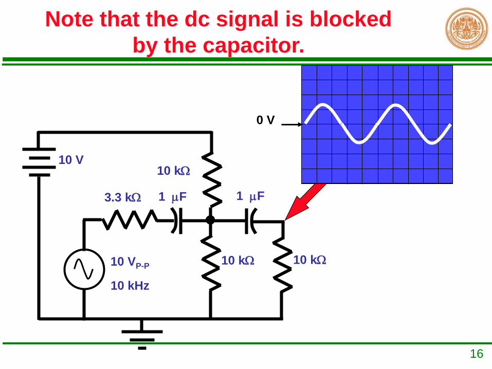
0 V
10 V
10 VP-P
10 kHz
10 kΩ 10 kΩ
10 kΩ
3.3 kΩ 1 µF 1 µF
Note that the dc signal is blockedby the capacitor.
17
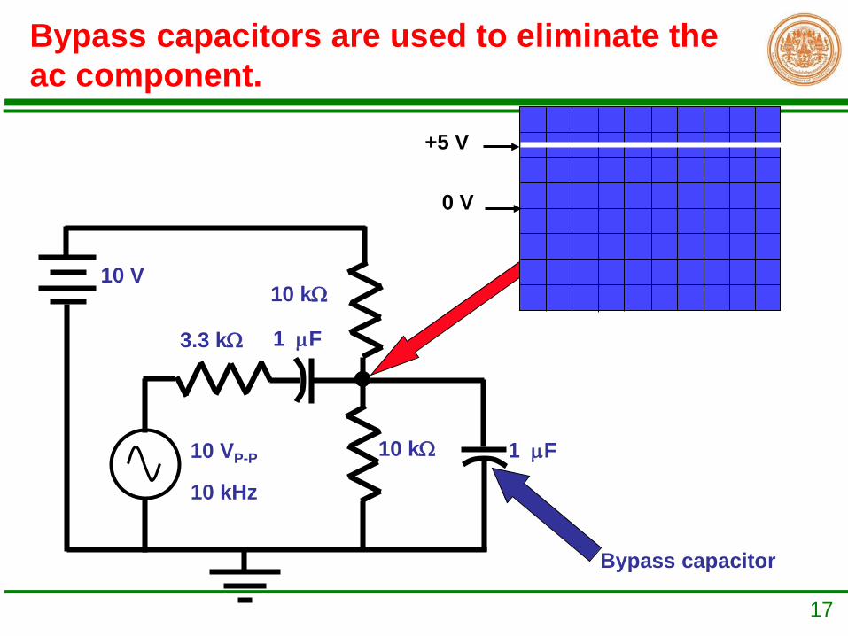
+5 V
0 V
10 V
10 VP-P
10 kHz
10 kΩ
10 kΩ
3.3 kΩ 1 µF
1 µF
Bypass capacitor
Bypass capacitors are used to eliminate the ac component.

18
Through-hole soldering
Solder
Device leads pass through holes in the circuit board.
19
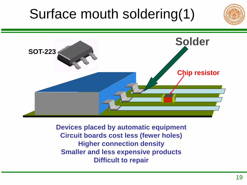
Surface mouth soldering(1)
Devices placed by automatic equipmentCircuit boards cost less (fewer holes)
Higher connection densitySmaller and less expensive products
Difficult to repair
SOT-223
Chip resistor
Solder

20
Surface mouth soldering(2)
21
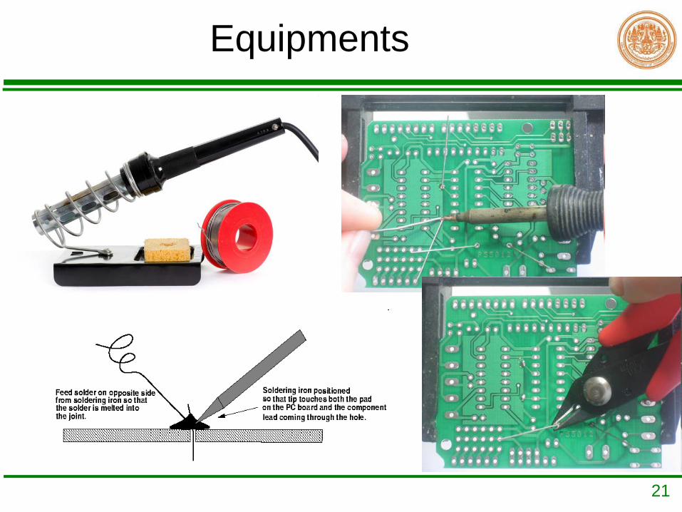
Equipments
22
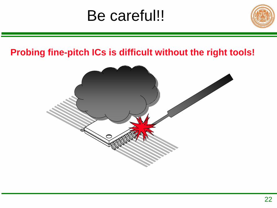
Be careful!!
Probing fine-pitch ICs is difficult without the right tools!
23
Semiconductor
• A semiconductor is a material with electrical conductivity due to electron flow (as opposed to ionic conductivity) intermediate in magnitude between that of a conductor and an insulator.
• Semiconductor materials are the foundation of modern electronics, including radio, computers, telephones, and many other devices.
• Such devices include transistors, solar cells, many kinds of diodes including the light-emitting diode, the silicon controlled rectifier, and digital and analog integrated circuits.

24
Contents
• Conductors and Insulators• Semiconductors• N-type Semiconductors• P-type Semiconductors• Majority and Minority Carriers

25
Energy Diagram
26
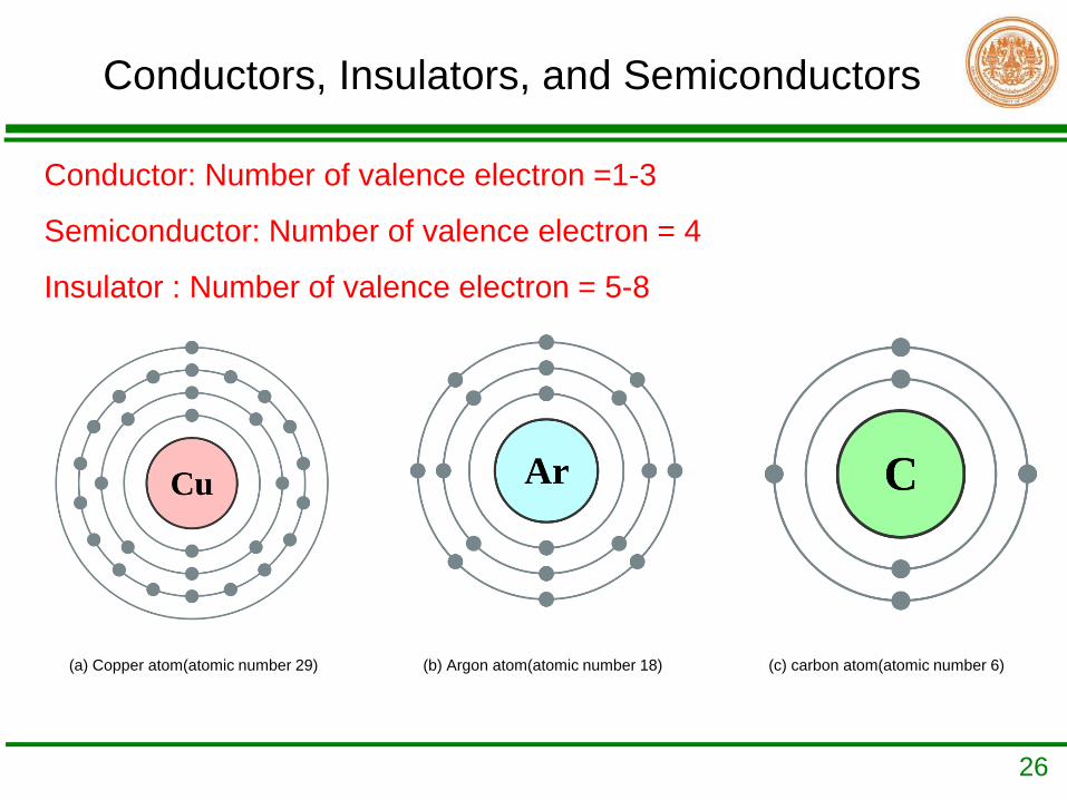
Conductor: Number of valence electron =1-3
Semiconductor: Number of valence electron = 4
Insulator : Number of valence electron = 5-8
Conductors, Insulators, and Semiconductors
(c) carbon atom(atomic number 6)(a) Copper atom(atomic number 29) (b) Argon atom(atomic number 18)
27
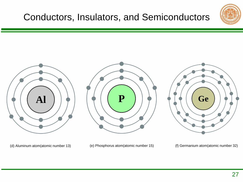
Conductors, Insulators, and Semiconductors
(f) Germanium atom(atomic number 32)(d) Aluminum atom(atomic number 13) (e) Phosphorus atom(atomic number 15)
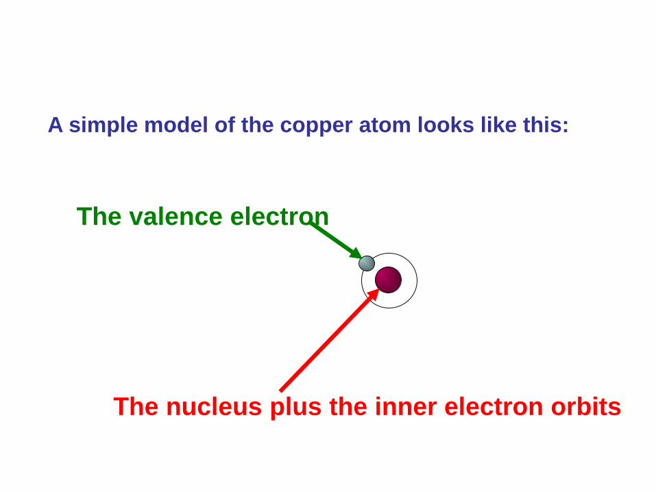
The valence electron
The nucleus plus the inner electron orbits
A simple model of the copper atom looks like this:
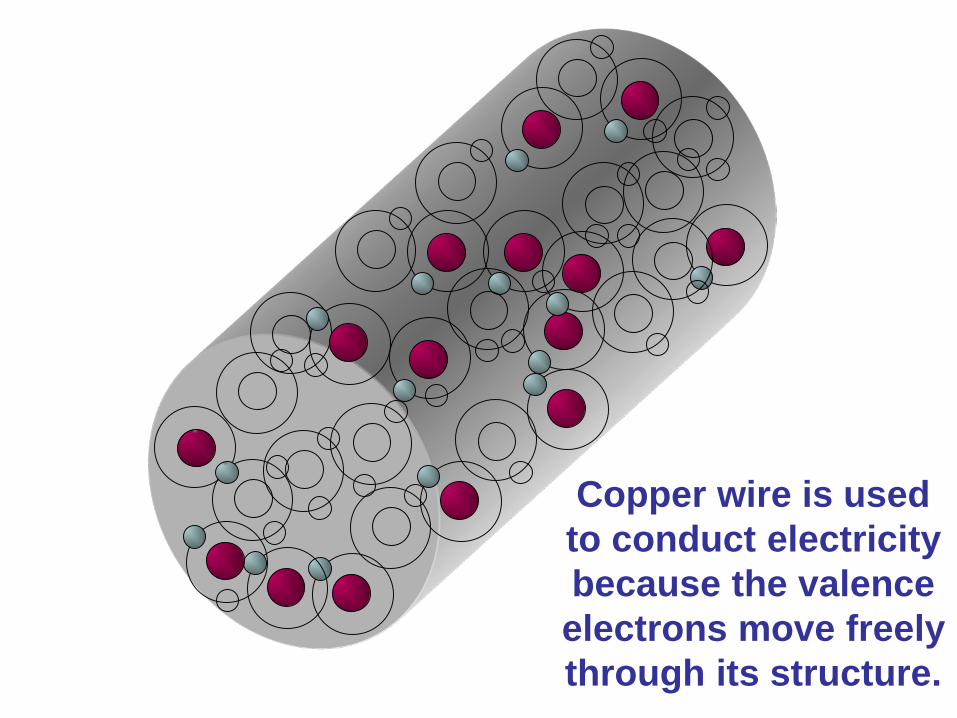
Copper wire is usedto conduct electricitybecause the valenceelectrons move freelythrough its structure.

So far, we know that copper’s single valence electron makes it a good conductor.
It acts as an electrical insulator.
The rule of eight states that a material like thiswould be stable since its valence orbit is full.
No Vacancy

31
Concept Review
• The nucleus of any atom is positively charged.• Negatively charged electrons orbit the nucleus.• The net charge on any atom is zero because the
protons and electrons are equal in number.• The valence orbit is the outermost orbit.• Copper has only one valence electron and is an
excellent conductor.• Materials with a full valence orbit act as
insulators.• Materials with 8 electrons in the valence orbit act
as insulators.
32
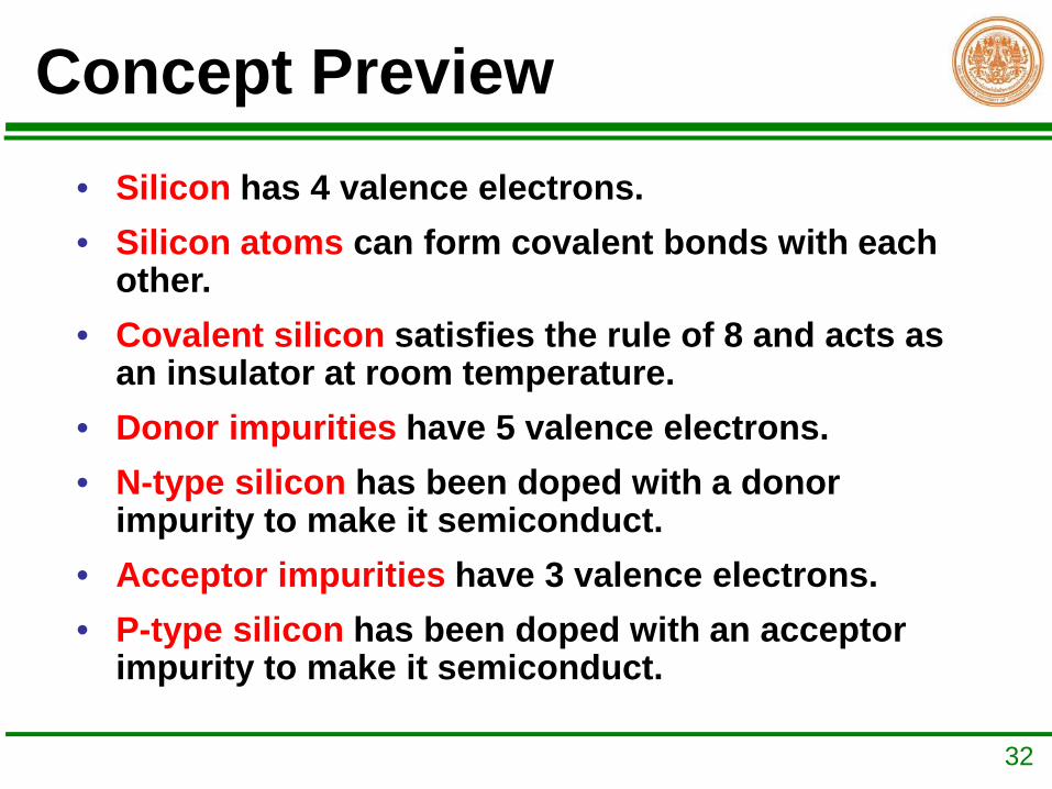
Concept Preview• Silicon has 4 valence electrons.• Silicon atoms can form covalent bonds with each
other.• Covalent silicon satisfies the rule of 8 and acts as
an insulator at room temperature.• Donor impurities have 5 valence electrons.• N-type silicon has been doped with a donor
impurity to make it semiconduct.• Acceptor impurities have 3 valence electrons.• P-type silicon has been doped with an acceptor
impurity to make it semiconduct.

33
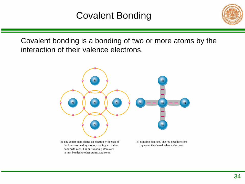
Atoms of the same type can join together and form covalent bonds.
This is an electron sharing process.
Silicon atoms have four valence electrons.
34
Covalent Bonding
Covalent bonding is a bonding of two or more atoms by the interaction of their valence electrons.
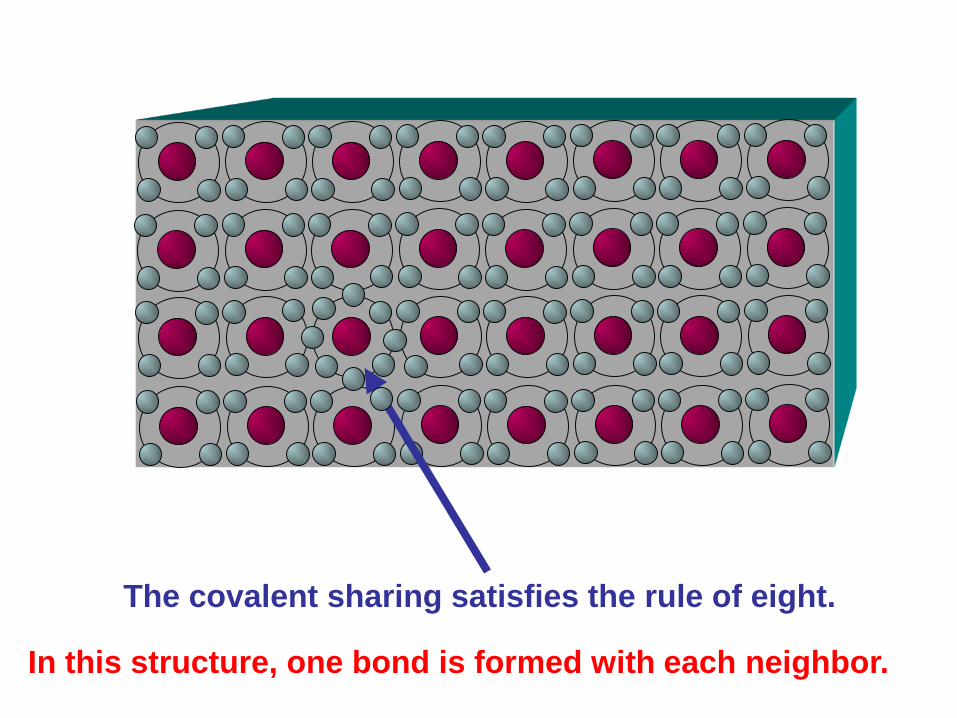
The covalent sharing satisfies the rule of eight.
In this structure, one bond is formed with each neighbor.

This is a silicon crystal.
It does not conduct because its valence electrons are captured by covalent bonds.

Thermal carriers
Covalent bonds can be broken by heating a silicon crystal.
Free electron
Hole
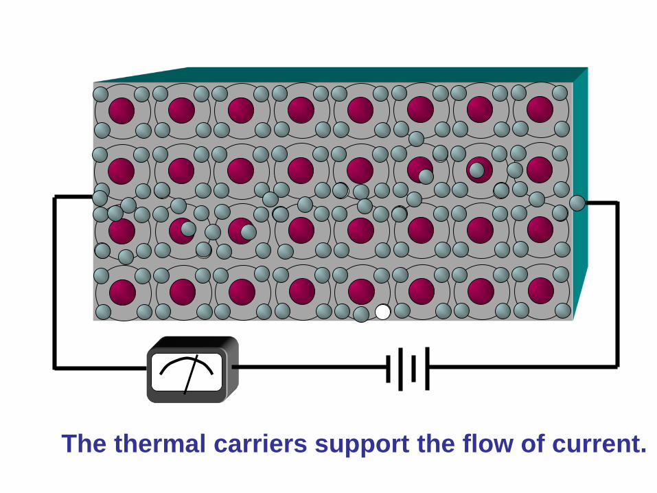
The thermal carriers support the flow of current.

Heating silicon crystals to make them conduct is not practical!

40
Silicon
• Silicon is used to create most semiconductors.• A pure semiconductor is often called an “intrinsic”
semiconductor. • The electronic properties and the conductivity of a
semiconductor can be changed in a controlled manner by adding very small quantities of other elements, called “dopants” to the intrinsic material.
• In semiconductor production, doping intentionally introduces impurities into an extremely pure (also referred to as intrinsic) semiconductor for the purpose of modulating its electrical properties.
41
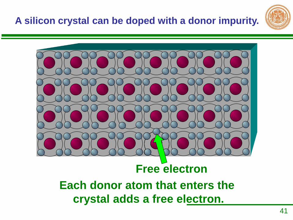
This is an arsenic atom.
A silicon crystal can be doped with a donor impurity.
1
2 3
45Free electron
Each donor atom that enters the crystal adds a free electron.

42
Silicon that has been doped with arsenic is called N-type.
The free electrons in N-type silicon support the flow of current.

43
This is a boron atom.
A silicon crystal can be doped with an acceptor impurity.
1
2 3
Each acceptor atom that enters the crystal creates a hole.
Hole
44
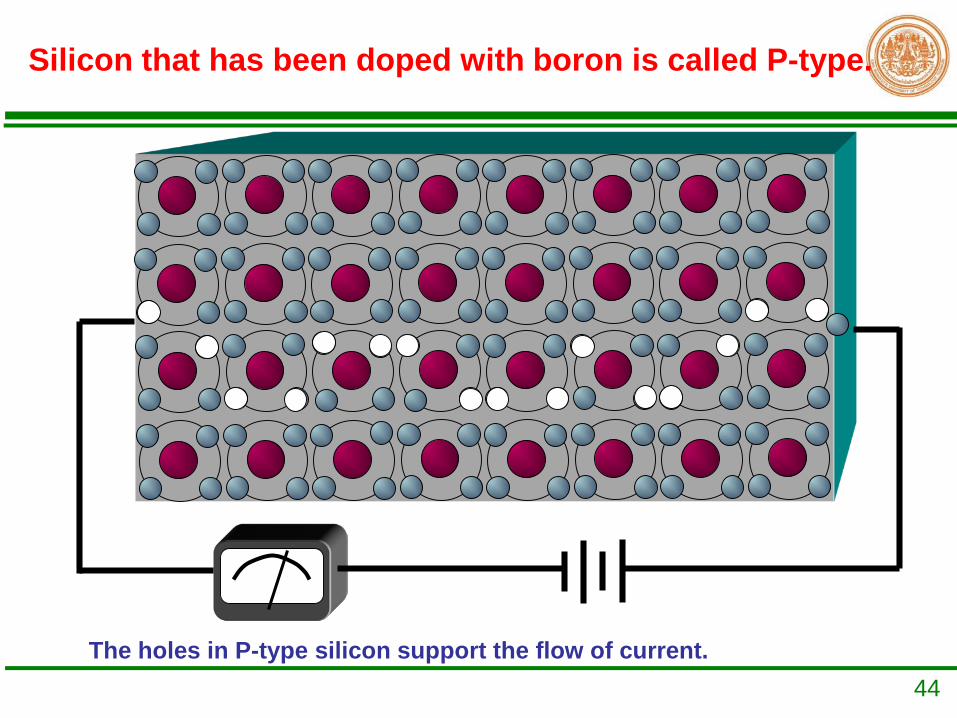
Silicon that has been doped with boron is called P-type.
The holes in P-type silicon support the flow of current.

45
What are two practical methodsof making silicon semiconduct?
HoleFree electron
Add a pentavalentimpurity.
Add a trivalentimpurity.
(N-type) (P-type)
N-P

46
N-type and P-type Semiconductors
Other atoms with 5 electrons such as Antimony(Sb) are added to Silicon to increase the free electrons.
Other atoms with 3 electrons such as Boron(B) are added to Silicon to create a deficiency of electrons or hole charges.
The process of creating N- and P-type materials is called doping.
N-type P-type
Boron(3e), arsenic(5e), phosphorus(5e), and gallium(3e) are normally used to dope silicon and germanium.

47
This is a P-type crystal.
Due to heat, it could have a few free electrons.These are called minority carriers.

48
This is an N-type crystal.
Due to heat, it could have a few free holes.These are called minority carriers.
49
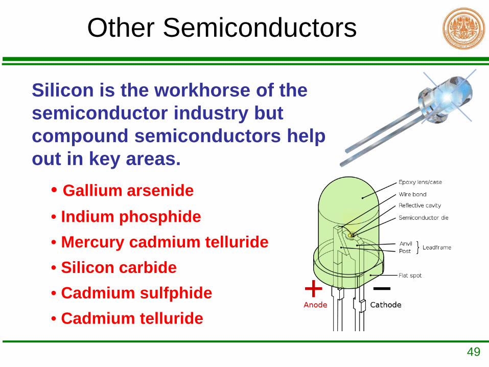
Other Semiconductors
Silicon is the workhorse of the semiconductor industry but compound semiconductors help out in key areas.
• Gallium arsenide• Indium phosphide• Mercury cadmium telluride• Silicon carbide• Cadmium sulfphide• Cadmium telluride