introduction of carbon nanotubes: properties, synthesis...
TRANSCRIPT

Chapter 1:
Introduction of Carbon Nanotubes: Properties,
Synthesis, Characterization and Applications
1.1. Background
1.2. Introduction of carbon and their
allotropes
1.3. Carbon nanotubes (CNTs)
1.4. Properties
1.5. Synthesis of CNTs
1.6. CNTs characterizations
1.7. Applications of CNTs
1.8. References


1
Chapter 1: Introduction of Carbon
Nanotubes: Properties, Synthesis,
Characterization and Applications
1.1. Background
In present scenario, human life is surrounded with different electronic
appliances and gadgets such as radio, television, computer, mobile, tab, etc. Although,
early age discovery of few of these equipments especially television and computing
systems were enabled with the invention of thermionic cathode and development of
vacuum electronics, however, it disappeared completely from these devices after
discovery of transistor in 1947 and later on integration of the basic circuit elements in
integrated semiconductor microelectronic devices. Basic circuit elements of
microelectronic devices are transistor, resistor and capacitor. These circuit elements
are versatile, cheap and robust compared to vacuum electronics. Integration of circuit
elements and invention of transistors enabled the miniaturization of electronic devices
such as computing system from room size ENIAC (electronic numerical integrator
and computer) in 1946 and EDVAC (electronic discrete variable automatic computer)
in 1951 to desktop computer in second-last decade of 20th century and laptop, palmtop
in 21st century. However, further scaling down of these devices is being studied to
enable some other revolutionary applications for its mass uses and user friendly
applications.
Great visionary Richard Feynman [1] lectured in a speech in 1959 that "there's
plenty of room in the bottom". This introduced and guided the basic research work in
atomic and molecular regime and given a platform to re-think about the nano
dimension devices. Few years later in 1965, Intel co-founder Moore predicted that
cramping and squeezing of more circuit components on single silicon chip will result
in reduction of their unit cost and miniaturization of computing systems. Moore's
prediction was the driving force for semiconductor industry and laid down the

Chapter 1: Introduction of Carbon Nanotubes: Properties, Synthesis, Characterization and Applications
2
foundation of new fabrication technology, process designing and their exciting
technological applications. This resulted in advancement of processing or fabrication
technology and miniaturization of electronic equipments. According to Moore's law,
the dimensions of individual devices in integrated microelectronic circuit decreases by
a factor of approximately two after every two years. This scaling down of devices has
driven the technological advancements in last few decades of 20th century and
resulted in development of different microprocessors, chips and many more.
Advancement in process technology and reduction of cost made computing devices
more accessible to people worldwide, and making the innovations and computing
more user friendly from the smallest handset to the largest cloud computing and
server.
Further scaling down of these devices has faced serious limitations. These
limitations are related to the fabrication technology, material parameters and device
performances as device dimension shrink down to a critical dimension below 22 nm
range. These limitations include lithography of substrate, short channel effects,
electron tunneling through short channels and thin insulator films, leakage currents,
passive power dissipation, variations in device structure, doping, etc. These
limitations can be overcome to some extent by modifying the channel material and
dielectric or insulating oxide of the conventional metal oxide semiconductor field
effect transistor (MOSFET) with some other nano material and high K-dielectric film.
Replacement of channel with single carbon nanotubes (CNTs) or an array of CNTs
[2] and insulator film by a high dielectric constant material such as hafnium oxide,
zirconium oxide, etc. are reported to facilitate/enable further scaling down of device
dimensions.
Moreover, there are certain applications where these solid state
microelectronic devices are impractical and the one and only one potential solution
for these applications is again the same vacuum electronics that was abandoned earlier
after invention of transistor. Although, thermionic cathodes possess certain major
disadvantages, such as high power consumption, bulky size, small life, etc. however,
other alternative of thermionic cathodes for these specialized applications is not yet
known. Few of these specialized applications such as microwave tubes for high-power
radio frequency transmission, certain military systems, X-ray machines, modern day

Chapter 1: Introduction of Carbon Nanotubes: Properties, Synthesis, Characterization and Applications
3
electron microscopy, etc. are still running with the same vacuum tube principle. These
systems use high speed of propagation of electron inside a high vacuum tube to
achieve desired operations. Similar to modern integrated semiconductor systems,
vacuum electronics based devices need to be integrated at micro-scale for its
successful applications.
With growing demand of device miniaturization, same as in the case of
integrated semiconductor technology, vacuum electronics also need to be miniaturized
for robust and compatible application with silicon technology in cathode ray tube,
field emission display, vacuum microelectronics, x-ray tube, etc. Nanomaterials,
nano-science and nanotechnology have attracted considerable attention due to their
comparable nanometer dimension and their great promise in device miniaturization.
The development of nanotechnology and nano-science was guided by revolutionary
lecture of Feynman and improvement of electron microscope resolution followed by
invention of scanning tunneling microscope in 1981. Later on during second last
decades of 20th century, nanotechnology research was further boosted with the
discovery of fullerenes in 1985 [3] and CNTs in 1991 [4]. Nano comes from a Greek
word ‘nanos’ which means dwarf. Nanotechnology is the study of functional and
advanced nano-material at the atomic and molecular scale that deals with a size range
between 1 to 100 nm or few nanometers to few micrometers.
Since the landmark paper by Iijima [4], CNTs have attracted remarkable
attention for different technological application. CNT is the fourth allotropes of
carbon and it has diameter in nanometers and length in micrometers. CNTs [5] are
reported to have numerous technological applications [6, 7] such as electron source
[8], field effect transistor (FET), sensor, composites [9], nano tips or probe etc. Tans
et al [2, 10] proposed that CNTs can replace the channel of MOSFET [7] for CNT
field effect transistor (CNTFET) application. The key advantages of CNTFET [6, 7]
are due to its high mobility, ballistic transport, high trans-conductance, high current
density, low threshold field, better control over channel formation, etc. However,
CNTFET fabrication technology and process compatibility with silicon [7] limit the
practical application of CNTFET. Major issues related to CNTFET [2] fabrication
includes positioning of CNTs at desired location, electrical contact formation between
CNTs and electrodes, mass production and repeatability in properties of CNTs. Other
Chapter 1: Introduction of Carbon Nanotubes: Properties, Synthesis, Characterization and Applications
4
promising application of CNTs may be as an electron emitter source [8, 11, 12] due to
its whisker geometry owing to their one dimensional structure. Utsumi [13, 14]
reported that whisker shape geometry exhibit highest field enhancement compared to
other structure. Many research groups have developed and demonstrated field
emission devices or electron field emitters using nano and micro-structured material
such as CNTs, silicon Spindt emitter [15-18], zinc oxide nano rod [19-21], nano-belts
[22], silicon carbide nano-wires [23, 24], aluminum nitride nano-needles [25, 26],
silicon nano-wires [18], tin oxide nano-whiskers [27] and more recently graphene
sheet [28, 29]. Among them, CNTs are considered to be relatively better electron
emitter source [14, 30] because of their unique physical, electrical, chemical and
mechanical properties [31].
CNT based field emitter arrays were reported to be developed using various
experimental methods [32-35] such as the suspension-filtering [36], screen printing
[37], electrophoresis, micro contact printing [38], spray [34], etc for different
applications. These experimental methods are post growth cathode development
approaches. In these methods, synthesized CNTs were mixed in different conducting
paste and mixture was transferred on the desired substrate. The major disadvantages
with these methods are poor adhesion [36] of CNTs with substrate, lack of vertical
alignment [39, 40], and no control on pattering [11] of CNTs in desired structure. In
addition to the above experimental methods, CNT field emitter arrays were also
reported to be prepared using a simple approach of direct chemical vapor deposition
(CVD) growth of CNTs on desired substrate. Direct CVD growth method resolves the
above issues of poor adhesion, patterning [11, 41] and vertical alignment of CNTs on
the substrate to some extent. However, CVD growth is carried out at elevated
temperature of more than 600oC and thus limits its wide application on different
substrate such as glass, indium tin oxide (ITO), etc. All these fabrication approaches
have some advantages and disadvantages, however direct CVD growth method is
preferred over the others and is used in my research work.
Title of my research work is "Study of Carbon Nanotubes Based Field
Emission Devices and their Characterization". During the research work, CNT
based electron emitter sources were developed using direct CVD growth and their
electron emission parameters were traded off using various techniques so that they

Chapter 1: Introduction of Carbon Nanotubes: Properties, Synthesis, Characterization and Applications
5
can exhibit enhanced emission properties. Entire work is organized in seven different
chapters of my thesis. The elaborative descriptions of each chapter are presented
below.
Chapter 1 is an introductory report on literature survey which gives brief
description of carbon with different allotropic forms. Different structural forms of
CNTs, their classification and their extraordinary properties have been reviewed and
discussed in different sections. Further, a review article has been presented on
different growth methods, growth mechanism, characterization techniques and
applications of CNTs.
Chapter 2 describes different electron emission mechanisms such as photo
electron emission, thermionic emission, secondary electron emission, field electron
emission and its background theory has been presented. Thermionic emission along
with the field-enhanced thermionic emission or Schottky emission is also elaborated.
Elaborative description of field emission and its analysis has been presented which is
essential to understand the experiment and its dependence on different parameters.
This is an introductory as well as analytical chapter which provides basic information
about the electron emission techniques and methods employed to derive and obtain
the field emission parameters which will be used in computing and analyzing the field
emission results in the later chapters. Field emission parameters include work
function, field enhancement factor, screening effect and effective emitting area.
Derivation of field emission parameters using quantum mechanical field emission
tunneling or Fowler-Nordheim equation have also been considered at the end.
Chapter 3 gives a detailed description of the experimental methodology
employed for the development of the CNTs based field emission devices.
Experimental methodologies employed to realize the CNTs based field emission
devices include CNT field emitter development, their characterization and FE
measurement in diode configuration. This chapter elaborates the process steps used
for development of CNTs based field emission devices i.e. CNTs based cathode or
CNT emitter arrays, which includes substrate cleaning, photolithography, catalyst
sputtering, lift off process and synthesis of CNTs using chemical vapor deposition or
plasma enhanced chemical vapor deposition. Different characterization tools such as
scanning electron microscope, transmission electron microscope, etc. employed to

Chapter 1: Introduction of Carbon Nanotubes: Properties, Synthesis, Characterization and Applications
6
study the morphology and the changes introduced after treatment has also been
elaborated. Finally, field emission study of the developed CNT emitter arrays has
been discussed at the end.
Field emission current density of the CNTs emitter arrays are reported to be
governed by Fowler-Nordheim (F-N) equation. F-N equation predicted that emission
current density is dependent on work function and enhanced electric field. The two
main experimental approaches that can be used to enhance the emission current of
existing cathode are reduction of effective work function and improvement of field
enhancement factor. Work function of a material is highly sensitive to the surface
properties, adsorbate and internal structure. Surface properties are reported to be
altered using surface modification approach by decorating them with low work
function materials. Conventional thermionic cathodes employ coating of low work
function material such as lanthanum hexaboride (LaB6), barium oxide etc. Similar
modification on the CNTs emitter surface, by coating them with different low work
function material, has been tried as an effective and simple approach to increase the
emission current of existing CNT cathodes.
Chapter 4 illustrates the different surface modification techniques employed
to alter the electron emission current of the existing CNT emitter arrays. In this
chapter, CNTs surfaces were modified with a different low work function material
such as lanthanum hexaboride (LaB6) and cesium iodide (CsI) and effect of surface
modification on their FE has been studied and analyzed. LaB6 is a traditional low
work function material and has well established industrial applications in filaments of
thermionic cathodes. In conventional thermionic cathodes, thick film of LaB6 is
coated on the tungsten filaments and their properties are well reported by different
authors. However in this chapter, LaB6 nano particles (NPs) were successfully
decorated on the patterned CNT emitter arrays and their effect was studied as
comparative change in FE. Subsequently, FE-results were analyzed in light of
effective change in work function due to LaB6 NPs decoration. Work function of
LaB6 NPs decorated CNTs was also estimated using mathematical reverse
engineering. Furthermore, cesium iodide nano particles decoration using thermal
evaporation and its influence on the emission current density of the CNT emitter

Chapter 1: Introduction of Carbon Nanotubes: Properties, Synthesis, Characterization and Applications
7
arrays has also been described. The possible reasons of this has been compared and
studied in light of Fowler Nordheim equation.
Chapter 5 reports effect of temperature treatment on FE of as-grown and low
work function decorated patterned CNT emitter arrays. Broken bonds, internal
structure stress and amorphous carbon deposited during growth of the CNTs have
been reported to be changed using thermal treatment. CNT emitter arrays were
temperature treated in different environment such as vacuum and air. To achieve the
enhanced emission current, as-grown CNTs were temperature treated in vacuum and
air at 1050°C and 400°C respectively. Furthermore, thermal treatment has been
tailored with the low work function decoration. Cesium iodide nano particles
decorated CNTs were vacuum annealed and oxidized CNTs were decorated with
LaB6 NPs.
Chapter 6 summarizes the effect of structural engineering on field emission
current of CNT emitter arrays. Structural engineering of CNT cathode in diode
structure involves the modification of CNT emitter arrays pattern. Owing to the high
aspect ratio, CNTs inherently keep the merit of very high field enhancement factor.
However, further trading in field enhancement factor is required for improved
emission current. The combined effect of the high aspect-ratio of CNTs and a low
work function material is expected to contribute towards the enhanced electric field
which along with relatively lower work function and this may result into a very high
current density. Different CNT emitter arrays were developed and its field emission
measurements were carried out to examine their effect on emission current density.
Present article intended to examine, analyze and illustrate the effect of edge length on
field emission of those different CNT emitter arrays that have minor difference in
edge length with major differences in graphitization and growth area.
Chapter 7 describes the conclusions and future plans of research work.
1.2. Introduction of carbon and their allotropes
Carbon has pre-historic discovery and is widely distributed in nature such as
sun, stars, comets, and atmospheres of most of the planets in different compounds and
various allotropic forms. In compound forms, carbon exists in different forms of

Chapter 1: Introduction of Carbon Nanotubes: Properties, Synthesis, Characterization and Applications
8
hydrocarbon, oxides, carbides, sulfides carbonates etc and their derivatives. Coal,
petroleum, and natural gas are chiefly occurring hydrocarbons. Moreover, carbon also
exists in some isotopic forms such as C12, C14 etc. In 1961 the International Union of
Pure and Applied chemistry adopted the C12-isotope as the basis of atomic weights
estimation and C14-isotope, with a half-life of 5715 years, were used for life time or
age estimation of materials such as wood, archaeological specimens, etc.
Carbon is sixth element of the periodic table. It is tetravalent in nature owing
to the four valence electrons in their outer most shell. It is unique among the elements
of periodic table because it has ability to form three different hybridization states such
as sp, sp2 and sp3 and can form single, double and triple bonds with carbon atom
itself and with other element too. Carbon forms a very large number of organic
compounds with hydrogen, oxygen, nitrogen, and other elements. There are close to
ten million known carbon compounds, many thousands of which are vital to organic
and life processes. Without carbon, the basis of life on earth would be impossible.
Figure 1.1 Illustration of sp3, sp2 and sp hybridization of carbon atom and its
bonding (source: http://mcat-review.org/bonding.php).
The property, due to which carbon atoms being linked to another carbon atom
by single, double and triple bond, is known as catenation property. Owing to the
catenation property, carbon atoms have an ability to form different allotropic forms.
Prior to the discovery of fullerene, CNTs and graphene, only three well-defined
allotropes of carbon were known which are diamond, graphite and amorphous carbon,
as depicted in Figure 1.2.

Chapter 1: Introduction of Carbon Nanotubes: Properties, Synthesis, Characterization and Applications
9
Figure 1.2 Allotropes of carbon: diamond, graphite and amorphous carbon.
Diamond is three-dimensional crystalline array of carbon atoms where carbon-
carbon atoms are linked by sp3 hybridization. The chemical bonds that hold the
carbon atoms in diamonds structure are three-dimensional (3D) network of lattice
atoms. Diamonds are also known to have different structural from and this is known
as hexagonal diamond or lonsdaleite which is presented in Figure 1.3. However,
graphite is a stacked sheet of two-dimensional (2D) network formed by hexagonal
arrays of carbon atoms where carbon-carbon atoms are linked together by sp2
hybridization. The atomic bonds formed in graphite lattice are covalently bonded
carbon-carbon atom and van der Waals force between the adjacent sheets. The weak
van der Waals force resulted to the easy sliding of the graphite sheets with respect to
each other and over each other, making it soft enough and so it is used in pencils to
form the streak marks and writing on the paper. Amorphous carbon is free and
reactive carbon that does not have any crystalline structure and possesses both sp3 as
well as sp2 hybridization states. This is also called diamond-like carbon. The physical
properties of carbon vary drastically with their allotropic form. The details of physical
properties changes in case of diamond and graphite due to change in allotropic form is
given in Table 1.1.

Chapter 1: Introduction of Carbon Nanotubes: Properties, Synthesis, Characterization and Applications
10
Table 1.1 Difference in physical properties of diamond and graphite owing to the
difference in structural forms and hybridization state
Diamond Graphite
Crystal structure : Cubic system Crystal structure: Hexagonal system
Clear and transparent Black and opaque
Hardest known material One of the softest material
Ultimate abrasive Soft and very good lubricant
Excellent electrical insulator Very good conductor of electricity
High thermal conductivity Thermal insulator
In 1985, Kroto, Curl, Smalley [3] and their group accidently synthesized third
form of carbon allotropes using laser vaporization technique of graphite rods in an
inert (helium) gas atmosphere. From the mass spectra of evaporated carbon
samples/soot, they observed a cage like molecular structure composed of 60 carbon
atoms joined together by single and double bonds to form a hollow spherical shape
with 12 pentagonal and 20 hexagonal faces. This resembles a highly symmetrical C60
sphere design of football, or soccer ball. The C60 molecule was named
buckminsterfullerene or, buckyball or fullerene after the American architect R.
Buckminster Fuller, as a respect of token, because geodesic dome structural principle
of Fuller were used for finding the structural stability of the 60 carbon atoms. In 1996,
this pioneering discovery and the trio scientist, Kroto, Curl, and Smalley, were
awarded with Nobel Prize. Same as diamond, fullerene also have different structural
forms such as C60, C70, C540 and these structural forms are given in Figure 1.3.
A fourth form of carbon allotrope was identified by Sumio Iijima of Japan in
1991 [4] and is known as CNTs. Therefore in 21st century, carbon has four different
known allotropic forms and further experiments and structural models were tested to
know the other possible forms of carbon. All of them have totally different physical
properties and posses very unique electrical, mechanical and thermal properties.
Similar to diamond and fullerene, CNTs are known to have different structural forms.

Chapter 1: Introduction of Carbon Nanotubes: Properties, Synthesis, Characterization and Applications
11
Figure 1.3 Typical representations of allotropes of carbon and its different structural
forms (a) diamond (b) lonsdaleite (hexagonal diamond) (c) graphite (d) fullerenes
(C60), (e) fullerenes (C540), (f) fullerenes (C70), (g) amorphous carbon and (h) single
walled CNTs (source: English Wikipedia, the free encyclopedia, 2013).
More recently, one atomic thick layer of graphite or the single two-
dimensional hexagonal arrays of carbon atoms, known as graphene, are attracting
remarkable attention due to their unique and extraordinary properties. Graphene is a
mono layer of sp2 bonded carbon atoms tightly packed in a two dimensional
honeycomb lattice. The carbon-carbon bond length in graphene is about 0.142 nm.
Graphene layers stacked together forms graphite with an inter-planar spacing of 0.335
nm. Each carbon atom is bonded in-plane together with σ bonds, providing a solid

Chapter 1: Introduction of Carbon Nanotubes: Properties, Synthesis, Characterization and Applications
12
hexagonal network while the out-of-plane π bonds accomplish the weak interaction
between different graphene layers. Bilayer and few layer graphene consist of 2 and 3
to 10 layers of these 2D sheets, respectively. Four basic allotropic forms of carbon are
presented in Figure 1.4.
Figure 1.4 Typical illustrations of the four basic allotropes of carbon: Diamond,
fullerene or buckminsterfullerene (C60), graphite or bilayer graphene, and CNTs.
The discovery of fullerene [3], CNTs and graphene has laid down the
foundation of a new branch of science known as nanotechnology nearly in the last
decade of the 20th century. The discovery of fullerenes greatly expanded research to
find out more number of different known allotropic forms of carbon, which until the
last decade of 20th century were limited to graphite, diamond, and amorphous carbon
such as soot and charcoal. Bucky-balls and bucky-tubes, also known as fullerene and
CNT due to their spherical and tubular structure, have been the subject of intense
research, both due to their unique chemistry and for their technological applications,
especially in materials science, electronics, and nanotechnology. These materials are
known as advanced material. The field of nanotechnology is divided into three major
categories according to the structural forms of carbon allotropes, (i) zero-dimensional
(0D) nanostructures such as quantum dots, fullerene (ii) one dimensional (1D)
Chapter 1: Introduction of Carbon Nanotubes: Properties, Synthesis, Characterization and Applications
13
nanostructures like nano-tubes, nano-wires, nano-rods and (iii) two-dimensional (2D)
structures example graphene, boron nitride, molybdenum sulfide and tungsten sulfide
nano sheets etc. Carbon emerges as one of the most remarkable elements found in a
significant number of compounds. Nanostructures of carbon are the most studied of
all other elements due to the ease in synthesizing these thermodynamically stable
carbon structures.
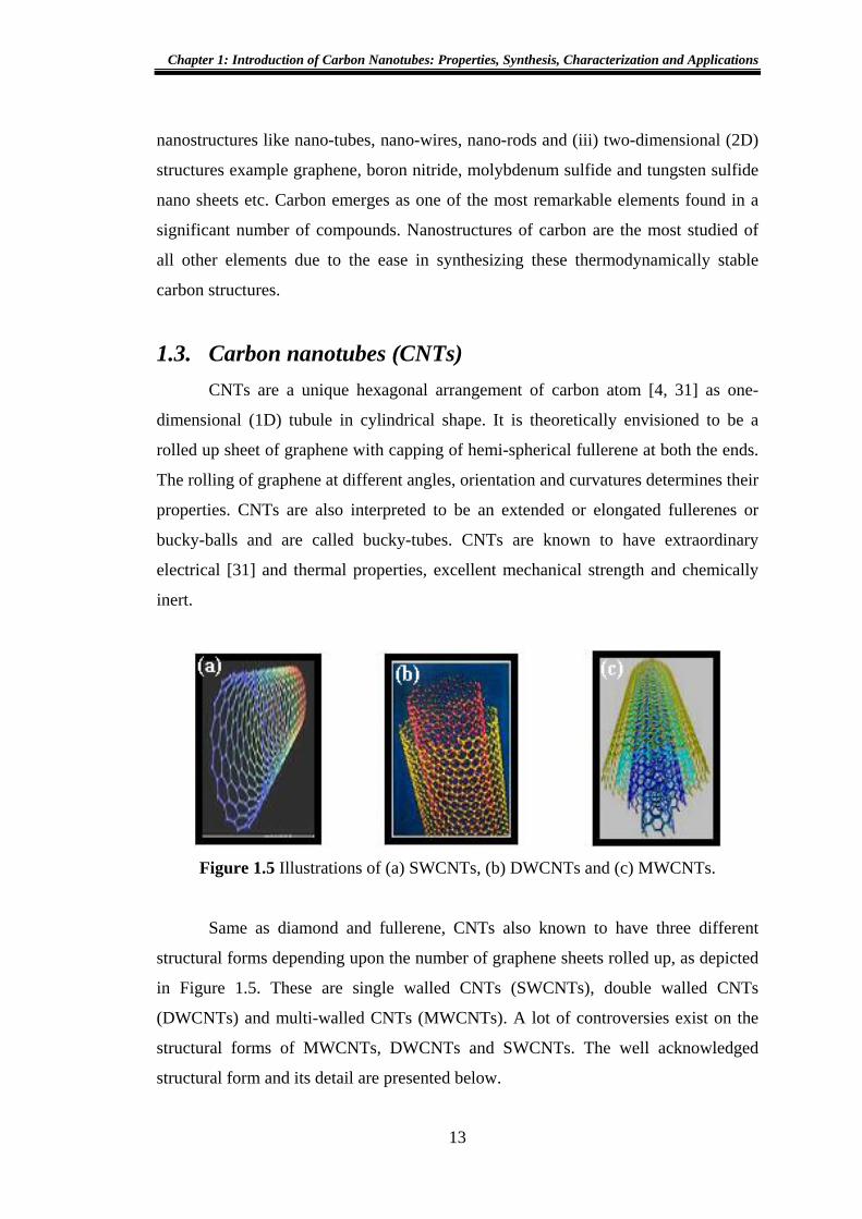
1.3. Carbon nanotubes (CNTs)
CNTs are a unique hexagonal arrangement of carbon atom [4, 31] as one-
dimensional (1D) tubule in cylindrical shape. It is theoretically envisioned to be a
rolled up sheet of graphene with capping of hemi-spherical fullerene at both the ends.
The rolling of graphene at different angles, orientation and curvatures determines their
properties. CNTs are also interpreted to be an extended or elongated fullerenes or
bucky-balls and are called bucky-tubes. CNTs are known to have extraordinary
electrical [31] and thermal properties, excellent mechanical strength and chemically
inert.
Figure 1.5 Illustrations of (a) SWCNTs, (b) DWCNTs and (c) MWCNTs.
Same as diamond and fullerene, CNTs also known to have three different
structural forms depending upon the number of graphene sheets rolled up, as depicted
in Figure 1.5. These are single walled CNTs (SWCNTs), double walled CNTs
(DWCNTs) and multi-walled CNTs (MWCNTs). A lot of controversies exist on the
structural forms of MWCNTs, DWCNTs and SWCNTs. The well acknowledged
structural form and its detail are presented below.

Chapter 1: Introduction of Carbon Nanotubes: Properties, Synthesis, Characterization and Applications
14
1.3.1. Single walled CNTs
Single walled CNTs (SWCNTs) structure was envisioned and conceptualized
to be a wrapping of one atomic thick layer of graphite, known as graphene, into a
seamless cylinder. Similar to the graphene sheet, SWCNTs are further classified [31]
into three types such as chiral SWCNTs, zigzag SWCNTs and armchair SWCNTs
according to different wrapping angle of the graphene sheet.
Figure 1.6 Typical illustration of graphene sheet [31]. This describes the chiral
vector, chiral angle, unit vectors and chiral index. Classification of graphene sheet:
armchair, zigzag and chiral according to different symmetry, chiral angle and chiral
vectors.
The wrapping of graphene sheet at different angle and orientations is
represented by a pair of indices (n, m), called chiral index and the angle with respect
to the chiral vector is known as chiral angle as depicted in Figure 1.6 and Table 1.2.
The integers n and m denote the number of unit vectors along two directions in the
honeycomb crystal lattice of carbon in the graphene sheet. If m = 0, the nanotubes are
called zigzag nanotubes, and if n = m, the nanotubes are called armchair nanotubes.
Otherwise, they are called chiral as shown in Figure 1.7 and Table 1.2. Chiral vector
of SWCNTs is represented through equation (1.1) and schematic of vector addition is
presented in Figure 1.6.

Chapter 1: Introduction of Carbon Nanotubes: Properties, Synthesis, Characterization and Applications
15
21 amanCh
rrr+= (1.1)
Where n & m are chiral indices and 1ar & 2a
r are real space unit vectors. The
rolling of graphene sheet at different angle and orientations with respect to the axial
direction of the cylinder, known as chiral axis determines its properties particularly
electrical and optical properties. Details of the electrical and optical properties are
discussed in section 1.4. Chiral angle of the zigzag SWCNTs, armchair SWCNTs and
chiral SWCNTs are mentioned in Table 1.2. The diameter of CNTs can be calculated
from its chiral indices (n, m) through the relation as follows.
mnnma
d ++=22
π (1.2)
For analysis of their electrical properties, the chiral vector of unrolled
honeycomb lattice of SWCNTs is defined theoretically along the twisting angle,
which is perpendicular to the axial direction of cylinder and is known as translational
vector.
Figure 1.7 Classification of SWCNTs according to chiral vector: Zigzag, chiral and
armchair CNTs [31].

Chapter 1: Introduction of Carbon Nanotubes: Properties, Synthesis, Characterization and Applications
16
Table 1.2 Classification of SWCNTs according to chiral index
CNT classification Chiral angle “θθθθ” [31] Chiral indices (n, m) [31]
Armchair SWCNTs 30° (n, m)
Zigzag SWCNTs 0° (n, 0)
Chiral SWCNTs 0° <θ<30° (n, m)
1.3.2. Double walled CNTs
In case of double-walled CNTs (DWCNTs) and multi-walled CNTs
(MWCNTs), more than one graphene sheets are rolled up into the concentric
cylindrical manner such that they have axial symmetry. Same as SWCNTs, DWCNT
are envisioned to have concentric wrapping of two hexagonal sheets of graphene into
seamless cylinder as shown in Figure 1.5(b).
1.3.3. Multi walled CNTs
Multi-walled CNTs (MWCNTs) are multiple concentric SWCNTs precisely
nested within one another. In other words, MWCNTs consist of multiple rolled up
layers of graphene in concentric tubules and its illustration is shown in Figure 1.5(c).
Different models were proposed to describe the structures of multi-walled nanotubes.
In general, sheets of graphite are envisioned to be arranged up in concentric cylinders
i.e. smaller SWCNTs lies within the larger SWCNTs. The interlayer distance in multi-
walled CNTs is close to the distance between graphene layers in graphite,
approximately 3.4 Å. Its individual shells can be described as SWCNTs, which can be
either metallic or semiconducting. Because of statistical probability and restrictions
on the relative diameters of the individual tubes, one of the shells and thus whole
MWCNTs usually behaves as a zero-gap metal.
1.4. Properties
Extensive experiments have been carried out to probe the electrical,
mechanical, chemical and thermal properties of CNTs. These studies suggested that
CNTs are reported to have extraordinary electrical properties, high mechanical
Chapter 1: Introduction of Carbon Nanotubes: Properties, Synthesis, Characterization and Applications
17
strength, excellent thermal conductivity and chemically inert nature. CNTs are
reported to have one dimensional structure as its length is in micrometer range and
diameter is of few nano meters. Same as fullerene is a zero dimensional material,
CNTs are known to be a one dimension material. The detail of each property will be
discussed in different subsections.
1.4.1.Electrical properties
From tight binding analysis [31], it had been seen that CNTs have both
metallic and semiconducting properties that depends upon their chiral index. The
electronic properties of CNTs are known to be extraordinary as it possess both
metallic as well as semiconducting behavior. Especially notable facts of the CNTs are
that they can be either metallic or semiconducting depending on their structure. Thus,
some nanotubes have conductivities higher than that of copper, while others behave
more like silicon. There is great interest in the possibility of constructing nano scale
electronic devices from CNTs, and some progress is already made in this area.
However, in order to construct a useful device, one requires to arrange many
thousands of CNTs in a defined pattern and needs full control, and we do not yet have
the degree of control necessary to achieve this. There are several areas of technology
where CNTs are already being used. These include flat-panel displays, scanning probe
microscopes and sensing devices. The unique properties of CNTs will undoubtedly
lead to many more applications.
Because of the symmetry and unique electronic structure of graphene, the
structure of a nanotube strongly affects its electrical properties. For a given (n, m)
CNTs, if n = m, the nanotube is metallic; if n - m is a multiple of 3, then the nanotube
is semiconducting with a very small band gap, otherwise the nanotube is a moderate
semiconductor. Thus all armchair (n = m) nanotubes are metallic, and (6, 4), (9, 1)
CNTs, etc. are semiconducting. Condition for metallic nanotube is that (2n + m) or
equivalently (n - m) is divisible by 3, otherwise the CNT shows semi conducting
behavior. However, this rule has exceptions, because curvature effects in small
diameter CNTs have strong influence on electrical properties. Thus, a (5, 0) SWCNTs
that should be semiconducting in fact is metallic according to the calculations.

Chapter 1: Introduction of Carbon Nanotubes: Properties, Synthesis, Characterization and Applications
18
Similarly, zigzag and chiral SWCNTs with small diameters that should be metallic
have finite gap and armchair nanotubes remain metallic always. In theory, metallic
nanotubes can carry an electric current density of 4 × 10⁹ A/cm2, which is more than
1,000 times greater than those of metals such as copper.
Figure 1.8 Metallic and semi-conducting CNTs [31] depending upon the chiral
indices (n, m).
Because of their quasi 1D structure or nanoscale cross-section, electrons
propagate only along the tube-axis and electron transport involves quantum effects.
As a result of this, CNTs are frequently referred to as one-dimensional conductors.
The maximum electrical conductance of a SWCNTs is 2G0, where G0 = 2e2/h is the
conductance of a single ballistic quantum channel.
1.4.2.Optical properties
Optical properties of CNTs [31] were observed due to electronic transitions
within one-dimensional density of states (DOS). A typical feature of one-dimensional
crystals is that their DOS is not a continuous function of energy, but it descends
gradually and then increases in a discontinuous spike [31]. In contrast, three-
dimensional materials have continuous DOS. The sharp peaks found in one-

Chapter 1: Introduction of Carbon Nanotubes: Properties, Synthesis,
dimensional materials are called
Optical properties of CNTs refer the Raman spectroscopy, emission and absorption
spectra with recent discovery in photoluminescence behavior.
of CNTs offers their quick and non destructive characterization.
Figure 1.9
SWCNTs (source: English Wikipedia, the free encyclopedia, 2013)
1.4.3.Mechanical p
The
mechanical properties. The stiffness of a material is measured in terms of its Young's
modulus, the rate of change of stress with respect to applied strain. The Young's
modulus of the best
approximately 5 times higher than steel. The tensile strength of nanotubes can be up
to 63GPa, around 50 times higher than steel. CNTs are the reported
the strongest and stiffest mater
elastic modulus
formed between the individual carbon atoms.
Chapter 1: Introduction of Carbon Nanotubes: Properties, Synthesis,
dimensional materials are called
Optical properties of CNTs refer the Raman spectroscopy, emission and absorption
spectra with recent discovery in photoluminescence behavior.
of CNTs offers their quick and non destructive characterization.
Density of states (DOS) of (a) metallic SWCNT
(source: English Wikipedia, the free encyclopedia, 2013)
Mechanical p
The high strength of sp2
mechanical properties. The stiffness of a material is measured in terms of its Young's
modulus, the rate of change of stress with respect to applied strain. The Young's
modulus of the best
pproximately 5 times higher than steel. The tensile strength of nanotubes can be up
GPa, around 50 times higher than steel. CNTs are the reported
the strongest and stiffest mater
elastic modulus respectively. This strength results from the covalent sp
formed between the individual carbon atoms.
Chapter 1: Introduction of Carbon Nanotubes: Properties, Synthesis,
dimensional materials are called
Optical properties of CNTs refer the Raman spectroscopy, emission and absorption
spectra with recent discovery in photoluminescence behavior.
of CNTs offers their quick and non destructive characterization.
Density of states (DOS) of (a) metallic SWCNT
(source: English Wikipedia, the free encyclopedia, 2013)
Mechanical properties
high strength of sp2
mechanical properties. The stiffness of a material is measured in terms of its Young's
modulus, the rate of change of stress with respect to applied strain. The Young's
modulus of the best nanotubes can be as high as 1
pproximately 5 times higher than steel. The tensile strength of nanotubes can be up
GPa, around 50 times higher than steel. CNTs are the reported
the strongest and stiffest materials yet discovered in terms of
respectively. This strength results from the covalent sp
formed between the individual carbon atoms.
Chapter 1: Introduction of Carbon Nanotubes: Properties, Synthesis,
19
dimensional materials are called Van Hove singularities as given in Figure 1.9
Optical properties of CNTs refer the Raman spectroscopy, emission and absorption
spectra with recent discovery in photoluminescence behavior.
of CNTs offers their quick and non destructive characterization.
Density of states (DOS) of (a) metallic SWCNT
(source: English Wikipedia, the free encyclopedia, 2013)
roperties
bonded carbon
mechanical properties. The stiffness of a material is measured in terms of its Young's
modulus, the rate of change of stress with respect to applied strain. The Young's
nanotubes can be as high as 1
pproximately 5 times higher than steel. The tensile strength of nanotubes can be up
GPa, around 50 times higher than steel. CNTs are the reported
ials yet discovered in terms of
respectively. This strength results from the covalent sp
formed between the individual carbon atoms.
Chapter 1: Introduction of Carbon Nanotubes: Properties, Synthesis,
Van Hove singularities as given in Figure 1.9
Optical properties of CNTs refer the Raman spectroscopy, emission and absorption
spectra with recent discovery in photoluminescence behavior.
of CNTs offers their quick and non destructive characterization.
Density of states (DOS) of (a) metallic SWCNT
(source: English Wikipedia, the free encyclopedia, 2013)
bonded carbon-carbon atoms gives CNTs amazing
mechanical properties. The stiffness of a material is measured in terms of its Young's
modulus, the rate of change of stress with respect to applied strain. The Young's
nanotubes can be as high as 1
pproximately 5 times higher than steel. The tensile strength of nanotubes can be up
GPa, around 50 times higher than steel. CNTs are the reported
ials yet discovered in terms of
respectively. This strength results from the covalent sp
formed between the individual carbon atoms. MWCNTs
Chapter 1: Introduction of Carbon Nanotubes: Properties, Synthesis, Characterization and Applications
Van Hove singularities as given in Figure 1.9
Optical properties of CNTs refer the Raman spectroscopy, emission and absorption
spectra with recent discovery in photoluminescence behavior. Optically act
of CNTs offers their quick and non destructive characterization.
Density of states (DOS) of (a) metallic SWCNTs and (b) semiconducting
(source: English Wikipedia, the free encyclopedia, 2013)
carbon atoms gives CNTs amazing
mechanical properties. The stiffness of a material is measured in terms of its Young's
modulus, the rate of change of stress with respect to applied strain. The Young's
nanotubes can be as high as 1000GPa
pproximately 5 times higher than steel. The tensile strength of nanotubes can be up
GPa, around 50 times higher than steel. CNTs are the reported
ials yet discovered in terms of tensile strength
respectively. This strength results from the covalent sp
WCNTs were reported to have
Characterization and Applications
Van Hove singularities as given in Figure 1.9
Optical properties of CNTs refer the Raman spectroscopy, emission and absorption
Optically active nature
(b) semiconducting
(source: English Wikipedia, the free encyclopedia, 2013).
carbon atoms gives CNTs amazing
mechanical properties. The stiffness of a material is measured in terms of its Young's
modulus, the rate of change of stress with respect to applied strain. The Young's
[42, 43] which is
pproximately 5 times higher than steel. The tensile strength of nanotubes can be up
GPa, around 50 times higher than steel. CNTs are the reported [44] to be
tensile strength
respectively. This strength results from the covalent sp2
reported to have
Characterization and Applications
Van Hove singularities as given in Figure 1.9.
Optical properties of CNTs refer the Raman spectroscopy, emission and absorption
ive nature
(b) semiconducting
carbon atoms gives CNTs amazing
mechanical properties. The stiffness of a material is measured in terms of its Young's
modulus, the rate of change of stress with respect to applied strain. The Young's
which is
pproximately 5 times higher than steel. The tensile strength of nanotubes can be up
to be one of
tensile strength and
2 bonds
reported to have tensile

Chapter 1: Introduction of Carbon Nanotubes: Properties, Synthesis, Characterization and Applications
20
strength of 63 GPa [42, 45]. Studies suggested that individual CNTs shells have
elastic strengths of 100 GPa [43]. Owing to the low density [46] and high strength, the
specific strength of CNT fibers [47] are much higher than the than the commercially
available fibers.
Although, it is well acknowledged [44] that the elastic strength of individual
CNT shells is extremely high, however, few reports [43] also suggested that weak
shear interactions between adjacent shells and tubes lead to the significant reductions
in the effective strength of MWCNTs and CNT bundles down to only a few GPa [43].
This has been recently addressed to improve the strength by applying high-energy
electron irradiation [43] in cross-linked hierarchical CNT bundles. They suggested
that cross linking of inner shells and tubes effectively attributed to increases the
strength of these materials to approximately 60GPa for MWCNT and 17GPa for
DWCNT bundles. Moreover, few papers also reported [44] that CNTs are not strong
enough to withstand high pressure under compressive load and buckling, kinking
were observed by them. They suggested that owing to their hollow structure and high
aspect ratio, CNTs tend to undergo buckling when placed under compressive load,
torsional strain and bending stress. SWCNTs can withstand a pressure up to 24GPa
without deformation. Furthermore, Popov et al [48] reported that bulk modulus of
super hard phase of SWCNTs is 462 to 546 GPa, which is higher than diamond
(single diamond crystal have 420 GPa).
1.4.4.Thermal properties
CNTs are reported [49] to have high thermal conductivity. It is a very good
thermal conductor along the tube axis and good insulators lateral to the tube axis. This
property is known as ballistic conduction. Pop et al [49] show that a SWCNTs has a
room temperature thermal conductivity of 3500 W·m−1·K−1 [49] along the tube axis.
This is much higher than the thermal conductivity of copper (385 W·m−1·K−1) which
is well known for its good thermal conductivity. They also reported that with increase
in room temperature, thermal conductivity decrease sharply and suggested that this
decrease is attributed to the phonon scattering. However, Sinha et al [50] reported that
Chapter 1: Introduction of Carbon Nanotubes: Properties, Synthesis, Characterization and Applications
21
SWCNTs film exhibit off-axis thermal conductivity of 1.64 W·m−1·K−1 at room
temperature.
1.4.5.Chemical properties
CNTs are reported to exhibit novel properties of chemical inertness. For some
specific application such as sensor and to make it selective to particular agent, CNTs
need to be functionalized with chemically selective species. Functionalization of
CNTs is well reported tough process and requires rigorous and aggressive acid
treatment at high temperature. Environmental particulates and gases generally
adsorbed on the walls of CNTs but it cannot react readily with this.
1.5. Synthesis of CNTs
The discovery of CNTs and their unique properties has led to an entirely new
understanding of the behavior of carbon materials, and it has opened a new chapter of
nano-science and nanotechnology as quoted in section 1.2 and the new chemistry of
complex systems at the atomic scale that exhibit advanced materials behavior.
Nanotubes in particular exhibit a wide range of novel mechanical and electronic
properties as discussed earlier in section 1.4. They are excellent conductors of heat
and electricity, and they possess an astonishing tensile strength. Such properties boost
the promise and exciting applications of CNTs in electronics, structural materials, and
medicine although few research suggest the toxic nature of CNTs. Practical
applications, however, will only be realized when accurate structural control has been
achieved over the synthesis of these new materials and to characterize them for a
particular application.
1.5.1.Catalyst deposition
Although there have been some studies reporting growth of CNTs without
catalyst in arc discharge process [4], it is widely acknowledged that transition metal
catalyst [51, 52] are needed for SWCNTs and MWCNTs growth. It is also believed
that the catalyst on the substrate must be in the form of particles instead of smooth,
continuous film. The metals which act as catalysts are basically transition [53] metals

Chapter 1: Introduction of Carbon Nanotubes: Properties, Synthesis, Characterization and Applications
22
like iron, nickel, cobalt and molybdenum. These metal catalysts can be applied on the
substrate from solutions containing them or they can be directly deposited using some
physical technique. The type of CNT required or their end use decides the choice of
approach. For example if we use solution form of catalyst, the powder form of CNTs
will be obtained while if we use the solid film of catalyst over the substrate, the CNTs
over the substrate can be obtained which is required for applications like field
emission display and electronic application. The powdered CNTs will be useful for
studying the purification and functionalization of CNTs.
Physical technique such as electron beam evaporation, thermal evaporation,
pulsed laser deposition, radio frequency (RF) sputtering, and magnetron sputtering
have been successfully used in catalyst preparation. These techniques are easy and
amenable to produce small patterns. Usually a thin catalyst film (less then 20nm) is
deposited by these techniques. The eventual particle size and the resultant nanotube
diameter seem to correlate to film thickness. Generally thinner film leads to smaller
particles and tube diameters but some optimization is always required, as only after a
particular thickness of the catalyst film the growth will take place. Although a small
grain size is not guaranteed in as prepared films. This depends on the growth
technique and the different pre treatment parameters used for breaking the films into
desired particle size. The catalyst film breaks into small islands due to surface tension,
as well as the compressive stress due to mismatch of the thermal expansion
coefficient of substrate and the catalyst film. In case of CVD, a pretreatment of
ammonia has been used where a catalyst film is simultaneously etched into small
particles.
1.5.2.Growth mechanism
Growth mechanism is the way in which CNTs are presumed to be formed
layer by layer. The growth mechanism of CNTs is not exactly known yet. It is still a
subject of controversy, and more than one growth mechanism has been proposed that
might be operative during the formation of CNTs. There are several theories on the
exact growth mechanism for nanotubes. One theory postulates that metal catalyst
particles are supported on the substrate as shown in Figure 1.10(a)-(b).

Chapter 1: Introduction of Carbon Nanotubes: Properties, Synthesis,
Figure 1.10
[54].
It presumes that the catalyst particles are spherical or pear
the deposition of nascent or reactive carbon will take place on only one half of the
surface and this is the lower curvature side for the pear shaped particles. The carbon
diffuses along the concentration gradient and precipitates on the opposite
and below the bisecting diameter. However, it does not precipitate from the apex of
the hemisphere, which accounts for the hollow core that is characteristic of these
filaments. For supported metals, filaments can form either by extrusion of C
upward and is also known as base growth, presented in Figure 1.10(a). CNTs grow
upwards from the metal particles and metal catalyst remain
or the particles detach and move at the head of the growing nanotube, labeled as tip
growth. Depending on the size of the catalyst particles, SWCNT
grown. In arc discharge, if no catalyst is present in the graphite, MWCNT
grown on the C
Chapter 1: Introduction of Carbon Nanotubes: Properties, Synthesis,
Figure 1.10 Illustrations of (a) tip growth mechanism and (b) base growth mechanism
It presumes that the catalyst particles are spherical or pear
the deposition of nascent or reactive carbon will take place on only one half of the
surface and this is the lower curvature side for the pear shaped particles. The carbon
diffuses along the concentration gradient and precipitates on the opposite
and below the bisecting diameter. However, it does not precipitate from the apex of
the hemisphere, which accounts for the hollow core that is characteristic of these
filaments. For supported metals, filaments can form either by extrusion of C
upward and is also known as base growth, presented in Figure 1.10(a). CNTs grow
upwards from the metal particles and metal catalyst remain
or the particles detach and move at the head of the growing nanotube, labeled as tip
growth. Depending on the size of the catalyst particles, SWCNT
grown. In arc discharge, if no catalyst is present in the graphite, MWCNT
grown on the C particles that are formed in the plasma.
Chapter 1: Introduction of Carbon Nanotubes: Properties, Synthesis,
Illustrations of (a) tip growth mechanism and (b) base growth mechanism
It presumes that the catalyst particles are spherical or pear
the deposition of nascent or reactive carbon will take place on only one half of the
surface and this is the lower curvature side for the pear shaped particles. The carbon
diffuses along the concentration gradient and precipitates on the opposite
and below the bisecting diameter. However, it does not precipitate from the apex of
the hemisphere, which accounts for the hollow core that is characteristic of these
filaments. For supported metals, filaments can form either by extrusion of C
upward and is also known as base growth, presented in Figure 1.10(a). CNTs grow
upwards from the metal particles and metal catalyst remain
or the particles detach and move at the head of the growing nanotube, labeled as tip
growth. Depending on the size of the catalyst particles, SWCNT
grown. In arc discharge, if no catalyst is present in the graphite, MWCNT
particles that are formed in the plasma.
Chapter 1: Introduction of Carbon Nanotubes: Properties, Synthesis,
23
Illustrations of (a) tip growth mechanism and (b) base growth mechanism
It presumes that the catalyst particles are spherical or pear
the deposition of nascent or reactive carbon will take place on only one half of the
surface and this is the lower curvature side for the pear shaped particles. The carbon
diffuses along the concentration gradient and precipitates on the opposite
and below the bisecting diameter. However, it does not precipitate from the apex of
the hemisphere, which accounts for the hollow core that is characteristic of these
filaments. For supported metals, filaments can form either by extrusion of C
upward and is also known as base growth, presented in Figure 1.10(a). CNTs grow
upwards from the metal particles and metal catalyst remain
or the particles detach and move at the head of the growing nanotube, labeled as tip
growth. Depending on the size of the catalyst particles, SWCNT
grown. In arc discharge, if no catalyst is present in the graphite, MWCNT
particles that are formed in the plasma.
Chapter 1: Introduction of Carbon Nanotubes: Properties, Synthesis,
Illustrations of (a) tip growth mechanism and (b) base growth mechanism
It presumes that the catalyst particles are spherical or pear
the deposition of nascent or reactive carbon will take place on only one half of the
surface and this is the lower curvature side for the pear shaped particles. The carbon
diffuses along the concentration gradient and precipitates on the opposite
and below the bisecting diameter. However, it does not precipitate from the apex of
the hemisphere, which accounts for the hollow core that is characteristic of these
filaments. For supported metals, filaments can form either by extrusion of C
upward and is also known as base growth, presented in Figure 1.10(a). CNTs grow
upwards from the metal particles and metal catalyst remain
or the particles detach and move at the head of the growing nanotube, labeled as tip
growth. Depending on the size of the catalyst particles, SWCNT
grown. In arc discharge, if no catalyst is present in the graphite, MWCNT
particles that are formed in the plasma.
Chapter 1: Introduction of Carbon Nanotubes: Properties, Synthesis, Characterization and Applications
Illustrations of (a) tip growth mechanism and (b) base growth mechanism
It presumes that the catalyst particles are spherical or pear-shaped. In t
the deposition of nascent or reactive carbon will take place on only one half of the
surface and this is the lower curvature side for the pear shaped particles. The carbon
diffuses along the concentration gradient and precipitates on the opposite
and below the bisecting diameter. However, it does not precipitate from the apex of
the hemisphere, which accounts for the hollow core that is characteristic of these
filaments. For supported metals, filaments can form either by extrusion of C
upward and is also known as base growth, presented in Figure 1.10(a). CNTs grow
upwards from the metal particles and metal catalyst remains attached to the substrate,
or the particles detach and move at the head of the growing nanotube, labeled as tip
growth. Depending on the size of the catalyst particles, SWCNTs
grown. In arc discharge, if no catalyst is present in the graphite, MWCNT
Characterization and Applications
Illustrations of (a) tip growth mechanism and (b) base growth mechanism
shaped. In t
the deposition of nascent or reactive carbon will take place on only one half of the
surface and this is the lower curvature side for the pear shaped particles. The carbon
diffuses along the concentration gradient and precipitates on the opposite half, around
and below the bisecting diameter. However, it does not precipitate from the apex of
the hemisphere, which accounts for the hollow core that is characteristic of these
filaments. For supported metals, filaments can form either by extrusion of C
upward and is also known as base growth, presented in Figure 1.10(a). CNTs grow
attached to the substrate,
or the particles detach and move at the head of the growing nanotube, labeled as tip
s or MWCNT
grown. In arc discharge, if no catalyst is present in the graphite, MWCNTs
Characterization and Applications
Illustrations of (a) tip growth mechanism and (b) base growth mechanism
shaped. In this case
the deposition of nascent or reactive carbon will take place on only one half of the
surface and this is the lower curvature side for the pear shaped particles. The carbon
half, around
and below the bisecting diameter. However, it does not precipitate from the apex of
the hemisphere, which accounts for the hollow core that is characteristic of these
filaments. For supported metals, filaments can form either by extrusion of CNTs
upward and is also known as base growth, presented in Figure 1.10(a). CNTs grow
attached to the substrate,
or the particles detach and move at the head of the growing nanotube, labeled as tip-
or MWCNTs are
s will be

Chapter 1: Introduction of Carbon Nanotubes: Properties, Synthesis, Characterization and Applications
24
1.5.3.Different growth techniques
Several growth techniques have been identified worldwide for synthesis of
CNT. Out of all these, here I am going to discuss mainly those three growth
techniques, which are in common uses.
1.5.3.1. Arc discharge method
Nearly two decades ago, Iijima at NEC fundamental research laboratory in
Tsukuba, Japan, first observed CNTs in the soot of carbon prepared by the carbon arc
discharge evaporation method [4] that was intended for the synthesis of C60 fullerene.
The schematic of arc discharge method is shown in Figure 1.11. Here cathode works
as the deposit electrode, which collects soot and the anode is a movable carbon rod,
which is consumed in the arc. The apparatus is attached to a vacuum pump and an
inert gas supply, usually helium (He) and argon (Ar). The carbon arc discharge
method used for synthesis of CNTs is simple and easy to operate however, to obtain
CNTs with high yields and purities; a careful control over the experimental conditions
is needed.
Figure 1.11 Schematic of arc discharge method.
DC Source
He gas at 500 Torr
Vacuum Pump
Graphite Cathode
Graphite Anode
Plasma
Deposited Soot
DC
Chapter 1: Introduction of Carbon Nanotubes: Properties, Synthesis, Characterization and Applications
25
Ar Gas
Furnace at 1200°C
Water Cooled Cu Collector
LASER Beam
Graphite Target
1.5.3.2. Laser ablation method
In 1995, T. Guo et al. [51] at Rice University first reported the laser ablation
technique for synthesis of single-walled nanotubes.
Figure 1.12 Schematic of laser ablation method.
In this method, a pulsed or continuous laser beam is applied to a carbon target
in order to vaporize the mixture of graphite and metal catalyst (Co, Ni). The main
difference between continuous and pulsed laser used is that the pulsed laser needs a
much higher light intensity i.e. 1000 kW/cm2 compared to 12 kW/cm2. The carbon
target is contained within a horizontal tube with the flow of inert gas, usually helium
and argon (Ar) at a pressure of 500 Torr. The whole assembly is kept inside an oven
at a temperature of 1200°C as shown in Figure 1.12. The CNTs are collected on a
water cooled copper (Cu) collector outside the furnace from evaporated graphite.
1.5.3.3. Chemical vapor deposition
Although the two methods mentioned above are the primary methods used for
the production of CNTs but they have few major disadvantages. First, both arc
discharge and laser ablation technique lack control on CNTs growth. Second, these
methods are relatively cost ineffective because growth temperature in arc discharge
and laser ablation methods are too high and therefore they consume huge amount of
energy. Third, CNTs grown through these methods have unwanted carbon and metal
impurities. However in chemical vapor deposition (CVD) synthesis method, excellent

Chapter 1: Introduction of Carbon Nanotubes: Properties, Synthesis, Characterization and Applications
26
alignment as well as position control at nanometer scale with control over the
diameter and deposition rate can be achieved at relatively low temperature.
For CVD growth technique, a thin patterned or continuous layer of metal
catalyst (Fe, Co, Ni or their alloy) is deposited on Si substrates, using thin film
deposition techniques like sputtering, e-beam and thermal evaporation. Energy supply
to the carbon containing source gases, which is injected inside the reactor through gas
line with MFC control, is done by resistively heated coil or ionized plasma. These
energy sources are used for cracking of gas molecule into reactive atomic carbon,
which precipitates at catalyst nano islands leading to the formation of CNTs.
Commonly used carbon feedstock gases include different hydrocarbons (CH4, C2H2,
C2H4, C2H6), carbon monoxide etc. CVD growth technique is further classified into
thermal CVD, plasma enhanced CVD, low pressure CVD, etc.
1.5.3.3.1. Thermal chemical vapor deposition
In thermal CVD method, catalyst deposited substrate were positioned on to the
sample holder. Sample holder then kept within the quartz tube of CVD reactor. Now,
sample is heated up to desired temperature using resistively heating coil. Pretreatment
was carried out at optimized temperature of 850°C or more for formation of catalytic
nano-island in the presence of ammonia (NH3) and hydrogen (H2) at atmospheric
pressure. Here, catalyst nano-island act as a nucleating seeds for growth of CNTs.
CNT growth was finally carried out at an elevated temperature range of 650°C-1200°C
using carbon feedstock gases in presence of NH3. Growth temperature depends up on
the choice of carbon feedstock gases used.
1.5.3.3.2. Plasma enhanced chemical vapor deposition
In the plasma-enhanced CVD, after positioning the sample on the grounded
electrode, a glow discharge of plasma is created using high frequency power supply at
a pressure of 10-1 mbar, inside the chamber that assists in pyrolytic dissociation of
carbon feedback gases into the nascent atomic carbon. In this process, plasma
enhances the process of dissociating the hydrocarbon into atomic carbon species and
therefore growth of CNTs in PECVD occurs at relatively lower temperature [39] than

Chapter 1: Introduction of Carbon Nanotubes: Properties, Synthesis, Characterization and Applications
27
thermal CVD. However, individual CNTs, which are grown by PECVD, contain more
defects in their sidewalls and are of poor quality because of the low growth
temperature.
1.6. CNTs characterization
CNTs are gaining remarkable attention on account of their potential and
diverse applications, which are attributed by virtue of their physical, electrical,
mechanical and thermal properties. For analysis of these properties, physical
morphology assessment and materialization of the proposed application, different
characterization techniques are employed. These characterization techniques include
electron microscope, atomic force microscope, Raman spectroscopy, thermo
gravimetric analysis, ultraviolet visible near infrared spectroscopy, scanning tunneling
microscope, Fourier transform infrared spectroscopy, etc. Diameter of CNTs is in few
nanometers and length is in micrometer, optical microscopes are inefficient tools for
morphological analysis of CNTs because its resolution seizes in this regime. Electron
microscope such as scanning electron microscopy (SEM) and tunneling electron
microscopy (TEM) [55] are two powerful instruments used for physical
characterization of nano-scale materials and CNTs. Detail of each characterization
techniques and their methodology employed to probe the properties has been
elaborated. Summary of different CNTs characterization techniques will be presented
in Table 1.3 with properties analysis.
1.6.1.Scanning electron microscope
Scanning electron microscope (SEM) is one of the most common tools used to
probe the morphological changes and quality of the synthesized CNTs. A SEM
instruments consisted of an electron gun, condenser lenses for electron beam
focusing, and vacuum system. SEM uses a beam of focused electrons in raster scan
aimed to analyze the specimen target. Focused electron beam moves in raster scan and
imaging is produced. SEM is mainly used to study the surface or near surface
structure of bulk specimens. The spatial resolution of SEM is approximately 15nm,
and therefore, not as good as TEM, which can have spatial resolutions in the sub-

Chapter 1: Introduction of Carbon Nanotubes: Properties, Synthesis, Characterization and Applications
28
nanometer range; however, SEM images are generally much easier to image and
interpret compared to TEM. Also SEM has the ability to image a comparatively large
area of the specimen; the ability to image bulk materials, thin films etc., and the
variety of analytical modes available for measuring the composition and nature of the
specimen.
Field emission SEM (FESEM) uses a field emission cathode as an electron
gun of a scanning electron microscope and provides narrow and fine probing beams
both at low and high electron energy; this results in both improved spatial resolution
and minimized sample charging and damage. FESEM produces clearer, less electro-
statically distorted images with spatial resolution down to 1.5nm or better i.e. several
times better than the conventional SEM. High quality, low voltage images are
obtained with negligible electrical charging of samples. Accelerating voltages of SEM
ranges from 0.5 to 30 kV.
Employing the SEM, surface morphology of as-grown CNTs as well as their
quality can be analyzed. From the SEM micrograph shown in chapter 3, one can
clearly see the vertical alignment and patterning of CNT bundles over the silicon
substrate. From high resolution SEM (HRSEM) images, amorphous carbon
contamination produced in the sample at the time of growth can also be analyzed.
Energy dispersive x-ray spectroscopy (EDX or EDS) can be used to study the
presence of metal catalyst or the grade of its removal achieved after the purification.
Chemical composition of the sample is analyzed using EDS. EDX analysis of CNTs
sample gives information about the quality of impurity.
1.6.2.Transmission electron microscope
Transmission electron microscopy (TEM) is one of the most common
techniques used to visualize and determine the morphology of the nano materials,
CNTs [56, 57] and nano-particles [57]. It is a very powerful electron microscope, used
for analysis of nano materials down to the angstrom level. Same as SEM, TEM
instruments have similar features such as an electron gun, condenser lenses, and a
vacuum system. However, TEM images production and magnification principle is
different from the SEM and thus TEM provides morphological information of the

Chapter 1: Introduction of Carbon Nanotubes: Properties, Synthesis, Characterization and Applications
29
nano-particles at higher magnification. In this technique, the specimen is illuminated
by a beam of monochromatic electrons; some of the electron beam are transmitted
through the objective lens and then projected onto a viewing screen. The viewing
screen composed of a layer of the electron fluorescent material to produce an image.
Figure 1.13 TEM micrograph of (a) MWCNTs, 6.7nm diameter and five concentric
graphene sheet, (b) DWCNTs, 5.5nm diameter and (c) MWCNTs, 6.5nm diameter
and seven tubular graphitic sheet [4].
In TEM micrograph one can see particles as small as a few angstroms 10-10 m,
which is near atomic levels. TEM is used to study the physical structure of CNTs i.e.
SWCNTs, DWCNTs [4] and MWCNTs and their dislocations. High-resolution
transmission electron microscopy (HRTEM) gives information about the number of

Chapter 1: Introduction of Carbon Nanotubes: Properties, Synthesis, Characterization and Applications
30
walls in MWCNT. HRTEM micrographs shown in Figure 1.13(a) and Figure 1.13(c)
shows MWCNTs with 6.7nm diameter having five concentric graphene sheet and
6.5nm diameter having seven tubular graphitic sheet whereas Figure 1.13(b) present
DWCNTs with 5.5nm diameter and two tubular concentric graphitic sheets.
1.6.3.Atomic force microscopy
Same as SEM and TEM, atomic force microscope (AFM) can also be used for
the analysis of surface morphology. SEM and TEM give 2D image, whereas AFM
images are three-dimensional. AFM is based on the raster scan of surface morphology
of sample using sharp tip of a cantilever probe. Imaging in AFM is done with the help
of monochromatic laser beam reflected from the back of cantilever. A typical AFM
image of CNTs is shown in Figure1.14.
Figure 1.14 AFM image of CNTs.
1.6.4.Raman spectroscopy
Raman spectroscopy is based on the Raman effect. Raman spectra of CNT are
rich in information about their structure and properties [31]. The spectrum also tells us
about the quality of the material, the structure of the tube, phonon and electron
quantum confinement. Raman spectroscopy is commonly used for characterizing
SWCNT bundles. Raman experiment can be done at room temperature and under
ambient pressure, so it is quick, non-destructive and does not require any sample

Chapter 1: Introduction of Carbon Nanotubes: Properties, Synthesis, Characterization and Applications
31
preparation experimentation. This technique has the sensitivity to probe differences in
the properties of CNTs prepared by different methods and under different conditions.
It also analyzes purity [58-60], the degree of amorphous carbon contained, and
impurities in the sample. Characterization of CNTs by Raman spectroscopy involves
following three dominant Raman bands that are the radial breathing mode (RBM) at
low frequencies, the tangential G band at higher frequencies and disorder-induced D-
band as shown in Figure 1.15.
The radial breathing mode (RBM) Raman frequencies corresponds to the
coherent vibration of the C atoms in the radial direction. These features are unique in
CNTs and occur with RBM frequencies between 120 cm−1 and 350 cm−1 for SWCNTs
with diameter range of 0.7 nm < d < 2 nm. These RBM frequencies are therefore very
useful for identifying whether a given carbon material contains SWCNTs, through the
presence of RBM mode and for characterizing the nanotube diameter distribution in
the sample.
Figure 1.15 Raman spectra of SWCNTs exhibit RBM peaks, defect peak, [60] silicon
peak and graphitic peak.
The G-band of CNT is related to the strain i.e. carbon-carbon stretching in
graphene plane. In SWCNT, G-band is composed of several peaks due to the phonon
wave vector confinement along the SWCNT circumferential direction and due to
symmetry-breaking effects associated with SWCNT curvature. The tangential G-band
appears in the range of 1500 cm-1 and 1605 cm-1. The D-band of CNTs is associated

Chapter 1: Introduction of Carbon Nanotubes: Properties, Synthesis, Characterization and Applications
32
with the disorder lying in the nanotube. The disorder-induced D-band that appears in
the range of 1300cm-1 and 1500cm-1 holds significant information about the
crystalline quality of the CNTs. The D-band comes into existence in the Raman-
spectrum only when sp2 hybridized carbon is lying adjacent to hetero-atoms, vacancy
defects, grain boundaries, or other defects that reduce the crystalline symmetry of
CNTs. Moreover, second over tone of defect peak, known as G’-band also appears
near 2700cm-1.
1.6.5.Thermo gravimetric analysis
Thermo-Gravimetric Analysis (TGA) is based on the thermal oxidation of the
CNT at elevated temperature treatment. Since, as grown CNTs have different
impurities like amorphous carbon and metal impurities viz. iron, cobalt, nickel or their
alloy. TGA is used to study the percentage of metal impurities lying in CNTs powder.
By thermal treatment of the CNT sample at high temperature, amorphous carbon
present in the sample burns at low temperature and CNT starts oxidizing. The
remaining ash of CNT powder, obtained after temperature treatment, is analyzed,
which gives information about the percentage of purity and thermal stability of CNT.
1.6.6.Ultraviolet visible near infrared
Ultraviolet visible near infrared (UV-Vis NIR) spectroscopy is a prominent
tool for analysis of local density of states (DOS) and conductivity of those compounds
which show electronic conjugation. CNTs show electronic conjugation due to the
delocalized π- electrons lying in hexagonal ring structure of their unit cell. Also, due
to the Quasi-1D structure of CNTs, electrons have one-dimensional confinement
along their axial direction. This gives rise to discredited DOS, which is known as van
Hove singularity. After exposure of CNTs sample in UV-Vis NIR radiation, electrons
lying in the valence band of the CNTs go into the excited un-occupied conduction
band. The emitted photons, when electron comes in to the valence band after de-
excitation, give S11 & S22 peaks for semi-conducting CNTs and M11 & M 22 peaks for
metallic CNTs in the UV-Vis NIR spectra. Using these peaks, one can estimate
electrical properties of CNTs i.e. metallic or semiconducting CNTs.

Chapter 1: Introduction of Carbon Nanotubes: Properties, Synthesis, Characterization and Applications
33
1.6.7.Scanning tunneling microscope
Scanning tunneling microscope (STM) works on the principle of quantum
tunneling of electron from the sample toward the nano-scale prober of the
microscope, after application of potential across the sample and probe tip. Since
quantum tunneling of electrons is directly related to the density of electronic states of
a system. Therefore through this instrument, one can study about the atomic structure
and electronic properties of CNT.
Table 1.3 Summary of CNTs characterization techniques
S. No. Characterization tools Properties Analyzed
1. Scanning electron microscope
(SEM)
Surface and physical morphology,
elemental analysis using EDX
2.
Transmission electron microscope
(TEM)
Defects, open cap, metal particle
encapsulation and 2D surface
morphology etc.
3. Atomic Force Microscopy
(AFM) 3-D surface morphology
4. Raman analysis Radius, defect, graphitization and
chiral index analysis etc.
5. Thermo Gravimetric analysis
(TGA) % ash and metal impurities content
6. Ultraviolet visible near infrared
spectroscopy (UV-Vis NIR)
Electrical properties analysis i.e.
metallic or semiconducting CNTs
7. Scanning tunneling microscope
(STM)
Atomic level imaging, chirality,
electrical properties
8. Fourier transform infra red
spectroscopy (FTIR)
Chemical analysis such as
functional group attachment etc.
1.6.8.Fourier transform infra red spectroscopy
This technique is based on the vibration spectra of CNTs. Fourier transform-
infrared (FTIR) spectroscopy is used to identify the chemical changes introduced due
Chapter 1: Introduction of Carbon Nanotubes: Properties, Synthesis, Characterization and Applications
34
to functional groups attachment with the CNTs samples. The FTIR sample is prepared
by grinding functionalized CNTs with KBr, and grinded CNT-KBr powder is made
into the form of pellets. These pellets are used for qualitative analysis of
functionalized CNTs. The FTIR peaks appear in the range of 1000cm-1 and 3500 cm-1
for different functionalized group.
1.7. Applications of CNTs
Since the landmark report of CNTs by Iijima in 1991 [4], CNTs and their
properties have been extensively studied and reported by various research groups.
These studies conclude that CNTs exhibited extraordinary electrical properties [31],
high mechanical strength, good thermal properties, high aspect ratio, and chemically
inert behavior. Owing to their unique properties of high aspect ratio, good mechanical
strength, chemical stability and semiconducting to metallic electrical behavior [61],
CNTs have been regarded as one of the most promising material for plethora of
applications ranging from biological [62], pharmaceutical, mechanical [63] to
electronics [6]. One of their major electronic applications is development of a CNT
based cathode for high and low current density devices such as vacuum
microelectronics, field emission (FE) displays, etc. For vacuum microelectronics
application, it is required to develop a CNT cathode possessing high electron emission
current because cathode is the basis and centre of a FE device.
CNTs have unique electrical properties such as the ability to with stand high
current density (109 A/cm2) low turn on electric field for cold electron emission and
show ballistic transport because of their quasi one-dimensional configuration. Due to
their unique properties, different research groups intensively study CNT’s behaviors
for device application. Apart from these, CNT have extraordinary mechanical and
chemical properties that make them potentially useful in many diverse applications
viz field emitter [64], sensor, energy storage, nano-composites etc. CNT can also be
used as nano interconnects due to their high current carrying capacity and ballistic
conductance, which arises due to their quasi-1D quantum confinement.
One of the most promising and interesting applications of CNT is in the field
of nano composites [9]. Nano composites are material matrix of more than one
compound that is in nano-meter scale such that they possess properties better than

Chapter 1: Introduction of Carbon Nanotubes: Properties, Synthesis, Characterization and Applications
35
each individual component. Due to the exceptionally high surface area to volume ratio
(typically in the range of 109 m-1) and high aspect ratio, high mechanical strength,
superior thermal conductivity, and unique electrical & optical properties, CNT can be
a very attractive reinforcing material and filler in material matrix of nano composite.
CNT can also be an excellent material for manufacturing of light weight armor and
aircraft. Another application of CNTs has been demonstrated as hydrogen storage.
Due to their high surface area, appreciable amount of hydrogen can be stored, per unit
weight of CNT. Apart for these applications, CNTs have also been identified as an
excellent candidate for many other applications such as memory, nano tweezers, nano
probe, solar applications, nano-genetic probe, nano electronics, AFM tip, etc.
Excellent mechanical strength coupled with the light weight of CNTs give its great
potential for aerospace, armoire applications. It has also been suggested that
nanotubes could be used in the space elevator, an Earth-to-space cable.
Figure 1.16 Proposed applications of CNTs.
1.7.1.Field emission and vacuum tube applications
The most promising application of CNTs are those involving electron field
emission [14, 30] devices and nano-electronics such as field effect transistors,

Chapter 1: Introduction of Carbon Nanotubes: Properties, Synthesis, Characterization and Applications
36
interconnects and sensors. Since, diameter of CNT are in few nanometers and length
is in microns, therefore it has high aspect ratio (Height/Radius), which makes them
excellent material for field induced electron emission at room temperature, also
known as cold cathode. CNT based cold cathode will be a very attractive electron
sources in a variety of applications, including field emission displays [65, 66], X-ray
tubes [67, 68], electron microscopy and vacuum microelectronics [69]. Numerous
efforts have been made for realization of CNT based vacuum devices, in which
vertically aligned, patterned CNTs are grown on substrate, which act as cathode.
These cathodes are tested in diode and triode configurations. A typical current
density-electric field (J-E) plot and F-N curves, obtained from current-voltage
characteristics has been presented in Figure 1.17. This confirms the field emission
behavior in diode structure and their suitability or applicability for vacuum
electronics.
Figure 1.17(a) J-E curves and (b) F-N Plots of CNT cathodes in diode configuration
at different anode to cathode spacing.
1.7.2.Sensors
CNTs have shown their potential candidature for sensor application due to
their high specific surface area and novel chemical inertness behavior. Due to some
major advantages in their physical, chemical and electrical behavior compared to
other material sensors, CNT based sensor will be relatively more sensitive and

Chapter 1: Introduction of Carbon Nanotubes: Properties, Synthesis, Characterization and Applications
37
efficient. Firstly, each atom of SWCNT is a surface atom, so, the sensitivity of CNT
based sensor is very high i.e. in ppt range. Second advantage is their ability to give
sufficient electrical response with change in environmental condition at room
temperature. This feature is very interesting for detection and realization of chemical
and gas sensors. Thirdly, foreign species are only physisorbed on the walls of CNT,
so re-utilization of CNT sensors will be possible after desorption of that foreign body.
Also CNTs can be made highly sensitive and selective to a particular species by
attaching its walls with a sensitive functional group, which works as receptors for that
species.
For realization of CNT based sensors many device approaches can be used
such as CNT resistor, capacitor, resonator, FET etc. Figure 1.18 shows a bottom gated
CNTFET for sensor application, where conductivity change in the channel of
CNTFET is analyzed for sensing of chemical and gas agents.
Figure 1.18 Bottom gated CNTFET for sensor application.
1.8. References
1. R. P. Feynman, There's plenty of room at the bottom. Microelectromechanical
Systems, Journal of, 1992. 1(1): p. 60-66.
2. Y. Feng, S. H. Huang, K. Kang, and Y.G Feng, Performances of carbon
nanotube field effect transistors with altered channel length. Science in China
Series E: Technological Sciences, 2010. 53(1): p. 253-256.

Chapter 1: Introduction of Carbon Nanotubes: Properties, Synthesis, Characterization and Applications
38
3. H. W. Kroto, J. R. Heath, S.C. O'Brien, R. F. Curl, and R. E. smalley, C60:
Buckminsterfullerene. Nature, 1985. 318(6042): p. 162-163.
4. S. Iijima, Helical microtubules of graphitic carbon. Nature, 1991. 354(6348):
p. 56-58.
5. Y. Ando, Carbon Nanotube: The Inside Story. Journal of Nanoscience and
Nanotechnology, 2010. 10(6): p. 3726-3738.
6. P. Avouris, Carbon nanotube electronics. Chemical Physics, 2002. 281(2-3):
p. 429-445.
7. P. Avouris, Molecular Electronics with Carbon Nanotubes. Accounts of
Chemical Research, 2002. 35(12): p. 1026-1034.
8. N. de Jonge, and J.-M. Bonard, Carbon nanotube electron sources and
applications. Philosophical Transactions of the Royal Society A:
Mathematical, Physical and Engineering Sciences, 2004. 362(1823): p. 2239-
2266.
9. E. T. Thostenson, Z. Ren, and T.-W. Chou, Advances in the science and
technology of carbon nanotubes and their composites: a review. Composites
Science and Technology, 2001. 61(13): p. 1899-1912.
10. S. J. Tans, A.R.M. Verschueren, and C. Dekker, Room-temperature transistor
based on a single carbon nanotube. Nature, 1998. 393(6680): p. 49-52.
11. C. Chien-Chao, T. Tsung-Yen, and T. Nyan-Hwa, Field emission properties of
carbon nanotube arrays through the pattern transfer process.
Nanotechnology, 2006(12): p. 2840.
12. K. Kunihiko, H Koichi, S. Hideki, and S. Yahachi, Development of
microfocused x-ray source by using carbon nanotube field emitter. Journal of
Vacuum Science and Technology B, 2006. 24(2): p. 950.
13. T. Utsumi, Vacuum microelectronics: what's new and exciting. Electron
Devices, IEEE Transactions on, 1991. 38(10): p. 2276-2283.

Chapter 1: Introduction of Carbon Nanotubes: Properties, Synthesis, Characterization and Applications
39
14. W. I. Milne, K.B.K. Teo, G. A. J. Amaratunga, P Legahneux, et al., Carbon
nanotubes as field emission sources. Journal of Materials Chemistry, 2004.
14(6): p. 933-943.
15. W. Xiaoju, L. Zulun, Q. Kangcheng, C. Zaxiang, et al., Field emission
characteristics of lanthanum hexaboride coated silicon field emitters. Journal
of Physics D: Applied Physics, 2007. 40(16): p. 4775.
16. S. J. Hong, S.J. Kwon, and E.S. Cho, Field emission properties of silicon field
emitter arrays with volcano-shaped gate structure. Current Applied Physics,
2009. 9(5): p. 967-971.
17. I. W. Rangelow, and S. Biehl, High aspect ratio silicon tips field emitter
array. Microelectronic Engineering, 2001. 57-58(0): p. 613-619.
18. E. C. Boswell, S. E. Huq, M Huang, P. D. Prewett, et al. Polycrystalline
silicon field emitters. in Vacuum Microelectronics Conference, 1995. IVMC.,
1995 International. 1995.
19. I. C. Yao, L. Pang, and T. Tseung-Yuen, Nanotip fabrication of zinc oxide
nanorods and their enhanced field emission properties. Nanotechnology,
2009. 20(12): p. 125202.
20. Z. Zhang, G. Meng, Q. Xu, Y Hu, et al., Aligned ZnO Nanorods with Tunable
Size and Field Emission on Native Si Substrate Achieved via Simple
Electrodeposition. The Journal of Physical Chemistry C, 2009. 114(1): p. 189-
193.
21. Y. Huang, and G. Yuan, Synthesis and field emission properties of ZnO
nanorods on Cu substrate. Materials Letters, 2012. 82(0): p. 85-87.
22. G. Z. Xing, X. S. Fang, Z. Zhang, D. D. Wang et al., Ultrathin single-crystal
ZnO nanobelts: Ag-catalyzed growth and field emission property.
Nanotechnology, 2010. 21(25): p. 255701.
23. W. M. Zhou, Y. J. Wu, E. S-W Kong, F. Zhu, et al., Field emission from
nonaligned SiC nanowires. Applied Surface Science, 2006. 253(4): p. 2056-
2058.

Chapter 1: Introduction of Carbon Nanotubes: Properties, Synthesis, Characterization and Applications
40
24. S. Z. Deng, Z. B. Li, W. L. Wang, N.S Xu, et al., Field emission study of SiC
nanowires/nanorods directly grown on SiC ceramic substrate. Applied
Physics Letters, 2006. 89(2): p. 023118-3.
25. Q. Zhao, J. Xu, X. Y Xu, Z Wang, et al., Field emission from AlN nanoneedle
arrays. Applied Physics Letters, 2004. 85(22): p. 5331-5333.
26. N. Liu, Q. Wu, C. He, H. Tao, et al., Patterned Growth and Field-Emission
Properties of AlN Nanocones. ACS Applied Materials & Interfaces, 2009.
1(9): p. 1927-1930.
27. S. H. Luo, Q. Wan, W. L. Liu, M. Zhang, et al., Vacuum electron field
emission from SnO2 nanowhiskers synthesized by thermal evaporation.
Nanotechnology, 2004. 15(11): p. 1424.
28. C.-K. Huang, Y. Ou, Y. Bie, Q. Zhao, et al., Well-aligned graphene arrays for
field emission displays. Applied Physics Letters, 2011. 98(26): p. 263104-3.
29. C. Wu, F. Li, Y. Zhang and T. Guo, Improving the field emission of graphene
by depositing zinc oxide nanorods on its surface. Carbon, 2012. 50(10): p.
3622-3626.
30. W. Zhu, C. Bower, O. Zhou, G. Kocjanski, et al., Large current density from
carbon nanotube field emitters. Applied Physics Letters, 1999. 75(6): p. 873-
875.
31. R. Saito, G. Dresselhaus, and M.S. Dresselhaus, Physical Properties of
Carbon Nanotubes. Imperial College Press, 1998
32. S. Xuefeng, G. Jingyun, F. Qiang, X. Jun, et al., Novel planar field emission of
ultra-thin individual carbon nanotubes. Nanotechnology, 2009. 20(40): p.
405208.
33. H. J. Jeong, S. C. Lim, K. S. Kim, and Y. H. Lee, Edge effect on the field
emission properties from vertically aligned carbon nanotube arrays. Carbon,
2004. 42(14): p. 3036-3039.

Chapter 1: Introduction of Carbon Nanotubes: Properties, Synthesis, Characterization and Applications
41
34. H. J. Jeong, H. K. Choi, G. Y. Kim, Y II Song, et al., Fabrication of efficient
field emitters with thin multiwalled carbon nanotubes using spray method.
Carbon, 2006. 44(13): p. 2689-2693.
35. J. H. Park, J.H. Choi, J-S Moon, D. G. Kushinov, et al., Simple approach for
the fabrication of carbon nanotube field emitter using conducting paste.
Carbon, 2005. 43(4): p. 698-703.
36. C. Ju Sung, L. Han Sung, J. Goak, E. Agustina, et al. High current carbon
nanotube field emitters fabricated by filtration and oxide layer coating. in
Vacuum Nanoelectronics Conference (IVNC), 2012 25th International. 2012.
37. Y. S. Shi, C-C Zhu, W. Qikun, and L. Xin, Large area screen-printing
cathode of CNT for FED. Diamond and Related Materials, 2003. 12(9): p.
1449-1452.
38. L. Nilsson, O Groening, C. Emmenegger, O. Kuettel, et al., Scanning field
emission from patterned carbon nanotube films. Applied Physics Letters,
2000. 76(15): p. 2071-2073.
39. M. Chhowalla, K. B. K. Teo, C. Ducati, N. L. Rupesinghe, et al., Growth
process conditions of vertically aligned carbon nanotubes using plasma
enhanced chemical vapor deposition. Journal of Applied Physics, 2001.
90(10): p. 5308-5317.
40. S. Saengmee-anupharb, S. Thongpang, E. S. P. Bertheir, and P. Singiai,
Growth of Vertically Aligned Carbon Nanotubes on Silicon Using a Sparked
Iron-Cobalt Catalyst. ISRN Nanotechnology, 2011. 2011: p. 8.
41. P. Chaturvedi, S. Pal, S. Lamba, A. B. Dhaulakhandi, et al., Selective growth
of multiwalled carbon nanotubes using chemical vapour deposition. Proc. of
IWPSD-2003: p. 974-978.
42. B. G. Demczyk, Y. M. Wang, J. Cumings, M. Hetman, et al., Direct
mechanical measurement of the tensile strength and elastic modulus of
multiwalled carbon nanotubes. Materials Science and Engineering: A, 2002.
334(1-2): p. 173-178.

Chapter 1: Introduction of Carbon Nanotubes: Properties, Synthesis, Characterization and Applications
42
43. T. Filleter, R. Bernal, S. Li, and H. D. Espinosa, Ultrahigh Strength and
Stiffness in Cross-Linked Hierarchical Carbon Nanotube Bundles. Advanced
Materials, 2011. 23(25): p. 2855-2860.
44. K. Jensen, W. Mickelson, A. Kis, and A. Zettl, Buckling and kinking force
measurements on individual multiwalled carbon nanotubes. Physical Review
B, 2007. 76(19): p. 195436.
45. M.-F. Yu, O. Lourie, M. J. Dyer, K. Moloni, et al., Strength and Breaking
Mechanism of Multiwalled Carbon Nanotubes Under Tensile Load. Science,
2000. 287(5453): p. 637-640.
46. J. H. Lehman, M. Terrones, E. Mansfield, K. E. Hurst, et al., Evaluating the
characteristics of multiwall carbon nanotubes. Carbon, 2011. 49(8): p. 2581-
2602.
47. X. Zhang, Q. Li, T. G. Holesinger, P. N. Arendt, et al., Ultrastrong, Stiff, and
Lightweight Carbon-Nanotube Fibers. Advanced Materials, 2007. 19(23): p.
4198-4201.
48. M. Popov, M. Kyotani, R. J. Nemanich, and Y. Koga, Superhard phase
composed of single-wall carbon nanotubes. Physical Review B, 2002. 65(3):
p. 033408.
49. E. Pop, D. Mann, Q. Wang, K. Goodson, et al., Thermal Conductance of an
Individual Single-Wall Carbon Nanotube above Room Temperature. Nano
Letters, 2005. 6(1): p. 96-100.
50. S. Sinha, S. Barjami, G. Lannacchione, A. Schwab, et al., Off-axis Thermal
Properties of Carbon Nanotube Films. Journal of Nanoparticle Research,
2005. 7(6): p. 651-657.
51. T. Guo, P. Nikolaev, A. Thess, D. T. Colbert, et al., Catalytic growth of
single-walled manotubes by laser vaporization. Chemical Physics Letters,
1995. 243(1-2): p. 49-54.
52. N. Sayangdev, and K.P. Ishwar, A model for catalytic growth of carbon
nanotubes. Journal of Physics D: Applied Physics, 2008. 41(6): p. 065304.

Chapter 1: Introduction of Carbon Nanotubes: Properties, Synthesis, Characterization and Applications
43
53. P. Chaturvedi, P. Verma, A. Singh, P.K. Chaudhary, et al., Carbon Nanotube-
Purification and Sorting Protocols. Defence Science Journal, 2008. 58(5).
54 M. Kumar, and Y. Ando, Chemical Vapor Deposition of Carbon Nanotubes: A
Review on Growth Mechanism and Mass Production. Journal of Nanoscience
and Nanotechnology, 2010. 10(6): p. 3739-3758.
55. D. Maya, K. Monja, and J. Niels de, In situ transmission electron microscopy
investigation of the structural changes in carbon nanotubes during electron
emission at high currents. Nanotechnology, 2006. 17(13): p. 3226.
56. M Kumari, S. Gautam, P. V. Shah, S. Pal, et al., Improving the field emission
of carbon nanotubes by lanthanum-hexaboride nano-particles decoration.
Applied Physics Letters, 2012. 101(12): p. 123116.
57. M. Shahi, S. Gautam, P. V. Shah, J. S. Rawat, et al., Decoration of cesium
iodide nano particles on patterned carbon nanotube emitter arrays to improve
their field emission. Journal of Nanoparticle Research, 2013. 15(3): p. 1497(1-
9).
58. R. A. DiLeo, B.J. Landi, and R.P. Raffaelle, Purity assessment of multiwalled
carbon nanotubes by Raman spectroscopy. Journal of Applied Physics, 2007.
101(6): p. 064307-5.
59. W. S. Kim, H. Oki, A. Kinoshita, K. Murakami, et al., Relationship between
field-emission characteristics and defects measured by Raman scattering in
carbon-nanotube cathodes treated by plasma and laser. Journal of Vacuum
Science and Technology B, 2008. 26(2): p. 760.
60. M.S. Dresselhaus, G. Dresselhaus, R. Saito, and A Jorio, Raman spectroscopy
of carbon nanotubes. Physics Reports, 2005. 409(2): p. 47-99.
61. C. Jean-Christophe, B. Xavier, and R. Stephan, Electronic and transport
properties of nanotubes. Reviews of Modern Physics, 2007. 79(2): p. 677.
62. W. Yang, P. Thordarson, J J. Gooding, S. P. Ringer, et al., Carbon nanotubes
for biological and biomedical applications. Nanotechnology, 2007. 18(41): p.
412001.

Chapter 1: Introduction of Carbon Nanotubes: Properties, Synthesis, Characterization and Applications
44
63. M Endo, M. S. Strano, and P. M. Ajayan, Potential Applications of Carbon
Nanotubes. Carbon Nanotubes, 2008. 111: p. 13-61.
64. J.-M. Bonard, M. Croci, C. Klinke, R. Kurt, et al., Carbon nanotube films as
electron field emitters. Carbon, 2002. 40(10): p. 1715-1728.
65. A. A. Kuznetzov, S.B. Lee, M. Zhang, R. H. Baughman, et al., Electron field
emission from transparent multiwalled carbon nanotube sheets for inverted
field emission displays. Carbon, 2010. 48(1): p. 41-46.
66. P. Chaturvedi, S. Pal, A. K. Puri, S. Lamba, et al., Carbon Nanotubes Based
Field Emission Displays. Proc. ICON-2003, 2003: p. 371-377.
67. J. Jin-Woo, K. Jae-Woo, K. Jun-Tae, C. Sungyoul, et al., A vacuum-sealed
compact x-ray tube based on focused carbon nanotube field-emission
electrons. Nanotechnology, 2013. 24(8): p. 085201.
68. H. Sugie, M. Tanemura, V. Filip, K. Iwata, et al., Carbon nanotubes as
electron source in an x-ray tube. Applied Physics Letters, 2001. 78(17): p.
2578-2580.
69. K. B. K. Teo, E. Minoux, L. Hudanski, F. Peauger, et al., Microwave devices:
Carbon nanotubes as cold cathodes. Nature, 2005. 437(7061): p. 968-968.