interface and traps in pentacene organic field-effect transistor
TRANSCRIPT
8/7/2019 Interface and Traps in Pentacene Organic Field-effect Transistor
http://slidepdf.com/reader/full/interface-and-traps-in-pentacene-organic-field-effect-transistor 1/7
Interfaces and traps in pentacene eld-effect transistorC. S. Suchand Sangeeth, 1,a P. Stadler, 2 S. Schaur, 2 N. S. Sariciftci, 2 and Reghu Menon 11 Department of Physics, Indian Institute of Science, Bangalore 560012, India2 Linz Institute for Organic Solar Cells (LIOS) and Institute for Physical Chemistry, Johannes Kepler University, Altenberger Strasse 69, 4040 Linz, Austria
Received 16 August 2010; accepted 18 October 2010; published online 2 December 2010The equivalent circuit parameters for a pentacene organic eld-effect transistor are determined fromlow frequency impedance measurements in the dark as well as under light illumination. Thesource-drain channel impedance parameters are obtained from Bode plot analysis and the deviationsat low frequency are mainly due to the contact impedance. The charge accumulation at organicsemiconductor–metal interface and dielectric–semiconductor interface is monitored from theresponse to light as an additional parameter to nd out the contributions arising from photovoltaicand photoconductive effects. The shift in threshold voltage is due to the accumulation of photogenerated carriers under source-drain electrodes and at dielectric–semiconductor interface, andalso this dominates the carrier transport. The charge carrier trapping at various interfaces and in thesemiconductor is estimated from the dc and ac impedance measurements under illumination.© 2010 American Institute of Physics . doi:10.1063/1.3517085
I. INTRODUCTION
Considerable interest in organic eld-effect transistorsOFETs based on small molecules, polymers and compos-
ites have emerged in past few years due to the low costof fabrication, ease of processing and mechanical exibility.1–3
Organic semiconductors can be processed from solution atroom temperature and printed onto a variety of exible sub-strates. Although the device performance of OFETs is typi-cally lower than that of inorganic counterparts, printed elec-tronic circuits using OFETs may become viable alternative tosilicon based systems, especially in large-area applications.4,5
Pentacene, a member of the oligoacene family, standsout as an attractive candidate for OFET applications on ac-count of its relatively high charge carrier mobility of theorder of 1 cm2/ V s.6 The electrical characteristics of the de-vices are dominated by the interface between pentacene andgate dielectric, and also the interfaces with source and drainmetal contacts. Various phenomena like energy level align-ment, dipole layer formation and band bending in the organiclayers occur at the interfaces that often create injection bar-riers, relevant for the FET operation. In the source-drainSD electrodes–semiconductor interface, contact resistance
affects the carrier injection and low barrier height ispreferred.7 As the device dimension decreases, the contactresistance as a part of the total device resistance will domi-
nate over the channel resistance, and thereby limiting thetransport in OFETs which determine the speed of organicintegrated circuits, then the role of intrinsic carrier mobilityof organic semiconductor becomes less dominant.8 The de-pendence of contact resistance in top-contactTC andbottom-contactBC geometrical congurations of pentaceneOFET shows that TC-OFETs of fers lower resistance becauseof the increased area of contact.9 The TC-OFETs have supe-rior performance and ease of fabrication but lacks suitable
procedure to patternthe FET active layer to isolate the devices from each other.10 In BC-OFETs, drain and source contact metal is deposited on the gate dielectric and patternprior to the active layer deposition. In this geometry tsource and drain series resistance are nonlinear, especiallyaffecting the transport at lowV DS.10,11 Hence optimization of the interface between SD electrodes and organic semicoductor along with the gate dielectric–semiconductor interfare the important factors to enhance the OFET performanSoft contact lamination of SD electrodes by gold-coahigh-resolution rubber stamps on the organic semiconduclms showed improved performance as the mechanical cformability is enhanced and the chemical modications alowered.12 Further, doping the semiconductor at source dracontactinterfaces has reduced the contact resistance to somextend.13 However, a detailed characterization of the intefaces are yet to be carried out to improve the overall perfmance of OFETs.
The performance of OFETs depends crucially on the uof dielectrics which form active interfaces with the orgasemiconductor. The ON or OFF states of an OFET is detmined by the presence or absence of gate-induced chargethe semiconductor–dielectric interface.14 The structural andelectrostatic disorder in the rst few layers of the organsemiconductor next to the insulator cause undesirable effelike lowering the OFET ON current, reduction in the swit
ing speed, hysteresis, and increase in the thresholvoltage.14,15 Hence it is possible to alter the threshold voltain organic transistors by controlling the density semiconductor–dielectric interface states. The large mobilvalues and high on-off ratios result from a reduction in number of scattering/trapping sites at the interface betweenthe semiconductor and insulator.15 Further charge trappingeffects at the semiconductor–dielectric interface can leadhysteresis which is commonly observed for OFETs andsweep rate dependent. Hysteresis can be eliminated by sloing down the sweep rate but practical applications need fa Electronic mail: [email protected].
JOURNAL OF APPLIED PHYSICS108 , 113703 2010
0021-8979/2010/108 11 /113703/7/$30.00 © 2010 American Institute of Physics108 , 113703-1
Downloaded 06 Dec 2010 to 140.78.119.5. Redistribution subject to AIP license or copyright; see http://jap.aip.org/about/rights_and_permissions
8/7/2019 Interface and Traps in Pentacene Organic Field-effect Transistor
http://slidepdf.com/reader/full/interface-and-traps-in-pentacene-organic-field-effect-transistor 2/7
sweep rate.11,15 Hysteresis can lead to apparent gate voltagedependence for mobility, deviation of threshold voltage andan apparent lack of saturation for output curves11 and henceshould be preferably minimized for many conventional ap-plications except nonvolatile memory applications of OFETs.16,17 The traditional material used as dielectric is sili-con dioxideSiO2 . Despite a number of excellent properties,SiO2 suffers from a relatively low dielectric constantk
=3.9 . The major motivation to search for SiO2 alternativesis to substantially reduce the OFET operating voltages.3
Moreover low polarity at the dielectric–semiconductor inter-face is desirable as it increases the carrier mobility.18 Organicdielectrics are used as an alternative to the inorganic ones,since organic dielectrics can be solution processed, can pos-sess a rather high dielectric constant, provides smooth lmson plastic substrates and glass; and suitable in optoelectron-ics as the optical transparency is high, with thermal stabilityupto 200 °C.15 However, thechoice of organic dielectric af-fects the OFET performance.19 Moreover, growing the or-ganic lm on gate dielectrics with different dielectric con-stant and surface energy shows a wide variation inmorphology.19–21 Apart from the contact interfaces andsemiconductor–dielectric interfaces, grain boundaries alsoplay an important role in determining the electrical proper-ties of polycrystalline thin lms. The presence of inhomoge-neous carrier traps in pentacene has been reported by mea-suring the potential prole.22 It has been suggested that thesites in polycrystalline pentacene near the gate dielectric andalso the grain boundaries act as carrier traps.22 More recentlyit has been reported that in very thin pentacene lms withisland morphology charge trapping occurs primarily in theintergrain regions between the pentacene islands.23
Several methods have been employed to evaluate the
contact resistance and among them transfer linear methoddeveloped from amorphous silicon FET theory is tradition-ally used. In this method, the total resistancecontact+channel is measured as a function of the channel length,by making multiple FETs with various channel lengths. Thechannel resistance is proportional to the channel length. Thecontact resistance can be extracted from the total resistanceby extrapolating for zero-length channel since the contactresistance is assumed to be independent of the channellength.24 A modied atomic force microscopicAFM mea-surement to investigate the surface potential as a function of the position across the biased channel has been reported bySeshadri and Frisbie.25 In this method a high impedance
electrometer is used to sense the potential of a metal-coatedAFM tip when it comes in contact with discrete points acrossthe channel. The AFM potential prole measurement on asexithiophene OFET suggested that the maximum drop takesplace across the source and drain rather than along thechannel.25 However, the contact AFM technique is poten-tially destructive and unable to prole the potential of activematerial buried below the gate dielectric media. Instead anoncontact potentiometry technique Kelvin probe force mi-croscopy KFM, can beused to map the potential proleacross the operating FETs.26 This measurement technique re-lies on estimating the potential prole from the capacitiveforces on an electrically excited cantilever, which depends on
the surface potential.26–28 Moreover in this measurement it isthe interfacial potentiali.e., potential across the accumula-tion layer that is mapped and not the surface potential.26 Thecharge transport bottlenecks in OFETs can be identied frthe sharp voltage drops in the potential prole. Furthermthe correlation between the potential and surface morpholcan be studied from KFM measurements. Recently, a numof new AFMboth contact and noncontacttechniques have
been developed to probe the role of interfaces in carrier geration, and to correlate local variations in morphology withmacroscopic device performance.29 A relatively simple gatedfour-probe technique involving the sensing of potential tween two points between source and drainhas also beenused for estimating the contact resistance.30 Using thismethod it is possible to measure the temperature-dependewithout requiring the sophistication of a UHV-AFM systeeven though this approach does not provide the details tainable from KFM technique. Nevertheless, the scanniprobe techniques to map the potential prole has limitatiin probing the capacitive contributions arising from tcharge trapping and accumulation in interfaces and buwhich often play a signicant role in the device response
Impedance characterization of these devices can provinsight into the transport mechanism occurring at bulk ainterfaces, and from this the circuit elements can bidentied.31,32 However, only a few results have been reported so far on the acimpedance analysis of OFETs underdc bias conditions,31,32 while the dc characteristics have beenwidely investigated in this eld. Since many organic matals used in FETs have a good photosensitivity, the photimpedance measurements can give a detailed understandof the carrier generation, mobility and trapping relateproperties.33,34 The KFM measurements in the presence olight are limited to probe a few semiconductor monolayers atthe interface of the gate dielectric.35 The ac and dc charac-terization of OFET in presence and absence of light aequivalent circuit modeling are quite essential to distinguthe charge transport properties of the device due to variocontributions arising from gate dielectric–semiconductor terface, contact effects and the grain boundary effects. Athough the dc resistive response in KFM measurements pvides the information about dielectric–semiconductinterface and grain boundaries, the ac impedance data required to investigate the capacitive contributions, ese-cially to distinguish the traps at the bulk and interfaces32
From later, an estimation of the carrier accumulation a
trapping at various interfaces and bulk semiconductor candetermined as shown below. Such an investigation can hto identify the operational bottlenecks and to improve performance of OFETs in light detectors and opticaswitches.11
In this work, we present the low frequency impedanmeasurements across the SD terminals of a pentacene OFunder dc bias and under light illumination along with thecharacteristics under illumination. The results from thmeasurements have assisted to nd the equivalent circuitthe OFET. The numerical response based on these paraeters shows deviation at low frequency, which is relatedthe charge accumulation and the contact resistance and
113703-2 Sangeeth et al. J. Appl. Phys. 108 , 113703 2010
Downloaded 06 Dec 2010 to 140.78.119.5. Redistribution subject to AIP license or copyright; see http://jap.aip.org/about/rights_and_permissions
8/7/2019 Interface and Traps in Pentacene Organic Field-effect Transistor
http://slidepdf.com/reader/full/interface-and-traps-in-pentacene-organic-field-effect-transistor 3/7
pacitance at the interfaces. The dc photoresponse shows shiftin threshold voltage which is attributed to the charge accu-mulation at the contact and dielectric–semiconductor inter-faces and the charge accumulation at the dielectric–semiconductor interface is estimated. From these ac and dcmeasurements it is possible to obtain a quantitative estima-tion of the resistive and capacitive contributions occurring atthe bulk and interfaces of OFETs.
II. EXPERIMENTAL
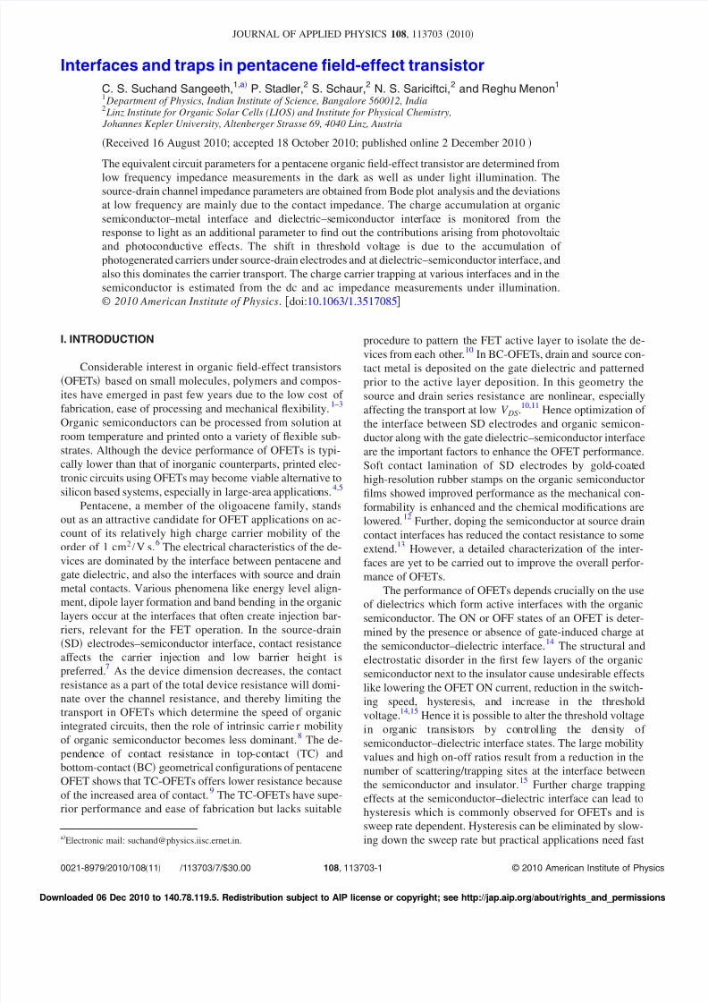
The pentacene OFETs are fabricated in the bottom-gate,TC conguration, as schematically depicted in Fig.1 a . Forthe device fabrication, aluminum150 nm is evaporated onglass and then partly oxidized electrochemically at a constantcurrent density of 0.6 mA cm−2 in 0.01 M citric acidsolution.36 The oxidation is stopped when the layer thicknessexceeds 85 nm. The alumina layer thickness is checked usingcapacitance and cross-section scanning electron microscopy
SEM measurements. After rinsing the oxide and treating itwith water at 80 °C, it is dried in vacuum at 150 °C. Poly-methyl methacrylate PMMA Aldrich, M w=996 000
GPC is used to passivate the oxide-surface,37 therefore a 40nm layer of PMMA100 ppm solution in acetoneis spun at1500 rpm. This dielectric bilayer exhibits a geometrical ca-pacitance of 35 nF cm−2 with a breakdown voltage in therange of 5 MV cm−1. Further PMMA gate dielectric helps inminimizing the hysteresis due to the charge trapping at thedielectric–pentacene interface.
Pentacenepurchased from Aldrich and cleaned in a fur-ther sublimation stepis evaporated on top of the dielectric at0.5 Ås−1 rate, and at a substrate temperature of 50 °C in a
hot wall epitaxy system.38 70 nm gold SD contacts areevaporated using a shadow mask, with 95m channellength L and 2 mm channel widthW , to complete thefabrication of the transistor, and ready for the complementelectrical and optical characterization.
The I -V characteristics of the devices under applied gavoltage were measured using Keithley SourcemetersModelKe-2400 and Ke-2611. The measurements were performed
in a Janis continuous ow optical cryostat under 10−2
Torrvacuum to avoid exposure to ambient conditions. A lockamplier based technique was used to nd the low frequeac impedance across the SD channel of the OFET. An apppriate dc biasV DS together with a superposed ac small signal 50 mV is applied across the SD electrodes of the OFEand the complex ac voltage responses are measured usinlock-in amplier SR-830 and a resistor-divider as describedelsewhere.31 Further, the pentacene OFET was characterizeunder monochromatic light irradiation at a wavelength532 nm using a diode laserModel Roithner-Lasetechnikand the corresponding values of the impedance are also msured. The devices were stable during the measurement terval under illumination, and bias-stress degradation effectwere negligible.39
III. RESULTS AND DISCUSSIONS
The transfer characteristics of the pentacene OFETplotted in Fig.1 b . The room temperature on-off ratio isfound to be 200. The mobility is calculated in the lineregime, using the relation:
I DS = W
LC i V GS − V T V DS, 1
where is the mobility,C i is the capacitance per unit area ofthe gate dielectric,V T is the threshold voltage, andW , L arethe channel width and length, respectively. The mobilityroom temperature is 0.08 cm2/ V s. The OFETs showednegligible hysteresis in the transfer characteristicssee Fig.1 b inset. This weak hysteresis indicates that a signicanumber of traps are in the shallow levels, and in case of dlevel traps the hysteresis is expected to be larger; howevthis needs more detailed investigation in future.
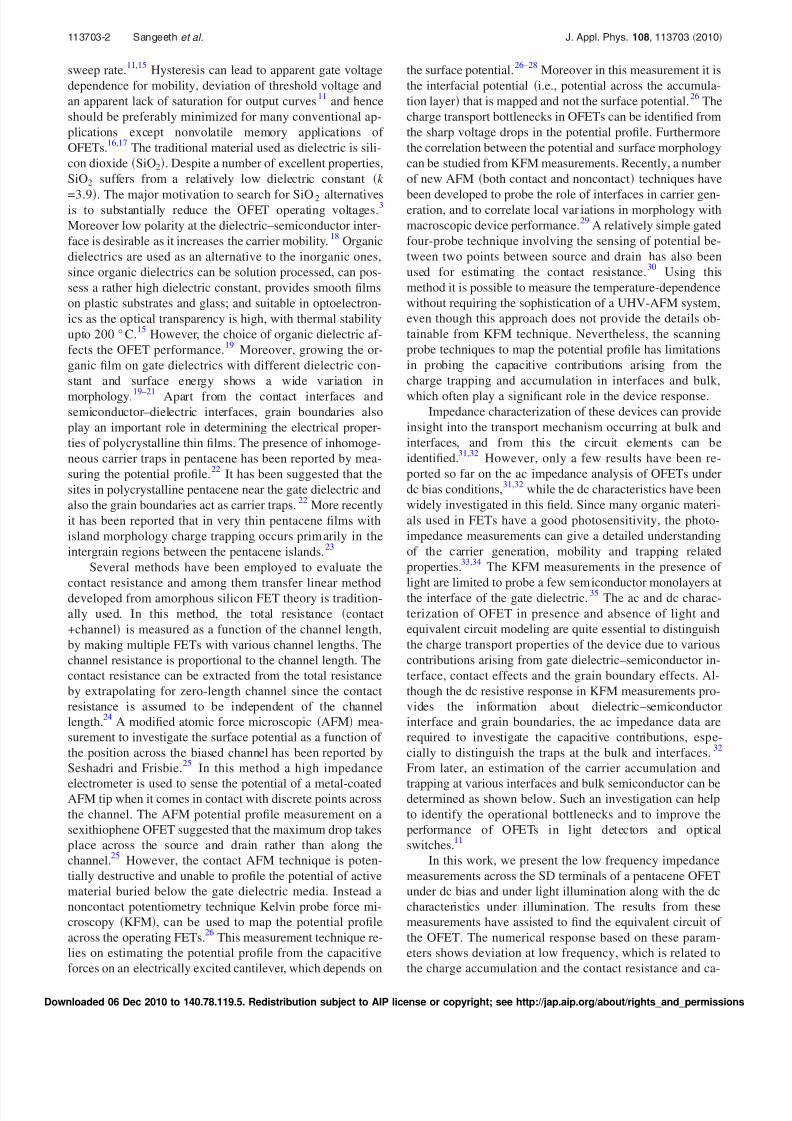
In Fig.2 a , the transfer curvesV DS =−8 V of the pen-tacene OFET in the dark and under a monochromatic li532 nm of various intensities are presented. The absorptio
spectrum of evaporated pentacene of 50 nm thickness
shown in the inset of Fig.2 a . Pentacene is excited at 2.33eV that is above the transport gap at 2.2 eV. The photogneration causes the increase in the drain current, e.g., bfactor of 22 at 2 mW/ cm2 light intensity. In the experi-ments, the light intensity was varied from 0.4 16 mW/ cm2. Large number of excitons, subsequently eletrons and holes, are generated when photons of energy eqto or higher than the band-gap are absorbed, and this cauthe increase in drain current. As the illumination intensityincreased, the drain current also increases, since the numof photogenerated carriers increases with the intensity light.34 Alongside with the gate bias the effect of light offean additional control for the charge carrier generation in
FIG. 1. Color online a Schematic diagram of the pentacene OFET.bTransfer characteristics of pentacene OFET in dark. Inset shows the hyster-esis in the transfer characteristics.
113703-3 Sangeeth et al. J. Appl. Phys. 108 , 113703 2010
Downloaded 06 Dec 2010 to 140.78.119.5. Redistribution subject to AIP license or copyright; see http://jap.aip.org/about/rights_and_permissions
8/7/2019 Interface and Traps in Pentacene Organic Field-effect Transistor
http://slidepdf.com/reader/full/interface-and-traps-in-pentacene-organic-field-effect-transistor 4/7
transistor.33 The photoinduced response of the OFET is ex-plained in terms of photoconductivity and photovoltaic ef-fects. Photoconductivity effect causes an increase in thedrain current when the OFET is in the off state, whereasphotovoltaic effect is responsible for the shift in its switch-onvoltage V on and threshold voltage V T , underillumination.40 When the OFET is in the off state, the in-crease in current is relatively small with the optical power,and the photocurrent is expressed by the linear relationship41
I ph, pc = q p pE WD = BP opt , 2
wherep is the carrier density,E is the electric eld in the
channel,W is the gate width,D is the depth of absorptionregion,P opt is the incident optical power, andB is a propor-tionality constant. The photocurrent in the off state is there-fore directly proportional to the incident light intensity, asshown in Fig.2 b .
When the device is in the on state, the photovoltageinduced by the accumulation of large number of electronsunder the source electrode or at the interface between thesemiconductor and gate dielectric gives rise to a signicantincrease in current. Among the photogenerated carriers in thepentacene channel, produced by the absorption of light, holeseasily ow to the drain electrode due to higher mobility,whereas electrons accumulate under the source electrode or
at the gate dielectric due to the lower mobility.34 These ac-cumulated electrons effectively lower the potential barrbetween the source and the semiconductor channel, leadto a shift in the switch-on voltage and threshold voltage, ashown in Fig.2 a .40 The shift in switch-on voltageV onsuggests that more number of photogenerated carriers being trapped at the interfaces. The shift in threshold volt
V T toward positive voltages shows logarithmic variati
with light intensity as shown in the inset of Fig.2 b , andthis is in agreement with model used in the data analysisin Eq. 3 . The photocurrent caused by photovoltaic effect isgiven by the following expression:42
I ph, pv = G M V T =Ak BT
qln 1 + q P opt
I pd hc, 3
where is the quantum efciency,q is the elementarycharge,I pd is the dark current for electrons,hc / is the pho-ton energy,G M is the transconductance,V T is the thresholdvoltage shift, andA is a tting parameter. The photocurrenas a function of incident optical intensity under the turnV GS =−12 V and turn-off V GS =−1.5 V states atV DS =
−8 V is shown in Fig.2 b . The t to the data for the turn-off condition shows a linear dependence, whereas the turncondition clearly shows the characteristic logarithmic behior, as given by Eq.3 .
The threshold voltage can be associated with the chargtrapped in interface states and the injection barrier at souelectrode; and it is possible to estimate the upper limit for density of hole trapping interface statesN I from43
N I =− Q I
e= −C i
eV T − m − S + V inj − C i
eV T , 4
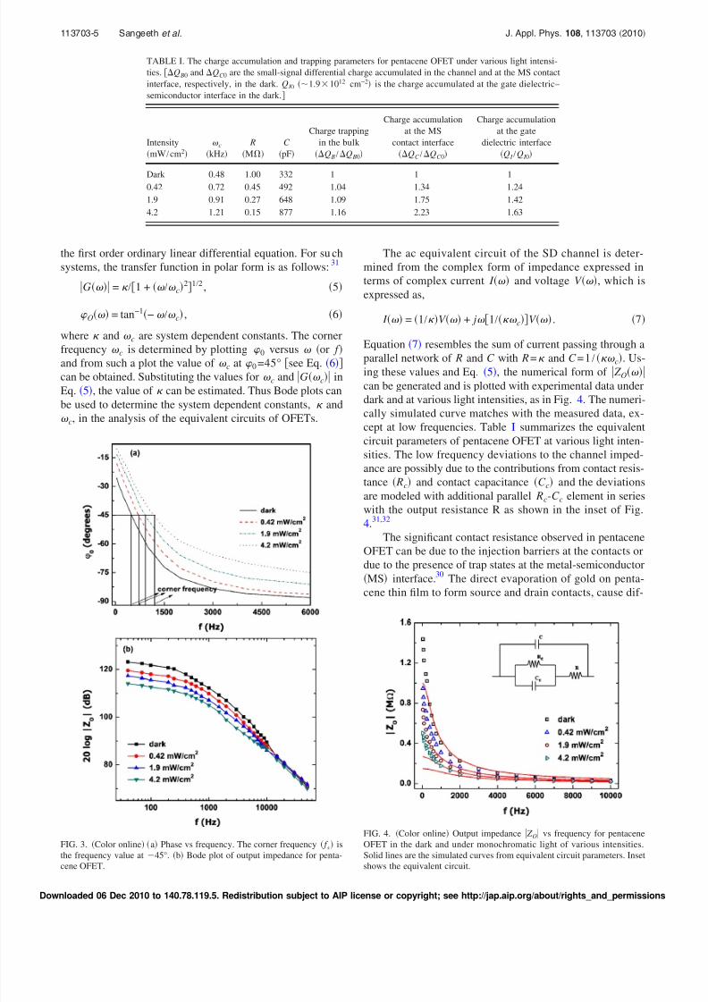
where m − S is the difference between gate and organisemiconductor workfunctions,Q I is the trapped charges inthe interface states at the semiconductor-dielectric boundaand V inj is a term that depends on the injecting contact. surface charge density of 1.91012 cm−2 accounts f or theobserved threshold voltage −8.6 V in the dark.43 How-ever, the actual value of N I can be smaller. Upon illumina-tion, the threshold voltage shifts toward positive voltages the increase in carrier density can be estimated from: N I =C i V T / e. The charge accumulation at various light intensties is presented in TableI.
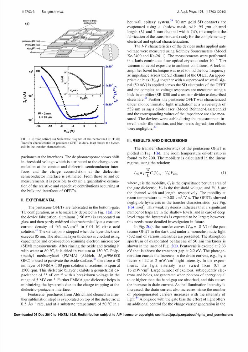
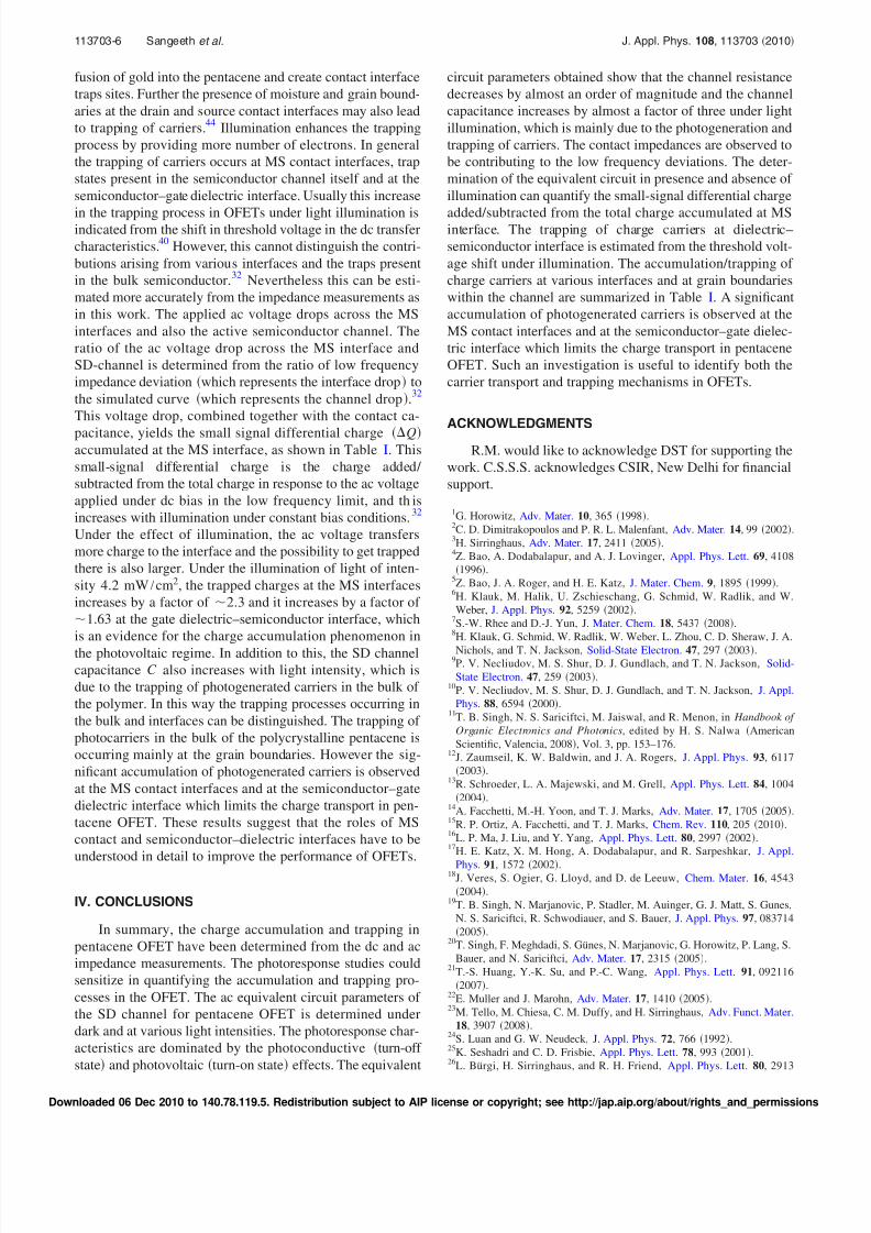
The impedance characterization of these devices und
dc bias and under light illumination is essential for a coprehensive understanding of the equivalent circuit, anddevelop theoretical models for injection and transport in ganic devices. Usually Bode plot analysis isbeing carriedout to understand the ac response of the FET.31 The phasevalue 0 is plotted as a function of frequency in Fig.3 aand the magnitude of the complex SD channel impedan Z O, represented in units of decibels, is plotted as a functiof logf in Fig.3 b , for different intensities of incident lighand also under dark condition. The negative phase angle creases in magnitude while increasing the frequency. Thigh frequency asymptote has a slope of nearly20 dB/ decade, as known in linear time-invariant system that follo
FIG. 2. Color online a Transfer characteristics of pentacene OFET in thedark and under illumination at various intensities. Inset shows the absorptionspectrum of pentacene50 nm thick lm. b Photocurrent as a function of incident light intensity under turn-on and turn-off states. Solid lines are tsto Eqs. 2 and 3 . Inset: threshold voltage shift vs light intensity.
113703-4 Sangeeth et al. J. Appl. Phys. 108 , 113703 2010
Downloaded 06 Dec 2010 to 140.78.119.5. Redistribution subject to AIP license or copyright; see http://jap.aip.org/about/rights_and_permissions
8/7/2019 Interface and Traps in Pentacene Organic Field-effect Transistor
http://slidepdf.com/reader/full/interface-and-traps-in-pentacene-organic-field-effect-transistor 5/7
the rst order ordinary linear differential equation. For suchsystems, the transfer function in polar form is as follows:31
G = / 1 + / c2 1/2, 5
O = tan−1 − / c , 6
where and c are system dependent constants. The corner
frequency c is determined by plotting 0 versus or f and from such a plot the value of c at 0=45° see Eq. 6can be obtained. Substituting the values for c and G c inEq. 5 , the value of can be estimated. Thus Bode plots canbe used to determine the system dependent constants, and
c, in the analysis of the equivalent circuits of OFETs.
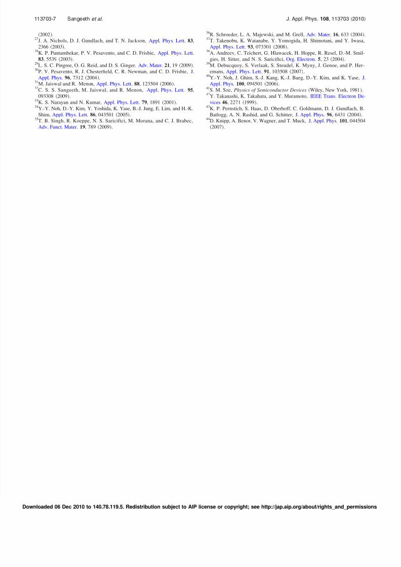
The ac equivalent circuit of the SD channel is detemined from the complex form of impedance expressedterms of complex currentI and voltageV , which isexpressed as,
I = 1/ V + j 1/ c V . 7
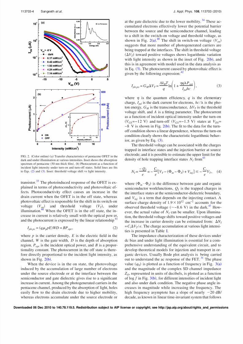
Equation 7 resembles the sum of current passing throughparallel network of R andC with R= andC =1/ c . Us-ing these values and Eq.5 , the numerical form of Z O
can be generated and is plotted with experimental data undark and at various light intensities, as in Fig.4. The numeri-cally simulated curve matches with the measured data, cept at low frequencies. TableI summarizes the equivalentcircuit parameters of pentacene OFET at various light intsities. The low frequency deviations to the channel impance are possibly due to the contributions from contact retance Rc and contact capacitanceC c and the deviationsare modeled with additional parallelRc-C c element in serieswith the output resistance R as shown in the inset of Fi
4.31,32
The signicant contact resistance observed in pentaceOFET can be due to the injection barriers at the contactsdue to the presence of trap states at the metal-semiconductoMS interface.30 The direct evaporation of gold on penta
cene thin lm to form source and drain contacts, cause d
TABLE I. The charge accumulation and trapping parameters for pentacene OFET under various light intensi-ties. Q B0 and QC 0 are the small-signal differential charge accumulated in the channel and at the MS contactinterface, respectively, in the dark.Q I 0 1.9 1012 cm−2 is the charge accumulated at the gate dielectric–semiconductor interface in the dark.
IntensitymW/ cm2
c
kHz R
MC pF
Charge trappingin the bulk
Q B / Q B0
Charge accumulationat the MS
contact interfaceQ C / Q C 0
Charge accumulationat the gate
dielectric interfaceQ I / Q I 0
Dark 0.48 1.00 332 1 1 10.42 0.72 0.45 492 1.04 1.34 1.241.9 0.91 0.27 648 1.09 1.75 1.424.2 1.21 0.15 877 1.16 2.23 1.63
FIG. 3. Color online a Phase vs frequency. The corner frequency f c isthe frequency value at45°. b Bode plot of output impedance for penta-cene OFET.
FIG. 4. Color onlineOutput impedance Z O vs frequency for pentaceneOFET in the dark and under monochromatic light of various intensitSolid lines are the simulated curves from equivalent circuit parameters. Ishows the equivalent circuit.
113703-5 Sangeeth et al. J. Appl. Phys. 108 , 113703 2010
Downloaded 06 Dec 2010 to 140.78.119.5. Redistribution subject to AIP license or copyright; see http://jap.aip.org/about/rights_and_permissions
8/7/2019 Interface and Traps in Pentacene Organic Field-effect Transistor
http://slidepdf.com/reader/full/interface-and-traps-in-pentacene-organic-field-effect-transistor 6/7
8/7/2019 Interface and Traps in Pentacene Organic Field-effect Transistor
http://slidepdf.com/reader/full/interface-and-traps-in-pentacene-organic-field-effect-transistor 7/7
2002 .27J. A. Nichols, D. J. Gundlach, and T. N. Jackson,Appl. Phys. Lett.83 ,
2366 2003.28K. P. Puntambekar, P. V. Pesavento, and C. D. Frisbie,Appl. Phys. Lett.
83 , 5539 2003.29L. S. C. Pingree, O. G. Reid, and D. S. Ginger,Adv. Mater.21 , 19 2009 .30P. V. Pesavento, R. J. Chestereld, C. R. Newman, and C. D. Frisbie,J.
Appl. Phys.96 , 7312 2004 .31M. Jaiswal and R. Menon,Appl. Phys. Lett.88 , 123504 2006 .32C. S. S. Sangeeth, M. Jaiswal, and R. Menon,Appl. Phys. Lett.95 ,
093308 2009 .33K. S. Narayan and N. Kumar,Appl. Phys. Lett.79 , 1891 2001.34Y.-Y. Noh, D.-Y. Kim, Y. Yoshida, K. Yase, B.-J. Jung, E. Lim, and H.-K.
Shim,Appl. Phys. Lett.86 , 043501 2005.35T. B. Singh, R. Koeppe, N. S. Sariciftci, M. Morana, and C. J. Brabec,
Adv. Funct. Mater.19 , 789 2009 .
36R. Schroeder, L. A. Majewski, and M. Grell,Adv. Mater.16 , 633 2004 .37T. Takenobu, K. Watanabe, Y. Yomogida, H. Shimotani, and Y. Iwas
Appl. Phys. Lett.93 , 073301 2008 .38A. Andreev, C. Teichert, G. Hlawacek, H. Hoppe, R. Resel, D.-M. Sm
gies, H. Sitter, and N. S. Sariciftci,Org. Electron.5 , 23 2004.39M. Debucquoy, S. Verlaak, S. Steudel, K. Myny, J. Genoe, and P. H
emans,Appl. Phys. Lett.91 , 103508 2007 .40Y.-Y. Noh, J. Ghim, S.-J. Kang, K.-J. Baeg, D.-Y. Kim, and K. Yase,J.
Appl. Phys.100 , 094501 2006.41S. M. Sze,Physics of Semiconductor Devices Wiley, New York, 1981.42Y. Takanashi, K. Takahata, and Y. Muramoto,IEEE Trans. Electron De-
vices46 , 2271 1999 .43K. P. Pernstich, S. Haas, D. Oberhoff, C. Goldmann, D. J. Gundlach,
Batlogg, A. N. Rashid, and G. Schitter,J. Appl. Phys.96 , 6431 2004.44D. Knipp, A. Benor, V. Wagner, and T. Muck,J. Appl. Phys.101 , 044504
2007.
113703-7 Sangeeth et al. J. Appl. Phys. 108 , 113703 2010
l d d d b b l h h b h d