interconnect-based design methodologies for three
TRANSCRIPT

Interconnect-Based Design Methodologies for
Three-Dimensional Integrated Circuits
by
Vasileios F. Pavlidis
Submitted in Partial Fulfillment
of the
Requirements for the Degree
Doctor of Philosophy
Supervised by
Professor Eby G. Friedman
Department of Electrical and Computer Engineering
The College
School of Engineering and Applied Sciences
University of Rochester
Rochester, New York
2008

ii
Dedication
To the memory of my beloved grandfathers, Athanasios Theophilidis and Vasileios Pavlidis

iii
Curriculum Vitae
Vasileios F. Pavlidis was born in Kavala, Greece, in 1976. He received the B.S. and M.Eng. in
electrical and computer engineering from the Democritus University of Thrace, Xanthi, Greece,
in 2000 and 2002, respectively. From 2000 to 2002, he was with INTRACOM S.A., Athens,
Greece. In August 2002, he joined the electrical and computer engineering department at the
University of Rochester, where he is working toward the Ph.D. degree under the supervision of
Professor Eby G. Friedman. He received the M.Sc. from the electrical and computer engineering
department at the University of Rochester in 2003. During summer 2007, he was with Synopsys
Inc. as a summer intern. His present research interests are in the area of interconnect modeling, 3-
D integration, networks-on-chip, and related design issues in VLSI.

iv
Acknowledgments
First and above all, I would like to express my sincere gratitude to my advisor Professor Eby G.
Friedman for his guidance and encouragement during the ragged path of the PhD program. I
firmly believe that next to him, I was taught the fundamentals to perform cutting edge research
and prepare myself for a successful professional career, hopefully, as an academician. His
perspicacity, patience, persistence, intellectuality, and, in general, his thirst for perfection have
immensely contributed to my evolution as a young researcher. I consider myself lucky to work
for him and I honestly would not exchange my years as his advisee for any other Professor
around this globe. Thank you Professor!
I would also like to thank Professors David Quesnel, Joel Seiferas, and Michael Huang for
their service on my proposal and defense committees and their helpful suggestions. I am grateful
to Professor Paul Ampadu for his assistance and encouragement during my job search process.
Special thanks to Professors Volkan Kursun, Yehea Ismail, and Dimitrios Soudris who
generously provided me with valuable letters of recommendation. I am also particularly thankful
to Dr. Khalid Rahmat, my manager while I was interning at Synopsys, for introducing me to the
basics of timing analysis and sharing much of his knowledge and experience on design
automation. The indispensable support of Dr. Yunliang Zhu, Lin Zhang, and Professor Hui Wu
during the testing of the 3-D circuit is greatly appreciated.
In addition, I would like to thank a few people who significantly helped me over these years.
My lab mates with whom I want to believe that we have opened paths of friendship rather than
“race tracks” as the modern abusive research culture would dictate. Dr. Mikhail Popovich, Dr.
Guoging Chen, Jonathan Rosenfeld, Emre Salman, Renatas Jakushokas, Ioannis Savidis, and
Selcuk Kose, I thank you and I hope you had as much fun as I had. Next to them, I am indebted to

v
the one and only, Ms. RuthAnn Williams (the pillar of the HPIC lab) for her constant willingness
to help me with non-technical issues and, more importantly, for being the thesaurus of the
American slang and the myriads of philosophical discussions we had through these years.
Last but not least, I would like to thank Dr. Dimitrios Velenis for prodding me at certain
difficult moments of my PhD experience and his encouragement to participate in professional
activities, which otherwise I would completely ignore. His advice and, primarily, his friendship
are deeply acknowledged.
This research was supported in part by the National Science Foundation under Contract No.
CCF-0541206, grants from the New York State Office of Science, Technology & Academic
Research to the Center for Advanced Technology in Electronic Imaging Systems, and by grants
from Intel Corporation, Eastman Kodak Company, and Freescale Semiconductor Corporation,
and foundry support from the MIT Lincoln Laboratories.

vi
Abstract
Three-dimensional (3-D) or vertical integration is a potent design paradigm to overcome the
existing interconnect bottleneck in integrated systems. The major advantages of this emerging
technology are the inherent reduction in wirelength and the ability to integrate heterogeneous
circuits within a multi-plane system. To exploit these advantages, however, several challenges
across different design abstraction levels, such as the architecture, physical, and technology
levels, need to be overcome. In this dissertation, several issues affecting the design of 3-D
circuits, primarily at the physical and architecture levels, are addressed.
Considering the importance of the interplane communication within a 3-D circuit, novel design
methodologies and algorithms for the interplane interconnects are proposed in this dissertation.
Algorithms for placing the interplane vias are proposed to lower the interconnect delay. Both
two- and multi-terminal nets are considered. The proposed methodologies are the first to consider
the heterogeneous nature of 3-D circuits; specifically, the impedance characteristics of the
interplane vias.
Low latency interconnect, as compared to the long global wires, and the added design freedom
due to the third dimension enable innovative topologies for on-chip networks. Several topologies
for 3-D networks-on-chip that exhibit considerably enhanced performance as compared to 2-D
topologies are proposed. Accurate analytic models that describe the interconnect delay and power
within these networks have been developed.
The important global signaling issue of synchronization in 3-D circuits has been investigated
for the first time. Several commonly used 2-D clock distribution architectures are combined into
new 3-D synchronization network topologies. The design of these clock distribution networks and

vii
measurements from a 3-D test circuit are presented in the last part of this dissertation.
Experimental results demonstrate successful operation at 1.4 GHz.
Summarizing, throughout this research thesis, many interconnect related problems in 3-D
circuits have been addressed. Efficient and accurate solutions for these issues are proposed. These
solutions are supported by results from an experimental 3-D test circuit. The proposed design
methodologies described in this dissertation are intended to strengthen 3-D design capabilities,
making this fascinating technology a promising solution for future integrated systems.

viii
Contents
Dedication ........................................................................................................................................ ii
Curriculum Vitae ............................................................................................................................ iii
Acknowledgments .......................................................................................................................... iv
Abstract ........................................................................................................................................... vi
Contents ........................................................................................................................................ viii
List of Figures ............................................................................................................................... xiii
List of Tables .............................................................................................................................. xxvi
Chapter 1. Introduction ................................................................................................................ 1
1.1. From the Integrated Circuit to the Computer ................................................................. 3
1.2. Interconnects; an old Friend ........................................................................................... 6
1.3. Three-Dimensional or Vertical Integration .................................................................. 10
1.3.1. Opportunities for Three-Dimensional Integration .................................................... 11
1.3.2. Challenges for Three-Dimensional Integration ........................................................ 14
1.4. Dissertation Organization ............................................................................................. 17
Chapter 2. Manufacturing of 3-D Packaged Systems ................................................................ 21
2.1. Three-Dimensional Integration ..................................................................................... 21
2.1.1. System-in-Package ................................................................................................... 23
2.1.2. Three-Dimensional Integrated Circuits .................................................................... 24
2.2. System-on-Package ...................................................................................................... 25
2.3. Technologies for System-in-Package ........................................................................... 29
2.3.1. Wire Bonded System-in-Package............................................................................. 30
2.3.2. Peripheral Vertical Interconnects ............................................................................. 32

ix
2.3.3. Area Array Vertical Interconnects ........................................................................... 35
2.3.4. Metallizing the Walls of an SiP................................................................................ 37
2.4. Cost Issues for 3-D Integrated Systems ........................................................................ 39
2.5. Summary ...................................................................................................................... 42
Chapter 3. 3-D Integrated Circuit Fabrication Technologies ..................................................... 44
3.1. Monolithic 3-D ICs ....................................................................................................... 45
3.1.1. Stacked 3-D ICs ....................................................................................................... 46
3.1.2. 3-D Fin-FETs ........................................................................................................... 54
3.2. 3-D ICs with Through Silicon or Interplane Vias ........................................................ 57
3.3. Contactless 3-D ICs ...................................................................................................... 63
3.3.1. Capacitively Coupled 3-D ICs ................................................................................. 63
3.3.2. Inductively Coupled 3-D ICs ................................................................................... 66
3.4. Vertical Interconnects for 3-D ICs ............................................................................... 67
3.4.1. Electrical Characteristics of Through Silicon Vias .................................................. 74
3.5. Summary ...................................................................................................................... 76
Chapter 4. Interconnect Prediction Models ............................................................................... 78
4.1. Interconnect Prediction Models for 2-D Circuits ......................................................... 79
4.2. Interconnect Prediction Models for 3-D ICs ................................................................ 82
4.3. Projections for 3-D ICs ................................................................................................. 88
4.4. Summary ...................................................................................................................... 94
Chapter 5. Physical Design Techniques for 3-D ICs ................................................................. 95
5.1. Floorplanning Techniques ............................................................................................ 95
5.1.1. Single versus Multi-Step Floorplanning for 3-D ICs ............................................... 97
5.1.2. Multi-Objective Floorplanning Techniques for 3-D ICs ........................................ 101
5.2. Placement Techniques ................................................................................................ 104

x
5.2.1. Multi-Objective Placement for 3-D ICs ................................................................. 105
5.3. Routing Techniques .................................................................................................... 108
5.4. Layout Tools ............................................................................................................... 113
5.5. Three-Dimensional FPGAs ........................................................................................ 115
5.6. Summary .................................................................................................................... 123
Chapter 6. Thermal Management Techniques ......................................................................... 125
6.1. Thermal Analysis of 3-D ICs ..................................................................................... 126
6.1.1. Closed-Form Temperature Expressions ................................................................. 127
6.1.2. Compact Thermal Models ...................................................................................... 135
6.1.3. Mesh Based Thermal Models ................................................................................. 137
6.2. Thermal Management Techniques without Thermal Vias ......................................... 139
6.2.1. Thermal-Driven Floorplanning .............................................................................. 140
6.2.2. Thermal-Driven Placement .................................................................................... 147
6.3. Thermal Management Techniques Employing Thermal Vias .................................... 151
6.3.1. Region Constrained Thermal Via Insertion ........................................................... 151
6.3.2. Thermal Via Planning Techniques ......................................................................... 155
6.3.3. Thermal Wire Insertion .......................................................................................... 161
6.4. Summary .................................................................................................................... 163
Chapter 7. Timing Optimization for Two-Terminal Interconnects .......................................... 166
7.1. Interplane Interconnect Models .................................................................................. 167
7.2. Two-Terminal Nets with a Single Interplane Via....................................................... 173
7.2.1. Elmore delay model of an interplane interconnect ................................................. 173
7.2.2. Interplane Interconnect Delay ................................................................................ 176
7.2.3. Optimum Via Location .......................................................................................... 178
7.2.4. Improvement in Interconnect Delay ....................................................................... 182

xi
7.3. Two-Terminal Interconnects with Multiple Interplane Vias ...................................... 185
7.3.1. Two-Terminal Via Placement Heuristic ................................................................ 190
7.3.2. Two-Terminal Via Placement Algorithm .............................................................. 194
7.3.3. Application of the Via Placement Technique ........................................................ 195
7.4. Summary .................................................................................................................... 202
Chapter 8. Timing Optimization for Multi-Terminal Interconnects ........................................ 204
8.1. Timing-Driven Via Placement for Interplane Interconnect Trees .............................. 204
8.2. Multi-Terminal Interconnect Via Placement Heuristics ............................................. 208
8.2.1. Interconnect Trees .................................................................................................. 209
8.2.2. Single Critical Sink Interconnect Trees ................................................................. 210
8.3. Via Placement Algorithms for Interconnect Trees ..................................................... 212
8.3.1. Interconnect Tree Via Placement Algorithm (ITVPA) .......................................... 212
8.3.2. Single Critical Sink Interconnect Tree Via Placement Algorithm (SCSVPA) ...... 213
8.4. Via Placement Results and Discussion ....................................................................... 214
8.5. Summary .................................................................................................................... 219
Chapter 9. 3-D Topologies for Networks-on-Chip .................................................................. 221
9.1. 3-D NoC Topologies .................................................................................................. 223
9.2. Zero-Load Latency for 3-D NoC ................................................................................ 224
9.3. Power Consumption in 3-D NoC................................................................................ 230
9.4. Performance and Power Analysis for 3-D NoC ......................................................... 233
9.4.1. Parameters of 3-D Networks-on-Chip .................................................................... 233
9.4.2. Performance Tradeoffs for 3-D NoC ..................................................................... 235
9.4.3. Power Consumption in 3-D NoC ........................................................................... 245
9.5. Summary .................................................................................................................... 251
Chapter 10. Case Study: Clock Distribution Networks for 3-D ICs...................................... 253

xii
10.1. MITLL 3-D IC Fabrication Technology .................................................................... 254
10.2. 3-D Circuit Architecture ............................................................................................. 259
10.3. Clock Signal Distribution in 3-D Circuits .................................................................. 264
10.3.1. Timing Characteristics of Synchronous Circuits ............................................... 264
10.3.2. Clock Distribution Network Structures within the Test Circuit ........................ 267
10.4. Experimental Results .................................................................................................. 273
10.5. Summary .................................................................................................................... 280
Chapter 11. Conclusions ........................................................................................................ 282
Chapter 12. Future Work ....................................................................................................... 286
12.1. Power Distribution Networks for 3-D ICs .................................................................. 287
12.2. Signal Integrity in the Vertical Direction ................................................................... 290
12.3. Thermal-Aware Packet Routing for 3-D NoC ............................................................ 293
12.4. Summary .................................................................................................................... 295
References .................................................................................................................................... 296
Appendix A: Enumeration of Gate Pairs in a 3-D IC .............................................................. 330
Appendix B: Formal Proof of Optimum Single Via Placement .............................................. 332
Appendix C: Proof of the Two-Terminal Via Placement Heuristic ........................................ 333
Appendix D: Proof of Condition for Via Placement of Multi-Terminal Nets ......................... 337

xiii
List of Figures
Fig. 1-1 History of transistor generations and logic styles [8]. ................................................ 4
Fig. 1-2 The first planar integrated circuit [9]. ......................................................................... 5
Fig. 1-3 The 4004 Intel microprocessor [9].............................................................................. 6
Fig. 1-4 Interconnect architecture including local, semi-global, and global tiers. The metal
layers on each tier are of different thickness. ............................................................. 7
Fig. 1-5 Repeaters are inserted at specific distances to improve the interconnect delay. ......... 8
Fig. 1-6 Interconnect shielding to improve signal integrity, (a) single-sided and (b) double-
sided shielding. The shield and signal lines are illustrated by the grey and white
color, respectively. ...................................................................................................... 9
Fig. 1-7 Cross-section of a JMOS inverter [35]. .................................................................... 11
Fig. 1-8 Reduction in wire length where the original 2-D circuit is implemented in two and
four planes. ............................................................................................................... 12
Fig. 1-9 An example of a heterogeneous 3-D system-on-chip comprising sensor and
processing planes. ..................................................................................................... 13
Fig. 2-1 Three-dimensional stacked inverter [34]. ................................................................. 22
Fig. 2-2 Examples of SiP, (a) wire bonded SiP [42], (b) solder balls at the perimeter of the
planes [43], (c) area array vertical interconnects, and (d) interconnects on the faces
of the SiP [44]. .......................................................................................................... 23
Fig. 2-3 Various communication schemes for 3-D ICs [45], (a) short through silicon vias, (b)
inductive coupling [36], and (c) capacitive coupling [46]. ....................................... 25
Fig. 2-4 (a) A typical SoP [48] and (b) relation of SoP, SiP, 3-D IC, and SoC. .................... 27
Fig. 2-5 Manufacturing and design challenges for three-dimensional integration. ................ 28

xiv
Fig. 2-6 System miniaturization through the integration of sophisticated 3-D ICs [48]. ....... 28
Fig. 2-7 Wire bonded SiP, (a) dissimilar dies with multiple row bonding, (b) wire bonded
stack delimited by spacer, (c) SiP with die-to-die and die-to-package wire bonding,
and (d) top view of wire bonded SiP [42]. ................................................................ 30
Fig. 2-8 SiP with peripheral connections, (a) solder balls [43], (b) through-hole via and
spacers [53], and (c) through-hole via in a PCB frame structure [54]. ..................... 33
Fig. 2-9 Basic manufacturing phases of an SiP, (a) interposer bumping and solder ball
deposition, (b) die attachment, (c) plane stacking, and (d) epoxy underfill for
enhanced reliability. .................................................................................................. 34
Fig. 2-10 Cross-section of the SiP after removing the mold, (a) the SiP encapsulated in epoxy
resin, (b) sawing to expose the metal traces, and (c) sawing to expose the bonding
wires [63]. ................................................................................................................. 39
Fig. 3-1 Typical interconnects paths for (a) wire bonded SiP, (b) SiP with solder balls, and
(c) 3-D IC with through silicon vias (TSVs). ........................................................... 45
Fig. 3-2 Cross-section of a stacked 3-D IC with a planarized heat shield (PHS) used to avoid
degradation of the transistor characteristics on the first plane due to the temperature
of the fabrication processes [67]. .............................................................................. 47
Fig. 3-3 Cross-section of a stacked 3-D IC with a PMOS device on the bottom plane and an
NMOS device in recrystallized silicon on the second plane [68]. ............................ 48
Fig. 3-4 Processing steps for laterally crystallized TFT based on Ge-seeding. (a) Deposition
of amorphous silicon, (b) creating seeding windows, (c) deposition of seeding
materials, (d) producing silicon islands, and (e) processing of TFTs [73]. .............. 51
Fig. 3-5 Processing steps for vertical and lateral growth of 3-D SOI devices [74]. ............... 52
Fig. 3-6 Basic processing steps for a 3-D inverter utilizing the local clustering approach
[76]. ........................................................................................................................... 54

xv
Fig. 3-7 3-D stacked Fin-CMOS device [80]. ........................................................................ 55
Fig. 3-8 Processing steps for 3-D stacked fin-CMOS, (a) formation of the gate mask, (b)
etching step to form the stacked fin, (c) deposition of oxide and polysilicon layers,
(d) ion implantation to form drain and source regions, (e) etching step to generate
contact openings, and (f) metallization of the contact openings [80]. ...................... 57
Fig. 3-9 Typical fabrication steps for a 3-D IC process, (a) wafer preparation, (b) TSV
etching, (c) wafer thinning, bumping, and handle wafer attachment, (d) wafer
bonding, and (e) handle wafer removal. ................................................................... 58
Fig. 3-10 Metal-to-metal bonding; (a) square bumps and (b) conic bumps for improved
bonding quality [91]. ................................................................................................ 63
Fig. 3-11 Capacitively coupled 3-D IC; the large plate capacitors are utilized for power
transfer, while the small plate capacitors are used for signal propagation [46]. ....... 65
Fig. 3-12 Inductively coupled 3-D ICs. The galvanic connections are used for power delivery
[99]. ........................................................................................................................... 67
Fig. 3-13 Through silicon via formation and filling after wafer thinning (“via last” approach).
68
Fig. 3-14 Through silicon via shapes, (a) straight and (b) tapered. .......................................... 69
Fig. 3-15 A schematic representation of the scallops formed due to the time-multiplexed
nature of the BOSCH process. .................................................................................. 70
Fig. 3-16 Schematic representation of poor TSV filling resulting in void formation (a) large
void at the bottom and (b) seam void. ...................................................................... 73
Fig. 3-17 Structure of partial TSV and related materials [111]. ............................................... 73
Fig. 3-18 Electrical model of a TSV [113]. .............................................................................. 75
Fig. 4-1 An example of the method used to determine the distribution of the interconnect
length. Group NA includes one gate, group NB includes the gates located at a distance

xvi
smaller than l (encircled by the dashed curve), and NC is the group of gates at
distance l from group NA (encircled by the solid curve). In this example, l = 4 (the
distance is measured in gate pitches) [120]. ............................................................. 80
Fig. 4-2 An example of the method used to determine the interconnect length distribution in
3-D circuits, (a) partial manhattan hemisphere and (b) cross-section of the partial
manhattan hemisphere along e-e’. The gates in NB and NC are shown with light and
dark gray tones, respectively [125]. .......................................................................... 83
Fig. 4-3 Example of starting and non-starting gates. Gates P and Q can be starting gates
while S is a non-starting gate [125]. ......................................................................... 84
Fig. 4-4 Possible vertical interconnections for two cells with each cell containing n gates
[129]. ......................................................................................................................... 87
Fig. 4-5 Interconnect length distribution for a 2-D and 3-D IC [122]. ................................... 89
Fig. 4-6 Variation of gate pitch, total interconnect length, and interconnect power
consumption with the number of planes [138]. ........................................................ 91
Fig. 5-1 Area and volume upper bounds for two- and three-dimensional slicing floorplans are
depicted by the solid and dashed curve, respectively, for different shape aspect ratio.
Vtotal (Atotal) and Vmax (Amax) are the total and maximum volume (area) respectively of
a 3-D (2-D) system [152]. ......................................................................................... 97
Fig. 5-2 Floorplanning strategies for 3-D ICs, (a) single step approach and (b) multi-step
approach [155]. ......................................................................................................... 98
Fig. 5-3 Design flow of the microarchitectural floorplanning process for 3-D
microprocessors [158]. ........................................................................................... 103
Fig. 5-4 White space detection is illustrated by the white regions [171]. ............................ 106
Fig. 5-5 Block placement of an SOP (a) an initial placement and (b) an increase in the total
area in the x and y directions to extend the area of the white spaces [171]. ........... 107

xvii
Fig. 5-6 Channel alignment procedure to create the interplane routing channels [179]. ...... 109
Fig. 5-7 An SOP consisting of n planes. The vertical dashed lines correspond to vias between
the routing layers and the thick vertical solid lines correspond to through vias that
penetrate the device layers [182]. ........................................................................... 111
Fig. 5-8 Stages of a 3-D global routing algorithm [182]. ..................................................... 112
Fig. 5-9 Layout windows where different area markers are illustrated; (a) layout window for
plane 1 and (b) layout window for plane 2 (windows are not of the same scale). .. 114
Fig. 5-10 Typical FPGA architecture, (a) a 2-D FPGA, (b) a 2-D switch box, and (c) a 3-D
switch box. A routing track can connect three outgoing tracks in a 2-D SB, while in
a 3-D SB, a routing track can connect five outgoing routing tracks [189]. ............ 116
Fig. 5-11 Interconnects that span more than one logic block. Li denotes the length of these
interconnects and i is the number of LBs traversed by these wires. ....................... 117
Fig. 5-12 Interconnect delay for various number of physical planes [191], (a) average length
wires and (b) die edge length interconnects. ........................................................... 119
Fig. 5-13 Power dissipated by 2-D and 3-D FPGAs [191]. .................................................... 120
Fig. 5-14 Design flow of a three-dimensional FPGA-based placement and routing tool [197]. ..
................................................................................................................................ 122
Fig. 6-1 Thermal model of a 3-D circuit where one-dimensional heat transfer is assumed
[206]. ....................................................................................................................... 128
Fig. 6-2 Temperature increase in a 3-D circuit for different number of planes and power
densities [206]. ........................................................................................................ 131
Fig. 6-3 An example of the duality of thermal and electrical systems. ................................ 132
Fig. 6-4 Different vertical heat transfer paths in a 3-D IC [209]. ......................................... 133
Fig. 6-5 Maximum temperature vs. power density for 3-D ICs, SOI, and bulk CMOS [209].
The difference among the curves for the 3-D ICs is that the first curve (3-D

xviii
horizontal and vertical) includes thermal paths with a horizontal interconnect
segment while the second curve includes only interplane vias (only 3-D vertical
vias). ....................................................................................................................... 134
Fig. 6-6 Thermal model of a 3-D IC, (a) a 3-D tile stack, (b) one pillar of the stack, and (c)
an equivalent thermal resistive network. R1 and Rp correspond to the thermal
resistance of the thick silicon substrate of the first plane and the thermal resistance
of the package, respectively [211]. ......................................................................... 137
Fig. 6-7 A four plane 3-D circuit discretized into parallelepipeds. ...................................... 138
Fig. 6-8 Fundamental parallelepiped used to model thermal effects in a 3-D IC based on
FEM. ....................................................................................................................... 139
Fig. 6-9 Temperature cost function [217]............................................................................. 141
Fig. 6-10 A bucket structure example for a two plane circuit consisting of twelve blocks [217],
(a) a two plane 3-D IC, (b) a 2 × 2 bucket structure imposed on a 3-D IC, and (c) the
resulting bucket indices. ......................................................................................... 142
Fig. 6-11 Interplane moves, (a) an initial placement, (b) a z-neighbor swap between blocks a
and h, and (c) a z-neighbor move for block l from the first plane to the second plane.
................................................................................................................................ 143
Fig. 6-12 Mapping of a task graph onto physical PEs within a 3-D NoC [220]. ................... 147
Fig. 6-13 Thermal conductivity vs. thermal via density [227]. .............................................. 154
Fig. 6-14 Multilevel routing flow with thermal via planning [229]. ...................................... 158
Fig. 6-15 Various heat propagation paths within a 3-D grid [229]. ....................................... 158
Fig. 6-16 Routing grid for a two plane 3-D IC. Each horizontal edge of the grid is associated
with a horizontal wire capacity. Each vertical edge is associated with an interplane
via capacity. ............................................................................................................ 161

xix
Fig. 6-17 Impact of a thermal wire on the routing capacity of each grid cell. vi and vj denote
the capacity of the interplane vias for cell i and j, respectively. The horizontal cell
capacity is equal to the width of the boundary of the cells [234]. .......................... 162
Fig. 6-18 Flowchart of a temperature aware 3-D global routing technique [234]. ................. 163
Fig. 7-1 Global interconnect structures for impedance extraction, (a) three parallel metal
lines over a ground plane in a 2-D circuit and (b) three parallel metal lines
sandwiched between two ground planes in a 3-D circuit. ...................................... 168
Fig. 7-2 A three plane FDSOI 3-D circuit [139], [235]. Planes one and two are front-to-front
bonded, while planes two and three are front-to-back bonded. .............................. 169
Fig. 7-3 Capacitance extraction for an interplane via structure; (a) interplane via surrounded
by orthogonal metal layers and (b) capacitance values for various via sizes and
spacing values. ........................................................................................................ 170
Fig. 7-4 Capacitance extraction for an interplane via structure; (a) interplane via through
layers of dielectric and the bonding interface, surrounded by eight interplane vias
and (b) capacitance values for various via sizes and spacings. For all of the layers,
the same dielectric material is assumed (i.e., )2SiOid εεε == . ................................ 171
Fig. 7-5 Capacitance extraction for an interplane via structure; (a) interplane via through
silicon substrate, surrounded by a thin insulator layer and (b) capacitance values for
various via sizes and thicknesses of the insulator layer. ......................................... 172
Fig. 7-6 Two-terminal interplane interconnect with single via and the corresponding
electrical model. ...................................................................................................... 174
Fig. 7-7 An example of interconnect sizing. (a) An interconnect of minimum width, Wmin, (b)
uniform interconnect sizing W > Wmin, and (c) non-uniform interconnect sizing W =
f(l). .......................................................................................................................... 177

xx
Fig. 7-8 SPICE measurements of 50% propagation delay of a 600 µm line versus the via
location l1 for various values of r21. The interconnect parameters are r1 = 79.5
Ω/mm, rv1 = 5.7 Ω/mm, cv1 = 6 pF/mm, c2 = 439 fF/mm, c12 = 1.45, lv = 20 µm, and
n = 2. The driver resistance and load capacitance are RS = 50 Ω and CL = 50 fF,
respectively. ............................................................................................................ 179
Fig. 7-9 SPICE measurements of the 50% propagation delay for a 600 µm line versus the via
location l1 for various values of r21. The interconnect parameters are r1 = 79.5 Ω/mm,
rv1 = 5.7 Ω/mm, cv1 = 6 pF/mm, c2 = 439 fF/mm, c12 = 0.46, lv = 20 µm, and n = 2.
The driver resistance and load capacitance are RS = 50 Ω and CL = 50 fF,
respectively. ............................................................................................................ 180
Fig. 7-10 Decrease in the delay improvement caused by the non-optimal placement of the
interplane via for a 500 µm interconnect. The interconnect parameters are r1 = 23.5
Ω/mm, rv1 = 270 Ω/mm, cv1 = 270 fF/mm, c2 = 287 fF/mm, lv = 15 µm, and n = 2.
The driver resistance and load capacitance are RS = 30 Ω and CL = 100 fF,
respectively. ............................................................................................................ 184
Fig. 7-11 Decrease in the delay improvement due to the non-optimal placement of the
interplane via for a 500 µm interconnect. The interconnect parameters are r1 = 23.5
Ω/mm, rv1 = 6.7 Ω/mm, cv1 = 270 fF/mm, c2 = 287 fF/mm, lv = 15 µm, and n = 2. The
driver resistance and load capacitance are RS = 100 Ω and CL = 100 fF, respectively.
................................................................................................................................ 185
Fig. 7-12 Interplane interconnect consisting of m segments connecting two circuits located n
planes apart. ............................................................................................................ 187
Fig. 7-13 Interplane interconnect model composed of a set of non-uniform distributed RC
segments. ................................................................................................................ 190

xxi
Fig. 7-14 Case (iii) of the two-terminal net heuristic. The allowed interval is iteratively
decreased such that the optimum via location is eventually determined. ............... 192
Fig. 7-15 A subset of interconnect instances depicted by the dashed lines for case (iv) of the
via placement heuristic. The interconnect traverses eight planes and has a length L =
1.455 mm. The resistance rj and capacitance cj of each interconnect segment range
from 10 Ω/mm to 50 Ω/mm and 100 fF/mm to 500 fF/mm, respectively. ............. 194
Fig. 7-16 Pseudocode of the proposed Two-Terminal Net Via Placement Algorithm (TTVPA).
................................................................................................................................ 195
Fig. 7-17 Average and maximum improvement in delay for different range of interconnect
segment resistance and capacitance ratios. (a) The vias are placed at the center of the
allowed intervals and (b) the vias are randomly placed. ......................................... 199
Fig. 7-18 Comparison of the average Elmore delay based on wire sizing and optimum via
placement techniques. The instance where the optimum via placement outperforms
wire sizing (and vice versa) is also depicted. .......................................................... 200
Fig. 7-19 Normalized average power consumption for minimum width and equal length, wire
sizing and equal length, and minimum width and optimum via placement. ........... 201
Fig. 8-1 Interplane interconnect tree, (a) typical interplane interconnect tree and (b) intervals
and directions that the interplane via can be placed. .............................................. 206
Fig. 8-2 Different interplane via moves, (a) type-1 move (allowed), (b) type-2 move
(allowed), and (c) type-3 move (prohibited). .......................................................... 206
Fig. 8-3 Simple interconnect tree, illustrating a critical path (w3 = 1) and on path and off path
interplane vias. ........................................................................................................ 211
Fig. 8-4 Pseudocode of the Interconnect Tree Via Placement Algorithm (ITVPA). ........... 213
Fig. 8-5 Pseudocode of the near-optimal Single Critical Sink interconnect tree Via Placement
Algorithm (SCSVPA). ............................................................................................ 214

xxii
Fig. 8-6 A symmetric tree including two interplane vias. The interconnect parameters are r1
= 10.98 Ω/mm, r2 = 11.97 Ω/mm, r3 = 96.31 Ω/mm, c1 = 147.89 fF/mm, c2 = 202
fF/mm, c3 = 388.51 fF/mm, and allowed interval ldi,v2 = 75 µm. ........................... 215
Fig. 9-1 Various NoC topologies (not to scale), (a) 2-D IC – 2-D NoC, (b) 2-D IC – 3-D
NoC, (c) 3-D IC – 2-D NoC, and (d) 3-D IC – 3-D NoC. ...................................... 225
Fig. 9-2 Typical interconnect structure for intermediate metal layers. ................................ 235
Fig. 9-3 Zero-load latency for various network sizes. (a) APE = 0.81 mm2 and ch = 332.6
fF/mm, (b) APE = 4 mm2 and ch = 332.6 fF/mm. .................................................... 237
Fig. 9-4 Zero-load latency for various network sizes. (a) APE = 0.64 mm2 and ch = 192.5
fF/mm, (b) APE = 2.25 mm2 and ch = 192.5 fF/mm. ............................................... 240
Fig. 9-5 Improvement in zero–load latency for different network sizes and PE areas (i.e.,
buss lengths). (a) 2-D IC – 3-D NoC and (b) 3-D IC – 2-D NoC. .......................... 241
Fig. 9-6 Zero-load latency for various network sizes. (a) APE = 1 mm2 and ch = 332.6 fF/mm,
(b) APE = 4 mm2 and ch = 332.6 fF/mm. ................................................................. 243
Fig. 9-7 n3 and np values for minimum zero-load latency for various network sizes. (a) APE =
1 mm2 and ch = 332.6 fF/mm, (b) APE = 4 mm2 and ch = 332.6 fF/mm. ................ 244
Fig. 9-8 Power consumption with delay constraints for various network sizes. (a) APE = 1
mm2, ch = 332.6 fF/mm, and T0 = 500 ps, (b) APE = 4 mm2, ch = 332.6 fF/mm, and
T0 = 500 ps. ............................................................................................................. 247
Fig. 9-9 Power consumption with delay constraints for various network sizes. (a) APE = 0.64
mm2, ch = 192.5 fF/mm, and T0 = 1000 ps, (b) APE = 2.25 mm2, ch = 192.5 fF/mm,
and T0 = 1000 ps. .................................................................................................... 248
Fig. 9-10 Power consumption with delay constraints for various network sizes. (a) APE = 1
mm2, ch = 332.6 fF/mm, and T0 = 500 ps, and (b) APE = 4 mm2, ch = 332.6 fF/mm,
and T0 = 500 ps. ...................................................................................................... 251

xxiii
Fig. 10-1 Three wafers are individually fabricated with an FDSOI process. ......................... 255
Fig. 10-2 The second wafer is front-to-front bonded with the first wafer. ............................. 255
Fig. 10-3 The 3-D vias are formed and the surface is planarized with CMP. ........................ 256
Fig. 10-4 The backside vias are etched and the backside metal is deposited on the second
wafer. ...................................................................................................................... 256
Fig. 10-5 The third wafer is front-to-back bonded with the second wafer and the 3-D vias for
that plane are formed. ............................................................................................. 256
Fig. 10-6 Backside metal is deposited and glass layers are cut to create openings for the pads. .
................................................................................................................................ 257
Fig. 10-7 Layer thicknesses in the 3-D IC MITLL technology [139]. ................................... 258
Fig. 10-8 Block diagram of the 3-D test IC. Each block has an area of approximately 1 mm2.
The remaining area is reserved for the I/O pads (the grey shapes). ........................ 260
Fig. 10-9 Block diagram of the logic circuit included in each plane of each block. .............. 261
Fig. 10-10 Physical layout of a pseudorandom number generator. .......................................... 261
Fig. 10-11 Physical layout of six × six crossbar switch with 16-bit wide ports. ...................... 262
Fig. 10-12 Cascoded current mirror with an additional control transistor. .............................. 263
Fig. 10-13 Four stage cascoded current mirrors. ...................................................................... 264
Fig. 10-14 Physical layout of the test circuit. Some decoupling capacitors are highlighted. ... 265
Fig. 10-15 Two-dimensional four level H-tree......................................................................... 267
Fig. 10-16 A data path depicting a pair of sequentially-adjacent registers. ............................. 268
Fig. 10-17 Two-dimensional H-trees constituting a clock distribution network for a 3-D IC. 268
Fig. 10-18 Various 3-D clock distribution networks within the test circuit, (a) H-trees, (b) H-
tree and local rings/meshes, (c) H-tree and global rings, and (d) trunk based. ....... 270
Fig. 10-19 Physical layout of the clock distribution networks in the 3-D IC, (a) H-trees, (b) H-
tree and local rings/meshes, (c) H-tree and global rings, and (d) trunk based. ....... 271

xxiv
Fig. 10-20 Clock signal probes with RF pads. ......................................................................... 272
Fig. 10-21 Open drain transistor and circuit model of the probe. ............................................ 272
Fig. 10-22 Top view of the fabricated 3-D test circuit. ............................................................ 273
Fig. 10-23 Magnified view of one block of the fabricated 3-D test circuit. ............................. 274
Fig. 10-24 Die assembly of the 3-D test circuit with RF probes. ............................................. 274
Fig. 10-25 Clock signal input and output waveform from the topology illustrated in Fig.
10-18c. .................................................................................................................... 275
Fig. 10-26 Maximum measured clock skew between two planes within the different clock
distribution networks. ............................................................................................. 276
Fig. 10-27 Part of the clock distribution networks illustrated in Figs. 10-18a and 10-18b. (a)
The local clock skew is individually adjusted within each plane for the H-tree
topology and (b) the local skew is simultaneously adjusted for all of the planes for
the local mesh topology. ......................................................................................... 278
Fig. 10-28 Measured power consumption at 1 GHz of the different circuit blocks. ................ 279
Fig. 12-1 Power distribution grid commonly used in high performance integrated circuits. . 288
Fig. 12-2 Decoupling the power distribution networks can reduce the design complexity of the
power delivery task in 3-D ICs. Each power distribution grid is treated as carrying
only the amount of current consumed by the corresponding plane. ....................... 289
Fig. 12-3 Number of immediate aggressors for a signal in vertical and horizontal busses. The
number of aggressors in a vertical buss (a) can be considerably larger than in the
horizontal buss (b). ................................................................................................. 291
Fig. 12-4 Top view of different shielding topologies (G) for a vertical interconnect (S) in a 3-
D IC. (a) Single shield, (b) two shields, (c) four shields, and (d) eight shields. ..... 291
Fig. 12-5 Different topologies for a vertical 16-bit buss in a 3-D IC. (a) Four × four array
arrangement, (b) double row arrangement, and (c) three row arrangement. The

xxv
number of neighboring signals and the total area of each topology differ. Each of
these topologies results in different amounts of crosstalk noise. ............................ 292
Fig. 12-6 Different routing paths for propagating data between nodes A and B. If the path
shown by the solid line is congested, alternative paths depicted by the dashed and
dotted lines are used. These paths have a negligible effect on the latency of the
network, but further increase the temperature of the interconnect busses within the
path shown by the solid line. .................................................................................. 294
Fig. C-1 Interplane interconnect consisting of m segments connecting two circuits located n
planes apart. ............................................................................................................ 333
Fig. D-1 A portion of an interconnect tree. ........................................................................... 337

xxvi
List of Tables
Table 2-1 High performance dielectric materials [49]. ........................................................... 29
Table 2-2 Loop overhang requirements vs. die thickness [42]. ............................................... 31
Table 2-3 Required bonding wire pitch for multiple row bonding [42]. ................................. 32
Table 2-4 Cost performance comparison of 3-D technologies [65]. ....................................... 41
Table 3-1 Characteristics of fabrication techniques for 3-D ICs. ............................................ 59
Table 3-2 Several materials used for wafer bonding. .............................................................. 62
Table 3-3 Resistance of partially filled TSV [111]. ................................................................ 74
Table 3-4 Dimensions and electrical characteristics of the through silicon vias. .................... 74
Table 3-5 Parameters of the electrical TSV model shown in Fig. 3-18 [113]. ........................ 75
Table 4-1 Characteristics of 2-D circuits [140]. ...................................................................... 92
Table 4-2 Characteristics of 3-D circuits [140]. ...................................................................... 92
Table 4-3 Clock skew and power consumption [140]. ............................................................ 93
Table 5-1 Solution space for 2-D and 3-D IC floorplanning [155]. ........................................ 99
TABLE 5-2 MULTI-STEP FLOORPLANNING RESULTS [150]. ..................................................... 101
TABLE 5-3 PLACEMENT FOR A FOUR PLANE SOP WITH DIVERSE DESIGN OBJECTIVES [169]. 108
Table 5-4 Area, wirelength, and channel density improvement in 3-D FPGAs [191]. ......... 118
Table 5-5 Improvement ratios normalized to the SA-TPR output for 2-D FPGAs [197]. .... 122
Table 6-1 Definition of the symbols used in (6-7). ............................................................... 131
Table 6-2 Temperature decrease through thermal driven floorplanning [217]. .................... 144
Table 6-3 Thermal driven floorplanning for four plane 3-D ICs [169]. ................................ 148
Table 6-4 Average per cent change of various thermal objectives for the case with no thermal
vias [227]............................................................................................................... 155
Table 6-5 Comparison of TSV planning techniques. ............................................................ 159

xxvii
Table 6-6 Different solutions for distributing TSVs in 3-D ICs. ........................................... 159
Table 6-7 Comparison among the required numbers of TSVs. ............................................. 160
Table 7-1 SPICE simulation results for two-terminal interconnects with a single interplane
via. ......................................................................................................................... 182
Table 7-2 Notation for two-terminal interplane interconnects. ............................................. 188
Table 7-3 SPICE simulation results demonstrating the delay savings achieved by near optimal
via placement. The resistance and capacitance per unit length of the vias are rvi =
6.7 Ω/mm and cvi = 6 pF/mm, respectively. The length of the vias is lvi = 20 µm.
The driver resistance is Rs = 15 Ω and the load capacitance is CL = 100 fF. The
length of the allowed intervals is ∆xi = 200 µm. ................................................... 197
Table 7-4 Optimization results for various two-terminal interplane interconnects and numbers
of physical planes n. .............................................................................................. 198
Table 8-1 Notation for two-terminal nets and interconnect trees. ......................................... 207
Table 8-2 Optimization results for various interplane interconnect trees for different number
of sinks and physical planes n. .............................................................................. 216
Table 8-3 Optimal via location, direction of move, and type of move for via v2 shown in Fig.
8-6, as determined from ITVPA for various values of w1 and w2. ........................ 216
Table 8-4 Optimization results for various single critical sink interconnect trees for different
number of sinks and physical planes n. ................................................................. 219
Table 9-1 Interconnect and design parameters, 45 nm technology. ...................................... 229
Table 9-2 Interconnect parameters. ....................................................................................... 234
Table 9-3 Network parameters. ............................................................................................. 235
Table 10-1 Layer resistances of the 3-D FDSOI process [139]. .............................................. 259
Table 10-2 Contact and via resistances of the 3-D FDSOI process [139]. .............................. 259
Table 10-3 Pad connectivity of the 3-D test circuit (pad index shown in Fig. 10-8). ............. 266

xxviii
Table 10-4 Measured clock skew among the planes of each block. ........................................ 276
Table 10-5 Measured power consumption of each block operating at 1 GHz. ....................... 279

1
Chapter 1. Introduction
…as she was packing the light and conveniently small laptop the maps were
downloaded from the internet onto the PDA. For a moment she glanced at
the satellite images on the weather broadcast. She sighed, thinking that it
would be a hard and long drive, yet the eight gigabyte MP3 player would
make the trip less tiresome. She double checked that the cell phone was fully
charged, asked the home appliance control system to turn off the lights, and
punched in the security code before locking the door…
In 2007, such a situation can be part of a daily routine; sixty years ago, however, the same scene
would have been an excerpt of a science fiction script in a Hollywood production. Popular
consumer products such as PDAs, cell phones, MP3 players, and many more devices would
appear as imaginary concoctions of a skilled science fiction writer. Today, however, these
gadgets constitute a minuscule fraction of the electronics market. The seed that bore this
transformation – almost metamorphosis – of electronics was a grain of germanium on which the
point contact transistor was fabricated for the first time in 1947 by J. Bardeen, W. Brattain, and
W. Shockley [1]. The behavior of this primitive device was similar to a switch, allowing a current
to flow between two terminals whenever a controlling voltage was applied to a third terminal.
This invention appealed to the interests of scientists and engineers, resulting in focused
research efforts on developing semiconductor devices to replace the bulky, power hungry, and
low performance vacuum tubes and electro-mechanical relays on which much of the electronics
of the pre-transistor era were based [2]. This quest led to the emergence of a new branch of
electronics, namely, the semiconductor industry, which experienced tremendous growth over the
following decades. An important engine behind this explosive evolution was the plethora of

2
semiconductor-based applications. Semiconductor products have ultimately affected every
component of our society.
For example, manufacturing was considerably advanced due to automation, reducing the cost
and time to market and offering more reliable products, while increasing employee safety through
highly sophisticated electronic security systems that can recognize and warn of critical equipment
failures [3]. Office automation also significantly simplified the painstaking process of writing
letters, memos, and reports, while facilitating filing by offering a variety of storage media [4].
Additionally, medical procedures were simplified and invasive diagnostic methods, which were
often dangerous to patients, were replaced by safe and effective non-invasive techniques.
Furthermore, minute electronics devices, such as the pacemaker and hearing aid, enhanced the
treatment of myriads of patients [5]. Communications is another component of our society that
has passed through a revolution during the past several decades. Satellite communications,
geographical positioning systems, cell phones, and the internet are some of the salient
achievements in the communications field. Without the robust and powerful transistor, most of
these capabilities would be rather primitive if not impossible.
Science and engineering perhaps benefited the most from the microelectronics revolution and
the flourishing semiconductor industry [6]. Once formidable, computational tasks are now solved
in fractions of a second. Numerous computer programs, measurement instrumentation, and
observation apparatus have been developed, expanding our knowledge of the environment,
nature, and the universe. Information processing and propagation capabilities have been improved
by orders of magnitude as compared to the beginning of the twentieth century, making knowledge
available in almost any place around the globe. The electronics industry has been, in turn, assisted
by these developments, both intellectually and financially. Novel applications further boosted the
semiconductor revolution, producing colossal revenues which helped establish and fuel industrial

3
R&D. Some of the milestones of this stupendous progress are described in the following section.
Interconnect related problems since the earliest days of the integrated circuit industry and the
impending performance bottleneck caused by the interconnect are discussed in Section 1.2. A
promising solution and an important next step in the evolution of the microelectronics field,
namely three-dimensional integration, is introduced in Section 1.3. An outline of this dissertation
is presented in Section 1.4.
1.1. From the Integrated Circuit to the Computer
During the years that followed the genesis of the point contact transistor in 1947, several different
types of semiconductor devices were fabricated to satisfy a variety of important applications in
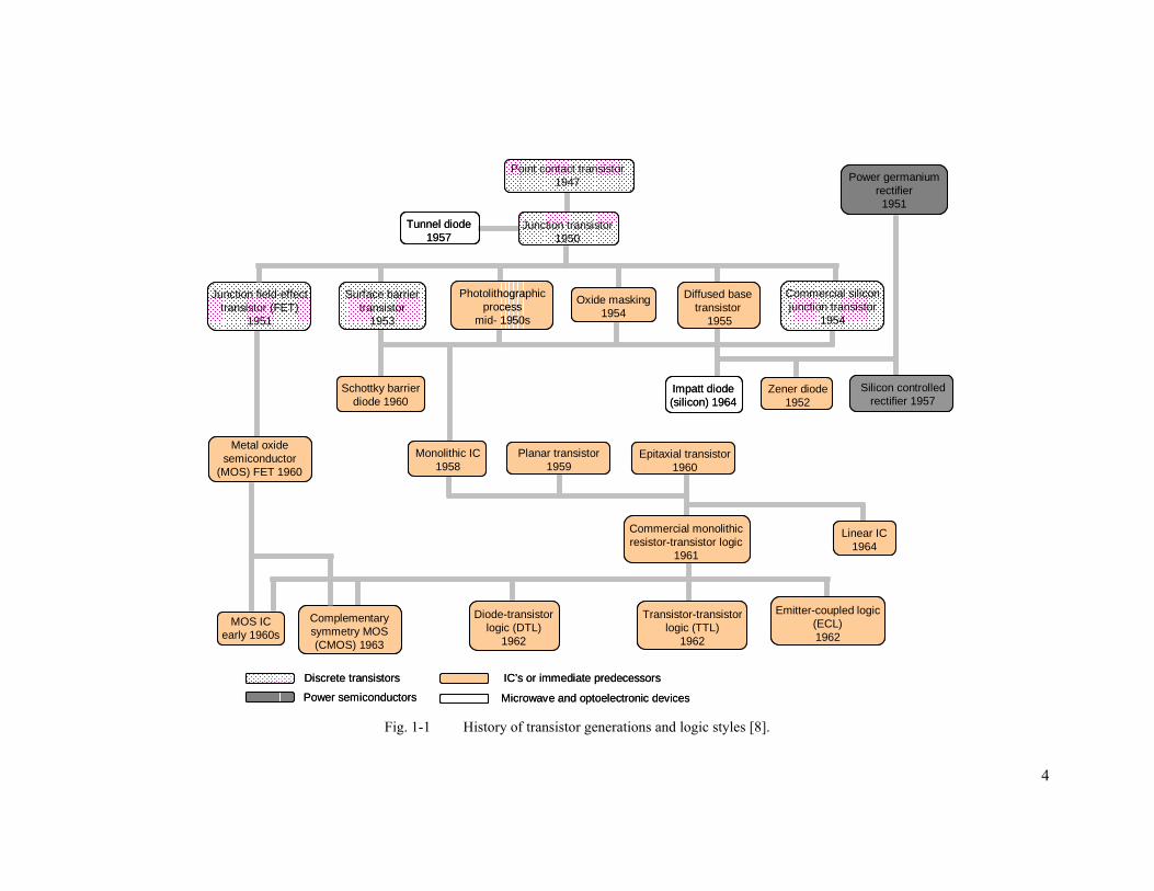
control systems, military, medicine, and a host of other areas. A timeline of these inventions is
shown in Fig. 1-1. These transistors were discrete components connected together with traces of
metal which implemented different circuit functions. Although these innovative devices could
perform better and more reliably at greater frequencies than vacuum tubes or other electro-
mechanical equipment, a system that exclusively consisted of discrete components would be of
limited performance and could not exploit the full potential of semiconductor devices. Not until
the development of the planar process in 1960 which resulted in the familiar integrated circuit, as
shown in Fig. 1-2, could the capabilities of the transistor begin to be fully utilized [7]. This
achievement reinforced the growth of the semiconductor industry, offering a large number of
devices integrated within the silicon, implementing a vast variety of circuit functions.
4
Point contact transistor1947
Junction transistor1950
Junction field-effect transistor (FET)
1951
Surface barrier transistor
1953
Photolithographic process
mid- 1950s
Oxide masking 1954
Diffused base transistor
1955
Power germanium rectifier1951
Schottky barrier diode 1960
Impatt diode (silicon) 1964
Zener diode 1952
Silicon controlled rectifier 1957
Metal oxide semiconductor
(MOS) FET 1960
Monolithic IC 1958
Planar transistor 1959
Epitaxial transistor 1960
Commercial monolithic resistor-transistor logic
1961
MOS IC early 1960s
Complementary symmetry MOS (CMOS) 1963
Diode-transistor logic (DTL)
1962
Transistor-transistor logic (TTL)
1962
Emitter-coupled logic (ECL) 1962
Linear IC1964
Tunnel diode 1957
Commercial silicon junction transistor
1954
Discrete transistors
Power semiconductors
IC’s or immediate predecessors
Microwave and optoelectronic devices
Point contact transistor1947
Junction transistor1950
Junction field-effect transistor (FET)
1951
Surface barrier transistor
1953
Photolithographic process
mid- 1950s
Oxide masking 1954
Diffused base transistor
1955
Power germanium rectifier1951
Schottky barrier diode 1960
Impatt diode (silicon) 1964
Zener diode 1952
Silicon controlled rectifier 1957
Metal oxide semiconductor
(MOS) FET 1960
Monolithic IC 1958
Planar transistor 1959
Epitaxial transistor 1960
Commercial monolithic resistor-transistor logic
1961
MOS IC early 1960s
Complementary symmetry MOS (CMOS) 1963
Diode-transistor logic (DTL)
1962
Transistor-transistor logic (TTL)
1962
Emitter-coupled logic (ECL) 1962
Linear IC1964
Tunnel diode 1957
Commercial silicon junction transistor
1954
Discrete transistors
Power semiconductors
IC’s or immediate predecessors
Microwave and optoelectronic devices Fig. 1-1 History of transistor generations and logic styles [8].

5
Later improvements in the fabrication process and integration on inexpensive silicon resulted
in integrated circuits (IC) with higher yield and hence lower cost, greater performance, and
enhanced reliability. Within the next decade, several logic style families such as transistor-
transistor logic (TTL), emitter-coupled logic (ECL), and complementary metal oxide
semiconductor (CMOS) were proposed. As the complexity of the ICs increased, a profound need
developed for circuits suitable for generalized applications. Indeed, thus far, each IC was
designed to serve a single application, requiring companies to design a variety of low cost
components to maintain profitability. The answer to this profound need was provided by M. E.
Hoff Jr., an engineer at Intel. He envisioned a more flexible way to utilize the capabilities of these
integrated circuits. Encouraged by the founders of Intel, Moore and Noyce, the result of this effort
was the first microprocessor, namely the 4004, which is illustrated in Fig. 1-3. This 0.11 × 0.15
square inch IC could execute addition and multiplication with four-bit numbers, while a bank of
registers was used for storage purposes. Although this capability seems trivial today, the 4004
microprocessor fundamentally altered the way that computers were perceived and used.
Fig. 1-2 The first planar integrated circuit [9].
Since the 4004 was announced in 1971, microprocessors and ICs in general have steadily
improved, demonstrating higher performance and reliability. This fascinating trajectory was
essentially driven by the maturation of the semiconductor manufacturing process, supported by

6
the continued scaling of the transistors. The merits of this evolution were foreseen quite early by
Moore and Noyce, as discussed in the following section, where the physical limitations of
technology scaling are also described.
Fig. 1-3 The 4004 Intel microprocessor [9].
1.2. Interconnects; an old Friend
During the infancy of the semiconductor industry, the connections among the active devices of a
circuit presented an important obstacle for increasing circuit performance. The significant
capacitance of the interconnects necessitated large power drivers and hindered a rapid increase in
performance that could be achieved by the transistors. Noyce had already noticed the importance
of the interconnects, such as the increase in delay and noise due to coupling with neighboring
interconnects [10]. The invention of the integrated circuit considerably alleviated these early
interconnect related problems by bringing the interconnects on-chip. The interconnect length was
significantly reduced, decreasing the delay and power consumption while reducing the overall
cost. From a performance point of view, the delay of the transistors dominated the overall delay
characteristics. Over the next three decades, on-chip interconnects were not the major focus of the
IC design process, as performance improvements reaped from scaling the devices were much
greater than any degradation caused by the interconnects.

7
With continuous technology scaling, however, the interconnect delay, noise, and power grew in
importance [11], [12]. A variety of methodologies at the architectural, circuit, and material levels
have been developed to address these interconnect design objectives. At the material level,
manufacturing innovations such as the introduction of copper interconnects and low-k dielectric
materials helped to prolong the improvements in performance gained from scaling [13]-[17]. This
situation is due to the lower resistivity of the copper as compared to aluminum interconnects and
the lower dielectric permitivity of the new insulator materials as compared to silicon dioxide.
Multi-tier interconnect architectures [18], [19], shielding [20], wire sizing [21], [22], and
repeater insertion [23] are only a handful of the many methods employed to cope with
interconnect issues at the circuit level. Multi-tier interconnect architectures, for example, support
tiers of metal layers with different cross-sections [19], as illustrated in Fig. 1-4. Each tier typically
consists of multiple metal layers routed in orthogonal directions and with the same cross-section.
The key idea of this structure is to utilize wires of decreasing resistance to connect those circuits
located farther away. Thus, the farther the distance among the circuits, the thicker the wires used
to connect these circuits. The increase in the cross-section of the wires is shown in Fig. 1-4. The
thickness of the tiers, however, is limited by the fabrication technology and related reliability and
yield concerns.
Local
Semi-global
Global
Fig. 1-4 Interconnect architecture including local, semi-global, and global tiers. The metal layers on
each tier are of different thickness.

8
Varying the width of the wires, also known as wiring sizing, is another means to manage the
interconnect characteristics. Wider wires lower the interconnect resistance, decreasing the
attenuative behavior of the wire. Although wire sizing typically has an adverse effect on the
power consumed by the interconnect, proper sizing techniques can also decrease the power
consumption [22], [24].
Other practices do not modify the physical characteristics of the propagation medium. Rather,
by introducing additional circuitry and wire resources, the performance and noise tolerance of an
interconnect system can be enhanced. For instance, in a manner similar to the use of repeaters in
telephone lines systems, a properly designed interconnect system with buffers (also known as
repeaters) amplifies the attenuated signals, recovering the originally transmitted signal that is
propagated along a line. Repeater insertion effectively converts the square dependence of the
delay on the interconnect length to a linear function of length, as shown in Fig. 1-5.
τ ~ l2
l
τ ~ l
Fig. 1-5 Repeaters are inserted at specific distances to improve the interconnect delay.
Shielding is an effective technique to reduce crosstalk among adjacent interconnects. Single- or
double-sided shielding, as depicted in Fig. 1-6, is commonly utilized to improve signal integrity.
Shields can also improve interconnect delay and power, particularly in buss architectures, in
addition to mitigating noise. Careful tuning of the relative delay of the propagated signals [25]
and signal encoding schemes [26] are other strategies to maintain signal integrity. Despite the

9
benefits of these techniques, issues arise such as the increase in power consumption, greater
routing congestion, the reduction of wiring resources, and an increase in area.
At higher abstraction levels, pipelining the global interconnects and employing error correction
mechanisms can partially improve the performance and fault tolerance of the wires. The related
cost of these architecture level techniques in terms of area and design complexity, however,
increases considerably. Other interconnect schemes such as current mode signaling [27], wave
pipelined interconnects [28], and low swing signaling [29] have been proposed as possible
solutions to the impeding interconnect bottleneck. These incremental methods, however, have
limited ability to reduce the length of the wire, which is the primary cause of the deleterious
behavior of the interconnect.
(a) (b)
Fig. 1-6 Interconnect shielding to improve signal integrity, (a) single-sided and (b) double-sided
shielding. The shield and signal lines are illustrated by the grey and white color, respectively.
Novel design paradigms are therefore required that do not impede the well established and
historic improvement in performance in next generation integrated circuits. Canonical
interconnect structures that utilize internet-like packet switching for data transfer [30], optical
interconnects [31], and three-dimensional integration are possible solutions for providing
communication among devices or functional blocks within an IC.
On-chip networks can considerably enhance the communication bandwidth among the
individual functional blocks of an integrated system, since each of these blocks utilizes the

10
resources of the network. In addition, noise issues are easier to manage as the layered structure of
the communication protocols utilized within on-chip networks provide error correction. The
speed and power consumed by these networks, however, are eventually limited by the delay of
the wires connecting the network links.
Alternatively, on-chip optical interconnects can greatly improve the speed and power
characteristics of interconnects within an integrated circuit, replacing the critical electrical nets
with optical links [32], [33]. On-chip optical interconnects, however, remain a technologically
challenging problem. Indeed, integrating a modulator and detector onto the silicon within a
standard CMOS process is a difficult task [31]. In addition, the detector and modulator should
exhibit performance characteristics that ensure the optical links outperform the electrical
interconnects [33]. Furthermore, an on-chip optical link consumes larger area as compared to a
single electrical interconnect line. To limit the area consumed by the optical interconnect,
multiplexing of the optical signals (wavelength division multiplexing (WDM)) can be exploited.
On-chip WDM, however, imposes significant challenges.
Volumetric integration by exploiting the third dimension greatly improves the interconnect
performance characteristics of modern integrated circuits while the interconnect bandwidth is not
degraded. In general, three-dimensional integration should not be seen as competitive but rather
synergistic with on-chip networks and optical interconnections. The unique opportunities that
three-dimensional integration offers to the circuit design process and the challenges that arise
from the increasing complexity of these systems are discussed in the following section.
1.3. Three-Dimensional or Vertical Integration
Successful fabrication of vertically integrated devices dates back to the early 80’s [34]. The
structures include 3-D CMOS inverters where the PMOS and NMOS transistors share the same

11
gate, considerably reducing the total area of the inverter, as illustrated in Fig. 1-7. The term
JMOS was used for these structures to describe the joint use of a single gate for both devices [35].
In the following years, research on three-dimensional integration remained an area of limited
scientific interest. Due to the increasing importance of the interconnect and the demand for
greater functionality on a single substrate, vertical integration has recently become a more
prominent research topic. Over the last five years, three-dimensional integration has evolved into
a design paradigm manifested at several abstraction levels, such as the package, die, and wafer
levels. Alternatively, different manufacturing processes and interconnect schemes have been
proposed for each of these abstraction levels [36]. The salient features and important challenges
for three-dimensional systems are briefly reviewed in the following subsections.
n+ n+
p+ p+
n-type
Laser recrystallised CVD polysilicon
Gate oxide for top level device
Joint gate
Gate oxide for bottom level device
Al contacts
n+ n+
p+ p+
n-type
n+ n+
p+ p+
n-type
Laser recrystallised CVD polysilicon
Gate oxide for top level device
Joint gate
Gate oxide for bottom level device
Al contacts
Fig. 1-7 Cross-section of a JMOS inverter [35].
1.3.1. Opportunities for Three-Dimensional Integration
The quintessence of three-dimensional integration is the drastic decrease in the length of the
longest interconnects across an integrated circuit. To illustrate this situation, consider the simple
example structure shown in Fig. 1-8. A common metric to characterize the longest interconnect is
to assume that the length of a long interconnect is equal to twice the length of the die edge.

12
Consequently, assuming a planar integrated circuit with an area A, the longest interconnect in a
planar IC has a length AL D 22max, =− . Implementing the same circuitry onto two bonded dies
requires an area A/2 for each plane while the total area of the system remains the same. Hence,
the length of the longest interconnect for a two plane 3-D IC is .2/23max, AL D =− Increasing the
number of dies within a 3-D IC to four, the area of each die can be further reduced to A/4, and the
longest interconnect would have a length of 4/23max, AL D =− . Consequently, the wire length
exhibits a reduction proportional to n , where n is the number of dies or physical planes that can
be integrated into a 3-D system. Although in this simplistic example the effect of the connections
among circuits located on different dies is not considered, a priori accurate interconnect
prediction models adapted for 3-D ICs also demonstrate a similar trend caused by the reduction in
wire length [37]. This considerable decrease in length is a promising solution for increasing the
speed while reducing the power dissipated by an IC.
2/AA
A 2/A
4/A4/A
AL D 22max, =−
AArea = AAArea =⋅=2
2/2 AAArea =⋅=2
4/4
AL D 23max, =−AL D =−3max,
2/AA
A 2/A
4/A4/A
4/A4/A
AL D 22max, =−
AArea = AAArea =⋅=2
2/2 AAArea =⋅=2
4/4
AL D 23max, =−AL D =−3max,
Fig. 1-8 Reduction in wire length where the original 2-D circuit is implemented in two and four
planes.
Another characteristic of 3-D ICs of greater importance than the decrease in the interconnect
length is the ability of these systems to include disparate technologies. This defining feature of 3-
D ICs offers unique opportunities for highly heterogeneous and multi-functional systems. A real-
time image processing system where the image sensor on the topmost plane captures the light, the

13
analog circuitry on the plane below converts the signal to digital data, and the remaining two
planes of digital logic process the information from the upper planes is a powerful example of a
heterogeneous 3-D system-on-chip (SoC), with considerably improved performance as compared
to a planar implementation of the same system [38], [39]. Another example where the topmost
plane can include other types of sensors such as seismic and acoustic sensors and an additional
plane with wireless communications circuitry is schematically illustrated in Fig. 1-9. A vast pool
of applications, in the military, medical, and wireless communication domains, as well as low
cost consumer products exists for vertical integration, as the proximity of the system components
due to the third dimension is suitable for either the high performance or low power ends of the
SoC application spectrum.
SubstrateHeat Sink
I/O Pad Array
Sensors Antenna
Fig. 1-9 An example of a heterogeneous 3-D system-on-chip comprising sensor and processing planes.

14
1.3.2. Challenges for Three-Dimensional Integration
Developing a design flow for 3-D ICs is a complicated task with many ramifications. A number
of challenges at each step of the design process have to be met for 3-D ICs to successfully evolve
into a mainstream technology. Design methodologies at the front end and mature manufacturing
processes at the back end are required to effectively provide large scale 3-D systems. Several of
the primary challenges to the successful development of 3-D systems are summarized below.
Technological/Manufacturing Limitations
Some of the fabrication issues encountered in the development of 3-D systems concern the
reliable lamination of several ICs, possibly from dissimilar technologies. The stacking process
should not degrade the performance of the individual planes, while guaranteeing the planes
remain bonded throughout the lifetime of the 3-D system. Furthermore, packaging solutions that
accommodate these complicated 3-D structures need to be developed. In addition, the expected
reduction in wirelength depends upon the vertical interconnects utilized to propagate signals and
power throughout the planes of a 3-D system.
The technology of the interplane interconnects is a primary determining factor in circuit
performance. Consequently, providing high quality and highly dense vertical interconnects is of
fundamental importance in 3-D circuits; otherwise, the performance or power gains achieved by
the third dimension will diminish [40]. Alternatively, the density of this type of interconnect
dictates the granularity at which the planes of the system can be interconnected, directly affecting
the bandwidth of the interplane communication.
Testing
Manufacturing a 3-D system typically includes bonding multiple physical planes. The stacking
process can occur either in a wafer-to-wafer or die-to-wafer manner. Consequently, novel testing

15
methodologies at the wafer and die level are required. Developing testing methodologies for
wafer level integration is significantly more complicated than die level testing techniques. The
considerable reduction in turnaround time due to the higher integration, however, may justify the
additional complexity of these testing methods.
An important distinction between 2- and 3-D IC testing is that in the latter case only part of the
functionality of the system is tested at a given time (typically, only one plane is tested at a time).
This characteristic requires additional resources, for example, scan registers embedded within
each plane. Furthermore, additional interconnect resources, such as power/ground pads, are
necessary. These extra pads supply power to the plane during testing. In general, testing strategies
for 3-D systems should not only include methodologies for generating appropriate input patterns
for each plane of the system, but also minimize the circuitry dedicated to efficiently test each
plane within a 3-D stack.
Interconnect Design
Design-for-test strategies are only a portion of the many design methodologies that need to be
developed for 3-D ICs. Interconnect design and analysis of 3-D circuits are also challenging
tasks. This capability is primarily due to the inherent heterogeneity of these systems, where
different fabrication processes or disparate technologies are combined into a 3-D circuit.
Consequently, models that consider the particular traits of 3-D ICs are necessary. In these diverse
systems, global interconnect, such as clock and power distribution, grow in importance.
Furthermore, well developed noise mitigation techniques may not be suitable for 3-D circuits.
Noise caused by capacitive and inductive coupling of the interconnections between adjacent
planes needs to be considered from a 3-D perspective [41]. For example, signal switching on the
topmost metal layer of a digital plane can produce a noise spike in an adjacent analog plane
bonded in a front-to-front fashion with the digital plane. Considering the different forms of 3-D
16
integration and the various manufacturing approaches, the development of interconnect design
techniques and methodologies is a primary focus in high performance 3-D systems.
Thermal Issues
A fundamental concern in the design of 3-D circuits is thermal effects. Although the power
consumption of these circuits is expected to decrease due to the considerably shorter
interconnects, the power density will greatly increase since there is a larger number of devices per
unit area as compared to a planar 2-D circuit. As the power density increases, the temperature of
those planes not adjacent to the heat sink of the package will rise, resulting in degraded
performance, or accelerated wear out mechanisms. Exploiting the performance benefits of
vertical integration while mitigating thermal effects is a difficult task. In addition to design
practices, packaging solutions and more effective heat sinks are additional approaches to alleviate
thermal effects.
CAD Algorithms and Tools
Other classic problems in the IC design process, such as partitioning, floorplanning, placement,
and routing, will need to be revisited in an effort to develop efficient solutions that can support
the complexity of three-dimensional systems. To facilitate the front end design process, a
capability for exploratory design is also required. For example, design entry tools that provide a
variety of visualization options can assist the designer in more easily comprehending and
managing the added complexity of these circuits. In addition, as diverse technologies are
combined within a single 3-D system, algorithms that include behavioral models for a larger
variety of components are needed. Furthermore, the computational power of the simulation tools
will need to be significantly extended to ensure that the entire system can be efficiently evaluated.

17
In this dissertation, emerging 3-D technologies and design methodologies are analyzed and
solutions for certain critical problems are discussed. In the next section, an outline of the
dissertation is provided.
1.4. Dissertation Organization
A brief description of the challenges that 3-D integration faces is provided in the previous section.
Several important problems are considered and innovative solutions are presented in this
dissertation. In the next chapter, various forms of vertically integrated systems are discussed.
Different implementations of three-dimensional circuits at the package and die integration levels
are reviewed. Some of these approaches, such as a wire bonded stacked die, have become
commercially available, while others have not yet left the R&D phase. Although vertical
integration of packaged or bare die offers substantial improvements over planar multi-chip
packaging solutions, the increasing number of I/Os hampers potential performance advancements.
This situation is primarily due to manufacturing limitations hindering aggressive scaling of the
off-chip interconnects in order to satisfy future I/O requirements.
Consequently, in the third chapter, emphasis is placed on those technologies that enable 3-D
integration, where the interconnections between the non co-planar circuits are achieved through
the silicon by short vertical vias. These interconnect schemes provide the greatest reduction in
wire length and, therefore, the largest improvement in performance and power consumption.
Specific fabrication processes that have been successfully developed for three-dimensional
circuits are reviewed.
A theoretical analysis of interconnections in 3-D ICs is offered in the fourth chapter. This
investigation is based on a priori interconnect prediction models. These typically stochastic
models are used to estimate the length of the on-chip interconnects. The remaining sections of

18
this chapter apply the interconnect distributions to demonstrate the opportunities and performance
benefits of vertical integration.
The following four chapters focus on issues related to the physical design of 3-D ICs. The
complexity of the 3-D physical design process is discussed in Chapter 5. Several approaches for
classical physical design issues, such as floorplanning, placement, and routing, from a 3-D
perspective, are reviewed. Other important issues, such as the allocation of decoupling
capacitance, are also presented.
In the sixth chapter, physical design techniques for 3-D ICs are extended to thermal design and
management. Modeling and design methodologies of thermal effects are analyzed. Design
techniques that utilize additional interconnect resources to increase the thermal conductivity
within a multi-plane system are emphasized.
Beyond the reduction in wirelength that stems from three-dimensional integration, the delay of
those interconnects connecting circuits located on different physical planes of a 3-D system (i.e.
the interplane interconnects) can be further improved by optimally placing the through silicon
vertical vias. Considering the highly heterogeneous nature of 3-D ICs that results from the non-
uniform impedance characteristics of the interconnect structures, a methodology is described in
Chapter 7 to minimize the delay of the interplane interconnects. An interconnect line that includes
only one through silicon via is initially investigated. The location of the through silicon via that
minimizes the delay of a line is analytically determined. The degradation in delay due to the non-
optimum placement of the 3-D vias is also discussed. In order to incorporate the presence of
physical obstacles, such as logic cells and pre-routed interconnects (for example, segments of the
power and clock distribution networks), the discussion in this chapter proceeds with interconnects
that include more than one through silicon via. An accurate heuristic is described to implement an

19
efficient algorithm for placing the through silicon vias to minimize the overall delay of a multi-
plane interconnect.
By extending the heuristic for two-terminal interconnects, a near-optimal heuristic for multi-
terminal nets in 3-D ICs is described in Chapter 8. Necessary conditions for locating the through
silicon vias are described. An algorithm that exhibits low computational time is also presented.
The improvement in delay that can be achieved by placing the through silicon vias for different
via placement scenarios is investigated. For the special case where the delay of only one branch
of a multi-terminal net is minimized, a simpler optimization procedure is described. Based on this
approach, a second algorithm is presented. Finally, the sensitivity of this methodology to the
interconnect impedance characteristics is demonstrated, depicting a significant dependence of the
delay on the interconnect parameters.
Another promising design paradigm to appease the foreseen interconnect problems is
networks-on-chip (NoC), where information is communicated among circuits within packets in an
internet-like fashion. The synergy between these two design paradigms, namely NoC and 3-D
ICs, can be exploited to significantly improve the performance and decrease the power
consumption of future communication limited systems. Thus, the ninth chapter is dedicated to
topologies that merge vertical integration with on-chip interconnection networks.
As noted earlier, the distribution of the clock signal in a 3-D IC is an important and difficult
task. In Chapter 10, a variety of clock networks, such as H-trees, rings, tree-like networks, and
trunk based networks, are explored in terms of clock skew and power consumption to determine
an effective clock distribution network for 3-D ICs. A prototype test circuit composed of these
networks has been designed and manufactured with the 3-D fabrication process developed at MIT
Lincoln Laboratories. A description of the design process and related experimental results are
also included in the chapter.

20
Research on the design of 3-D ICs has only recently begun to emerge. Many of the challenges
remain unsolved and significant effort is required to provide effective solutions to the issues
encountered in the design of 3-D ICs. The primary conclusions of this dissertation are
summarized in Chapter 11. Further directions for research that will contribute to the maturation of
this exciting solution to next generation multi-functional systems-on-chip are presented in
Chapter 12.

21
Chapter 2. Manufacturing of 3-D Packaged
Systems
With the ongoing demand for greater functionality resulting in polylithic (multiple IC) products,
longer off-chip interconnects plague the performance of microelectronic systems. The advent of
the system-on-chip (SoC) in the mid-90’s primarily addressed the increasing delay of the off-chip
interconnects. By integrating all of the components on a monolithic substrate, the overall speed of
the system is enhanced while the power consumption is decreased. To assimilate disparate
technologies, however, several difficulties must be surmounted to achieve high yield for the
entire system while mitigating the greater noise coupling among the dissimilar blocks within the
system. Additional system requirements for the RF circuitry, passive elements, and discrete
components, such as decoupling capacitors, which are not easily integrated due to performance
degradation or size limitations, have escalated the need for technological innovations. Three-
dimensional or vertical integration and system-on-package (SoP) have been proposed to
overcome many of the inherent SoC constraints. The concepts of vertical integration and SoP are
described in Sections 2.1 and 2.2, respectively, and the commonality between these innovative
paradigms is also discussed. Several three-dimensional technologies for 3-D packaging are
reviewed in Section 2.3. The technological implications of 3-D integration at the package level
are summarized in Section 2.5.
2.1. Three-Dimensional Integration
One of the first initiatives demonstrating three-dimensional circuits was reported in 1981 [34].
This work involved the vertical integration of PMOS and NMOS devices with a single gate to

22
create an inverter, considerably reducing the total area and capacitance of the inverter. A cross-
section of this inverter is illustrated in Fig. 2-1. Several other approaches to three-dimensional
integration, however, have been developed both at the package and circuit level where bare or
packaged die are vertically integrated, permitting a broad variety of interconnection strategies.
Each of these vertical interconnection techniques has different advantages and disadvantages.
Other more esoteric technologies for 3-D circuits have also been proposed. To avoid confusion,
therefore, a crucial differentiation among the various 3-D integration approaches is maintained in
this chapter. Two primary categories of 3-D systems are discerned, namely system-in-package
(SiP) and three-dimensional integrated circuits (3-D IC). The criterion to distinguish between SiP
and 3-D IC is the interconnection technology that provides communication for circuits located on
different planes of a 3-D system. In SiP, through silicon vias (TSV) with high aspect ratios are
typically utilized. Due to the size of these vias, a high vertical interconnect density cannot be
achieved. Hence, these interconnects provide coarse grain connectivity among circuit blocks
located on different planes. Alternatively, in 3-D ICs, fine grain interconnection among devices
on different planes is achieved by narrow and short through silicon vias.
p+ p+
n+ n+
Gate
VDD
Vout
p+ p+
n+ n+
Gate
VDD
Vout
Fig. 2-1 Three-dimensional stacked inverter [34].

23
2.1.1. System-in-Package
A system-in-package is described henceforth as an assemblage of either bare or packaged die
along the third dimension, where the interconnections through the z-axis are primarily
implemented through the following means:
• Wire bonding
• Vertical interconnects along the periphery of the die/package
• Long and wide, low density vertical interconnects (in an array arranged across the
die/package)
• Metallization between the faces of a 3-D stack
Die or package bonding can be implemented by utilizing a diverse collection of materials, such as
epoxy and other polymers. Some examples of SiP structures are illustrated in Fig. 2-2, while each
one of these manufacturing techniques is discussed in Section 2.3.
Bonded wires
Vertical interconnects
Solder balls
Conductors
(a) (b)
(c) (d)
Fig. 2-2 Examples of SiP, (a) wire bonded SiP [42], (b) solder balls at the perimeter of the planes [43],
(c) area array vertical interconnects, and (d) interconnects on the faces of the SiP [44].

24
2.1.2. Three-Dimensional Integrated Circuits
3-D ICs can be conceptualized either as a sequential or a parallel process. In the case of a
sequential process, the devices and metal layers of the upper planes of the stack are grown on top
of the first plane. Hence, the 3-D system can be treated as a monolithic structure. Alternatively, a
3-D IC can be created by bonding multiple wafers or bare die. The distinctive difference between
an SiP and a 3-D IC is the vertical interconnect structure. Communication among different die
within a 3-D IC is implemented by
• High density short and thin through silicon vias (TSV) (placed at any point across the die
not occupied by transistors)
• Capacitive coupling among parallel metal plates located on vertically adjacent die
• Inductive coupling among inductors located on vertically adjacent die
Some characteristic examples of these communication mechanisms for 3-D ICs are illustrated in
Fig. 2-3. Although 3-D ICs can be characterized as a subset of SiP, the advantages of 3-D vertical
interconnects as compared to the interconnect mechanisms utilized in SiP are substantially
greater. In addition, 3-D ICs face fewer performance limitations as compared with the SiP
approach, unleashing the potential of three-dimensional integration. Various technologies for 3-D
ICs are investigated in Chapter 3.

25
1st plane
2nd plane
Through silicon vias (TSV)
(a) (b)
Receiver
ReceiverReceiver
TransmitterTransmitter
(c)
1st plane
2nd plane
Through silicon vias (TSV)
1st plane
2nd plane
Through silicon vias (TSV)
(a) (b)
Receiver
ReceiverReceiver
TransmitterTransmitter
(c) Fig. 2-3 Various communication schemes for 3-D ICs [45], (a) short through silicon vias, (b) inductive
coupling [36], and (c) capacitive coupling [46].
2.2. System-on-Package
As portability has become a fundamental characteristic in many consumer products, systems with
a small footprint, low weight, long battery life, and equipped with a variety of features typically
attract a significant market share. Communications is the most remarkable feature of these
products. Wireless communication, in turn, requires RF circuitry that includes passive
components, such as resistors and high Q inductors that cannot be easily and cost effectively
fabricated on the silicon. In addition, off-chip capacitors of different sizes are required to manage
the voltage droop and simultaneous switching noise at the package level [47].
Implementing all of these components within a package and not as discrete components on a
printed wiring board (PWB) contributes significantly to system miniaturization. System-on-
package (SoP) is a system level concept that includes passive components manufactured as thin

26
films. High performance transceivers and optical interconnects can also be embedded within a
package [48]. State-of-the-art microvia provide communication among the embedded circuits and
the mounted sub-systems [49]. Microvias are vertical interconnects that connect the various
components of an SoP through the laminated layers of the SoP substrate. Consequently, SoP
supports wiring among the various sub-systems as in an SiP, and can also contain system
components integrated in the package.
A wide spectrum of sub-systems that gather, process, and transmit data can be included in an
SoP. Sensors and electromechanical devices that record environmental variables, analog circuits
that process and convert the analog signals to digital data, digital circuits, such as ASICs, DSP
blocks, and microprocessors, memory modules, and RF circuits that provide wireless
communication, is a short and not exhaustive list of components that can be mounted on an SoP.
Some of these sub-systems can be vertically integrated, making an SoP a hybrid technology that
combines planar ICs and 3-D circuits, as illustrated in Fig. 2-4a. The set of functions that can be
implemented by an SoP, SiP, 3-D IC, and SoC are qualitatively represented in Fig. 2-4b. As
expected, since an SoP is a system integrating technology, an SoP can simultaneously include an
SiP, 3-D IC, and SoC, providing significant functionality. An SiP is typically used in those
applications that include memory modules and microprocessors or ASICs. 3-D ICs are currently
more limited than an SiP (shown as a subset of an SiP in Fig. 2-4b). Finally, SoCs can be
manifested both as a planar system in an SoP and a three-dimensional component as an SiP or 3-
D IC.
Several manufacturing and design challenges, as illustrated in Fig. 2-5, need to be
circumvented to ensure that the various forms of three-dimensional integration can be
economically produced. From a technology perspective, a 3-D system should exhibit yield similar
to a 2-D circuit. Since each plane within a stack can be separately prepared with a high yield

27
process, the primary challenge is to guarantee a high yield bonding process. The bonding process
should ensure reliable interconnectivity of circuits located on different planes. In addition, the
fabrication process of the vertical vias is a critical component contributing to the total system
yield. Finally, advanced packaging technologies provide highly efficient heat transfer from the 3-
D system to the ambient environment.
RF IC Analog/Digital ICOpto ElecµP
Memory
Memory
Passive components
Decoupling capacitorsRF, Filters
SiP
SoP
SoC
SoP
SiP
3-D IC
SoC
(a) (b)
RF IC Analog/Digital ICOpto ElecµP
Memory
Memory
Passive components
Decoupling capacitorsRF, Filters
SiP
SoP
SoCRF IC Analog/Digital ICOpto ElecOpto Elec
µP
Memory
Memory
Passive components
Decoupling capacitorsRF, Filters
SiP
SoP
SoC
SoP
SiP
3-D IC
SoCSoP
SiP
3-D IC
SoC
(a) (b) Fig. 2-4 (a) A typical SoP [48] and (b) relation of SoP, SiP, 3-D IC, and SoC.
Overcoming these manufacturing challenges results in improved SiP systems where reliable
interconnect mechanisms that are more efficient than wire-bonding can be employed, improving
the performance of this form of three-dimensional integration. The potential of vertical
integration, however, can be best exploited if various design challenges, as shown in Fig. 2-5, are
also met, resulting in general purpose 3-D circuits. Design methodologies for 3-D circuits,
however, barely exist. In addition, thermal management techniques for these high density circuits
are extremely important. The development of specific CAD tools integrated into a design flow
that can support the complexity of three dimensions is therefore an imperative need.
Mitigating these manufacturing and design issues will greatly promote the evolution of 3-D
ICs, considerably expanding the application pool for this important manifestation of vertical
integration. These technological developments will establish 3-D ICs as the primary
representative of three-dimensional integration. Otherwise, vertical integration will primarily
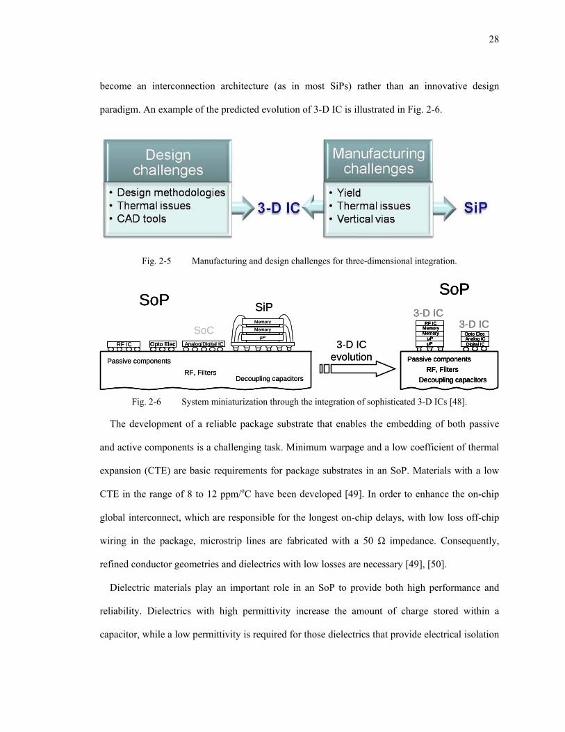
28
become an interconnection architecture (as in most SiPs) rather than an innovative design
paradigm. An example of the predicted evolution of 3-D IC is illustrated in Fig. 2-6.
Fig. 2-5 Manufacturing and design challenges for three-dimensional integration.
RF IC Analog/Digital ICOpto ElecµP
Memory
Memory
Passive components
Decoupling capacitorsRF, Filters
SiPSoP
SoC
Passive components
Decoupling capacitorsRF, Filters
µPMemoryMemory
µP
RF IC
Digital ICAnalog ICOpto Elec
SoP3-D IC
3-D IC
3-D IC evolution
RF IC Analog/Digital ICOpto ElecOpto ElecµP
Memory
Memory
Passive components
Decoupling capacitorsRF, Filters
SiPSoP
SoC
Passive components
Decoupling capacitorsRF, Filters
µPMemoryMemory
µP
RF IC
Digital ICAnalog ICOpto Elec
SoP3-D IC
3-D IC
Passive components
Decoupling capacitorsRF, Filters
µPMemoryMemory
µP
RF IC
Digital ICAnalog ICOpto Elec
Passive components
Decoupling capacitorsRF, Filters
µPMemoryMemory
µP
RF IC
Digital ICAnalog ICOpto Elec
SoP3-D IC
3-D IC
3-D IC evolution
Fig. 2-6 System miniaturization through the integration of sophisticated 3-D ICs [48].
The development of a reliable package substrate that enables the embedding of both passive
and active components is a challenging task. Minimum warpage and a low coefficient of thermal
expansion (CTE) are basic requirements for package substrates in an SoP. Materials with a low
CTE in the range of 8 to 12 ppm/oC have been developed [49]. In order to enhance the on-chip
global interconnect, which are responsible for the longest on-chip delays, with low loss off-chip
wiring in the package, microstrip lines are fabricated with a 50 Ω impedance. Consequently,
refined conductor geometries and dielectrics with low losses are necessary [49], [50].
Dielectric materials play an important role in an SoP to provide both high performance and
reliability. Dielectrics with high permittivity increase the amount of charge stored within a
capacitor, while a low permittivity is required for those dielectrics that provide electrical isolation

29
among neighboring interconnects, thereby reducing the coupling capacitance. A metric
characterizing the loss of a dielectric material is the loss tangent (tan δ). This metric describes the
ratio of the energy dissipated by the capacitor formed between the conductors and the energy
stored in the capacitor. Low tangent loss for achieving low latency signal transmission and high
modulus for minimum warpage across the package is desirable. In addition, dielectrics should
exhibit excellent adhesion properties to avoid delamination and withstand, without any
degradation in material properties, the highest temperature used to manufacture the package.
Some of the dielectric materials that have been developed for SoP with the relevant material
properties are listed in Table 2-1.
TABLE 2-1 HIGH PERFORMANCE DIELECTRIC MATERIALS [49].
Dielectric material Dielectric constant Loss tangent @ 1GHz Modulus GPa X,Y, CTE ppm/oC Polyimide 2.9-3.5 0.002 9.8 3-20
BCB 2.9 <0.001 2.9 45-52 LCP 2.8 0.002 2.25 17 PPE 2.9 0.005 3.4 16
Poly-norbornene 2.6 0.001 0.5-1 83 Epoxy 3.5-4.0 0.02-0.03 1-5 40-70
2.3. Technologies for System-in-Package
A system-in-package constitutes a significant and widely commercialized variant of vertical
integration. The driving force towards SiP is the increase in packaging efficiency, which is
characterized by the die to package area ratio, the reduced package footprint, and the decreased
weight. Homogeneous systems consisting of multiple memory dies and heterogeneous stacks
including combinations of memory modules and an ASIC or a microprocessor are the most
common type of SiP, which has been commercialized by several companies [44], [51]. The
typical communication mechanism among different planes of the stack is realized through wire
bonding, as discussed in the following subsection.

30
2.3.1. Wire Bonded System-in-Package
Wire bonding for a system-in-package is a commonplace technique. Due to the simplicity of the
process, the required time to fabricate such an SiP is substantially shorter as compared to the
turnaround time for an SiP that utilizes other interconnect techniques. Various wire bonded SiP
structures are depicted in Fig. 2-7. The parameters that determine the packaging efficiency of
these structures are the thickness of the bonded die and spacers, thickness of the adhesive
materials, capability of providing multiple rows of wire bonding, and the size of the bumps used
to mount the bottom die of the stack onto the package substrate. Alternatively, the performance of
the stack is determined from the length of the bonding wires and the related parasitic impedances.
Communication among the die of the SiP is primarily achieved through the package substrate
and, as shown in Fig. 2-7c, through wire bonding from one IC substrate to another IC substrate.
Multi-row wiring
Adhesive
SpacerDie to die
wire bondingDie to packagewire bonding
(a) (b) (c)
(d)
Multi-row wiring
Adhesive
Multi-row wiring
Adhesive
SpacerSpacerDie to die
wire bondingDie to packagewire bonding
Die to diewire bonding
Die to packagewire bonding
(a) (b) (c)
(d) Fig. 2-7 Wire bonded SiP, (a) dissimilar dies with multiple row bonding, (b) wire bonded stack
delimited by spacer, (c) SiP with die-to-die and die-to-package wire bonding, and (d) top view of wire
bonded SiP [42].

31
The manufacturing process for the structures shown in Fig. 2-7 comprises the following key
steps. All of the stacked dies or wafers are thinned with grinding and polished to a thickness of 50
µm to 75 µm [42]. Although aggressive wafer thinning is desirable, the die or wafer must be of
sufficient thickness to avoid curling and cracking during the bonding process. The length of the
bonding wires or, equivalently, the loop overhang also depends upon the thickness of the attached
wafers. In Table 2-2, the overhang requirement as a function of the die thickness is reported.
TABLE 2-2 LOOP OVERHANG REQUIREMENTS VS. DIE THICKNESS [42].
Die thickness [µm] Overhang [mm] 100 2.0 75 1.0 63 0.7
The bottom die of the stack is bumped and mounted in a flip chip manner onto the package
substrate. The remaining die are successively adhered to the stack through thin film epoxies. In
certain cases, spacers between subsequent die are required. These spacers provide the necessary
clearance for the bonding wire loop. Epoxy pastes and other thick film materials are utilized with
a thickness ranging from 100 µm to 250 µm [42]. A uniform gap between the attached die is
required across the area of the spacer and, therefore, spheres of spacer material can be utilized for
this purpose. With these spacers, similar die or dies with quite diverse areas can be stacked on an
SiP.
A wire bonded SiP including up to four or five dies have been demonstrated [42], while two
die stacking is quite common [52]. Increasing the number of die on an SiP is hampered by the
parasitic impedance of the bonding wires and the available interconnect resources. For example,
bonding wires can exhibit an inductance of a few nH. Consequently, a low loop profile is required
to control the impedance characteristics of the wire. Additionally, multiple rows for bonding can
be utilized to increase the interconnect bandwidth. For multiple row wiring, low height bonding
wires are also necessary. The wire pitch for three bonding rows is listed in Table 2-3. Although

32
the off-chip interconnects are decreased with wire bonding, limitations due to parasitic
interconnect impedances and constraints on the number of die that can be wire bonded have led to
other SiP approaches that provide greater packaging efficiency while exhibiting higher
performance. These improved characteristics are enabled by replacing the bonding wires with
shorter through-hole vias or solder balls [52]. This SiP technique is discussed in the following
subsection.
TABLE 2-3 REQUIRED BONDING WIRE PITCH FOR MULTIPLE ROW BONDING [42].
Row no. Wirebond pitch [µm] 1 40 2 25/50 3 20/60
2.3.2. Peripheral Vertical Interconnects
To overcome the constraints of wire bonding, SiPs are implemented with peripheral interconnects
formed with solder balls and through-hole vias. Several approaches based on this type of
interconnect have been developed, some of which are illustrated in Fig. 2-8 [44]. A greater
number of die can be integrated with this approach as the constraints due to the wire parasitic
impedance and the length are considerably relaxed. An interconnect structure utilized to provide a
reduced pitch connection between the die and the package, known as an interposer, is included in
each plane of an SiP, as shown in Fig. 2-8. The interposer also provides the wiring between the
die and the solder balls or through-hole vias at the periphery of the system. Several companies
have developed similar SiP technologies. Micron Corporation uses the method shown in Fig. 2-8b
to produce high density SRAM and DRAM memory chips [53]. In another technique developed
by Hitachi, vertical pillars are attached onto the PCB, called “PCB frames,” to accommodate the
vertical interconnects [54]. The I/Os of the IC are transferred through tape adhesive bonding
(TAB) to the PCB frames, as illustrated in Fig. 2-8c. High density memory systems also use this
method.

33
The basic steps of a typical process for SiP with peripheral interconnects are depicted in Fig.
2-9 [43]. Initially, bumps are deposited on the interposers, while solder-plated polymer spheres
are attached on the periphery of the interposers and provide the communication among the dies of
the stack. Next, the IC is attached to the interposer employing a flip chip technology. Vertical
stacking of the interposers through the solder balls follows. The solder balls constitute an
important element of the stacking process as these joints provide both the electrical connections
as well as the mechanical support for the SiP. In addition, the height of the solder ball core
provides the necessary space between successive interposers where the die is embedded. Solder
balls with a height greater than 200 µm can therefore be utilized. If the solder balls collapse, the
reliability of an SiP can be severely affected. Finally, in order to further reinforce the durability of
this SiP structure, an epoxy underfill between adjacent interposers is applied. A similar technique
has been developed by IMEC where the 3-D stack is achieved by direct soldering two contiguous
solder balls (“ball on ball” bonding) [55].
Solder ballsDie
Die
Via
Spacer
Ceramic
(a) (b)PCB frame
Die
Die
Die
PCB
(c)
Solder ballsSolder ballsDie
Die
Via
Spacer
Ceramic
Die
Die
Via
Spacer
Ceramic
(a) (b)PCB frame
Die
Die
Die
PCB
(c) Fig. 2-8 SiP with peripheral connections, (a) solder balls [43], (b) through-hole via and spacers [53],
and (c) through-hole via in a PCB frame structure [54].

34
Further enhancements of this bonding technique results in a decreased diameter of the vertical
interconnects by utilizing through-hole electrodes and bumps with a diameter and depth ranging
from 20 µm to 30 µm and 30 µm to 50 µm, respectively [56]. The through-hole electrodes are
etched and gold (Au) bumps are grown on the front and back side of the interposers to bond the
IC. An important characteristic of this method is that only low temperatures are used to compress
the stack. In addition, the thickness of the interposers is smaller than 50 µm, permitting greater
packaging efficiency. The expected height of a ten plane SiP implemented with this method is
approximately 1 mm, a significant reduction in height over wire bonding techniques.
Fig. 2-9 Basic manufacturing phases of an SiP, (a) interposer bumping and solder ball deposition, (b)
die attachment, (c) plane stacking, and (d) epoxy underfill for enhanced reliability.
Although through-hole vias yield higher packaging efficiency and mitigate certain performance
issues related to wire bonding, a higher density vertical interconnect is required as interconnect
demands increase. Indeed, with peripheral interconnects, the wire pitch decreases linearly with
the number of interconnects. Alternatively, providing interconnects arranged as an array across
the die of an SiP greatly increases wiring resources, while the interconnect pitch decreases with
the square root of the number of interconnects [52].

35
2.3.3. Area Array Vertical Interconnects
An SiP with peripheral interconnects are inherently limited by the interconnect density and the
number of components that can be integrated within a stack. Area array vertical interconnects
improve the interconnect density among the planes of a 3-D system, offering opportunities for
greater integration. Solder bumps or through-hole vias can be utilized for the area array
interconnects; however, the processing steps for these two types of interconnects differ
considerably.
In a manufacturing process developed by IBM and Irvine Sensors, the memory chips are
bonded together to produce a 3-D silicon cube [57], [58]. The wafers are processed in order to
interconnect the I/O pads of the die to the bumps on the face of the cube. This metallurgical step
is followed by wafer thinning, dicing, and die lamination to create the silicon cube. The stacking
process is achieved through controlled thermocompression. An array of controlled collapse chip
connect (C4) bumps provides communication among the planes of the cube. The interconnect
density achieved with this technology is 1400 C4 bumps, consuming an area of 260 mm2. Note
that with this technique, all of the planes within the cube share a common C4 bump array.
A higher contact density has recently been developed by 3D-PLUS and THALES [59]. A
heterogeneous wafer is formed by attaching the individual ICs onto an adhesive tape that provides
mechanical support. The I/O pads from each IC are redistributed with two different techniques
into coarser pads whose size depends upon the alignment accuracy prior to stacking the ICs. The
first technique for pad redistribution utilizes two layers of copper embedded in benzocyclobutene
(BCB). The average measured contact resistance is ~ 2 Ω. Another technique for developing the
vertical interconnects between the planes includes laminated films (as a dielectric) and copper.
Despite the large number of steps, test vehicles have shown no signs of delamination among the
adhered planes within the SiP.
36
Prior to bonding, the wafer thickness is reduced to 150 µm with grinding and mechanical
polishing. Once the target thickness is achieved, the wafer is diced and tested for IC failures or
open contacts during connection of the die I/Os with the coarser pads of the package. Only known
good die (KGD) are therefore bonded, guaranteeing high yield. The 3-D system is connected
through liquid adhesive and compression. The resulted SiP can contain up to six ICs with a height
less than a millimeter.
In these two techniques, each plane of the stack is designed and fabricated without any
constraints imposed by the assembly process of the SiP, as the vertical interconnects are
implemented on one face of the plane and not through the plane. Alternatively, the vertical
interconnects are implemented with copper bumps and electrodes formed through the stacked
circuits within the SiP [60]. The stacked die are aggressively thinned to a thickness of 50 µm and
copper (Cu) electrodes with a 20 µm pitch are formed. Square Cu bumps with a sidelength of 12
µm and a height of 5 µm are electroplated and covered with a thin layer of tin (Sn) (< 1 µm) for
improved bonding. The bonding is further enhanced by a non-conductive particle paste (NCP),
which is also used to encapsulate the Cu bumps.
Two bonding scenarios with different temperature profiles have been applied to stack four 50
µm thick dies on a 500 µm interposer [60]. In the first case, a bonding force is applied at high
temperature (245 oC), while in the second scenario, the temperature is reduced to 150 oC
accompanied by a thermal annealing step at 300 oC. Both of these scenarios demonstrate good
adhesion among the die, while the backside warpage is less than 3 µm for a square die with a side
length of 10 mm.
With array structured interconnects, the throughput among the die of the stack can be improved
over an SiP with peripheral interconnect and bonding wires. The solder ball or bump size,
however, constitutes an obstacle for vertically integrated systems with ultra high interconnect

37
density. Another concern is the re-wiring that is necessary in some of these techniques, which
prevents achieving the maximum possible reduction in the length of the interplane interconnects.
2.3.4. Metallizing the Walls of an SiP
Another SiP approach entails several ICs mounted on thin substrates with wiring or stacked PCBs
to yield a 3-D system. Interconnects among the circuits on different dies are implemented through
metal traces on the individual faces of the cube. The interconnect density achieved with this
technique is similar to that of a wire bonded SiP; however, a higher number of monolithic
structures can be integrated within the cube.
One application of this type of SiP is a high density SRAM memory stack manufactured with a
process invented at Irvine Sensors [61]. In this process, each module is separately tested before
the stacking step. In this way, the KGD problem is significantly appeased as the faulty parts can
be excluded or reworked in the initial steps. Fully operational ICs are selected and glued with a
thin layer of adhesive material between each pair of ICs. The bonded stack undergoes a baking
step with a specific curing profile. In order to reveal the buried metal leads from each memory
module, the stack is plasma etched. If required, more than one face of the cube can be etched. The
dimensions of the leads are 1 µm thick and 125 µm wide. The etching step exposes not only the
metal leads but also the substrate of the stacked memory planes. Passivation is required to isolate
the substrates from the metal traces created on the sidewall of the stack. Several layers of
polyimide are deposited, where the thickness of each layer is greater than the exposed metal
leads. Lift-off photolithography and sputter deposition are utilized to create the interconnects,
including the busses, and the pads on the face of the cube with a titanium-tungsten/gold (Ti-
W/Au) alloy. The pads on the sidewall of the cube connected to the metal leads of each IC form a
T-shape interconnect, which is referred to as a “T-connection.” The resistance of a T-connection

38
has been measured to be approximately 25 mΩ [61]. Finally, a soldering step is used to attach the
stack onto a silicon substrate or PCB, permitting the stack to be connected to external circuitry.
Prototypes with as many as seven stacked ICs demonstrate a considerably higher integration as
compared with a wire bonded SiP. These prototypes are diced from an initial stack consisting of
70 identical ICs. Producing shorter stacks from a taller cube contributes to a reduction in the
overall fabrication time. In addition to memory products, an image capturing and processing
system fabricated with a similar technique has been introduced [62], [63]. The entire fabrication
process consists of seven basic steps. Each IC is attached onto laminated films or, if necessary, a
PCB along with discrete passive components. The substrate contains metal tracks, such as copper
lines plated with gold, and the I/Os of the IC are wire bonded to these tracks. Each mounted IC is
tested before bonding. This testing step improves the total yield as bonding the KGD is
guaranteed. Testing includes validation of the interconnections connecting the IC to the laminated
film or PCB. The test structures are placed in a plastic mold and encapsulated with an epoxy
resin. After removal of the mold, a sawing step is applied to expose the metal tracks of each PCB
within the stack. Alternatively, a deeper sawing can be applied to reveal the bonding wires rather
than the metal tracks of the PCB, as shown in Fig. 2-10. The cubical structure is plated with
conventional electroplating techniques. The plated surfaces of the cube are patterned by a laser to
produce the interconnects connecting the planes of the SiP. The typical dimensions for these
sidewall interconnects are six to seven micrometers thick and 500 µm wide. In the last step, the
SiP can be soldered to a PCB on one face of the cube.

39
IC
IC
IC
IC IC
IC
IC
IC
IC
IC
IC
IC
(a) (b) (c)
Epoxy resin
ICIC
ICIC
ICIC
ICIC IC
IC
IC
IC
ICIC
ICIC
ICIC
ICIC
IC
IC
IC
IC
ICIC
ICIC
ICIC
ICIC
(a) (b) (c)
Epoxy resin
Fig. 2-10 Cross-section of the SiP after removing the mold, (a) the SiP encapsulated in epoxy resin, (b)
sawing to expose the metal traces, and (c) sawing to expose the bonding wires [63].
Although the methods used in each step of this technique are well known and relatively low
cost, there are several design and efficiency concerns regarding the reliability of the surface
contacts. These issues include the reliability of the internal contacts of each IC to the external
interconnections on the cube faces, and the thermo-mechanical performance of a dense SiP.
Finally, a particularly long interconnect path may be required to connect two circuits from
different planes within an SiP. Consequently, utilizing thin and short vertical interconnects for
communication among the planes within a 3-D system can result in higher performance. Different
3-D technologies result in dissimilar performance enhancements for an integrated system, while
imposing a specific cost overhead due to the complexity of the fabrication process. A comparison
of the manufacturing cost of the 3-D technologies, discussed in this chapter, is provided in the
following section.
2.4. Cost Issues for 3-D Integrated Systems
Both circuit and packaging performance is considerably enhanced by the third dimension. A
significant increase in speed and decrease in power consumption are the primary improvements in
circuit performance. Additionally, the packaging density is greatly improved by efficiently

40
exploiting the unused volume within the package. Alternatively, the fabrication cost of these
technologies should be considered when selecting the target technology to satisfy the
performance goals of an integrated system.
Two primary components of the manufacturing cost of an integrated circuit are the silicon area
and the number of lithography steps required to fabricate a circuit. In 3-D systems, the footprint
of the system is reduced. Multi-plane structures, however, complicate the manufacturing process,
primarily due to the need to bond the individual planes. The efficiency of the bonding process
therefore directly affects the overall yield and varies according to the 3-D technology and the type
of inter-plane communication, for example, wire bonds or through silicon vias. An analytic model
that characterizes the cost of a 3-D system consisting of n planes is described by [64]
[ ]BWwafer
designn
Bn
W
MnnMAA
YYC )1(1
1 −+= − , (2-1)
where YW and YB are the yield of the process to fabricate each wafer and the yield of each bonding
phase, respectively. Assuming wafer scale integration, Awafer is the wafer area and Adesign is the
maximum footprint of the bonded planes. MW and MB are, respectively, the number of steps to
fabricate each plane/wafer and the steps of the bonding process.
From this model, 3-D technologies decrease the cost of a system by reducing the physical
footprint of the circuit. This improvement however is counterbalanced by the exponential
decrease in the overall yield of the manufacturing process due to the multiple bonding and
lithography steps. This situation suggests that the complexity of the 3-D manufacturing process
can result in significantly higher cost for multi-plane multi-functional systems as compared to a
standard 2-D CMOS process typically used in systems-on-chip. A comparison of a multi-window
display application and a graphics processor based on this model demonstrates that 3-D
technologies produce a moderate increase of 49% and 43%, respectively, in the manufacturing
cost [64]. The significant decrease in wirelength and, consequently, interconnect resources and

41
the increase in the performance, however, justify the choice of a 3-D technology for high
performance applications.
The model of (2-1) is biased towards 2-D systems-on-chip since the manufacturing
implications of combining different types of circuits, such as memory and logic, onto a single die
such as in an SoC are not considered. These yield limitations are removed in 3-D technologies,
since each type of circuit can be placed on an individual plane and fabricated with the appropriate
high yield process. More accurate analytic models that consider these issues suggest that 3-D
technologies can offer economical fabrication of multi-plane systems for high performance
systems [65]. A theoretical comparison of a wireless sensor node and a third generation mobile
terminal implemented with different 3-D technologies is listed in Table 2-4. As listed in this
table, when multiple aspects of a system, such as cost, performance, and temperature, are
considered, 3-D integration can outperform planar systems-on-chip. 3-D integration is therefore
an excellent candidate for high performance and heterogeneous systems. Furthermore, wafer
scale integration of 3-D circuits with high density vertical interconnects exhibits considerably
higher performance as compared to a 3-D system-in-package. This attractive 3-D technology is
discussed in the following chapter.
TABLE 2-4 COST PERFORMANCE COMPARISON OF 3-D TECHNOLOGIES [65].
Parameter Wireless sensor node 3G mobile terminal SoC 2-D SoP 3-D SiP 3-D
wafer to wafer
3-D die to wafer
SoC 2-D SoP 3-D SiP 3-D wafer to
wafer
3-D die to wafer
Normalized area
1.00 3.92 0.78 0.71 0.71 1.00 1.94 0.75 0.71 0.71
Overall yield
0.95 0.98 0.98 0.92 0.94 0.56 0.98 0.98 0.71 0.94
Normalized cost
1.00 4.11 4.04 1.14 2.96 1.00 0.40 0.40 0.38 0.33
Delay [ps] 127.37 176.36 148.33 83.9 83.9 317.88 205.37 168.34 259.63 259.63 ∆T (oC) 39.16 12.39 52.8 312.74 312.74 26.38 14.67 36.9 73.96 73.96

42
2.5. Summary
The technological progress and related issues regarding three-dimensional integration at the
package level can be summarized as follows:
• Three-dimensional packaging includes bare or packaged die vertically integrated using a
variety of interconnection schemes.
• A system-in-package (SiP) and three-dimensional integrated circuits (3-D ICs) are
currently the primary methods used for 3-D systems. A major difference between these
approaches is the type of vertical interconnects used to connect the circuits located on
different planes.
• A system-in-package is an assemblage of either bare or packaged die connected along the
third dimension, where the interconnections through the z-axis are primarily implemented
by wire bonding, metallization on the faces of the 3-D stack, vertical interconnects along
the periphery of the die/package, and low density vertical interconnects arranged as an
array across the die/package.
• These different SiP interconnect structures are sorted in descending order of vertical
interconnect density.
• 3-D ICs are interconnected with high density short and thin TSVs, supporting low level
integration rather than die or package level integration as in an SiP.
• An SoP is a hybrid technology that combines planar ICs and 3-D circuits within a compact
system. The primary difference as compared to an SiP is that an SoP supports more than
wiring, containing system components within the package.
• An SiP has higher packaging efficiency and a smaller footprint and weight as compared to
a conventional 2-D system.
• Wire bonded SiP are limited by the impedance of the bonding wires.

43
• An SiP with peripheral interconnects are implemented by solder balls and through-hole
vias. SiP are inherently limited by the interconnect density as the wire pitch decreases
linearly with the number of interconnects.
• An SiP with array structured interconnects can improve the interconnect density as
compared to an SiP with peripheral interconnects and bonding wires as the interconnect
pitch decreases with the square root of the I/O (or pin) requirements.
• 3-D technologies increase the manufacturing cost of an integrated system. This additional
manufacturing cost, however, is counterbalanced by the decrease in the area, increase in
the die yield, and increase in the performance of the overall system.

44
Chapter 3. 3-D Integrated Circuit Fabrication
Technologies
A system-in-package (SiP) offers a large number of advantages over traditional 2-D SoC, such as
shorter off-chip interconnect lengths, increased packaging efficiency, and higher density. These
advantages provide significant performance improvements over SoC. Manufacturing issues,
however, limit the scaling of the interchip interconnects, such as the wire bonds and solder balls,
within an SiP. Additionally, the inevitable increase in the delay of on-chip interconnects is not
alleviated by SiP interconnect technologies. Although, an SiP employing coarse grain through
silicon vias can improve this delay, the lower density and impedance characteristics of these
vertical interconnects limit the interplane interconnect bandwidth. The full potential of vertical
integration is therefore not fully exploited. Consider, for instance, the various SiPs depicted in
Fig. 3-1, and assume that blocks A and B, located on different dies, are connected. The arrows
represent typical interconnect paths connecting blocks A and B for each type of SiP shown in
Figs. 3-1a and 3-1b. A 3-D IC, shown in Fig. 3-1c, provides the shortest interconnection between
blocks A and B by utilizing through silicon vias. Consequently, 3-D ICs can achieve the greatest
improvement in speed and power by decreasing the length of the long global interconnects as
compared to other vertical integration technologies.

45
AB
AB
A
B
(a) (b)
(c)
AB
AABB
AB
AABB
A
B
A
B
AA
BB
(a) (b)
(c)
Fig. 3-1 Typical interconnects paths for (a) wire bonded SiP, (b) SiP with solder balls, and (c) 3-D IC
with through silicon vias (TSVs).
3-D ICs can be fabricated in either a batch (sequential) or parallel process. In the former case,
the devices on the upper planes of a 3-D stack are grown on top of the first plane, resulting in a
purely monolithic system. Fabrication processes based on this type of 3-D circuit structure are
discussed in Section 3.1. Alternatively, some ICs are prepared separately before the bonding
process and bonded to form a 3-D system. Such a 3-D IC is a polylithic structure and related
manufacturing processes are described in Section 3.2. Other techniques that provide contactless
interplane communication have also been developed. Technologies for contactless 3-D ICs are
reviewed in Section 3.3. One of the most important characteristics of polylithic 3-D ICs is the
through silicon via, which provide electrical connection among the circuits on different planes,
i.e. the interplane interconnects. Due to the significance of these vertical interconnects, Section
3.4 is dedicated to discussing the manufacturing process of the vertical vias and related issues.
The technological implications of 3-D integration are summarized in Section 3.5.
3.1. Monolithic 3-D ICs
Monolithic 3-D ICs include two main types of circuits, stacked 3-D ICs and fin-FETs. Stacked 3-
D ICs include layers of planar devices successively grown on a conventional CMOS or silicon-

46
on-insulator (SOI) plane. Alternatively, fin-FETs employ quasi-planar devices with certain
advantages and limitations as compared to planar transistors. These two approaches are discussed
in subsections 3.1.1 and 3.1.2, respectively.
3.1.1. Stacked 3-D ICs
The first 3-D ICs to be fabricated were stacked bulk CMOS or silicon-on-insulator (SOI) devices
with simple logic circuitry which supported transistor level integration. The devices that comprise
a logic gate can be located on different layers and, more importantly, implemented with different
technologies such as CMOS or SOI. Independent of the technology utilized for the first device
layer, these transistors are fabricated with conventional and mature processes. For the devices on
the upper planes, however, different fabrication methods are required. Several techniques, based
on laser recrystallization or seed crystallization, are used to produce CMOS or SOI devices on the
upper planes.
3.1.1.1. Laser Crystallization
After the work described in [66], several techniques using beam recrystallization have been
developed to successfully fabricate 3-D ICs. In all of these techniques, the first device layer is
fabricated with a traditional CMOS or SOI process. Note that only a device layer is fabricated on
the first plane. The interconnect layers are not fabricated at this initial stage. Fabrication of the
transistors on the upper planes should satisfy a twofold objective. The devices on the upper planes
should exhibit satisfactory transistor electrical characteristics, such as field mobility, threshold
voltages, and leakage currents. Alternatively, the characteristics of the transistors on the lower
plane should not be degraded by the high temperatures incurred during the manufacturing
process.

47
The first plane of devices is formed with a common MOS process. Depending upon the
fabrication process, this plane can include both [67] or only one type of device; either PMOS or
NMOS [68]. In the latter case, the complementary type of devices is fabricated exclusively on the
upper planes. Alternatively, the upper planes can include only SOI devices [69].
Prior to the development of the upper device layer, an insulating layer of SiO2 is deposited
[67]. In order to protect the devices of the first plane from the elevated temperatures developed
during the recrystallization phase, a thick layer with an approximate thickness of one micrometer
is deposited on top of the insulating SiO2 layer. This layer is a standard feature of each
recrystallization technique and is composed of various materials, such as polysilicon [67],
phosphosilicate glass (PSG) [68], and silicon nitride (Si3N4).
To grow the devices on the upper planes, polysilicon islands or thin polysilicon films are
crystallized to single grains by an Argon laser [70]. The resulting 3-D IC based on this technique
is shown in Fig. 3-2, where the various layers are also indicated. The temperature during the
recrystallization phase can be as high as 950 oC [69], while device formation with a lower
temperature of approximately 600 oC has been demonstrated [67].
First plane
SiO2
Planarized heat shield (PHS)(polysilicon)
Si island(2nd plane)
Fig. 3-2 Cross-section of a stacked 3-D IC with a planarized heat shield (PHS) used to avoid
degradation of the transistor characteristics on the first plane due to the temperature of the fabrication
processes [67].
Since the temperature used in these manufacturing steps approaches or exceeds the melting
point of the metals commonly used for interconnects, doped semiconductor materials are used to

48
interconnect the devices located on different planes. These materials can include n+ doped
polysilicon [67] or phosphorous-based polysilicon [69]. Alternatively, the interconnect layers can
be fabricated after the upper plane devices are formed, where the contact holes are produced
through reactive ion etching (RIE). The interplane interconnects are implemented by sputtering
aluminum [68]. A cross-section of a 3-D IC fabricated with aluminum interconnects is shown in
Fig. 3-3.
n+
p+ p+
n
n+ n+pn+
VssVDDVOUT Al
PSG
SiO2
Si
Si3N4
Fig. 3-3 Cross-section of a stacked 3-D IC with a PMOS device on the bottom plane and an NMOS
device in recrystallized silicon on the second plane [68].
The major drawbacks of the laser recrystallization technique are the quality of the grown
devices on the upper planes and the effect of the high temperatures on the electrical
characteristics of the devices on the lowest plane. Comparison of the device characteristics for the
two planes show that the threshold voltage is sufficiently controlled, while the mobility of the
devices on the upper plane is slightly worse than the transistors on the bottom plane [68]. Since
the mobility of the devices on the upper planes is degraded, the devices with lower mobility,
namely the PMOS transistors, are fabricated on the lower plane [35]. In addition, simple shift
registers [67] and ring oscillators [68] have been shown to operate correctly, demonstrating that
the devices on the first plane remain stable despite the high temperature steps utilized to
manufacture the devices on the upper plane.

49
More advanced recrystallization techniques can provide up to three device layers, where the
lowest plane is a CMOS plane while the other two planes are composed of SOI devices [69].
Since there are three device planes in this structure, two isolation layers are required to protect the
devices on the lower planes. Measurements from sample structures demonstrate that the threshold
voltage of the devices is well controlled with low subthreshold currents for the devices on the
upper planes [69]. The mobility of these transistors, however, can vary significantly.
Alternatively, E-beam has been used to recrystallize the polysilicon to form the devices on the
upper planes [70]. A three-plane prototype 3-D IC performing simple image processing functions
has been demonstrated [71]. On the topmost plane, consisting of amorphous-Si (a-Si), the light is
captured and converted to a digital signal and stored on the bottom plane composed of the bulk-Si
transistors. The intermediate plane which includes the SOI transistors compares the digital data
from one pixel to the digital data in adjacent pixels in order to implement an edge detection
operation. Measurements show a narrow distribution of the threshold voltage of the devices on
the SOI plane with satisfactory I-V device characteristics. Although correct operation of the
circuitry is confirmed, demonstrating the capabilities of a stacked 3-D IC, a large number of
masks, thirty four, is required, including five layers of polysilicon and two layers of aluminum
interconnects. Although several recrystallization approaches have been developed, none of these
techniques has demonstrated the capability of implementing complex, high performance 3-D
circuits, primarily due to the inferior quality of the devices on the upper planes of the 3-D stack.
3.1.1.2. Seed Crystallization
Another technique to fabricate multiple device layers on bulk-Si is crystallizing a-Si into
polysilicon grains. Thin film transistors (TFT) are formed on these grains. The seed utilized for
recrystallization can be a metal, such as nickel (Ni), or another semiconductor, such as
germanium (Ge).

50
The basic processing steps of this technique are illustrated in Fig. 3-4. A film of amorphous
silicon is deposited with low pressure chemical vapor deposition (LPCVD). A second film of low
temperature oxide (LTO), SiO2, is deposited and patterned to form windows at the drain or both
drain and source terminals of the devices for Ge or Ni seeding. Consequently, two kinds of TFTs
are produced. One type is seeded only at one terminal while the second type is seeded at both
terminals. The deposition of the LTO SiO2, patterning, and the deposition of the seed are
additional steps as compared to a conventional process for TFTs. Thermal annealing is necessary
to completely crystallize the channel films. Finally, the LTO and seeds are etched, permitting the
TFTs to be fabricated with a standard process. A thermal layer of SiO2 is used as the gate
dielectric and boron and phosphorous doping is used for the junctions. The gate electrode is
formed by in situ doped polysilicon and the interconnections are implemented by modified
interconnect and plug technologies from conventional 2-D circuits. The peak temperature of the
process is 900 oC.
Certain factors can degrade the quality of the fabricated TFTs, such as the size of the grains
and the presence of defects within the channel region. Controlling the size and distribution of the
grains contributes significantly to the quality of the manufactured devices. Comparisons among
unseeded devices, produced by crystallizing a-Si, single-seeded, and dual-seeded TFTs, have
shown that seeded devices exhibit enhanced device characteristics, such as higher field effect
mobility and lower leakage currents. The greatest improvement in these characteristics is
achieved by dual-seeded TFTs. The improvement in the characteristics of dual-seeded devices as
compared to single-seeded transistors diminishes with device size. Thus, for small devices where
the grain size of a single-seeded device is approximately the entire channel region, the
performance of those TFTs is close to double-seeded TFTs as grain boundaries are unlikely to
appear within the channel. Grain sizes over 80 µm have been fabricated [72]. High performance

51
TFTs formed by lateral crystallization on the upper planes exhibit low leakage currents and high
mobility as compared to the SOI devices on the first plane, while significantly reducing the total
area of the logic gates [72], [73].
a-Si
Oxidized silicon substrate
a-Si
Oxidized silicon substrate
LTO
a-Si
Oxidized silicon substrate
Dual-seeding Single-seedingGe seeds
Oxidized silicon substrate
Oxidized silicon substrate
ChannelDrain Source
Gate Gate
(a)
(b)
(c)
(d)
(e)
a-Si
Oxidized silicon substrate
a-Si
Oxidized silicon substrate
LTO
a-Si
Oxidized silicon substrate
LTO
a-Si
Oxidized silicon substrate
a-Si
Oxidized silicon substrate
Dual-seeding Single-seedingGe seeds
Oxidized silicon substrateOxidized silicon substrate
Oxidized silicon substrate
ChannelDrain Source
Gate Gate
Oxidized silicon substrate
ChannelDrain Source
Gate Gate
(a)
(b)
(c)
(d)
(e)
Fig. 3-4 Processing steps for laterally crystallized TFT based on Ge-seeding. (a) Deposition of
amorphous silicon, (b) creating seeding windows, (c) deposition of seeding materials, (d) producing silicon
islands, and (e) processing of TFTs [73].
Selective epitaxial growth (SEG) and epitaxial lateral overgrowth (ELO) have also been
combined to fabricate multiple planes of SOI devices [74], [75]. The various steps of these
techniques are summarized in Fig. 3-5. The first device plane is formed on a thick layer of SiO2.
The oxide is patterned with photolithography and etching procedures to define the SOI islands
(Fig. 3-5a). A thinner SiO2 layer, acting as the insulator, is deposited (Fig. 3-5b). With
photolithography, a window for SEG is opened within the silicon island patterns (Fig. 3-5c).
Using SEG and ELO, the patterns are filled by vertical and lateral growth of silicon within the
SEG window (Fig. 3-5d). The redundant silicon is etched with chemical mechanical planarization
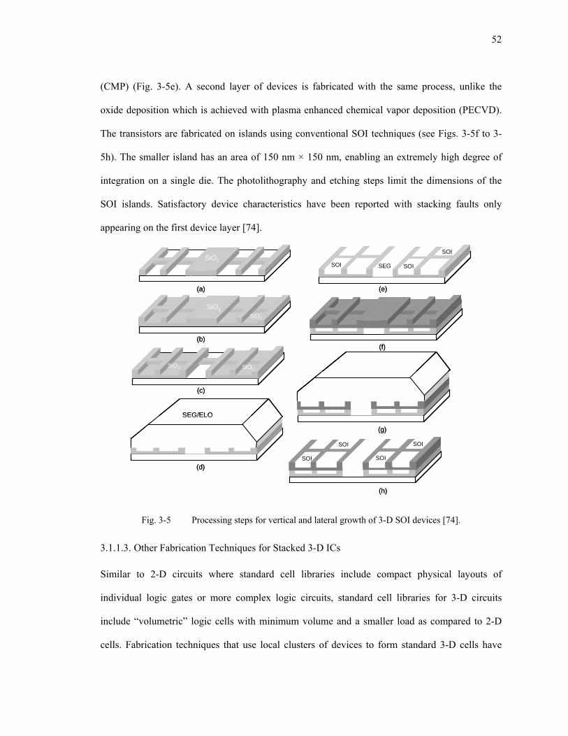
52
(CMP) (Fig. 3-5e). A second layer of devices is fabricated with the same process, unlike the
oxide deposition which is achieved with plasma enhanced chemical vapor deposition (PECVD).
The transistors are fabricated on islands using conventional SOI techniques (see Figs. 3-5f to 3-
5h). The smaller island has an area of 150 nm × 150 nm, enabling an extremely high degree of
integration on a single die. The photolithography and etching steps limit the dimensions of the
SOI islands. Satisfactory device characteristics have been reported with stacking faults only
appearing on the first device layer [74].
SiO2
SiO2SiO2
SEG/ELO
SiO2 SiO2
SOI SOISEG
SOI
(a)
(b)
(c)
(d)
(e)
(f)
(g)
(h)
SOI
SOISOI
SOI
SiO2
SiO2SiO2
SiO2SiO2
SEG/ELO
SiO2 SiO2
SOI SOISEG
SOI
SOI SOISEG
SOI
(a)
(b)
(c)
(d)
(e)
(f)
(g)
(h)
SOI
SOISOI
SOI
Fig. 3-5 Processing steps for vertical and lateral growth of 3-D SOI devices [74].
3.1.1.3. Other Fabrication Techniques for Stacked 3-D ICs
Similar to 2-D circuits where standard cell libraries include compact physical layouts of
individual logic gates or more complex logic circuits, standard cell libraries for 3-D circuits
include “volumetric” logic cells with minimum volume and a smaller load as compared to 2-D
cells. Fabrication techniques that use local clusters of devices to form standard 3-D cells have

53
been developed [76] based on double-gate MOSFETS [77], [78]. The major fabrication stages for
a 3-D inverter cell are illustrated in Fig. 3-6, where a decrease of 45% in the total capacitance is
achieved. Similar improvements are demonstrated for more complex circuits, such as a 128-bit
adder, where a 42% area reduction is observed [76].
An SOI wafer is used as the first plane of the 3-D IC. The top silicon layer is thinned by
thermal oxidation and oxide etching. A thin layer of oxide and a layer of nitride are deposited as
shown in Fig. 3-6a. The wafer is patterned and shallow trench etching is used to define the active
area (Fig. 3-6b). A layer of LTO is deposited to fill the trench, which is planarized with CMP,
where the nitride behaves as the stop layer (Fig. 3-6c). The nitride film is removed and LTO is
utilized as a dummy gate. The LTO, silicon, and oxide are patterned and etched, followed by
depositing a nitride film (Fig. 3-6d). The drain and source regions for the first device layer are
created with an As+ implantation. As depicted in Fig. 3-6e, a via is opened at the drain side to
connect the terminals of the NMOS and PMOS transistors located on the second plane. The
contact is implemented as a tunneling ohmic contact. A polysilicon layer is deposited and
planarized by CMP utilizing the nitride film as the stop layer. The nitride film is etched to expose
the silicon for the channel region (Fig. 3-6f). Boron doping is used to implement the source and
drain regions of the PMOS transistor on the top layer (Fig. 3-6g). The active area for the devices
is defined by removing the LTO and the buried oxide (Fig. 3-6h). Before forming the gates for
the stacked transistors, the gate oxide is grown by thermal oxidation, as shown in Fig. 3-6i.
Finally, in situ deposition of doped polysilicon forms the gate electrodes. Note that for the gate
below the channel region of the PMOS transistor (see Fig. 3-6j), a slow deposition rate is required
to fully fill this region.

54
Single crystal Si Nitride OxidePoly-Si Metal
BOXp
Substratep
Substrate
pSubstrate
pSubstrate
n+ n+
pSubstrate
n+ n+
pSubstrate
n+ n+
(a) (b)
(c) (d)
(e)
(g) (h)
pSubstrate
(f)
n+ n+pSubstrate
pSubstrate
n+ n+
pSubstrate
pSubstrate
n+ n+
VddVssVout Vin
(i) (j)
n+ n+
Single crystal SiSingle crystal Si NitrideNitride OxideOxidePoly-SiPoly-Si MetalMetal
BOXp
Substrate
BOXp
Substratep
Substratep
Substrate
pSubstrate
pSubstrate
n+ n+pSubstrate
n+ n+
pSubstrate
n+ n+n+ n+
pSubstrate
n+ n+pSubstrate
n+ n+
(a) (b)
(c) (d)
(e)
(g) (h)
pSubstrate
(f)
n+ n+pSubstrate
n+ n+pSubstrate
pSubstrate
n+ n+pSubstrate
n+ n+
pSubstrate
pSubstrate
n+ n+
VddVssVout Vin
pSubstrate
n+ n+
VddVssVout Vin
(i) (j)
n+ n+n+ n+
Fig. 3-6 Basic processing steps for a 3-D inverter utilizing the local clustering approach [76].
3.1.2. 3-D Fin-FETs
3-D fin-FETs are based on quasi-planar fin-FETs [79] where the devices are stacked on top of
each other, thereby sharing the same gate. A schematic of a 3-D fin-FET CMOS inverter is shown
in Fig. 3-7 [80], [81]. The second device layer can be either grown on top of the first plane or,
alternatively, can be bonded from a second wafer. The most attractive feature of this technology

55
is the approximately 50% reduction in gate area and routing resources to connect the devices
within the gate. The drive current of the devices is not controlled by the width of the devices, Wn
and Wp, but rather from the corresponding fin height notated as Hn and Hp for a NMOS and
PMOS transistors, respectively, as shown in Fig. 3-7.
The major steps of a 3-D fin-CMOS process are illustrated in Fig. 3-8. A second oxide layer
behaves as the buried oxide for the second plane. A silicon film is grown on top of the buried
oxide layer. A mask for the gate, which can endure ion etching, is formed and inductively plasma
enhanced (ICP) deep reactive ion etching (DRIE) is applied to produce the fin structure, as shown
in Fig. 3-8b. The manufactured fins are almost vertical (89.5o – 90o) [80]. A polysilicon film is
deposited, surrounding the entire fin, and doped to form the gate electrode. Ions of boron and
phosphorous in appropriate dosages are implanted to define the source and drain regions of both
device layers. In this process, the NMOS transistors are located on the second plane. A portion of
the boron ions is therefore present on the top device layer. This percentage of boron however is
low, about 10% of the phosphorous concentration, resulting in negligible degradation in the
device performance of the NMOS transistors. A critical fabrication factor is the contact between
the drain regions of the top and bottom device layers. This connection is achieved with a surface-
sidewall contact, slightly increasing the total active area of the devices on the bottom plane.
PMOS Source
PMOS Drain
Insulator InsulatorInsulator
NMOS Source
NMOS DrainShared
gate
Buried oxide
Channel length, L
Hn
Hp
PMOS SourcePMOS Source
PMOS Drain
Insulator InsulatorInsulator
NMOS SourceNMOS Source
NMOS DrainShared
gate
Buried oxide
Channel length, L
Hn
Hp
Fig. 3-7 3-D stacked Fin-CMOS device [80].

56
Fabricated devices include inverters, NAND gates, and SRAM cells [80], [81], with satisfying
characteristics, such as a high subthreshold slope and voltage transfer curves with sufficient noise
margins. A disadvantage of this technology is that several additional design rules are required.
Furthermore, stacking more than two planes with multiple metal interconnection layers is not
straightforward; a common issue in all of the aforementioned techniques for stacked 3-D ICs. In
addition, most 3-D manufacturing technologies are sequential and can therefore result in long
manufacturing turnaround times. The requirement for high quality devices for each plane of the
3-D system is an important limitation in stacked 3-D ICs. Furthermore, the insulator layers
typically used as heat shields for several of these fabrication processes greatly impede the flow of
heat during normal circuit operation, resulting in unacceptably high temperatures in the upper
planes.
Alternatively, fabricating a 3-D system with vertically bonded ICs or wafers that are
individually processed can reduce the total manufacturing time without sacrificing the quality of
the devices on the upper planes of the stack. Such techniques are discussed in the following
sections.

57
OxideSecond plane
First plane
Gate mask
Gate
p+ p+
n+ n+
Gate oxide
Contact openings
Interconnects
(a)
(b)
(c)
(d)
(e)
(f)
OxideSecond plane
First plane
Gate mask
OxideSecond plane
First plane
Gate mask
Gate
p+ p+
n+ n+
Gate
p+ p+
n+ n+
Gate oxideGate oxide
Contact openingsContact openings
InterconnectsInterconnects
(a)
(b)
(c)
(d)
(e)
(f)
Fig. 3-8 Processing steps for 3-D stacked fin-CMOS, (a) formation of the gate mask, (b) etching step
to form the stacked fin, (c) deposition of oxide and polysilicon layers, (d) ion implantation to form drain
and source regions, (e) etching step to generate contact openings, and (f) metallization of the contact
openings [80].
3.2. 3-D ICs with Through Silicon or Interplane Vias
Wafer or die level 3-D integration techniques, which utilize through silicon vias, are appealing
candidates for 3-D circuits. Interplane vias offer the greatest possible reduction in wirelength with
vertical integration. In addition, each plane of a 3-D system can be processed separately,
decreasing the overall manufacturing time. As each IC of the 3-D stack is fabricated individually,

58
the yield for each individual IC can be high. A broad spectrum of fabrication techniques for 3-D
ICs has been developed. Although none of these techniques has been standardized, nearly all of
these methods share similar fabrication stages, which are illustrated in Fig. 3-9. The order of these
stages, however, may not be the same or some stages may not be used.
CMOS or SOI
CMOS or SOI
Handle wafer
CMOS or SOI
CMOS or SOI
Etching TSV
CMOS or SOI
Form through-silicon vias
Thinned wafer
(a)
(b)
(e)
Handle waferBumps
(c)
Handle wafer detachment
(d)
CMOS or SOICMOS or SOI
CMOS or SOI
Handle wafer
CMOS or SOICMOS or SOI
Handle wafer Handle wafer
CMOS or SOICMOS or SOICMOS or SOI
CMOS or SOI
Etching TSV
CMOS or SOICMOS or SOI
Etching TSV
CMOS or SOI
Form through-silicon vias
CMOS or SOICMOS or SOI
Form through-silicon vias
Thinned wafer
(a)
(b)
(e)
Handle waferHandle waferBumps
(c)
Handle wafer detachmentHandle wafer detachment
(d)
Fig. 3-9 Typical fabrication steps for a 3-D IC process, (a) wafer preparation, (b) TSV etching, (c)
wafer thinning, bumping, and handle wafer attachment, (d) wafer bonding, and (e) handle wafer removal.
Initially, CMOS or SOI wafers are separately processed producing the physical planes of the 3-
D stack, while a certain amount of active area is reserved for the through silicon vias. The

59
interplane vias are etched and filled with metal, such as tungsten (W) or copper (Cu), or even low
resistance polysilicon. In order to decrease the length of the through silicon vias, the wafers are
attached to an auxiliary wafer, usually called a “handle wafer,” and thinned to a different
thickness depending upon the technique. The alignment and bonding phase follows, as shown in
Fig. 3-9d. Finally, the handle wafer is removed from the thinned wafer and the appropriate side of
the wafer is processed and attached to another plane, if required. A broad gamut of materials and
methods exist for each of these phases, some of which are listed in Table 3-1.
TABLE 3-1 CHARACTERISTICS OF FABRICATION TECHNIQUES FOR 3-D ICS.
Process from
IC technology
Interplane vias material
Wafer thinning thickness
Alignment accuracy [µm]
Plane bonding material
Bumps Handle wafer
[82], [83] SOI W 500 nm ±3 Cu-Cu pads Yes Yes [45], [84] SOI Cu ~10 µm 1-2 polymers No No
[85] SOI/CMOS W ~10 µm N/A Cu/Sn Yes Yes [86] CMOS Cu <2 polymer No Yes [87] SOI/CMOS n+ poly –Si/W 7-35 µm ±1 epoxy adhesive Yes Yes [88] SOI Cu <1 <1 oxide fusion No Yes
Several of the proposed techniques for 3-D ICs support the integration of both CMOS and SOI
circuits [85], [87]. From a fabrication point of view, however, SOI greatly facilitates the wafer
thinning step as the buried oxide (BOX) serves as a natural etching stop layer. This situation is
due to the high selectivity of the etching solutions. Solutions with a Si to SiO2 selectivity of 300:1
are possible [82]. In addition, SOI technology can yield particularly thin wafers or planes (< 10
µm), resulting in short interplane vias. Alternatively, SOI circuits inherently suffer from poor
thermal properties due to the low thermal conductivity of the oxide [89].
The formation of the through silicon or interplane vias is an important issue in the design of
high performance 3-D ICs. This fabrication stage includes the opening of deep trenches through
the interlayer dielectric (ILD) and the metal and device layers, passivation of the trench sidewalls
from the metal layers and conductive substrate (for CMOS circuits), and filling the opening with

60
a conductive material to electrically connect the planes of the 3-D system. Due to the importance
of this fabrication stage, a more detailed discussion of interplane vias follows in Section 3.4.
Before stacking the plane, the wafers are typically thinned to decrease the overall height of the
3-D system and, therefore, the length of the interplane vias. A reduced wafer thickness, however,
cannot sustain the mechanical stresses incurred during the handling and bonding phases of the 3-
D process. The handle wafer is therefore attached to the original wafer prior to the thinning step.
A handle wafer should possess several properties including the following:
• Mechanical durability to withstand the mechanical stresses incurred during the wafer
thinning process, due to grinding and polishing, and during bonding due to compressive
and thermal forces.
• Thermal endurance to processing temperatures during wafer bonding and bumping.
• Being chemically inert to the solutions employed for wafer thinning and polishing.
• Permit simple and fast removal of the thinned wafer with appropriate solvents.
• Enhanced wafer alignment; for example, by being transparent to light.
Thinning can proceed with a variety of methods, such as grinding and etching or both,
accompanied by polishing. Various combinations can also be applied, such as a silicon wet etch
followed by CMP, mechanical grinding with CMP, mechanical grinding succeeded by a spin
etch, and dry chemical etching [84].
Accurate alignment of the thinned wafers is also a challenging task. A variety of techniques are
utilized to align the wafer, based on the precise registration of the alignment marks. These
mechanisms include infrared alignment, through wafer via holes, transparent substrates, wafer
backside alignment, and inter-substrate alignment [90]. Typical alignment precisions range from
1 µm to 5 µm (see Table 3-1). Submicrometer accuracies have also been reported [88], [90].

61
Once the wafers are aligned, the bonding step follows. If die-to-wafer or die-to-die bonding is
preferred, in order to avoid the integration of faulty dies, each wafer is diced prior to bonding and
the dies are successively bonded. An increase in the turnaround time, however, is inevitable with
this approach. Alternatively, the wafer can be diced and each die is separately tested. The known
good dies (KGD) are placed on supporting wafers. Wafer level bonding can be applied with high
yield for each plane within a 3-D system (the overall yield can be affected by later processing
steps, e.g., bonding). Face-to-face plane bonding is illustrated in Fig. 3-9d. Alternatively, back-to-
face bonding can be applied, resulting in slightly longer vertical interconnects between the planes.
In addition, face-to-face bonding can be utilized if only two planes are integrated. A third plane is
added in a back-to-face manner. Back-to-back bonding is also possible, resulting, however, in
longer TSVs.
Bonding can be achieved with adhesive materials, metal-to-metal bonds, oxide fusion, and
eutectic alloys deposited among the planes of the 3-D system [83]. Epoxies and polymers possess
good adhesive properties and are widely used. Some of these polymers are listed in Table 3-2.
Metal-to-metal bonding requires the growth of square bumps on both candidate planes for
stacking and can consist of, for example, Cu, Cu/Ta, In/Au, and Cu/Sn. A portion of these bumps
is deposited on the edge of the interplane vias, providing enhanced electrical connection between
the planes. An epoxy filler can also be used to reinforce the bonding structure. An issue that
arises in this case, however, is that the resin can result in bonding failure due to differences in the
height of the metal bumps. To avoid such failures, pyramid or conic shaped bumps have been
proposed [91]. The compressive bonding force causes the bumps to spread, excluding the resin
from the bond region, as illustrated in Fig. 3-10. Eutectic solders are also used for plane bonding
where tin is plated on the plane surface followed by heating and compression [85]. Additionally,
the temperature profile depends upon the material used for the interface and typically ranges from

62
200 oC to 400 oC to not degrade the copper inteconnections. Other highly refractory metals, such
as tungsten or doped polysilicon, can be used if higher temperatures are necessary, increasing
however the resistance of the interplane vias.
TABLE 3-2 SEVERAL MATERIALS USED FOR WAFER BONDING.
Polymer Poly aryl ethel (FLARE) [92]
Methylsilesequionexane (MSSQ) [93] Benzocyclobutene (BCB) [94]
Hydrogensilsesquioxane (HSQ) [95] Parylene-N [96]
Depending upon the bonding mechanism and material, certain requirements should be satisfied
to avoid delamination and cracking of the planes:
• Small mismatch between the coefficient of thermal expansion (CTE) of the bonding
material and the planes
• Mechanical endurance in the later processing steps
• Minimum wafer warpage
• No outgassing of the adhesives from heating which can result in void formation
• No void generation due to the presence of residues on the layer surfaces
• Successful bonding can be verified by razor tests [45], where a razor blade is used to
penetrate the interface between the planes, while other tests can include bending forces
applied to the bonded wafer.
The final processing step for a 3-D IC with interplane vias is removal of the handle wafer and
cleaning the plane surface if subsequent bonding is required. A variety of solutions can be used to
detach the handle wafer. The time to accomplish this step also depends upon the size of the wafer
[85].

63
Square bumps
Conic bump
Height difference
Resin
Bond failure
No residue presence
Square bumps
Conic bump
Height difference
Resin
Bond failure
No residue presence
Fig. 3-10 Metal-to-metal bonding; (a) square bumps and (b) conic bumps for improved bonding quality
[91].
3.3. Contactless 3-D ICs
Although the majority of the processes that have been developed for 3-D ICs utilize vertical
interconnects with some conductive material, other techniques that provide communication
among circuits located on different planes through the coupling of electric or magnetic fields have
been demonstrated. Capacitively coupled circuits are presented in subsection 3.3.1. Inductive
vertical interconnects are discussed in subsection 3.3.2.
3.3.1. Capacitively Coupled 3-D ICs
In capacitively coupled signaling, the interplane vias are replaced with small on-chip parallel
plate capacitors that provide interplane communication to the upper plane. A schematic of a
capacitively coupled 3-D system is illustrated in Fig. 3-11 [46]. A buffer is used to drive the
capacitor. The receiver circuitry, however, is more complex, as the receiver must amplify the low

64
voltage signal to produce a full swing output. In addition, the receiver circuit should be
sufficiently sensitive and fast to detect and respond to the voltage being transferred through the
coupling capacitors. The maximum voltage level that can be propagated through a coupling
capacitance Cc is [97]
intrpc
c VCCC
C∆
++=∆
∑maxV , (3-1)
where Cp is the capacitance of the capacitor plate to the substrate and adjacent interconnect
preceding the receiver. The denominator in (3-1) includes the capacitance of the transistors at the
input of the receiver.
A 5 fF capacitance has been used in [97] to transmit a signal to several receiver architectures.
This capacitance is implemented with 20 µm × 20 µm electrodes with a separation of 2.5 µm
(e.g., dielectric thickness) and a dielectric constant of 3.5. Simulations indicate correct operation
for frequencies up to 500 MHz, while measurements show successful operation for signal
transmission up to 25 MHz for a 0.5 µm CMOS technology. Smaller parallel plate capacitor
structures and improved transceiver circuitry have also been reported, yielding a communication
bandwidth of 1.23 Gb/sec [98]. For a 0.13 µm CMOS technology, the size of the capacitor
electrodes is 8 µm × 8 µm. Comparing capacitively coupled 3-D ICs with SiP where the
interplane interconnect is implemented by wiring over the chip edge (the total interconnect length
is on the order of a centimeter), a 30% improvement in delay is demonstrated. In addition, a
significant amount of dynamic power is saved with this interconnect scheme. The static power
consumed by the receiving circuitry, however, decreases the overall power savings.

65
Receiv
er
Receiv
er
TransmitterTransmitter
Power tra
nsfer
circu
itry
Vdd
Vss
Power tra
nsfer
circu
itry
Receiv
er
Receiv
er
TransmitterTransmitter
Power tra
nsfer
circu
itry
Power tra
nsfer
circu
itry
Vdd
Vss
Power tra
nsfer
circu
itry
Fig. 3-11 Capacitively coupled 3-D IC; the large plate capacitors are utilized for power transfer, while
the small plate capacitors are used for signal propagation [46].
The parasitic capacitance of the devices is greatly reduced with a silicon-on-sapphire (SOS)
technology, a type of SOI technology [46]. This situation is particularly advantageous for the
power transfer circuitry realized with a charge pump. The transceivers and charge pump circuits
have been fabricated in a 0.5 µm CMOS technology [46], utilizing capacitors with dimensions of
90 µm × 90 µm. The distance between the two planes is 10 µm. Decreasing the separation
between the planes can increase the coupling, requiring smaller capacitor plates to propagate a
signal. The capacitors used for the power exchange should be large, though, for enhanced
coupling. A prototype based on this technique provides approximately 0.1 mA current to the
devices on the upper planes. Successful operation up to 15 MHz has been demonstrated [46].
Critical factors affecting this technique are the size of the capacitors, which affects the
interconnect density, the interplane distance, and the dielectric constant of the material between
the planes, which determine the amount of coupling. Face-to-face bonding is preferable as the
distance between the planes is less. Interconnecting a 3-D IC consisting of more than two planes
with this approach, however, is a challenging task.

66
3.3.2. Inductively Coupled 3-D ICs
Inductive coupling can be an alternative for contactless communication in 3-D ICs. Each plane in
a two-plane 3-D IC accommodates a spiral inductor, located at the same horizontal coordinates
(see Fig. 3-12). The size and diameter of the inductors are based on an on-chip differential
transformer structure [99]. Inductors with a diameter of 100 µm are shown to be suitable for
signal transmission, where the inductors are separated by a distance of 20 µm. In contrast to
capacitively coupled 3-D ICs, the signal propagation is achieved through current pulses. As
compared to the capacitive coupling technique, specialized circuitry both for the transmitter and
receiver is required, dissipating greater power. A current-mode driver generates a differential
signal. The receiver amplifies the transmitted current or voltage pulses, producing a full swing
signal. Alternatively, inductive coupling does not require as small a separation of the planes as in
the capacitive coupling technique, relaxing the demand for very thin spacing between planes.
This advantage supports the integration of more than two planes for inductively coupled 3-D ICs.
Simulations indicate a 5 Gb/sec throughput with 70 ps jitter at the output, consuming
approximately 15 mW [99].
The main limitations of this technique relate to the size of the inductors, which yields a low
interconnect density as compared to the size of the interplane vias, increased power consumption
of the transceiver circuitry, and interference among adjacent on-chip inductors. Additionally,
power delivery to the upper planes is realized with galvanic connections. Consequently, the
fabrication process and cost for this type of 3-D IC is not greatly simplified as the via formation
step is not eliminated.

67
Vdd
Gnd
Vdd
Gnd
Fig. 3-12 Inductively coupled 3-D ICs. The galvanic connections are used for power delivery [99].
3.4. Vertical Interconnects for 3-D ICs
Increasing the number of planes that can be integrated into a single 3-D system is a primary
objective of three-dimensional integration. A 3-D system with high density vertical interconnects
is therefore indispensable. Vertical interconnects implemented as through silicon vias produce the
highest interconnect bandwidth within a 3-D system, as compared to wire bonding, peripheral
vertical interconnects, and solder ball arrays. Other important criteria should also be satisfied by
the fabrication process for TSVs. A fabrication process for vertical interconnects should produce
reliable and inexpensive TSVs. In addition, a TSV should exhibit low impedance characteristics.
A high TSV aspect ratio, the ratio of the diameter of the top edge to the length of the via, may
also be required for certain types of 3-D circuits. The effect of forming the TSVs on the
performance and reliability of the neighboring active devices should also be negligible.
As shown in Fig. 3-9, TSVs are formed after the active devices on each plane of the 3-D circuit
are fabricated and prior to the wafer thinning step (“via first” approach). In this case, the TSVs
are formed as blind vias exposed during the wafer thinning step. This method provides the
important advantages of compatibility with existent process flows and simplicity in wafer
handling [100]. A disadvantage of this approach is the impact on reliability, resulting from wafer
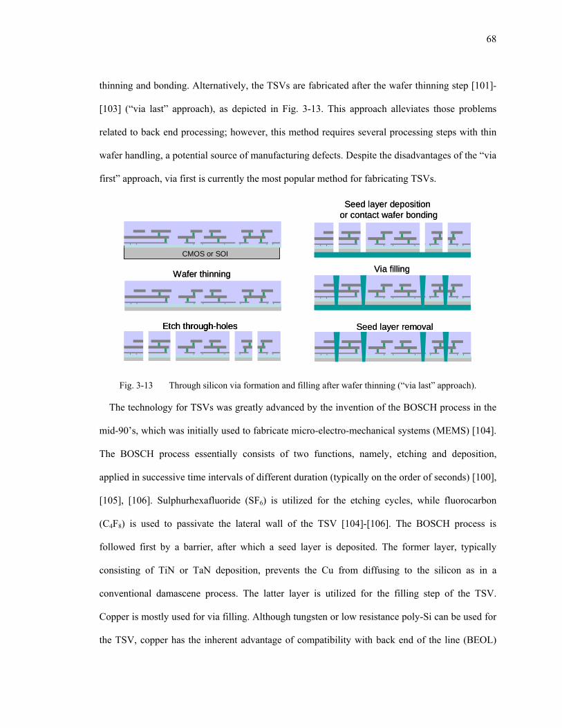
68
thinning and bonding. Alternatively, the TSVs are fabricated after the wafer thinning step [101]-
[103] (“via last” approach), as depicted in Fig. 3-13. This approach alleviates those problems
related to back end processing; however, this method requires several processing steps with thin
wafer handling, a potential source of manufacturing defects. Despite the disadvantages of the “via
first” approach, via first is currently the most popular method for fabricating TSVs.
Etch through-holes
Seed layer deposition or contact wafer bonding
CMOS or SOI
Wafer thinning Via filling
Seed layer removal Etch through-holesEtch through-holes
Seed layer deposition or contact wafer bonding
CMOS or SOICMOS or SOI
Wafer thinning Via filling
Seed layer removal
Fig. 3-13 Through silicon via formation and filling after wafer thinning (“via last” approach).
The technology for TSVs was greatly advanced by the invention of the BOSCH process in the
mid-90’s, which was initially used to fabricate micro-electro-mechanical systems (MEMS) [104].
The BOSCH process essentially consists of two functions, namely, etching and deposition,
applied in successive time intervals of different duration (typically on the order of seconds) [100],
[105], [106]. Sulphurhexafluoride (SF6) is utilized for the etching cycles, while fluorocarbon
(C4F8) is used to passivate the lateral wall of the TSV [104]-[106]. The BOSCH process is
followed first by a barrier, after which a seed layer is deposited. The former layer, typically
consisting of TiN or TaN deposition, prevents the Cu from diffusing to the silicon as in a
conventional damascene process. The latter layer is utilized for the filling step of the TSV.
Copper is mostly used for via filling. Although tungsten or low resistance poly-Si can be used for
the TSV, copper has the inherent advantage of compatibility with back end of the line (BEOL)

69
processing and the multi-layer interconnects used in modern ICs. Although the BOSCH process is
effective in etching silicon, several issues regarding the quality of the TSVs have to be considered
[100], such as
• Controllability of the via shape and tapering
• Conformal deposition and sufficient adhesion of the insulation, barrier, and seed layers
• Void-free filling with a conductive material
• Removal of excessive metal deposition along the edges of the TSV
TSVs have either a straight or tapered shape with various aspect ratios, as illustrated in Fig. 3-14.
The aspect ratio (i.e., D/W) ultimately depends upon the thickness of the wafer that results from
the wafer thinning step, where this ratio can range from 5 to 15. TSVs with a wide range of
diameter values have also been manufactured [100], [101], [104]-[109]. Tapered vias are
preferred to non-tapered vias, as a lateral wall with a slope and smooth surface facilitates the
deposition of the barrier and seed layers and the following filling step [100]. This behavior occurs
because the tapered profile decreases the effective aspect ratio of the straight segment of the TSV.
Excessive tapering, however, can be problematic, leading to V-shaped vias at the bottom edge. In
addition, a specific interconnect pitch is required at the bottom side of the via; consequently,
tapering should be carefully controlled.
W
D
(a) (b)
W
D
(a) (b)
Fig. 3-14 Through silicon via shapes, (a) straight and (b) tapered.

70
Although the BOSCH process can etch silicon sufficiently fast, producing a smooth surface,
barrier and seed layer deposition is not a straightforward task. The BOSCH process results in a
particularly rough surface, producing scallops, as illustrated in Fig. 3-15 [108]. Note that the
roughness of the surface decreases with the via depth. The rough sidewall is due to the time
multiplexed cycles of the etching and deposition steps of the BOSCH process. A low surface
roughness is of particular importance for the steps that follow the via formation process. The
scallops not only prevent a conformal barrier and seed layer deposition but also increase the
diffusion of the copper into the silicon despite the presence of the barrier layer [107].
ScallopSiO2
Si
Cu
ScallopSiO2
Si
Cu
Fig. 3-15 A schematic representation of the scallops formed due to the time-multiplexed nature of the
BOSCH process.
Various thermal loads can result from the following processing steps, such as wafer bonding,
where thermocompression is typically utilized. Finite element analysis of TSVs with a diameter
ranging from 3 µm to 10 µm has demonstrated that thermal loads contribute more to the induced
stresses on a TSV as compared to those caused by the bonding force. For specific bonding
conditions where the applied bonding force is 300 N and the temperature ranges from 300 oC to
400 oC, the thermal loads constitute 84% of the total induced stress [110]. Simulation of the
thermal loads imposed on the TSVs has indicated that the thermal stress, due to the CTE
mismatch between the dielectric and the metal filling, are more pronounced at the region where
the scallops are sharper [108]. These stresses can crack the dielectric layer, increase the current
leaking into the silicon substrate, or cause delamination of the copper within the TSV.

71
Another problem related to deep reactive ion etching concerns the silicon undercut below the
mask at the upper and wide edge of the TSV. Uncontrolled undercut can lead to mask overhang,
which in turn can accelerate plating at the top of the TSV. Faster plating of the via upper edge can
lead to premature closing of the via and to formation of a void inside the TSV [105].
Two key parameters can be used to adjust the surface roughness of the TSV sidewalls; the ratio
of the time duration of the etching and passivation steps and the flow of the C4F8 [106]. In
addition, variations of the BOSCH process or two step processes can be used to adjust the
roughness of the TSV surface. For example, manufacturing process parameters, such as the
pressure, bias power, and etching cycle time, can be varied in time rather than maintained static
throughout the etching step. With this approach, the roughness of the surface has been decreased
from ~ 0.05 µm to ~ 0.01 µm [108].
Via formation is followed by deposition of the barrier and seed layers. The primary goal of this
step is to achieve a conformal profile throughout the TSV depth, which is increasingly difficult
for TSVs with high aspect ratios. Different chemical vapor depositions are typically utilized for
this step in order to provide good uniformity with moderate processing temperatures.
Metalorganic CVD (MOCVD) can be utilized to deposit the barrier layer. The disadvantage of
this method is poor adhesion. Alternatively, physical vapor deposition (PVD) can be applied for
layer deposition, which yields fair adhesion at low temperature. PVD, however, results in poor
uniformity.
Via filling is achieved by electroplating, where the copper filling is grown laterally on the
deposited seed layer. Alternatively, electroplating can be implemented in a bottom-up manner
where a contact wafer is attached to the bottom of the device wafer, which includes the via
openings. A major problem related to this technique is the difficulty in removing the contact
wafer, which provides the seed layer for the via filling [106]. The copper electroplating should

72
produce uniform and void-free TSVs in order to achieve high quality signal paths. Poor
electroplating conditions that result in void formation within the TSV are illustrated in Fig. 3-16.
The requirement for void-free via filling can be achieved by maintaining a constant deposition
rate throughout the via depth. Due to the tapered shape of the TSV, however, achieving a constant
deposition rate requires the continuous adjustment of various parameters of the electroplating
process. Parameters that affect the TSV filling profile, which can be altered during copper
deposition, include the solution composition, wafer rotation speed, applied current waveform,
current pulse duration, and current density [100], [105], [106]. Current waveforms, such as direct
current (DC), forward pulse current (PC), and reverse pulse current (PR), can be applied. Since
the deposition rate on the top edge of the TSV is larger than at the bottom, a low forward current
density and a high reverse current density is used to maintain a constant deposition rate [100],
[101], [106]. As filling at the bottom edge progresses, thereby closing the via opening, the current
density is appropriately adjusted to maintain a fixed deposition rate.
Another alternative to avoid via filling problems is to utilize partially filled vias [111]. A
partially filled via is shown in Fig. 3-17, where the various layers of the structure are also
illustrated. The tapering of these TSVs ranges from 75o – 80o. The non-filled metal volume of the
etched via hole is filled with benzocyclobutene (BCB), while a layer of parylene insulates the
silicon substrate from the TSVs. A concern regarding these partially filled TSVs is the electrical
resistance due to the reduced amount of plated metal. Experimental results listed in Table 3-3,
however, demonstrate that low resistance vias can be achieved. Another important issue related to
this type of TSV is that the density of metal within the volume of a 3-D circuit is reduced, while
the density of the dielectric (which fills the etched via openings) is increased. This situation
increases the thermal resistance in the vertical direction, which is the primary direction of the heat

73
flow, requiring a more aggressive thermal management policy and possibly reducing the
reliability of the circuits.
(a) (b)(a) (b)
Fig. 3-16 Schematic representation of poor TSV filling resulting in void formation (a) large void at the
bottom and (b) seam void.
Any excessive metal concentrated on the top edge of the TSV should be removed prior to
wafer bonding. This metal removal is typically implemented by CMP. A copper annealing step
can also be present either before or after the CMP step [100]. After the thick metal residue is
removed from the wafer surface, wafer thinning and bonding follows, preceded, if necessary, by a
re-wiring step. In addition to manufacturing reliable TSVs, TSVs should exhibit low impedance
characteristics, as discussed in the following section.
Handlewafer
Aluminum
Copper
Silicon device wafer
Parylene
Photoresist Photoresist
BCB
Handlewafer
Aluminum
Copper
Silicon device wafer
Parylene
Photoresist Photoresist
BCB
Fig. 3-17 Structure of partial TSV and related materials [111].

74
TABLE 3-3 RESISTANCE OF PARTIALLY FILLED TSV [111].
Via bottom diameter [µm] Via top diameter [µm] Resistance of one TSV [mΩ] 60 100 30 80 120 28
100 140 24
3.4.1. Electrical Characteristics of Through Silicon Vias
The electrical characteristics of a TSV are of primary importance in 3-D ICs. A variety of TSVs
with significantly different aspect ratios and electrical parameters have been reported [100],
[101], [105]-[109]. Some relevant examples are listed in Table 3-4. The resistance values include
the resistance of the contact on which the TSV is placed, if appropriate.
TABLE 3-4 DIMENSIONS AND ELECTRICAL CHARACTERISTICS OF THE THROUGH SILICON VIAS.
Process from Depth [µm] Diameter [µm] Total resistance [mΩ] [86] 25 4 140 [112] 30 1.2 < 350 [109] 80 5/15 9.4/2.6 [109] 150 5/15 2.7/1.9 [113] 90 75 2.4
Electrical characterization of these interconnect structures is a crucial requirement, since
electrical models are necessary to accurately describe the interconnect power and speed of a 3-D
circuit. An electrical model of a TSV is illustrated in Fig. 3-18, where the vias are modeled as an
RLC interconnect. This model is based on fitting measurements of the S-parameters with the
parameters of the model. The test vehicle is a ground-signal-ground TSV structure connected to a
coplanar waveguide. The height and diameter of the TSVs are 150 µm and 50 µm, respectively.
The value of the model impedances are listed in Table 3-5. The resistance and inductance of the
TSV structure shown in Fig. 3-18 are described, respectively, by [113]

75
TSV
CTSV
Cox Cox
Cox Cox
Csi
Csi
Csi
Csi
Gsi Gsi
Gsi Gsi
RTSVRTSV RTSV
LTSVLTSV LTSV
GND GNDSignal
SiO2
Si
CTSV
CTSV CTSVCTSV
CTSV CTSV
CTSV
Fig. 3-18 Electrical model of a TSV [113].
( ) 26.08
0
10log1 f
LLTSV
+= , (3-2)
80 101 fRRTSV += , (3-3)
where the skin effect is considered. f is the maximum signal frequency propagated through the
TSV. Comparison of these expressions with measured S-parameters [113] exhibit negligible error
for frequencies up to 20 GHz.
TABLE 3-5 PARAMETERS OF THE ELECTRICAL TSV MODEL SHOWN IN FIG. 3-18 [113].
Parameter Definition Value Cox_TSV Capacitance between TSV and thin oxide layer 910 fF
CSi Capacitance of the silicon substrate 9 fF Cox Capacitance of SiO2 on the silicon surface and fringing
capacitance between vias 3 fF
GSi Resistive losses between signal and ground TSV through the silicon substrate
1.69 m/Ω
L0 TSV inductance at 0.1 GHz 35 pH R0 TSV resistance at 0.1 GHz 12 mΩ

76
3.5. Summary
Various manufacturing technologies and related issues for 3-D ICs can be summarized as
follows:
• 3-D ICs can be realized with either a sequential or parallel manufacturing process.
Sequential processes result in monolithic structures, while parallel processes yield
polylithic structures.
• Stacked 3-D ICs are monolithic structures that significantly reduce the total gate area and
capacitance. Stacked 3-D ICs can be fabricated by laser or e-beam recrystallization and
silicon growth based on semiconductor or metal seeding.
• 3-D Fin-Fets share a fin shaped gate which can reduce the area of the logic gates; however,
the design complexity increases and cannot be easily extended to 3-D ICs with more than
two planes.
• Wafer or die level 3-D integration techniques, which utilize through silicon vias, are an
appealing candidate for 3-D circuits as these vias offer the greatest reduction in wirelength.
• Fabricating 3-D ICs with TSVs typically includes the following steps: wafer preparation,
TSV formation, wafer thinning, bumping, handle wafer attachment, wafer bonding, and
handle wafer removal.
• Plane bonding can result from adhesive materials, metal-to-metal bonds, oxide fusion, and
eutectic alloys.
• The coupling of electric or magnetic fields can be used to communicate among circuits
located on different planes, producing contactless 3-D ICs.
• Some limitations of contactless 3-D ICs are the size of the inductors and capacitors, small
distance between planes, and power delivery to the upper planes.

77
• The formation of a TSV is largely based on the BOSCH process, which consists of etching
and deposition steps, multiplexed in time. Electroplating is the most common technique for
TSV filling.
• Related problems with the BOSCH and electroplating techniques are rough surfaces, mask
undercut, and void formation.
• To produce reliable TSVs, certain parameters of the BOSCH and electroplating techniques
should be dynamically adjusted. These parameters include the solution composition, wafer
rotation speed, applied current waveform, current pulse duration, and current density.

78
Chapter 4. Interconnect Prediction Models
In deep submicrometer technologies, the interconnect resistance has increased significantly,
profoundly affecting the signal propagation characteristics across an IC. On-chip interconnects
have, therefore, become the primary focus in modern circuit design. Considering the broad gamut
of interconnect issues, such as speed, power consumption, and signal integrity, beginning the
interconnect design process early in the overall design cycle can prevent expensive iterations at
later design stages, which increase both the design turnaround time and the cost of developing a
circuit. Early and accurate estimates of interconnect related parameters, such as the required
metal resources, maximum and average wirelength, and wirelength distribution are, therefore,
indispensable for deciding upon the nature of the interconnect architecture within a circuit.
Interconnect prediction models aim at providing an interconnect length distribution of a circuit
without any prior knowledge of the physical design of the circuit. This a priori distribution can be
utilized in a general interconnect prediction framework, producing estimates for various design
objectives. Interconnect prediction models have existed for a long time. Recently these models
have evolved to consider interconnect issues, such as placement and routing for interconnect
dominated circuits, interconnect delay, and crosstalk noise. The majority of these models is based
on either empirical heuristics or rules [114], [115]. A well known rule, Rent’s rule, forms the
basis for the majority of interconnect prediction models. This rule and a related interconnect
prediction model for 2-D circuits are discussed in the following section. Several interconnect
prediction models adapted for 3-D circuits are presented in Section 4.2. Projections for 3-D
circuits obtained from these models that demonstrate the opportunities of vertical integration are
discussed in Section 4.3. The key points of this chapter are summarized in Section 4.4.

79
4.1. Interconnect Prediction Models for 2-D Circuits
The cornerstone for the vast majority of wirelength prediction models is an empirical expression
known as Rent’s rule developed in the early 60’s [114]. Although the derivation of this rule was
based on partitions of circuits consisting of only tens of thousands of gates, the applicability of
this rule has been demonstrated for numerous and more complex circuits containing millions of
gates [116]-[118]. Rent’s rule is described by a simple expression,
pkNT = , (4-1)
correlating the number of I/O terminals of a circuit block with the number of circuit elements that
are contained in this block. T and N are the number of terminals and elements of a circuit block,
respectively. k is the average number of terminals per circuit element, and p is an empirical
exponent. A circuit element is an abstraction and does not refer to a specific circuit; consequently,
a circuit element can vary from a simple logic gate to a highly complex circuit. In addition, each
circuit block has a limited number of terminals and a specific circuit element capacity. The type
of circuit and partition algorithm determines the specific value of k and p [114]. Although the
parameter p has initially been determined to be in the range of 0.57 ≤ p ≤ 0.75, greater values for
p have been also observed. In general, the parameter p increases as the level of parallelism of a
system increases [115], [119].
Determining the interconnect length distribution is equivalent to enumerating the number of
connections i2-D(l) for each possible interconnect length l within a circuit. Such an enumeration,
however, is a formidable task. To circumvent this difficulty, a less computationally expensive
approach can be utilized [120], [121]. Beginning with an infinite homogeneous sea of gates as
illustrated in Fig. 4-1, the number of interconnects within an IC with length l is determined as
)()()( 22 lIlMli gpDD −− = , (4-2)

80
NA l
NC
NB
NA l
NC
NB
Fig. 4-1 An example of the method used to determine the distribution of the interconnect length.
Group NA includes one gate, group NB includes the gates located at a distance smaller than l (encircled by
the dashed curve), and NC is the group of gates at distance l from group NA (encircled by the solid curve). In
this example, l = 4 (the distance is measured in gate pitches) [120].
where Igp(l) is the expected number of connected gate pairs at a distance l in gate pitches and M2-
D(l) is the number of gates resulting in such pairs. In order to obtain the number of gate pairs
connected with an interconnect of length l, Rent’s rule is employed where a circuit element is
considered to be equivalent to a simple gate. Additionally, the total number of terminals,
including both the I/O terminals and the terminals connecting different circuit blocks for any
partition of the original circuit, remains the same. Furthermore, Rent’s rule can be applied to any
partitioning algorithm, since a different partitioning technique alters the empirical exponents
included in Rent’s rule, rather than the expression describing this rule. Consequently, the
expected number of interconnects between two groups of gates NA and NC located at a distance l
is
( ) ( ) ( ) ( )( )pCBA
pB
pCB
pBA
CAgp NNNNNNNN
NNaklI ++−−+++=)( , (4-3)

81
where NB is a group of gates within a distance l from group NA. To approximate the number of
interconnects between two groups of gates NA and NC separated by l gate pitches, as shown in Fig.
4-1, the following observation is used.
For a sufficiently large number of gates N, those gates that comprise group NC form a partial
manhattan circle (as the manhattan distance is the metric used to evaluate the distance among the
gates or, equivalently, the interconnect length among the gates). This situation applies to most of
the gates within a circuit except for those gates close to the periphery of the IC. Consequently,
from Fig. 4-1,
1=AN , (4-4)
)1(2)(1
1−== ∑
−
=llklN
l
kB , (4-5)
llNC 2)( = , (4-6)
where NB corresponds to the number of gates encircled within the partial manhattan circle formed
by the gates in group NC. The gates included in NC shape a partial but not full manhattan circle as
the crosshatched gates are not considered as part of NC. This elimination of gates during the
enumeration process ensures that a gate is not counted more than one time. With these
assumptions and by employing a binomial expansion, an approximate expression for Igp(l) is
obtained,
( ) ( ).222
)( 22 −−≅ pgp lppaklI (4-7)
From (4-7), the number of gate pairs connected by an interconnection of length l is a positive
and decreasing function of length for p < 1. The factor a in (4-7) considers the number of
terminals acting as sink terminals and is
..1
..of
ofa+
= , (4-8)

82
where f.o. is the average fanout of a gate. By incorporating the number of gate pairs M2-D(l),
which can be determined by simple enumeration, and using the binomial approximation for Igp(l),
the interconnect length distribution i2-D(l) can be obtained as
NlforlNllNlakli pD <≤⎟⎟
⎠
⎞⎜⎜⎝
⎛+−Γ= −
− 12232
)( )2(223
2 , (4-9)
( ) ( ) NlNforllNakli pD 22
6)( 223
2 <≤−Γ= −− , (4-10)
where Γ is a normalization factor. The cumulative interconnect density function (c.i.d.f.) that
provides the number of interconnects with a length smaller or equal to l is
∫ −− =l
DD dzzilI1
22 )()( . (4-11)
Expressions (4-9) – (4-11) provide the number and length distribution of those interconnects
within a homogeneous (i.e., circuit blocks with the same capacity and number of pins) 2-D circuit
consisting of N gates. By considering more than one device plane where each plane is populated
with identical circuit blocks, the wirelength distribution for a homogeneous 3-D circuit can be
generated. Various approaches have been followed to determine the wirelength distribution of a
3-D circuit, as described in the following section.
4.2. Interconnect Prediction Models for 3-D ICs
Several interconnect prediction models for 3-D ICs have been developed, providing early
estimates of the wirelength distribution in a 3-D system. Although these kinds of models lack any
knowledge about the physical design characteristics of a circuit, such models can be a useful tool
in the early stages of the design flow to roughly predict various characteristics of the system, such
as the maximum clock frequency, chip area, required number of metal layers, and power
consumption. Specifically, for 3-D ICs, such models are of considerable importance as a mature
commercial process technology for 3-D ICs does not yet exist. Interconnect prediction models

83
are, therefore, an effective means to estimate the opportunities of this innovative and developing
technology.
A wirelength prediction model for 3-D circuits should consider not only the interconnections
among gates located within the same plane, but also the interconnections among gates on
different device planes. Consequently, in 3-D circuits, the partial manhattan circles formed by the
gates in NC as illustrated in Fig. 4-1 become partial manhattan spheres as gate pairs exist not only
within the same plane (intraplane gate pairs) but also among gates located on different planes
(interplane gate pairs). These spheres are formed by partial manhattan circles of reduced radius,
which enclose the interplane gate pairs. A decreasing radius is utilized for the interplane gate
pairs to consider the vertical distance among the physical planes. This decreasing radius produces
a spherical region rather than a cylindrical region for enumerating the interplane gate pairs. Such
a hemisphere is illustrated in Fig. 4-2, where the vertical distance between adjacent planes is
assumed to be equal to one gate pitch. Considering different lengths for the vertical pitch results
in hemispheres with different radii.
NA
1st plane
2nd plane
3rd plane
4th plane
e e’
(a)
1st plane
2nd plane
3rd plane
4th plane
NANB
NC
(b)
NA
1st plane
2nd plane
3rd plane
4th plane
e e’
NA
1st plane
2nd plane
3rd plane
4th plane
e e’
(a)
1st plane
2nd plane
3rd plane
4th plane
NANB
NC
(b)
1st plane
2nd plane
3rd plane
4th plane
NANB
NC
(b)
Fig. 4-2 An example of the method used to determine the interconnect length distribution in 3-D
circuits, (a) partial manhattan hemisphere and (b) cross-section of the partial manhattan hemisphere along
e-e’. The gates in NB and NC are shown with light and dark gray tones, respectively [125].
The partial manhattan spheres are employed to determine the number of gates within groups
NA, NB, and NC [122]-[124]. In order to consider the particular conditions that apply to those gates

84
located close to the periphery of the circuit, which do not result in partial manhattan spheres, the
gates are separated into two categories. The first category is the “starting gates,” which denotes
those gates that can form a hemisphere with radius l. Typically, these gates are located close to
the center of the circuit and the “non-starting gates,” which denotes those gates that cannot form
partial spheres of radius l, are roughly located close to the periphery of the circuit [125]. An
example of starting and non-starting gates for a single plane is shown in Fig. 4-3. Thus, gate P
can be a starting gate forming a partial circle with radius l = 2, depicted by the solid line. In
addition, gate Q cannot be a starting gate for gate pairs at a distance l = 2. Alternatively, gate Q
can be a starting gate for gate pairs at a distance l = 1, as indicated by the dashed curve. Gate S is
a non-starting gate as a circle cannot be formed with a gate located below this gate for any
distance l. The same definition applies in the case of multiple physical planes where the circles
are substituted by spheres.
P
Q
S
l=2
l=1
Fig. 4-3 Example of starting and non-starting gates. Gates P and Q can be starting gates while S is a
non-starting gate [125].
As in a 2-D wirelength model, a circuit element consists of only one gate. The gates included
in groups NA, NB, and NC, for a 3-D circuit, are [122]
1=AN , (4-12)

85
∑−
−=
1
1)()(
l
iCB iNlN , (4-13)
)()()( 3
lNlMlN
start
DC
−= , (4-14)
where M3-D(l) is the number of gate pairs at a distance l in a 3-D circuit,
∑−
=−−− −+=
1
1223 )(2)()(
n
ivDDD idlMlMlM . (4-15)
The first term in (4-15) considers the intraplane gate pairs, while the second term includes the
interplane gate pairs formed in the remaining n-1 planes. The necessary expressions to determine
the number of starting gates Nstart(l) are presented in Appendix A.
Evaluating the starting and non-starting gate pairs requires a significant number of
summations. Alternatively, this differentiation between the different types of gates can be
removed, resulting in a simpler approach to produce an interconnect length distribution for 3-D
circuits as discussed in [126]–[128]. In this approach, an infinite sea of gates is considered and
the physical constraint that gates located at the periphery of the circuit cannot form a partial
manhattan circle is relaxed. The average number of gates that belong to groups NA, NB, and NC for
a 3-D circuit is
1=AN , (4-16)
( ) ( )( ) ( )(( )( ) ( )
( )( ) ( )( ) ( )) ,/1111211222
1121)(
nlldnldnllldldl
lldldllllN
vv
vv
vvB
−++−−−−−++−++−−−+
−+−−−+−≈
L
LL (4-17)
( ) ( )( )
( )( ) ) ,/214224242)(
nldnlldlldlllN
v
vvC
++−−++++−++−+=
L
LL (4-18)
where n is the number of planes within the 3-D system and dv is the interplane distance between
two adjacent planes. The number of gate pairs that are l gate pitches apart, M3-D (l), is the sum of
the gate pairs within a plane Mintra(l) and the gate pairs in different physical planes Minter(l). By
removing the distinction between starting and non-starting gates, the boundary conditions of the
problem are altered. Consequently, a normalization factor Γ’ is required such that the total

86
number of interconnects of a circuit implemented in both two and three dimensions is maintained
constant.
A similar distribution for interconnections in 3-D circuits can be determined by changing the
number of gates that correspond to a circuit element, simplifying the enumeration process. Thus,
for a 3-D circuit consisting of n planes, the expected interconnections between cell pairs (and not
gate pairs) are enumerated [129], [130]. Due to this modification, the length distribution for the
horizontal and vertical wires can be separately determined from the prediction model for 2-D
circuits, as described in Section 4.1. Horizontal wires are considered only as intraplane
interconnects in each plane of a 3-D circuit. Alternatively, the vertical wires include one or more
interplane vias and can also include horizontal interconnect segments.
Since a cell is composed of n gates, the expected interconnections between cell pairs and not
gate pairs are enumerated. In other words, the groups NA, NB, and NC become
nN A = , (4-19)
)1(2)(1
1−== ∑
−
=lnlnklN
l
kB , (4-20)
nllNC 2)( = . (4-21)
In order to determine the distribution of the vertical wires, all possible connections between two
cells are considered. The possible interconnects between a pair of cells is shown in Fig. 4-4.
Using (4-19) – (4-21) and by slightly modifying the expressions for the interconnect length
distribution of the model presented in Section 4.1, the distribution of horizontal and vertical wires
in 3-D circuits is obtained.

87
Cell i Cell j
Plane n
Plane 2
Plane 1
Plane n
Plane 2
Plane 1
Cell i Cell j
Plane n
Plane 2
Plane 1
Plane n
Plane 2
Plane 1
Plane nPlane n
Plane 2Plane 2
Plane 1Plane 1
Plane nPlane n
Plane 2Plane 2
Plane 1Plane 1
Fig. 4-4 Possible vertical interconnections for two cells with each cell containing n gates [129].
In all of the interconnect length distribution models for 3-D circuits presented in this section,
an enumeration of the gate pairs is required. This process typically involves several finite series
summations. Alternatively, a hierarchical approach can be adopted to generate the wirelength
distribution within a 3-D circuit [131]. With such an approach, the 3-D system is partitioned into
K levels of hierarchy in descending order. The entire system is therefore partitioned into eight
subcircuits at level K-1, while the lowest level (level 0) consists of single gates. The interconnect
distribution of all of the interconnect lengths smaller than the maximum length (i.e., maxll ≤ ) is
determined by the following relationship,
)()()( lqlSlI = , (4-22)
where S(l) is the structural distribution of the number of all possible gate pairs. The structural
distribution is physically equivalent to the number of gate pairs M2-D(l), as applied to the model
presented in Section 4.1. The process of calculating S(l) proceeds, however, with the method of
generating polynomials [119]. A generating polynomial of a length distribution is equivalent to
the moment generating polynomial function of that distribution and can be described by

88
∑∞
==
0)()(
l
lxlSxg , (4-23)
where each term provides the number of gate pairs connected with an interconnect of length l.
Generating polynomials can provide a more efficient representation of the length distribution, as
more complex interconnections among circuit elements can be generated by combining simple
interconnection structures and exploiting symmetries that can exist within different circuit
interconnection topologies. Consequently, the polynomials evaluated at the kth level of hierarchy
can be used to construct the polynomials of the (k+1)th level. An analysis of the technique of
generating polynomials is found in [132], [133]. The occupation probability q(l), which is the
probability of a gate pair being connected with an interconnect of length l, is based upon Rent’s
rule [114] and Donath’s approach [134] and, for a 3-D circuit, is
( )23)( −= pCllq , (4-24)
where C is a normalization constant in proportion to that constant used in the 2-D prediction
model, as discussed in the previous section.
Comparing (4-24) with (4-7), a considerable decrease is noted in the number of interconnects,
as this number decays faster as a function of length (i.e., a cubic relationship rather than a
quadratic function of length). This faster decay illustrates the reduction in the number of global
long interconnects in 3-D circuits. Exploiting this decrease in interconnect length, three-
dimensional integration is expected to offer significant improvements in several circuit design
characteristics, as discussed in the following section.
4.3. Projections for 3-D ICs
A priori interconnect prediction models described in the previous section provide an important
tool to estimate the behavior of 3-D systems and, consequently, assess the potential of this novel
technology. The introduction of the third dimension considerably alters the interconnect

89
distribution in ICs. The wire length distribution of a four million gate circuit for different
numbers of planes is illustrated in Fig. 4-5 [122]. By increasing the number of planes, the length
of the global interconnects decreases. In addition, the number of these global interconnects
decreases, while the number of short local interconnects increases such that the total number of
interconnects in the IC is essentially conserved.
100 101 102 103 10410-2
100
102
104
106
108
1010
Length in gate pitches
Inte
rcon
nect
den
sity
func
tion
2-D3-D (2 planes)3-D (4 planes)3-D (8 planes)
Fig. 4-5 Interconnect length distribution for a 2-D and 3-D IC [122].
The third dimension can be used to improve various characteristics of an IC [135], [136]. For
example, tradeoffs among the maximum clock frequency, the required number of metal layers,
and the area of an IC can be explored to achieve different design objectives. Consider a multi-tier
interconnect architecture where the metal lines in each tier have a different aspect ratio and pitch.
In addition, each tier consists of orthogonally routed multiple metal layers.

90
As a smaller area per plane is feasible in a 3-D IC, the length of the corner-to-corner
interconnects significantly decreases. Consequently, for a constant clock frequency, several
global interconnects on the upper tiers can be transferred to the local tier with a smaller aspect
ratio. The number of metal layers can therefore be reduced in 3-D circuits. Alternatively, if the
number of metal layers is not reduced by transferring the global interconnects to the local tier
interconnects, the clock frequency naturally increases as the longest distance for the clock signal
to traverse is drastically reduced. For heterogeneous 3-D ICs, the clock frequency is shown to
increase as n1.5, where n is the number of planes within a 3-D IC [137]. Furthermore, the third
dimension can be used to reduce the total area of an IC. Implementing a 2-D circuit in multiple
planes results in a decrease in the length of the interconnects, creating a timing slack. If the clock
frequency is maintained the same as that of a 2-D IC, the wiring pitch can be reduced, decreasing
the total required interconnect area. The decrease in the interconnect pitch results in an increase in
the resistive characteristics of the wires, which can consume the added timing slack provided by
the introduction of the third dimension. Consider a 100 nm ASIC consisting of 16M gates, a 3-D
IC with two planes produces a 3.9 × improvement in clock frequency, an 84% reduction in wire-
limited area, and a 25% decrease in the number of metal layers for each plane within a 3-D circuit
[123].
Since the introduction of the third dimension results, in general, in shorter interconnects, 3-D
ICs consume less power as compared to 2-D ICs. Using (4-12) – (4-15) and the expressions in
[138] to generate the interconnect distribution for a 3-D system, a circuit composed of 16M gates
is evaluated. In Fig. 4-6, the variation of the gate pitch, total interconnect length, and power
consumption are plotted versus the number of planes for two different values of the Rent’s
exponent. A value of p = 0.5 and p = 0.6 corresponds to a family of solid and dashed curves,
respectively. Since higher values of p are related to systems with higher parallelism, a greater

91
reduction in interconnect length can be achieved for these systems by increasing the number of
planes, as indicated by the curves notated by a circle. Alternatively, highly serial systems, or
equivalently, small values of the Rent’s exponent permit higher device densities, since these
circuits require fewer routing resources and, therefore, the gate pitch is significantly reduced with
the number of planes. For greater values of p, the decrease in gate pitch is smaller, as illustrated
by the dashed and solid curves notated by the square.
0 2 4 6 8 100
0.1
0.2
0.3
0.4
0.5
0.6
0.7
0.8
0.9
1
Number of planes
Nor
mal
ized
pitc
h / l
engt
h / p
ower
Gate pitchTotal lengthPower consumption
Fig. 4-6 Variation of gate pitch, total interconnect length, and interconnect power consumption with
the number of planes [138].
The interconnect power consumption depends both on the total interconnect length and the gate
pitch. As both of these parameters are reduced with the number of planes, significant savings in
power can be achieved with 3-D ICs. The sensitivity of the power consumption with respect to
the Rent’s exponent depends upon the sensitivity of the gate pitch and the total interconnect

92
length. Since these two parameters change in opposite directions with respect to the Rent’s
exponent, the sensitivity of the power consumption to this parameter is less significant (see the
curves notated by the diamond in Fig. 4-6). Overall, an improvement in power consumption of
33%, 52%, and 62% is achieved for two, four, and eight planes, respectively [138].
This analysis only considers wire limited circuits and ignores the power dissipated by the
devices. A recent analysis for 3-D circuits designed with the MITLL technology [139] also
demonstrates the advantages of the third dimension. In this investigation of 3-D circuits [140], a
Fast Fourier Transform (FFT) and an Open Reduced Instruction Set computer (RISC) Platform
System-On-Chip (ORPSOC) [141] representing a low power and a high performance circuit
example, respectively, are considered. The circuits are designed in a 180 nm SOI technology
node. Predictions for other technology nodes are also extrapolated. The signal delay, power
consumption, and silicon area for 2-D and 3-D versions of these circuits are listed in Tables 4-1
and 4-2, respectively. The clock skew and power consumption are reported in Table 4-3.
TABLE 4-1 CHARACTERISTICS OF 2-D CIRCUITS [140].
Technology node
Circuit Delay [ns] Power [mW] Area [mm2]
180 nm FFT 25.81 1050 11.61 ORPSOC 17.80 3298 18.66
90 nm FFT 21.14 439 4.18 ORPSOC 14.82 1944 6.76
45 nm FFT 14.16 334 2.32 ORPSOC 9.16 1215 3.26
TABLE 4-2 CHARACTERISTICS OF 3-D CIRCUITS [140].
Technology node
Circuit Delay [ns] Power [mW] Area [mm2]
180 nm FFT 21.49 952 4.01 ORPSOC 14.78 2933 6.72
90 nm FFT 19.54 394 1.48 ORPSOC 10.02 1551 2.42
45 nm FFT 13.01 256 0.82 ORPSOC 8.33 1029 1.29

93
TABLE 4-3 CLOCK SKEW AND POWER CONSUMPTION [140].
Technology node
Circuit Skew [ps] Power [mW] 2-D 3-D 2-D 3-D
180 nm FFT 264.3 213.4 240.5 201.9 ORPSOC 469.6 260.6 838.9 482.9
90 nm FFT 167.0 88.8 61.0 44.6 ORPSOC 317.6 213.0 694.2 419.1
45 nm FFT 106.3 68.1 66.4 48.3 ORPSOC 194.9 115.1 798.1 487.9
In addition to ASICs, general purpose systems, such as microprocessors, are also expected to
benefit considerably from vertical integration. As the speed and number of cores within a
microprocessor system increase, the demand for larger and faster cache memories also grows.
Implementing a larger cache memory inherently increases the latency of transferring data to the
cores; the memory bandwidth, however, increases. Additionally, cache misses become highly
problematic. As the total area of a microprocessor system increases, the required time for
transferring data from the processor to the main memory, due to a cache miss, also increases.
Three-dimensional integration can significantly reduce the burden of a cache miss [142].
Realizing a microprocessor system in multiple physical planes decreases the length of the data
and address busses used for transferring data between the memory and the logic. In addition, by
placing the memory on the upper planes, which consumes significantly lower power as compared
to the power consumed by the cores, the power density can be confined within acceptable levels
that will not exacerbate the overall cost of the system. Considerable improvements in speed and
the power consumed during the data transfer process in a RISC processor with various memory
planes implemented in a 3-D system have been demonstrated [143]. As compared to PCB and
MCM implementations of the same system, a RISC processor and memory system integrated on a
three plane 3-D circuit exhibits an improved performance of 61% and 49%, respectively.

94
4.4. Summary
Interconnect length distribution models for 3-D circuits are analyzed in this chapter. Based on
these models, a variety of opportunities that vertical integration offers to the IC design process is
discussed. The major points of this chapter are summarized as follows:
• Several a priori interconnect prediction models based on Rent’s rule have been
developed for 3-D ICs, unanimously demonstrating a significant decrease in the
interconnect length for such circuits.
• Rent’s rule correlates the number of terminals of a circuit with the number of modules
that constitute the circuit and the average number of terminals in each module. The
granularity of the module can vary from a single gate to an entire sub-circuit.
• The interconnect distribution within a 3-D circuit can be determined by various methods,
such as exhaustive enumeration and the method of generating polynomials.
• Vertical integration drastically alters the distribution of the interconnect lengths in a
circuit, such that the number and length of the global interconnects decreases while the
number of local interconnects increases.
• By introducing the third dimension, a variety of circuit characteristics can be improved.
For example, the performance can be increased assuming a constant total area and
number of metal layers. The number of required metal layers can be decreased for a fixed
clock frequency and total area. Furthermore, the total area can be reduced while
maintaining a fixed clock frequency.
• For heterogeneous 3-D ICs, the clock frequency is shown to increase as n1.5, where n is
the number of planes within a 3-D IC.
• Implementing a microprocessor system in multiple physical planes can reduce
unacceptably long data transfer times and alleviate the impact of cache misses.

95
Chapter 5. Physical Design Techniques for 3-D
ICs
In Chapters 2 and 3, a variety of recently developed or emerging fabrication processes for 3-D
systems are reviewed. An effective design flow, however, for 3-D ICs has yet to be developed.
This predicament is due to the additional complexity and issues that emerge from introducing the
third dimension to the integrated circuit design process. Existing techniques for 3-D circuits
primarily focus on the back end of the design process. Floorplanning, placement, and routing
techniques for standard cell 3-D circuits are presented in, respectively, Sections 5.1, 5.2, and 5.3.
These techniques constitute early research efforts to tackle these important problems rather than a
complete design flow for 3-D circuits. Furthermore, many of these techniques incorporate thermal
objectives or are exclusively dedicated to mitigate thermal problems in 3-D ICs. Although all of
these physical design techniques have several common characteristics, due to the importance of
thermal issues in three-dimensional integration, a discussion of thermal management techniques
is deferred to Chapter 6. In addition to physical design techniques, a discussion on layout tools for
3-D circuits is presented in Section 5.4. A short summary of existing design methodologies for 3-
D circuits is included in the last section of this chapter.
5.1. Floorplanning Techniques
The predominant design objective for floorplanning a 2-D circuit has traditionally been to achieve
the minimum area or, alternatively, the maximum packing density while interconnecting these
blocks with minimum length wires. Most floorplanning algorithms can be classified as either
slicing [144] or non-slicing [145], [146]. Floorplanning techniques belonging to both of these

96
categories have been proposed for 3-D circuits [148]-[151]. An efficient floorplanning technique
for 3-D circuits should adequately handle two important issues; representation of the third
dimension and the related increase in the solution space.
Certain algorithms incorporate the 3-D nature of the circuits, such as a 3-D transition closure
graph (TCG) [147], sequence triple [148], and a 3-D slicing tree [149] where the circuit blocks
are notated by a set of 3-D modules that determine the volume of the 3-D system. Utilizing such a
notation for the circuit blocks, an upper bound for 3-D slicing floorplans is determined [152]. In
3-D slicing floorplans, a plane successively bisects the volume of the 3-D system. The upper
bound for 2- and 3-D slicing floorplans is illustrated in Fig. 5-1. The coefficient r in Fig. 5-1 is
the shape flexibility ratio and denotes the maximum ratio of the dimensions of the modules (i.e.,
max(width/height, depth/height, width/depth). In general, 3-D floorplans result in larger unused
space as compared to 2-D slicing floorplans primarily due to the highly uneven volume of the 3-D
modules. For high flexibility ratios, however, this gap is considerably reduced and in certain
cases the upper bound for 3-D floorplans becomes smaller than in 2-D floorplans.
Notating the location and dimensions of these modules typically requires a considerable
amount of storage. A 3-D circuit, however, consists of a limited number of planes where the
circuit blocks can be placed. Consequently, a 3-D system can be described as an array of two-
dimensional planes where the circuit blocks are treated as rectangles that can be placed on any of
the planes constituting the 3-D circuit [151]-[154]. The second challenge for 3-D floorplanning is
to effectively explore the solution space, where a multi-step approach can often be more efficient
for floorplanning 3-D circuits than a flat approach, as discussed in the following subsection.

97
0 50 100 1501
1.05
1.1
1.15
1.2
1.25
1.3
1.35
1.4
1.45
1.5
Vtotal/Vmax (Atotal/Amax)
Vol
(F)
(Are
a(F)
)
r = 2r = 20r = 200
Fig. 5-1 Area and volume upper bounds for two- and three-dimensional slicing floorplans are depicted
by the solid and dashed curve, respectively, for different shape aspect ratio. Vtotal (Atotal) and Vmax (Amax) are
the total and maximum volume (area) respectively of a 3-D (2-D) system [152].
5.1.1. Single versus Multi-Step Floorplanning for 3-D ICs
In 2-D circuits, a flat single step approach is applied to generate a floorplan. Alternatively, in 3-D
circuits, a multi-step floorplanning technique is applied, where the blocks of a 3-D circuit are
initially partitioned into planes of a stack [150]. A comparison between these two approaches is
illustrated in Fig. 5-2.
In single step floorplanning algorithms, the floorplanning process proceeds by assigning the
blocks to the planes of the stack followed by simultaneous intraplane and interplane block
swapping, as depicted in Fig. 5-2. Alternatively, a multi-step approach does not allow interplane
moves after the partitioning step. The reason for this constraint is that interplane moves among
blocks result in a formidable increase in the solution space, directly affecting the computational
time of a multi-step floorplanning algorithm. Indeed, assuming N blocks of a 3-D system

98
consisting of n planes, a flat floorplanning approach increases the number of candidate solutions
by Nn-1/(n-1)! times as compared to a 2-D circuit consisting of the same number of blocks. The
solution space for floorplanning 2-D circuits based on the TCG technique [147], and 3-D circuits
with a single and multi-step approach are listed in Table 5-1. Consequently, a multi-phase
approach can be used to significantly reduce the number of candidate solutions.
Interplanemove
Intraplanemoves
(b)(a)
Fig. 5-2 Floorplanning strategies for 3-D ICs, (a) single step approach and (b) multi-step approach
[155].

99
TABLE 5-1 SOLUTION SPACE FOR 2-D AND 3-D IC FLOORPLANNING [155].
Characteristic 2-D IC n-plane 3-D IC TCG TCG 2-D array Multi-step
Solution space 2)(N! !)1()( 21 n-/N!N n- ( )( ) knN 2!/
Ratio 1 !)1(1 n-/N n- ( )2//
/1 knkn
knn CC L
The partitioning scheme adopted in the multi-step approach plays a crucial role in determining
the compactness of a particular floorplan, as interplane moves are not allowed when
floorplanning the planes. Different partitions correspond to different subsets of the solution space
which may exclude the optimal solution(s). The objective function for partitioning should
therefore be carefully selected. The partitioning can, for example, be based on minimizing the
estimated total wirelength of the system [150]. Consequently, a partitioning problem based on
minimizing the estimated total wirelength can be described as
minimize∑net
netEL , (5-1)
subject to maxVTN via ≤ , (5-2)
where ELnet is the estimated interconnect length connecting two blocks of a 3-D circuit, which can
contain both horizontal and vertical interconnect segments. TNvia is the total number of interplane
vias and Vmax is the maximum number of allowed interplane vias in a 3-D system. Optimizing (5-
1) is a difficult task as linearity and convexity are not guaranteed and, consequently,
combinatorial techniques cannot be easily applied [150]. Hence, a simulated annealing (SA)
based algorithm can be utilized to minimize (5-1). The starting point for the SA engine is
generated by randomly assigning the blocks to the planes of the system to balance the area of the
individual planes. The SA process progresses by swapping blocks between two planes or
changing the location of the blocks within one plane. The expected wirelength and number of
vertical vias are re-evaluated after each modification of the partition, where the algorithm

100
progresses until the target solution is achieved at the desired low temperature of the SA
algorithm.
As shown by (5-2), the allowed number of vias or, alternatively, the cut size, can affect the
partition of the blocks. The effect of the cut size on the generated partition and the correlation
between the cut size and the total wirelength can vary considerably in 3-D circuits [155]. A 3-D
floorplanner based on [153] with a fixed cut size has been applied to the benchmark circuits
included in the MCNC/GSRC benchmark suite [156]. Results of this evaluation indicate that
partitioning is important for circuits where the interconnects among blocks exhibit a narrow
wirelength distribution. Alternatively, circuits that include interconnects with a wide distribution
of lengths are least affected by the partitioning step. In addition, results characterizing the
relationship between the total wirelength and the allowed number of vertical interconnects across
the planes of the stack show that the total interconnect length does not strongly depend on the cut
size if the circuit consists of a small number of highly unevenly sized blocks. This behavior can
be attributed to the significant computational effort required to optimize the area of the floorplan
rather than the interconnect length. Alternatively, in circuits composed of uniformly sized blocks,
an inverse relationship between the number of vertical vias and the interconnect length is
demonstrated.
In the second phase of this technique, the floorplan of each plane of a 3-D circuit is generated.
Note that the floorplan of each of the planes is simultaneously produced. The interconnects
among those blocks that belong to different planes contribute to the total wirelength. Simulated
annealing is also utilized in the majority of floorplanning algorithms, both 2-D and 3-D circuits.
The circuit blocks are represented in three dimensions by the corner block list method [157].
Since the number of vertical vias is constrained by (5-2), the primary goal of the floorplanning
step is to minimize the total wirelength and area. To achieve the desired low temperature of the

101
SA algorithm, a candidate solution is perturbed by selecting a plane within the 3-D stack and
applying one of the moves described in [157]. The multi-step floorplanning technique is
evaluated on the MCNC and GSRC benchmark suites [156] and compared to the TCG-based 2-D
array and the combined bucket and 2-D array techniques (CBA) [154]. The results listed in Table
5-2 exhibit a small reduction, on the order of 3%, in the number of vertical vias and a significant
reduction of approximately 14% in wirelength, while the total area increases by almost 4% for
certain benchmark circuits.
TABLE 5-2 MULTI-STEP FLOORPLANNING RESULTS [150].
Benchmark TCG-based 2-D array CBA Multi-step floorplanning Area Wirelength Vias Area Wirelength Vias Area Wirelength Vias
ami33 3.52E+05 23139 106 3.44E+05 23475 111 4.16E+05 21580 108 ami49 1.49E+07 453083 191 1.27E+07 465053 203 1.42E+07 420636 198 n100 53295 97066 704 51736 90143 752 54648 74176 733 n200 51714 198885 1487 50055 175866 1361 55944 142196 1358 n300 74712 232074 1613 75294 230175 1568 79278 213538 1534 Avg. 1.00 1.17 1.03 0.96 1.14 1.02 1.00 1.00 1.00
5.1.2. Multi-Objective Floorplanning Techniques for 3-D ICs
The complexity of three-dimensional integration requires several dissimilar metrics for evaluating
efficient floorplans for 3-D circuits beyond the traditional area and wirelength metrics. These
metrics can consider, for example, the communication throughput among the circuit blocks or the
number of interplane vias. A communication based metric can be used in the design of
microprocessors, resulting in floorplans with a higher number of instructions per cycle (IPC)
[158].
In a 3-D system, blocks that communicate frequently are assigned to adjacent planes which
decrease the required interconnect length of the interblock connections. The communication
throughput is also increased while reducing the power consumed by the system. Alternatively,
blocks with high switching activities should not overlap in the vertical direction in order to ensure

102
that the temperature profile of the system remains within specified limits. Consequently, a 3-D
floorplanner should carefully balance the communication throughput with the operating
temperature.
In addition to the cut size or, equivalently, the number of interplane vias between planes, the
processing technique used to bond the planes of a 3-D circuit also affects the partition step in a
multi-step floorplanning methodology. The various bonding mechanisms employed in a 3-D
system contribute in different ways to the final floorplan. For example, front-to-front bonding
provides a large number of interplane vias with extremely short lengths, improving the
performance of those modules with a high switching activity. Furthermore, a block with a large
area can be divided into two smaller blocks assigned to adjacent planes and employs front-to-
front bonding in order to minimize the impact of the physical separation on the performance and
power consumption of the block. Alternatively, interplane vias utilized in front-to-back bonding
can adversely affect the performance of a 3-D system. The density of these vias is therefore low.
Pairs of blocks that share a small number of interblock connections can be assigned to planes
glued with front-to-back bonding.
Such a multi-objective floorplanning approach targeting microprocessor architectures is
illustrated in Fig. 5-3 where a variety of tools is utilized to characterize different parameters of
the processor functional blocks. The CACTI [159] and GENESYS [160] tools provide an
estimate of the speed, power, and area of the processor. The SimpleScalar simulator [161]
combined with the Watch [162] framework records the information exchanged across the system
to predict the power consumption of each benchmark circuit. Although a hierarchical approach is
followed in this technique, the simulated annealing engine is replaced by a slicing algorithm
based on recursive bipartitioning [163] to distribute the functional blocks of the processor onto
the planes of the 3-D stack in order to decrease the computational time.

103
CACTI GENESYS Profiler - Watch
Block netlistClock/buss
power
Leakagethermal
Microarchitecturalfloorplanning
IPC/power/thermalverification
Target frequency
Floorplan
Profile Block power
Temperature frequency scaling
Technologyparameters
Architectural description Application
Fig. 5-3 Design flow of the microarchitectural floorplanning process for 3-D microprocessors [158].
The additional objectives include area and wirelength (A/W), area and performance (A/P), area
and temperature (A/T), and area, performance, and temperature (A/P/T). Based on information
gathered from evaluating MCNC/GSRC benchmarks, A/W achieves the minimum area as
compared to the other objectives, decreasing by almost 40% the interconnect length over a 2-D
floorplan of the microarchitecture. A/P increases the IPC by 18% over A/W, while
simultaneously increasing the temperature by 19%. The more complex objective A/P/T generates
a temperature close to A/W, while the IPC is increased by 14%. In general, the performance
generated by the A/P/T objectives is bounded by the performance provided by the A/T and A/P
objectives. In addition, A/P/T achieves higher performance as compared to A/W with similar
temperatures [158].

104
5.2. Placement Techniques
Placement algorithms traditionally target minimizing the area of a circuit and the interconnect
length among the cells, while reserving space for routing the interconnect. In vertical integration,
a “placement dilemma” arises in deciding whether two circuit cells sharing a large number of
interconnects can be more closely placed within the same plane or placed on adjacent physical
planes, decreasing the interconnection length. Placing the circuit blocks on adjacent planes can
often produce the shortest wirelength to connect these blocks. An exception is the case of small
blocks within an SiP or SOP where the length of the interplane vias is greater than 100 µm. Since
interplane vias consume silicon area, possibly increasing the length of some interconnects, an
upper bound for this type of interconnect resource is necessary. Alternatively, sparse utilization of
the interplane interconnects can result in insignificant savings in wirelength.
Several approaches can be adopted for placing circuit cells within a volume [164]-[168]. The
circuit blocks can be treated, for example, as interconnected three-dimensional cells. This
approach may not depict the discrete nature of a 3-D system as the circuit blocks can only be
placed on a specific discrete number of planes; yet allows the formulation of a continuous,
differentiable, and possibly convex objective function that can be optimally solved [165]. Since
this approach does not consider the discrete number of planes available for circuit placement, a
second step – referred to as a legalization step – is required to finalize the cell and interplane via
placement of the planes within a 3-D circuit.
The length of a net connecting multiple cells can be described by the Euclidean distance among
the cells connected by this net in three dimensions [165]. Alternatively, the distance of the
terminals of a net can be adopted as the objective function to characterize the wirelength. To
consider the effect of the interplane interconnects, a weighting factor can be used to increase the
distance in the vertical direction, controlling the decision as to where to insert interplane vias.

105
This weight essentially behaves as a control parameter that favors the placement of highly
interconnected cells within the same or adjacent physical planes. In addition, algorithms that
place interplane vias without overlaps and support a design rule compliant via placement are
required [167]. To avoid overlap among interplane vias, a via placed within the bounding box of
the net may not be possible. In this case, an increase in the wirelength is inevitable. A large
weight is assigned to this additional interconnect segment to minimize the wire overhead.
Although placing an interplane via within the bounding box of a net does not increase the
wirelength, no existing placement techniques exist to determine the optimal location within this
available region. This issue is discussed in Chapters 6 and 7, where the optimum via locations
within available regions are determined.
5.2.1. Multi-Objective Placement for 3-D ICs
As with floorplanning, multi-objective placement techniques for 3-D circuits are of significant
importance. Additional objectives that affect the cell placement and wirelength are
simultaneously considered. Such objectives can include the temperature of the circuit and power
supply noise (simultaneous switching noise (SSN)). The objective function optimized in this case
is described by [169]
totaltotaltotaltotal TwDwWwAw 4321 +++ , (5-3)
where Atotal is the total area of the 3-D system, Wtotal is the total wirelength, Dtotal is the required
amount of decoupling capacitance to satisfy target noise margins, and Ttotal is the maximum
temperature of the substrate. The wi terms denote user-defined weights that control the
importance of each objective during the placement process.
In order to manage these different objectives, additional information describing the circuit
blocks is required including: (i) the current signature of each block, (ii) the number of metal

106
layers dedicated for the power distribution network and the number and location of the
power/ground pins, and (iii) the allowed voltage ripple on the power/ground lines due to
simultaneous switching noise. Based on this information, the required amount of decoupling
capacitance for each circuit can be determined.
This decoupling capacitance is distributed to the neighboring white spaces (i.e., open areas not
occupied by circuit cells). These spaces include those areas not only within the same plane but
also on adjacent physical planes. To detect the white space within each plane, a vertical
constrained graph is utilized. The upper boundary of the blocks at the ith level of the tree is
compared to the lower boundary of the blocks at the (i+1)th level of the tree. An example of
detecting white space is illustrated in Fig. 5-4.
ab c d
e f gws ws
Fig. 5-4 White space detection is illustrated by the white regions [171].
Although the white space can be extended to the adjacent planes in a 3-D IC, the decoupling
capacitance allocated to these spaces may not be sufficient to suppress the estimated SSN in
certain blocks. In these cases, the white space is expanded in the x and y directions to
accommodate additional decoupling capacitance. The expansion procedure is depicted in Fig. 5-5.
Several optimization techniques can be employed to efficiently determine the available white
regions and allocate decoupling capacitance within these regions. Simulated annealing (SA) is an
optimization algorithm typically used for this purpose, while different techniques for representing

107
the circuit blocks can be adopted, such as the sequence pair technique [170]. To reach the SA
freezing temperature, the solution generated at each iteration of the simulated annealing algorithm
is perturbed by swapping operations between pairs of blocks. These perturbations include both
intraplane and interplane swapping.
(a) (b)(a) (b)
Fig. 5-5 Block placement of an SOP (a) an initial placement and (b) an increase in the total area in the
x and y directions to extend the area of the white spaces [171].
Although simulated annealing is a robust optimization technique, the effectiveness of such a
multi-objective placement technique depends greatly on the accuracy of the physical model used
to describe the various objectives in addition to the area and wirelength of the circuit
interconnections. For example, the accuracy of the model describing the power distribution
network of a 3-D system can either result in insufficient reduction in SSN or redundant
decoupling capacitance which increases the area, power, and total wirelength and therefore the
cost of a circuit. Important traits of a power distribution network that should be considered for
SSN suppression are the impedance characteristics of the paths to the current load (i.e., the active
devices), power supply pins, and decoupling capacitor. The accuracy can be further improved by
including the parasitic series resistance and inductance of the decoupling capacitors and the
inductive impedance of the interconnect paths [172]-[174].
Different objectives can also be added to the objective function in (5-3) without significantly
modifying the solution procedure. For example, the same approach can be applied to minimize

108
wire congestion in a 3-D SOP as well as area, wirelength, and SSN. The modified objective
function in this case is described by [175]
totaltotaltotaltotal CwDwWwAw 4321 +++ , (5-4)
where Ctotal is the wire congestion. These multi-objective techniques have been applied to the
GSRC [156] and GT benchmarks [176]. Some of these results are listed in Table 5-3,
demonstrating the tradeoffs among the different design objectives [169], [171], [175]. The
improvement in wire congestion is about 4%, independent of other design objective(s).
TABLE 5-3 PLACEMENT FOR A FOUR PLANE SOP WITH DIVERSE DESIGN OBJECTIVES [169].
Circuits Area/wire driven [mm2, m, nF, oC] Decap-driven [mm2, m, nF, oC] Multi-objective[mm2, m, nF, oC] Name Size Area Wire Decap Temp Area Wire Decap Temp Area Wire Decap Temp n50 50 221 26.6 18.0 87.2 232 30.5 5.2 85.2 294 35.5 9.3 76.2
n100 100 315 66.6 78.2 86.5 343 73.1 69.2 81.7 410 77.0 77.9 78.5 n200 200 560 17.1 226.3 96.4 693 20.5 223.2 96.2 824 21.3 229.1 85.4 n300 300 846 28.6 393.8 100.1 843 28.6 393.8 100.1 844 28.6 393.8 100.1 gt100 100 191 13.2 60.8 71.0 207 16.8 42.5 70.9 264 18.6 55.2 59.2 gt300 300 238 19.6 342.5 93.2 248 22.3 334.9 99.5 256 22.3 343.9 85.3 gt400 400 270 28.1 493.1 114.0 268 32.5 482.0 111.6 282 34.6 492.6 91.1 gt500 500 316 30.3 645.3 99.7 321 35.4 632.4 98.0 321 34.8 635.8 95.8
Ratio 1.00 1.00 1.00 1.00 1.07 1.13 0.97 0.99 1.18 1.19 0.99 0.90
5.3. Routing Techniques
One of the first routing approaches for 3-D ICs demonstrated the complexity of the problem, as
compared to the simpler single device layer and multiple interconnect layer routing case [177].
Alternatively, recent investigations related to channel routing in 3-D ICs show that the problem is
NP-hard [178]. Consequently, different heuristics have been considered to address routing in the
third dimension [179], [182].
A useful approach for routing 3-D circuits is to convert the routing interplane interconnect
problem into a 2-D channel routing task, as the 2-D channel routing problem has been efficiently
solved [180], [181]. A number of methods can be applied to transform the problem of routing the
interplane interconnects into a 2-D routing task, which requires utilizing some of the available

109
routing resources for the interplane routing. Interplane interconnect routing can be implemented
in five major stages including interplane channel definition, pseudo-terminal allocation,
interplane channel creation (channel alignment), detailed routing, and final channel alignment
[179]. Additional stages route the 2-D channels, both for the interplane and intraplane
interconnects, and channel ordering to determine the wire routing order for the 2-D channels.
Each of these stages includes certain subtleties that should be separately considered. For
example, a 3-D net should have two terminals in the interplane channel and, therefore, inserting
pseudo-terminals may be necessary for certain nets. In addition, aligning the channels may be
necessary due to the different 2-D channel widths. Aligning the 2-D channels with adjacent
planes of the 3-D system forms an overlapping region, which serves as an interplane routing
channel. An example of such an alignment is shown in Fig. 5-6. Since channel alignment can be
necessary, however, at a later stage of the algorithm, the width of the 2-D channels is based on a
detailed route of these channels without wires. Detailed channel routing with safe ordering
follows all of the 2-D channels for both the intraplane and interplane interconnects, where a
simulated annealing scheme is utilized. The technique is completed, if necessary, with a final
channel alignment. Such an approach has been applied to randomly generated circuits and has
produced satisfactory results [179].
Cell
Plane i Plane (i+1)
Channel 1
Channel 2
Channel 1
Channel 2
Plane i Plane (i+1)
Channel 1
Channel 2
Channel 1
Channel 2
Channel 1
Channel 2
Interplane routing layers
Cell
Plane i Plane (i+1)
Channel 1
Channel 2
Channel 1
Channel 2
Plane i Plane (i+1)
Channel 1
Channel 2
Channel 1
Channel 2
Channel 1
Channel 2
Interplane routing layers
Fig. 5-6 Channel alignment procedure to create the interplane routing channels [179].
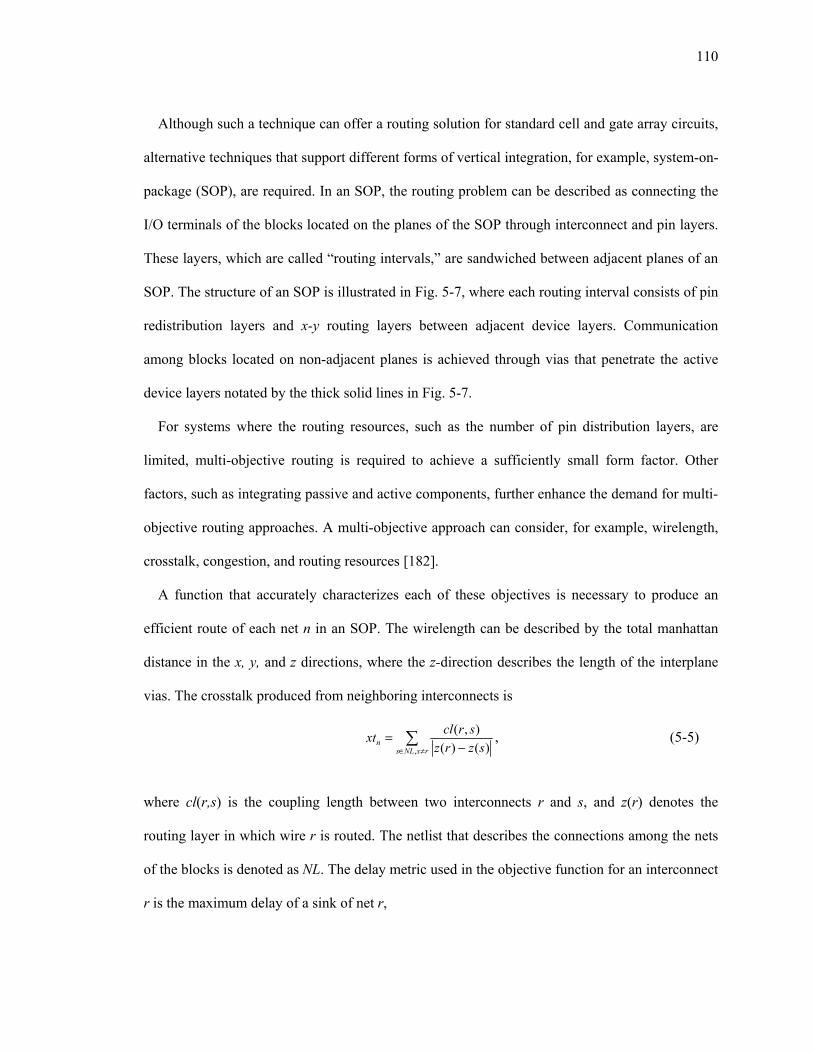
110
Although such a technique can offer a routing solution for standard cell and gate array circuits,
alternative techniques that support different forms of vertical integration, for example, system-on-
package (SOP), are required. In an SOP, the routing problem can be described as connecting the
I/O terminals of the blocks located on the planes of the SOP through interconnect and pin layers.
These layers, which are called “routing intervals,” are sandwiched between adjacent planes of an
SOP. The structure of an SOP is illustrated in Fig. 5-7, where each routing interval consists of pin
redistribution layers and x-y routing layers between adjacent device layers. Communication
among blocks located on non-adjacent planes is achieved through vias that penetrate the active
device layers notated by the thick solid lines in Fig. 5-7.
For systems where the routing resources, such as the number of pin distribution layers, are
limited, multi-objective routing is required to achieve a sufficiently small form factor. Other
factors, such as integrating passive and active components, further enhance the demand for multi-
objective routing approaches. A multi-objective approach can consider, for example, wirelength,
crosstalk, congestion, and routing resources [182].
A function that accurately characterizes each of these objectives is necessary to produce an
efficient route of each net n in an SOP. The wirelength can be described by the total manhattan
distance in the x, y, and z directions, where the z-direction describes the length of the interplane
vias. The crosstalk produced from neighboring interconnects is
∑≠∈ −
=rsNLs
n szrzsrclxt
, )()(),( , (5-5)
where cl(r,s) is the coupling length between two interconnects r and s, and z(r) denotes the
routing layer in which wire r is routed. The netlist that describes the connections among the nets
of the blocks is denoted as NL. The delay metric used in the objective function for an interconnect
r is the maximum delay of a sink of net r,

111
|maxmax NLrdD r ∈= . (5-6)
Finally, the total number of layers used to route an SOP consisting of n planes can be written as
( )∑≤≤
++=ni
brttot iLiLiLL
1)()()( . (5-7)
For each routing interval i, Lt(i), Lr(i), and Lb(i) denote the top pin distribution layer, routing
layers, and bottom pin distribution layer, respectively. Combining (5-5) - (5-7), the global route
of an SOP can proceed by minimizing the following objective function,
( )∑∈
++++NLr
rrrtot viawlxtDL εmax δγβα , (5-8)
where viar is the number of vias included in wire r, and the factors α, β, γ, and ε correspond to
weights that characterize the significance of each of the objectives during the routing procedure.
Routing interval RI(n-1)
Routing interval RI(2)
Routing interval RI(1)
Device layer Lp(1)Top pin distr. layer Lt(1)
Top pin distr. layer Lt(2)
Top pin distr. layer Lt(n-1)
Routing layer Lr(2)
Routing layer Lr(1)
Routing layer Lr(n-1)
Device layer Lp(3)
Device layer Lp(n)
Device layer Lp(2)Bottom pin distr. layer Lb(1)
Bottom pin distr. layer Lb(2)
Bottom pin distr. layer Lb(n-1)
Fig. 5-7 An SOP consisting of n planes. The vertical dashed lines correspond to vias between the
routing layers and the thick vertical solid lines correspond to through vias that penetrate the device layers
[182].

112
The various steps of a global routing algorithm optimizing the objective function described by
(5-8) is illustrated in Fig. 5-8. In order to distribute the pins to each circuit block, two different
approaches can be followed; coarse (CPD) and detailed pin distribution (DPD). The difference
between these two methods lies in the computational time. The complexity for CPD is O(p × u ×
v), where p is the number of pins and u × v is the size of the grid on which the pins are
distributed, while the complexity for DPD is O(p2 logp), exhibiting a quadratic dependence on the
number of pins.
Pin redistribution
Topology generation
Layer assignment
Channel assignment
Local routing
Pin redistribution
Pin redistribution
Topology generationTopology
generationLayer
assignmentLayer
assignment
Channel assignment
Channel assignment
Local routingLocal routing
Fig. 5-8 Stages of a 3-D global routing algorithm [182].
A topology (i.e., Steiner tree) is generated for each of the interconnects in the routing interval
to optimize the performance of the SOP. During the layer assignment process, the assignment of
the routed wires is chosen to minimize the number of routing layers. The complexity related to
the layer assignment is O(N logN), where N is the total number of interconnects. The complexity
of the channel assignment step is O(|P|•|C|), where |P| is the number of pins and |C| is the number
of channels. The algorithm terminates with a local route of the pins at the boundaries of the block
and the pins within the routing intervals. Application of this technique to the GSRC and GT
benchmark circuits exhibits an average improvement in routing resources of 35% with an average
increase in wirelength of 14% as compared to routing that only minimizes wirelength. The
maximum improvement can reach 54% with an increase in wirelength of 24% [182].

113
5.4. Layout Tools
Beyond physical design techniques, sophisticated layout tools are a crucial component for the
back end design of three-dimensional circuits. A fundamental requirement of these tools is to
effectively depict the third dimension and, particularly, the interplane interconnects. Different
types of circuit cells for several 3-D technologies have been investigated in [183]. Layout
algorithms for these cells have also been developed that demonstrate the benefits of 3-D
integration. Other traditional features, such as impedance extraction, design rule checking, and
electrical rule checking, are also necessary.
Visualizing the third dimension is a difficult task. The first attempt to develop tools to design
3-D circuits at different abstraction levels was introduced in 1984 [184], where symbolic
illustrations of 3-D circuit cells at the technology, mask, transistor, and logic level are offered. A
recent effort in developing an advanced toolset for 3-D ICs is demonstrated in [185] and [186]
where the Magic layout tool has been extended to three dimensions (i.e., 3-D Magic). To
visualize the various planes of a 3-D circuit, each plane is illustrated on separate windows, while
special markers are introduced to notate the interplane interconnects, as shown in Fig. 5-9.
Additionally, impedance extraction is supported where the technology parameters are retrieved
from pre-defined technology files. The 3-D Magic tool is also equipped with a reliability analysis
design tool called ERNI 3-D [185]. This tool provides the capability to investigate certain
reliability issues in 3-D circuits, such as electromigration, bonding strength, and interconnect
joule heating. ERNI-3D is, however, limited to a two plane 3-D circuit structure.
A process design kit has recently been constructed by a research team from North Carolina
State University [187] for designing 3-D circuits based on the MIT Lincoln Laboratories three-
dimensional fabrication technology (MITLL) [139]. This kit is based on the commercial
Cadence® Design Framework, and offers several unique features for 3-D circuits, such as
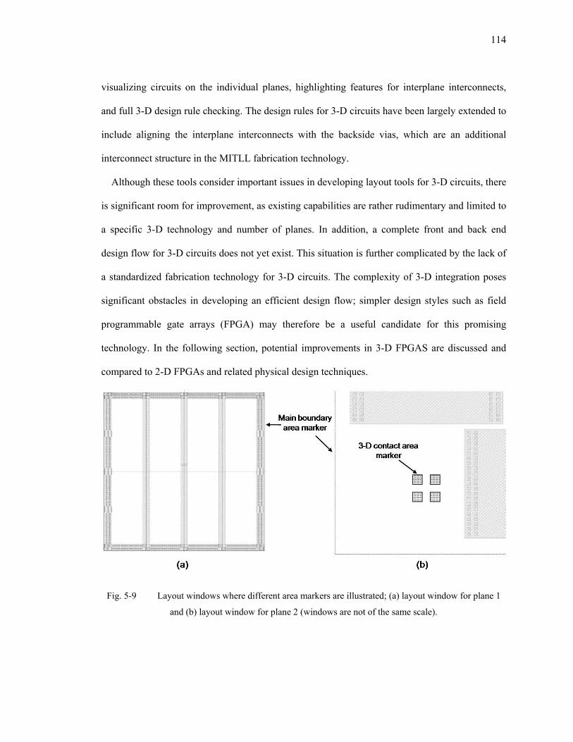
114
visualizing circuits on the individual planes, highlighting features for interplane interconnects,
and full 3-D design rule checking. The design rules for 3-D circuits have been largely extended to
include aligning the interplane interconnects with the backside vias, which are an additional
interconnect structure in the MITLL fabrication technology.
Although these tools consider important issues in developing layout tools for 3-D circuits, there
is significant room for improvement, as existing capabilities are rather rudimentary and limited to
a specific 3-D technology and number of planes. In addition, a complete front and back end
design flow for 3-D circuits does not yet exist. This situation is further complicated by the lack of
a standardized fabrication technology for 3-D circuits. The complexity of 3-D integration poses
significant obstacles in developing an efficient design flow; simpler design styles such as field
programmable gate arrays (FPGA) may therefore be a useful candidate for this promising
technology. In the following section, potential improvements in 3-D FPGAS are discussed and
compared to 2-D FPGAs and related physical design techniques.
Fig. 5-9 Layout windows where different area markers are illustrated; (a) layout window for plane 1
and (b) layout window for plane 2 (windows are not of the same scale).

115
5.5. Three-Dimensional FPGAs
Field programmable gate arrays are programmable integrated circuits that implement abstract
logic functions with a considerably smaller design turnaround time as compared to other design
styles, such as application specific (ASIC) or full custom integrated circuits. Due to this
flexibility, the share of the IC market for FPGAs has steadily increased. The tradeoff for the
reduced time to market and versatility of the FPGAs are lower speed and increased power
consumption as compared to ASICs. A traditional physical structure of an FPGA is depicted in
Fig. 5-10, where the logic blocks (LBs) can implement any digital logic function with some
sequential elements and arithmetic units [188]. The switch boxes (SBs) provide the
interconnections among the logic blocks. The SBs include pass transistors, which connect (or
disconnect) the incoming routing tracks with the outgoing routing tracks. Memory circuits control
these pass transistors and program the logic blocks for a specific application. In FPGAs, the SBs
constitute the primary delay component of the total interconnect delay between the logic blocks
and can consume a great amount of power.
Extending FPGAs to the third dimension can improve performance while decreasing overall
power consumption as compared to conventional planar FPGAs. A generalization of FPGAs to
the third dimension would include multiple planar FPGAs, wafer or die bonded to form a 3-D
system. The crucial difference between a 2-D and 3-D FPGA is the SB that provides
communication to five logic blocks rather than three neighboring logic blocks in a 2-D FPGA
(see Figs. 5-10b and 5-10c). Consequently, each incoming interconnect segment connects to five
outgoing segments rather than three outgoing segments. The situation is somewhat different for
the bottom and topmost plane of a 3-D FPGA, but in the following discussion this difference is
neglected for simplicity. Since the connectivity of a 3-D SB is greater, additional pass transistors
are required in each SB, increasing the power consumption, memory requirements to configure

116
the SB, and, possibly, the interconnect delay. The decreased interconnect length and greater
connectivity can compensate, however, for the added complexity and power of the 3-D SBs.
LBLB
LBLB LB
LB
LBLB LB
SB SB
SBSB
Channel width Fs
(a)
(b) (c)
LBLB
LBLB LB
LB
LBLB LB
SB SB
SBSB
LBLBLBLB
LBLBLBLB LBLBLB
LBLBLB
LBLBLBLB LBLBLB
SB SB
SBSB
Channel width Fs
(a)
(b) (c)
Fig. 5-10 Typical FPGA architecture, (a) a 2-D FPGA, (b) a 2-D switch box, and (c) a 3-D switch box.
A routing track can connect three outgoing tracks in a 2-D SB, while in a 3-D SB, a routing track can
connect five outgoing routing tracks [189].
In order to estimate the size of the array beyond which the third dimension is beneficial, the
authors in [189] combine the shorter average interconnect length offered by the third dimension
with the increased complexity of the SBs. Considering the hardware resources (e.g., the number
of transistors) required for each SB and the average interconnect length for a 2-D and 3-D FPGA,
the minimum number of LBs for a 3-D FPGA implementation to outperform a 2-D FPGA
implementation is determined from the solution of the following equation,
3/13,
2/12, 3
2 NFNF DsDs −− = , (5-9)
where Fs,2-D and Fs,3-D are the channel width of a 2-D and 3-D FPGA, respectively, and N is the
number of logic blocks. Solving (5-9) yields N = 244, a number that is well exceeded in modern
FPGAs.

117
Since the pass transistors, employed both in 2-D and 3-D SBs, contribute significantly to the
interconnect delay, degrading the performance of an FPGA, those interconnects that span more
than one LB can be utilized. These interconnect segments are named after the number of LBs that
is traversed by these segments, as shown in Fig. 5-11. Wires that span two, four, or even six LBs
are quite common in contemporary FPGAs. Interconnects that span one fourth to a half of an IC
edge are also possible [190].
SBSB SB SB
Six LBs
LBLB LB LB LBL1
L2 L4
SBSB SB SB
Six LBs
LBLBLBLB LBLB LBLB LBLBL1
L2 L4
Fig. 5-11 Interconnects that span more than one logic block. Li denotes the length of these interconnects
and i is the number of LBs traversed by these wires.
The opportunities that the third dimension offers in SRAM based 2-D FPGAs have also been
investigated [191]. Analytic models that estimate the channel width in 2-D FPGAs are extended
to 3-D FPGAs. Hence, the channel width for an FPGA with N LBs, exclusively consisting of unit
length interconnect segments and implemented in n physical planes, can be described by
t
dnnN
lD
en
NnN
llfW
v
⎟⎠⎞
⎜⎝⎛ −+
=∑
−+−
=−
)1(2
)()1(22
1fpga3 χ
, (5-10)
where f3-D(l) is a stochastic interconnect length distribution similar to those discussed in Chapter
4. χfpga converts a point-to-point distance into an interconnect length and et is the utilization
parameter of the wiring tracks. These two factors can be determined from statistical data

118
characterizing the placement and routing of benchmarks circuits on FPGAs. Note that these
factors depend both on the architecture of the FPGA and the automated layout algorithm.
Various characteristics of FPGAs have been estimated from benchmarks circuits and
randomized netlists placed and routed with the SEGment Allocator (SEGA) [192], the versatile
place and route (VPR) [193] tools, and analytic expressions, such as (5-10). Each FPGA is
assumed to contain 20,000 four-input LBs and is implemented in a 0.25 µm CMOS technology.
The area, channel density, and average wirelength are measured in LB pitches, which is the
distance between two adjacent LBs, and are listed in Table 5-4 for different number of physical
planes.
TABLE 5-4 AREA, WIRELENGTH, AND CHANNEL DENSITY IMPROVEMENT IN 3-D FPGAS [191].
Number of planes Area [cm2] Channel density Avg. wirelength [LB pitch] 1 (2-D) 7.84 41 8 2 (3-D) 3.1 24 6 3 (3-D) 1.77 20 5 4 (3-D) 1.21 18 5
The improvement in the interconnect delay with a length equal to the die edge is depicted in Fig.
5-12 for various number of planes. Those wires that span multiple LBs are implemented with unit
long segments (i.e., no SBs are interspersed along these wires) whereas the die edge long wires
are implemented by interconnect segments with a length equal to a quarter of the die edge. A
significant decrease in delay is projected; however, these gains diminish for more than four
planes, as indicated by the saturated portion of the delay curves depicted in Fig. 5-12. The
components of the power dissipated in a 3-D FPGA assuming a 2.5 volt power supply are shown
in Fig. 5-13. The power consumed by the LBs remains constant since the structure of the logic
blocks does not vary with the third dimension. However, due to the decreased interconnect
length, the power dissipated by the interconnects is less. This improvement, however, is smaller
than the improvement in the interconnect delay as indicated by the slope of the curves illustrated
in Figs. 5-12a and 5-12b. This behavior is attributed to the extra pass transistors in a 3-D SB,

119
which increases the power consumption, counteracting the benefit of the shorter interconnect
length. Furthermore, due to the reduced interconnect length, the power dissipated by the clock
distribution network also decreases.
Fig. 5-12 Interconnect delay for various number of physical planes [191], (a) average
length wires and (b) die edge length interconnects.
1
1.2
1.4
1.6
1.8
2
2.2
1 2 3 4
Aver
age
leng
th in
terc
onne
ct d
elay
[ns]
Number of planes
(a)
5
7
9
11
13
15
17
19
1 2 3 4
Die
edg
e lo
ng in
terc
onne
ct d
elay
[ns]
Number of planes
w/o bufferswith buffers
(b)

120
0
0.5
1
1.5
2
2.5
1 2 3 4
Pow
er c
onsu
mpt
ion
[W]
Number of planes
InterconnectsClockLBsTotal
Fig. 5-13 Power dissipated by 2-D and 3-D FPGAs [191].
A unified placement and routing system targeting various 3-D FPGA architectures [194] is
proposed in [189]. The placement technique in [189] is an extension of [195] developed for 2-D
FPGAs and follows a top-down approach where the FPGA is successively partitioned into
multiple cubic sections or cells until only one logic block is contained in each section. This
partition decomposes an FPGA into nx × ny × nz cells, where nx and ny are the number of cells in
the x and y directions, respectively, and nz is the number of planes within the 3-D FPGA. The LBs
are arranged such that the number of nets that cross a cell boundary is minimized. A simulated
annealing algorithm is employed to minimize the total interconnect length by swapping blocks
among the cells. Upon completion of the placement process, a one step routing algorithm that
utilizes a Steiner-based heuristic generates the physical route of the circuit. This heuristic, which
is based on [196], is generalized into three dimensions and iteratively applied to determine the
individual route of the nets within a 3-D FPGA that minimizes the spanning cost.
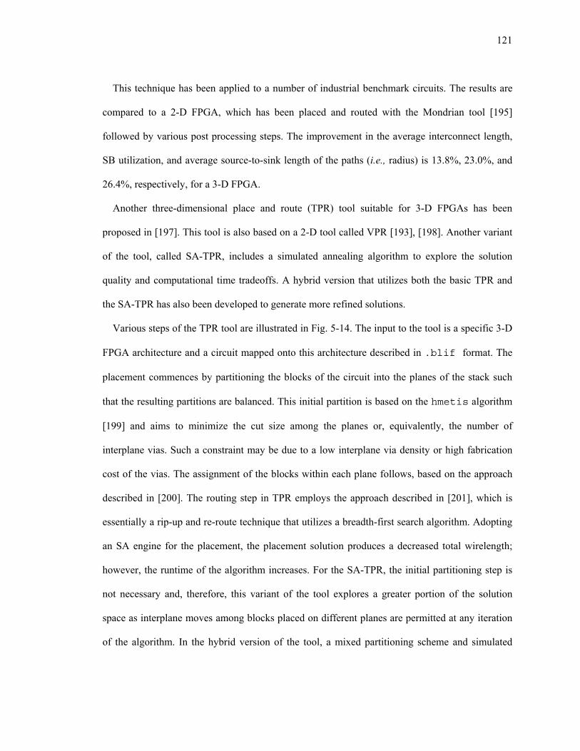
121
This technique has been applied to a number of industrial benchmark circuits. The results are
compared to a 2-D FPGA, which has been placed and routed with the Mondrian tool [195]
followed by various post processing steps. The improvement in the average interconnect length,
SB utilization, and average source-to-sink length of the paths (i.e., radius) is 13.8%, 23.0%, and
26.4%, respectively, for a 3-D FPGA.
Another three-dimensional place and route (TPR) tool suitable for 3-D FPGAs has been
proposed in [197]. This tool is also based on a 2-D tool called VPR [193], [198]. Another variant
of the tool, called SA-TPR, includes a simulated annealing algorithm to explore the solution
quality and computational time tradeoffs. A hybrid version that utilizes both the basic TPR and
the SA-TPR has also been developed to generate more refined solutions.
Various steps of the TPR tool are illustrated in Fig. 5-14. The input to the tool is a specific 3-D
FPGA architecture and a circuit mapped onto this architecture described in .blif format. The
placement commences by partitioning the blocks of the circuit into the planes of the stack such
that the resulting partitions are balanced. This initial partition is based on the hmetis algorithm
[199] and aims to minimize the cut size among the planes or, equivalently, the number of
interplane vias. Such a constraint may be due to a low interplane via density or high fabrication
cost of the vias. The assignment of the blocks within each plane follows, based on the approach
described in [200]. The routing step in TPR employs the approach described in [201], which is
essentially a rip-up and re-route technique that utilizes a breadth-first search algorithm. Adopting
an SA engine for the placement, the placement solution produces a decreased total wirelength;
however, the runtime of the algorithm increases. For the SA-TPR, the initial partitioning step is
not necessary and, therefore, this variant of the tool explores a greater portion of the solution
space as interplane moves among blocks placed on different planes are permitted at any iteration
of the algorithm. In the hybrid version of the tool, a mixed partitioning scheme and simulated

122
annealing algorithm are utilized to reduce the computational time without compromising the
quality of the solution. In Table 5-5, different variations of the TPR tool are compared with the
SA-TPR version applied to a 2-D FPGA considering various design objectives. The benefits that
result from the third dimension are evident. The target architectures for these benchmark circuits
are evaluated in terms of the gains that can be obtained by employing different interconnect
schemes in 3-D FPGAs.
TABLE 5-5 IMPROVEMENT RATIOS NORMALIZED TO THE SA-TPR OUTPUT FOR 2-D FPGAS [197].
Objective SA-TPR 3-D single
segment
SA-TPR 3-D multi
segment
TPR 2-D TPR 3-D single
segment
TPR 3-D multi
segment
Hybrid 3-D single
segment
Hybrid 3-D multi
segment Delay 0.82 0.82 1.24 0.98 0.96 0.82 0.82
Wirelength 0.90 0.90 1.34 1.06 1.05 0.85 0.83 Routing area 1.11 1.05 1.24 1.34 1.30 1.18 1.13
Channel width (horizontal)
0.93 0.91 1.23 0.95 0.96 0.85 0.82
T-VPack Circuit (.blif)
Tech. mappednetlist (.net)
Architecture
Input
TPR toolPartitioning and assignment to planes
Constraint driven placement top-to-bottom planes
3-D detailed routing
Partitioning and routing info
T-VPack Circuit (.blif)
Tech. mappednetlist (.net)
Architecture
Input
TPR toolPartitioning and assignment to planes
Constraint driven placement top-to-bottom planes
3-D detailed routing
Partitioning and routing infoPartitioning and routing info
Fig. 5-14 Design flow of a three-dimensional FPGA-based placement and routing tool [197].
These techniques assume a 3-D FPGA architecture where each plane resembles a 2-D FPGA
separately processed and stacked into a 3-D system. The primary difference is replacing the 2-D
SBs with 3-D SBs that exploit the vertical channels. In [202], another approach is followed where

123
a 2-D FPGA is implemented in three physical planes. The first plane only contains the logic
blocks, while the interconnect structure, such as the SBs, are transferred onto the second plane.
The third plane contains the memory required to configure the FPGA. With this 3-D FPGA
architecture, the goal is to redistribute the basic components of an FPGA, namely the logic
blocks, switch boxes, routing resources, and configuration memory, to maximize the integration
density within the 3-D stack. A reduction of approximately 70% in the area of a conventional
FPGA is achieved by a three plane 3-D FPGA, where the memory and SBs are located on the
upper two planes.
Utilizing the VPR tool [193] to place various circuits in a 2-D FPGA and with simple RC delay
and power models for the interconnect and pass transistors in the SBs, the delay and power
consumption of conventional FPGAs are estimated. The expressions can be optimized to evaluate
the interconnect length and delay of a 3-D FPGA. An appropriate scaling factor, smaller than one,
for the interconnects within a 3-D FPGA is used to investigate the improvements originating from
the proposed three plane architecture. For the 20 largest MCNC benchmark circuits [156], the
proposed three plane FPGA architecture offers an improvement of 3.2, 1.7, and 1.7 times in logic
density, critical path delay, and dynamic power consumption assuming a 65 nm CMOS
technology.
5.6. Summary
The physical design techniques included at the different stages of a developmental design flow
for 3-D circuits are discussed, emphasizing the particular traits of 3-D ICs. Techniques for 3-D
FPGAs are also analyzed. The major points of this chapter are summarized as follows:

124
• A variety of partitioning, floorplanning, and routing algorithms for 3-D circuits have been
developed that consider the unique characteristics of 3-D circuits. In these algorithms, the
third dimension is either fully incorporated or represented as an array of planes.
• The objective function within the 3-D layout algorithms has been extended to include
routing congestion, power supply noise, and decoupling capacitance allocation in
addition to traditional objectives, such as wirelength and area.
• Simulated annealing is an essential optimization methodology within these algorithms as
compared to greedy optimization techniques.
• Floorplanning algorithms usually consist of two basic steps, initial partitioning of the
circuit blocks onto the planes of the stack and floorplan generation for each of the planes
within the 3-D circuit.
• The partitioning step can significantly affect the quality of the solution and the
computational time of the algorithms.
• In the second stage of the floorplanning algorithms where SA is applied, solution
perturbations are realized by different intraplane moves among the blocks, such as
swapping two blocks within a plane.
• Three-dimensional FPGAs have also been proposed to improve the performance of
contemporary 2-D FPGAs, where multiple planar FPGAs are bonded to form a 3-D FPGA
stack.
• A critical issue in a 3-D FPGA is the greater complexity of the 3-D switch box that can
negate the benefits from the shorter interconnect length and the greater connectivity among
the logic blocks.

125
Chapter 6. Thermal Management Techniques
The primary advantage of three-dimensional integration, significantly greater packing density, is
also the greatest threat to this emerging technology; aggressive thermal gradients among the
planes within a 3-D IC. Thermal problems, however, are not unique to vertical integration. Due to
scaling, elevated temperatures and hot spots within traditional 2-D circuits can greatly decrease
the maximum achievable speed and affect the reliability of a circuit [203]. In addition, projected
peak temperatures greatly deviate from ITRS predictions of the maximum operating temperature
in next generation ICs [12]. Thermal awareness has, therefore, become another primary design
issue in modern integrated circuits [204], [205].
In three-dimensional integration, low operating temperature is a prominent design objective, as
thermal analysis of 3-D ICs indicates that escalated temperatures can be highly problematic [206].
Additionally, peak temperatures within a 3-D system can exceed thermal limits of existing
packaging technologies. Two key elements are required to establish a successful thermal
management strategy: the thermal model, to characterize the thermal behavior of a circuit, and
design techniques that alleviate thermal gradients among the physical planes of a 3-D stack while
maintaining the operating temperature within acceptable levels. The primary requirements of a
thermal model are high accuracy and low computational time, while thermal design techniques
should produce high quality circuits without incurring long computational design time. Although
thermal models and techniques are separately discussed, the overall effectiveness of a thermal
design methodology depends on both.
Consequently, this chapter emphasizes both the thermal models of 3-D ICs and the thermal
design methodologies that have been recently developed. Models of different accuracy and
computational speed are discussed in Section 6.1. Various techniques introduced at different steps

126
of the IC design flow to alleviate projected thermal problems are also presented. An unorthodox
yet potentially useful approach is applied here to discuss these techniques. The discussion is
based on the objective used to decrease the temperature gradients within a 3-D system, rather than
the specific design stage at which each technique is applied. Hence, those thermal strategies that
aim to improve the thermal profile of a 3-D circuit without requiring any redundant interconnect
resources for thermal management are presented in Section 6.2. Methodologies that are an
integral part of a more aggressive thermal policy that utilize thermal vias, sacrificing other design
objective(s), are outlined in Section 6.3. A synopsis of the primary points presented throughout
this chapter is provided in Section 6.4.
6.1. Thermal Analysis of 3-D ICs
A 3-D system consists of disparate materials with considerably different thermal properties
including semiconductor, metal, dielectric, and possibly polymer layers used for plane bonding
To describe the heat transfer process (only by conduction) within the volume of the system and
determine the temperature at each point, T at a steady state requires the solution of
( ) QTk −=∇∇ , (6-1)
where k is the thermal conductivity and Q is the generated heat. In integrated circuits, heat
originates from the transistors that behave as heat sources and also from self-heating of both the
devices and the interconnects (joule heating), which can significantly elevate the circuit
temperature [203], [206].
More specific techniques applied at various stage of the IC design flow, such as synthesis,
floorplanning, and placement and routing, maintain the temperature of a circuit within specified
limits or alleviate thermal gradients among the planes of the 3-D circuit. For each of the candidate
solutions, (6-1) is solved for the entire volume of the system, requiring unacceptable

127
computational time. To alleviate this issue so as to reduce the complexity of the modeling
process, standard methods to analyze heat transfer, such as finite difference, finite element, and
boundary element methods, have been adopted to evaluate the temperature of a 3-D circuit.
Simpler analytic expressions have also been developed to characterize the temperature within a 3-
D system. Each of these thermal models is described in the following subsections in ascending
order of accuracy and complexity.
6.1.1. Closed-Form Temperature Expressions
Although thermal models based on analytic expressions tend to exhibit the lowest accuracy, these
models can provide a coarse estimate of the thermal behavior of a circuit. This estimate may be of
limited value at later stages of the design process where more accurate models are required;
however, analytic models can be useful at the early stages of the design flow where physical
information about the circuit does not exist. These first order models can be used to determine
various design aspects, such as packaging and cooling strategies and estimates of the overall
system cost.
A 3-D system can be modeled as a cube consisting of multiple layers of silicon, aluminum,
silicon dioxide, and polyimide, as shown in Fig. 6-1. The devices on each plane are considered as
isotropic heat sources and are each modeled as a thin layer on the top surface of the silicon layer.
In addition, due to the short height of the 3-D stack, one-dimensional heat flow is assumed. Such
an assumption vastly decreases the simulation time. Certain boundary conditions apply to this
thermal model in order to validate the assumption of one-dimensional heat flow. Consequently,
the lateral boundaries of a 3-D IC are considered to behave adiabatically (i.e., no heat is
exchanged with the ambient through the sidewalls), which is justified as the sidewalls of a
package typically consist of insulating materials. The same assumption usually applies for the top
surface of a 3-D circuit. Alternatively, the bottom side, which is typically connected to a heat

128
sink, is treated as an isothermal surface. The insertion of these conditions limits the solution
space, decreasing the required thermal profiling time. In addition, these boundary constraints
capture the physical nature of the 3-D IC, preventing unreasonable temperatures. Note that these
boundary conditions apply to the thermal models for 3-D ICs discussed in this chapter,
independent of the accuracy and computational time of these models.
Al+SiO2
Al+SiO2
Al+SiO2Si substrate
Si substrate
Si substrate
Polyimide1st plane
2nd plane
3rd plane
Heat sources
Heat flow
Al+SiO2
Al+SiO2
Al+SiO2Si substrate
Si substrate
Si substrate
Polyimide1st plane
2nd plane
3rd plane
Heat sources
Heat flow
Fig. 6-1 Thermal model of a 3-D circuit where one-dimensional heat transfer is assumed [206].
Self-heating of MOSFET devices can also cause the temperature of a circuit to significantly
rise. Certain devices can behave as hot spots, causing significant local heating. For a two plane 3-
D structure, an increase of 24.6 oC is observed, due to the silicon dioxide and polyimide layers
acting as thermal barriers for the flow of heat towards the heat sink [206]. Although the dielectric
and glue layers behave as thermal barriers, the silicon substrate of the upper planes spreads the
heat, reducing the self-heating of the MOSFETs. Simulation results indicate that by reducing the
thickness of the silicon substrate from 3 µm to 1 µm in a two plane 3-D IC, the temperature rises
from 24.6 oC to 48.9 oC [206]. Thicker silicon substrates, however, decrease the packaging
density and increase the length of the interplane interconnects. In addition, high aspect ratio vias
can be a challenging fabrication task, as discussed in Chapter 3. If the silicon substrate is
completely removed as in the case of 3-D SOI circuits, self-heating can increase to about 200 oC,

129
which can catastrophically affect the operation of the ICs. In this model, the interconnects are
implicitly included by considering a specific aluminum density within a dielectric layer, as
depicted in Fig. 6-1.
To estimate the maximum rise in temperature on the upper planes of such a circuit while
considering the heat removal properties of the interconnects, a simple closed-form expression
based on one-dimensional heat flow has been developed. The temperature increase ∆Τ in a 2-D
circuit can be described by
APRT th=∆ , (6-2)
where Rth is the thermal resistance between the ambient environment and the actual devices, P is
the power consumption, and A is the circuit area. The power density P/A, also notated as Φ,
increases in 3-D circuits due to the smaller footprint of the circuit assuming the power
consumption remains unchanged from a 2-D circuit to a 3-D circuit. The thermal resistance also
changes, permitting (6-2) to be written as
∑ ∑= =
⎥⎦
⎤⎢⎣
⎡⎟⎠
⎞⎜⎝
⎛=∆j
i
n
ik
kij A
PRT
1, (6-3)
where Pk and Rk are the power consumption and thermal resistance of plane k, respectively.
Assuming the same power consumption and thermal resistance for all but the first of the
planes, the increase in temperature is described by [207]
⎥⎦
⎤⎢⎣
⎡⎟⎠⎞
⎜⎝⎛ −+⎟
⎠⎞
⎜⎝⎛=∆ nRRnR
APT psn 22
2 . (6-4)
The thermal resistance of the first plane includes the thermal resistance of the package and the
silicon substrate,

130
pkg
pkg
si
sips k
tk
tR += 1 , (6-5)
where tsi1 is the thickness of the silicon substrate of the first plane and ksi is the thermal
conductivity of the silicon. The thermal resistance of the upper plane k is
ifacek
ifacek
dielk
dielk
sik
sikk k
tk
tk
tR ++= , (6-6)
where tsik, tdielk, and tifacek are the thickness and ksik, kdielk, and kifacek are the thermal conductivity of
the silicon substrate, dielectric layers, and bonding interface, respectively, for plane k. From (6-
4)-(6-6), the increase in temperature on the topmost plane for various number of planes and
power densities of a 3-D system is illustrated in Fig. 6-2 for typical values of thicknesses and
thermal conductivities of the substrates, dielectrics, and bonding materials. As shown in Fig. 6-2,
the temperature increase has a square dependence on the number of planes and a linear
relationship with the power density. Note that the thermal resistance of the package provides the
greatest contribution to the temperature increase.
From Fig. 6-2, the temperature within a 3-D circuit is exacerbated even with a small number of
planes. The positive effect of the interconnects, particularly the interplane interconnects, on
removing the heat and the interconnect joule heating has not been incorporated into the
aforementioned expressions. The temperature increase on a specific plane N of a 3-D circuit
considering the heat removal properties of the interconnect and the rise in temperature due to
interconnect joule heating can be described by [208]
∑ ∑∑ ∑ ∑∑= =
−
= = +==⎟⎠⎞
⎜⎝⎛ Φ+
⎥⎥⎦
⎤
⎢⎢⎣
⎡⎟⎟⎠
⎞⎜⎜⎝
⎛Φ+=−
N
i
N
ikki
N
i
N
r
n
ijj
N
rsirirrmsambNsi RHjTT
i i
1
1
1 1 1
2,_ ρ , (6-7)

131
where the first term describes the temperature increase from the interlayer dielectrics (ILDs),
while the second term yields the rise in temperature caused by the package, the bonding
materials, and the silicon substrate(s). The notations in (6-7) are defined in Table 6-1.
02
46
8
0.2
0.4
0.6
0
200
400
600
800
Number of planes
Power density [W/mm2]
∆ T [K
]
Fig. 6-2 Temperature increase in a 3-D circuit for different number of planes and power densities
[206].
TABLE 6-1 DEFINITION OF THE SYMBOLS USED IN (6-7).
Notation Definition Tamb Ambient temperature
n Total number of planes Ni Number of metal layers in the ith plane ir rth interconnect layer in the ith plane
tILD Thickness of ILD kILD Thermal conductivity of ILD materials
s Heat spreading factor η Via correction factor, 0 ≤ η ≤ 1
jrms Root mean square value of current density for interconnects ρ Electrical resistivity of metal lines Η Thickness of interconnects Φ Total power density on the mth plane, including the power consumption of the devices
and interconnect joule heating R1 Total thermal resistance of package, heat sink, and Si substrate (bottom plane)
Ri (i>1) Thermal resistance of the bonding material and the Si substrate for each plane
Expression (6-7) considers a 1-D model of the heat flow in a 3-D system similar to that shown
in Fig. 6-1. To analytically describe this heat flow, a thermal model, where the heat sources are
represented as current sources and the thermal resistances as electrical resistors, is shown in Fig.

132
6-3. The variation in temperature at different nodes of this thermal network resembles the node
voltage in an electrical network where an Elmore delay-like model is used to determine the
temperature at these nodes.
By including interplane vias and interconnect joule heating in the thermal model of a 3-D
system, the thermal behavior of 3-D circuits can be more accurately modeled. The rise in
temperature of a two plane 3-D is determined for two scenarios. In the former, interconnect joule
heating and interplane vias are not considered, while in the latter, interconnect thermal effects are
considered. A decrease of approximately 40o in the temperature of the bottom Si substrate is
observed for the second scenario as compared to the first scenario. This result indicates the
important role that interplane vias play on reducing the overall temperature of a 3-D system by
decreasing the effective thermal resistance of the bonding and dielectric materials.
∆T1
∆T2
∆T3
Q3 I3
Q2
Q1
I2
I1
∆T3 = Q3(R3+R2+R1)+ Q2(R2+R1)+ Q1R1 R3
R2
R1
R3
R2
R1∆T1 = R1(Q3+Q2+Q1)
∆T2 = Q3(R2+R1)+ Q2(R2+R1)+ Q1R1
V3 = I3(R3+R2+R1)+ I2(R2+R1)+ I1R1
V1 = R1(I3+I2+I1)
V2 = I3(R2+R1)+ I2R2+ I1R1
∆T1
∆T2
∆T3
Q3 I3
Q2
Q1
I2
I1
∆T3 = Q3(R3+R2+R1)+ Q2(R2+R1)+ Q1R1 R3
R2
R1
R3
R2
R1∆T1 = R1(Q3+Q2+Q1)
∆T2 = Q3(R2+R1)+ Q2(R2+R1)+ Q1R1
V3 = I3(R3+R2+R1)+ I2(R2+R1)+ I1R1
V1 = R1(I3+I2+I1)
V2 = I3(R2+R1)+ I2R2+ I1R1
Fig. 6-3 An example of the duality of thermal and electrical systems.
Although (6-7) includes the effect of the interconnect on the heat flow process, the various heat
transfer paths that can exist within interconnect structures are not investigated. For example,
assuming a one-dimensional heat flow, heat is only transferred through the vertical interconnects
or, equivalently, the stacked interplane vias. Due to physical obstacles, such as circuit cells or
routing congestion, a sole vertical path may not be possible for certain interconnections. This
situation is depicted in Fig. 6-4 where different thermal paths are illustrated. As with current flow,

133
heat flow also follows the path of the highest thermal conductivity. Consequently,
interconnections consisting of horizontal segments in addition to interplane vias cause the heat
flow to deviate from the vertical direction and spread laterally for a certain length, depending
upon the length and thermal conductivity of each thermal path. By considering several thermal
paths that can exist in a 3-D circuit, as shown in Fig. 6-4, the effective thermal conductivity for
the buried interconnect layer consisting of a dielectric and metal is [209]
metalvwoxvweff kdkdk +−= )1( , (6-8)
⎥⎦
⎤⎢⎣
⎡+++=+=
321,
111RRRA
tkkkk bioxeffmetaloxeff , (6-9)
where kox, khm, and kvm are the thermal conductivity of the intralayer dielectric, intraplane
interconnects, and interplane vias, respectively. tbi, dvw, and A are the thickness of the interconnect
layer, the density of the interplane vias, and the area of the buried interconnect layer, respectively.
The thermal resistance of the paths is notated by Ri, where these paths are considered in parallel,
similar to electrical resistors connected in parallel. This duality implies that the presence of
multiple thermal paths in a region results in a decrease in the total thermal resistance of that
region.
R1 R2 R3
R1 : Metal-dielectric
R2 : Metal (horizontal and vertical)
R3 : Dielectric-metal
R1 R2 R3
R1 : Metal-dielectric
R2 : Metal (horizontal and vertical)
R3 : Dielectric-metal
Fig. 6-4 Different vertical heat transfer paths in a 3-D IC [209].
As noted above, the self-heating of devices can affect the reliability of a circuit. Those devices
that exhibit a high switching activity, such as clock drivers and buffers, can suffer considerably

134
from local heating, resulting in degraded performance. By considering the various thermal paths
that can exist within interconnect structures, the effect of a rise in temperature on these devices is
investigated where the interplane interconnects are placed below the clock driver to reduce the
self-heating process [209]. The increase in peak temperature as a function of the power density of
the clock driver placed above different interconnect structures is illustrated in Fig. 6-5. The
existence of a thermal path with a horizontal metal segment exhibits inferior heat removal
properties as compared to an exclusively vertical thermal path. In addition, the resulting increase
in temperature in a 3-D IC is higher than bulk CMOS but not necessarily worse than SOI, as
illustrated in Fig. 6-5.
50
60
70
80
90
100
110
120
130
1000 10000 100000 1000000
Power density (W/cm2)
Max
imum
tem
pera
ture
(o C)
3D hor. & ver.SOI 200 nm BOX3-D vertical onlyBulk CMOS
Fig. 6-5 Maximum temperature vs. power density for 3-D ICs, SOI, and bulk CMOS [209]. The
difference among the curves for the 3-D ICs is that the first curve (3-D horizontal and vertical) includes
thermal paths with a horizontal interconnect segment while the second curve includes only interplane vias
(only 3-D vertical vias).
Another factor that can affect the thermal profile of a circuit is the physical adjacency of the
devices. Thermal coupling among neighboring devices in a 3-D circuit is amplified, further
increasing the temperature of the circuit [206], [209]. The temperature is shown to exponentially

135
decrease with the gate pitch. This result means that the area consumed by certain circuit elements,
such as a clock driver, should be greater in a 3-D circuit than in a 2-D circuit to guarantee reliable
operation.
The assumption of one-dimensional heat flow permits a circuit to be modeled by a few serially-
connected resistors. Additionally, by including the interconnect power and the various thermal
paths, the accuracy of the thermal models of 3-D ICs is significantly improved. The major
assumption and simultaneously drawback of the closed-form expressions describing the
temperature of a 3-D circuit is that each physical plane is characterized by a single heat source.
This assumption implies that all of the heat sources that can exist within a plane collapse to a
single heat source that is included in a thermal network similar to that depicted in Fig. 6-3.
Although this approach is sufficiently accurate at early steps in the design process, knowledge of
the actual distribution of the power density and temperature within each physical plane is
essential to thermal design methodologies in order to maintain a thermally tolerant circuit
operation. More accurate models required for such techniques are presented in the following
subsection.
6.1.2. Compact Thermal Models
In the previous subsection, thermal models based on analytic expressions for the temperature of a
3-D circuit are discussed. In all of these models, the heat generated within each physical plane is
represented by a single value. Consequently, the power density of a 3-D circuit is assumed to be a
vector in the vertical direction (i.e., z-direction). In addition, the thermal network is represented as
a 1-D resistive network.
The temperature and heat within each plane of a 3-D system, however, can vary considerably,
yielding temperature and power density vectors that depend on all three directions. Compact
thermal models capture this critical information by representing the volume of a circuit with a set

136
of nodes. The nodes are connected through resistors forming a 3-D resistive network. As an
example of such a model, consider the 3-D system modeled as a thermal resistive stack shown in
Fig. 6-6. The thermal network shown in Fig. 6-6a is segmented into single pillars [210]-[212].
Each pillar is successively modeled by a 1-D thermal network including thermal resistors and
heat sources, as shown in Fig. 6-6c. The heat sources include all of the heat generated by each of
the devices contained in each tile. The resistors embedded in the gray shaded triangles are those
resistances related to the interplane vias. The absence of such a via between two planes is
incorporated by those via resistances such that heat flow will not occur through those resistors.
The voltage source at the bottom of the network models the isothermal surface between the heat
sink and the bottom silicon substrate. Additional resistors, not shown here, are used to incorporate
the flow of heat among neighboring pillars. These resistors are treated as constant as the heat flow
in the lateral directions is typically significantly smaller as compared to the vertical flow of heat.
Comparing the compact model of a single stack with the simpler 1-D model used to produce
the closed-form solution presented in subsection 6.1.1, several similarities exist. Both of these
models consist of resistors and heat sources modeled as current sources. Note that although the
voltage source included in Fig. 6-6c, which considers the heat sink, does not appear in Fig. 6-3,
this element of the model is implicitly included in (6-7) as the closed-form expression provides
the temperature rise in plane N of the 3-D system (i.e., ∆Τ = Τsi_N – Tamb) rather than the absolute
temperature generated by the compact model.

137
(a) (b) (c)
P4
R2
P3
P2
P1
Rv12
Rv11
Rp
R1
Rv22
Rv21
Rv32
Rv31
Rv13
RH
RL
RH
RL
Rv23
R3
R4 Rv33
(a) (b) (c)
P4
R2
P3
P2
P1
Rv12
Rv11
Rp
R1
Rv22
Rv21
Rv32
Rv31
Rv13
RH
RL
RH
RL
Rv23
R3
R4 Rv33
P4
R2
P3
P2
P1
Rv12
Rv11
Rp
R1
Rv22
Rv21
Rv32
Rv31
Rv13
RH
RL
RH
RL
Rv23
R3
R4 Rv33
Fig. 6-6 Thermal model of a 3-D IC, (a) a 3-D tile stack, (b) one pillar of the stack, and (c) an
equivalent thermal resistive network. R1 and Rp correspond to the thermal resistance of the thick silicon
substrate of the first plane and the thermal resistance of the package, respectively [211].
Compact thermal models provide more accurate temperature estimates as compared to analytic
expressions, but are less accurate, as are the models discussed in the following subsection. Other
issues related to compact models is that these models are independent of the boundary conditions
of the target system [213]. In addition, these models should be scalable in order to be widely
applicable. A possible solution to this requirement is appropriately scaling the resistances of the
network for each 3-D technology when calibrating the model [211].
6.1.3. Mesh Based Thermal Models
This type of model most accurately represents the thermal profile of a 3-D system. The primary
advantage of mesh based thermal models is that these models can be applied to any complex
geometry and do not depend upon the boundary conditions of the problem. A 3-D circuit is
decomposed into a 3-D structure consisting of finite hexahedral elements (i.e., parallelepipeds), as

138
illustrated in Fig. 6-7. The mesh can also be non-uniform for regions with complex geometries or
non-uniform power densities.
Fig. 6-7 A four plane 3-D circuit discretized into parallelepipeds.
The temperature at the vertices of each parallelepipeds, called a node, is evaluated from (6-1).
By considering that the thermal conductivity k is independent of the temperature, (6-1) can be
written as a linear function of temperature,
QTk −=∇2 . (6-10)
To solve this differential equation, several numerical methods, such as the finite element method
(FEM), the finite difference method, and the boundary element method are adopted [204], [214],
[215]. The temperature at any other point within a 3-D mesh is determined from different
interpolation schemes. For example, the temperature at a point within the parallelepiped shown in
Fig. 6-7 is determined from
( ) ∑=
==8
1,,
iii tNzyx NtT , (6-11)
where ti is the temperature and Ni is the shape function of node i. The shape function depends
upon two factors; the coordinates at the center of the element (xc, yc, zc) and the dimensions of the
element, as noted in Fig. 6-8 and described by
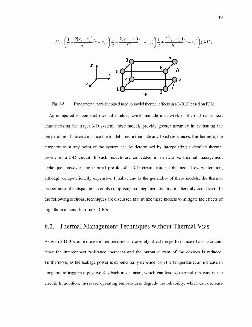
139
( ) ( ) ( ) ( ) ( ) ( )⎟
⎠
⎞⎜⎝
⎛ −−
+⎟⎠
⎞⎜⎝
⎛ −−
+⎟⎠
⎞⎜⎝
⎛ −−
−= cci
cci
cci
i zzh
zzyy
lyy
xxw
xxN 222
2212
212
21 .(6-12)
xy
z
w
h
l1 2
345
6
78
xy
z
w
h
l
xy
z
w
h
l1 2
345
6
78
Fig. 6-8 Fundamental parallelepiped used to model thermal effects in a 3-D IC based on FEM.
As compared to compact thermal models, which include a network of thermal resistances
characterizing the target 3-D system, these models provide greater accuracy in evaluating the
temperature of the circuit since the model does not include any fixed resistances. Furthermore, the
temperature at any point of the system can be determined by interpolating a detailed thermal
profile of a 3-D circuit. If such models are embedded in an iterative thermal management
technique, however, the thermal profile of a 3-D circuit can be obtained at every iteration,
although computationally expensive. Finally, due to the generality of these models, the thermal
properties of the disparate materials comprising an integrated circuit are inherently considered. In
the following sections, techniques are discussed that utilize these models to mitigate the effects of
high thermal conditions in 3-D ICs.
6.2. Thermal Management Techniques without Thermal Vias
As with 2-D ICs, an increase in temperature can severely affect the performance of a 3-D circuit,
since the interconnect resistance increases and the output current of the devices is reduced.
Furthermore, as the leakage power is exponentially dependent on the temperature, an increase in
temperature triggers a positive feedback mechanism, which can lead to thermal runaway in the
circuit. In addition, increased operating temperatures degrade the reliability, which can decrease

140
the lifetime of the circuits. The cost of a circuit can also increase as more expensive packaging is
required to handle high temperatures.
These issues are expected to be more pronounced in 3-D circuits due to the higher power
density. This increase is also enhanced by the greater distance of the heat sources (i.e., devices)
on the upper planes from the heat sink. Finally, the reduced area of the 3-D system results in a
smaller area for the heat sink, reducing the heat transferred to the ambient environment [216].
Several floorplanning, placement, and routing techniques for 3-D ICs and SOP have been
developed to consider the high temperatures and thermal gradients developed throughout the
planes of these systems beyond the traditional objectives, such as area and wirelength
minimization. In Section 6.2.1, thermal-driven floorplanning techniques are discussed, while
thermal-driven placement techniques are analyzed in Section 6.2.2.
6.2.1. Thermal-Driven Floorplanning
Traditional floorplanning techniques for 2-D circuits typically target the optimization of an
objective function that includes the total area of the circuit and the total wirelength of the
interconnections among the circuit blocks. For 3-D circuits, a further requirement for
floorplanning may be minimizing the number of interplane vias to decrease the fabrication cost
and silicon area. Consequently, an objective function for 3-D circuit floorplanning can be written
as
ivcareacwlct 321cos ++= , (6-13)
where c1, c2, and c3, are weight factors and wl, area, and iv are the normalized wirelength, area,
and number of interplane vias [217].
A thermal-driven floorplanning technique would extend this function to include the thermal
objective,

141
)(cos 4321 Tgcivcareacwlct +++= , (6-14)
where the last term is a cost function of the temperature. An example of such a function where the
cost is a ramp function of the temperature is schematically shown in Fig. 6-9 [217]. Note that the
cost function does not intersect the abscissa but rather reaches a plateau. Consequently, such an
objective function does not minimize the temperature of the circuit but rather constrains the
temperature within specified levels. Indeed, minimizing the circuit temperature may not be an
effective objective leading to prohibitively long computational times or to excessive increases in
other design objectives.
g(T)
THlow0
0
TTT −THhigh
g(T)
THlow0
0
TTT −THhigh
Fig. 6-9 Temperature cost function [217].
Another important issue for physical design techniques in 3-D circuits is the representation of
the third dimension, as also discussed in Chapter 5. A non-efficient representation scheme can
considerably increase the storage requirements and, consequently, slow down the optimization
process, irrespective of the objective function.
A low overhead representation scheme is realized by representing the blocks within a 3-D
system with a combination of 2-D matrices that correspond to the planes of the system and a
bucket structure that contains the connectivity information for the blocks located on different
planes (a combined bucket and 2-D array (CBA)) [217]. A transitive closure graph is used to
represent the intraplane connections of the circuit blocks. The bucket structure can be envisioned

142
as a group of buckets imposed on a 3-D stack. The indices of the blocks that intersect with a
bucket are included in this bucket, irrespective of the plane on which a block is located. A 2 × 2
bucket structure applied to a two plane 3-D IC is shown in Fig. 6-10, where the index of the
bucket is also depicted. To explain the bucket index notation, consider the lower left tile of the
bucket structure shown in Fig. 6-10c (i.e., b21). The indices of the blocks that intersect with this
tile on the second plane are d and e and the indices of the blocks from the first plane are l and k.
Consequently, b21 includes d, e, l, and k.
ab
c
d e
f
g h i
j
k
l
c, b, a, g a, f, h, i, j
d, e, l, k e, f, j, k
b11 b12
b21 b22
abc
d e
f
g h i
j
k
l
b11
b11
b12
b12
b21
b21
b22
b22
(a) (b) (c)
ab
c
d e
f
g h i
j
k
l
ab
c
d e
f
g h i
j
k
l
c, b, a, g a, f, h, i, j
d, e, l, k e, f, j, k
b11 b12
b21 b22
abc
d e
f
g h i
j
k
l
b11
b11
b12
b12
b21
b21
b22
b22
abc
d e
f
g h i
j
k
l
b11
b11
b12
b12
b21
b21
b22
b22
(a) (b) (c) Fig. 6-10 A bucket structure example for a two plane circuit consisting of twelve blocks [217], (a) a two
plane 3-D IC, (b) a 2 × 2 bucket structure imposed on a 3-D IC, and (c) the resulting bucket indices.
Simulated annealing (SA) is a well-known method to produce an effective solution of an
objective function, as in (6-14) for floorplanning 3-D circuits. The SA scheme converges to the
desired freezing temperature through several solution perturbations. These perturbations include
one of the following operations, some of which are unique to 3-D ICs:
(i) block rotation
(ii) intraplane block swapping
(iii) intraplane reversing of the position of two blocks
(iv) move of a block within a plane
(v) interplane swapping of two blocks
(vi) z-neighbor swap
(vii) z-neighbor move

143
The last three operations are unique to 3-D ICs, while the z-neighbor swap can be considered as a
special case of interplane swapping of two blocks. Thus, two blocks located on adjacent planes
are swapped only if the relative distance between these two blocks is small. In addition, the z-
neighbor move considers the move of a block to another plane of the 3-D system without
significantly altering the x-y coordinates. Examples of these two operations are illustrated in Fig.
6-11.
abc
d e
f
g h i
j
k
l
a
bc
d e
f
g
h
i
j
k
l
(a)
abc
d e
f
g h i
j
k
l
(b) (c)
abc
d e
f
g h i
j
k
l
abc
d e
f
g h i
j
k
l
a
bc
d e
f
g
h
i
j
k
l
aa
bc
d e
f
g
hh
i
j
k
l
(a)
abc
d e
f
g h i
j
k
l
abc
d e
f
g h i
j
k
l
abc
d e
f
g h i
j
k
ll
(b) (c) Fig. 6-11 Interplane moves, (a) an initial placement, (b) a z-neighbor swap between blocks a and h, and
(c) a z-neighbor move for block l from the first plane to the second plane.
In an exhaustive approach, each of the aforementioned block perturbations require a thermal
profile of a 3-D circuit. Such a tedious approach greatly increases the computational time of the
algorithm. A thermal profile, therefore, is invoked after specific operations or after a specified
number of iterations. The reasoning behind this practice is that certain operations, such as the
move of two intraplane blocks or the rotation of a block, is not likely to significantly affect the
temperature of the system, whereas other operations, such as a z-neighbor swap or a z-neighbor
move, is expected to considerably affect the temperature of some blocks.
As discussed in Section 6.1, the efficiency of the thermal techniques depends significantly
upon the time required for evaluating the temperature within the volume of a 3-D circuit. Thermal
models with different accuracy and computational time have been applied to MCNC benchmarks
in conjunction with this floorplanning technique. Related results are reported in Table 6-2 where

144
both the detailed and compact thermal modeling approach is considered [217]. A significant
tradeoff between the runtime and the decrease in temperature exists between these thermal
models. With thermal driven floorplanning, where a grid of resistances is utilized to thermally
model a 3-D circuit, a 56% reduction in temperature is achieved. The computational time,
however, is increased by approximately an order of magnitude as compared to conventional
floorplanning algorithms. Alternatively, if a closed-form expression is used for the thermal model
of the 3-D circuit, the decrease in temperature is only 40%. The computational time, however, is
approximately doubled in this case. Other design characteristics, such as the area and wirelength,
do not change significantly between the two models.
TABLE 6-2 TEMPERATURE DECREASE THROUGH THERMAL DRIVEN FLOORPLANNING [217].
Circuit CBA w/o thermal objective CBA-T CBA-T-fast T [oC] Runtime [sec] T [oC] Runtime [sec] T [oC] Runtime [sec]
ami33 471 23 160 466 204 56 ami49 259 86 151 521 196 144 n100 391 313 158 4322 222 446 n200 323 1994 156 6843 242 4474 n300 373 3480 167 17484 208 4953 Avg. 1 1 0.44 9.71 0.6 1.82
In an effort to decrease the computational time, floorplanning can be performed in two separate
phases. In the first step, the circuit blocks are assigned to the planes of the 3-D system to
minimize area and wirelength. This phase, however, can result in highly uneven areas among the
planes. A second step that limits these unbalances is therefore necessary. The objective function
to accomplish this balancing process can be described as
TOPcPcFdevcareacwlct ⋅+⋅+⋅+⋅+⋅= 54321 )(cos , (6-15)
where c1, c2, c3, c4, and c5 notate some weighting factors. Beyond the first two terms that include
the area and wirelength of the circuit, the remaining terms consider other possible design
objectives for 3-D circuits. The third term is intended to minimize the unbalance that can exist
among the dimensions of the planes within the stack, based on the deviation dimension approach

145
described in [153]. Planes with particularly different areas or greatly uneven dimensions can
result in a significant portion of unoccupied silicon area on each plane.
The last two terms in (6-15) consider the overall power density within a 3-D stack. The fourth
term considers the power density of the blocks within the plane as in a 2-D circuit. The cost
function characterizing the power density is based on a similarly shaped function as that used for
the temperature depicted in Fig. 6-9. Thermal coupling among the blocks on different planes is
considered by the last term and can be written as
∑ ∑ ⎟⎠⎞
⎜⎝⎛ +=
iiji PPTOP , (6-16)
where Pi is the power density of block i and Pij is the power density due to overlapping block i
with block j from a different plane. The summation operand sums the contributions from the
blocks located on all of the other planes other than the plane containing block j. If a simplified
thermal model is adopted, an analytic expression as in (6-16) can be utilized to capture thermal
coupling among the blocks, thereby compensating for the loss of accuracy originating from the
thermal model.
This two step floorplanning technique has been applied to several Alpha microprocessors
[218]. Results indicate a 6% average improvement in the maximum temperature as compared to
3-D floorplanning without a thermal objective. In addition, comparing a 2-D floorplan with a 3-D
floorplan, an improvement in area and wirelength of 32% and 50%, respectively, is achieved
[219]. The peak temperature, however, increases by 18%, demonstrating the importance of
thermal issues in 3-D ICs.
The reduction in temperature is smaller as compared with the one step floorplanning approach.
With such a two-phase approach, the solution space is significantly curtailed, resulting in a
decrease in the computational time. The interdependence, however, of the intraplane and

146
interplane allocation of the circuit blocks is not captured which can yield inferior solutions as
compared to one-step floorplanning techniques.
Although simulated annealing is the dominant optimization scheme used in most floorplanning
and placement techniques for 3-D ICs [169], [182], [217], genetic algorithms have also been
utilized to floorplan 3-D circuits. As an example, consider the thermal-aware mapping of 3-D
systems that incorporate network-on-chip (NoC) architectures [220]. The merging of three-
dimensional integration with NoC is expected to further enhance the performance of interconnect
limited ICs (the opportunities that emerge from combining these two design paradigms are
discussed in greater detail in Chapter 9).
Consider the 3-D NoC shown in Fig. 6-12. The goal is to assign the various tasks of a specific
application to the processing elements (PEs) of each plane such that the temperature of the system
and/or communication volume among the PEs is minimized. The function that combines the
above objectives is used to characterize the fitness of the candidate chromosomes (i.e., candidate
mappings), which can be described by
cost)_log(
1)log(max_
1commtempa
S ++
= . (6-17)
As with traditional genetic algorithms, an initial population is generated [221]. Crossover and
mutation operations generate chromosomes, which survive to the next generation according to the
relative chromosomal fitness. The floorplan with the highest fitness is selected after a number of
iterations or if the fitness cannot be further improved.
In all of the techniques presented in this section, the heat is conveyed from the upper planes to
the bottom plane primarily through the power and signal lines and the thinned silicon substrates.
No additional means other than redistributing the major heat sources (i.e., the devices) throughout
the 3-D stack is utilized to decrease the overall temperature of the planes in order to alleviate

147
significant thermal gradients. As previously discussed in Section 6.1, the interplane interconnects
can carry a significant amount of heat toward the heat sink, reducing the temperature and the
thermal gradients within a 3-D IC. Alternatively, the objective function in (6-14) aims at
minimizing or at least limiting the number of interplane vias. These vias, however, accelerate the
flow of heat to the ambient, in addition to connecting circuits located on different physical planes
of the stack. Consequently, such methods ignore the benefit of the interplane vias.
PE PE
PE PE
3-D NoC Task graph
PE PE
PE PE
PE PE
PE PE
3-D NoC Task graph
Fig. 6-12 Mapping of a task graph onto physical PEs within a 3-D NoC [220].
6.2.2. Thermal-Driven Placement
Placement techniques can also be enhanced by the addition of a thermal objective. As discussed
in Section 6.1, finite difference and finite element methods can be utilized to solve (6-1). With the
finite difference approximation, (6-1) can be written as R·P = T, where R is the thermal resistance
matrix. The elements of the thermal matrix contain the thermal resistance between two nodes in a
3-D mesh, while the temperature T and power vector P contain the temperature and power
dissipation, respectively, of each node.
Any modification in the placement of the cells causes all of these matrices to change. In order
to determine the resulting change in temperature, the thermal resistance is updated and multiplied

148
with the power density vector. Such an approach, however, leads to long computational times.
Simpler and less accurate approaches should therefore be utilized. For each modification of the
block placement, the change in the power vector ∆P is scaled by R, and the change in the
temperature vector is evaluated. A new temperature vector is obtained after the latest move of the
blocks within a 3-D system. Some results of a thermally driven placement are listed in Table 6-3,
where the results from a placement based on traditional area and wirelength objectives are also
provided for comparison [169].
TABLE 6-3 THERMAL DRIVEN FLOORPLANNING FOR FOUR PLANE 3-D ICS [169].
Circuit Area/wire driven [mm2,m,nF,oC] Thermal driven [mm2,m,nF,oC] area wire decap temp area wire decap temp
n50 221 26.6 18.0 87.2 377 84.1 29.7 68.9 n100 315 66.6 78.2 86.5 493 24.5 93.6 69.8 n200 560 17.1 226.3 96.4 1077 38.8 243.6 76.2 gt100 846 28.6 393.8 100.1 1310 20.4 405.3 86.6 gt300 191 13.2 60.8 71.0 474 28.0 92.7 52.3 gt400 238 19.6 342.5 93.2 528 37.0 392.1 72.1 gt500 270 28.1 493.1 114.0 362 38.5 512.0 89.2 gt600 316 30.2 645.3 99.7 541 76.5 684.4 80.3 Ratio 1.00 1.00 1.00 1.00 1.75 1.51 1.08 0.80
The force directed method is another technique used for cell placement [222], where repulsive
or attractive forces are placed on the cells as if these cells are connected through a system of
springs. The force directed method is extended to incorporate the thermal objective during the
placement process [223]. In this approach, repulsive forces are applied to those blocks that exhibit
high temperatures (i.e., “hot blocks”) to ensure that the high temperature blocks are placed at a
greater distance from each other. To obtain the temperature of a 3-D circuit, the finite element
method is utilized. The 3-D stack is modeled by a mesh consisting of unit parallelepipeds, as
discussed in subsection 6.1.3, where the interpolation functions described by (6-11) and (6-12)
are used to evaluate the temperature of the elements. The thermal gradient of a point or node of
an element can be determined by differentiating (6-11),

149
T
⎥⎦
⎤⎢⎣
⎡∂∂
∂∂
∂∂=
zyxTTTg . (6-18)
Exploiting the thermal electric duality, the modified nodal technique in circuit analysis [224],
where each resistor contributes to the admittance matrix (i.e., matrix stamps), can also be utilized
to construct element stiffness matrices for each element. These elemental matrices are combined
into a global stiffness matrix for the entire system, notated as Kglobal. This matrix is included in a
system of equations to determine the temperature of the nodes that characterizes the entire 3-D
circuit. The resulting expression is
PTK global = , (6-19)
where P is the power consumption vector of the grid nodes. To determine this vector, the power
dissipated by each element of the grid is distributed to the closest nodes. From solving (6-19), the
temperature of each node can be determined at every iteration of the force-directed algorithm.
The force-directed approach utilizes a function that is minimized through the application of
repulsive forces on the hot elements. This function is described by a system of equations where
the cost of a connection between two nodes as defined in [222] is used to produce another global
stiffness matrix C, leading to a global objective function,
( )CzzCyyCxx TTT ++21 . (6-20)
Alternatively, (6-20) can be optimized by solving the following equation,
zy,x,ifCi i ∈∀= , , (6-21)
where fi is the force vectors in the x, y, and z directions. The applied forces comprise two
components; thermal forces and overlap forces. Since the goal is to reduce the temperature, the

150
thermal forces are set equal to the negative of the thermal gradients. Such an assignment places
the blocks far from the high temperature regions.
After the stiffness matrices are constructed, an initial random placement of the circuit blocks is
generated. Based on this placement, the initial forces are computed, permitting the final
placement of the blocks to be iteratively determined. This recursive procedure progresses as long
as the improvement is above some threshold value and includes the following steps [223]:
(i) the power vector resulting from the new placement is determined
(ii) the temperature profile of the 3-D stack is calculated
(iii) the new value of the thermal and overlap forces are evaluated
(iv) the matrices of the repulsive forces are updated
(v) a new placement is generated
Once the algorithm converges to a final placement, a post process step follows. During this step,
the circuit blocks are positioned without any overlaps within the planes of the system. If one
plane is packed, the remaining cells which are initially destined for this plane are positioned onto
the adjacent planes. A similar process takes place in the y-direction such that the circuit blocks
are aligned into rows. A divide and conquer method is applied to avoid any overlaps within each
row. A final sorting step in the x-direction includes a post processing procedure, after which no
overlap among cells should exist.
The efficiency of this force directed placement technique has been evaluated on the MCNC
[225] and IBM-PLACE benchmarks [226], demonstrating a 1.3% decrease in the average
temperature, a 12% reduction in the maximum temperature, and a 17% reduction in the average
thermal gradient. The total wirelength, however, increases by 5.5%. As shown by these results,
this technique primarily achieves a uniform temperature distribution across each plane, resulting
in a significant decrease in thermal gradients as well as the maximum temperature. The average

151
temperature throughout a 3-D IC, however, is only slightly decreased. This technique focuses on
mitigating the hot spots across a multiplane system.
6.3. Thermal Management Techniques Employing Thermal Vias
The positive effect of interplane interconnects in decreasing the peak temperature while
facilitating the flow of heat in 3-D circuits is demonstrated in Section 6.1. Consequently,
interplane vias can conduct heat in addition to propagating a signal. To further enhance the heat
transfer process, additional vias that do not function as a signal path can also be utilized. These
vias are typically called thermal or dummy vias to emphasize the objective of conveying heat
rather than providing signal communication for circuits located on different physical planes.
There are several ways to place thermal vias to decrease the temperature of the upper planes in
a 3-D IC. These techniques can include thermal via insertion within certain regions, or dispersion
of the thermal vias across the planes with thermal via planning, discussed in Sections 6.3.1 and
6.3.2, respectively. In addition to thermal vias, thermal wires can be employed to transfer heat, as
described in Section 6.3.3.
6.3.1. Region Constrained Thermal Via Insertion
In Chapter 5, available space among the cells on each plane is reserved for allocating decoupling
capacitors so as to mitigate simultaneous switching noise. In the same context, the available space
can also be used to mitigate thermal problems by allocating thermal vias within these regions.
The generation of such regions, however, assumes that sophisticated placement tools can produce
free area among the placed cells. Thermal via insertion is applied as a subsequent step before
routing the signal nets. Thermal via insertion can satisfy a variety of design objectives (not
simultaneously) such as [227]
• maximum or average thermal gradient (gmax or gave)

152
• maximum or average temperature (Tmax or Tave)
• maximum or average thermal via density (dthmax or dthave)
The design objective is to identify those regions where thermal vias are most needed (the hot
spots) and place thermal vias within those regions at the appropriate density. Such an assignment,
however, is mainly restricted by two factors; the routing blockage caused by these vias and the
size of the unoccupied regions or white space that exist within each plane. Note that although the
density of the thermal vias can vary among different regions, the thermal vias within each region
are uniformly distributed.
In order to determine the required number of thermal vias for a 3-D circuit, the temperature at
specific nodes within the volume of the circuit needs to be evaluated. The finite element method
based on (6-11)-(6-12) and (6-18)-(6-19) is utilized to determine the temperature of the nodes
within a 3-D grid [227]. An iterative approach is applied to determine the thermal conductivity of
certain elements similar to that shown in Fig. 6-8 to minimize the thermal objective. More
specifically, when initializing the optimization procedure, an ideal value, which depends upon the
desired objective, as well as the initial temperature profile are determined to characterize the
thermal gradients within each of the thermal via regions. Additionally, the thermal conductivity
of these regions is set to the minimum value, which coincides with no thermal vias in these
regions. The thermal conductivity of the regions is iteratively modified, updating the temperature
of the nodes. The algorithm terminates when any further change in the thermal conductivity does
not significantly improve the desired objective.
Inserting thermal vias can significantly affect the thermal conductivity. Since these vias
facilitate the transfer of heat in the z-direction, the thermal conductivity in the z-direction greatly
differs from the conductivity in the x and y directions. To quantify the effect of the thermal vias in

153
terms of a change in the thermal conductivity within a 3-D grid, the following expressions can be
used to determine the change in the global stiffness matrix in (6-19),
( ) planezthviath
effz KdKdK −+= 1 , (6-22)
( )via
thplane
lateral
th
thplanelateralth
effy
effx
Kd
Kd
dKdKK
+−
+−==1
1 . (6-23)
dth is the density of the thermal vias and planelateralK and plane
zK are the thermal conductivity of a
physical plane of a 3-D system in the horizontal and vertical directions, respectively, where no
thermal vias are employed. These values are 2.15 W/m-K and 1.11 W/m-K, respectively [227],
for the MITLL 3-D process technology [139]. viaK is the thermal conductivity of the vias, which
is equal to the thermal conductivity of copper, 398 W/m-K. With these expressions, the vertical
and lateral thermal conductivity or, alternatively, the density of the thermal vias in each region is
iteratively determined until the specified thermal gradient or temperature, according to the
specified objective, is reached. Note that (6-22) is identical to (6-8) in the simple thermal model
based on analytic expressions.
In Fig. 6-13, (6-22)-(6-23) are plotted for a variable density of thermal vias. The thermal
conductivity in the z-direction is about two orders of magnitude greater than in the horizontal
direction. Therefore, only the vertical thermal conductivity is updated during the optimization
process, while the thermal conductivity in the horizontal directions can be determined from the
new thermal via density obtained from the algorithm and (6-23).
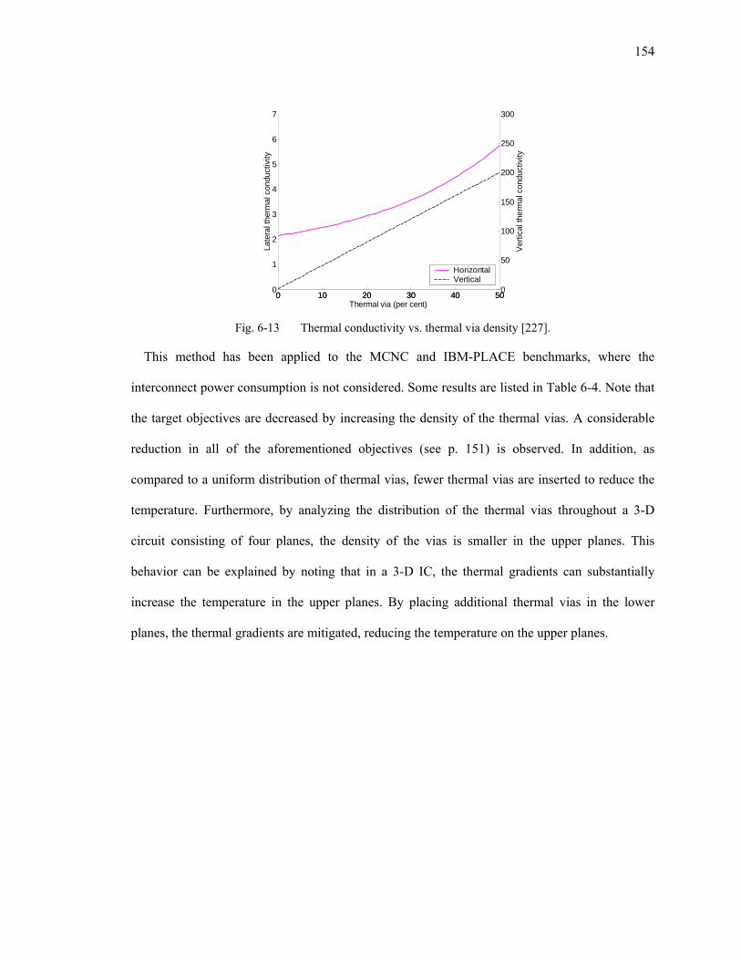
154
0 10 20 30 40 500
1
2
3
4
5
6
7
Late
ral t
herm
al c
ondu
ctiv
ity
Thermal via (per cent)
HorizontalVertical
0 10 20 30 40 500
50
100
150
200
250
300
Ver
tical
ther
mal
con
duct
ivity
Fig. 6-13 Thermal conductivity vs. thermal via density [227].
This method has been applied to the MCNC and IBM-PLACE benchmarks, where the
interconnect power consumption is not considered. Some results are listed in Table 6-4. Note that
the target objectives are decreased by increasing the density of the thermal vias. A considerable
reduction in all of the aforementioned objectives (see p. 151) is observed. In addition, as
compared to a uniform distribution of thermal vias, fewer thermal vias are inserted to reduce the
temperature. Furthermore, by analyzing the distribution of the thermal vias throughout a 3-D
circuit consisting of four planes, the density of the vias is smaller in the upper planes. This
behavior can be explained by noting that in a 3-D IC, the thermal gradients can substantially
increase the temperature in the upper planes. By placing additional thermal vias in the lower
planes, the thermal gradients are mitigated, reducing the temperature on the upper planes.

155
TABLE 6-4 AVERAGE PER CENT CHANGE OF VARIOUS THERMAL OBJECTIVES FOR THE CASE WITH NO
THERMAL VIAS [227].
Objective Average per cent change gmax gave Tmax Tave dthmax dthave
gmax -68.1 -60.8 -44.5 -25.9 44.9 10.2 gave -75.7 -70.7 -51.6 -29.5 50 17.6 Tmax -71.1 -64.5 -47.3 -27.3 50 12.3 Tave -73.2 -67.4 -49.2 -28.3 50 14.3
dthmax -55.5 -43.3 -31.4 -19.2 25 4.2 dthave -79.2 -75.3 -54.7 -31.0 50 23.9
6.3.2. Thermal Via Planning Techniques
Although thermal vias can considerably facilitate the flow of heat towards the ambient, the
placement of the vias can adversely affect other design objectives, such as the area and wirelength
of a 3-D circuit. The density of the thermal vias is, therefore, limited and cannot arbitrarily
increase. Consequently, thermal via planning can be described as the problem of minimizing the
number of thermal vias while the temperature of the circuit and the capacity of the thermal vias
are constrained. Compact thermal models, such as the model described in subsection 6.1.2, are
preferred due to the lower computational time required to obtain the thermal profile of 3-D
circuits as compared to finite element and finite difference methods [217], [228]–[230]. Using as
a baseline the compact thermal model described in subsection 6.1.2, a 3-D circuit is discretized
into tiles. The tiles located on the same x-y coordinates but on different planes constitute a pillar
modeled by a group of serially connected resistors and heat sources (see Fig. 6-6).
Based on this model, the problem of determining the minimum number of through silicon vias
(TSVs) necessary to satisfy a specific temperature constraint can be described by the following
nonlinear programming (NLP) problem,
∑=
n
ithid
2min , (6-24)
where dthi is the thermal TSVs density on plane i for a 3-D circuit comprised of n physical planes.
In addition, a number of constraints apply to (6-24), such as temperature constraints (i.e., the

156
temperature of the circuits cannot exceed a specified value), capacity constraints for the TSVs in
each tile, a lower bound constraint for the number of TSVs such that the wirelength of the circuit
does not increase due to an insufficient number of signal TSVs in a specific tile, and a heat flow
equality constraint (i.e., the incoming and outcoming heat flow for every tile should be equal).
Relating the thermal conductivity of the TSVs with the serially connected resistors in a single
pillar, (6-24) can be rewritten as
∑≥ −
⎟⎟⎠
⎞⎜⎜⎝
⎛−
−2 1,,,,
,,.mink
TSVkjikji
kjivia nTT
IR, (6-25)
where Rvia is the thermal resistance of one TSV [210] and nTSV is the number of TSVs which is
equivalent to the thermal resistance of a tile within a 3-D grid. I and T are the heat flow in the z-
direction and temperature of the tiles in the grid, respectively, and i, j, and k are the index of the
tiles.
Efficiently solving this NLP is a formidable task. Therefore, the thermal via planning process is
divided into a two-stage problem; determining the intraplane thermal TSV density within each
plane of a 3-D circuit and determining the interplane thermal TSV density among the planes
within the stack. Depending upon the formulation of these problems and the applied constraints,
different intraplane and interplane distributions of the thermal TSVs are obtained.
The technique of multilevel routing [230], [231] is extended to 3-D ICs including thermal via
planning. Multilevel routing with thermal via planning can be treated as a three stage process,
illustrated in Fig. 6-14; a coarsening phase, an initial solution generation at the coarsest level of
the grid, and a subsequent refinement process until the finest level of the grid is reached. Before
the coarsening phase is initiated, the routing resources, the capacity of the TSVs, and the power
density in each tile are determined. The power density and routing resources are determined at
each coarsening step. At the coarsest level (level k), an initial routing tree is generated. At this

157
point, the TSV planning step is invoked, assigning TSVs to each tile within a coarse grid. During
the refinement phase, the TSVs are distributed to preserve the solution produced at the previous
level. If the final temperature at the end of the refinement phase does not satisfy a specified
temperature, the TSVs are further adjusted to satisfy the target temperatures.
The TSV planning step is based on the alternating direction TSV planning algorithm (ADVP),
which distributes the TSVs in alternate directions; in the first step, among the planes of the 3-D
IC, and, in the second step, within each plane of the circuit. This algorithm aims at reducing the
overall runtime as the thermal profile required during the various stages of the multilevel routing
process can considerably increase the execution time. The problem of distributing the TSVs
among the planes of the 3-D system can be described as a convex problem. An analytic solution
is determined if the capacity bounds for the TSVs are removed,
∑∑==
−− +=n
kk
n
kknnnnn PPPPPaaaa
2
'
3
''1
''231 :::::::: KK , (6-26)
where ai and Pi’ are, respectively, the number of TSVs and the power density of each tile for a
grid consisting of n planes.
A corresponding analytic solution cannot be easily determined, however, for the horizontal or
intraplane distribution of TSVs. Alternatively, heat propagation and path counting replace the
thermal profiling step. heat propagation considers the propagation of the heat flow among the
tiles of the grid and is determined by evaluating the different paths for transferring heat to the
lower planes of the grid. Different heat propagation paths are illustrated in Fig. 6-15.
The multilevel routing and ADVP algorithm are applied to MCNC benchmarks and compared
both to the TSV-planning approach presented in [228] and to a uniform distribution of TSVs. As
listed in Table 6-5, the ADVP algorithm achieves a significant decrease in the required number of
TSVs in order to maintain the same temperature, possibly resulting in a lower fabrication cost and

158
less routing congestion. From Table 6-5, a considerable reduction in the number of TSVs is
achieved by the ADVP algorithm without any increase in computational time.
Thermal model
1. Power density calculation2. TSV position estimation3. Heat propagation4. Routing resource calculation
1. Power density coarsening2. Routing resource coarsening3. Heat propagation
level 0
level i
level k
level i
level 0
1. Initial tree generation2. ADVP on level k3. TTSV number assignment
1. STSV assignment2. TTSV refinement by ADVP3. TTSV number adjustment4. Routing refinement
Thermal model
Thermal model
1. Power density calculation2. TSV position estimation3. Heat propagation4. Routing resource calculation
1. Power density coarsening2. Routing resource coarsening3. Heat propagation
level 0
level i
level k
level i
level 0
1. Initial tree generation2. ADVP on level k3. TTSV number assignment
1. STSV assignment2. TTSV refinement by ADVP3. TTSV number adjustment4. Routing refinement
Fig. 6-14 Multilevel routing flow with thermal via planning [229].
Ii,j,k
tile i,j,k
Ii,j,k
tile i,j,k
Fig. 6-15 Various heat propagation paths within a 3-D grid [229].

159
TABLE 6-5 COMPARISON OF TSV PLANNING TECHNIQUES.
Circuits m-ADVP [229] m-VPPT [228] Uniform TSV
T [oC] # TSV
Area ratio
Runtime [sec]
T [oC]
# TSV
Area ratio
Runtime [sec]
T [oC]
# TSV Area ratio
Runtime [sec]
ami33 77.0 1282 2.5% 1.55 77.1 1801 3.5% 1.76 77.1 2315 4.5% 1.62 ami49 77.0 20956 0.9% 13.5 77.1 43794 1.8% 12.15 76.9 166366 6.8% 16.17 n100 77.0 11885 1.5% 7.66 77.0 22211 2.8% 8.31 76.8 30853 3.9% 7.54 n200 77.0 13980 1.8% 12.24 77.2 18835 2.4% 10.89 77.1 30346 3.9% 12.21 n300 77.0 17646 1.3% 20.44 77.1 30161 2.2% 21.73 76.9 57342 4.2% 22.42 Avg. 1.0 1.6% 1.0 1.68 2.6% 1.01 3.55 4.6% 1.06
Although the ADVP algorithm reduces the required amount of thermal TSVs, a further
decrease in the density of the thermal TSVs can be achieved by applying a different approach to
determining the TSVs densities. With this approach, both the interplane and intraplane via density
problem is converted to a convex problem through several simplifications [232]. The primary
assumption of this approach is that the silicon substrate of each of the upper physical planes and
the bonding material at the interface between two planes are treated as a single material with
homogeneous material properties. The thickness of this material is the summation of the thickness
of the silicon layer and the bonding layer, with a thermal conductivity Kavg equal to the average
thermal conductivity of the silicon and bonding material. The solution of these convex problems
produces a different distribution of interplane and intraplane TSVs [232], as compared to the
distribution produced by ADVP and a uniform TSV distribution. These differences are
summarized in Table 6-6, where Kvia is the thermal conductivity of the TSVs and S is the area of
the circuit blocks within each plane of a 3-D system.
TABLE 6-6 DIFFERENT SOLUTIONS FOR DISTRIBUTING TSVS IN 3-D ICS.
Algorithm Interplane Planning Intraplane Planning
m-VPPT [228] jithjthi IIdd :: = isikthisthik IIdd :: =
m-ADVP [229] )(,:
SKKaII
dd
avg
viaji
thj
thi ==++
αα
isikthisthik IIdd :: =
TVP [232] 1,:11 −==
++
avg
viaji
thj
thi
KKII
dd λ
λλ
isikthisthik IIdd :: =

160
This modified thermal via planning step has been applied to MCNC and GSRC benchmark
circuits and compared with the ADVP and other TSV distribution algorithms [228], [229]. Some
results are reported in Table 6-7, where the solution of the approximate convex problems reduces
the number of thermal vias required to reach a pre-specified temperature.
TABLE 6-7 COMPARISON AMONG THE REQUIRED NUMBERS OF TSVS.
Circuit m-ADVP [229] m-VPPT [228] TVP [232] Tmax # T-via Tmax # T-via Tmax # T-via
ami33 76.8 1109 76.7 1360 77.5 995 ami49 77.0 21668 77.1 28793 77.2 20310 n100 77.2 16731 76.9 25205 77.0 14533 n200 77.1 14273 76.4 17552 77.1 12869 n300 76.8 19337 76.5 25995 76.9 18614 Avg. 1.12 1.51 1.02
The improved thermal via planning step is integrated into a hierarchical floorplanning
technique [232] for 3-D circuits where the circuit blocks are initially partitioned onto the planes
of the circuit. Since no interplane moves are allowed after the partitioning step is completed, the
partitioning step is crucial in determining the overall quality of the final result. This partitioning
problem is approached as a sequence of knapsack problems [233], where the hottest blocks are
placed on the lower planes of a 3-D circuit to prevent steep thermal gradients as the heat
generated by these blocks is conveyed to the heat sink. Furthermore, overlap (i.e., placement of
the blocks on adjacent physical planes with the same x-y coordinates) among these high power
density blocks is avoided. The integrated thermal via planning and floorplanning approach is
compared with a non-integrated approach, where the floorplan (initially omitting the thermal
objectives) is generated first followed by thermal via planning as a post processing step. The
integrated technique requires 16% fewer thermal vias for the same temperature constraint, with a
21% increase in computational time and an almost 3% reduction in the total area.

161
6.3.3. Thermal Wire Insertion
In addition to the benefits that the added thermal vias produce, thermal wires can also be utilized
to enhance the heat transfer process. These thermal wires correspond to horizontal wires that
connect regions with different thermal via densities through thermal interplane vias. These
thermal wires are treated as routing channels wherever there are available tracks. Both thermal
interplane vias and wires can be handled during routing [234]. Given a placement of cells within
a 3-D IC, the technology parameters, and a temperature constraint, sensitivity analysis and linear
programming methods are utilized to route a circuit. For routing purposes, a 3-D grid is imposed
on a 3-D circuit as shown in Fig. 6-16 for a two plane 3-D circuit. In addition, the thermal model
of the circuit is based on a resistive network, as discussed in subsection 6.1.2. Note that the
interconnect power component is not considered in this thermal model [234].
Placing thermal vias and wires to decrease the circuit temperature adversely affects the
available routing resources while increasing the routing congestion. Each vertical edge of the
routing grid is, therefore, associated with a specific capacity of interplane vias. A similar
constraint applies for the horizontal edges, which represent horizontal routing channels. The
width of the routing channel can be considered equal to the edge width of the tiles. As shown in
Fig. 6-17, the thermal wire and vias affect the routing capacity of each tile.
Fig. 6-16 Routing grid for a two plane 3-D IC. Each horizontal edge of the grid is associated with a
horizontal wire capacity. Each vertical edge is associated with an interplane via capacity.

162
vi
vi
vj
vj
Cell boundaryThermal wires
Interplane vias
Cell i Cell jvi
vi
vj
vj
Cell boundaryThermal wires
Interplane vias
Cell i Cell j
Fig. 6-17 Impact of a thermal wire on the routing capacity of each grid cell. vi and vj denote the capacity
of the interplane vias for cell i and j, respectively. The horizontal cell capacity is equal to the width of the
boundary of the cells [234].
The 3-D global routing flow is depicted in Fig. 6-18 where thermal vias and wires are inserted
to achieve a target temperature under congestion and capacity constraints. A 3-D minimum
Steiner tree is initially generated, followed by an interplane via assignment. A 2-D maze router
produces a thermally driven route within each plane of the circuit. In the following steps [234], an
iterative procedure is applied to insert the thermal vias and wires and complete the physical
routing. A thermal model and sensitivity analysis are used to perform a linear programming based
thermal via and wire insertion in the first step of the iterative procedure. If this insertion violates
the congestion constraints or causes overflow in the routing channels, a rip-up and route step is
used to resolve these conflicts [234]. Thermal profiling and sensitivity analysis are repeated to
determine whether the target temperature has been achieved. The iterations are terminated when
there are no remaining violations or the temperature of the circuit cannot be further improved.
The complexity of the algorithm is bounded by the complexity of the iterative procedure. The
complexity of each iteration is O(NGlogG+G3) where N and G are the number of nets in the
circuit and the number of cells in the routing grid, respectively.

163
3-D MST, routing congestion estimation
Signal interplane via assignment
Evaluating temperature and sensitivity analysis for hot spots
LP-based thermal via and wire insertion
Rip-up and route
Congestion or temperature violations? or temperature
improvement?
Post thermal via and wire insertion
END
NO
YES
3-D MST, routing congestion estimation3-D MST, routing congestion estimation
Signal interplane via assignmentSignal interplane via assignment
Evaluating temperature and sensitivity analysis for hot spots
Evaluating temperature and sensitivity analysis for hot spots
LP-based thermal via and wire insertionLP-based thermal via and wire insertion
Rip-up and routeRip-up and route
Congestion or temperature violations? or temperature
improvement?
Congestion or temperature violations? or temperature
improvement?
Post thermal via and wire insertionPost thermal via and wire insertion
ENDEND
NO
YES
Fig. 6-18 Flowchart of a temperature aware 3-D global routing technique [234].
6.4. Summary
Thermal analysis and related design techniques for 3-D ICs are discussed in this chapter. A
summary of these techniques follows.
• High temperatures deteriorate circuit reliability and lifetime, increase leakage power, and
decrease circuit performance.
• Higher temperatures and thermal gradients are predicted for 3-D ICs due to increased power
densities and greater distances between the circuits on the upper planes and the heat sink.
• Thermal coupling can further increase self-heating of devices, leading to hot spots.
• Thicker silicon substrates facilitate the heat transfer process; however, high aspect ratio
interplane vias reduce the performance of the circuit and are difficult to fabricate.

164
• Thermal models of 3-D circuits includes analytic expressions, compact thermal resistive
networks, and 3-D grids for finite element analysis, in ascending order of increasing
computational complexity and accuracy.
• The increase in temperature of a 3-D circuit exhibits a square and linear relationship with the
number of planes and the power density of each plane, respectively.
• The boundary conditions for the thermal model of a 3-D circuit typically assume adiabatic
walls for the lateral and top surfaces and an isothermal surface for the bottom surface
attached to the heat sink.
• Physical design techniques, such as floorplanning, placement, and routing, that embody a
thermal objective can be a useful tool to manage thermal issues in 3-D ICs.
• Design techniques can reduce thermal gradients and temperatures in 3-D circuits by
redistributing the blocks among and within the planes of a 3-D circuit.
• The thermal-electric duality can be exploited to apply well-established circuit analysis
techniques, such as the application of modified nodal analysis, to thermal design techniques.
• The computational time of the thermal management techniques depends upon the accuracy of
the thermal model. More accurate thermal models achieve improved results but can require
unacceptably high computational times. Alternatively, simpler models reduce runtime but can
provide insufficient accuracy.
• A compromise between the accuracy and the computational requirements of the thermal
model is necessary.
• The heat primarily spreads vertically rather than laterally. Consequently, the thermal
resistance in the horizontal direction can be considered as constant to improve the
computational time for thermal profiling.

165
• The third dimension can greatly affect the computational time by significantly increasing the
solution space of the thermal design techniques.
• Interplane vias that do not carry an electrical signal are called thermal or dummy vias. These
thermal vias can be utilized in 3-D circuits to convey heat to the heat sink.
• Dummy vias create routing obstacles. These vias should therefore be judiciously inserted.
• Thermal via planning describes the problem of minimizing the number of thermal vias while
satisfying temperature and interplane via capacity constraints. Thermal via planning
techniques can significantly decrease the temperature and thermal gradients within a 3-D
circuit.
• Thermal wires in the horizontal direction are equivalent to thermal vias and can be utilized to
lower thermal gradients in 3-D circuits.
166
Chapter 7. Timing Optimization for Two-
Terminal Interconnects
The 3-D interconnect prediction models discussed in Chapter 4 indicate a considerable reduction
in interconnect length for 3-D circuits, which can improve the speed and power characteristics of
modern integrated circuits. In order to exploit this advantage, numerous physical design
techniques for 3-D circuits satisfying a variety of design objectives, such as area, wirelength,
routing congestion, and temperature, have been developed. In addition to this important
advantage, three-dimensional integration demonstrates many opportunities for heterogeneous
SoCs [137].
Integrating circuits from diverse fabrication processes into a single multiplane system can
result, however, in substantially different impedance characteristics for the interconnects of each
physical plane within a 3-D circuit. These particular interconnect traits present new challenges
and opportunities for 3-D circuits. This situation is further complicated by the interplane through
silicon vias which can exhibit different impedance characteristics as compared to the horizontal
(or intraplane), interconnects. By considering the disparate interconnect impedance characteristics
of 3-D circuits, the performance of the interplane interconnects can be significantly improved.
Based on the interconnect prediction models discussed in Chapter 4, these interplane
interconnects are typically the longest lines within a 3-D circuit. Improving the performance of
these global interconnects is therefore of significant importance, since the overall performance of
the system is also significantly enhanced. In this chapter, a technique to decrease the delay of
two-terminal interplane interconnects by optimally placing the interplane vias is described. In the

167
following section, the characteristics of the interplane interconnects, which require a different
interconnect model as compared to 2-D circuits, are discussed.
A closed-form solution for the minimum delay of a two-terminal interplane net that includes
only one interplane via is provided in Section 7.2. The performance degradation that can occur by
not optimally placing the interplane via is also discussed. Two-terminal nets that comprise more
than one interplane via are investigated in Section 7.3. Additionally, an algorithm for placing
interplane vias is described along with simulation and analytic results. A comparison of the
proposed technique with a wire sizing algorithm is also presented. A short summary of the
chapter is presented in the last section.
7.1. Interplane Interconnect Models
The impedance characteristics of the metal layers that belong to different physical planes of a 3-D
circuit can vary significantly. This variation can be attributed to several causes. For example,
consider a 3-D circuit where a processor is integrated with a few memory planes. The fabrication
process used for the processor and the memory plane can result in different impedances among
the metal layers of the bottom and upper planes. In addition, the magnitude of the process
variations, which can affect, for example, the metal layer and inter-layer dielectric thickness, of
each of those processes is different. Consequently, the nominal impedance of the lines in each
plane is affected differently. As a more specific example, consider the fabrication process for 3-D
circuits manufactured by the MITLL [139], [235]. In this process, the third plane of the 3-D
circuit can be optimized for RF circuits. In this case, the resistance of the metal layers in the RF
plane is approximately an order of magnitude lower than that of the metal line resistance in the
other digital planes.

168
If the same manufacturing process, however, is used to fabricate all of the planes of a 3-D
circuit, variations in the impedance characteristics of the lines in a 3-D circuit can also originate
from other causes, such as the bonding style and technology. Consider the interconnect structure,
which is extracted to determine the capacitance on the topmost metal layer, shown in Figs. 7-1a
and 7-1b for a 2-D and 3-C circuit, respectively [236]. In a 2-D circuit, the metal layer located
immediately below the parallel lines is treated as a ground plane. In a 3-D circuit where front-to-
front bonding is employed, the topmost metal layer of the second plane, which is flipped and
bonded onto the first plane, behaves as a second ground plane for the topmost metal layer of the
first physical plane of the 3-D circuit. Alternatively, in the case of front-to-back bonding, a
ground plane can result from the substrate of the second plane if bulk CMOS technology is used
to fabricate the planes of the 3-D circuit. This second ground plane can significantly alter the
capacitance of the interconnects. As an example, consider the MITLL 3-D process, where the 3-D
system is illustrated in Fig. 7-2. In this technology, the lines of the topmost metal layer of the first
and second plane exhibit a different capacitance as compared to the capacitance of the global
metal layer on the third plane.
One ground plane
Two ground planes
(a) (b)
One ground plane
Two ground planes
(a) (b) Fig. 7-1 Global interconnect structures for impedance extraction, (a) three parallel metal lines over a
ground plane in a 2-D circuit and (b) three parallel metal lines sandwiched between two ground planes in a
3-D circuit.
Another important factor in determining the performance of the interplane interconnects is the
impedance characteristics of the interplane vias, which depend upon the bonding style and

169
technology. Front-to-back bonding will likely result in interplane vias with a greater length as
compared to front-to-front bonding since in the latter case the vertical distance among the planes
is greater. Furthermore, the type of technology can have a profound effect on the impedance of
the interplane vias.
BOX
BOXHandle wafer
BOX
1st plane
2st plane
3st plane
BOX
BOXHandle wafer
BOX
BOX
BOXHandle wafer
BOX
1st plane
2st plane
3st plane
Fig. 7-2 A three plane FDSOI 3-D circuit [139], [235]. Planes one and two are front-to-front bonded,
while planes two and three are front-to-back bonded.
To justify this argument, the capacitance of different interplane via structures illustrated in Fig.
7-3 to Fig. 7-5 has been extracted with a commercial impedance extraction tool [238]. The
structure shown in Fig. 7-3 corresponds to that segment of the interplane via that is surrounded by
the horizontal metal levels of a plane within a 3-D system, and is independent of the target
technology (i.e., bulk CMOS or SOI). The number of metal levels surrounding the via, however,
depends upon the fabrication process. Alternatively, the structure shown in Fig. 7-4 corresponds
to an interplane via surrounded by other vias, which traverse the layers of the dielectric and
bonding material (assuming for simplicity to have identical dielectric constants). Such a via
structure can exist in an SOI technology. For 3-D circuits where each plane is fabricated with a
mainstream CMOS processes or with a combination of SOI and CMOS processes, the structure in
Fig. 7-5 can be utilized for capacitance extraction.

170
Fig. 7-3 Capacitance extraction for an interplane via structure; (a) interplane via surrounded by
orthogonal metal layers and (b) capacitance values for various via sizes and spacing values.
Dielec
tric
Interf
ace
s s
s ss
w
Dielec
tric
εd
εi
εd
Dielec
tric
Interf
ace
s s
s ss
w
Dielec
tric
Dielec
tric
Interf
ace
s s
s ss
w
Dielec
tric
εd
εi
εd
(a)
80
180
280
380
480
580
680
500 1000 1500 2000 3000S [nm]
Cvi
a [fF
/mm
]
W = 500 nm W = 1000 nm W = 1750 nm
(b)

171
Fig. 7-4 Capacitance extraction for an interplane via structure; (a) interplane via through layers of
dielectric and the bonding interface, surrounded by eight interplane vias and (b) capacitance values for
various via sizes and spacings. For all of the layers, the same dielectric material is assumed (i.e.,
)2SiOid εεε == .
Local tier
Semiglobal tier
Global tier
Interplane via
s sw
Local tier
Semiglobal tier
Global tier
Interplane via
s sw
(a)
100
150
200
250
300
350
400
450
500
500 1000 1500 2000 3000S [nm]
Cvi
a [fF
/mm
]
W = 500 nm W = 1000 nm W = 1750 nm
(b)

172
Fig. 7-5 Capacitance extraction for an interplane via structure; (a) interplane via through silicon
substrate, surrounded by a thin insulator layer and (b) capacitance values for various via sizes and
thicknesses of the insulator layer.
The interplane interconnects are therefore modeled as an assembly of horizontal interconnect
segments with different impedance characteristics connected by interplane vias. This model is
Sili
con
Inte
rpla
ne v
ia
Insulator
ws
Sili
con
Inte
rpla
ne v
ia
Insulator
Sili
con
Inte
rpla
ne v
ia
Insulator
ws
ws
(a)
0
2
4
6
8
10
12
20 50 100S [nm]
Cvi
a [p
F/m
m]
W = 500 nm W = 1000 nm W = 1750 nm
(b)

173
considerably different from the typical interconnect model used in a 2-D circuit, where a two-
terminal net is modeled by a single segment with the same uniform distributed impedance
throughout the interconnect length. An interplane interconnect connecting two circuits located on
different physical planes is illustrated in Fig. 7-6. In the following sections, it is shown that the
delay of this type of 3-D interconnect can be improved by appropriately placing the interplane
vias.
7.2. Two-Terminal Nets with a Single Interplane Via
In this section, the simple case of an interplane two-terminal net connecting two circuits located
on different physical planes including only one interplane via is considered. The delay model and
the dependence of the delay on the via location are discussed in subsection 7.2.1. A physical
explanation of the variation in delay with the via location is provided in subsection 7.2.2, whereas
the optimum via location for different impedance characteristics of the interconnect segments is
determined in subsection 7.2.3. The improvement in delay for this type of interconnect is
demonstrated in subsection 7.2.4.
7.2.1. Elmore delay model of an interplane interconnect
As previously mentioned, due to the non-uniformity of the interconnects, each segment is
modeled as a distributed RC line with different impedance characteristics, as shown in Fig. 7-6.
The driver is modeled as a step input voltage source with a linear output resistance RS, and the
interconnect is terminated with a capacitive load CL. The total resistance and capacitance of the
horizontal segments 1 and 2 are R1 = r1l1, R2 = r2l2, and C1 = c1l1, C2 = c2l2, where r1, r2, and c1, c2,
denote the resistance and capacitance, respectively, per unit length. The length of the two
horizontal segments is l1 and l2, and the via length is lv1. Since the via may span more than one
physical plane, lv1 can be expressed as

174
( ) vv lnl 11 −= , (7-1)
where n is the number of physical planes among the connected circuits and lv is the length of the
via connecting two metal layers located on two adjacent physical planes. This via length is
determined by the fabrication process and can typically range from 10 µm to 200 µm [38], [106],
[239]. The total length of the line can be expressed as
211 lllL v ++= . (7-2)
rv cvr c r cRS
CLVS
jth Device Plane
ith Device Plane
l
lvl
Lllvl
Driver
Receiver
Fig. 7-6 Two-terminal interplane interconnect with single via and the corresponding electrical model.
Due to the non-uniform impedance characteristics of the line, the via location or, alternatively,
the length of each horizontal wire segment affects the delay of the line. Thus, the objective is to
place the via such that the interconnect delay is minimum. To analyze the delay of a line, the
distributed Elmore delay model has been adopted due to the simplicity and high fidelity of this
model [240]. The accuracy of the model can be further improved as discussed in [241]. However,
unlike a single plane, more than one set of fitting coefficients is required in a 3-D system. The
objective is to determine the via location or, alternatively, the length of segments 1 and 2, such
that the distributed Elmore delay of the line is minimized.
The distributed Elmore delay for the system shown in Fig. 7-6 is

175
( ).)()(
222211112
2211
111
11
RRRRCRRRC
CRRRC
CRRC
CRT
vSLvS
Svvv
Sel
+++++++
+++++= (7-3)
Substituting the total resistance and capacitance with the per unit length parameters, and using (7-
1) and (7-2), the Elmore delay described in (7-3) is a function of the length of the first segment l1,
3122
111 )( AlAlAlTel ++= , (7-4)
where
( ) ( )2221111 221 crcrcrA +−= , (7-5)
( ) ( ) ( ) ( )21222121222111212 )1( rrCcrcrLcrcrcrcrlnccRA Lvvvs −+−+−+−−+−= , (7-6)
( ) ( ) ( )( )( )
( ) .2
)(122
)1(
222
22
2121222
21112
3
crLLcRLrRC
ccRrrCLclncr
crcr
lnA
SSL
vSvLvvvv
v
+++
+−+−+−+⎟⎟⎠
⎞⎜⎜⎝
⎛ +−−= (7-7)
Equation (7-4) describes a parabola, but the convexity is not guaranteed since A1 can be
negative. The second derivative of (7-4) with respect to l1 is
121
2
2Adl
Td el = . (7-8)
Depending upon the sign of A1, the propagation delay of the line exhibits either a minimum or a
maximum as l1 varies or, alternatively, as the location of the via along the line changes. The
following notations are introduced to facilitate the analysis,
1
221 r
rr = , (7-9)
2
112 c
cc = . (7-10)
From (7-9) and (7-10), the second derivative is

176
( )212212121
2
−+= crcrdl
Td el . (7-11)
Since r1c2 is always positive, the sign of (7-11) and, consequently, the timing behavior of the
line only depends upon the sign of the term in the parentheses. For the propagation delay to be
minimum, the following inequality should be satisfied,
021221 >−+ cr . (7-12)
Note that the notations introduced in (7-9) and (7-10) describe resistance and capacitance ratios
and, consequently, are dimensionless. If (7-12) is not satisfied, the delay of the line exhibits a
maximum.
7.2.2. Interplane Interconnect Delay
In the previous subsection, (7-12) only depends on the impedance characteristics of the segments
that constitute the line. The dependence of the delay on the impedance of the segments of the line
is analyzed in this subsection. To better explain this dependence, consider initially an RC
interconnect line of uniform impedance. An optimum wire shaping function of the propagation
delay has been shown to exist for RC interconnects [242]. The optimum wire sizing function is a
monotonically decreasing function of the width as illustrated in Fig. 7-7. This decrease in width
occurs because close to the receiver the downstream capacitance is small and, therefore, this
capacitance is charged by a larger resistance that results from the reduction in line width.
Alternatively, the downstream capacitance close to the driver is large and, consequently, a small
resistance charges the capacitance, due to the widening of the interconnect towards the driver.

177
(a) (b)
(c)
l
(a) (b)
(c)
l
Fig. 7-7 An example of interconnect sizing. (a) An interconnect of minimum width, Wmin, (b) uniform
interconnect sizing W > Wmin, and (c) non-uniform interconnect sizing W = f(l).
An interplane interconnect with non-uniform impedance characteristics can be treated as a
tapered uniform line consisting of only two segments. If r0 and c0 denote the resistance and
capacitance per unit area, respectively, the resistance and capacitance per unit length of the
segments of the interplane interconnect can be described as r1 = r0/w1, r2 = r0/w2, c1 = c0w1, and
c2 = c0w2, where w1 and w2 are the width of the segments of the line. Thus, r21 and c12 characterize
the tapering factor of the line. If r21 > 1 and c12 > 1, the tapering factor is smaller than one and the
delay of the line can be reduced by appropriately selecting the length of the line segments or,
alternatively, the via location. These values of the impedance ratios r21 and c12 correspond to a
decreasing shaping function of the interconnect which decreases the interconnect delay [242].
Consequently, the via location should be selected such that the shape of the interplane
interconnect approaches the sizing function of a uniform interconnect comprised of only two
segments. Note that the optimum placement of the via does not necessarily achieve the optimum
tapering factor as described by the optimum wire sizing function, yet a significant reduction in the
delay of the line is possible. In addition, as discussed in subsection 7.3.3, the optimum via
placement can achieve a greater improvement in delay as compared to wire sizing for interplane
interconnects. This behavior is mainly due to the non-uniform characteristics of the interconnect
and the discontinuities that the interplane vias create in sizing the interconnect.

178
If r21 > 1 and c12 < 1, both the resistance and the capacitance per unit length of segment 2 are
greater than the RC impedance of segment 1 and, typically, the optimum via location is such that
the length of the segment with the higher impedance is minimized. The same relationship applies
to the case where r21 < 1 and c12 > 1. If r21 < 1 and c12 < 1, a longer l1 increases the resistance of
the line, while a longer l2 increases the capacitance of the line. The tapering factor becomes
greater than one and the delay of the line exhibits a maximum. Consequently, the non-uniform
impedance characteristics of the interplane interconnects, which is further enhanced by the
impedance of the interplane vias, does not allow the process of placing a via to be treated as
optimizing a convex function, which has been demonstrated for wire sizing [243]. This argument
is analytically proven in Section 7.3.
7.2.3. Optimum Via Location
In subsection 7.2.1, the timing behavior of the line is shown to depend on the impedance
characteristics of the segments that comprise the line (see expression (7-12)). Placing a via such
that the delay is minimized based on the impedance of the interconnect segments is presented in
this subsection. Note that while the timing behavior of the line with respect to the via location
does not depend on the interconnect length, the via location that achieves the minimum delay
depends upon the interconnect length.
From (7-4) - (7-7), the value of l1 for which the delay exhibits an extremum, either minimum or
maximum, is
( ) ( ) ( ) ( )
⎥⎦
⎤⎢⎣
⎡+−
−+−+−+−+−−−=222111
21222121212221111 2
)1(crcrcr
rrCcrcrLccRcrcrcrcrlnl Lsvvv .(7-13)
Since no constraints have been applied on the value of l1, the extreme point can occur for values
other than within the physical domain of l1, i.e., [ ]rd lll ,1 ∈ where ld = lmin and lr = L-lv1-lmin. lmin

179
determine the minimum distance between a via and a cell, as constrained by the design rules of
the fabrication process. The Lemma in Appendix B characterizes the optimum via location for
various values of r21, c12, and l1.
Depending upon the sign of (7-11) and the value of l1 in (7-13), the optimum via location is
determined for each possible case:
A) 021
2
>dl
Td el . If [ ]rd lll ,1 ∈ , the propagation delay is minimum when l1 is the value described in
(7-13). Consequently, the via should be placed at a distance l1 from the driver. SPICE
measurements of the 50% propagation delay for a 600 µm line are illustrated in Fig. 7-8 versus
the via location l1. Two observations can be made. First, that the delay exhibits a minimum and
that the minima shift to the right as r21 increases. If l1 < ld, the via should be placed closest to the
driver, while if l1 > lr, the via should be placed closest to the receiver.
0.1 0.2 0.3 0.4 0.5 0.628
30
32
34
36
38
40
42
44
46
l1 [mm]
Tel
[p
sec]
r21 = 2 r21 = 2.625 r21 = 3.25 r21 = 3.875 r21 = 4.5
Fig. 7-8 SPICE measurements of 50% propagation delay of a 600 µm line versus the via location l1 for
various values of r21. The interconnect parameters are r1 = 79.5 Ω/mm, rv1 = 5.7 Ω/mm, cv1 = 6 pF/mm, c2 =
439 fF/mm, c12 = 1.45, lv = 20 µm, and n = 2. The driver resistance and load capacitance are RS = 50 Ω and
CL = 50 fF, respectively.

180
B) 021
2
<dl
Td el . In this case, the delay of the line reaches a maximum for the value of l1 as
described in (7-13). If [ ]rd lll ,1 ∈ , according to the Lemma in Appendix B, for l1 < (lr + ld)/2, the
via should be placed closest to the receiver, while for l1 > (lr + ld)/2, the via should be placed
closest to the driver. In Fig. 7-9, SPICE measurements of the 50% propagation delay for a 600
µm line is shown as a function of the via location l1. Note that the delay reaches a maximum and
that the maximum shifts to the right as r21 increases. If l1 < ld, the via should be placed closest to
the receiver, while if l1 > lr, the via should be placed closest to the driver.
0.1 0.2 0.3 0.4 0.5 0.616
17
18
19
20
21
22
l1 [mm]
Tel
[p
sec]
r21 = 0.15 r21 = 0.255 r21 = 0.35 r21 = 0.455 r21 = 0.55 r21 = 0.65
Fig. 7-9 SPICE measurements of the 50% propagation delay for a 600 µm line versus the via location
l1 for various values of r21. The interconnect parameters are r1 = 79.5 Ω/mm, rv1 = 5.7 Ω/mm, cv1 = 6
pF/mm, c2 = 439 fF/mm, c12 = 0.46, lv = 20 µm, and n = 2. The driver resistance and load capacitance are RS
= 50 Ω and CL = 50 fF, respectively.
C) 021
2
=dl
Td el . If the second derivative equals zero, (7-4) becomes
3121 )( AlAlTel += , (7-14)

181
which is a linear function of l1. The first derivative of (7-4) is equal to A2. For A2 < 0, (7-4) is
strictly decreasing, and the delay is minimum by placing the via closest to the receiver. For A2 >
0, (7-4) is strictly increasing, and the delay is minimum by placing the via closest to the driver.
Note that the fundamental minimum distance of a via from a cell is technology dependent. In the
special case where r21 = c12 = 1, from (7-6) and (7-7), A2 << A3 and the delay is independent of l1.
However, as n increases, A2 also increases and the choice of n affects the rate of change in the
delay. This particular case corresponds to the model introduced in [129] to evaluate the
performance of 3-D ICs, which does not capture the timing behavior of interplane interconnects
in 3-D circuits as analyzed in cases A and B.
As illustrated in Figs. 7-8 and 7–9, the optimum via location shifts to the right (left) when r21
increases (decreases). To explain this behavior, consider the definitions of r21 and c12 in (7-9) and
(7-10), where r21 (c12) describes the resistance (capacitance) ratio of the corresponding horizontal
segments. Referring to Fig. 7-8, both r21 and c12 are greater than one, which means that segment 1
is less (more) resistive (capacitive) than segment 2. Assuming that r21 = 1, the delay of the line
decreases as the length of the more capacitive segment l1 (i.e., C1) decreases. However, l1 does
not vanish because C2 increases as l1 decreases, approaching C1. Consequently, as l1 is decreased
beyond a certain distance, described in (7-13), the delay starts to increase. As r21 becomes greater
than one, the optimum point occurs with increasing values of l1, although segment 1 is more
capacitive than segment 2 (c12 > 1). This behavior occurs because the delay depends not only on
the capacitance, but also on the current, which is controlled by the resistance of each segment.
Due to the distributed nature of the impedance of the line, an increase in the resistance of the
second segment (increasing r21) can be compensated, such that the delay remains minimum, by
reducing the capacitance that this resistance sees near the receiver (the upstream resistance). In
the case where c12 >> 1 and r12 << 1, and where segment 1 is both more capacitive and resistive

182
than segment 2, l1 becomes small to reduce the overall delay. In this case, (7-13) yields negative
values for l1 and is essentially zero (the via should be located next to the driver).
7.2.4. Improvement in Interconnect Delay
SPICE simulations of the 50% propagation delay of two-terminal nets with a single via are listed
in Table 7-1 for various impedance characteristics. The interconnect propagation delay listed in
columns 8, 9, and 11 corresponds to the cases where the via is optimally placed, the via is placed
at the center of the interconnect, and at the maximum delay point. In column 10, the improvement
in delay over the case where the via is placed at the center of the line is reported, while the
improvement in delay over placing the via at the endpoints of the line is listed in column 12. If
the delay exhibits a minimum according to (7-11), the maximum delay point coincides with one
of the endpoints of the interconnect, otherwise the maximum delay point is described by (7-13).
The delay analysis considers relatively short interconnect lengths where repeaters cannot reduce
the interconnect delay, and therefore optimally placing the vias is the primary way to decrease the
delay of such interconnects.
TABLE 7-1 SPICE SIMULATION RESULTS FOR TWO-TERMINAL INTERCONNECTS WITH A SINGLE
INTERPLANE VIA.
Length [µm] RS [Ω] CL [fF] r1 [Ω/mm] c2 [fF/mm] r21 c12 Topt Tcenter Impr [%] Tmax Impr [%]200 100 50 159.5 239 3.50 1.55 19.79 20.02 1.16 20.76 4.90 200 100 50 159.5 239 2.85 1.85 19.89 20.08 0.96 20.44 2.77 300 120 100 93.8 387 2.88 1.67 36.03 36.30 0.75 37.62 4.41 300 120 100 93.8 387 2.88 1.35 34.56 34.80 0.69 35.92 3.94 400 100 100 75.8 287 2.15 2.87 29.30 34.98 19.39 42.34 44.51 400 100 100 75.8 287 3.70 0.77 24.74 28.94 16.98 33.34 34.76 500 30 100 23.8 287 1.50 2.57 54.02 63.37 17.31 72.58 34.36 500 30 100 23.8 287 3.35 2.37 58.18 58.69 0.88 59.77 2.73 500 30 100 23.8 287 3.15 0.87 51.09 54.83 7.32 59.02 15.52
Average Improvement 7.27 16.43
Note that the improvement in delay achieved by optimally placing the via is considerable for
those cases where the optimum location coincides with the endpoints of the interconnect. This
large improvement occurs because in these cases the minimum delay point as described by (7-13)

183
occurs at values between the endpoints of the interconnect, i.e., [0, L]. For these instances, the
propagation delay has an almost linear dependence (with large slope) on the via location and,
therefore, the improvement in delay is significant. Alternatively, for those instances where the
optimum occurs for positive values smaller than the interconnect length L, the variation in the
delay improvement is small as the delay exhibits a parabolic form, and consequently the rate of
change in the delay with via location is small.
For several interconnect instances the optimum location is either close to the receiver or the
driver. Routing congestion therefore causes some of the interplane vias to be placed at non-
optimal locations. In addition, the improvement in delay that can be achieved varies considerably
with the interconnect parameters. In Figs. 7–10 and 7–11, the decrease in the improvement in
delay resulting from the non-optimal placement of the vias is illustrated for a 500 µm interplane
interconnect. The ratios r21 and c12 range from 0.1 to 5 and the interplane via is placed 50 µm
from the optimum location.
A non-negligible reduction in the improvement in delay can occur from the non-optimal
placement of the via for a 50 µm departure from the optimal location. In addition, the decrease in
improvement is greater for those values of r21 and c12, where the optimum is at the endpoints of
the line. For the optimum location corresponding to points along the interconnect length, the
decrease in the delay improvement is small as depicted by the approximately flat portion of the
surface in Figs. 7-10 and 7-11. In addition, the dependence of the delay improvement on the
capacitance ratio c12 is in general greater than the dependence on the resistance ratio r12. For low
values of the driver resistance, the dependence of the delay improvement on r12 is significant, as
shown in Fig. 7-10. Increasing the driver resistance lowers this dependence as depicted in Fig.
7-11, as the term ∑i
iS CR dominates the delay of the line.

184
Fig. 7-10 Decrease in the delay improvement caused by the non-optimal placement of the interplane via
for a 500 µm interconnect. The interconnect parameters are r1 = 23.5 Ω/mm, rv1 = 270 Ω/mm, cv1 = 270
fF/mm, c2 = 287 fF/mm, lv = 15 µm, and n = 2. The driver resistance and load capacitance are RS = 30 Ω
and CL = 100 fF, respectively.
This dependence shows that for large drivers, even if the interconnect is almost uniform (r21 ≈
1), considerable savings in delay can be achieved by optimally placing the via. Furthermore, as
larger drivers are used to reduce the interconnect delay, the improvement in delay becomes
greater. If small drivers are utilized, the savings in delay is primarily obtained from the difference
in the capacitance of the segments, even if c12 ≈ 1. Additionally, a slight decrease in the
maximum degradation of the improvement in delay that occurs from a non-optimal via placement
can be observed in Figs. 7–9 and 7-10. This decrease occurs due to the increase in the driver
resistance, which is considered fixed and can greatly affect the interconnect delay, while the delay
variation due to the impedance characteristics of the segments is reduced. A similar behavior
applies for the capacitance ratio c12 where the load capacitance is increased. In the following
section, two-terminal nets with multiple interplane vias are investigated.

185
Fig. 7-11 Decrease in the delay improvement due to the non-optimal placement of the interplane via for
a 500 µm interconnect. The interconnect parameters are r1 = 23.5 Ω/mm, rv1 = 6.7 Ω/mm, cv1 = 270 fF/mm,
c2 = 287 fF/mm, lv = 15 µm, and n = 2. The driver resistance and load capacitance are RS = 100 Ω and CL =
100 fF, respectively.
7.3. Two-Terminal Interconnects with Multiple Interplane Vias
In the previous section, the case where a two-terminal interconnect includes only one interplane
via is analyzed. Due to routing obstacles and placed cells, however, a stacked interplane via that
spans multiple physical planes may not be possible. In addition, in the previous analysis, no
constraints on the location of the via is imposed. This situation is rather impractical since existing
interconnects and active devices may not permit an interplane via to be placed at a particular
location along the interconnect line. In addition, since these vias penetrate the device layers,
certain regions are reserved for interplane via placement to minimally disrupt the location of the
transistors.

186
Due to these reasons, a two terminal interplane interconnect in a 3-D circuit consists of
multiple interplane vias where each one of these vias is placed within a certain physical interval.
A schematic of an interplane interconnect connecting two circuits located n planes apart is
illustrated in Fig. 7-12. The horizontal segments of the line are connected through the vias, which
can traverse more than one plane. Consequently, the number of horizontal segments within the
interconnect m is smaller or at most equal to the number of physical planes between the two
circuits, i.e. n ≥ m, where the equality only applies when each of the vias connects metal layers
from two adjacent physical planes.
Each horizontal segment j of a line is located on a different physical plane with length lj. The
vias are denoted by the index of the first of the two connected segments. For example, if a via
connects segment j and j+1, the via is denoted as vj with length lvj. Note that planes j and j+1 are
not necessarily physically adjacent. The total length of the line L is equal to the summation of the
length of the horizontal segments and vias,
nvjjv lllllL ++++++= ......11 . (7-15)
The length of each horizontal segment of a line is bounded,
1,minmin =∆+≤≤ jforxlll jjjj , (7-16a)
]1,2[min1min −∈∆++∆≤≤ − mjforxlxll jjjjj , (7-16b)
mjforxlll jjjj =∆+≤≤ − ,1minmin , (7-16c)
and the via placement is also constrained,
jj xx ∆≤≤0 , (7-17)
where ljmin denotes the minimum length of the interconnect segment on plane j, and ∆xj is the
length of the interval in where the via that connects planes j and j+1 is placed. This interval

187
length is called the “allowed interval” here for clarity. xj is the distance of the via location from
the edge of the allowed interval.
liminlvi
lvj
ljmin
∆xi
∆xj
Ruj
Cdj
lkmin
lvk
n pl
anes
l lv L lljlvjlklvkln
lnlm
lm
Fig. 7-12 Interplane interconnect consisting of m segments connecting two circuits located n planes
apart.
ljmin is the length of an interconnect segment connecting two allowed intervals or an allowed
interval and a placed cell. These lengths are considered fixed. Alternatively, the routing path of a
net is not altered except for the via location within the allowed interval. Each horizontal segment
is assumed to be on a single metal layer within the physical plane. In the case where a horizontal
segment is on more than one layer, as the outcome of a layer assignment algorithm [244], the
problem can be approached in two different ways. The intraplane vias can be treated as additional
variables where the location of these vias needs to be determined. This formulation requires,
however, the generation of additional allowed intervals, specifically for the intraplane vias.
Alternatively, the first and last section of the segment connected to the interplane vias remains as
a variable while the remaining sections of the horizontal segment constitute the minimum length
of segment ljmin, which is constant.

188
The distributed Elmore delay model is used to determine the delay of these interconnects and
the corresponding electrical model of the line is depicted in Fig. 7-13. The related notation is
listed in Table 7-2. The distributed Elmore delay of a two-terminal interconnect in matrix form is
DT ++= blAlll T5.0)( , (7-18)
[ ]Tl mm llll 121 −= L , (7-19)
⎥⎥⎥
⎦
⎤
⎢⎢⎢
⎣
⎡=
mmmm
m
crcrcr
crcrcr
L
MLMM
L
21
12111
A , (7-20)
T
b
⎥⎥⎥⎥⎥
⎦
⎤
⎢⎢⎢⎢⎢
⎣
⎡
⎟⎠⎞
⎜⎝⎛ ++
+⎟⎠⎞
⎜⎝⎛ +
=
∑
∑
−
=
−
=
1
1
1
1
11
m
iviviSmLm
SL
m
ivivi
lrRcCr
RcClcr
M , (7-21)
∑∑∑−
=
−
=
−
=+++=
1
1
21
1
1
1 21 m
iLSvivi
m
iviviL
m
iviviS CRlcrlrClcRD
vi. (7-22)
Since (7-22) is a constant quantity, the optimization problem can be described as follows,
(P) minimize blAlll T += 5.0)(T ,
subject to (7-15) - (7-17).
TABLE 7-2 NOTATION FOR TWO-TERMINAL INTERPLANE INTERCONNECTS.
Notation Definition RS Driver resistance CL Load capacitance
rj (cj) Resistance (capacitance) per unit length of horizontal segment j rvj (cvj) Resistance (capacitance) per unit length of interplane via vj Rj (Cj) Total interconnect resistance (capacitance) of horizontal segment j
Rvj (Cvj) Total interconnect resistance (capacitance) of interplane via vj
juR Upstream resistance of the allowed interval for via vj
jdC Downstream capacitance of the allowed interval for via vj

189
As described by the following theorem, the primal problem (P) is typically not convex and
therefore convex quadratic programming optimization techniques are not directly applicable.
Theorem 1: The primal optimization problem (P) is convex iff
11 ++ − jjjj crcr > 0. (7-23)
Proof: A is a positive definite matrix if all subdeterminants are positive. By elementary row
operations, the subdeterminants of A are positive iff (7-23) applies. If (7-23) applies, A is positive
definite and (P) is a convex optimization problem.
Note that condition (7-23) must be satisfied for every segment j such that (P) is a convex
optimization problem. Due to the heterogeneity of 3-D circuits, (7-18) typically is of indefinite
quadratic form. Therefore, convex quadratic programming techniques may not produce the global
minima. Certain transformations can be applied to convert (P) into a convex optimization
problem [245]; the objective functions, however, are no longer quadratic. Alternatively, (P) can
be treated as a geometric programming problem. Geometric programs include optimization
problems for functions and inequalities of the following form,
njjj an
M
j
aaj yyysg ∑
==
121
21)( Ly , (7-24)
12121 ≤njjj a
naa
j yyys L , (7-25)
where the variables yj’s and coefficients sj’s must be positive and the exponents aij’s are real
numbers. Although equality constraints are not allowed in standard geometric problems, (P) can
be solved as a generalized geometric program as described in [246] where a globally optimum
solution is determined. Alternatively, by considering the particular characteristics of the
optimization problem, an efficient heuristic is proposed for placing the interplane vias.

190
rv cvr c ri ci rvi cvi rn cnRS
CLVS
Fig. 7-13 Interplane interconnect model composed of a set of non-uniform distributed RC segments.
7.3.1. Two-Terminal Via Placement Heuristic
In this section, a heuristic for the near-optimal interplane via placement of two-terminal nets that
include several interplane vias is described. The key concept in the heuristic is that the optimum
via placement depends primarily upon the size of the allowed interval (that is estimated or known
after an initial placement) rather than the exact location of the via. Consider the interplane
interconnect line shown in Fig. 7-12, where the optimum location for via j connecting
interconnect segments j and j+1 is to be determined. With respect to this via, the critical point
(i.e., 0=∂∂
j
el
xT
) of the Elmore delay is
( ) ( ) ( ) ( )⎥⎥⎦
⎤
⎢⎢⎣
⎡
+−−+−∆+−+−+−
−=+++
++++++++
111
11111111
2 jjjjjj
jjdjjjjjjjujjjjjjvjvjjvjj crcrcr
rrCcrrxccRcrcrcrcrlx ,(7-26)
where Ruj and Cdj are the upstream resistance and downstream capacitance, respectively, of the
allowed interval for via j (see also Table 7-2), as shown in Fig. 7-12. The Elmore delay of the line
with respect to xj can be either a convex or a concave function. The remaining discussion in this
section applies to the case where the Elmore delay of the line is a convex function with respect to
xj. A similar analysis can be applied for the concave case.
In (7-26), the optimum via location xj* is a monotonic function of Ruj and Cdj. The sign of the
monotonicity depends upon the interconnect impedance parameters of the segments j and j+1
connected by via j. As the size of the allowed intervals for all of the vias is constrained by (7-17),
the minimum and maximum value of Ruj and Cdj can be readily determined, permitting the values

191
of xj* for these extrema, *
minjx and ,*maxjx to be evaluated. Due to the monotonic dependence of xj
on Ruj and Cdj, the optimum location for via j, xj*, lies within the range delimited by *
minjx and
.*maxjx The following four cases can be distinguished,
(i) if *maxjx ≤ 0, xj
*= 0, and the optimum via location coincides with the lower bound of
the interval as defined by (7-17).
(ii) if *minjx ≥ ∆xj, xj
* = ∆xj, and the optimum via location coincides with the upper bound
of the interval as defined by (7-17).
(iii) if ∆xj ≥ *minjx ≥ 0 and ∆xj ≥ *
maxjx ≥ 0, the bounded interval as defined by (7-17)
reduces to
jjjj xxxx ∆≤≤≤≤ *max
*min0 . (7-27)
In this case, the via location cannot be directly determined. However, by iteratively decreasing
the range of values for xj*, the optimal location for via j can be determined.
The following example is used to demonstrate that the physical domain for xj* iteratively
decreases to a single point, the optimum via location. A detailed analysis of the heuristic is
provided in Appendix C. Consider segments i, j, and k depicted in Fig. 7-12, where segments i
and k are located upstream and downstream of segment j, respectively. From (7-16) and (7-17),
the minimum and maximum values of Rui0, Ruj
0, Ruk0, Cdi
0, Cdj0, and Cdk
0 are determined, where the
superscript represents the number of iterations. Assume that 0*minx and 0*
maxx are obtained from (7-
26) to satisfy (7-27) for all of three segments i, j, and k. As the range of values for the via location
of segments i and k decreases according to (7-27), the minimum (maximum) value of the
upstream resistance and downstream capacitance of segment j increases (decreases), i.e.,
,1min
0min ujuj RR < ,1
min0
min djdj CC < ,0max
1max ujuj RR < and .0
max1
max djdj CC < Due to the monotonicity of xj*

192
on Ruj and Cdj, 1*min
0*min jj xx < and .0*
max1*max jj xx < The range of values for xj
* therefore also decreases
and, typically, after two or three iterations, the optimum location for the corresponding via is
determined. In Fig. 7-14, the convergence of the heuristic at the optimum via location is depicted
for one via of a two-terminal interconnect. For this example, cj > cj+1 and rj > rj+1, and, therefore,
),( minmin*
min jjj CRfx = and ),( maxmax*
max jjj CRfx = . As shown in Fig. 7-14, the heuristic
converges to the optimum via location within several iterations.
0 1 2 3 4 50.08
0.09
0.1
0.11
0.12
0.13
0.14
0.15
0.16
0.17
Line length [length units]
Line
del
ay [t
ime
units
]
x*0jmax = f(R0
ujmax,C0djmax)
x*1jmax = f(R1
ujmax,C1djmax)
x*0jmin = f(R0
ujmin,C0djmin)
x*1jmin = f(R1
ujmin,C1djmin)
x*2jmin = x*2
jmax = x*j
Fig. 7-14 Case (iii) of the two-terminal net heuristic. The allowed interval is iteratively decreased such
that the optimum via location is eventually determined.
(iv) if *minjx ≤ 0 and *
maxjx ≥ ∆xj, the via location cannot be directly determined. Additionally,
the bounding interval cannot be reduced. Consequently, some loss of optimality occurs. This
departure from the optimal, however, is typically smaller than a few per cent for all of the
tested conditions as shown by the results presented in subsection 7.3.3.
The variation between the extrema of the upstream resistance and downstream capacitance due
to the relatively small size of the allowed interval of the via placement ensures that a significant
variation between the values *minjx and *
maxjx does not occur for most interconnects. To justify

193
this argument, the extreme values of xj* are plotted in Fig. 7-15 for the fourth interplane via of a
two-terminal net considered to traverse eight planes. This example represents a significant
variation in the extreme values of xj*, due to the location of the via and the large number of vias
along the interconnect. Indeed, the large number of vias (seven in this example) implies a
considerable variation in the value of the downstream capacitance and upstream resistance,
particularly for the fourth via. Note that the last via of the interconnect, for instance, only sees a
variation in the upstream resistance. As shown in Fig. 7-15, less than 1% of the interconnect
instances yield such boundary values for xj* such that the inequalities *
minjx ≤ 0 and *maxjx ≥ ∆xj
are satisfied. This small per cent (1% in this case) is similar or smaller for the other vias of the
interconnect due to the smaller variation in the upstream resistance or downstream capacitance. In
addition, the inequalities, *minjx ≤ 0 and *
maxjx ≥ ∆xj, are typically satisfied, where the size of the
allowed interval for a via is relatively small as compared to the size of the allowed intervals for
the remaining vias. A non-optimal via placement for that interconnect segment does not
significantly affect the overall delay of the line.
Furthermore, for case (iv) to occur, there should be at least two vias for which an optimum
location cannot be found. Indeed, if all but one of the vias are placed, the exact value of the
upstream (downstream) resistance (capacitance) for the non-optimized via can be obtained and,
therefore, the location of that via can be determined from (7-26). The non-optimal placement of a
via does not necessarily affect the optimal placement of the remaining vias. For example, any via
placed according to the criteria described in (i) and (ii) is not affected by the placement of the
remaining vias. Therefore, as noted earlier, the size of the allowed intervals rather than the exact
location of the vias is the key factor in determining the optimum via locations. Based on this
heuristic, an algorithm for placing a via in two-terminal nets is presented in the following
subsection, along with simulation and analytic results for such interconnects.

194
500 1000 1500 2000 2500 3000-200
-150
-100
-50
0
50
100
150
200
Interconnect instances
x* jm
in/m
ax[µ
m]
x*jmin < 0
x*
jmax > ∆xj
Fig. 7-15 A subset of interconnect instances depicted by the dashed lines for case (iv) of the via
placement heuristic. The interconnect traverses eight planes and has a length L = 1.455 mm. The resistance
rj and capacitance cj of each interconnect segment range from 10 Ω/mm to 50 Ω/mm and 100 fF/mm to 500
fF/mm, respectively.
7.3.2. Two-Terminal Via Placement Algorithm
The heuristic described in the previous subsection has been used to implement an algorithm that
exhibits an optimal or near-optimal via placement for two-terminal interplane interconnects in 3-
D ICs, with significantly lower computational time as compared to geometric programming
solvers. The pseudocode of the two-terminal via placement algorithm (TTVPA) is illustrated in
Fig. 7-16. The input to the algorithm is a description of the interplane interconnect where the
minimum length of the segments and the size of the allowed intervals are provided. In the first
step of the algorithm, the array of the maximum and minimum upstream (downstream) resistance
(capacitance) for every allowed interval is determined. In the following steps, for each
unprocessed via, the range of values for the optimum via location as given by (7-26) is evaluated.
In step five, these values are compared to the inequalities described in the previous subsection. If
an optimal via location is determined in this step, the via is marked as processed and the

195
capacitance and resistance arrays are updated. If, after a number of iterations, there are non-
optimal vias, in step 14 these vias are placed at the center of the corresponding allowed intervals
and the algorithm terminates. Other criteria, such as routing congestion, can alternatively be
applied to place non-optimal vias rather than placing these vias at the center of the corresponding
allowed intervals. Further criteria can be considered to search for the optimum location of the
non-optimal vias, trading off runtime with accuracy.
Fig. 7-16 Pseudocode of the proposed Two-Terminal Net Via Placement Algorithm (TTVPA).
7.3.3. Application of the Via Placement Technique
The via placement algorithm has been applied to several interconnect instances to validate the
accuracy and efficiency of the heuristic. Both SPICE simulations and optimization results are
provided. Two-terminal interplane interconnects for different numbers of physical planes are
analyzed. The impedance characteristics of the horizontal segments and vias are extracted for
several interconnect structures using a commercial impedance extraction tool [238]. Copper
interconnect has been assumed with an effective resistivity of 2.2 µΩ-cm. Based on the extracted
impedances, the resistance and capacitance of the horizontal segments range from 25 Ω/mm to
Two-Terminal Via Placement Algorithm: (lmin,∆x) 1. Determine Cdmin, Cdmax, Rumin, Rumax 2. while S ≠ Ø 3 if iter < max_iter 4. sj ← an unprocessed via
5. obtain *minjx and *
maxjx from eq. (7-26)
6. check for the inequalities in (i) – (iv) 7. if sj is optimized (cases i-ii) 8. store optimum via location 9. S ← S – sj
10. update Cdmin, Cdmax, Rumin, Rumax elseif ∆xj decreases (case iii)
11. update lminj, Cdmin, Cdmax, Rumin, Rumax else (case iv)
12. go to step 3 else (the non-optimized vias)
13. place via at the center of the allowed interval 14. store via location 15. S ← S – sj
16. exit

196
125 Ω/mm and 100 fF/mm to 300 fF/mm, respectively, for a 90 nm technology node [247], [248].
The cross section of the vias is 1 µm × 1 µm, with 1 µm spacing from the surrounding horizontal
metal layers assuming, a silicon on insulator (SOI) process as described in [139]. For all of the
interconnect structures, the total and minimum length of each horizontal segment is randomly
generated. For simplicity, all of the vias connect the segments of two adjacent physical planes
(i.e., m = n).
Delay simulations are reported in Table 7-3. The delay of the line Tcenter, where the vias are
placed at the center of the allowed intervals, is listed in column 2. The delay Trnd, listed in column
3, corresponds to the line delay for random via placement. The minimum interconnect delay Tmin,
where the vias are optimally placed, is listed in column 4. The via locations or, equivalently, the
length of the horizontal segments, are determined from the via placement algorithm. The
improvement in delay as compared to the case where the vias are placed at the center of the line is
listed in column 5. The number in parentheses corresponds to the improvement in delay over a
random via placement. Note that the variation in the improvement in delay changes significantly
for those listed instances, although the interconnect lengths are similar and the load capacitance
and driver resistance are the same. This considerable variation demonstrates the strong
dependence of the line delay on the impedance characteristics of the segments of the line and
supports modeling the interplane interconnect as a group of non-uniform segments. Additionally,
depending upon the impedance characteristics of the line segments, placing a via at the center of
the allowed intervals is, for certain instances, near-optimal, explaining why the improvement in
delay is not significant in these instances. The same characteristic applies to those cases where a
random placement is close to the optimum placement. Nevertheless, as listed in Table 7-3, an
improvement of up to 32% is observed for relatively short interconnects, demonstrating that an

197
optimum via placement can significantly enhance the speed of 3-D circuits (in addition to the
primary benefit of reduced wire length and therefore lower power).
TABLE 7-3 SPICE SIMULATION RESULTS DEMONSTRATING THE DELAY SAVINGS ACHIEVED BY NEAR
OPTIMAL VIA PLACEMENT. THE RESISTANCE AND CAPACITANCE PER UNIT LENGTH OF THE VIAS ARE rvi = 6.7
Ω/mm AND cvi = 6 pF/mm, RESPECTIVELY. THE LENGTH OF THE VIAS IS lvi = 20 µm. THE DRIVER RESISTANCE
IS Rs = 15 Ω AND THE LOAD CAPACITANCE IS CL = 100 fF. THE LENGTH OF THE ALLOWED INTERVALS IS ∆xi =
200 µm.
Length [µm] Tcenter [ps] Trnd [ps] Tmin [ps] Improvement [%] n
1017 12.35 12.64 11.42 8.14 (10.68) 4 1180 13.37 14.42 12.33 8.43 (16.95) 4 849 11.00 11.71 10.27 7.11 (14.02) 4 969 13.52 14.96 12.12 11.55 (23.43) 4 967 12.38 12.59 11.72 5.63 (7.42) 4 1612 18.54 19.85 17.24 7.54 (15.14) 5 1537 20.80 19.47 19.37 7.38 (0.52) 5 1289 17.78 18.43 16.45 8.09 (12.04) 5 1443 18.77 19.54 18.07 3.87 (8.14) 5 1225 16.97 18.33 15.62 8.64 (17.35) 5 2118 30.52 34.81 26.44 15.43 (31.66) 7 2130 27.92 27.32 25.94 7.63 (5.32) 7 1961 28.49 30.67 26.16 8.91 (17.24) 7 2263 35.58 40.11 31.31 13.64 (28.11) 7 2174 32.31 30.34 29.16 10.80 (4.05) 7
Average Improvement 8.85 (14.14)
The two-terminal via placement algorithm is compared both in terms of optimality and
efficiency to two optimization solvers. The first solver, YALMIP [249], is a general optimization
solver that supports geometric programming while GLOPTIPOLY [250] is an optimization solver
for non-convex polynomial functions. Due to the excessive computational time of GLOPTIPOLY
(greater than three orders of magnitude slower than YALMIP), only comparisons with YALMIP
are reported. Optimization results are listed in Table 7-4 for different values of ∆x ranging from
50 µm to 300 µm.
As reported in column 9 of Table 7-4, TTVPA exhibits high accuracy as compared to
YALMIP. These results are independent of the number of planes that comprise the 3-D
interconnect, demonstrating that TTVPA yields optimum solutions for most interconnect
instances. In addition, for those cases where some of the vias are not optimally placed, the loss of

198
optimality is insignificant (as previously discussed). In column 8, the runtime ratio of YALMIP to
TTVPA is listed. TTVPA is approximately two orders of magnitude faster than YALMIP. The
complexity of TTVPA has an almost linear dependence on the number of interplane vias. As
depicted in Fig. 7-16, each via is typically processed once; otherwise, a maximum of two to five
iterations is required to place a via. In all of the experiments, the algorithm terminates within a
number of iterations smaller than five times the total number of vias within the interconnect.
TABLE 7-4 OPTIMIZATION RESULTS FOR VARIOUS TWO-TERMINAL INTERPLANE INTERCONNECTS AND
NUMBERS OF PHYSICAL PLANES n.
n Average
Interconnect Length [µm]
∆xi’s [µm]
Delay Improvement [%] YALMIP/TTVPA Runtime ratio
× times
Max. error [%] InstancesVias placed at the center Random via placement
Avg Max Avg Max 3 270 50 3.36 11.10 5.88 22.24 141.7 0.005 10000 3 520 100 4.59 17.63 5.02 17.63 148.6 0.008 10000 3 1020 200 5.90 23.12 10.27 47.08 145.6 0.013 10000 4 405 50 4.02 13.01 6.00 25.97 209.4 0.006 10000 4 781 100 5.26 16.95 7.91 34.10 574.3 0.003 10000 4 996 100 3.45 9.87 5.37 20.05 95.5 0.008 5000 4 1155 150 5.94 21.61 8.89 44.46 125.4 0.011 10000 4 1302 200 6.31 22.76 9.87 46.91 241.6 0.021 5000 4 1600 300 8.73 26.85 12.58 55.91 111.4 0.025 5000 5 540 50 4.48 13.73 6.16 27.49 112.14 0.005 10000 5 1040 100 5.69 17.97 7.79 35.82 335.40 0.012 10000 5 1541 150 6.35 22.36 8.63 46.26 549.35 0.017 10000 5 1277 100 3.91 10.84 5.57 22.04 93.1 0.003 5000 5 1684 200 7.06 19.65 10.09 41.28 226.4 0.009 5000 5 2076 300 9.77 26.74 14.27 55.45 90.1 0.009 5000 7 1840 100 4.64 12.81 6.21 25.16 84.6 0.008 5000 7 2440 200 8.26 23.77 11.07 47.56 89.0 0.002 5000
As shown in Table 7-4, the savings in delay from the near-optimal via placement strongly
depends upon the length of the allowed intervals. For example, doubling the length of the allowed
intervals for via placement increases almost twofold the maximum improvement in delay. As the
length of the allowed intervals increases, the constraints in (7-16) are relaxed and a greater benefit
from optimally placing the vias is achieved.
The effect of the non-uniformity of the interplane interconnects on the improvement in delay is
graphically illustrated in Fig. 7-17, where the improvement in delay for interplane interconnects
spanning four and five physical planes is depicted. The average savings in delay of highly non-

199
uniform interconnects (i.e., r(j+1) / rj = 1 – 10 and cj / c(j+1) = 1 – 10) can be significant,
approaching 10% and 13% for a moderately sized length, where the vias are placed at the center
of the allowed intervals and are randomly placed, respectively. The maximum improvement can
exceed 60%, as shown in Fig. 7-17.
Avg.Avg.
Avg.Max.
Max.
Max.
Avg.
Avg.
Avg.
Max.
Max.
Max.
Avg.Avg.
Avg.
Max.
Max.
Max.
Avg.
Avg.
Avg.
Max.
Max.
Max.
0
10
20
30
40
50
60
70
1-3 1-5 1-10
Ratio of interconnect segment impedances
Impr
rove
men
t in
dela
y [%
]
n = 4, Via placement at the centern = 4, Via placement at the centern = 4, Random via placementn = 4, Random via placementn = 5, Via placement at the centern = 5, Via placement at the centern = 5, Random via placementn = 5, Random via placement
Fig. 7-17 Average and maximum improvement in delay for different range of interconnect segment
resistance and capacitance ratios. (a) The vias are placed at the center of the allowed intervals and (b) the
vias are randomly placed.
The length of most of the interconnects listed in Tables 7-1 to 7-4 is such that repeater insertion
cannot improve the performance of these interconnects. Alternatively, as mentioned earlier, wire
sizing or a via placement technique can be utilized to improve the speed of these interconnects.
Wire sizing is a well known technique to reduce interconnect delay. Wire shaping, however, is
not always feasible due to routing congestion or obstacles such as placed cells. Additionally, as
the interconnect is widened to lower the interconnect resistance, the capacitance and,
consequently, the power consumption of the interconnect increases.
The wire sizing algorithm described in [251] has been applied to several interconnects to
improve the line delay. The interconnect length is divided equally among the horizontal segments

200
that constitute the interconnect. For the same interconnects, the line delay where the width is
minimum and the vias are optimally placed is also determined. In Fig. 7-18, the average
interconnect delay for both the via placement and wire sizing technique is shown. The instance
where the optimum via placement outperforms wire sizing (and vice versa) is depicted. The
average delay improvement ranges from 6.23% for n = 4 to 17.8% for n = 5, justifying that via
placement can be an effective delay reduction technique for interplane interconnects in 3-D
circuits, without requiring additional area. The primary reason wiring sizing does not achieve a
significant delay reduction is due to the via impedance characteristics and because the vias cannot
be sized as aggressively as the horizontal segments. Furthermore, via sizing is not particularly
desirable as wider vias decrease the via density or, equivalently, the number of interplane
interconnects that can be routed throughout a 3-D system.
∆Τmax∆Τmax∆Τmax
∆Τmax
∆Τmin
∆Τmin
∆Τmin
∆Τmin
0
5
10
15
20
25
30
35
4 5 7 10Number of physical planes, n
Ave
rage
Elm
ore
dela
y [p
s]
-20
-10
0
10
20
30
40
Max
-Min
del
ay d
iffer
ence
[%]
Wire sizingOptimum via placement
Fig. 7-18 Comparison of the average Elmore delay based on wire sizing and optimum via placement
techniques. The instance where the optimum via placement outperforms wire sizing (and vice versa) is also
depicted.

201
In Fig. 7-19, the normalized average power consumption (NAPC) for various interconnects is
illustrated. The crosshatched bar corresponds to minimum width interconnects and horizontal
segments of equal length. The white bar considers those interconnects where the horizontal
segments are of equal length and wire sizing has been applied. The NAPC where the line
segments are of minimum width and optimum length is depicted by the gray bar. The TTVPA
technique dissipates lower power as compared to the other two approaches. Wire sizing increases
the capacitance of the line, resulting in an NAPC greater than the optimum via placement
technique. Note that although the NAPC is lowest for optimally placed vias, the capacitance and
thus the NAPC is not minimum as the time constant for the interconnect also depends upon the
resistance of the line. Due to this dependence, the capacitance is not designed to be minimum
width to avoid an increase in the interconnect resistance. The reduction in NAPC is of
considerable importance due to pronounced thermal effects in 3-D circuits, as discussed in
Chapter 6.
0.0
0.5
1.0
1.5
2.0
2.5
3.0
3.5
4 5 7 10Number of physical planes, n
Nor
mal
ized
ave
rage
pow
er c
onsu
mpt
ion
Minimum width - equal lengthWire sizing - equal lengthMinimum width - optimum length
Fig. 7-19 Normalized average power consumption for minimum width and equal length, wire sizing and
equal length, and minimum width and optimum via placement.

202
From the results presented in this section, exploiting the non-uniform impedance characteristics
of the interplane interconnects when placing the vias can improve the delay of the lines. This
improvement in delay can decrease the number of repeaters required to drive a global line or
eliminate repeaters in semi-global lines. In addition, wire sizing can be avoided, thereby saving
significant power. Decreasing the number of repeaters and avoiding wide lines reduces the overall
power consumption, which is an important advantage in 3-D circuits due to thermal issues.
The overhead caused by placing the vias is the additional effort for placement and routing to
generate an allowed interval for the vias, which increase the routing congestion. Other techniques,
however, also require similar if not greater overhead. Repeaters, for example, consume silicon
area, dissipate power, and block the metal layers within a physical plane when driving nets on the
topmost metal layer. Wire sizing requires routing resources reserved for wider interconnect
segments. A discussion on placing vias for the important class of multi-terminal nets is deferred
to the following chapter.
7.4. Summary
A technique for the timing-driven placement of interplane vias in two-terminal 3-D interconnects
is presented in this chapter. The key points of this technique can be summarized as follows:
• Interplane interconnect models of 3-D circuits vary considerably from traditional 2-D
interconnect models. This deviation is due to several reasons, such as the heterogeneity of 3-
D circuits, diverse fabrication technologies, and the variety of bonding styles.
• For an interplane interconnect that includes only one interplane via, a closed-form solution is
provided for placing a via that minimizes the Elmore delay.
• For interplane interconnect comprising multiple vias, conditions are provided that minimize
the delay of a line by placing interplane vias.

203
• Geometric programming can be utilized to produce the globally optimum solution of the via
placement problem.
• An accurate and efficient heuristic as compared to geometric programming solvers is
described. The fundamental concept of the heuristic is that via placement depends primarily
on the size of the allowed intervals where the vias can be placed, not on the precise location
of the other vias along the line.
• The improvement in delay depends upon the size of the allowed intervals and the
interconnect impedance characteristics.
• The proposed via placement technique is compared to a wire sizing technique and exhibits a
greater average improvement in interconnect performance. Wire sizing cannot effectively
handle the non-uniformity of the interplane interconnects and the discontinuities due to the
interplane vias.
• The via placement technique decreases the dynamic power consumed by the interconnects as
compared to wire sizing techniques, since wider lines are not necessary.
• Timing-driven via placement can be an alternative to repeater insertion to improve the speed
of 3-D interconnect systems.
204
Chapter 8. Timing Optimization for Multi-
Terminal Interconnects
A significant improvement in the performance of two-terminal interplane interconnect in 3-D
circuits is demonstrated in the previous chapter. A technique which accurately determines the via
location that minimizes the delay of a two-terminal interconnect is described and applied to
numerous interconnects. Multi-terminal interconnects, however, constitute a significant portion of
the interconnects in an integrated circuit. Improving the performance of these nets in 3-D circuits
is a challenging task as the sinks of these interconnects can be located on different physical
planes. In addition to decreasing the delay, a timing optimization technique should not
significantly affect the routed tree. In this chapter, a via placement technique for interplane trees
is presented. The task of placing the vias in an interplane tree to decrease the delay of a tree is
described in the following section. A heuristic solution to this problem is described in Section 8.2.
Algorithms based on this heuristic are presented in Section 8.3. The application of these
algorithms to various interplane trees is discussed in Section 8.4. Finally, a summary is provided
in Section 8.5.
8.1. Timing-Driven Via Placement for Interplane Interconnect
Trees
The problem of placing vias in interplane trees to decrease the delay of these trees is investigated
in this section. A simple interplane interconnect tree (also called an interconnect tree for
simplicity) is illustrated in Fig. 8-1a, while some related terminology is listed in Table 8-1. The

205
sinks of the tree are located on different physical planes within a 3-D stack. Sub-trees not directly
connected to the interplane vias which do not contain any interplane vias (i.e., intraplane trees)
are also shown. The interconnect segments from each physical plane are denoted by a solid line
of varying thickness. Different objective functions can be applied to optimize the performance of
such an interconnect structure. In this chapter, the weighted summation of the distributed Elmore
delay of the branches of an interconnect tree is considered as the objective function,
∑∀
=pq
pqpqs
ssw TwT , (8-1)
where wspq and Tspq are the weight and distributed Elmore delay of sink spq, respectively. The
weights are assigned to the sinks according to the criticality of the sinks. For a via connecting
multiple interconnect segments, or equivalently, for a via with degree greater than two, there are
several candidate directions di’s along which the delay can be decreased. The placement of vias
along these directions is constrained by the lengths ldi’s, as shown in Fig. 8-1b, where the ldi’s are
not generally equal. In addition, vias can span more than one physical plane. For example,
consider the via connecting sinks s23 and s33. This via traverses two physical planes, where the
allowed interval for placing the via can be different for each plane.
Three different types of moves for an interplane via are defined. A type-1 move is shown in
Fig. 8-2a. This type of move requires the insertion of an intraplane via (to preserve connectivity),
as depicted by a dot in Fig. 8-2a. In the following analysis, the effect of these additional
intraplane vias on the delay of the tree is assumed to be insignificant. The impedance
characteristics of the intraplane vias are assumed to be considerably lower than the impedance
characteristics of the interplane vias [237], particularly if bulk CMOS technology is used for the
upper planes. Alternatively, this effect can be included by appropriately shrinking the length of
the allowed interval of the interplane via.

206
IN
s21
s22
s23
s12
s11
s31
s32s33
Intraplane via
Interplane via
spq : Sink q on plane p Allowed intervals ldw
ldn
lds
lde
(a)
(b)IN
s21
s22
s23
s12
s11
s31
s32s33
Intraplane via
Interplane via
Intraplane via
Interplane via
spq : Sink q on plane p Allowed intervals ldw
ldn
lds
ldeAllowed intervals ldw
ldn
lds
lde
(a)
(b)
Fig. 8-1 Interplane interconnect tree, (a) typical interplane interconnect tree and (b) intervals and
directions that the interplane via can be placed.
(a) (c)(b)
∆l ∆l
∆l
type - 3type - 2type - 1
(a) (c)(b)
∆l ∆l
∆l
type - 3type - 2type - 1
Fig. 8-2 Different interplane via moves, (a) type-1 move (allowed), (b) type-2 move (allowed), and (c)
type-3 move (prohibited).
A type-2 move is shown in Fig. 8-2b. A type-2 move differs from a type-1 move in that an
additional interconnect segment of length ∆l is inserted. Although an additional interconnect
segment is required for this type of move, a reduction in the delay of the tree can occur. The
segments of length ∆l illustrated in Fig. 8-2b are located on the same y-coordinate but on different
physical planes, yet are shown on different coordinates for added clarity.
Another type of move is illustrated in Fig. 8-2c, where additional interplane vias are inserted,
and is denoted as a type-3 move. This type of move is not permitted for two reasons. The
additional interplane vias outweigh the reduction in delay resulting from optimizing the length of

207
the connected segments due to the high impedance characteristics of the interplane vias.
Additional interplane vias also increase the vertical interconnect density which is undesirable.
The routing congestion also increases as these vias typically block the metal layers within a plane,
adversely affecting the length of the allowed intervals for the remaining nets.
TABLE 8-1 NOTATION FOR TWO-TERMINAL NETS AND INTERCONNECT TREES.
Notation Definition RS Driver resistance CL Load capacitance
rj (cj) Resistance (capacitance) per unit length of horizontal segment j rvj (cvj) Resistance (capacitance) per unit length of interplane via vj Rj (Cj) Total interconnect resistance (capacitance) of horizontal segment j
Rvj (Cvj) Total interconnect resistance (capacitance) of interplane via vj
juR
Upstream resistance of the allowed interval of via vj
ijuR
Common upstream resistance of the allowed interval of via vi and vj
di Candidate direction for a type-2 move
jdC
Total downstream capacitance of the allowed interval of via vj (in every direction di)
pqsP Path from root of the tree to sink spq
jpqvsP
Path to sink spq including vj in every candidate direction
Ukj Set of vias located upstream vj up to vk, including vk and belonging to at least one path jpqvsP
jpqvsP Path to sink spq that does not include vj
kjpqUsP Path to sink spq that does not include any of the vias in the set Ukj
ijpq dvsP Path to sink spq that includes vj and belongs to direction di
ijpq dvsP Path to sink spq including vj in every candidate direction except for di
ijddvC Downstream capacitance of the allowed interval of via vj for the paths ijpq dvsP
ij ddvC Downstream capacitance of the allowed interval of via vj for the paths
ijpq dvsP
As with two-terminal nets, certain constraints on the total length of each source to sink path
apply to interconnect trees,
nvvjvs llllllLnjpq
++++++=−111 KK , (8-2)
where lj and lvj are the length of the horizontal segment j and via vj, respectively, which describe
the path from the root of the tree to the sink spq. The number of segments that constitute this sink
is denoted as n. The constraint in (8-2) is adapted to consider any increase in wirelength that can

208
result from a type-2 move for some branches of the tree. In addition, the length of each segment
of the tree and the via placement are also constrained by
0]1,2[,,,,, ,0,,min1,min ==−∈∀∈∀+++≤ − ndidijdijjdijj llandnjnsewilllll , (8-3)
,,,,0 , nsewilx jdij ∈∀≤≤ . (8-4)
Consequently, the constrained optimization problem for placing a via within an interplane
interconnect tree can be described as
(P1) minimize Tw,
subject to (8-2)-(8-4), ∀ sink spq and via vj.
With similar reasoning as for two-terminal nets, (P1) typically includes an indefinite quadratic
form lTAl, where A is the matrix described in (7-20) adapted for interconnect trees. Certain
transformations can be applied to convert (P1) into a convex optimization problem [245]; the
objective functions, however, are no longer quadratic. Alternatively, accurate heuristics are
described in the following section to determine the location of the vias that minimizes the delay
of the interplane interconnect trees.
8.2. Multi-Terminal Interconnect Via Placement Heuristics
Near-optimal heuristics for placing vias in interconnect trees in 3-D circuits are presented in this
section. Initially, a heuristic for minimizing the weighted delay of the sinks of an interplane tree is
described in Section 8.2.1. A second heuristic for optimizing the delay of a critical path in an
interplane tree is discussed in Section 8.2.2.

209
8.2.1. Interconnect Trees
In this section, placing an interplane via within an interconnect tree in a 3-D circuit to minimize
the summation of the weighted Elmore delay of the branches of the tree is investigated. Since
several moves for the interplane vias are possible, as discussed in Section 8.1, the expressions that
determine the via location are different in multi-terminal nets. To determine which type of move
for those vias with a connectivity degree greater than two will yield a decrease in the delay of the
tree, the following conditions apply.
Condition 1: If rj > rj+1, only a type-1 move for vj can reduce the delay of the tree.
Proof: The proposition is analytically proven in Appendix D. The condition can also be
intuitively explained. A type-2 move increases by ∆l the length of segment j. The reduction in lj+1
is counterbalanced by the additional segment with length ∆l on the j+1 plane (see Fig. 8-2b).
Consequently, the total capacitance of the tree increases. If condition 1 is satisfied, a type-2 move
also increases the total resistance of the tree and, therefore, the delay of the tree will only increase
by this via move.
Condition 2: For a candidate direction di, if rj < rj+1 and
∑∑∈∀
+∈∀
+ −≤+idjvpqspq
ijp
idjvpqspqijp
Psddvjjs
Psddvjjs CrrwCrrw )()( 11 , (8-5)
is satisfied, a type-2 move can reduce the delay of the tree.
Proof: This condition is also intuitively demonstrated. All of the interconnect segments located
upstream from vj see an increase in the capacitance by cj ∆l, increasing the delay of each
downstream sink vj. Consequently, only a reduction in the resistance can decrease the delay of the
tree. Alternatively, the sinks located downstream of via vj on the candidate direction di see a
reduction in the upstream resistance by (rj - rj+1)∆l < 0, while the sinks downstream of via vj on
the other directions see an increase in the upstream resistance by (rj + rj+1)∆l. For a type-2 move,

210
resulting in a decrease in the delay of the tree, both the weighted sum of these two components as
determined by the weight of the sinks and the downstream capacitances must be negative.
Condition 2 is evaluated for each via of a tree with degree greater than two. If (8-5) is satisfied
for more than one direction, the direction that produces the greatest value of the RHS of (8-5) is
considered the optimum direction for that via. Finally, note that both conditions 1 and 2 are only
necessary and not sufficient conditions. Following the notation listed in Table 8-1, the critical
point for a via connecting two segments on planes j and j+1 and satisfying condition 1 is
( )
( )( ) ⎥
⎥⎥⎥⎥⎥⎥⎥⎥
⎦
⎤
⎢⎢⎢⎢⎢⎢⎢⎢⎢
⎣
⎡
−+
+−+
−+
−−−⎟⎟
⎠
⎞
⎜⎜
⎝
⎛+
=
∑
∑
∑∑ ∑
∈+++
++
∈+++
++∈∈ ∈
−
jvpspp
jw
jvpspp
jjjjjvpsp
pji
ij
ijUmsmm
Psjjjjjjs
dvdjjj
Psjjjjjjs
jvvjvjjuPs
sUv
uPs
s
type
crcrcrw
Clcrr
crcrcrw
crcrlccRwRw
x
111
11
111
11
1
2
)(
2
)()(1
. (8-6)
For a type-2 move along a candidate direction di, the critical point for a via connecting two
segments on planes j and j+1 is
⎥⎥⎥⎥⎥⎥⎥⎥⎥
⎦
⎤
⎢⎢⎢⎢⎢⎢⎢⎢⎢
⎣
⎡
+
+++−
−
+
−+
=
++∈
++∈
++∈
∈ ∈ ∈++
−
∑
∑
∑
∑ ∑ ∑
)(
)(
)(
)(
11
11
11
11
2
1
jjjjPs
s
kuddvjddjvjPs
s
jjjjPs
s
Psk
Uvu
Pssdjddvjs
type
crcrw
cRCrClccrw
crcrw
cRwlcCrw
x
jvpspp
jijjijjvpsp
p
jvpspp
idjvpsp jiij
ijUmsmmiijp
. (8-7)
8.2.2. Single Critical Sink Interconnect Trees
There are cases where the delay of only one branch of a tree is required to be optimized.
Although the heuristic presented in the previous section can be used for this type of tree, a
computationally simpler, yet accurate, optimization procedure for single critical net trees is
described here. Denoting by sc the critical sink of the tree, the weight for this sink wsc is one,

211
while the assigned weight for the remaining sinks are zero. Consequently, the expression that
minimizes the delay is significantly simplified. In addition, the approach is different as compared
to the optimization problem discussed in the previous section. More specifically, those interplane
vias that belong to the critical branch (the on path vias) are placed according to the heuristic for
two-terminal nets. There is no need to test conditions 1 and 2 for these vias, as any type-2 move
only occurs in the direction that includes the critical sink. Regarding those vias that are not part of
the critical path (the off path vias), these vias are placed to minimize the capacitance of the tree.
A simple interconnect tree depicting this terminology is illustrated in Fig. 8-3. This situation
occurs because the non-critical sinks of the tree only contribute as capacitive loads to the delay of
the critical sink.
CL2
CL1
CL4
CL3root v1
v3
v2w1 = 0
w2 = 0
w3 = 1
w4 = 0
On-path vias
Off-path via
Critical path
CL2
CL1
CL4
CL3root v1
v3
v2w1 = 0
w2 = 0
w3 = 1
w4 = 0
CL2
CL1
CL4
CL3root v1
v3
v2w1 = 0
w2 = 0
w3 = 1
w4 = 0
On-path viasOn-path vias
Off-path viaOff-path via
Critical path
Fig. 8-3 Simple interconnect tree, illustrating a critical path (w3 = 1) and on path and off path
interplane vias.
The location of the off path vias is readily determined since the impedance characteristics of
the interconnect segments are known. Note that in this sense, the placement of the off path vias is
always optimal. Any loss of optimality is due to the location of the on path vias. As the near-
optimal two-terminal net heuristic is used to place the on path vias, the loss of optimality is

212
negligible. In the following section, these heuristics are used to develop efficient algorithms for
placing vias in multi-terminal nets in 3-D ICs.
8.3. Via Placement Algorithms for Interconnect Trees
Efficient near-optimal algorithms for placing vias among interplane interconnects are presented in
this section. Based on the aforementioned heuristic described in Section 8.2.1, an efficient
algorithm for interplane interconnect trees is presented in Section 8.3.1. A second algorithm that
places interplane vias to minimize the delay for the particular case of interconnect trees with a
single critical branch is discussed in Section 8.3.2.
8.3.1. Interconnect Tree Via Placement Algorithm (ITVPA)
The via placement optimization algorithm for multi-terminal nets is presented in this section. The
input to the algorithm is an interplane interconnect tree where the minimum length of the
segments, the weight of the sinks, and the length of the allowed intervals are provided.
Pseudocode of the algorithm is shown in Fig. 8-4. Due to the different types of moves that are
possible in interplane interconnect trees, the candidate direction for via placement is initially
determined in steps one through five. The move_type routine operates from a leaf to the root,
where the type and direction of the move of each via of the tree has degree greater than two.
Conditions 1 and 2 are tested for each via and direction. For those vias at the last level of the tree
(close to the sinks), the downstream capacitance is determined. Alternatively, for those vias that
belong to the next level closer to the root, the downstream capacitance cannot be accurately
determined, and (8-5) is evaluated for the extreme values of Cdj. If (8-5) is satisfied for only one
of these extrema, a via can be placed along a non-optimal direction, resulting in loss of
optimality. Such instances, however, are not typically encountered, as discussed in the following

213
section. In step six, the optimize_tree_delay routine places the vias within a tree such that (8-1) is
minimized. This routine is a slight modification of the algorithm used for two-terminal nets.
Fig. 8-4 Pseudocode of the Interconnect Tree Via Placement Algorithm (ITVPA).
8.3.2. Single Critical Sink Interconnect Tree Via Placement Algorithm
(SCSVPA)
Although the heuristic presented in Section 8.2.2 can be used to improve the delay of trees with a
single critical path, a simpler optimization procedure for single critical net trees is described in
this section. The input to the single critical sink via placement algorithm (SCSVPA) is a
description of the interplane interconnect tree where the minimum length of the segments, the
weight of the sinks, and the length of the allowed intervals are provided. Pseudocode of the
algorithm is shown in Fig. 8-5. In steps one to three, each of the off path vias is placed at the
minimum capacitance location within the corresponding allowed interval. The direction, which
includes the critical sink of the tree, is set by the direction_move routine as the direction along
which the on path vias can be placed. In step five, the optimize_tree_delay routine is utilized to
determine the location of the on path vias. As previously mentioned, any loss of optimality for
this type of tree results from the heuristic that places the via in two-terminal nets. As described in
Chapter 7, this heuristic produces results similar to optimization solvers. SCSVPA naturally
exhibits significantly lower computational time as compared to general purpose solvers.
Interconnect Tree Via Placement Algorithm: (lmin,∆x,ldi,wsi) 1. foreach physical plane i, i = n → 1 2. foreach interplane via j on plane i 3. if via_degree > 2 4. move_type(j) else
5. goto step 2 6. optimize_tree_delay() 7. exit

214
Single Critical Sink Via Placement Algorithm: (lmin,∆x,ldi,wspq) 1. foreach off path via j 2. set via j to min. capacitance location 3. foreach on path via i 4. direction_move(i) 5. optimize_tree_delay() 6. exit
Fig. 8-5 Pseudocode of the near-optimal Single Critical Sink interconnect tree Via Placement
Algorithm (SCSVPA).
8.4. Via Placement Results and Discussion
These algorithms are applied to several example interplane interconnect trees to evaluate the
efficiency and accuracy. Trees for different numbers of planes and sinks are analyzed. A
discussion of the limitations of these algorithms is provided in this section. The impedance
characteristics of the horizontal segments and vias are extracted for several interconnect
structures using a commercial impedance extraction tool [238]. Copper interconnect is assumed
with an effective resistivity of 2.2 µΩ-cm. Based on the extracted impedances, the resistance and
capacitance of the horizontal segments range from 25 Ω/mm to 125 Ω/mm and 100 fF/mm to 300
fF/mm, respectively, for a 90 nm CMOS technology node [247], [248]. The cross section of the
vias is 1 µm × 1 µm, with 1 µm spacing from the surrounding horizontal metal layers, assuming
an SOI process as described in [139]. The total and minimum length of each horizontal segment
is randomly generated for each of the interconnect structures. For simplicity, all of the vias
connect the segments of two adjacent physical planes. The savings in delay that can be achieved
by optimally placing the vias is listed in Table 8-2 for different via placement scenarios.
In Table 8-2, the optimization results for interconnect trees with various numbers of sinks and
planes are reported. The accuracy and efficiency of ITVPA is similar to that of TTVPA
(discussed in Chapter 7) as the optimization routine for ITVPA is the same as in TTVPA, after a
move type and direction has correctly been determined. As mentioned in Section 8.3.1, a non-
optimal direction can be selected to place a via. A non-optimal direction for via placement,
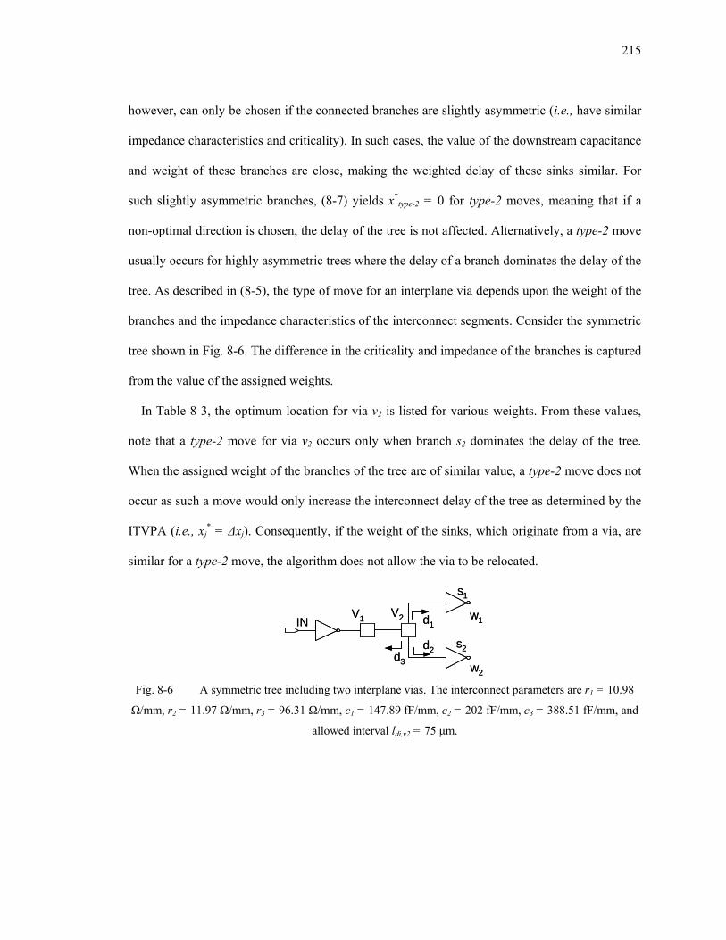
215
however, can only be chosen if the connected branches are slightly asymmetric (i.e., have similar
impedance characteristics and criticality). In such cases, the value of the downstream capacitance
and weight of these branches are close, making the weighted delay of these sinks similar. For
such slightly asymmetric branches, (8-7) yields x*type-2 = 0 for type-2 moves, meaning that if a
non-optimal direction is chosen, the delay of the tree is not affected. Alternatively, a type-2 move
usually occurs for highly asymmetric trees where the delay of a branch dominates the delay of the
tree. As described in (8-5), the type of move for an interplane via depends upon the weight of the
branches and the impedance characteristics of the interconnect segments. Consider the symmetric
tree shown in Fig. 8-6. The difference in the criticality and impedance of the branches is captured
from the value of the assigned weights.
In Table 8-3, the optimum location for via v2 is listed for various weights. From these values,
note that a type-2 move for via v2 occurs only when branch s2 dominates the delay of the tree.
When the assigned weight of the branches of the tree are of similar value, a type-2 move does not
occur as such a move would only increase the interconnect delay of the tree as determined by the
ITVPA (i.e., xj* = ∆xj). Consequently, if the weight of the sinks, which originate from a via, are
similar for a type-2 move, the algorithm does not allow the via to be relocated.
V1 V2
s2
s1
w2
w1IN
d3
d1
d2
V1 V2
s2
s1
w2
w1IN
d3
d1
d2
Fig. 8-6 A symmetric tree including two interplane vias. The interconnect parameters are r1 = 10.98
Ω/mm, r2 = 11.97 Ω/mm, r3 = 96.31 Ω/mm, c1 = 147.89 fF/mm, c2 = 202 fF/mm, c3 = 388.51 fF/mm, and
allowed interval ldi,v2 = 75 µm.

216
TABLE 8-2 OPTIMIZATION RESULTS FOR VARIOUS INTERPLANE INTERCONNECT TREES FOR DIFFERENT
NUMBER OF SINKS AND PHYSICAL PLANES n.
n Number of sinks
Avg. branch length [µm]
Avg. maximum
branch length [µm]
ldi’s [µm]
Delay improvement [%]
Instances xi* = ldi / 2 xi
* = 0
Avg Max Avg Max
3 4 153 186 50 2.72 9.33 3.79 11.25 10000 3 4 307 376 100 4.23 15.17 6.03 17.94 10000 4 4 208 273 50 1.11 3.53 2.49 5.63 5000 4 4 828 1100 200 3.12 10.29 6.42 13.50 5000 4 4 1243 1650 300 4.07 14.15 7.76 19.38 5000 4 8 431 569 100 3.90 13.24 7.71 19.68 10238 5 4 264 362 50 1.25 3.83 2.40 5.89 5000 5 4 1054 1452 200 3.62 11.55 6.56 12.04 5000 5 4 791 1089 300 3.90 11.61 6.95 19.34 5000 5 8 454 660 50 0.90 2.69 2.27 4.98 5000 5 8 521 738 100 1.78 5.55 4.33 8.40 5000 5 8 779 1111 150 2.38 7.44 5.67 11.90 5000 5 8 1038 1481 200 2.91 8.71 6.74 12.58 5000 6 8 306 455 50 1.11 3.17 2.36 4.89 5000 6 8 615 913 100 2.00 5.44 4.09 9.85 5000 6 8 922 1373 150 2.72 7.01 5.43 11.72 5000 6 8 921 1371 200 3.32 10.02 6.61 14.21 5000 6 16 555 845 50 0.86 2.74 2.52 4.95 4970 6 16 637 934 100 1.68 4.82 4.84 9.26 5059 6 16 953 1404 150 2.28 6.10 6.32 12.96 5021
TABLE 8-3 OPTIMAL VIA LOCATION, DIRECTION OF MOVE, AND TYPE OF MOVE FOR VIA v2 SHOWN IN
FIG. 8-6, AS DETERMINED FROM ITVPA FOR VARIOUS VALUES OF w1 AND w2.
w1 w2 x*v2 [µm] Move Direction, di w1 w2 x*
v2 [µm] Move Direction, di 0.50 0.05 ∆xv2 type-1 d0 0.45 0.55 ∆xv2 type-2 d10.55 0.45 ∆xv2 type-1 d0 0.40 0.60 ∆xv2 type-1 d0
0.60 0.40 ∆xv2 type-2 d1 0.35 0.65 ∆xv2 type-2 d20.65 0.35 ∆xv2 type-2 d1 0.30 0.70 ∆xv2 type-2 d20.70 0.30 ∆xv2 type-2 d1 0.25 0.75 ∆xv2 type-2 d2
0.75 0.25 ∆xv2 type-2 d1 0.20 0.80 ∆xv2 type-2 d20.80 0.20 ∆xv2 type-2 d1 0.15 0.85 ∆xv2 type-2 d20.85 0.15 ∆xv2 type-2 d1 0.10 0.90 ∆xv2 type-2 d2
0.90 0.10 ∆xv2 type-2 d1 0.05 0.95 ∆xv2 type-2 d20.95 0.05 ∆xv2 type-2 d1 0.03 0.97 68.70 type-2 d2
The improvement in delay of the interconnect trees is listed in columns 6 through 9 of Table
8-2. The results are compared to the case where the vias are initially placed at the center of the
allowed interval (i.e., xi = ldi / 2) and to the case where the vias are placed at the lower edge of the
allowed interval (i.e., xi = 0). The improvement in delay depends upon the length of the allowed
interval. This dependence, however, is weak as compared to two-terminal nets. In addition, the
improvement in delay is lower than point-to-point nets for the same allowed length intervals. This
reduction in delay improvement occurs for two reasons.

217
For those vias with degree greater than two, which constitute the majority of interplane vias in
interconnect trees, after the type of move for each via is determined, the actual interval length that
these vias are allowed to move is ldi / 2 and not ldi (see Fig. 8-2). Furthermore, in ITVPA, any
modifications to the routing tree are strictly confined within the allowed interval such that least
affects the routing tree. This constraint requires an additional interconnect segment for type-2
moves. If this constraint is relaxed, an additional interconnect segment is not necessary and the
length of the interconnect segments can be further reduced, resulting in a considerably greater
improvement in speed. Maintaining fixed paths limits the efficiency of the algorithms; however,
these algorithms are applicable to placement and routing tool for 3-D ICs as long as these tools
provide an allowed interval for via placement. In addition, interconnect routing can consider other
important design objectives such as thermal effects or routing congestion. These algorithms for
placing vias in multi-terminal nets can be applied as a subsequent post processing step without
significantly affecting the initial layout produced by existing tools.
In Table 8-4, placement results for single critical branch interconnect trees are reported. The
improvement in the delay of these trees is listed in columns 6 through 9 of Table 8-4, as
compared to the situation where the vias are initially placed at the center of the allowed interval
(i.e., xi = ldi / 2) and where the vias are placed at the lower edge of the allowed interval (i.e., xi =
0). This improvement is lower than for those interconnect trees listed in Table 8-4 as only type-1
moves can occur for the off path vias. Indeed, any type-2 move for the off path via only increases
the off path capacitance and, in turn, the delay of the critical leaf. A smaller number of vias can,
therefore, be relocated to reduce the delay of the single critical sink trees. Alternatively, for off
path vias, placing the via at the center of the allowed intervals usually produces an optimum
placement, resulting in a smaller overall improvement in the delay of this type of tree, as is

218
demonstrated by the test structures. This situation occurs because type-2 moves for the off path
vias are not allowed since a type-2 move results in an increase in the off path capacitance.
Typically, the larger the allowed interval, the greater the improvement in delay. Consequently,
efficient placement tools for 3-D circuits that generate sufficiently large allowed intervals are
desired. These intervals can be available space reserved for interplane interconnect routing. For
interconnect trees, the improvement in delay is smaller than for two-terminal nets. This decreased
improvement in delay is due to the constraint of placing the vias within the allowed intervals in
order to minimally affect the local routing congestion. If the placement of the vias is permitted
within an entire region (e.g., the bounding box of the net), a greater decrease in delay can occur.
Assigning such a region for placing vias, however, increases the congestion within a 3-D circuit
as the same number of vias compete for sparser routing resources.
Despite the considerably lower computational time of these algorithms, further speed
improvements can be achieved if more than one net are simultaneously processed. Although these
algorithms support multiple net optimization without significant modification, a single net at a
time approach likely yields improved results as the most critical nets are routed first. Net ordering
algorithms [20] can be used to prioritize the routing of these interconnects, permitting the delay of
these nets to be considerably reduced. Additionally, since the number of interplane interconnects
is small as compared to the number of intraplane interconnects [122], processing these
interconnects one net at a time will not significantly increase the total computational time.
Thermal issues are important in 3-D ICs as discussed in Chapter 6, where additional dummy
vias are utilized to control the average and peak temperature of the upper planes within a 3-D
system. Additionally, thermally aware cell placement improves the heat distribution and removal
characteristics. These two techniques are decoupled from the via placement problem which is

219
considered a later step in the design process. Consequently, thermal issues are not strongly
connected with the via placement approach.
TABLE 8-4 OPTIMIZATION RESULTS FOR VARIOUS SINGLE CRITICAL SINK INTERCONNECT TREES FOR
DIFFERENT NUMBER OF SINKS AND PHYSICAL PLANES n.
n Number of sinks
Avg. branch length [µm]
Avg. maximum branch length
[µm] ∆xi’s [µm]
Delay improvement [%] Instances xi
* = ∆xi / 2 xi* = 0
Avg Max Avg Max 4 4 341 453 50 2.72 8.95 3.70 14.63 5000 4 4 1021 1363 150 1.61 5.52 2.18 11.01 5000 4 4 1368 1821 200 1.36 5.49 1.92 8.59 5000 5 4 433 595 50 3.09 9.37 4.55 19.44 5000 5 4 1299 1790 150 1.80 5.55 2.85 13.42 5000 5 4 1734 2391 200 1.51 5.66 2.44 11.35 5000 5 8 427 612 50 2.53 8.10 4.09 16.20 5000 5 8 853 1227 100 1.94 7.22 2.98 12.63 5000 5 8 1282 1845 150 1.57 6.55 2.46 14.04 5000 5 8 1711 2461 200 1.33 4.81 2.25 10.44 5000 6 8 505 753 50 2.88 8.90 4.39 17.8 5000 6 8 1009 1512 100 2.14 6.10 3.45 15.20 5000 6 8 1511 2265 150 1.71 5.46 2.83 12.16 5000 6 16 523 779 50 2.52 8.29 4.54 13.25 4963 6 16 1045 1564 100 1.91 6.69 3.10 10.53 4977 6 16 1563 2351 150 1.55 5.36 2.96 12.37 4976
In the techniques discussed in Chapter 6, the thermal vias are placed in the available space
among the blocks with either uniform or non-uniform densities. Alternatively, some of the
thermal vias within this available space can be replaced with signal vias connecting circuits on
different planes. Placing the signal vias prior to placing the thermal vias within these regions
results in large allowed intervals, thereby improving the effectiveness of this via placement
technique. In this case, where the via placement can significantly enhance the thermal profile of a
physical plane, the allowed interval for some vias can be decreased or removed. Such a practice,
however, trades off performance for thermal management.
8.5. Summary
Algorithms for the timing-driven placement of interplane interconnect trees is presented in this
chapter. The primary characteristics of these algorithms are:

220
• Several types of moves exist for interplane vias, requiring the insertion of either intraplane or
interplane vias. Moves that require additional interplane vias are excluded to maintain a low
interplane via density.
• The weighted summation of the delay at the sinks of a tree is the objective function that is
minimized.
• A two step heuristic is presented. The direction of the move for each via is initially
determined followed by the second step, where the via is placed to minimize the delay.
• Another heuristic for placing interplane vias within trees to minimize the delay of the critical
path is provided.
• Both of these heuristics exhibit linear complexity with the number of interplane vias.
• The improvement in delay depends upon the size of the allowed intervals for placing each
via.

221
Chapter 9. 3-D Topologies for Networks-on-
Chip
Networks-on-chip (NoC) is a developing design paradigm to enhance interconnections with
complex integrated systems. These networks have an interconnect structure which provide
internet-like communication among various elements of the network; however, on-chip networks
differ from traditional interconnection networks in that communication among the network
elements is implemented through the on-chip routing layers rather than the metal tracks of the
package or printed circuit board (PCB).
NoC offer high flexibility and regularity, supporting simpler interconnect models and greater
fault tolerance. The canonical interconnect backbone of the network combined with appropriate
communication protocols enhance the flexibility of these systems [30]. NoC provide
communication among a variety of functional intellectual property (IP) blocks or processing
elements (PE), such as processor and DSP cores, memory blocks, FPGA blocks, and dedicated
hardware, serving a plethora of applications that include image processing, personal devices, and
mobile handsets, [252]-[254] (the terms IP block and PEs are interchangeably used in this chapter
to describe functional structures connected by a NoC). The intra-PE delay, however, cannot be
reduced by the network. Furthermore, the length of the communication channel is primarily
determined by the area of the PE, which is typically unaffected by the network structure. By
merging vertical integration with NoC, many of the individual limitations of 3-D ICs and NoC are
circumvented, yielding a robust design paradigm with unprecented capabilities.
Research in 3-D NoC is only now emerging [220], [255]-[257]. Addo-Quaye [220] recently
presented an algorithm for the thermal-aware mapping and placement of 3-D NoC including
222
regular mesh topologies. Li et al. [257] proposed a similar 3-D NoC topology employing a buss
structure for communicating among PEs located on different physical planes. Targeting multi-
processor systems, the proposed scheme in [257] considerably reduces cache latencies by
utilizing the third dimension. Multi-dimensional interconnection networks have been studied
under various constraints, such as constant bisection-width and pin-out constraints [258]. NoC
differ from generic interconnection networks, however, in that NoC are not limited by the channel
width or pin-out. Alternatively, physical constraints specific to 3-D NoC, such as the number of
nodes that can be implemented in the third dimension and the asymmetry in the length of the
channels of the network, have to be considered.
In this chapter, various possible topologies for 3-D NoC are presented. Additionally, analytic
models for the zero-load latency and power consumption with delay constraints of these networks
that capture the effects of the topology on the performance of 3-D NoC are described. Optimum
topologies are shown to exist that minimize the zero-load latency and power consumption of a
network. These optimum topologies depend upon a number of parameters characterizing both the
router and the communication channel, such as the number of ports of the network, the length of
the communication channel, and the impedance characteristics of the interconnect. Various
tradeoffs among these parameters that determine the minimum latency and power consumption
topology of a network are investigated for different network sizes.
Several interesting topologies, which are the topic of this chapter, emerge by incorporating the
third dimension in NoC. In the following section, various topological choices for 3-D NoC are
reviewed. In Section 9.2, an analytic model of the zero-load latency of traditional interconnection
networks is adapted for each of the proposed 3-D NoC topologies, while the power consumption
model of these network topologies is described in Section 9.3. In Section 9.4, the 3-D NoC
topologies are compared in terms of the zero-load network latency and power consumption with

223
delay constraints, and guidelines for the optimum design of speed driven or power driven NoC
structures are provided. Finally, some conclusions are offered in Section 9.5.
9.1. 3-D NoC Topologies
Various topologies for 3-D networks are presented and related terminology is introduced in this
section. Mesh structures have been a popular network topology for conventional 2-D NoC [259],
[260]. A fundamental element of a mesh network is illustrated in Fig. 9-1a, where each
processing element (PE) is connected to the network through a router. A PE can be integrated
either on a single physical plane (2-D IC) or on several physical planes (3-D IC). Each router in a
2-D NoC is connected to a neighboring router in one of four directions. Consequently, each router
has five ports. Alternatively, in a 3-D NoC, the router typically connects to two additional
neighboring routers located on the adjacent physical planes. The architecture of the router is
considered here to be a canonical router with input and output buffering [261]. The combination
of a PE and router is called a network node. For a 2-D mesh network, the total number of nodes N
is N = n1 × n2, where ni is the number of nodes included in the ith physical dimension.
Integration in the third dimension introduces a variety of topological choices for NoCs. For a 3-
D NoC as shown in Fig. 9-1b, the total number of nodes is N = n1 × n2 × n3, where n3 is the
number of nodes in the third dimension. In this topology, each PE is on a single yet possibly
different physical plane (2-D IC – 3-D NoC). Alternatively, a PE can be implemented on only one
of the n3 physical planes of the system and, therefore, the 3-D system contains n1 × n2 PEs on
each one of the n3 physical planes such that the total number of nodes is N. This topology is
discussed in [220] and [257]. A 3-D NoC topology is illustrated in Fig. 9-1c, where the
interconnect network is contained within one physical plane (i.e., n3 = 1), while each PE is
integrated on multiple planes, notated as np (3-D IC – 2-D NoC). Finally, a hybrid 3-D NoC based

224
on the two previous topologies is depicted in Fig. 9-1d. In this NoC topology, both the
interconnect network and the PEs can span more than one physical plane of the stack (3-D IC – 3-
D NoC). In the following section, latency expressions for each of the NoC topologies are
described, assuming a zero-load model.
9.2. Zero-Load Latency for 3-D NoC
In this section, analytic models of the zero-load latency of each of the 3-D NoC topologies are
described. The zero-load network latency is widely used as a performance metric in traditional
interconnection networks [262]. The zero-load latency of a network is the latency where only one
packet traverses the network. Although such a model does not consider contention among
packets, the zero-load latency model can be used to describe the effect of a topology on the
performance of a network. The zero-load latency of an NoC with wormhole switching is [262]
b
LtthopsT p
crnetwork ++⋅= , (9-1)
where the first term is the routing delay, tc is the propagation delay along the wires of the
communication channel, which is also called a buss here for simplicity, and the third term is the
serialization delay of the packet. hops is the average number of routers that a packet traverses to
reach the destination node, tr is the router delay, Lp is the length of the packet in bits, and b is the
bandwidth of the communication channel defined as b ≡ wcfc, where wc is the width of the
channel in bits and fc is the inverse of the propagation delay of a bit along the longest
communication channel.
Since the number of planes that can be stacked in a 3-D NoC is constrained by the target
technology, n3 is also constrained. Furthermore, n1, n2, and n3 are not necessarily equal. The
average number of hops in a 3-D NoC is

225
)1(3
)()(
321
21213321321
−−+−++
=nnn
nnnnnnnnnnnhops , (9-2)
assuming dimension-order routing such that the minimum distance paths are used for the routing
of packets between any source-destination node pair. The number of hops in (9-2) can be divided
into two components, the average number of hops within the two dimensions n1 and n2, and the
average number of hops within the third dimension n3,
)1(3
)1)((
321
212132 −
−+=− nnn
nnnnnhops D , (9-3)
)1(3
)1(
321
2123
3 −−
=− nnnnnn
hops D . (9-4)
Fig. 9-1 Various NoC topologies (not to scale), (a) 2-D IC – 2-D NoC, (b) 2-D IC – 3-D NoC, (c) 3-D
IC – 2-D NoC, and (d) 3-D IC – 3-D NoC.
NoC
IC 2-D 3-D
2-D
(a) (b)
3-D
(c) (d)

226
The delay of the router tr is the sum of the delay of the arbitration logic ta and the delay of the
switch ts, which in this chapter is considered to be implemented with a classic crossbar switch
[262],
sar ttt += . (9-5)
The delay of the arbiter can be described from [263],
( )τ9)12/1(14log)4/1(21 2 ++= pta , (9-6)
where p is the number of ports of the router and τ is the delay of a minimum sized inverter for the
target technology. Note that (9-6) exhibits a logarithmic dependence on the number of router
ports. The length of the crossbar switch also depends upon the number of router ports and the
width of the buss,
pwswl ctts )(2 += , (9-7)
where wt and st are the width and spacing or, alternatively, the pitch of the interconnect,
respectively, and wc is the width of the communication channel in bits. Consequently, the worst
case delay of the crossbar switch is determined by the longest path within the switch, which is
equal to (9-7).
The delay of the communication channel tc is
DhDvc hopsthopstt −− += 23 , (9-8)
where tv and th are the delay of the vertical and horizontal channels, respectively (see Fig. 9-1b).
Note that if n3 = 1, (9-8) describes the propagation delay of a 2-D NoC. Substituting (9-8) and (9-
5) into (9-1), the overall zero-load network latency for a 3-D NoC is
hc
pvDhDsanetwork t
wL
thopsthopstthopsT ++++= −− 32)( . (9-9)

227
To characterize ts, th, and tv, the models described in [264] are adopted, where repeaters
implemented as simple inverters are inserted along the interconnect. According to these models,
the propagation delay and rise time of a single interconnect stage for a step input, respectively,
are
⎟⎟⎠
⎞⎜⎜⎝
⎛+++=
i
igii
ii
iidd
i
iiidi k
hClrkh
lcRCR
klcr
t 00002
2
377.0 , (9-10)
⎟⎟⎠
⎞⎜⎜⎝
⎛+++=
i
igii
ii
iirr
i
iiiri k
hClrkh
lcRCR
klcr
t 00002
2
75.21.1 , (9-11)
where ri (ci) is the per unit length resistance (capacitance) of the interconnect and li is the total
length of the interconnect. The index i is used to notate the various interconnect delays included
in the network (i.e., i ∈ s,v,h). hi and ki denote the number and size of the repeaters,
respectively, and Cg0 and C0 represent the gate and total input capacitance of a minimum sized
device, respectively. C0 is the summation of the gate and drain capacitance of the device. Rr0 and
Rd0 describe the equivalent output resistance of a minimum sized device for the propagation delay
and transition time of a minimum sized inverter, respectively, where the output resistance is
approximated as
0
)(0)(dn
dddrdr I
VKR = . (9-12)
K denotes a fitting coefficient and Idn0 is the drain current of an NMOS device at both Vds and Vgs
equal to Vdd. The value of these device parameters are listed in Table 9-1. A 45 nm technology
node is assumed and SPICE simulations of the predictive technology library are used to
determine the individual parameters [247], [248].
To include the effect of the input slew rate on the total delay of an interconnect stage, (9-10)
and (9-11) are further refined by including an additional coefficient γ as in [265],

228
n
dd
tn
r aV
V
−
−−=
1
1
21γ . (9-13)
By substituting the subscript n with p, the corresponding value for a falling transition is obtained.
The average value γ of γr and γf is used to describe the effect of the transition time on the
interconnect delay. The overall interconnect delay can therefore be described as
⎟⎟⎠
⎞⎜⎜⎝
⎛ +++=+= hCRh
lcRkCRa
cr
attkt giii
i
iridii 0
00021)γ( , (9-14)
where R0, a1, and a2 are described in [266] and the index i denotes the various interconnect
structures such as the crossbar switch (i ≡ s), the horizontal buss (i ≡ h), and the vertical buss (i ≡
v).
For minimum delay, the size h and number k of repeaters are determined by setting the partial
derivative of ti with respect to hi and ki, respectively, equal to zero and solving for hi and ki,
002
21*
CRalcra
k iiii = , (9-15)
0
0*
gi
iii Cr
lcRh = . (9-16)
The expression in (9-14) only considers RC interconnects. An RC model is sufficiently accurate
to characterize the delay of a crossbar switch since the length of the longest wire within the
crossbar switch and the signal frequencies are such that inductive behavior is not prominent. For
the buss lines, however, inductive behavior can appear. For this case, suitable expressions for the
delay and repeater insertion characteristics can be adopted from [267]. For the target operating
frequencies (1 to 2 GHz) and buss length (< 2 mm) considered in this chapter, an RC interconnect
model provides sufficient accuracy [268]. Additionally, for the vertical buss, kv = 1 and hv = 1,

229
meaning that no repeaters are inserted and minimum sized drivers are utilized. Repeaters are not
necessary due to the short length of the vertical buss. Driving a buss with minimum sized
inverters can affect the resulting minimum latency and power dissipation topology, as discussed
in the following sections. Note that the proposed latency expression includes the effect of the
input slew rate. Additionally, since a repeater insertion methodology for minimum latency is
applied, any further reduction in latency is due to the network topology.
TABLE 9-1 INTERCONNECT AND DESIGN PARAMETERS, 45 nm TECHNOLOGY.
Parameter Value NMOS PMOS
Wmin 100 nm 250 nm Idsat/W 1115 µΑ/µm 349 µΑ/µm Vdsat 478 mV -731 mV Vt 257 mV -192 mV a 1.04 1.33
Isub0 48.8 nA Ig0 0.6 nA Vdd 1.1 Volts
Temp. 110 oC Kd 0.98 Kr 0.63 Cg0 512 fF Cd0 487 fF τ 17 ps
The length of the vertical communication channel for the 3-D NoC shown in Fig. 9-1 is
⎪⎩
⎪⎨
⎧
−−
−−
=
NoC,2DIC3DandNoC2DIC2Dfor,0
NoC3DIC3Dfor,NoC3DIC2Dfor,
vp
v
v LnL
l (9-17a)(9-17b)
(9-17c)
where Lv is the length of a silicon-through (interplane) via connecting two routers on adjacent
physical planes. np is the number of physical planes used to integrate each PE. The length of the
horizontal communication channel is assumed to be
⎪⎧ −− NoC3DIC2DandNoC2DIC2Dfor,PEA (9-18a)

230
(9-18b)
where APE is the area of the processing element. The area of all of the PEs and, consequently, the
length of each horizontal channel are assumed to be equal. For those cases where the PE is
implemented in multiple physical planes, a coefficient is included to consider the effect of the
interplane vias on the reduction in the ideal wirelength due to utilization of the third dimension.
The value of this coefficient (= 1.12) is based on the layout of a crossbar switch designed with the
fully depleted silicon-on-insulator (FDSOI) 3-D technology from MIT Lincoln Laboratory
(MITLL) [139]. The same coefficient is also assumed for the design of the PEs on more than one
physical plane. In the following section, expressions for the power consumption of a network
with delay constraints are presented.
9.3. Power Consumption in 3-D NoC
Power dissipation is a critical issue in three-dimensional circuits. Although the total power
consumption of 3-D systems is expected to be lower than that of mainstream 2-D circuits (since
the global interconnects are shorter [140]), the increased power density is a challenging issue for
this novel design paradigm. Therefore, those 3-D NoC topologies that offer low power
characteristics should be of significant interest.
The different power consumption components for interconnects with repeaters are briefly
discussed in this section. Due to specified performance characteristics, a low power design
methodology with delay constraints for the interconnect in an NoC is adopted from [266]. An
expression for the total power consumption per bit of a packet transferred between a source
destination node pair is used as the basis for characterizing the power consumption of an NoC for
the 3-D topologies.
The power consumption components of an interconnect line with repeaters are:

231
(a) Dynamic power consumption is the dissipated power due to the charge and discharge of the
interconnect and input gate capacitance during a signal transition, and can be described by
2)( ddoiiiisdi VCkhlcfaP += , (9-19)
where f is the clock frequency and as is the switching factor [269]. A value of 0.15 is assumed
here; however, for NoC, the switching factor can vary considerably. This variation, however,
does not affect the power comparison for the various topologies as the same switching factor is
incorporated in each term for the total power consumed per bit of the network (the absolute value
of the power consumption, however, changes).
(b) Short-circuit power is due to the DC current path that exists in a CMOS circuit during a signal
transition when the input signal voltage changes between Vtn and Vdd + Vtp. The power
consumption due to this current is described as short-circuit power and is modeled in [270] by
irideffidsat
iiddridssi htHIGCV
hkVtfIaP
0
2220
24
+= , (9-20)
where Id0 is the average drain current of the NMOS and PMOS devices operating in the saturation
region and the value of the coefficients G and H are described in [271]. Due to resistive shielding
of the interconnect capacitance, an effective capacitance is used in (9-20) rather than the total
interconnect capacitance. This effective capacitance is determined from the methodology
described in [272] and [273].
(c) Leakage power is comprised of two power components, the subthreshold and gate leakage
currents. The subthreshold power consumption is due to current flowing during the cut-off region
(below threshold), causing Isub current to flow. The gate leakage component is due to current
flowing through the gate oxide, denoted as Ig. The total leakage power can be described as
)( 00 gsubddiili IIVkhP += , (9-21)

232
where the average subthreshold Isub0 and gate Ig0 leakage current of the NMOS and PMOS
transistors is used in (9-21).
The total power consumption with delay constraint T0 for a single line of a crossbar switch
Pstotal, horizontal buss Phtotal, and vertical buss Pvtotal is, respectively,
lisidiastotal PPPtTP ++=− )( 0 , (9-22)
lisidihtotal PPPTP ++=)( 0 , (9-23)
lisidivtotal PPPTP ++=)( 0 . (9-24)
The power consumption of the arbitration logic is not included in (9-22), since most of the
power is consumed by the crossbar switch and the buss interconnect, as discussed in [274]. Note
that for a crossbar switch, the additional delay ta of the arbitration logic poses a stricter delay
constraint on the power consumption of the switch as shown in (9-22). The minimum power
consumption with delay constraints is determined by the methodology described in [266], for
which the optimum size h*powi and number k*
powi of the repeaters for a single interconnect line is
determined. Consequently, the minimum power consumption per bit between a source destination
node pair in a NoC with a delay constraint is
vtotalDhtotalDstotalbit PhopsPhopshopsPP −− ++= 32 . (9-25)
The effect of resistive shielding is also considered in determining the effective interconnect
capacitance. Furthermore, since the repeater insertion methodology in [266] minimizes the power
consumed by the repeater system, any additional decrease in power consumption is due only to
the network topology. In the following section, those 3-D NoC topologies that exhibit the
maximum performance and minimum power consumption with delay constraints are presented.
Tradeoffs in determining these topologies are discussed and the impact of the network parameters
on the resulting optimum topologies are demonstrated for various network sizes.

233
9.4. Performance and Power Analysis for 3-D NoC
Several network parameters characterizing the topology of a network can significantly affect the
speed and power of a system. The evaluation of these network parameters is discussed in Section
9.4.1. The improvement in network performance achieved by the 3-D NoC topologies is explored
in Section 9.4.2. The distribution of nodes that produces the maximum performance is also
discussed. The power consumption with delay constraints of a 3-D NoC and the topologies that
yield the minimum power consumption of a 3-D NoC are presented in Section 9.4.3.
9.4.1. Parameters of 3-D Networks-on-Chip
The physical layer of a 3-D NoC consists of different interconnect structures, such as a crossbar
switch, the horizontal buss connecting neighboring nodes on the same physical plane, and the
vertical buss connecting nodes on different, not necessarily adjacent, physical planes. The device
parameters characterizing the receiver, driver, and repeaters are listed in Table 9-1. The
interconnect parameters reported in Table 9-2 are different for each type of interconnect within a
network.
A typical interconnect structure is shown in Fig. 9-2, where three parallel metal lines are
sandwiched between two ground planes. Such an interconnect structure is considered for the
crossbar switch (at the network nodes) where the intermediate metal layers are assumed to be
utilized. The horizontal buss is implemented on the global metal layers and, therefore, only the
lower ground plane is present in this structure for a 2-D NoC. For a 3-D NoC, however, the
substrate (back-to-front plane bonding) or a global metal layer of an upper plane (front-to-front
plane bonding) behaves as a second ground plane. To incorporate this additional ground plane,
the horizontal bus capacitance is changed by the coefficient a3-D. A second ground plane
decreases the coupling capacitance to an adjacent line, while the line-to-ground capacitance
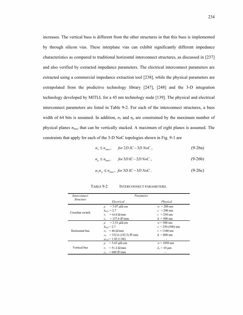
234
increases. The vertical buss is different from the other structures in that this buss is implemented
by through silicon vias. These interplane vias can exhibit significantly different impedance
characteristics as compared to traditional horizontal interconnect structures, as discussed in [237]
and also verified by extracted impedance parameters. The electrical interconnect parameters are
extracted using a commercial impedance extraction tool [238], while the physical parameters are
extrapolated from the predictive technology library [247], [248] and the 3-D integration
technology developed by MITLL for a 45 nm technology node [139]. The physical and electrical
interconnect parameters are listed in Table 9-2. For each of the interconnect structures, a buss
width of 64 bits is assumed. In addition, n3 and np are constrained by the maximum number of
physical planes nmax that can be vertically stacked. A maximum of eight planes is assumed. The
constraints that apply for each of the 3-D NoC topologies shown in Fig. 9-1 are
NoCDICDfornn 32,max3 −≤ , (9-26a)
NoCDICDfornnp 23,max −≤ , (9-26b)
NoCDICDfornnn p 33,max3 −≤ . (9-26c)
TABLE 9-2 INTERCONNECT PARAMETERS.
Interconnect Structure
Parameter
Electrical Physical
Crossbar switch
ρ = 3.07 µΩ-cm w = 200 nm kILD = 2.7 s = 200 nm rs = 614 Ω/mm t = 250 nm cs = 157.6 fF/mm h = 500 nm
Horizontal bus
ρ = 2.53 µΩ-cm w = 500 nm kILD = 2.7 s = 250 (500) nm rh = 46 Ω/mm t = 1100 nm ch = 332.6 (192.5) fF/mm h = 800 nm a3-D = 1.02 (1.06) -
Vertical bus ρ = 5.65 µΩ-cm w = 1050 nm rv = 51.2 Ω/mm Lv = 10 µm cv = 600 fF/mm -

235
Fig. 9-2 Typical interconnect structure for intermediate metal layers.
A small set of parameters is used as variables to explore the performance and power
consumption of the 3-D NoC topologies. This set includes the network size or, equivalently, the
number of nodes within the network N, the area of each processing element APE, which is directly
related to the buss length as described in (9-18), and the maximum allowed interconnect delay
when evaluating the minimum power consumption with delay constraints. The range of values for
these variables is listed in Table 9-3. Depending upon the network size, NoC are roughly divided
as small (N = 16 to 64 nodes), medium (N = 128 to 256 nodes), and large (N = 512 to 2048
nodes) networks. For multi-processor SoC networks, sizes of up to N = 256 is expected to be
feasible in the near future [257], [275], whereas for NoC with a finer granularity, where the PEs
each corresponds to hardware blocks of approximately 100K gates, network sizes over a few
thousands nodes are predicted at the 45 nm technology node [276]. Note that this classification of
the networks is not strict and is only intended to facilitate the discussion in the following sections.
TABLE 9-3 NETWORK PARAMETERS.
Parameter Values
N 16, 32, 64, 128, 256, 512, 1024, 2048
APE [mm2] 0.5, 0.64, 0.81, 1.00, 1.56, 2.25, 4.00
T0 [ps] 1000, 500
9.4.2. Performance Tradeoffs for 3-D NoC
The performance enhancements that can be achieved in NoC by utilizing the third dimension are
investigated in this subsection. Each of the 3-D topologies decreases the zero-latency of the

236
network by reducing different delay components, as described in (9-9). In addition, the
distribution of network nodes in each physical dimension that yields the minimum zero-load
latency is shown to significantly change with the network and interconnect parameters.
1) 2-D IC – 3-D NoC
Utilizing the third dimension to implement a NoC results directly in a decrease in the average
number of hops for packet switching. The average number of hops on the same plane hops2-D (the
intraplane hops) and the average number of hops in the third dimension hops3-D (the interplane
hops) are also reduced. Interestingly, the distribution of nodes n1, n2, and n3 that yields the
minimum total number of hops is not always the same as the distribution that minimizes the
number of intraplane hops. This situation occurs particularly for small and medium networks,
while for large networks, the distribution of n1, n2, and n3 which minimizes the hops also
minimizes hops2-D.
In a 3-D NoC, the number of router ports increases from five to seven, increasing, in turn, both
the switch and arbiter delay. Furthermore, a short vertical buss generally exhibits a lower delay
than that of a relatively long horizontal buss. In Fig. 9-3, the zero-load latency of the 2-D IC – 3-
D NoC is compared to that of the 2-D IC – 2-D NoC for different network sizes. A decrease in
latency of 15.7% and 20.1% can be observed for N = 128 and N = 256 nodes, respectively, with
APE = 0.81 mm2.

237
4 5 6 7 8 9 10 110
2
4
6
8
10
12
14
16
Late
ncy
[ns]
Number of nodes log2N
2D IC - 2D NoC2D IC - 3D NoC
(a)
4 5 6 7 8 9 10 110
5
10
15
20
25
Late
ncy
[ns]
Number of nodes log2N
2D IC - 2D NoC2D IC - 3D NoC
(b) Fig. 9-3 Zero-load latency for various network sizes. (a) APE = 0.81 mm2 and ch = 332.6 fF/mm, (b)
APE = 4 mm2 and ch = 332.6 fF/mm.
The node distribution that produces the lowest latency varies with network size. For example,
n3max = 8 is not necessarily the optimum for small and medium networks, although by increasing
n3, more hops occur through the short, low latency vertical channel. This result can be explained

238
by considering the reduction in the number of hops that originate from utilizing the third
dimension for packet switching. For small and medium networks, the decrease in the number of
hops is small and cannot compensate the increase in the routing delay due to the increase in the
number of ports of a router in a 3-D NoC. As the horizontal buss length becomes longer,
however, (e.g., approaching 2 mm), n3 > 1, and a slight decrease in the number of hops
significantly decreases the overall delay, despite the increase in the routing delay for a 3-D NoC.
As an example, consider a network with log2N = 4 and APE = 0.81 mm2. The minimum latency
node distribution is n1 = n2 = 4 and n3 = 1 (identical to a 2-D IC – 2-D NoC as shown in Fig.
9-3), while for APE = 4 mm2, n1 = n2 = 2 and n3 = 4.
The optimum node distribution can also be affected by the delay of the vertical channel. The
repeater insertion methodology for minimum delay as described in Section 9.2 can significantly
reduce the delay of the horizontal buss by inserting large sized repeaters (i.e., h > 300). In this
case, the delay of the vertical buss becomes comparable to that of the horizontal buss with
repeaters. Consider a network with N = 128 nodes. Two different node distributions yield the
minimum average number of hops, specifically, n1 = 4, n2 = 4, and n3 = 8 and n1 = 8, n2 = 4, and
n3 = 4. The first of the two distributions also results in the minimum number of intraplane
Dhops −2 , thereby reducing the latency component for the horizontal buss as described by (9-9).
Simulation results, however, indicate that this distribution is not the minimum latency node
distribution, as the delay due to the vertical channel is non-negligible. For this reason, the latter
distribution with n3 = 4 is preferable, since a smaller number of hops3-D occurs, resulting in the
minimum network latency.
2) 3-D IC – 2-D NoC
For this type of three-dimensional network, the PEs are allowed to span multiple physical planes
while the network effectively remains two-dimensional (i.e., n3 = 1). Consequently, the network

239
latency is only reduced by decreasing the length of the horizontal buss, as described in (9-18).
The routing delay component remains constant with such a 3-D topology. Decreasing the
horizontal buss length lowers both the communication channel delay and the serialization delay.
In Fig. 9-4, the decrease in latency that can be achieved by a 3-D IC – 3-D NoC is illustrated. A
latency decrease of 30.2% and 26.4% can be observed for N = 128 and N = 256 nodes,
respectively, with APE = 2.25 mm2. The use of multiple physical planes reduces the latency;
therefore, the optimum value for np = nmax, regardless of the network size and buss length.
In Figs. 9-5a and 9-5b, the improvement in the network latency over a 2-D IC – 2-D NoC for
various network sizes and for different PE areas (i.e., different horizontal buss length) is
illustrated for the 2-D IC – 3-D NoC and 3-D IC – 2-D NoC topologies, respectively. Note that
for the 2-D IC – 3-D NoC topology, the improvement in delay is smaller for PEs with a larger
area or, equivalently, with longer buss lengths independent of the network size. For longer buss
lengths, the buss latency comprises a larger portion of the total network latency. Since for a 2-D
IC – 3-D NoC only the hop count is reduced, the improvement in latency is lower for longer buss
lengths. Alternatively, the improvement in latency is greater for PEs with a larger area
independent of the network size for 3-D IC – 2-D NoC. This situation is due to the significant
reduction in the PE area (or buss length) that is achieved with this topology. Consequently, there
is a tradeoff in the latency of a NoC that depends both on the network size and the area of the
PEs. In Fig. 9-5a, the improvement is not significant for small networks (all of the curves
converge to approximately zero) in 2-D IC – 3-D NoC while this situation does not occur for 3-D
IC – 2-D NoC. This behavior is due to the increase in the delay of the network router as the
number of ports increases from five to seven for 2-D IC – 3-D NoC, which is a considerable
portion of the network latency for small networks. Note that for 3-D IC – 2-D NoC, the network
essentially remains two dimensional and therefore the delay of the router for this topology does

240
not increase. To achieve the minimum delay, a 3-D NoC topology that exploits these tradeoffs is
described in the following subsection.
4 5 6 7 8 9 10 110
2
4
6
8
10
12
14
16
Late
ncy
[ns]
Number of nodes log2N
2D IC - 2D NoC3D IC - 2D NoC
(a)
4 5 6 7 8 9 10 110
2
4
6
8
10
12
14
16
18
Late
ncy
[ns]
Number of nodes log2N
2D IC - 2D NoC3D IC - 2D NoC
(b) Fig. 9-4 Zero-load latency for various network sizes. (a) APE = 0.64 mm2 and ch = 192.5 fF/mm, (b)
APE = 2.25 mm2 and ch = 192.5 fF/mm.

241
(a)
(b)
Fig. 9-5 Improvement in zero–load latency for different network sizes and PE areas (i.e., buss lengths).
(a) 2-D IC – 3-D NoC and (b) 3-D IC – 2-D NoC.

242
3) 3-D IC – 3-D NoC
This topology offers the greatest decrease in latency over the aforementioned three-dimensional
topologies. The 2-D IC – 3-D NoC topology decreases the number of hops while the buss and
serialization delays remain constant. With the 3-D IC – 2-D NoC, the buss and serialization delay
is smaller but the number of hops remains unchanged. With the 3-D IC – 3-D NoC, all of the
latency components can be decreased by assigning a portion of the available physical planes for
implementing the network while the remaining planes of the stack are used for the PE. The
resulting decrease in network latency as compared to a standard 2-D IC – 2-D NoC and the other
two 3-D topologies is illustrated in Fig. 9-6. A decrease in latency of 40% and 36% can be
observed for N = 128 and N = 256 nodes, respectively, with APE = 4 mm2. Note that the 3-D IC –
3-D NoC topology achieves the greatest savings in latency by optimally balancing n3 with np.
(a)

243
Fig. 9-6 Zero-load latency for various network sizes. (a) APE = 1 mm2 and ch = 332.6 fF/mm, (b) APE
= 4 mm2 and ch = 332.6 fF/mm.
For certain network sizes, the performance of the 3-D IC – 2-D NoC is identical to either the 2-
D IC – 3-D NoC or 3-D IC – 2-D NoC. This behavior occurs because for large network sizes, the
delay due to the large number of hops dominates the total delay and, therefore, the latency can be
primarily reduced by decreasing the average number of hops (n3 = nmax). For small networks, the
buss delay is large and the latency savings is typically achieved by reducing the buss length (np =
nmax). For medium networks, though, the optimum topology is obtained by dividing nmax between
n3 and np such that (9-26c) is satisfied. This distribution of n3 and np as a function of the network
size and buss length is illustrated in Fig. 9-7.
Note the shift in the value of n3 and np as the PE area APE or, equivalently, the buss length
increases. For long busses, the delay of the communication channel becomes dominant and
therefore the smaller number of hops for medium sized networks cannot significantly decrease
(b)

244
the total delay. Alternatively, further decreasing the buss length by implementing the PEs in a
greater number of physical planes leads to a larger savings in delay.
Fig. 9-7 n3 and np values for minimum zero-load latency for various network sizes. (a) APE = 1 mm2
and ch = 332.6 fF/mm, (b) APE = 4 mm2 and ch = 332.6 fF/mm.
4 5 6 7 8 9 10 111
2
3
4
5
6
7
8
n 3
Number of nodes log2N
n p
n3np
4 5 6 7 8 9 10 111
2
3
4
5
6
7
8
(a)
4 5 6 7 8 9 10 111
2
3
4
5
6
7
8
n 3
Number of nodes log2N
n pn3np
4 5 6 7 8 9 10 111
2
3
4
5
6
7
8
(b)

245
The suggested optimum topologies for various network sizes (namely, small, medium, and
large networks) also depend upon the interconnect parameters of the network. Consequently, a
change in the optimum topology for different network sizes can occur when different interconnect
parameters are considered. Despite the sensitivity of the topologies on the interconnect
parameters, the tradeoff between the number of hops and the buss length for various 3-D
topologies (see Fig. 9-5 and Fig. 9-7) can be exploited to improve the performance of an NoC. In
the following subsection, the topology that yields the minimum power consumption with delay
constraints is described. The distribution of nodes for that topology is also discussed.
9.4.3. Power Consumption in 3-D NoC
The various power consumption components for the interconnect within an NoC are analyzed in
Section 9.3. The methodology presented in [266] is applied here to minimize the power
consumption of these interconnects while satisfying the specified operating frequency of the
network. Since a power minimization methodology is applied to the buss lines, the power
consumed by the network can only be further reduced by the choice of network topology.
Additionally, the power consumption also depends upon the target operating frequency, as
discussed later in this section.
As with the zero-load latency, each topology affects the power consumption of the network in a
different way. From (9-25), the power consumption can be reduced by either decreasing the
number of hops for the packet or by decreasing the buss length. Note that by reducing the buss
length, the interconnect capacitance is not only reduced but also the number and size of the
repeaters required to drive the lines are decreased, resulting in a greater savings in power. The
effect of each of the 3-D topologies on the power consumption of an NoC is investigated in this
section.

246
1) 2-D IC – 3-D NoC
Similar to the network latency, the power consumption is decreased in this topology by reducing
the number of hops for packet switching. Again, the increase in the number of ports is significant;
however, the impact from this increase is not as important as that on the latency of the network. A
three-dimensional network, therefore, can reduce power even in small networks. The power
savings achieved with this topology is depicted in Fig. 9-8 for various network sizes, where the
savings is greater in larger networks. This situation occurs because the reduction in the average
number of hops for a three-dimensional network increases for larger network sizes. A power
savings of 26.1% and 37.9% is achieved for N = 128 and N = 512, respectively, with APE = 1
mm2.
4 5 6 7 8 9 10 110
1
2
3
4
5
6
7
Pow
er p
er b
it [m
W]
Number of nodes log2N
2D IC - 2D NoC2D IC - 3D NoC
(a)

247
Fig. 9-8 Power consumption with delay constraints for various network sizes. (a) APE = 1 mm2, ch =
332.6 fF/mm, and T0 = 500 ps, (b) APE = 4 mm2, ch = 332.6 fF/mm, and T0 = 500 ps.
2) 3-D IC – 2-D NoC
With this topology, the number of hops in the network is the same as for a two-dimensional
network. The horizontal buss length, however, is shorter by implementing the PEs in more than
one physical plane. The greater the number of physical planes that can be integrated in a 3-D
system, the larger the power savings, meaning that the optimum value for np with this topology is
always nmax regardless of the network size and operating frequency. The achieved savings is
practically limited by the number of physical planes that can be integrated in a 3-D technology.
The power savings for various network sizes are shown in Fig. 9-9. Note that for this type of
NoC, the maximum performance topology is identical to the minimum power consumption
topology, as the key element of both objectives originates solely from the shorter buss length. The
4 5 6 7 8 9 10 110
2
4
6
8
10
12
Pow
er p
er b
it [m
W]
Number of nodes log2N
2D IC - 2D NoC2D IC - 3D NoC
(b)

248
savings in power is approximately 35% when APE = 0.64 mm2 for every network size as the per
cent reduction in the buss length is the same for each network size.
Fig. 9-9 Power consumption with delay constraints for various network sizes. (a) APE = 0.64 mm2, ch
= 192.5 fF/mm, and T0 = 1000 ps, (b) APE = 2.25 mm2, ch = 192.5 fF/mm, and T0 = 1000 ps.
4 5 6 7 8 9 10 110
0.2
0.4
0.6
0.8
1
1.2
1.4
1.6
1.8
2
Pow
er p
er b
it [m
W]
Number of nodes log2N
2D IC - 2D NoC3D IC - 2D NoC
(a)
4 5 6 7 8 9 10 110
0.5
1
1.5
2
2.5
3
3.5
Pow
er p
er b
it [m
W]
Number of nodes log2N
2D IC - 2D NoC3D IC - 2D NoC
(b)

249
3) 3-D IC – 3-D NoC
Allowing the available physical planes to be utilized either for the third dimension of the network
or for the PEs, the 3-D IC - 3-D NoC scheme achieves the greatest savings in power in addition to
the minimum delay, as discussed in the previous subsection. The distribution of nodes along the
physical dimensions, however, that produces either the minimum latency or the minimum power
consumption for every network size is not necessarily the same. This non-equivalence due to the
different degree of importance of the average number of hops and the buss length in determining
the latency and power consumption of a network. In Fig. 9-10, the power consumption of the 3-D
IC – 3-D NoC topology is compared to the three-dimensional topologies previously discussed. A
power savings of 38.4% is achieved for N = 128 with APE = 1 mm2. For certain network sizes, the
power consumption of the 3-D IC – 3-D NoC topology is the same as that of the 2-D IC – 3-D
NoC and 3-D IC – 2-D NoC topologies. For the 2-D IC – 3-D NoC, the power consumption is
primarily decreased by reducing the number of hops for packet switching, while for the 3-D IC –
2-D NoC, the NoC power dissipation is decreased by shortening the buss length. The former
approach typically benefits small networks, while the latter approach yields lower power
consumption for large networks. For medium sized networks and depending upon the network
and interconnect parameters, non-extreme values for the n3 and np parameters (e.g., 1 < n3 < nmax
and 1 < np < nmax) are required to produce the minimum power consumption topology.
Note that this work emphasizes the latency and power consumption of a network, neglecting
the performance requirements of the individual PEs. If the performance of the individual PEs is
important, only one 3-D topology may be available; however, even with this constraint, a
significant savings in latency and power can be achieved since in almost every case the network
latency and power consumption can be decreased as compared to a 2-D IC – 2-D NoC topology.

250
Furthermore, as previously mentioned, if the available topology is the 2-D IC – 3-D NoC, setting
n3 equal to nmax is not necessarily the optimum choice.
The proposed zero-load network latency and power consumption expressions capture the effect
of the topology; yet these models do not incorporate the effects of the routing scheme and traffic
load. Alternatively, these models can be treated as lower bounds for both the latency and the
power consumption of the network. Since minimum distance paths and no contention are
implicitly assumed in these expressions, non-minimal path routing schemes and heavy traffic
loads will result in increasing both the latency and power consumption of the network. Finally,
the latency and power consumption of the different interconnect structures of the network, which
are shown to be significant, are accurately described by the delay and power expressions and do
not change under any routing conditions and/or traffic load.
(a)

251
Fig. 9-10 Power consumption with delay constraints for various network sizes. (a) APE = 1 mm2, ch =
332.6 fF/mm, and T0 = 500 ps, and (b) APE = 4 mm2, ch = 332.6 fF/mm, and T0 = 500 ps.
9.5. Summary
3-D NoC are a natural evolution for 2-D NoC, exhibiting superior performance. Several novel 3-
D NoC topologies are presented in this chapter and the latency and power consumption of these
topologies are investigated. The primary points of this discussion can be summarized as follows:
• Vertical integration can improve both the latency and power consumption of traditional 2-D
NoC. The minimum latency and power consumption can be achieved by reducing both the
number of hops per packet and the length of the communications channels.
• Expressions for the zero-load network latency and the power consumption components are
described for 3-D NoC.
(b)

252
• NoC that are implemented by a 3-D mesh reduce the number of hops required to propagate a
data packet between two nodes of a network (2-D IC – 3-D NoC).
• A 2-D IC – 3-D NoC decreases the latency and power consumption of a NoC by reducing the
number of hops.
• A 3-D IC – 2-D NoC decreases the latency and power consumption of a NoC by reducing the
buss length or, equivalently, the distance between adjacent network nodes.
• Large networks are primarily benefited by the 2-D IC – 3-D NoC topology, while small
networks are benefited by the 3-D IC – 2-D NoC topology.
• The distribution of nodes that corresponds to either the minimum latency or power
consumption of a network depends upon the interconnect parameters and the network size
and are not necessarily the same.
• A tradeoff exists between the number of planes utilized to implement a network and those
planes to implement the PEs. Consequently and not surprisingly, the 3-D IC – 3-D NoC
topology achieves the greatest improvement in latency and power consumption by most
effectively exploiting the third dimension.

253
Chapter 10. Case Study: Clock Distribution
Networks for 3-D ICs
In the previous chapters, the advantages that result from introducing the third dimension to
integrated circuit applications are discussed. Significant improvement in interconnect
performance and power consumption is predicted for these circuits, constituting an important
opportunity for high performance digital circuits. An omnipresent and challenging issue for
synchronous digital circuits is the reliable distribution of the clock signal to the many hundreds of
thousands of sequential elements distributed throughout a synchronous circuit [277]. The
complexity is further increased in 3-D ICs as sequential elements belonging to the same clock
domain (i.e., synchronized by the same clock signal) can be located on different planes. Another
important issue in the design of the clock distribution network is low power consumption, as the
clock network dissipates a significant portion of the total power consumed by a synchronous
circuit [278], [279]. This demand is stricter for 3-D ICs due to the increased power density and
related thermal limitations, as discussed in Chapter 6.
In 2-D circuits, symmetric interconnect structures, such as H- and X-trees, are widely utilized
to distribute the clock signal across a circuit [280]. The symmetry of these structures permits the
clock signal to simultaneously arrive at the leaves of the tree, resulting in synchronous data
processing. Maintaining this symmetry within a 3-D circuit, however, is a difficult task. In
addition, 3-D ICs include two different types of interconnects, namely intraplane and interplane
interconnects, that can exhibit different impedance characteristics [281]. Furthermore, interplane
interconnects have fixed dimensions determined by the target 3-D technology, further
constraining the design space.

254
In this chapter, a variety of clock network architectures for 3-D circuits are investigated. These
clock topologies have been included on a test circuit for the 3-D technology developed at MIT
Lincoln Laboratories (MITLL). This fabrication process is discussed in the following section. The
logic circuitry comprising the common load of the 3-D clock distribution networks is described in
Section 10.2. The various clock distribution networks that have been employed in this case study
are described in Section 10.3. Experimental results and a comparison of the different clock
distribution networks are presented in Section 10.4. A short summary is provided in the last
section of the chapter.
10.1. MITLL 3-D IC Fabrication Technology
The MIT Lincoln Laboratories recently developed a manufacturing process for fully depleted
silicon-on-insulator (FDSOI) 3-D circuits with short interplane vias (also called 3-D vias here for
simplicity). The most attractive feature of this process is the high density of the 3-D vias as
compared to other 3-D technologies currently under development, as reviewed in Chapter 3. The
MITLL process is a wafer level 3-D integration technology with up to three FDSOI wafers
bonded to form a 3-D circuit. The diameter of the wafers is 150 mm. The minimum feature size
of the devices is 180 nm, with one polysilicon layer and three metal layers interconnecting the
devices on each wafer. A backside metal layer also exists on the upper two planes, providing the
starting and landing pads for the 3-D vias, and the I/O, power supply, and ground pads for the
entire 3-D circuit. The primary steps of this fabrication process are illustrated in Figs. 10-1 to 10-
6 [139], [235].
Each of the wafers is manufactured by a mainstream FDSOI process (Fig. 10-1). The second
wafer is flipped and front-to-front bonded with the first wafer using oxide bonding (Fig. 10-2).
The handle wafer is removed from the second wafer and the 3-D vias are etched through the

255
oxide of both planes. Tungsten is deposited to fill the 3-D vias and the surface of the wafer is
planarized by chemical mechanical polishing (Fig. 10-3). The backside vias and metallization are
formed to provide the pads for the 3-D vias of the third wafer and the interconnection of these
vias with the M1 layer of the second wafer (Fig. 10-4). The third wafer is also flipped and front-
to-back bonded with the second plane (Fig. 10-5). Another etching step is used to form the 3-D
vias of the third plane. The backside vias and interconnections are formed along with the I/O and
power pads for the 3-D circuit. A glass layer provides the passivation layer, while the overglass
cuts create the necessary pad openings for the off-chip interconnections (Fig. 10-6).
BOXHandle wafer
BOXHandle wafer
BOXHandle wafer
BOXHandle wafer
BOXHandle wafer
BOXHandle wafer
BOXHandle wafer
BOXHandle wafer
BOXHandle wafer
Fig. 10-1 Three wafers are individually fabricated with an FDSOI process.
BOXHandle wafer
BOXHandle wafer
Bond
Fig. 10-2 The second wafer is front-to-front bonded with the first wafer.

256
BOX
BOXHandle wafer
W plug 3-D via
Fig. 10-3 The 3-D vias are formed and the surface is planarized with CMP.
BOX
BOXHandle wafer
Backside viaBackside metal
Fig. 10-4 The backside vias are etched and the backside metal is deposited on the second wafer.
BOX
BOXHandle wafer
BOX
Fig. 10-5 The third wafer is front-to-back bonded with the second wafer and the 3-D vias for that plane
are formed.
A salient characteristic of this process is the short 3-D vias. As illustrated in Fig. 10-7, the total
length of a 3-D via that connects two devices on the first and third plane is approximately 20 µm.
In addition, the dimensions of these vias are 1.75 µm × 1.75 µm, much smaller than the size of the
through silicon via in many existing 3-D technologies, as discussed in Chapter 3. The spacing
among the 3-D vias depends upon the density of these vias and ranges from 1.75 µm to 8 µm.

257
Note that the 3-D vias connecting the second and third plane can be vertically stacked, resulting
in 3-D vias that directly connect devices on the first and third planes.
BOX
BOXHandle wafer
BOX
Overglass cut openings
Fig. 10-6 Backside metal is deposited and glass layers are cut to create openings for the pads.
A doughnut shape structure is required for the 3-D vias in both the second and third plane in
order to provide mechanical support for these vias. As shown in Fig. 10-7, the 3-D vias connect
different metal layers in the second and third plane. A 3-D via for the second plane connects the
back side metal with the M3 layer of the first plane through the doughnut formed by M3 in the
second plane. The backside vias or the M3 layer of the second plane can be utilized to connect the
3-D via with the devices on that plane. Alternatively, a 3-D via for the third plane starts from the
backside metal of the third plane and ends on the backside metal of the second plane through a
doughnut formed by the M3 layer of the third plane. The backside vias connect this via with the
devices on the second plane. The transistors located on the third plane are connected to the 3-D
via either through the backside metal layer and backside vias, or through the M3 doughnut that
surrounds the 3-D via. Note that the 3-D vias can be placed anywhere within the circuit and not
only within certain regions. The minimum distance from the transistors, however, is specified by
the design rules.
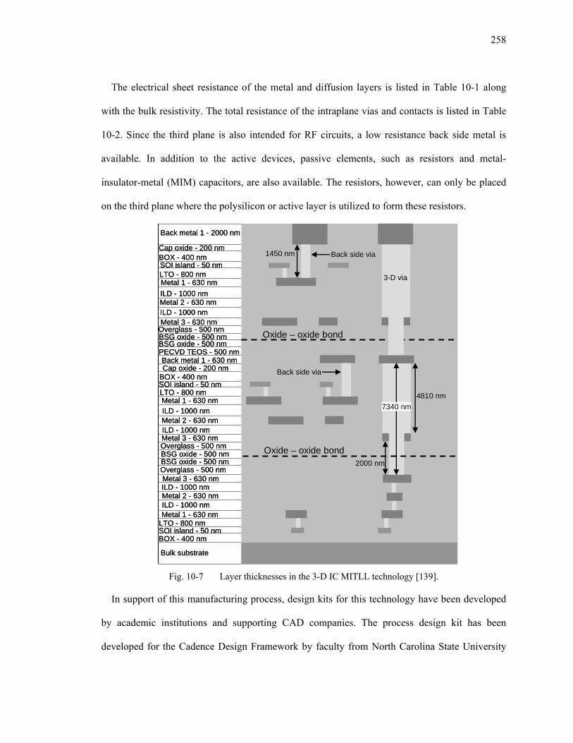
258
The electrical sheet resistance of the metal and diffusion layers is listed in Table 10-1 along
with the bulk resistivity. The total resistance of the intraplane vias and contacts is listed in Table
10-2. Since the third plane is also intended for RF circuits, a low resistance back side metal is
available. In addition to the active devices, passive elements, such as resistors and metal-
insulator-metal (MIM) capacitors, are also available. The resistors, however, can only be placed
on the third plane where the polysilicon or active layer is utilized to form these resistors.
BOX - 400 nmSOI island - 50 nmLTO - 800 nmMetal 1 - 630 nmILD - 1000 nmMetal 2 - 630 nmILD - 1000 nmMetal 3 - 630 nm
Overglass - 500 nmBSG oxide - 500 nmBSG oxide - 500 nmOverglass - 500 nm
BOX - 400 nmSOI island - 50 nmLTO - 800 nmMetal 1 - 630 nmILD - 1000 nmMetal 2 - 630 nmILD - 1000 nmMetal 3 - 630 nm
Cap oxide - 200 nmBack metal 1 - 630 nm
PECVD TEOS - 500 nmBSG oxide - 500 nmBSG oxide - 500 nmOverglass - 500 nmMetal 3 - 630 nm
Metal 1 - 630 nmILD - 1000 nmMetal 2 - 630 nmILD - 1000 nm
BOX - 400 nmSOI island - 50 nmLTO - 800 nm
Cap oxide - 200 nm
Back metal 1 - 2000 nm
Bulk substrate
Oxide – oxide bond2000 nm
4810 nm7340 nm
Back side via
Back side via
3-D via
1450 nm
Oxide – oxide bond
BOX - 400 nmSOI island - 50 nmLTO - 800 nmMetal 1 - 630 nmILD - 1000 nmMetal 2 - 630 nmILD - 1000 nmMetal 3 - 630 nm
Overglass - 500 nmBSG oxide - 500 nmBSG oxide - 500 nmOverglass - 500 nm
BOX - 400 nmSOI island - 50 nmLTO - 800 nmMetal 1 - 630 nmILD - 1000 nmMetal 2 - 630 nmILD - 1000 nmMetal 3 - 630 nm
Cap oxide - 200 nmBack metal 1 - 630 nm
PECVD TEOS - 500 nmBSG oxide - 500 nmBSG oxide - 500 nmOverglass - 500 nmMetal 3 - 630 nm
Metal 1 - 630 nmILD - 1000 nmMetal 2 - 630 nmILD - 1000 nm
BOX - 400 nmSOI island - 50 nmLTO - 800 nm
Cap oxide - 200 nm
Back metal 1 - 2000 nm
Bulk substrate
Oxide – oxide bond2000 nm
4810 nm7340 nm
Back side via
Back side via
3-D via
1450 nm
Oxide – oxide bond
Fig. 10-7 Layer thicknesses in the 3-D IC MITLL technology [139].
In support of this manufacturing process, design kits for this technology have been developed
by academic institutions and supporting CAD companies. The process design kit has been
developed for the Cadence Design Framework by faculty from North Carolina State University

259
[187]. This kit includes device models for circuit simulation and a sophisticated layout tool for 3-
D circuits. For example, circuits located on a specific plane can be separately visualized or
highlighted. In addition, a circuit designed for one plane can be reproduced or transferred to
another plane. Complete design rule checking and circuit extraction are also available. Electrical
rule checking, however, is not included, meaning that these 3-D circuits cannot be directly
checked for shorts between the power and ground lines. However, to mitigate this problem, two
pins can be assigned different names on the power and ground lines. Design rule checking reports
errors whenever lines with different names are crossed, thereby checking for electrical shorts.
TABLE 10-1 LAYER RESISTANCES OF THE 3-D FDSOI PROCESS [139].
Parameter Value Bulk resistivity ~2000 Ω-cm
Silicided n+/p+ active sheet resistance 15 ± 3 Ω/sq Silicided n+/p+ polysilicon sheet resistance 15 ± 3 Ω/sq
Silicided n+/p+ sheet resistance 15 ± 3 Ω/sq Lower metal layer sheet resistance ~0.12 Ω/sq
Top metal layer sheet resistance ~0.08 Ω/sq Back side metal sheet resistance ~0.12 Ω/sq
TABLE 10-2 CONTACT AND VIA RESISTANCES OF THE 3-D FDSOI PROCESS [139].
Parameter Value Poly contact (250 nm × 250 nm) 10 ± 2 Ω
n+ active contact (250 nm × 250 nm) 10 ± 2 Ω p+ active contact (250 nm × 250 nm) 10 ± 2 Ω
Interconnect metal via (300 nm × 300 nm) 4 Ω Backside metal via (500 nm × 500 nm) 2 Ω
10.2. 3-D Circuit Architecture
A test circuit exploring a variety of clock network topologies suitable for 3-D ICs has been
designed based on the process described in the previous section. A block diagram of the design is
depicted in Fig. 10-8. The test circuit consists of four blocks. Each block contains the same logic
circuit but implements a different clock distribution network. The total area of the test circuit is 3
mm × 3 mm. The logic circuit common to all of these blocks is described in this section while the
various clock network topologies are discussed in Section 10.3.
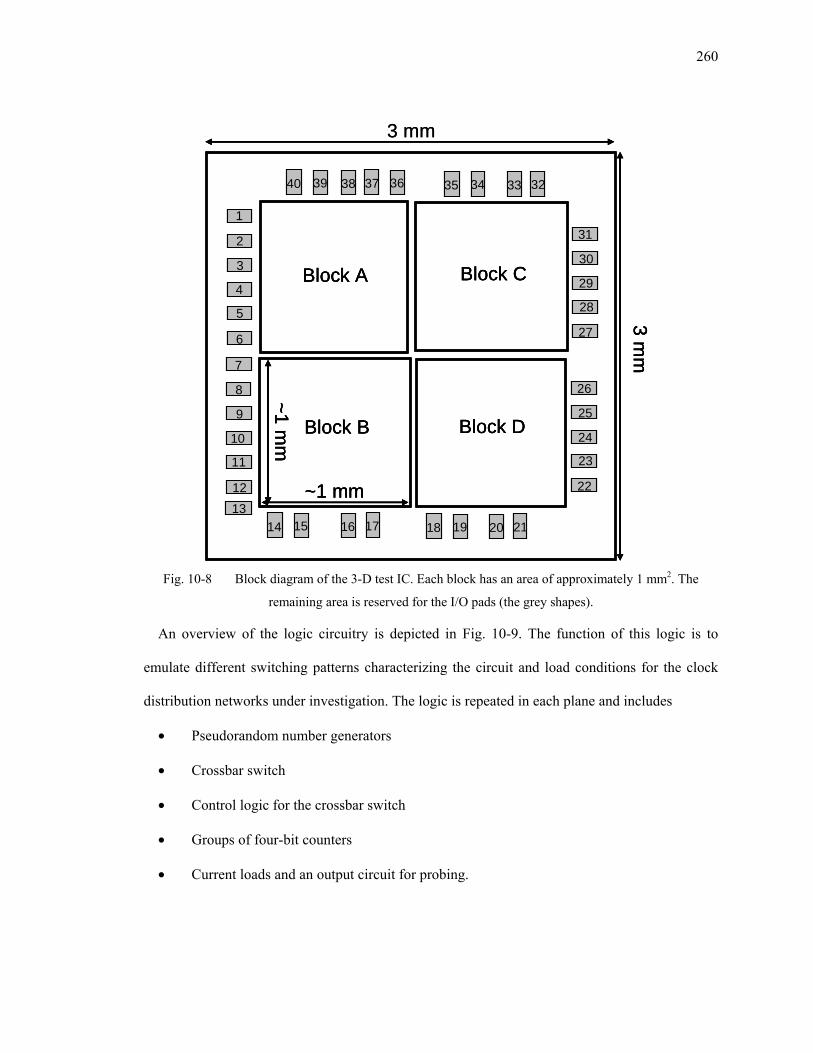
260
3 mm
3 mm
Block DBlock B
Block A
~1 mm
~1 mm
1
2
3
4
5
6
7
8
9
10
11
1213
14 15 16 17 18 19 20 21
35 34 33 32
26
25
24
23
22
31
30
29
28
27
40 39 38 37 36
Block C
3 mm
3 mm
Block DBlock B
Block A
~1 mm
~1 mm
1
2
3
4
5
6
7
8
9
10
11
1213
14 15 16 17 18 19 20 21
35 34 33 32
26
25
24
23
22
31
30
29
28
27
40 39 38 37 36
Block C
3 mm
Block DBlock B
Block A
~1 mm
~1 mm
1
2
3
4
5
6
1
2
3
4
5
6
7
8
9
10
11
1213
14 15 16 17 18 19 20 21
35 34 33 32
26
25
24
23
22
26
25
24
23
22
31
30
29
28
27
31
30
29
28
27
40 39 38 37 36
Block C
Fig. 10-8 Block diagram of the 3-D test IC. Each block has an area of approximately 1 mm2. The
remaining area is reserved for the I/O pads (the grey shapes).
An overview of the logic circuitry is depicted in Fig. 10-9. The function of this logic is to
emulate different switching patterns characterizing the circuit and load conditions for the clock
distribution networks under investigation. The logic is repeated in each plane and includes
• Pseudorandom number generators
• Crossbar switch
• Control logic for the crossbar switch
• Groups of four-bit counters
• Current loads and an output circuit for probing.

261
The pseudorandom generators are based on the technique described in [282], which uses linear
feedback shift registers and XOR operations to generate a random 16-bit word every clock cycle
after the first few cycles required to initialize the generator. The physical layout of one random
number generator is illustrated in Fig. 10-10. There are a total of nine pseudorandom generators
in each circuit block, connected by groups of three to the crossbar switch within each plane.
PN
G A 6 x 6
CrossbarSwitch
4x4-
bit c
ount
ers
4 gr
oups
of c
urre
nt
load
s
Control Logic
16 16
PN
G B
PN
G C
6x16
Fig. 10-9 Block diagram of the logic circuit included in each plane of each block.
Fig. 10-10 Physical layout of a pseudorandom number generator.
A classic crossbar switch with six input and output ports is included in each plane, where the
width of each port is 16 bits. Three of the six inputs of the crossbar switch are connected to the
output of the number generators, while the remaining inputs are connected to ground. The
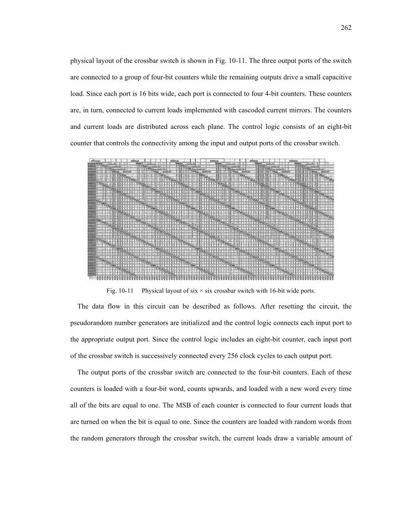
262
physical layout of the crossbar switch is shown in Fig. 10-11. The three output ports of the switch
are connected to a group of four-bit counters while the remaining outputs drive a small capacitive
load. Since each port is 16 bits wide, each port is connected to four 4-bit counters. These counters
are, in turn, connected to current loads implemented with cascoded current mirrors. The counters
and current loads are distributed across each plane. The control logic consists of an eight-bit
counter that controls the connectivity among the input and output ports of the crossbar switch.
Fig. 10-11 Physical layout of six × six crossbar switch with 16-bit wide ports.
The data flow in this circuit can be described as follows. After resetting the circuit, the
pseudorandom number generators are initialized and the control logic connects each input port to
the appropriate output port. Since the control logic includes an eight-bit counter, each input port
of the crossbar switch is successively connected every 256 clock cycles to each output port.
The output ports of the crossbar switch are connected to the four-bit counters. Each of these
counters is loaded with a four-bit word, counts upwards, and loaded with a new word every time
all of the bits are equal to one. The MSB of each counter is connected to four current loads that
are turned on when the bit is equal to one. Since the counters are loaded with random words from
the random generators through the crossbar switch, the current loads draw a variable amount of

263
current during circuit operation. This randomness is used to mimic different switching patterns
that can exist within a circuit.
The current loads are implemented with cascoded current mirrors, as shown in Fig. 10-12. In
the cascoded current mirrors, the output current Iout closely follows Iref as compared to a simple
current mirror. The reference current Iref is externally provided to control the amount of current
drawn from the circuit. The gate of transistor M5 is connected to the MSB of a four-bit counter,
shown in Fig. 10-12 as the sel signal. This additional device is used to switch the current sinks.
The layout of a group of four current loads is illustrated in Fig. 10-13. The width of the devices
shown in Fig. 10-12 is
nm2000nm,600 54321 ===== WWWWW . (10-1)
The power supply is 1.5 volts, as set by the MITLL process.
Iref
Iout
M1 M2
M3 M4
sel M5Iref
Iout
M1 M2
M3 M4
sel M5
Fig. 10-12 Cascoded current mirror with an additional control transistor.
The final layout of the test circuit is illustrated in Fig. 10-14, while the connectivity of the pads
to the external signals is listed in Table 10-3. Several decoupling capacitors are included in each
circuit block and are highlighted in Fig. 10-14. The capacitors serve as extrinsic decoupling
capacitance and are implemented by MIM capacitors. Note that the number of pads is not limited
by the area of the circuit but rather by the maximum number of connections permitted by the

264
available probe card. The backside metal layer of the third plane is utilized for the pads. Each of
the circuit blocks is supplied by separate power and ground pads, while only a pair of power and
ground pads is connected to the pad ring to provide protection from electrostatic discharge.
Fig. 10-13 Four stage cascoded current mirrors.
10.3. Clock Signal Distribution in 3-D Circuits
Different clock distribution network architectures for 3-D circuits are investigated in this section.
Fundamental concepts for the timing of synchronous systems are introduced. Some design issues
related to distributing a clock signal in synchronous circuits are also discussed in Section 10.3.1.
The clock networks employed in each of the blocks within the test circuit are described in Section
10.3.2.
10.3.1. Timing Characteristics of Synchronous Circuits
In synchronous circuits, the clock signal provides a common time reference for all of the
sequential elements, orchestrating the flow of the data signals within a circuit [277]. A number of
clock network topologies have been developed for 2-D circuits which can be symmetric, such as
H- and X-trees, highly asymmetric, such as buffered tress and serpentine shaped structures [283],
[284], and grid like structures, such as rings and meshes. The clock distribution network is

265
structured as a global network with multiple smaller local networks. With the global clock
network, the clock signal is distributed to specific locations across the circuit. These locations are
the source of the local networks that pass the clock signal to the registers or other storage
elements.
Block A
Block B
Block C
Block D
RF pad
Decap
Decap
Decap
Block A
Block B
Block C
Block D
RF pad
Decap
Decap
Decap
Fig. 10-14 Physical layout of the test circuit. Some decoupling capacitors are highlighted.
A symmetric structure such as an H-tree is often utilized in global clock networks [284], as
shown in Fig. 10-15. The most attractive characteristic of symmetric structures is that the clock
signal ideally arrives simultaneously at each leaf of the clock tree. Due to several reasons,
however, such as load imbalances, process variations, and crosstalk, the arrival time of the clock
signal at various locations within a symmetric tree can be different, producing clock skew. More
precisely, clock skew is defined as the difference between the clock signal arrival time of

266
sequentially-adjacent registers [284]. Two registers are sequentially-adjacent if these registers are
connected with combinatorial logic (i.e., no additional registers intervene between sequentially-
adjacent registers). An illustration of this data path is provided in Fig. 10-16. An expression for
the clock skew Tskew between these registers is also shown in Fig. 10-16, where iCT and CjT are
the arrival time of the clock signal at register Ri and Rj, respectively.
TABLE 10-3 PAD CONNECTIVITY OF THE 3-D TEST CIRCUIT (PAD INDEX SHOWN IN FIG. 10-8).
Index Pad connectivity Index Pad connectivity 1 reset 21 reset 2 Vdd 22 Vss 3 Vss 23 Vdd 4 Output bit 24 Output bit 5 Vss 25 Vdd 6 Vdd 26 Vss 7 Output bit 27 Vss 8 reset 28 Vdd 9 Vss 29 Iref10 Vdd 30 Vss 11 Iref 31 Vdd 12 Vss 32 reset 13 Vdd 33 Vdd 14 Vdd 34 Vss 15 Vss 35 Output bit 16 Vdd 36 Vss 17 Vss 37 Vdd 18 Iref 38 Iref19 Vdd 39 Vss 20 Vss 40 Vdd
The clock signal typically traverses long distances to reach every sequential element within a
circuit. In symmetric structures, such as H-trees, the traversed distances are often longer to
preserve symmetry. Due to these extremely long interconnects and higher clock frequencies, the
clock network is typically modeled as a transmission line, since inductive behavior is likely to
occur [268]. Such behavior can cause multiple reflections at the branch points, directly affecting
the performance and power consumed by the clock network. In order to lessen the reflections at
the branch points of the tree, the interconnect width of the segments at each branch point is
halved (for a 2× change in the line width) to ensure that the total impedance seen at that branch
point is maintained constant (matched impedance).

267
Clock driver
1
2 2
3 3
3 3
4 4 4 4
4 4 4 4
Fig. 10-15 Two-dimensional four level H-tree.
10.3.2. Clock Distribution Network Structures within the Test Circuit
Different clock distribution schemes for 3-D circuits are described in this subsection. To evaluate
the specific requirements of the clock networks, consider a traditional H-tree topology. As shown
in Fig. 10-15, at each branch point of an H-tree, two branches emanate with the same length. An
extension of the H-tree to three dimensions does not guarantee equidistant interconnect paths
from the source to the leaves of the tree. This situation is shown in Fig. 10-17, where an H-tree is
replicated in each plane of a 3-D circuit. The clock signal is propagated through interplane vias
from the output of the clock driver to the center of the H-tree on planes one and three. The
impedance of these vias increases the time for the clock signal to arrive at the leaves of the tree
on these planes as compared to the time for the clock signal to arrive at the leaves of the tree on
the same plane as the clock driver. Furthermore, in a multi-plane 3-D circuit, three or four
branches can emanate from each branch point. The third branch propagates the clock signal to the
other planes of the 3-D circuit, as shown in Fig. 10-17. Similar to a design methodology for a 2-D
H-tree topology, the width of each branch is reduced to a third (or more) of the segment

268
preceding the branch point in order to match the impedance at the branch point. This requirement,
however, is difficult to achieve as the third and fourth branch are connected by an interplane via.
The vertical interconnects are of significantly different length as compared to the horizontal
branches and also exhibit different impedance characteristics.
Data register
Ri
Data register
Rj
Ci Cj
Clock input Clock input
Data Input
Data Output
ji CCskew TTT −=
Combinatorial logicData
register
Ri
Data register
Ri
Data register
Rj
Data register
Rj
Ci Cj
Clock input Clock input
Data Input
Data Output
ji CCskew TTT −=
Combinatorial logic
Fig. 10-16 A data path depicting a pair of sequentially-adjacent registers.
1st plane
2nd plane
3rd plane
1st plane
2nd plane
3rd plane
Fig. 10-17 Two-dimensional H-trees constituting a clock distribution network for a 3-D IC.
Various clock network topologies for 3-D ICs are investigated in this case study. Each of the
four blocks of the test circuit includes a different clock distribution structure, which are
schematically illustrated in Fig. 10-18. The physical layout of these topologies for the MITLL 3-
D technology is depicted in Fig. 10-19. The architectures employed in the blocks are:
Block A: All of the planes contain a four level H-tree (i.e., equivalent to 16 leaves) with
identical interconnect characteristics. The H-trees are connected through a group
of interplane vias, as shown in Fig. 10-18a. The second plane is front-to-front

269
bonded with the first plane and both of the H-trees are implemented on the third
metal (M3) layer. The physical distance between these clock networks is
approximately 2 µm. Note that the H-tree on the second plane is rotated by 90o
with respect to the H-trees on the other two planes. The orthogonal placement of
these two clock networks effectively eliminates the inductive coupling. All of the
H-trees are shielded with two parallel lines connected to ground.
Block B: A four level H-tree is included in the second plane. Each of the leaves of this H-
tree is connected through interplane vias to small local rings on the first and
second plane, as illustrated in Fig. 10-18b. As in Block A, the H-tree is shielded
with two parallel lines connected to ground. Additional interconnect resources
are used to form local meshes. Due to the limited interconnect resources,
however, a uniform mesh in each ring is difficult to achieve. The clock routing is
constrained by the power and ground lines as only three metal layers are
available on each plane.
Block C: The clock distribution network for the second plane is a shielded four level H-
tree. Two global rings are utilized for the other two planes, as depicted in Fig.
10-18c. Each ring is connected through interplane vias to the four branch points
on the second level of the H-tree. The registers in each plane are individually
connected to the ring.
Block D: The clock network on each plane consists of a trunk structure and branches that
connect the registers in each plane to the trunk, as shown in Fig. 10-18d. As for
Block A, the trunk for the second plane is rotated by 90o to avoid inductive
coupling. Those interconnects that branch from the trunk are placed as close as
possible to the registers.

270
1st plane
2nd plane
3rd plane
1st plane
2nd plane
3rd plane
Local clocknetworks
1st plane
2nd plane
3rd plane
1st plane
2nd plane
3rd plane(a) (b)
(c) (d)
Fig. 10-18 Various 3-D clock distribution networks within the test circuit, (a) H-trees, (b) H-tree and
local rings/meshes, (c) H-tree and global rings, and (d) trunk based.
Buffers are inserted at appropriate branch points within the H-trees to amplify the clock signal.
In each of the circuit blocks, the clock driver for the entire clock network is located on the second
plane. The clock driver on that plane is placed to ensure that the clock signal propagates through
similar vertical interconnect paths to the first and third plane, resulting in the same effective delay
for the registers located on the first and third planes. The clock driver is implemented with a
traditional chain of tapered buffers [285]-[287].
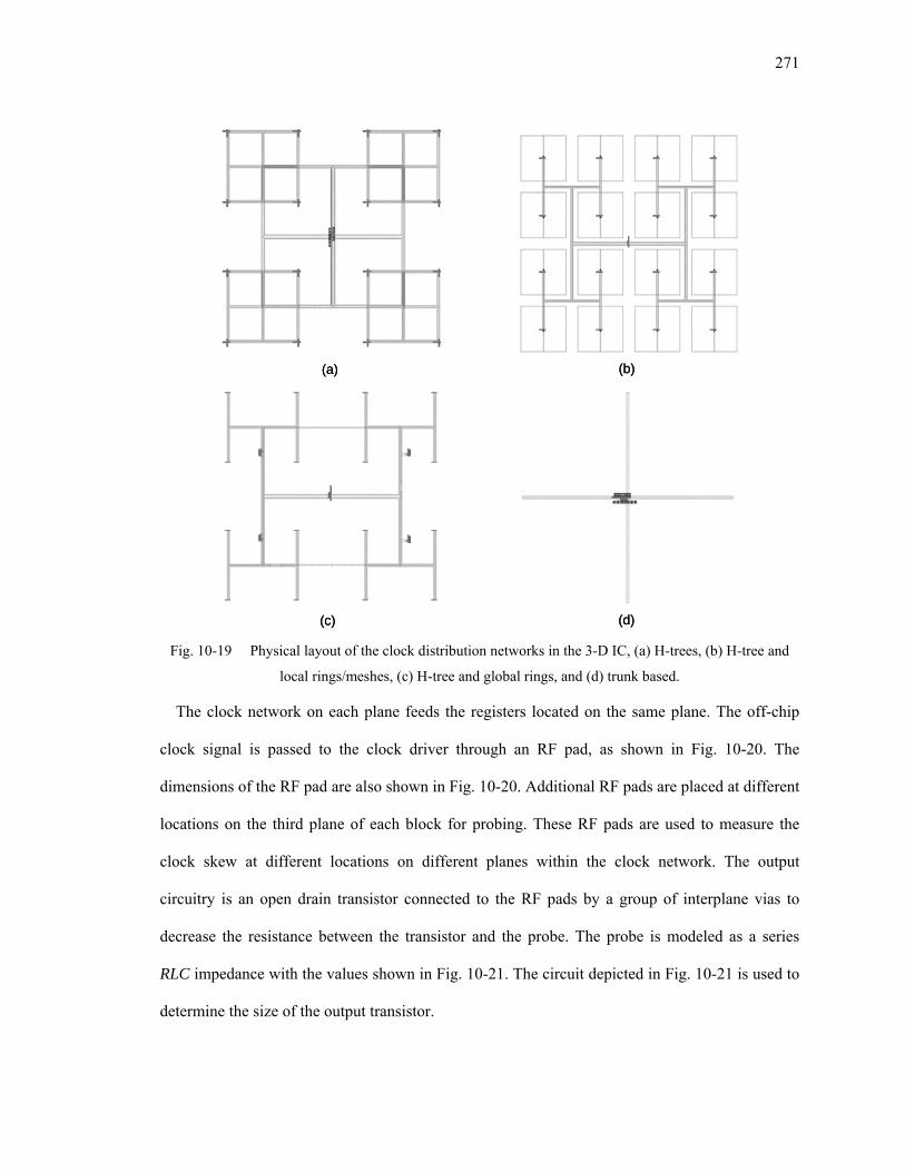
271
(c) (d)
(a) (b)
(c) (d)
(a) (b)
Fig. 10-19 Physical layout of the clock distribution networks in the 3-D IC, (a) H-trees, (b) H-tree and
local rings/meshes, (c) H-tree and global rings, and (d) trunk based.
The clock network on each plane feeds the registers located on the same plane. The off-chip
clock signal is passed to the clock driver through an RF pad, as shown in Fig. 10-20. The
dimensions of the RF pad are also shown in Fig. 10-20. Additional RF pads are placed at different
locations on the third plane of each block for probing. These RF pads are used to measure the
clock skew at different locations on different planes within the clock network. The output
circuitry is an open drain transistor connected to the RF pads by a group of interplane vias to
decrease the resistance between the transistor and the probe. The probe is modeled as a series
RLC impedance with the values shown in Fig. 10-21. The circuit depicted in Fig. 10-21 is used to
determine the size of the output transistor.

272
Block i
RF pad
Clock Input
Clock outputs
G GS
100 µm70 µm Block i
RF pad
Clock Input
Clock outputs
G GS
100 µm70 µm
Fig. 10-20 Clock signal probes with RF pads.
In addition to the clock skew of the clock network topologies employed within the blocks of
the test circuit, the power consumption of the entire clock distribution network has also been
measured. Since all of the blocks include the same logic circuits, any difference in power
consumption is attributed to the clock network, including the interconnect structures, clock driver,
and clock buffers. The measurements of the clock skew and power dissipation of the blocks are
discussed in the following section.
Vdd
R
C nF
L m
clk
Vdd
R
C nF
L m
clk
Fig. 10-21 Open drain transistor and circuit model of the probe.

273
10.4. Experimental Results
The clock distribution network topologies of the 3-D test circuit are evaluated in this section. The
fabricated circuit is depicted in Fig. 10-22, where the four individual blocks can be distinguished.
A magnified view of one block is shown in Fig. 10-23. Each block includes four RF pads for
measuring the delay of the clock signal. The pad located at the center of each block provides the
input clock signal. The clock input is a sinusoidal signal with a DC offset, which is converted to a
square waveform at the output of the clock driver. The remaining three RF pads are used to
measure the delay of the clock signal at specific points on the clock distribution network within
each plane. A buffer is connected to each of these measurement points. The output of this buffer
drives the gate of an open drain transistor connected to the RF pad. The RF probes landing on
these pads are depicted in Fig. 10-24, where the die assembly on the probe station is illustrated.
Fig. 10-22 Top view of the fabricated 3-D test circuit.
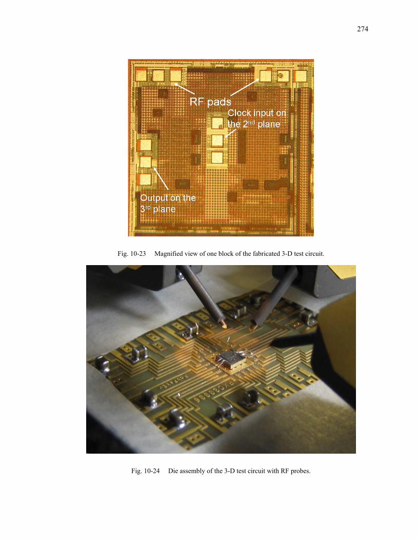
274
Fig. 10-23 Magnified view of one block of the fabricated 3-D test circuit.
Fig. 10-24 Die assembly of the 3-D test circuit with RF probes.

275
A clock waveform acquired from the topology combining an H-tree and global rings, shown in
Fig. 10-18c, is illustrated in Fig. 10-25, demonstrating operation of the circuit at 1.4 GHz. The
clock skew between the planes of each block is listed in Table 10-4. The topologies are ordered in
Fig. 10-26 in terms of the maximum measured clock skew between two planes. The delay of the
clock signal from the RF input pad at the center of each block to the measurement point on plane
i is denoted as TCi in Table 10-4. For example, TCA denotes the delay of the clock signal to the
measurement point on plane A. Additionally, the difference in the delay of the clock signal
between two measurements points on planes i and j is notated as TCi-j.
For the H-tree topology, the clock signal delay is measured from the root to a leaf of the tree on
each plane, with no other load connected to these leaves. The skew between the leaves of the H-
tree on planes A and C (i.e., TCA-C) is effectively the delay of a stacked 3-D via traversing the
three planes to transfer the clock signal from the target leaf to the RF pad on the third plane. The
delay of the clock signal to the sink of the H-tree on the second plane TCB is larger due to the
additional capacitance within that quadrant of the H-tree. This capacitance is intentional on-chip
decoupling capacitance placed under the quadrant, increasing the measured skew of TCB-C and
TCB-A. This topology produces, on average, the lowest skew as compared to the two other
topologies.
Fig. 10-25 Clock signal input and output waveform from the topology illustrated in Fig. 10-18c.

276
Topology
Max
imum
clo
ck s
kew
[ps]
130.6 ps
68.4 ps
32.5 ps
Fig. 10-26 Maximum measured clock skew between two planes within the different clock distribution
networks.
In the H-tree topology, each leaf of a tree is connected to registers located only within the same
plane. Allowing one sink of an H-tree to drive a register on another plane adds the delay of
another 3-D via to the clock signal path, further increasing the delay. Consequently, the registers
within each plane are connected to the H-tree on the same plane. Note that this approach does not
imply that these registers only belong to data paths contained within the same plane.
TABLE 10-4 MEASURED CLOCK SKEW AMONG THE PLANES OF EACH BLOCK.
Clock distribution network Clock skew [ps] TC
(B-A) = TCB
- TCATC(B-C)
= TCB - TCC
TC(A-C) = TCA
- TCC
H-trees (Fig. 10-18a) 32.5 28.3 -4.2 Local meshes (Fig. 10-18b) -68.4 -18.5 49.8 Global rings (Fig. 10-18c) -112.0 -130.6 -18.6
The clock skew among the planes is greater for the local mesh topology as compared to the H-
tree topology, primarily due to the imbalance in the clock load for certain local meshes. Indeed,
this topology has only 16 tap points within the global clock distribution network; three times
fewer than the H-tree topology illustrated in Fig. 10-18a. This difference can produce a

277
considerable load imbalance, greatly increasing the local clock skew as compared to the local
clock skew within the H-tree topology. By inserting the local meshes on planes A and C, which
are connected to the 16 sinks of the H-tree on the second plane, the local clock skew is smaller.
The greatest difference in the load is between the measurement points on planes A and B, which
also produces the largest skew for this topology. The increase in skew, however, as compared to
the H-tree topology, is moderate.
Consequently, a limitation of the local meshes topology is that greater effort is required to
control the local skew. The fewer number of sinks driven by the global clock distribution network
increases the number of registers clocked by each sink. To better explain this situation, consider a
segment of each topology shown in Figs. 10-27a and 10-27b, respectively. For the H-tree
topology, the clock signal is distributed from three sinks, one on each plane, to the registers
within the circular area depicted in Fig. 10-27a. Note that the radius of the circle on planes A and
C is slightly smaller to compensate for the additional delay of the clock signal caused by the
impedance characteristics of the 3-D vias. The registers located within these regions satisfy
specific local skew constraints. Alternatively, in the case of the local mesh topology, the clock
signal at the sinks of the H-tree on the second plane feeds registers in each of the three planes.
Consequently, each sink of the tree connects to a larger number of registers as compared to the H-
tree topology, as depicted by the shaded region in Fig. 10-27b. Despite the beneficial effect of the
local meshes, load imbalances are more pronounced for this topology. Alternatively, the H-tree
topology (see Fig. 10-18a) utilizes a significant amount of interconnect resources, dissipating
more power.
The clock distribution network with the global rings exhibits low skew for planes A and C,
those planes that include the global rings. The objective of this topology is to evaluate the
effectiveness of a less symmetric architecture in distributing the clock signal within a 3-D circuit.

278
Although the clock load on each ring is non-uniformly distributed, the load balancing
characteristic of the rings yields a relatively low skew between the planes. Since the clock
distribution network on the second plane is implemented with an H-tree, the skew between
adjacent planes is significantly larger than the skew between the top and bottom planes. Note that
the sinks of the H-tree are located at a great distance from the rings on planes A and C (see Fig.
10-18c). A combination of H-tree and global rings, consequently, is not a suitable approach for 3-
D circuits due to the difficulty in matching the distance that the clock signal traverses on each
plane from the sink of the tree or the ring to the many registers distributed across a plane.
(a) (b)
Fig. 10-27 Part of the clock distribution networks illustrated in Figs. 10-18a and 10-18b. (a) The local
clock skew is individually adjusted within each plane for the H-tree topology and (b) the local skew is
simultaneously adjusted for all of the planes for the local mesh topology.
The measured power consumption of the blocks operating at 1 GHz is reported in Table 10-5.
An ordering of the blocks in terms of the measured dissipated power is illustrated in Fig. 10-28.
The local mesh topology dissipates the lowest power. This topology requires the least
interconnect resources for the global clock network, since the local meshes are connected at the
output of the buffers located on the last level of the H-tree on the second plane. In addition, this
topology requires a small amount of local interconnect resources as compared to the H-tree and
global rings topologies. Most of the registers are connected directly to the local rings.

279
Alternatively, the power consumed by the H-tree topology is the highest, as this topology requires
three H-trees and additional wiring for the local connections to the leaves of each tree. In
addition, the greatest number of buffers is included in this topology. This number is threefold as
compared to the number of buffers used for the local mesh topology. Finally, the global rings
block consumes slightly less power than the H-tree topology due to the reduced amount of wiring
resources used by the global clock network.
TABLE 10-5 MEASURED POWER CONSUMPTION OF EACH BLOCK OPERATING AT 1 GHZ.
Clock distribution network Power consumption [mW] H-trees (Fig. 10-18a) 260.3
Local meshes (Fig. 10-18b) 168.3 Global rings (Fig. 10-18c) 228.5
Topology
Pow
er c
onsu
mpt
ion
@ 1
GH
z [m
W]
228.5 mW
168.3 mW
260.5 mW
Fig. 10-28 Measured power consumption at 1 GHz of the different circuit blocks.
Although the local mesh topology requires the least interconnect resources, a large number of
3-D vias is required for the interplane connections. Since the 3-D vias block all of the metal
layers and occupy silicon area, the routing blockage increases considerably as compared to the H-

280
tree topology. The global rings topology requires a moderate number of 3-D vias as only four
connections between the vertices of the rings and the branch points of the H-tree are necessary.
Since three-dimensional integration greatly increases the complexity of designing a
synchronization system, a topology that offers low overhead in the design process of a 3-D clock
distribution network is preferable. From this perspective, a potential advantage of the H-tree
topology is that each plane can be individually analyzed. This behavior occurs in an H-tree
topology since the clock distribution network in each plane is exclusively connected to registers
within the same plane. Alternatively, in the local ring topology, all of the registers from all of the
planes, which are connected to each sink of the tree on the second plane, need to be
simultaneously considered.
10.5. Summary
A case study for investigating several clock distribution networks for 3-D ICs has been described
in this chapter and measurements from a 3-D test circuit have been presented. The characteristics
of the circuit and related topologies are:
• A 3-D clock distribution network cannot be directly extended from a 2-D circuit due to
the lack of symmetry in a 3-D circuit due to the effect of the interplane vias.
• The 3-D FDSOI fabrication technology from MITLL has been used to manufacture the
test circuit.
• The 3-D test circuit is composed of four independent blocks, where each block is a three
plane 3-D circuit. For each block, a different clock distribution network is utilized.
• All of the blocks in each plane share the same logic circuitry to emulate a variety of
switching patterns in a synchronous digital circuit.
• The maximum clock frequency of the fabricated 3-D test circuit is 1.4 GHz.

281
• A comparison of the clock skew and power consumption of each block is provided. A
topology combining the symmetry of an H-tree on the second plane and local meshes on
the other two planes results in low clock skew for 3-D circuits while consuming the
lowest power as compared to the other investigated topologies.

282
Chapter 11. Conclusions
With MOSFET channel lengths several tens of nanometers long, modern silicon integrated
systems can support gigascale transistor densities. On-chip systems, for example, often include
several processing cores within a microprocessor system or a mixture of various silicon
technologies, such as analog, digital, and RF, in a mixed-signal SoC. The former is the heart of a
high performance computing system while the latter can feature a versatile, compact, and portable
electronic product. A fundamental requirement for this system-on-chip paradigm is efficient and
reliable communication among the system components.
High speed, low power, and low noise inter-component communication is fundamentally
limited by the increasing impedance characteristics and length of the interconnect. Three-
dimensional integration is a revolutionary solution to the deleterious effects of the long
interconnects. In vertically integrated systems, the long interconnects spanning several
millimeters are replaced by orders of magnitude shorter vertical wires. This inherent reduction in
wirelength provides opportunities for increased speed, enhanced noise margins, and lower power.
Three-dimensional integrated systems can also comprise a variety of different silicon
technologies, such as digital, analog, RF CMOS and SOI circuits, and non-silicon semiconductor
technologies, such as SiGe and GaAs, making 3-D systems highly suitable for a broad spectrum
of applications. This salient characteristic raises a greater interest in three-dimensional integration
as compared to other incremental solutions that simply scale CMOS technologies.
Within the context of an electronic product, circuit level enhancements can profoundly affect
fundamental system requirements, such as compactness, portability, and computing power. Since
the application space for these systems is broad, a plethora of 3-D technologies are under
development. These approaches range from monolithic 3-D circuits to polylithic and

283
heterogeneous multi-plane systems. The fundamental element of a 3-D silicon system can be a
single transistor, a functional block, a bare die, or a packaged circuit. The structural granularity of
the system, in turn, determines the form of vertical interconnections, which link the elements of a
3-D circuit in the vertical direction. The cost of manufacturing is directly related to the processing
capabilities offered by these technologies. Fabrication processes that utilize TSVs for vertical
interconnects are an economic form of vertical integration, while exhibiting considerable
improvement in system performance.
A major outcome of this dissertation is that effective solutions to physical design issues for 3-D
circuits are demonstrated, emphasizing the significance of the TSVs. In the 3-D design process,
the through silicon vias should be treated as a means to improve signaling among the physical
planes within a 3-D stack.
The TSVs in a 3-D circuit provide synchronization, power and ground, and signaling among
the planes and – in contrast to mainstream 2-D circuits – thermal cooling. The primary challenges
and novel solutions for satisfying these objectives have been presented throughout the
dissertation.
The electrical characteristics of the TSVs affect all but the thermal objective. Consequently, the
impedance characteristics of the TSVs structures are considered in design algorithms and
techniques to improve signaling. These methods enhance the benefits provided by the shorter
interconnect length. The effectiveness of physical design techniques is considerably improved by
exploiting the electrical behavior of these vias. This behavior is investigated in the case study of a
fabricated 3-D circuit that evaluates the important issue of synchronization; a crucial objective in
global signaling. Different ways to efficiently distribute the clock signal in the gigahertz regime
are explored temporally and within three spatial dimensions for the first time. In a nutshell,

284
enhanced interplane signaling is a prerequisite for high performance and/or high bandwidth 3-D
computing applications.
High performance applications typically include communications limited architectures, such as
a processor-memory system. Communication fabrics, such as on-chip networks and FPGAs, also
greatly benefit from the short vertical interconnects. Different architectural configurations are
explored in this dissertation, demonstrating the many possible power and latency tradeoffs that
result from exploiting the third dimension. Appropriate latency and power models supporting this
analysis are also presented.
Finally, a systematic approach is provided for inserting and distributing the vertical
interconnects to improve the overall thermal conductivity of a 3-D stack. By including the
thermal objective in 3-D physical design algorithms and techniques, thermal gradients and high
temperatures, which can degrade the reliability and performance of a 3-D circuit, are significantly
reduced. Due to the high power densities, the thermal objective is an integral part of the physical
design process for 3-D integrated systems. Presently, the lack of advanced packaging has shifted
the focus of removing heat to primarily on-chip solutions. Design methodologies for circuit and
package thermal co-design will offer superior solutions due to the high temperatures within 3-D
circuits.
The major achievement of this dissertation is the thorough exploration of multiple aspects of
three-dimensional integration from manufacturing to physical design and algorithms to system
level architectures. This comprehensive approach targets the design and analysis of 3-D
integration from a circuits perspective. With this point of view, the primary objective in the
development of this dissertation is to provide intuition behind the most sensitive issues regarding
the vertical interconnect, which is essentially intertwined within each step of the 3-D design
process. The material described in this thesis is intended to shed light on those areas related to the

285
design of 3-D integrated systems in an effort to develop large scale multi-functional multi-plane
systems to continue the microelectronics revolution.

286
Chapter 12. Future Work
Various challenges to 3-D integration have been comprehensively discussed throughout this
dissertation. Open research problems related to both manufacturing technologies for 3-D circuits
and related physical design techniques and algorithms require further investigation. A profound
need exists for 3-D design methodologies, which currently are in an embryonic stage. For
instance, global signaling and signal integrity issues in 3-D circuits have yet to be investigated.
More specifically, the problem of distributing abundant power to every transistor in each plane,
within a diverse and complex 3-D system, is critical. A variety of power distribution grids is often
used to distribute power within a 2-D circuit. The architecture of these grids is primarily
determined by the target impedance of the power distribution network. In a multi-plane system,
more than one power grid is required. In addition, current is transferred to the planes located far
from the power/ground pads of the package through the vertical interconnects. The voltage droop
caused by these structures needs to be investigated for various 3-D technologies.
As described in Chapter 9, 3-D NoC can improve the performance of traditional on-chip
networks. Several applications implemented by on-chip networks require certain throughput and
quality of service (QoS), for example, audio and video applications. This data traffic can cause
the temperature of some interconnect busses to reach unacceptable levels due to interconnect
joule heating. This situation can result in increased latency while accelerating wear out
mechanisms within a circuit. A possible approach to avoid such problems is to identify those
paths with the higher temperature (i.e., hot paths) and route the data along alternative paths. This
detour, however, should not compromise network bandwidth.
A unique characteristic of 3-D integrated systems is vertical communication, implemented by
vertical interconnect busses in 3-D NoCs. A vertically transmitted signal is typically propagated

287
along a small interconnect length which ranges from several tens to a couple of hundred
micrometers. Despite the shorter interconnect length, shielding is necessary, as a signal in the z-
direction can be surrounded by a large number of signals. For 3-D NoC architectures, signal
integrity becomes a crucial issue, since data are exclusively transferred in the vertical direction
through busses.
Power distribution issues for 3-D ICs are discussed in Section 12.1. Crosstalk among the
vertical interconnects and related shielding approaches are described in Section 12.2. Finally,
thermal-aware packet routing for 3-D NoC is discussed in Section 12.3. A summary of these open
research issues is offered in Section 12.4.
12.1. Power Distribution Networks for 3-D ICs
Distributing power in integrated circuits is an important and highly complex issue. The design of
power distribution networks includes several steps where the information describing the physical
design and the current profile of the circuit blocks are refined at each step of the design process
[288]. A variety of power distribution networks has been developed for different types of circuits.
For high performance systems, such as microprocessors, an architecture consisting of a single or
multiple pair grids is typically used to deliver power to the individual devices. This architecture is
implemented at the global and semi-global metal layers, while short interconnects at the lower
metal layers are used for the power and ground connections within each cell [174]. An example
of a power distribution grid is schematically shown in Fig. 12-1 [289]. Grid architectures produce
sufficiently small output impedances of the power distribution system; however, a significant
amount of wiring resources is required as compared to other simpler but less efficient power
distribution topologies. Different styles of power distribution grids with considerably different
impedance characteristics have also been investigated [290].

288
Implementing a power distribution network for a high performance multi-plane system will
require several grids, one for each physical plane or a mixture of grid-based and other simpler
architectures, such as meshes and star-like structures [174]. Analyzing such a complicated power
distribution system to determine the voltage droop or the impedance of the entire system requires
significant computational capability. A simpler way to approach this problem is to separately
analyze the power distribution network within each plane of the 3-D system. This decoupling is
based on the assumption that each TSV only carries current to the bottom plane connected to the
TSV. This configuration is illustrated in Fig. 12-2. This assumption is reasonable since any other
current path would include a horizontal interconnect segment, resulting in a path with greater
impedance. Techniques that accurately and effectively analyze these complicated structures need
to be developed.
Fig. 12-1 Power distribution grid commonly used in high performance integrated circuits.
Beyond the analysis of power distribution architectures, methodologies for designing these
networks are required. In support of this effort, the impedance characteristics of the TSVs must
be investigated. Additionally, TSVs can block the metal layers within a plane. Consequently,
utilizing an unnecessary large numbers of vias to satisfy voltage droop requirements of each plane
can considerably increase the routing congestion within these planes. The number and placement

289
of the TSVs within the power and ground network should be determined based on the range of
signal frequencies and the current demand within each plane.
A high level strategy to facilitate the design of a power distribution network for 3-D ICs would
be to place the circuit blocks with the highest current demands closer to the face of the package
that contains the I/O pads. In conventional packages, one face of the package is dedicated to the
I/Os while the heat sink is attached to the opposite face. Consequently, placing the high switching
activity blocks on the plane adjacent to the I/Os hinders the heat removal process as the distance
from the heat sink increases. The thermal reliability of the system can be considerably degraded
unless the package provides an advanced cooling mechanism.
Package pads I
II
I = I1 + I2 + I3
I2 + I3
I I
Plane 1
Plane 2
Plane 3
I I
I2 + I3
I2
I1
I3
I3
I3
I1
I3
I2
Fig. 12-2 Decoupling the power distribution networks can reduce the design complexity of the power
delivery task in 3-D ICs. Each power distribution grid is treated as carrying only the amount of current
consumed by the corresponding plane.
Alternatively, placing the circuit blocks with the greatest power dissipation on the physical
plane located closest to the heat sink to enhance the heat removal process further constrains the
design of the power distribution network. These limitations are due to the increase in the physical
distance between the power/ground pads of the package and the power distribution network of the

290
plane. This configuration can violate the power supply noise limits for that plane, resulting in
degraded performance or malfunctioning of the circuit. Furthermore, each of these scenarios
requires a different number of TSVs for the power distribution network in order to lower the
impedance of the network in the z-direction.
Design methodologies for robust power distribution networks of 3-D systems should therefore
consider the thermal profile of the circuit in addition to the density and impedance characteristics
of the TSVs. The increase in the resistivity of the power distribution grids in some of the planes
due to the higher temperatures should also be considered.
12.2. Signal Integrity in the Vertical Direction
There are several mechanisms that can compromise signal integrity in an integrated system.
Crosstalk noise among neighboring signals, for example, can cause spurious transitions or
increase the delay required to transmit a signal. Alternatively, substrate coupling between the
digital and analog part of a mixed-signal circuit can inject noise into the sensitive analog
circuitry. Noise can have a detrimental effect on the operation of analog circuits, such as a
decrease in the gain and bandwidth of the amplifiers or an increase in the phase noise of the
voltage controlled oscillators.
In 3-D mixed-signal circuits, new opportunities emerge for noise mitigation by implementing
the analog and digital portion of the circuit on different physical planes. This configuration can
eliminate substrate coupling and decrease crosstalk noise between the analog and digital circuitry.
Both analog and digital signals can cross multiple planes in a 3-D mixed-signal circuit. Despite
the short vertical interconnects, crosstalk noise can be significant due to the large number of
neighboring signals. Consider, for instance, a buss in the third dimension implemented by TSVs,
as illustrated in Fig. 12-3. Some of these lines can couple to a large number of adjacent wires that

291
are susceptible to crosstalk noise. Reducing crosstalk noise requires shields, where a variety of
shielding topologies can be utilized. Some possible shielding topologies are illustrated in Fig.
12-4. Each topology decreases crosstalk to a different degree.
Another approach to reduce crosstalk noise in a vertical interconnect buss is to increase the
spacing among the bit lines or change the arrangement of the interconnects since wires can move
in both the x and y directions. Different arrangements of a vertical buss are shown in Fig. 12-5.
Each of these topologies results in different amounts of crosstalk noise and creates a different
routing blockage for the horizontal interconnects. Techniques that produce acceptable noise levels
while not wasting wiring resources are necessary. Related tradeoffs among the various topologies
should also be investigated.
AA
A A V
A V A
(a) (b)
Fig. 12-3 Number of immediate aggressors for a signal in vertical and horizontal busses. The number of
aggressors in a vertical buss (a) can be considerably larger than in the horizontal buss (b).
SG SG G
G
G
SG G SG G
G
GG
G
G
G
(a) (b) (c) (d)
Fig. 12-4 Top view of different shielding topologies (G) for a vertical interconnect (S) in a 3-D IC. (a)
Single shield, (b) two shields, (c) four shields, and (d) eight shields.

292
In order to decrease the routing blockage caused by a vertical interconnect buss, bits can be
multiplexed to ensure that fewer wires are required for data propagation. In this way, shielding
requirements are also decreased. Consider, for example, the 3-D NoC topologies as discussed in
Chapter 9. In those topologies, a large number of TSVs is needed for the vertical busses. Signal
multiplexing can considerably reduce this number. In addition, signal multiplexing requires faster
clock frequencies, which is feasible due to the significantly shorter length of the vertical busses as
compared to the horizontal busses. Higher frequencies, however, will produce larger impedance
characteristics, specifically higher inductive reactance.
(a) (b)
(c)
Fig. 12-5 Different topologies for a vertical 16-bit buss in a 3-D IC. (a) Four × four array arrangement,
(b) double row arrangement, and (c) three row arrangement. The number of neighboring signals and the
total area of each topology differ. Each of these topologies results in different amounts of crosstalk noise.
In conclusion, the implementation of high performance and reliable vertical links primarily
targeting 3-D systems-on-chip depends on many parameters, such as the crosstalk noise, available
wiring resources, and routing blockages. The electrical behavior of these vertical links will need

293
to be analyzed and design techniques developed that can guarantee reliable communication
without expending significant interconnect resources.
12.3. Thermal-Aware Packet Routing for 3-D NoC
Several interesting topologies for 3-D NoC are analyzed in Chapter 9. These topologies
outperform conventional 2-D on-chip networks [256], [291]. Since 3-D NoC decrease the number
of hops required to transfer data, an increase in the network throughput can be achieved. As a
greater amount of data is propagated across the network, interconnect joule heating can raise the
temperature for some of the planes. Traditional routing algorithms, either deterministic or
adaptive, can be used to select the shortest or least congested path to route the packets. These
algorithms, however, can leverage the interconnect heating process within some areas across each
plane.
A simple example of this behavior is illustrated in Fig. 12-6. Assume that packets are
propagated from point A to point B over the path shown by the solid line on plane j of a 3-D
NoC. If this path becomes heavily congested, the data can be routed through the paths shown by
the dashed lines on planes j-1 and j+1, respectively. This routing path, however, will further
increase the temperature of this portion of the circuit and, in particular, the temperature of the
upper planes. This situation is due to the increase in the power density of this portion of the 3-D
NoC.
Alternatively, power-aware routing can partially alleviate potential thermal problems. This
category of routing techniques can improve the power density within the volume of a 3-D system;
lowering the average temperature of the circuit. This decrease originates from reducing the total
capacitance being switched during data propagation. The hot paths, however, are not eliminated

294
as specific paths (and, consequently, certain interconnect busses) are utilized for long time
periods. This situation occurs particularly in localized traffic patterns.
Thermal-aware routing algorithms, consequently, can be another means to manage thermal
effects by either eliminating or decreasing the number of thermal TSVs used to achieve a
thermally robust 3-D system. Since a thermal-aware routing algorithm can choose paths that are
considerably longer than the shortest path, the impact of these algorithms on the latency and
throughput of the network should be considered. Tradeoffs among network latency, throughput,
and temperature therefore need to be investigated.
An important aspect in the development of this type of routing algorithm is the accuracy in
determining the temperature at different points within the network. Models and expressions that
relate the data traffic to the thermal profile of the network will be developed. These models can
be embedded in the design of the network routers and/or the data packet structure to determine
the next forwarding node for the data.
A B
Plane jPlane j-1
Plane j+1
Fig. 12-6 Different routing paths for propagating data between nodes A and B. If the path shown by the
solid line is congested, alternative paths depicted by the dashed and dotted lines are used. These paths have
a negligible effect on the latency of the network, but further increase the temperature of the interconnect
busses within the path shown by the solid line.

295
12.4. Summary
Design for global signaling in 3-D ICs is an important and barely investigated issue. In addition,
thermal issues related to 3-D NoC have yet to be analyzed. Some of these open research problems
are summarized here:
• High performance 3-D ICs will require multiple power distribution grids or a
combination of power distribution grids and other types of networks to deliver power to
each physical plane.
• The analysis of these complex power distribution systems can be simplified if each of
these grids is separately analyzed and designed.
• The number of TSVs used to distribute power should be carefully managed to not
increase routing blockages within the planes of a 3-D stack.
• Vertical busses in a 3-D system can induce greater crosstalk noise on a bit line due to the
larger number of adjacent signals as compared to horizontal busses.
• Shielding techniques that do not exacerbate routing blockages are necessary for vertical
busses.
• Signal multiplexing is an alternative to reduce the number of wires in a vertical link;
more elaborate shielding techniques are also necessary.
• Thermal-aware packet routing is another approach to avoid hot spots and decrease
thermal gradients within 3-D NoC.
• Thermal-aware routing algorithms should maintain a specific throughput while limiting
the increase in network latency.

296
References
[1] C. Weiner, “How the Transistor Emerged,” IEEE Spectrum, pp. 24-33, January 1977.
[2] P. H. Abelson and A. L. Hammond, “The Electronics Revolution,” Science, Vol. 195, No.
4283, pp. 1087-1091, March 1977.
[3] N. P. Ruzic, “The Automated Factory: A Dream Come True?,” Control Engineering, Vol.
25, No. 4, pp. 58-62, April 1978.
[4] J. C. Burns, “The Evolution of Office Information Systems,” Datamation, pp. 60-64, April
1977.
[5] A. J. Nichols, “An Overview of Microprocessor Applications,” Proceedings of the IEEE,
Vol. 64, No. 6, pp. 951-953, June 1976.
[6] T. Forester, The Microelectronics Revolution, The MIT Press, Cambridge, Massachusetts,
1981.
[7] R. N. Noyce, “Microelectronics,” Scientific American, Vol. 237, No. 3, pp. 62-69,
September 1977.
[8] G. Lapidus, “Transistor Family History,” IEEE Spectrum, pp. 34-35, January 1977.
[9] S. Augarten, State of the Art: A Photographic History of the Integrated Circuit, Ticknor &
Fields, New Haven and New York, 1983.
[10] R. N. Noyce, “Large Scale Integration: What is Yet to Come,” Science, Vol. 195, No.
4283, pp. 1102-1106, March 1977.
[11] K. C. Saraswat and F. Mohammadi, “Effect of Scaling of Interconnections on the Time
Delay of VLSI Circuits,” IEEE Transactions on Electron Devices, Vol. ED-29, No. 4, pp.
645-650, April 1982.
[12] International Technology Roadmap for Semiconductors ITRS, 2005 Edition.

297
[13] C. Akrout et al., “A 480-MHz RISC Microprocessor in a 0.12-µm Leff CMOS Technology
with Copper Interconnects,” IEEE Journal of Solid-State Circuits, Vol. 33, No. 11, pp.
1609-1616, November 1998.
[14] D. H. Allen et al., “A 0.2 µm 1.8 V SOI 550 MHz 64 b Power PC Microprocessor with
Copper Interconnects,” Proceedings of the IEEE International Solid-State Circuits
Conference, pp. 438-439, February 1999.
[15] M. Naik et al., “Process Integration of Double Level Copper-Low k (k=2.8) Interconnect,”
Proceedings of the IEEE International Interconnect Technology Conference, pp. 181-183,
May 1999.
[16] P. Zarkesh-Ha et al., “The Impact of Cu/Low k on Chip Performance,” Proceedings of the
IEEE International ASIC/SoC Conference, pp. 257-261, September 1999.
[17] Y. Takao et al., “A 0.11 µm Technology with Copper and Very-Low-k Interconnects for
High Performance System-on-Chip Cores,” Proceedings of the IEEE International
Electron Device Meeting, pp. 559-562, December 2000.
[18] J. D. Meindl, “Interconnect Opportunities for Gigascale Integration,” IEEE Micro, Vol. 23,
No. 3, pp. 28-35, May/June 2003.
[19] R. Venkatesan, J. A. Davis, K. A. Bowman, and J. D. Meindl, “Optimal n-tier Interconnect
Architectures for Gigascale Integration (GSI),” IEEE Transactions on Very Large
Integration (VLSI) Systems, Vol. 9, No. 6, pp. 899-912, December 2001.
[20] K. M. Lepak, I. Luwandi, and L. He, “Simultaneous Shield Insertion and Net Ordering
under Explicit RLC Noise Constraint,” Proceedings of the IEEE Design Automation
Conference, pp. 199-202, June 2001.
[21] P. Fishburn, “Shaping a VLSI Wire to Minimize Elmore Delay,” Proceedings of the IEEE
European Design and Test Conference, pp. 244-251, March 1997.

298
[22] M. A. El-Moursy and E. G. Friedman, “Exponentially Tapered H-Tree Clock Distribution
Networks,” IEEE Transactions on Very Large Scale Integration (VLSI) Systems, Vol. 13,
No. 8, pp. 971-975, August 2005.
[23] H. B. Bakoglu and J. D. Meindl, “Optimal Interconnection Circuits for VLSI,” IEEE
Transactions on Electron Devices, Vol. ED-32, No. 5, pp. 903-909, May 1985.
[24] Y. I. Ismail, E. G. Friedman, and J. L. Neves, “Exploiting On-Chip Inductance in High
Speed Clock Distribution Networks,” IEEE Transactions on Very Large Scale Integration
(VLSI) Systems, Vol. 9, No. 6, pp. 963-973, December 2001.
[25] M. Ghoneima et al., “Reducing the Effective Coupling Capacitance in Buses Using
Threshold Voltage Adjustment Techniques,” IEEE Transactions on Circuits and Systems I:
Fundamental Theory and Applications, Vol. 53, No. 9, pp. 1928-1933, September 2006.
[26] M. R. Stan and W. P. Burleson, “Bus-Invert Coding for Low-Power I/O,” IEEE
Transactions on Very Large Scale Integration (VLSI) Systems, Vol. 3, No. 1, pp. 49-58,
March 1998.
[27] R. Bashirullah, L. Wentai, and R. K. Cavin III, “Current-Mode Signaling in Deep
Submicrometer Global Interconnects,” IEEE Transactions on Very Large Scale Integration
(VLSI) Systems, Vol. 11, No. 3, pp. 406-417, June 2003.
[28] V. V. Deodhar and J. A. Davis, “Optimization of Throughput Performance for Low-Power
VLSI Interconnects,” IEEE Transactions on Very Large Scale Integration (VLSI) Systems,
Vol. 13, No. 3, pp. 308-318, March 2005.
[29] H. Zhang, V. George, and J. M. Rabaey, “Low-Swing On-Chip Signaling Techniques:
Effectiveness and Robustness,” IEEE Transactions on Very Large Scale Integration (VLSI)
Systems, Vol. 8, No. 3, pp. 264-272, June 2000.

299
[30] L. Benini and G. De Micheli, “Networks on Chip: A New SoC Paradigm,” IEEE
Computer, Vol. 31, No. 1, pp. 70-78, January 2002.
[31] M. Haurylau et al., “On-Chip Optical Interconnect Roadmap: Challenges and Critical
Directions,” IEEE Journal of Selected Topics on Quantum Electronics, Vol. 12, No. 6, pp.
1699-1705, November/December 2006.
[32] G. Chen et al., “On-Chip Copper-Based vs. Optical Interconnects: Delay Uncertainty,
Latency, Power, and Bandwidth Density Comparative Predictions,” Proceedings of the
IEEE International Interconnect Technology Conference, pp. 39-41, June 2006.
[33] G. Chen, H. Chen, M. Haurylau, N. A. Nelson, D. H. Albonesi, P. M. Fauchet, and E. G.
Friedman, “Predictions of CMOS Compatible On-Chip Optical Interconnect,” Integration,
the VLSI Journal, Vol. 40, No. 4, pp. 434-446, July 2007.
[34] G. T. Goele et al., “Vertical Single Gate CMOS Inverters on Laser-Processed Multilayer
Substrates,” Proceedings of the IEEE International Electron Device Meetings, Vol. 27, pp.
554-556, December 1981.
[35] J. F. Gibbons and K. F. Lee, “One-Gate-Wide CMOS Inverter on Laser-Recrystallized
Polysilicon,” IEEE Electron Device Letters, Vol. EDL-1, No. 6, pp. 117-118, June 1980.
[36] W. R. Davis et al., “Demystifying 3D ICs: the Pros and Cons of Going Vertical,” IEEE
Design and Test of Computers, Vol. 22, No. 6, pp. 498-510, November/December 2005.
[37] J. W. Joyner, P. Zarkesh-Ha, J. A. Davis, and J. D. Meindl, “A Three-Dimensional
Stochastic Wire-Length Distribution for Variable Separation of Strata,” Proceedings of the
IEEE International Interconnect Technology Conference, pp. 126-128, June 2000.
[38] M. Koyanagi et al., “Future System-on-Silicon LSI Chips,” IEEE Micro, Vol. 18, No. 4,
pp. 17-22, July/August 1998.

300
[39] V. K. Jain, S. Bhanja, G. H. Chapman, and L. Doddannagari, “A Highly Reconfigurable
Computing Array: DSP Plane of a 3D Heterogeneous SoC,” Proceedings of the IEEE
International Systems on Chip Conference, pp. 243-246, September 2005.
[40] V. H. Nguyen and P. Christie, “The Impact of Interstratal Interconnect Density on the
Performance of Three-Dimensional Integrated Circuits,” Proceedings of the IEEE/ACM
International Workshop on System Level Interconnect Prediction, pp. 73-77, April 2005.
[41] I. Savidis and E. G. Friedman, “Electrical Modeling and Characterization of 3-D Vias,”
Proceedings of the IEEE International Symposium on Circuits and Systems, pp. 784-787,
May 2008.
[42] M. Karnezos, “3-D Packaging: Where All Technologies Come Together,” Proceedings of
the IEEE/SEMI International Electronics Manufacturing Technology Symposium, pp. 64-
67, July 2004.
[43] J. Miettinen, M. Mantysalo, K. Kaija, and E. O. Ristolainen, “System Design Issues for 3D
System-in-Package (SiP),” Proceedings of the IEEE International Electronic Components
and Technology Conference, pp. 610-615, June 2004.
[44] S. F. Al-Sarawi, D. Abbott, and P. D. Franzon, “A Review of 3-D Packaging Technology,”
IEEE Transactions on Components, Packaging, and Manufacturing Technology – Part B,
Vol. 21, No. 1, pp. 2-14, February 1998.
[45] R. J. Gutmann et al., “Three-Dimensional (3D) ICs: A Technology Platform for Integrated
Systems and Opportunities for New Polymeric Adhesives,” Proceedings of the IEEE
International Conference on Polymers and Adhesives in Microelectronics and Photonics,
pp. 173-180, October 2001.

301
[46] E. Culurciello and A. G. Andreou, “Capacitive Inter-Chip Data and Power Transfer for 3-D
VLSI,” IEEE Transactions on Circuits and Systems II: Express Briefs, Vol. 53, No. 12, pp.
1348-1352, December 2006.
[47] R. R. Tummala et al., “The SOP for Miniaturized, Mixed-Signal Computing,
Communication, and Consumer Systems of the Next Decade,” IEEE Transactions on
Advanced Packaging, Vol. 27, No. 2, pp. 250-267, May 2004.
[48] R. R. Tummala, “SOP: What is it and Why? A New Microsystem-Integration Technology
Paradigm-Moore’s Law for System Integration of Miniaturized Convergent Systems of the
Next Decade,” IEEE Transactions on Advanced Packaging, Vol. 27, No. 2, pp. 241-249,
May 2004.
[49] V. Sundaram et al., “Next-Generation Microvia and Global Wiring Technologies for
SOP,” IEEE Transactions on Advanced Packaging, Vol. 27, No. 2, pp. 315-325, May
2004.
[50] H. P. Hofstee, “Future Microprocessors and Off-Chip SOP Interconnect,” IEEE
Transactions on Advanced Packaging, Vol. 27, No. 2, pp. 301-303, May 2004.
[51] P. Garrou, “Future ICs Go Vertical,” Semiconductor International [online], February 2005.
[52] E. Beyne, “The Rise of the 3rd Dimension for System Integration,” Proceedings of the
IEEE International Interconnect Technology Conference, pp. 1-5, June 2006.
[53] A. C. Fox III and M. Warren, “High-Density Electronic Package Comprising Stacked Sub-
Modules which are Electrically Interconnected by Solder-Filled Vias,” U.S. Patent
5,128,831, October 1991.
[54] I. Miyano et al., “Fabrication and Thermal Analysis of 3-D Located LSI Packages,”
Proceedings of the European Hybrid Microelectronics Conference, pp. 184-191, June
1993.

302
[55] S. Stoukach et al., “3D-SiP Integration for Autonomous Sensor Nodes,” Proceedings of the
IEEE International Electronic Components and Technology Conference, pp. 404-408, June
2006.
[56] N. Tamaka et al., “Low-Cost Through-Hole Electrode Interconnection for 3D-SiP Using
Room-Temperature Bonding,” Proceedings of the IEEE International Electronic
Components and Technology Conference, pp. 814-818, June 2006.
[57] W. J. Howell et al., “Area Array Solder Interconnection Technology for the Three-
Dimensional Silicon Cube,” Proceedings of the IEEE International Electronic Components
and Technology Conference, pp. 1174-1178, May 1995.
[58] K. Hatada, H. Fujimoto, T. Kawakita, and T. Ochi, “A New LSI Bonding Technology
‘Micron Bump Bonding Assembly Technology’,” Proceedings of the IEEE International
Electronic Manufacturing Technology Symposium, pp. 23-27, October 1988.
[59] J.-C. Souriau, O. Lignier, M. Charrier, and G. Poupon, “Wafer Level of 3D System in
Package for RF and Data Applications,” Proceedings of the IEEE International Electronic
Components and Technology Conference, pp. 356-361, June 2005.
[60] K. Tanida et al., “Ultra-High-Density 3D Chip Stacking Technology,” Proceedings of the
IEEE International Electronic Components and Technology Conference, pp. 1084-1089,
May 2003.
[61] J. A. Minahan, A. Pepe, R. Some, and M. Suer, “The 3D Stack in Short Form,”
Proceedings of the IEEE International Electronic Components and Technology
Conference, pp. 340-344, May 1992.
[62] S. P. Larcombe, J. M. Stern, P. A. Ivey, and L. Seed, “Utilizing a Low Cost 3D Packaging
Technology for Consumer Applications,” IEEE Transactions on Consumer Electronics,
Vol. 41, No. 4, pp. 1095-1102, November 1995.

303
[63] J. Barrett et al., “Performance and Reliability of a Three-Dimensional Plastic Moulded
Vertical Multichip Module (MCM-V),” Proceedings of the IEEE International Electronic
Components and Technology Conference, pp. 656-663, May 1995.
[64] C. C. Liu, J.-H. Chen, R. Manohar, and S. Tiwari, “Mapping System-on-Chip Designs
from 2-D to 3-D ICs,” Proceedings of the IEEE International Symposium on Circuits and
Systems, pp. 2939-2942, May 2005.
[65] R. Weerasekera, L. R. Zheng, D. Pamunuwa, and H. Tenhunen, “Extending Systems-on-
Chip to the Third Dimension: Performance, Cost and Technological Tradeoffs,”
Proceedings of the IEEE/ACM International Conference on Computer-Aided Design, pp.
212-219, November 2007.
[66] M. W. Geis, D. C. Flanders, D. A. Antoniadis, and H. I. Smith, “Crystalline Silicon on
Insulators by Graphoepitaxy,” Proceedings of the IEEE International Electron Devices
Meeting, pp. 210-212, December 1979.
[67] S. Akiyama et al., “Multilayer CMOS Device Fabricated on Laser Recrystallized Silicon
Islands,” Proceedings of the IEEE International Electron Devices Meeting, pp. 352-355,
December 1983.
[68] S. Kawamura et al., “Three-Dimensional CMOS IC’s Fabricated by Using Beam
Recrystallization,” IEEE Electron Device Letters, Vol. EDL-4, No. 10, pp. 366-368,
October 1983.
[69] K. Sugahara et al., “SOI/SOI/Bulk-Si Triple-Level Structure for Three-Dimensional
Devices,” IEEE Electron Device Letters, Vol. EDL-7, No. 3, pp. 193-194, March 1986.
[70] K. F. Lee, J. F. Gibbons, and K. C. Saraswat, “Thin Film MOSFET’s Fabricated in Laser-
Annealed Polycrystalline Silicon,” Applied Physics Letters, Vol. 35, No. 2, pp. 173-175,
July 1979.

304
[71] H. Hazama et al., “Application of E-beam Recrystallization to Three-Layer Image
Processor Fabrication,” IEEE Transactions on Electron Devices, Vol. 38, No. 1, pp. 47-54,
January 1991.
[72] V. W. Chan, P. C. H. Chan, and M. Chan, “Three-Dimensional CMOS Integrated Circuits
on Large Grain Polysilicon Films,” Proceedings of the IEEE International Electron
Devices Meeting, pp. 161-164, December 2000.
[73] V. Subramania and K. C. Saraswat, “High-Performance Germanium-Seeded Laterally
Crystallized TFT’s for Vertical Device Integration,” IEEE Transactions on Electron
Devices, Vol. 45, No. 9, pp. 1934-1939, September 1998.
[74] G. W. Neudeck, S. Pae, J. P. Denton, and T.C. Su, “Multiple Layers of Silicon-on-Insulator
for Nanostructure Devices,” Journal of Vacuum Science Technology B, Vol. 17, No. 3, pp.
994-998, May/June 1999.
[75] N. Hirashita, T. Katoh, and H. Onoda, “Si-Gate CMOS Devices on a Si Lateral Solid-
Phase Epitaxial Layer,” IEEE Transactions on Electron Devices, Vol. 36, No. 3, pp. 548-
552, March 1989.
[76] X. Lin, S. Zhang, X. Wu, and M. Chan, “Local Clustering 3-D Stacked CMOS Technology
for Interconnect Loading Reduction,” IEEE Transactions on Electron Devices, Vol. 53,
No. 6, pp. 1405-1410, June 2006.
[77] H.-S. P. Wong, K. K. Chan, and Y. Tuar, “Self-Aligned (Top and Bottom) Double-Gate
MOSFET with a 25 nm Thick Silicon Channel,” Proceedings of the IEEE International
Electron Devices Meeting, pp. 427-430, December 1997.
[78] R. S. Shenoy and K. C. Saraswat, “Novel Process for Fully Self-Aligned Planar Ultrathin
Body Double-Gate FET,” Proceedings of the IEEE International Silicon on Insulator
Conference, pp. 190-191, October 2004.
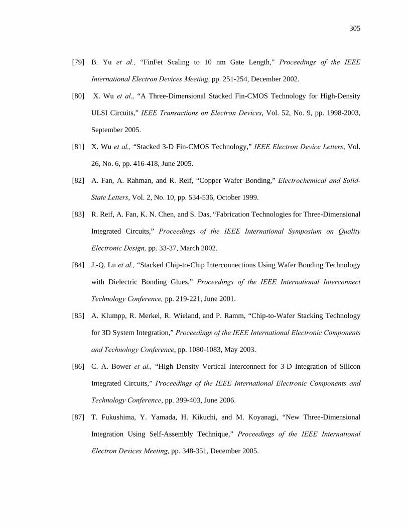
305
[79] B. Yu et al., “FinFet Scaling to 10 nm Gate Length,” Proceedings of the IEEE
International Electron Devices Meeting, pp. 251-254, December 2002.
[80] X. Wu et al., “A Three-Dimensional Stacked Fin-CMOS Technology for High-Density
ULSI Circuits,” IEEE Transactions on Electron Devices, Vol. 52, No. 9, pp. 1998-2003,
September 2005.
[81] X. Wu et al., “Stacked 3-D Fin-CMOS Technology,” IEEE Electron Device Letters, Vol.
26, No. 6, pp. 416-418, June 2005.
[82] A. Fan, A. Rahman, and R. Reif, “Copper Wafer Bonding,” Electrochemical and Solid-
State Letters, Vol. 2, No. 10, pp. 534-536, October 1999.
[83] R. Reif, A. Fan, K. N. Chen, and S. Das, “Fabrication Technologies for Three-Dimensional
Integrated Circuits,” Proceedings of the IEEE International Symposium on Quality
Electronic Design, pp. 33-37, March 2002.
[84] J.-Q. Lu et al., “Stacked Chip-to-Chip Interconnections Using Wafer Bonding Technology
with Dielectric Bonding Glues,” Proceedings of the IEEE International Interconnect
Technology Conference, pp. 219-221, June 2001.
[85] A. Klumpp, R. Merkel, R. Wieland, and P. Ramm, “Chip-to-Wafer Stacking Technology
for 3D System Integration,” Proceedings of the IEEE International Electronic Components
and Technology Conference, pp. 1080-1083, May 2003.
[86] C. A. Bower et al., “High Density Vertical Interconnect for 3-D Integration of Silicon
Integrated Circuits,” Proceedings of the IEEE International Electronic Components and
Technology Conference, pp. 399-403, June 2006.
[87] T. Fukushima, Y. Yamada, H. Kikuchi, and M. Koyanagi, “New Three-Dimensional
Integration Using Self-Assembly Technique,” Proceedings of the IEEE International
Electron Devices Meeting, pp. 348-351, December 2005.

306
[88] A. W. Topol et al., “Enabling SOI-Based Assembly Technology for Three-Dimensional
(3D) Integrated Circuits (ICs),” Proceedings of the IEEE International Electron Devices
Meeting, pp. 352-355, December 2005.
[89] S. Tiwari et al., “Three-Dimensional Integration for Silicon Electronics,” Proceedings of
the IEEE Lester Eastman Conference on High Performance Devices, pp. 24-33, August
2002.
[90] A. R. Mirza, “One Micron Precision, Wafer-Level Aligned Bonding for Interonnect,
MEMS and Packaging Applications,” Proceedings of the IEEE International Electronic
Components and Technology Conference, pp. 676-680, May 2000.
[91] N. Watanabe, T. Kojima, and T. Asano, “Wafer-Level Compliant Bump for Three-
Dimensional LSI with High-Density Area Bump Connections,” Proceedings of the IEEE
International Electron Devices Meeting, pp. 671-674, December 2005.
[92] R. N. Vrtis, K. A. Heap, W. F. Burgoyne, and L. M. Roberson, “Poly (Arylene Ethers) as
Low Dielectric Constant Materials for ULSI Interconnect Applications,” Proceedings of
the Materials Research Society Symposium, Vol. 443, p. 171, December 1997.
[93] N. H. Hendricks, “The Status of Low-k Materials Development,” Proceedings of the
International VLSI Multilevel Interconnect Conference, p. 17, June 2000.
[94] S. F. Hahn, S. J. Martin, and M. L. McKelvy, “Thermally Induced Polymerization of an
Arylvinylbenzocyclobenzene Monomer,” Macromolecules, Vol. 25, No. 5, pp. 1539-1545,
September 1992.
[95] D. Oben, P. Weigand, M. J. Shapiro, and S. A. Cohen, “Influence of the Cure Process on
the Properties of Hydrogen Silsequioxene Spin-on-Glass,” Proceedings of the Materials
Research Society Symposium, Vol. 443, p. 195, December 1997.

307
[96] T.-M. Lu and J. A. Moor, “Vapor Deposition of Low-Dielectric-Constant Polymeric Thin
Films,” Materials Research Bulletin, Vol. 22, No. 10, pp. 28-32, October 1997.
[97] S. A. Kühn, M. B. Kleiner, R. Thewes, and W. Weber, “Vertical Signal Transmission in
Three-Dimensional Integrated Circuits by Capacitive Coupling,” Proceedings of the IEEE
International Symposium on Circuits and Systems, Vol. 1, pp. 37-40, May 1995.
[98] A. Fazzi et al., “3-D Capacitive Interconnections for Wafer-Level and Die-Level
Assembly,” IEEE Journal of Solid State Circuits, Vol. 42, No. 10, pp. 2270-2282, October
2007.
[99] J. Xu et al., “AC Coupled Interconnect for Dense 3-D ICs,” IEEE Transactions on Nuclear
Science, Vol. 51, No. 5, pp. 2156-2160, October 2004.
[100] B. Kim et al., “Factors Affecting Copper Filling Process Within High Aspect Ratio Deep
Vias for 3D Chip Stacking,” Proceedings of the IEEE International Electronic
Components and Technology Conference, pp. 838-843, June 2006.
[101] M. W. Newman et al., “Fabrication and Electrical Characterization of 3D Vertical
Interconnects,” Proceedings of the IEEE International Electronic Components and
Technology Conference, pp. 394-398, June 2006.
[102] N. T. Nguyen et al., “Through-Wafer Copper Electroplating for Three-Dimensional
Interconnects,” Journal of Micromechanics and Microengineering, Vol. 12, No. 4, pp.
395-399, July 2002.
[103] C. S. Premachandran et al., “A Vertical Wafer Level Packaging Using Through Hole Filled
Via Interconnect by Lift-Off Polymer Method for MEMS and 3D Stacking Applications,”
Proceedings of the IEEE International Electronic Components and Technology
Conference, pp. 1094-1098, June 2005.

308
[104] F. Laermer, P. Schilp, and R. Bosch Gmbh, “Method of Anisotropically Etching Silicon,”
U.S. Patent 5,501,893, 1996; German Patent DE4241045C1, 1994.
[105] R. Nagarajan et al., “Development of a Novel Deep Silicon Tapered Via Etch Process for
Through-Silicon Interconnection in 3-D Integrated Systems,” Proceedings of the IEEE
International Electronic Components and Technology Conference, pp. 383-387, June 2006.
[106] P. Dixit and J. Miao, “Fabrication of High Aspect Ratio 35 µm Pitch Interconnects for
Next Generation 3-D Wafer Level Packaging by Through-Wafer Copper Electroplating,”
Proceedings of the IEEE International Electronic Components and Technology
Conference, pp. 388-393, June 2006.
[107] S. X. Zhang, S.-W. R. Lee, L. T. Weng, and S. So, “Characterization of Copper-to-Silicon
for the Application of 3D Packaging with Through Silicon Vias,” Proceedings of the IEEE
International Conference on Electronic Packaging Technology, pp. 51-56, September
2005.
[108] N. Ranganathan et al., “High Aspect Ratio Through-Wafer Interconnect for Three-
Dimensional Integrated Circuits,” Proceedings of the IEEE International Electronic
Components and Technology Conference, pp. 343-348, June 2005.
[109] D. Henry et al., “Low Electrical Resistance Silicon Through Vias: Technology and
Characterization,” Proceedings of the IEEE International Electronic Components and
Technology Conference, pp. 1360-1365, June 2006.
[110] C. Odoro et al., “Analysis of the Induced Stresses in Silicon During Thermocompression
Cu-Cu Bonding of Cu-Through-Vias in 3D-SIC Architecture,” Proceedings of the IEEE
International Electronic Components and Technology Conference, pp. 249-255, June 2007.

309
[111] D. Sabuncuoglu-Tezcan et al., “Sloped Through Wafer Vias for 3D Wafer Level
Packaging,” Proceedings of the IEEE International Electronic Components and
Technology Conference, pp. 643-647, June 2007.
[112] R. S. Patti, “Three-Dimensional Integrated Circuits and the Future of System-on-Chip
Designs,” Proceedings of the IEEE, Vol. 94, No. 6, pp. 1214-1224, June 2006.
[113] D. M. Jang et al., “Development and Evaluation of 3-D SiP with Vertically Interconnected
Through Silicon Vias (TSV),” Proceedings of the IEEE International Electronic
Components and Technology Conference, pp. 847-850, June 2007.
[114] B. S. Landman and R. L. Russo, “On a Pin Versus Block Relationship for Partitions of
Logic Graphs,” IEEE Transactions on Computers, Vol. C-20, No. 12, pp. 1469-1479,
December 1971.
[115] W. E. Donath, “Placement and Average Interconnection Lengths of Computer Logic,”
IEEE Transactions on Circuits and Systems, Vol. 26, No. 4, pp. 272-277, April 1979.
[116] P. Christie and D. Stroobandt, “The Interpretation and Application of Rent’s Rule,” IEEE
Transactions on Very Large Scale Integration (VLSI) Systems, Vol. 8, No. 6, pp. 639-648,
December 2000.
[117] P. Verplaetse, D. Stroobandt, and J. Van Campenhout, “A Stochastic Model for the
Interconnection Topology of Digital Circuits,” IEEE Transactions on Very Large Scale
Integration (VLSI) Systems, Vol. 9, No. 6, pp. 938-942, December 2001.
[118] A. B. Kahng, S. Mantik, and D. Stroobandt, “Toward Accurate Models of Achievable
Routing,” IEEE Transactions on Computer-Aided Design of Integrated Circuits and
Systems, Vol. 20, No. 5, pp. 648-659, May 2001.
[119] D. Stroobandt, A Priori Wire Length Estimates for Digital Design, Kluwer Academic
Publishers, Netherlands 2001.

310
[120] J. A. Davis, V. K. De, and J. D. Meindl, “A Stochastic Wire-Length Distribution for
Gigascale Integration (GSI) – Part I: Derivation and Validation,” IEEE Transactions on
Electron Devices, Vol. 45, No. 3, pp. 580-589, March 1998.
[121] J. A. Davis, V. K. De, and J. D. Meindl, “A Stochastic Wire-Length Distribution for
Gigascale Integration (GSI) – Part II: Applications to Clock Frequency, Power Dissipation,
and Chip Size Estimation,” IEEE Transactions on Electron Devices, Vol. 45, No. 3, pp.
590-597, March 1998.
[122] J. W. Joyner et al., “Impact of Three-Dimensional Architectures on Interconnects in
Gigascale Integration,” IEEE Transactions on Very Large Scale Integration (VLSI)
Systems, Vol. 9, No. 6, pp. 922-928, December 2001.
[123] J. W. Joyner, P. Zarkesh-Ha, J. A. Davis, and J. D. Meindl, “Vertical Pitch Limitations on
Performance Enhancement in Bonded Three-Dimensional Interconnect Architectures,”
Proceedings of the ACM International System Level Interconnect Prediction Conference,
pp. 123-127, April 2000.
[124] J. W. Joyner, P. Zarkesh-Ha, and J. D. Meindl, “A Stochastic Global Net-Length
Distribution for a Three-Dimensional System-on-a-Chip (3D-SoC),” Proceedings of the
IEEE International ASIC/SOC Conference, pp. 147-151, September 2001.
[125] J. W. Joyner, Opportunities and Limitations of Three-Dimensional Integration for
Interconnect Design, Ph.D. Dissertation, Georgia Institute of Technology, Atlanta,
Georgia, July 2003.
[126] A. Rahman, A. Fan, J. Chung, and R. Reif, “Wire-Length Distribution of Three-
Dimensional Integrated Circuits,” Proceedings of the IEEE International Interconnect
Technology Conference, pp. 233-235, May 1999.

311
[127] A. Rahman and R. Reif, “System Level Performance Evaluation of Three-Dimensional
Integrated Circuits,” IEEE Transactions on Very Large Scale Integration (VLSI) Systems,
Vol. 8, No. 6, pp. 671-678, December 2000.
[128] A. Rahman, A. Fan, and R. Reif, “Comparison of Key Performance Metrics in Two- and
Three-Dimensional Integrated Circuits,” Proceedings of the IEEE International
Interconnect Technology Conference, pp. 18-20, June 2000.
[129] R. Zhang, K. Roy, C.-K. Koh, and D. B. Janes, “Stochastic Interconnect Modeling, Power
Trends, and Performance Characterization of 3-D Circuits,” IEEE Transactions on
Electron Devices, Vol. 48, No. 4, pp. 638-652, April 2001.
[130] R. Zhang, K. Roy, C.-K. Koh, and D. B. Janes, “Power Trends and Performance
Characterization of 3-Dimensional Integration,” Proceedings of the IEEE International
Symposium on Circuits and Systems, Vol. IV, pp. 414-417, May 2001.
[131] D. Stroobandt and J. Van Campenhout, “Accurate Interconnection Lengths in Three-
Dimensional Computer Systems,” IEICE Transactions on Information and System, Special
Issue on Physical Design in Deep Submicron, Vol. 10, No. 1, pp. 99-105, April 2000.
[132] D. Stroobandt, H. Van Marck, and J. Van Campenhout, “On the Use of Generating
Polynomials for the Representation of Interconnection Length Distributions,” Proceedings
of the International Workshop on Symbolic Methods and Applications to Circuit Design,
pp. 74-78, October 1996.
[133] D. Stroobandt, “Improving Donath’s Technique for Estimating the Average
Interconnection Length in Computer Logic,” Technical Report DG 96-01, Ghent
University, Belgium, ELIS Department, June 1996.
[134] W. E. Donath, “Wire Length Distribution for Placements of Computer Logic,” IBM
Journal of Research and Development, Vol. 25, No. 2/3, pp. 152-155, May 1981.

312
[135] K. C. Saraswat, S. K. Souri, K. Banerjee, and P. Kapour, “Performance Analysis and
Technology of 3-D ICs,” Proceedings of the ACM International System Level Interconnect
Prediction Conference, pp. 85-90, April 2000.
[136] K. Banerjee, S. K. Souri, P. Kapour, and K. C. Saraswat, “3-D ICs: A Novel Chip Design
Paradigm for Improving Deep-Submicrometer Interconnect Performance and Systems-on-
Chip Integration,” Proceedings of the IEEE, Vol. 89, No. 5, pp. 602-633, May 2001.
[137] J. W. Joyner, P. Zarkesh-Ha, and J. D. Meindl, “A Global Interconnect Design Window for
a Three-Dimensional System-on-a-Chip,” Proceedings of the IEEE International
Interconnect Technology Conference, pp. 154-156, June 2001.
[138] J. W. Joyner and J. D. Meindl, “Opportunities for Reduced Power Distribution Using
Three-Dimensional Integration,” Proceedings of the IEEE International Interconnect
Technology Conference, pp. 148-150, June 2002.
[139] “FDSOI Design Guide,” MIT Lincoln Lab., Cambridge, 2006.
[140] H. Hua et al., “Performance Trend in Three-Dimensional Integrated Circuits,” Proceedings
of the IEEE International Interconnect Technology Conference, pp. 45-47, June 2006.
[141] OpenRISC Reference Platform System-on-a-Chip and OpenRISC I200 IP Core
Specification, online [http://www.opencores.org/projects.cgi/web/orlk/orpso].
[142] K. Bernstein et al., “Interconnects in the Third Dimension: Design Challenges for 3-D
ICs,” Proceedings of the IEEE/ACM Design Automation Conference, pp. 562-567, June
2007.
[143] S. A. Kühn, M. B. Kleiner, P. Ramm, and W. Weber, “Performance Modeling of the
Interconnect Structure of a Three-Dimensional Integrated RISC Processor/Cache System,”
IEEE Transactions on Components, Packaging, and Manufacturing Technology – Part B,
Vol. 19, No. 4, pp. 719-727, November 1996.

313
[144] R. H. J. M. Otten, “Automatic Floorplan Design,” Proceedings of the IEEE/ACM Design
Automation Conference, pp. 261-267, June 1982.
[145] X. Hong et al., “Corner Block List: An Effective and Efficient Topological Representation
of Non-Slicing Floorplan,” Proceedings of the IEEE/ACM International Conference on
Computer-Aided Design, pp. 8-11, November 2000.
[146] E. F. Y. Yong, C. C. N. Chu, and C. S. Zion, “Twin Binary Sequences: A Non-Redundant
Representation for General Non-Slicing Floorplan,” IEEE Transactions on Computer-
Aided Design of Integrated Circuits and Systems, Vol. 22, No. 4, pp. 457-469, April 2003.
[147] J. M. Lin and Y. W. Chang, “TCG: A Transitive Closure Graph Based Representation for
Non-Slicing Floorplans,” Proceedings of the IEEE/ACM Design Automation Conference,
pp. 764-769, June 2001.
[148] H. Yamazaki, K. Sakanushi, S. Nakatake, and Y. Kajitani, “The 3D-Packing by Meta Data
Structure and Packing Heuristics,” IEICE Transactions on Fundamentals of Electronics,
Communications and Computer Sciences, Vol. E83-A, No. 4, pp. 639-645, April 2000.
[149] L. Cheng, L. Deng, and D. F. Wong, “Floorplanning for 3-D VLSI Design,” Proceedings
of the IEEE Asia and South Pacific Design Automation Conference, pp. 405-411, January
2005.
[150] Z. Li et al., “Hierarchical 3-D Floorplanning Algorithm for Wirelength Optimization,”
IEEE Transactions on Circuits and Systems I: Regular Papers, Vol. 53, No. 12, pp. 2637-
2646, December 2006.
[151] Y. Deng and W. P. Maly, “Interconnect Characteristics of 2.5-D System Integration
Scheme,” Proceedings of the IEEE International Symposium on Physical Design, pp. 341-
345, April 2001.

314
[152] S. Salewski and E. Barke, “An Upper Bound for 3D Slicing Floorplans,” Proceedings of
the IEEE Asia and South Pacific Design Automation Conference, pp. 567-572, January
2002.
[153] P. H. Shiu, R. Ravichandran, S. Easwar, and S. K. Lim, “Multi-Layer Floorplanning for
Reliable System-on-Package,” Proceedings of the IEEE International Symposium on
Circuits and Systems, Vol. V, pp. 69-72, May 2004.
[154] J. Cong, J. Wei, and Y. Zhang, “A Thermal-Driven Floorplanning Algorithm for 3-D ICs,”
Proceedings of the IEEE/ACM International Conference on Computer-Aided Design, pp.
306-313, November 2004.
[155] T. Yan, Q. Dong, Y. Takashima, and Y. Kajitani, “How Does Partitioning Matter for 3D
Floorplanning,” Proceedings of the ACM International Great Lakes Symposium on VLSI,
pp. 73-76, April/May 2006.
[156] [Online]. Available: http://www.cse.ucsc.edu/research/surf/GSRC/progress.html
[157] X. Hong et al., “Non-Slicing Floorplan and Placement Using Corner Block List
Topological Representation,” IEEE Transactions on Circuits and Systems II: Express
Briefs, Vol. 51, No. 5, pp. 228-233, May 2004.
[158] M. Healy et al., “Multiobjective Microarchitectural Floorplanning for 2-D and 3-D ICs,”
IEEE Transactions on Computer-Aided Design of Integrated Circuits and Systems, Vol.
26, No. 1, pp. 38-52, January 2007.
[159] P. Shivakumar and N. P. Jouppi, “CACTI 3.0: An Integrated Cache Timing, Power, and
Area Model,” HP Western Research Labs, Palo Alto, CA, Technical Report 2001.2, 2001.
[160] J. C. Eble, V. K. De, D. S. Wills, and J. D. Meindl, “A Generic System Simulator
(GENESYS) for ASIC Technology and Architecture Beyond 2001,” Proceedings of the
IEEE International ASIC Conference, pp. 193-196, September 1996.

315
[161] T. M. Austin, Simplescalar Tool Suite. [Online]. Available: http://www.simplescalar.com
[162] D. Brooks, V. Tiwari, and M. Martonosi, “Wattch: A Framework for Architectural-Level
Power Analysis and Optimizations,” Proceedings of the IEEE International Conference on
Computer Architecture, pp. 83-94, June 2000.
[163] N. A. Sherwani, Algorithms for VLSI Physical Design Automation, Kluwer Academic
Publishers, 3rd edition, 2002.
[164] M. Ohmura, “An Initial Placement Algorithm for 3-D VLSI,” Proceedings of the IEEE
International Symposium on Circuits and Systems, Vol. IV, pp. 195-198, May 1998.
[165] T. Tanprasert, “An Analytical 3-D Placement that Preserves Routing Space,” Proceedings
of the IEEE International Symposium on Circuits and Systems, Vol. III, pp. 69-72, May
2000.
[166] I. Kaya, M. Olbrich, and E. Barke, “3-D Placement Considering Vertical Interconnects,”
Proceedings of the IEEE International SOC Conference, pp. 257-258, September 2003.
[167] R. Hentschke and R. Reis, “A 3D-Via Legalization Algorithm for 3D VLSI Circuits and its
Impact on Wire Length,” Proceedings of the IEEE International Symposium on Circuits
and Systems, pp. 2036-2039, May 2007.
[168] R. Hentschke, G. Flach, F. Pinto, and R. Reis, “Quadratic Placement for 3D Circuits Using
Z-Cell Shifting, 3D Iterative Refinement and Simulated Annealing,” Proceedings of the
ACM International Symposium on Integrated Circuits and System Design, pp. 220-225,
September 2006.
[169] E. Wong, J. Minz, and S. K. Lim, “Multi-Objective Module Placement for 3-D System-
On-Package,” IEEE Transactions on Very Large Scale Integration (VLSI) Systems, Vol.
14, No. 5, pp. 553-557, May 2006.

316
[170] H. Murata, K. Fujiyoshi, S. Nakatake, and Y. Kajitani, “Rectangle Packing Based Module
Placement,” Proceedings of the IEEE International Conference on Computer-Aided
Design, pp. 472-479, November 1995.
[171] E. Wong, J. Minz, and S. K. Lim, “Power Supply Noise-Aware 3D Floorplanning for
System-on-Package,” Proceedings of the IEEE Topical Meeting on Electrical Performance
on Electronic Packaging, pp. 259-262, October 2005.
[172] M. Popovich and E. G. Friedman, “Decoupling Capacitors for Multi-Voltage Power
Distribution Systems,” IEEE Transactions on Very Large Scale Integration (VLSI)
Systems, Vol. 14, No. 3, pp. 217-228, March 2006.
[173] A. Mezhiba and E. G. Friedman, Power Distribution Networks in High Speed Integrated
Circuits, Kluwer Academic Publishers, 2004.
[174] M. Popovich, A. V. Mezhiba, and E. G. Friedman, Power Distribution Networks with On-
Chip Decoupling Capacitors, Springer Verlag, 2008.
[175] J. Minz, S. K. Lim, and C.-K. Koh, “3D Module Placement for Congestion and Power
Noise Reduction,” Proceedings of the ACM International Great Lakes Symposium on
VLSI, pp. 458-461, April 2005.
[176] [Online]. Available: http://www.gtcad.gatech.edu
[177] R. J. Enbody, G. Lynn, and K. H. Tan, “Routing the 3-D Chip,” Proceedings of the
IEEE/ACM Design Automation Conference, pp. 132-137, June 1991.
[178] S. Tayu and S. Ueno, “On the Complexity of Three-Dimensional Channel Routing,”
Proceedings of the IEEE International Symposium on Circuits and Systems, pp. 3399-
3402, May 2007.
[179] C. C. Tong and C.-L. Wu, “Routing in a Three-Dimensional Chip,” IEEE Transactions on
Computers, Vol. 44, No. 1, pp. 106-117, January 1995.

317
[180] A. Hashimoto and J. Stevens, “Wire Routing by Optimizing Channel Assignment within
Large Apertures,” Proceedings of the IEEE/ACM Design Automation Conference, pp. 155-
169, June 1971.
[181] T. Ohtsuki, Advances in CAD for VLSI: Vol. 4, Layout Design and Verification, Elsevier,
1986.
[182] J. Minz and S. K. Lim, “Block-Level 3-D Global Routing With an Application to 3-D
Packaging,” IEEE Transactions on Computer-Aided Design of Integrated Circuits and
Systems, Vol. 25, No. 10, pp. 2248-2257, October 2006.
[183] A. Harter, Three-Dimensional Integrated Circuit Layout, Cambridge University Press,
1991.
[184] B. Hoefflinger, S. T. Liu, and B. Vajdic, “A Three-Dimensional CMOS Design
Methodology,” IEEE Transactions on Electron Devices, Vol. ED-31, No. 2, pp. 171-173,
February 1984.
[185] S. M. Alam, D. E. Troxel, and C. V. Thompson, “A Comprehesive Layout Methodology
and Layout-Specific Circuit Analyses for Three-Dimensional Integrated Circuits,”
Proceedings of the IEEE International Symposium on Quality Electronic Design, pp. 246-
251, March 2002.
[186] S. Das, A. Chandrakasan, and R. Reif, “Design Tools for 3-D Integrated Circuits,”
Proceedings of the IEEE Asia and South Pacific Design Automation Conference, pp. 53-
56, January 2003.
[187] [Online]. Available: http://www.ece.ncsu.edu/erl/3DIC/pub
[188] [Online]. Available: http://www.xilinx.com
318
[189] M. J. Alexander et al., “Placement and Routing for Three-Dimensional FPGAs,”
Proceedings of the Canadian Workshop on Field-Programmable Devices, pp. 11-18, May
1996.
[190] [Online]. Available: http://www.xilinx.com/products/silicon_solutions/fpgas/
spartan_series /spartan3_fpgas/index.htm
[191] A. Rahman, S. Das, A. P. Chandrakasan, and R. Reif, “Wiring Requirement and Three-
Dimensional Integration Technology for Field Programmable Gate Arrays,” IEEE
Transactions on Very Large Scale Integration (VLSI) Systems, Vol. 11, No. 1, pp. 44-53,
February 2003.
[192] G. G. Lemieux and S. D. Brown, “A Detailed Routing Algorithm for Allocating Wire
Segments in Field-Programmable Gate Arrays,” Proceedings of the IEEE Physical Design
Workshop, pp. 215-226, April 1993.
[193] V. Betz and J. Rose, “VPR: A New Packing, Placement, and Routing Tool for FPGA
Research,” Proceedings of the International Workshop on Field Programmable Logic
Applications, pp. 213-222, September 1997.
[194] M. J. Alexander et al., “Three-Dimensional Field-Programmable Gate Arrays,”
Proceedings of the IEEE International ASIC Conference, pp. 253-256, September 1995.
[195] M. J. Alexander, J. P. Cohoon, J. L. Ganley, and G. Robins, “Performance-Oriented
Placement and Routing for Field-Programmable Gate Arrays,” Proceedings of the IEEE
International European Design Automation Conference, pp. 80-85, September 1995.
[196] M. J. Alexander, J. P. Cohoon, J. L. Ganley, and G. Robins, “An Architecture-Independent
Approach to FPGA Routing Based on Multi-Weighted Graphs,” Proceedings of the IEEE
International European Design Automation Conference, pp. 259-264, September 1995.

319
[197] C. Ababei, H. Mogal, and K. Bazargan, “Three-Dimensional Place and Route for FPGAs,”
Proceedings of the IEEE Asia and South Pacific Design Automation Conference, pp. 773-
778, January 2005.
[198] V. Betz, J. Rose, and A. Marquardt, Architecture and CAD for Deep-Submicron FPGAs,
Kluwer Academic Publishers, 1999.
[199] G. Karypis, R. Aggarwal, V. Kumar, and S. Shekhar, “Multilevel Hypergraph Partitioning:
Applications in VLSI Domain,” IEEE Transactions on Very Large Scale Integration
(VLSI) Systems, Vol. 7, No.1, pp. 69-79, March 1999.
[200] P. Maidee, C. Ababei, and K. Bazargan, “Fast Timing-Driven Partitioning Based
Placement for Island Style FPGAs,” Proceedings of the ACM/IEEE International
Conference on Design Automation, pp. 598-603, June 2003.
[201] C. Ebeling, L. McMurchie, S. A. Hauck, and S. Burns, “Placement and Routing Tools for
the Triptych FPGAs,” IEEE Transactions on Very Large Scale Integration (VLSI) Systems,
Vol. 3, No. 4, pp. 472-483, December 1995.
[202] M. Lin, A. El Gamal, Y.-C. Lu, and S. Wong, “Performance Benefits of Monolithically
Stacked 3-D FPGA,” IEEE Transactions on Computer-Aided Design of Integrated Circuits
and Systems, Vol. 26, No. 2, pp. 216-229, February 2007.
[203] K. Banerjee, A. Mehrotra, A. Sangiovanni-Vincentelli, and C. Hu, “On Thermal Effects in
Deep Sub-Micron VLSI Interconnects,” Proceedings of the IEEE/ACM Design Automation
Conference, pp. 885-890, June 1999.
[204] C. H. Tsai and S.-M. Kang, “Cell-Level Placement for Improving Substrate Thermal
Distribution,” Vol. 19, No. 2, pp. 253-266, February 2000.
[205] V. Szekely, M. Rencz, and B. Courtois, “Tracing the Thermal Behavior of ICs,” IEEE
Design and Test of Computers, Vol. 15, No. 2, pp. 14-21, April/June 1998.

320
[206] M. B. Kleiner, S. A. Kühn, P. Ramn, and W. Weber, “Thermal Analysis of Vertically
Integrated Circuits,” Proceedings of the IEEE International Electron Devices Meeting, pp.
487-490, December 1995.
[207] S. Im and K. Banerjee, “Full Chip Thermal Analysis of Planar (2-D) and Vertically
Integrated (3-D) High Performance ICs,” Proceedings of the IEEE International Electron
Devices Meeting, pp. 727-730, December 2000.
[208] T.-Y. Chiang, S. J. Souri, C. O. Chui, and K. C. Saraswat, “Thermal Analysis of
Heterogeneous 3-D ICs with Various Integration Scenarios,” Proceedings of the IEEE
International Electron Devices Meeting, pp. 681-684, December 2001.
[209] C. C. Liu, J. Zhang, A. K. Datta, and S. Tiwari, “Heating Effects of Clock Drivers in Bulk,
SOI, and 3-D CMOS,” IEEE Transactions on Electron Device Letters, Vol. 23, No. 12, pp.
716-728, December 2002.
[210] Z. Tan, M. Furmanczyk, M. Turowski, and A. Przekwas, “CFD-Micromesh: A Fast
Geometrical Modeling and Mesh Generation Tool for 3D Microsystem Simulations,”
Proceedings of the International Conference on Modeling and Simulation of Microsystems,
pp. 712-715, March 2000.
[211] P. Wilkerson, M. Furmanczyk, and M. Turowski, “Compact Thermal Model Analysis for
3-D Integrated Circuits,” Proceedings of the International Conference on Mixed Design of
Integrated Circuits and Systems, pp. 277-282, June 2004.
[212] P. Wilkerson, M. Furmanczyk, and M. Turowski, “Fast, Automated Thermal Simulation of
Three-Dimensional Integrated Circuits,” Proceedings of the Intersociety Conference on
Thermal and Thermomechanical Phenomena in Electronic Systems, pp. 706-713, June
2004.

321
[213] M. N. Sabry and H. Saleh, “Compact Thermal Models: A Global Approach,” Proceedings
of the IEEE International Conference on Thermal Issues in Emerging Technologies, pp.
33-39, January 2007.
[214] G. Digele, S. Lindenkreuz, and E. Kasper, “Fully Coupled Dynamic Electro-Thermal
Simulation,” IEEE Transactions on Very Large Scale Integration (VLSI) Systems, Vol. 5,
No. 3, pp. 250–257, September 1997.
[215] S. Wunsche, C. Claub, and P. Schwarz, “Electro-Thermal Circuit Simulation Using
Simulator Coupling,” IEEE Transactions on Very Large Scale Integration (VLSI) Systems,
Vol. 5, No. 3, pp. 277–282, September 1997.
[216] K. Puttaswamy and G. H. Loh, “Thermal Analysis of a 3-D Die Stacking High-
Performance Microprocessor,” Proceedings of the ACM International Great Lakes
Symposium on VLSI, pp. 19-24, April/May 2006.
[217] J. Cong, J. Wei, and Y. Zhang, “A Thermal-Driven Floorplanning Algorithm for 3-D ICs,”
Proceedings of the IEEE/ACM International Conference on Computer-Aided Design, pp.
306-310, November 2004.
[218] W.-L. Hung et al., “Interconnect and Thermal-Aware Floorplanning for 3-D
Microprocessors,” Proceedings of the IEEE International Symposium on Quality
Electronic Design, pp. 98-103, March 2006.
[219] [Online]. Available: http://www.crhc.uiuc.edu/ACS/tools/ivm/about.html
[220] C. Addo-Quaye, “Thermal-Aware Mapping and Placement for 3-D NoC Designs,”
Proceedings of the IEEE International SOC Conference, pp. 25-28, September 2005.
[221] D. E. Goldberg, Genetic Algorithms in Search, Optimization, and Machine Learning,
Addison-Wesley, 1989.

322
[222] H. Eisenmann and F. M. Johannnes, “Generic Global Placement and Floorplanning,”
Proceedings of the IEEE/ACM Design Automation Conference, pp. 269-274, June 1998.
[223] B. Goplen and S. Sapatnekar, “Efficient Thermal Placement of Standard Cells in 3-D ICs
using a Force Directed Approach,” Proceedings of the IEEE/ACM International
Conference on Computer-Aided Design, pp. 86-89, November 2003.
[224] M. E. Van Valkenburg, Network Analysis, 3rd edition, Prentice-Hall, 1974.
[225] [Online]. Available: http://er.cs.ucla.edu/benchmarks/ibm-place
[226] [Online]. Available: http://www.cbl.ncsu.edu/pub/Benchmark_dirs/LayoutSynth92
[227] B. Goplen and S. Sapatnekar “Placement of Thermal Vias in 3-D ICs Using Various
Thermal Objectives,” IEEE Transactions on Computer-Aided Design of Integrated
Circuits and Systems, Vol. 25, No. 4, pp. 692-709, April 2006.
[228] J. Cong and Y. Zhang, “Thermal Driven Multilevel Routing for 3-D ICs,” Proceedings of
the IEEE Asia and South Pacific Design Automation Conference, pp. 121-126, June 2005.
[229] J. Cong and Y. Zhang, “Thermal Via Planning for 3-D ICs,” Proceedings of the
IEEE/ACM International Conference on Computer-Aided Design, pp. 744-751, November
2005.
[230] J. Cong, M. Xie, and Y. Zhang, “An Enhanced Multilevel Routing System,” Proceedings
of the IEEE/ACM International Conference on Computer-Aided Design, pp. 51-58,
November 2002.
[231] J. Cong, J. Fang, and Y. Zhang, “Multilevel Approach to Full-Chip Gridless Routing,”
Proceedings of the IEEE/ACM International Conference on Computer-Aided Design, pp.
234-241, November 2001.

323
[232] Z. Li et al., “Efficient Thermal Via Planning Approach and its Application in 3-D
Floorplanning,” IEEE Transactions on Computer-Aided Design of Integrated Circuits and
Systems, Vol. 26, No. 4, pp. 645-658, April 2007.
[233] T. H. Cormen, C. E. Leiserson, and R. L. Rivest, Introduction to Algorithms, The MIT
Press, 1990.
[234] T. Zhang, Y. Zhang, and S. Sapatnekar, “Temperature-Aware Routing in 3-D ICs,”
Proceedings of the IEEE Asia and South Pacific Design Automation Conference, pp. 309-
314, January 2006.
[235] J. A. Burns et al., “A Wafer-Scale 3-D Circuit Integration Technology,” IEEE
Transactions on Electron Devices, Vol. 53, No. 10, pp. 2507-2515, October 2006.
[236] G. Chen and E. G. Friedman, “An RLC Interconnect Model Based on Fourier Analysis,”
IEEE Transactions on Computer-Aided Design of Integrated Circuits and Systems, Vol.
24, No. 2, pp. 170-183, February 2005.
[237] C. Ryu et al., “High Frequency Electrical Circuit Model of Chip-to-Chip Vertical Via
Interconnection for 3-D Chip Stacking Package,” Proceedings of the IEEE Topical
Meeting on Electrical Performance of Electronic Packaging, pp 151-154, October 2005.
[238] Metal User’s Guide, www.oea.com
[239] P. Ramn et al., “InterChip Via Technology for Vertical System Integration,” Proceedings
of the IEEE International Interconnect Technology Conference, pp. 160-162, June 2001.
[240] K. D. Boese et al., “Fidelity and Near-Optimality of Elmore-Based Routing
Constructions,” Proceedings of the IEEE International Conference on Computer Design,
pp. 81-84, October 1993.

324
[241] A. I. Abou-Seido, B. Nowak, and C. Chu, “Fitted Elmore Delay: A Simple and Accurate
Interconnect Delay Model,” IEEE Transactions on Very Large Scale Integration (VLSI)
Systems, Vol. 12, No. 7, pp. 691-696, July 2004.
[242] J. P. Fishburn and C. A. Schevon, “Shaping a Distributed-RC Line to Minimize Elmore
Delay,” IEEE Transactions on Circuits and Systems I: Fundamental Theory and
Applications, Vol. 42, No. 12, pp. 1020-1022, December 1995.
[243] J. Cong and K.-S. Leung, “Optimal Wiresizing under Elmore Delay Model,” IEEE
Transactions on Computer-Aided Design of Integrated Circuits and Systems, Vol. 14, No.
3, pp. 321–336, March 1995.
[244] J. D. Cho et al., “Crosstalk-Minimum Layer Assignment,” Proceedings of the IEEE
Conference on Custom Integrated Circuits, pp. 29.7.1 – 29.7.4, May 1993.
[245] J. G. Ecker, “Geometric Programming: Methods, Computations and Applications,” SIAM
Review, Vol. 22, No. 3, pp. 338-362, July 1980.
[246] S. Boyd, S. J. Kim, L. Vandenberghe, and A. Hassibi, “A Tutorial on Geometric
Programming,” Optimization and Engineering, Vol. 8, No. 1, pp. 67-127, March 2007.
[247] Predictive Technology Model [Online]. Available: http://www.eas.asu.edu/~ptm
[248] W. Zhao and Y. Cao, “New Generation of Predictive Technology Model for Sub-45nm
Design Exploration,” Proceedings of the IEEE International Symposium on Quality
Electronic Design, pp. 585-590, March 2006.
[249] J. Löfberg, “YALMIP: A Toolbox for Modeling and Optimization in MATLAB,”
Proceedings of the IEEE International Symposium on Computer-Aided Control Systems
Design, pp. 284-289, September 2004.

325
[250] D. Henrion and J. B. Lasserre, “GloptiPoly: Global Optimization over Polynomials with
Matlab and SeDuMi,” ACM Transactions on Mathematical Software, Vol. 29, No. 2, pp.
165-194, June 2003.
[251] C.-P. Che, H. Zhou, and D. F. Wong, “Optimal Non-Uniform Wire-Sizing under the
Elmore Delay Model,” Proceedings of the IEEE/ACM International Conference on
Computer-Aided Design, pp. 38-43, November 1996.
[252] D. Bertozzi et al., “NoC Synthesis Flow for Customized Domain Specific Multiprocessor
Systems-on-Chip,” IEEE Transactions on Parallel and Distributed Systems, Vol. 16, No.
2, pp. 113-129, February 2005.
[253] J. C. Koob et al., “Design of a 3-D Fully Depleted SOI Computational RAM,” IEEE
Transactions on Very Large Scale Integration (VLSI) Systems, Vol. 13, No. 3, pp. 358-368,
March 2005.
[254] S. Kumar et al., “A Network on Chip Architecture and Design Methodology,” Proceedings
of the International IEEE Annual Symposium on VLSI, pp. 105-112, April 2002.
[255] V. F. Pavlidis and E. G. Friedman, “3-D Topologies for Networks-on-Chip,” Proceedings
of the IEEE International SOC Conference, pp. 285-288, September 2006.
[256] V. F. Pavlidis and E. G. Friedman, “3-D Topologies for Networks-on-Chip,” IEEE
Transactions on Very Large Scale Integration (VLSI) Systems, Vol. 15, No. 10, pp. 1081-
1090, October 2007.
[257] F. Li et al., “Design and Management of 3D Chip Multiprocessors Using Network-in-
Memory,” Proceedings of the IEEE International Symposium on Computer Architecture,
pp. 130-142, June 2006.
[258] W. J. Dally, “Performance Analysis of k-ary n-cube Interconnection Networks,” IEEE
Transaction on Computers, Vol. 39, No. 6, pp. 775-785, June 1990.

326
[259] A. Jantsch and H. Tenhunen, Networks on Chip, Kluwer Academic Publishers, 2003.
[260] M. Millberg et al., “The Nostrum Backbone - A Communication Protocol Stack for
Networks on Chip,” Proceedings of the IEEE International Conference on VLSI Design,
pp. 693-696, January 2004.
[261] J. M. Duato, S. Yalamanchili, and L. Ni, Interconnection Networks: An Engineering
Approach, Morgan Kaufmann, 2003.
[262] W. J. Dally and B. Towles, Principles and Practices of Interconnection Networks, Morgan
Kaufmann, 2004.
[263] L.-S. Peh and W. J. Dally, “A Delay Model for Router Microarchitectures,” IEEE Micro,
Vol. 21, No. 1, pp. 26-34, January/February 2001.
[264] T. Sakurai, “Closed-Form Expressions for Interconnection Delay, Coupling, and Crosstalk
in VLSIs,” IEEE Transactions on Electron Devices, Vol. 40, No. 1, pp. 118-124, January
1993.
[265] T. Sakurai and A. R. Newton, “Alpha-Power Law MOSFET Model and its Applications to
CMOS Inverter Delay and other Formulas,” IEEE Journal of Solid State Circuits, Vol. 25,
No. 2, pp. 584-594, April 1990.
[266] G. Chen and E. G. Friedman, “Low-Power Repeaters Driving RC and RLC Interconnects
With Delay and Bandwidth Constraints,” IEEE Transactions on Very Large Integration
(VLSI) Systems, Vol. 12, No. 2, pp. 161-172, February 2006.
[267] Y. I. Ismail, E. G. Friedman, and J. L. Neves, “Equivalent Elmore Delay for RLC trees,”
IEEE Transactions on Computer-Aided Design of Integrated Circuits and Systems, Vol.
19, No. 1, pp. 83-97, January 2000.

327
[268] Y. I. Ismail, E. G. Friedman, and J. L. Neves, “Figures of Merit to Characterize the
Importance of On-Chip Inductance,” IEEE Transactions on Very Large Scale Integration
(VLSI) Systems, Vol. 7, No. 4, pp. 442-449, December 1999.
[269] K. Banerjee and A. Mehrotra, “A Power-Optimal Repeater Insertion Methodology for
Global Interconnects in Nanometer Design,” IEEE Transactions on Electron Devices, Vol.
49, No. 11, pp. 2001-2007, November 2002.
[270] H. J. M. Veendrick, “Short-Circuit Dissipation of Static CMOS Circuitry and its Impact on
the Design of Buffer Circuits,” IEEE Journal of Solid State Circuits, Vol. SC-19, No. 4,
pp. 468-473, August 1984.
[271] K. Nose and T. Sakurai, “Analysis and Future Trend of Short-Circuit Power,” IEEE
Transactions on Computer-Aided Design of Integrated Circuits and Systems, Vol. 19, No.
9, pp. 1023-1030, September 2000.
[272] G. Chen and E. G. Friedman, “Effective Capacitance of RLC Loads for Estimating Short-
Circuit Power,” Proceedings of the IEEE International Symposium on Circuits and
Systems, pp. 2065-2068, May 2006.
[273] P. R. O’Brien and T. L. Savarino, “Modeling the Driving-Point Characteristic of Resistive
Interconnect for Accurate Delay Estimation,” Proceedings of the IEEE/ACM International
Conference on Computer-Aided Design, pp. 512-515, April 1989.
[274] H. Wang, L.-S. Peh, and S. Malik, “Power-Driven Design of Router Microarchitectures in
On-Chip Networks,” Proceedings of the IEEE International Symposium on
Microarchitecture, pp. 105-116, December 2003.
[275] C. Marcon et al., “Exploring NoC Mapping Strategies: an Energy and Timing Aware
Technique,” Proceedings of the ACM/IEEE Design, Automation and Test in Europe
Conference and Exhibition, Vol. 1, pp. 502-507, March 2005.
328
[276] P. P. Pande et al., “Performance Evaluation and Design Trade-Offs for Network-on-Chip
Interconnect Architectures,” IEEE Transactions on Computers, Vol. 54, No. 8, pp. 1025-
1039, August 2005.
[277] E. G. Friedman (Ed.), Clock Distribution Networks in VLSI Circuits and Systems, New
Jersey, IEEE Press, 1995.
[278] D. W. Bailey and B. J. Benschneider, “Clocking Design and Analysis for a 600-MHz
Alpha Microprocessor,” IEEE Journal of Solid-State Circuits, Vol. 22, No. 11, pp. 1627-
1633, November 1998.
[279] T. Xanthopoulos et al., “The Design and Analysis of the Clock Distribution Network for a
1.2 GHz Alpha Microprocessor,” Proceedings of the IEEE International Solid-State
Circuits Conference, pp. 402-402, February 2001.
[280] H. B. Bakoglu, Circuits, Interconnections, and Packaging for VLSI, Addison-Wesley,
1990.
[281] V. Pavlidis and E. G. Friedman, “Interconnect Delay Minimization through Interlayer Via
Placement in 3-D ICs,” Proceedings of the ACM Great Lakes Symposium on VLSI, pp. 20-
25, April 2005.
[282] W. Cui, H. Chen, and Y. Han, “VLSI Implementation of Universal Random Number
Generator,” Proceedings of the IEEE Asia-Pacific Conference on Circuits and Systems,
Vol. 1, pp. 465-470, October 2002.
[283] A. Deutsch and P. J. Restle, “Designing the Best Clock Distribution Network,”
Proceedings of the IEEE Symposium on VLSI Circuits, pp. 2-5, June 1998.
[284] E. G. Friedman, “Clock Distribution Networks in Synchronous Digital Integrated
Circuits,” Proceedings of the IEEE, Vol. 89, No. 5, pp. 665-692, May 2001.

329
[285] N. Hedenstierna and K. O. Jeppson, “CMOS Circuit Speed and Buffer Optimization,”
IEEE Transactions on Computer-Aided Design, Vol. CAD-6, No. 2, pp. 270-281, March
1987.
[286] N. C. Li, G. L. Haviland, and A. A. Tuszynski, “CMOS Tapered Buffer,” IEEE Journal of
Solid-State Circuits, Vol. 25, No. 4, pp. 1005-1008, August 1990.
[287] C. Punty and L. Gal, “Optimum Tapered Buffer,” IEEE Journal of Solid-State Circuits,
Vol. 27, No. 1, pp. 1005-1008, January 1992.
[288] A. Dharchoudhury, R. Panda, D. Blaauw, and R. Vaidyanathan, “Design and Analysis of
Power Distribution Networks in PowerPC Microprocessors,” Proceedings of the
IEEE/ACM International Conference on Design Automation, pp 738-743, June 1998.
[289] A. V. Mezhiba and E. G. Friedman, “Inductive Properties of High-Performance Power
Distribution Grids,” IEEE Transactions on Very Large Scale Integration (VLSI) Systems,
Vol. 10, No. 6, pp. 762-776, December 2002.
[290] A. V. Mezhiba and E. G. Friedman, “Impedance Characteristics of Power Distribution
Grids in Nanoscale Integrated Circuits,” IEEE Transactions on Very Large Scale
Integration (VLSI) Systems, Vol. 12, No. 11, pp. 1148-1155, November 2004.
[291] A. Bartzas, N. Skalis, and D. Soudris “Exploration of Alternative Topologies for
Application-Specific 3D Networks-on-Chip,” Proceedings of the International Workshop
on Application Specific Processors, pp. 55-62, October 2007.

330
Appendix A: Enumeration of Gate Pairs in a 3-D
IC The starting gates Nstart used in the derivation of the interconnect length distribution for 3-D
circuits in [122] are described, in this appendix. Starting gates are these gates that can form
manhattan hemispheres of radius l, where l is the interconnect length connecting two gates. For a
3-D circuit consisting of n planes and including Nn = N/n gates per plane. For those gates located
close to the periphery of each plane, only partial manhattan hemispheres are formed.
Consequently, the number of gates encircled by these partial manhattan hemispheres varies with
the interconnect length:
Region I. l = 0
nNN nstart = (A-1)
Region II. ( ) vdnl 10 −≤<
( )lNnN nstart −= (A-2)
Region III. ( ) 12
1 +≤<− nv
Nldn
lnNN start −= (A-3)
Region IV. nn Nl
N≤<+ 1
2
⎟⎟
⎠
⎞
⎜⎜
⎝
⎛−
⎟⎟
⎠
⎞
⎜⎜
⎝
⎛−−−−=
21
2nn
nstart
Nl
NllnNN (A-4)
Region V. ( ) vnn dnNlN 1−+≤<
[ ][ ]1,,1,24
7−−−−−= nn
nnstart NlglflN
NNN (A-5)

331
Region VI. ( )2
31 n
vn
NldnN ≤<−+
[ ] ⎥⎦⎤
⎢⎣⎡ −−−+−−=
23,1,22,1,
247 nlfnlflN
NNN nnn
start (A-6)
Region VII. ( ) vnn dn
Nl
N1
23
23
−+≤<
( )( ) [ ]
⎪⎪⎭
⎪⎪⎬
⎫
⎪⎪⎩
⎪⎪⎨
⎧
⎥⎦
⎤⎢⎣
⎡⎥⎦⎤
⎢⎣⎡ −−+
⎥⎦⎤
⎢⎣⎡ −−−+−−−
=
23,,1
23,2
23,1,22,1,122
vn
nn
start
dNlglf
nlfnlflNlNN (A-7)
Region VIII. ( ) nvn Nldn
N21
23
≤<−+
( )( ) [ ]2,1,122 −+−−−= nlflNlNN nnstart (A-8)
Region IX. ( ) vnn dnNlN 122 −+≤<
[ ] [ ][ ]2,,12,2,1, vnstart dNlglfnlfN −−−−= (A-9)
The function g[x,y] is the discrete quotient function while function f[x,y,z] is
[ ]( ) ( )( )
⎪⎪⎭
⎪⎪⎬
⎫
⎪⎪⎩
⎪⎪⎨
⎧
⎟⎠⎞
⎜⎝⎛ ++−−+
+−−+++=
2
22
23394
1222
13262,,
llNlNNy
ydlddNzyyyyd
zylf
nnn
vvvnv
(A-10)
dv denotes the interplane distance between two adjacent planes in a 3-D system.

332
Appendix B: Formal Proof of Optimum Single
Via Placement In this appendix, the Lemma used to determine the optimum via location for an interplane
interconnect that includes only one via for different values of r21, c12, and l1 is stated and proved.
Lemma 1: If f(x) = Ax2+Bx+C and 02
2
<dx
f(x)d
(a) for xmax ∈[x0, x1], x1 > x0 >0
(i) if 2
01max
xxx
+> , f(x0) < f(x1), (ii) if 2
01max
xxx
+< , f(x1) < f(x0),
(b) for xmax < x0, f(x0) > f(x1),
(c) for xmax > x1, f(x0) < f(x1).
Proof: (a) (i) f(x) is a parabola with a symmetry axis at x = xmax. Thus, f(xmax – x) = f(xmax + x). For
x = xmax - x0, f(x0) = f(2xmax - x0). Since 0)(21
2
<dl
xfd , f(x) is decreasing for x > xmax. From the
hypothesis, )()2(22 10maxmax10max
01max xfxxfxxxx
xxx <−⇔>>−⇔
+> , and since f(x0) = f(2xmax-
x0), f(x0) < f(x1).
(ii) f(x0) = f(2xmax – x0), and 2xmax – x0 > xmax since from the hypothesis xmax ∈[ x0,x1]. By similar
reasoning as in (i), )()()2()(22 010max10max1
01max xfxfxxfxfxxx
xxx <⇔−<⇔−>⇔
+< .
(b) f(x) decreases for x > xmax. Since xmax < x0, for xmax < x0 < x1, f(xmax) > f(x0) > f(x1).
(c) f(x) increases for x < xmax. Since xmax > x0, for x0 < x1 < xmax, f(x0) < f(x1) < f(xmax).

333
Appendix C: Proof of the Two-Terminal Via
Placement Heuristic A formal proof of the two-terminal heuristic for placing interplane vias is described in this
appendix. Consider the following expression that describes the critical point (i.e., the derivative
of the delay is set equal to zero) for placing a via vj, as illustrated in Fig. C-1,
( ) ( ) ( ) ( )
⎥⎥⎦
⎤
⎢⎢⎣
⎡
+−−+−∆+−+−+−
−=+++
++++++++
111
11111111*
2 jjjjjj
jjdjjjjjjjujjjjjjvjvjjvj
crcrcrrrCcrrxccRcrcrcrcrl
xj . (C-1)
liminlvi
lvj
ljmin
∆xi
∆xj
Ruj
Cdj
lkmin
lvk
n pl
anes
l lv L lljlvjlklvkln
lnlm
lm
Fig. C-1 Interplane interconnect consisting of m segments connecting two circuits located n planes
apart.
From this expression, the critical point xj is a monotonic function of the upstream resistance and
downstream capacitance of the allowed interval for via vj, denoted as Ruj and Cdj, respectively,
( )*** ,djuj
CRfx j = . (C-2)
These quantities ( *ujR and *
djC ) depend upon the location of the other vias along the net and are
unknown. However, as the allowed intervals for the vias and the impedance characteristics of the
line are known, the minimum and maximum values of these impedances, ,minujR ,maxuj
R ,mindjC
and maxdjC , can be determined. Without loss of generality, assume that rj > rj+1 and cj > cj+1 (the
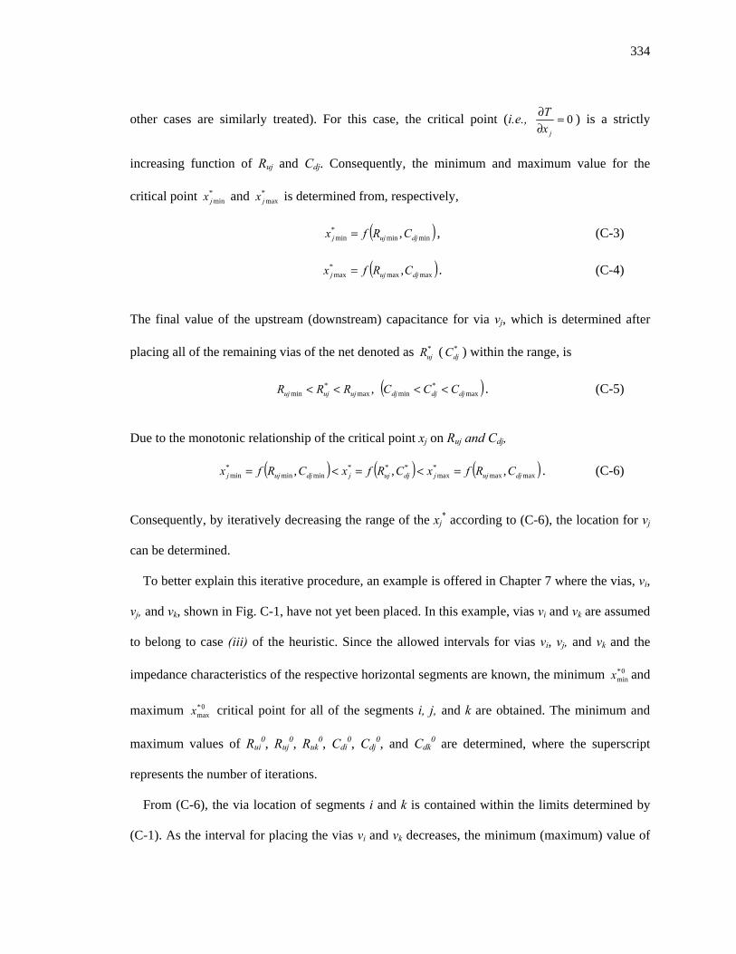
334
other cases are similarly treated). For this case, the critical point (i.e., 0=∂∂
jxT ) is a strictly
increasing function of Ruj and Cdj. Consequently, the minimum and maximum value for the
critical point *minjx and *
maxjx is determined from, respectively,
( )minmin*
min , djujj CRfx = , (C-3)
( )maxmax*
max , djujj CRfx = . (C-4)
The final value of the upstream (downstream) capacitance for via vj, which is determined after
placing all of the remaining vias of the net denoted as *ujR ( *
djC ) within the range, is
( )max*
minmax*
min , djdjdjujujuj CCCRRR <<<< . (C-5)
Due to the monotonic relationship of the critical point xj on Ruj and Cdj,
( ) ( ) ( )maxmax*
max***
minmin*
min ,,, djujjdjujjdjujj CRfxCRfxCRfx =<=<= . (C-6)
Consequently, by iteratively decreasing the range of the xj* according to (C-6), the location for vj
can be determined.
To better explain this iterative procedure, an example is offered in Chapter 7 where the vias, vi,
vj, and vk, shown in Fig. C-1, have not yet been placed. In this example, vias vi and vk are assumed
to belong to case (iii) of the heuristic. Since the allowed intervals for vias vi, vj, and vk and the
impedance characteristics of the respective horizontal segments are known, the minimum 0*minx and
maximum 0*maxx critical point for all of the segments i, j, and k are obtained. The minimum and
maximum values of Rui0, Ruj
0, Ruk0, Cdi
0, Cdj0, and Cdk
0 are determined, where the superscript
represents the number of iterations.
From (C-6), the via location of segments i and k is contained within the limits determined by
(C-1). As the interval for placing the vias vi and vk decreases, the minimum (maximum) value of

335
the upstream resistance and downstream capacitance of segment j increases (decreases), i.e.,
,1min
0min ujuj RR < ,1
min0
min djdj CC < ,0max
1max ujuj RR < and .0
max1
max djdj CC < Due to the monotonicity of xj* (see
(C-2)-(C-4) and (C-6)) on Ruj and Cdj, 1*min
0*min jj xx < and .0*
max1*max jj xx < The range of values for xj
*
therefore also decreases and, typically, after two or three iterations, the optimum location for the
corresponding via is determined.
The above example is extended to each of the other possible cases that can occur for segments i
and k. Specifically,
(a) i and k belong to either case (i) or (ii). Both Ruj and Cdj are precisely determined or,
equivalently, maxmin ujuj RR = and .maxmin djdj CC = Consequently, the placement of both vias vi and
vk is known and 0*minjx = 0*
maxjx = .*jx The placement of vj is also determined within the first
iteration.
(b) i belongs to case (i) or (ii) and k belongs to case (iii). Ruj is precisely determined or,
equivalently, maxmin ujuj RR = and the placement of via vi is known. Since vi is placed and k
belongs to case (iii), 1min
0min djdj CC < and 0
max1
max djdj CC < . The placement of via vj converges faster,
as only the placement of segment k remains unknown after the first iteration.
(c) k belongs to case (i) or (ii) and i belongs to case (iii). Cdj is precisely determined or,
equivalently, maxmin djdj CC = and the placement of via vk is known. Since vk is placed and i
belongs to case (iii), 1min
0min ujuj RR < and 0
max1
max ujuj RR < . The placement of via vj converges
faster as only the placement of segment i remains unknown after the first iteration.
(d) i belongs to any of the cases (i)-(iii) and k belongs to case (iv). Ruj is readily determined
(cases (i) and (ii)) or converges, as described in the previous example, 1min
0min ujuj RR < and
.0max
1max ujuj RR < As k belongs to case (iv), however, Cdj does not change as in the cases above. If
the decrease in the upstream resistance is sufficient to determine *jx according to (C-1), vj is
marked as processed, otherwise vj is marked as unprocessed and the algorithm continues to
the next via. In the latter case, the placement approach is described by case (iv) of the
heuristic.

336
(e) k belongs to any of the cases (i)-(iii) and i belongs to case (iv). Cdj is readily determined
(cases (i) and (ii)) or converges, as described in the previous example, implying 1min
0min djdj CC <
and 0max
1max djdj CC < . As i belongs to case (iv), however, Ruj does not change as in the
aforementioned cases. Overall, if the decrease in the downstream capacitance is sufficient to
determine *jx according to (C-1), vj is marked as processed, otherwise vj is marked as
unprocessed and the algorithm continues to the next via. In the latter case, the placement
approach is described by case (iv) of the heuristic.
(f) Both i and k belong to case (iv). Therefore, both Ruj and Cdj cannot be bounded.
Consequently, vj is marked as unprocessed and the next via is processed. Alternatively, this
sub-case degenerates to case (iv) of the heuristic presented in Chapter 7.

337
Appendix D: Proof of Condition for Via
Placement of Multi-Terminal Nets In this appendix, a proof for necessary condition 1 is provided.
v0 vi
vj
vk
lde
lds
ldn
xjth plane
(j+1)th plane
v0 vi
vj
vk
lde
lds
ldn
xjth plane
(j+1)th plane
Fig. D-1 A portion of an interconnect tree.
Condition 1: If rj > rj+1, only a type-1 move for vj can reduce the delay of a tree.
Proof: Consider Fig. D-, where the interplane via vj (the solid square) can be placed in any
direction de, ds, and dn within the interval lde, lds, and ldn, respectively. For the tree shown in Fig.
D-1 and removing the terms that are independent of vj, (8-1) is
( )
( ) ,2
2
0
⎟⎟⎟
⎠
⎞
⎜⎜⎜
⎝
⎛++++
+=
∑
∑ ∑
∈
∈ ∈
jvjj
jjjjjjjjvpsp
p
jijjj
ijUpspp
lcrClrClcRw
ClcRwT
vv
dvvdvvuPs
s
Uvdvv
Psuijsw
(D-1)
where
( )nsekjj dddj
kddvd lllcCC +++= +
∀∑ 1 . (D-2)

338
Suppose that a type-2 move is required, shifting vj by x towards the de direction (the dashed
square). Expression (8-1) becomes
( ) ( )[
( ) ( ) ( )] ⎥⎥⎥⎥
⎦
⎤
⎢⎢⎢⎢
⎣
⎡
++++−+
−+++⎟⎟
⎠
⎞
⎜⎜
⎝
⎛+
=
++
+∈∈ ∈∈∑∑ ∑∑
2211
1'
2121 xcrlcrClcxrlcClr
xCrrwCxclcRwRwT
jjvvdvvjdjddj
djjPs
sdjvvUv
uPs
sPs
uijs
jvjjjjjeje
jjvpsp
pjjjiji
jjvpsp
p
ijUpspp
w. (D-3)
For a type-2 move to reduce the weighted delay of the tree, shifting vj should decrease Tw, or,
equivalently, 0' <−=∆ ww TTT . Subtracting (D-1) from (D-3) yields
( )
( )⎪⎪⎪
⎭
⎪⎪⎪
⎬
⎫
⎪⎪⎪
⎩
⎪⎪⎪
⎨
⎧
+⎥⎥⎦
⎤+−+
⎢⎢⎣
⎡⎟⎟⎠
⎞⎜⎜⎝
⎛−+++
=∆
∑ ∑
∑
∈ ∈+
++
∈
iji ijUpsppj
ejejjjj
jvpspp
Uvj
Psuijs
jjjdjj
djddjjudvvj
Pss
xcRwxcr
xCrr
lcClrxcRClcxrw
T
2
22
1
11
. (D-4)
Since rj > rj+1, and 21 edj
dj
lcC +> from (D-2), (D-3) is always positive and a type-2 move cannot
reduce the delay of a tree.