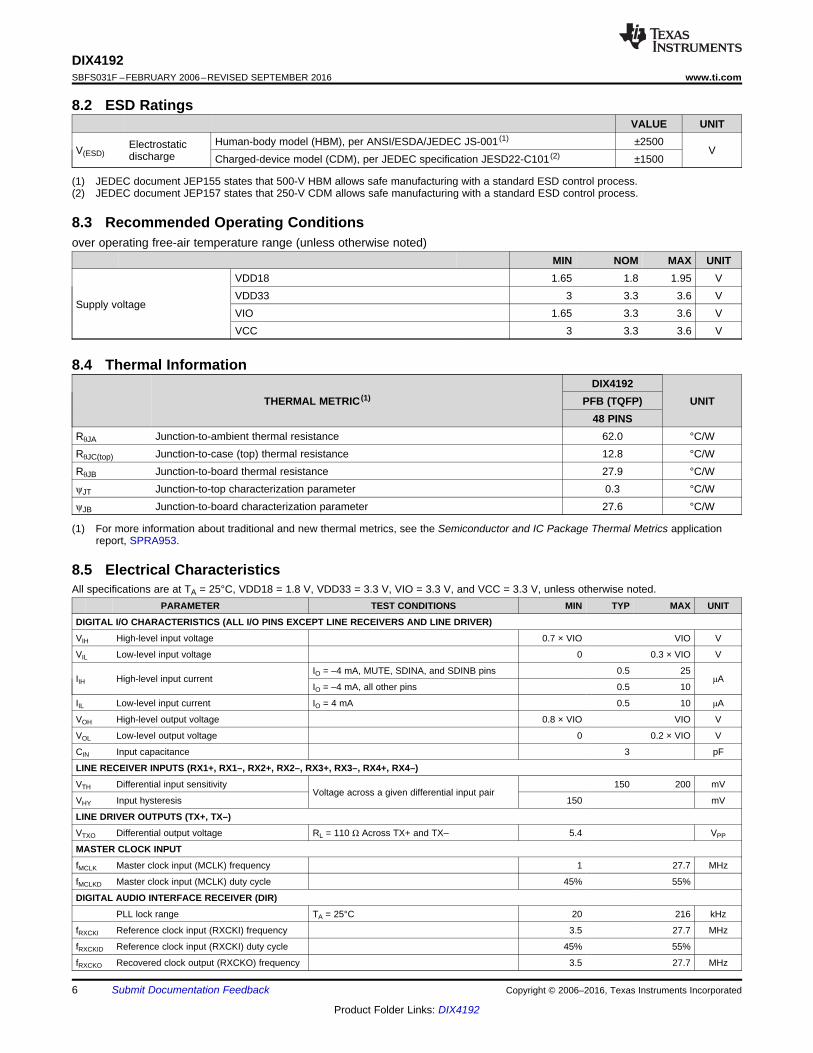
integrated digital audio interface receiver and ... · s/pdif in dix4192 x4 dsp s/pdif out pcm x1...
TRANSCRIPT

S/PDIFIN
DIX4192
DSPx4
S/PDIFOUT
PCM x1
GPO/INT
I2Cx1
PCM5242
PCM x1
TPA6120A2
Product
Folder
Sample &Buy
Technical
Documents
Tools &
Software
Support &Community
An IMPORTANT NOTICE at the end of this data sheet addresses availability, warranty, changes, use in safety-critical applications,intellectual property matters and other important disclaimers. PRODUCTION DATA.
DIX4192SBFS031F –FEBRUARY 2006–REVISED SEPTEMBER 2016
DIX4192 Integrated Digital Audio Interface Receiver and Transmitter
1
1 Features1• Digital Audio Interface Transmitter (DIT)
– Supports Sampling Rates Up to 216 kHz– Includes Differential Line Driver and
CMOS-Buffered Outputs• Digital Audio Interface Receiver (DIR)
– PLL Lock Range Includes Sampling Ratesfrom 20 kHz to 216 kHz
– Four Differential-Input Line Receivers and anInput Multiplexer
– Bypass Multiplexer Routes Line ReceiverOutputs to Line Driver and Buffer Outputs
– Automatic Detection of Non-PCM AudioStreams (DTS CD/LD and IEC 61937 formats)
– Audio CD Q-Channel Sub-Code Decoding andData Buffer
– Low Jitter Recovered Clock Output• User-Selectable Serial Host Interface: SPI™ or
I2C– Provides Access to On-Chip Registers and
Data Buffers– Status Registers and Interrupt Generation for
Flag and Error Conditions– Block-Sized Data Buffers for Both Channel
Status and User Data• Two Audio Serial Ports (Ports A and B)
– Synchronous Serial Interface to ExternalSignal Processors, Data Converters, and Logic
– Slave or Master Mode Operation WithSampling Rates Up to 216 kHz
– Supports Left-Justified, Right-Justified, andPhilips I2S™ Data Formats
– Supports Audio Data Word Lengths Up to24 Bits
• Four General-Purpose Digital Outputs– Multifunction Programmable Through Control
Registers• Extensive Power-Down Support
– Functional Blocks May Be DisabledIndividually When Not In Use
• Operates From 1.8-V Core and 3.3-V I/O PowerSupplies
• Small TQFP-48 Package, Compatible With theSRC4382 and SRC4392
2 Applications• Digital Audio Recorders and Mixing Desks• Digital Audio Interfaces for Computers• Digital Audio Routers and Distribution Systems• Broadcast Studio Equipment• DVD and CD Recorders• Surround Sound Decoders and A/V Receivers• Car Audio Systems
3 DescriptionThe DIX4192 device is a highly-integrated CMOSdevice designed for use in professional andbroadcast digital audio systems. The DIX4192combines a digital audio interface receiver (DIR) andtransmitter (DIT), two audio serial ports, and flexibledistribution logic for interconnection of the functionblock data and clocks.
The DIR and DIT are compatible with the AES3,S/PDIF, IEC 60958, and EIAJ CP-1201 interfacestandards. The audio serial ports and DIT may beoperated at sampling rates up to 216 kHz. The DIRlock range includes sampling rates from 20 kHz to216 kHz.
Device Information(1)
PART NUMBER PACKAGE BODY SIZE (NOM)DIX4192 TQFP (48) 7.00 mm × 7.00 mm
(1) For all available packages, see the orderable addendum atthe end of the data sheet.
DIX4192 Typical Application

2
DIX4192SBFS031F –FEBRUARY 2006–REVISED SEPTEMBER 2016 www.ti.com
Product Folder Links: DIX4192
Submit Documentation Feedback Copyright © 2006–2016, Texas Instruments Incorporated
Table of Contents1 Features .................................................................. 12 Applications ........................................................... 13 Description ............................................................. 14 Revision History..................................................... 25 Description (continued)......................................... 36 Device Comparison Table ..................................... 37 Pin Configuration and Functions ......................... 48 Specifications......................................................... 5
8.1 Absolute Maximum Ratings ...................................... 58.2 ESD Ratings.............................................................. 68.3 Recommended Operating Conditions....................... 68.4 Thermal Information .................................................. 68.5 Electrical Characteristics........................................... 68.6 Timing Requirements ................................................ 78.7 Typical Characteristics ............................................ 10
9 Detailed Description ............................................ 119.1 Overview ................................................................. 119.2 Functional Block Diagram ....................................... 129.3 Feature Description................................................. 12
9.4 Device Functional Modes........................................ 239.5 Register Maps ........................................................ 26
10 Application and Implementation........................ 5110.1 Application Information.......................................... 5110.2 Typical Application ................................................ 58
11 Power Supply Recommendations ..................... 5912 Layout................................................................... 60
12.1 Layout Guidelines ................................................. 6012.2 Layout Example .................................................... 60
13 Device and Documentation Support ................. 6113.1 Device Support...................................................... 6113.2 Documentation Support ........................................ 6113.3 Receiving Notification of Documentation Updates 6113.4 Community Resources.......................................... 6113.5 Trademarks ........................................................... 6113.6 Electrostatic Discharge Caution............................ 6213.7 Glossary ................................................................ 62
14 Mechanical, Packaging, and OrderableInformation ........................................................... 62
4 Revision HistoryNOTE: Page numbers for previous revisions may differ from page numbers in the current version.
Changes from Revision E (April 2016) to Revision F Page
• Changed fMCLK Max value From: 2.27 To: 27.7 ..................................................................................................................... 6
Changes from Revision D (January 2016) to Revision E Page
• Changed "IIH High-level input current" MAX value From: 10 µA To: 25 µA in the Electrical Characteristics table ................ 6• Changed Byte 2 in Figure 22a) Current Address Read, .. .................................................................................................. 25
Changes from Revision C (June 2006) to Revision D Page
• Added ESD Ratings table, Feature Description section, Device Functional Modes section, Application andImplementation section, Power Supply Recommendations section, Layout section, Device and DocumentationSupport section, and Mechanical, Packaging, and Orderable Information section. .............................................................. 1

3
DIX4192www.ti.com SBFS031F –FEBRUARY 2006–REVISED SEPTEMBER 2016
Product Folder Links: DIX4192
Submit Documentation FeedbackCopyright © 2006–2016, Texas Instruments Incorporated
5 Description (continued)The DIX4192 device is configured using on-chip control registers and data buffers, which are accessed througheither a 4-wire serial peripheral interface (SPI) port, or a 2-wire Philips I2C bus interface. Status registers provideaccess to a variety of flag and error bits, which are derived from the various function blocks. An open-draininterrupt output pin is provided, and is supported by flexible interrupt reporting and mask options through controlregister settings. A master reset input pin is provided for initialization by a host processor or supervisoryfunctions.
The DIX4192 device requires a 1.8-V core logic supply, in addition to a 3.3-V supply for powering portions of theDIR, DIT, and line driver and receiver functions. A separate logic I/O supply supports operation from 1.65 V to3.6 V, providing compatibility with low voltage logic interfaces typically found on digital signal processors andprogrammable logic devices. The DIX4192 device is available in a lead-free, TQFP-48 package, and is pin- andregister-compatible with the Texas Instruments SRC4382 and SRC4392 products.
6 Device Comparison Table
PART NUMBER 1.8 V IO MULTI-CH PCM ADC PCM PORTS S/PDIF PORTS
DIX4192 Yes No No 2 4 differential Line IN and 1differential Line Out
PCM9211 No Yes Yes Up to 3 IN and up to 3Out
Up to 12 single-ended INand up to 2 single-ended
Out
DIX9211 No Yes No Up to 3 IN and up to 3Out
Up to 12 single-ended INand up to 2 single-ended
Out

36
35
34
33
32
31
30
29
28
27
26
25
SYNC
BLS
AESOUT
VDD33
TX+
TX-
DGND2
GPO4
GPO3
GPO2
GPO1
MCLK
BC
KB
LR
CK
B
SD
INB
SD
OU
TB
BG
ND
DG
ND
3
VIO
NC
SD
OU
TA
SD
INA
LR
CK
A
BC
KA
RX
CK
I
NC
NC
DG
ND
1
VD
D18
CP
M
CS
/A0
CC
LK
/SC
L
CD
IN/A
1
CD
OU
T/S
DA
INT
RS
T
1
2
3
4
5
6
7
8
9
10
11
12
RX1+
RX1-
RX2+
RX2-
RX3+
RX3-
RX4+
RX4-
VCC
AGND
LOCK
RXCKO
48 47 46 45 44 43 42 41 40 39 38
13 14 15 16 17 18 19 20 21 22 23
37
24
4
DIX4192SBFS031F –FEBRUARY 2006–REVISED SEPTEMBER 2016 www.ti.com
Product Folder Links: DIX4192
Submit Documentation Feedback Copyright © 2006–2016, Texas Instruments Incorporated
(1) I = Input, O = Output, PWR = Power, GND = Ground
7 Pin Configuration and Functions
PFB Package48-Pin TQFP
Top View
Pin FunctionsPIN
TYPE (1) DESCRIPTIONNAME NO.
AESOUT 34 O DIT buffered AES3-encoded data
AGND 10 GND DIR comparator and PLL power-supply ground
BCKA 37 I/O Audio serial Port A bit clock
BCKB 48 I/O Audio serial Port B bit clock
BGND 44 GND Substrate ground, connect to AGND (pin 10)
BLS 35 I/O DIT block start clock
CCLK or SCL 20 I Serial data clock for SPI mode or I2C mode
CDIN or A1 21 I SPI port serial data input or programmable slave address for I2C mode
CDOUT or SDA 22 I/O SPI port serial data output (tri-state output) or serial data I/O for I2C mode
CPM 18 I Control port mode, 0 = SPI mode, 1 = I2C mode
CS or A0 19 I Chip select (active low) for SPI mode or programmable slave address for I2C mode
DGND1 16 GND Digital core ground
DGND2 30 GND DIR line receiver bias and DIT line driver digital ground
DGND3 43 GND Logic I/O ground
GPO1 26 O General-purpose output 1
GPO2 27 O General-purpose output 2
GPO3 28 O General-purpose output 3
GPO4 29 O General-purpose output 4

5
DIX4192www.ti.com SBFS031F –FEBRUARY 2006–REVISED SEPTEMBER 2016
Product Folder Links: DIX4192
Submit Documentation FeedbackCopyright © 2006–2016, Texas Instruments Incorporated
Pin Functions (continued)PIN
TYPE (1) DESCRIPTIONNAME NO.
INT 23 O Interrupt flag (open-drain, active low)
LOCK 11 O DIR PLL lock flag (active low)
LRCKA 38 I/O Audio serial Port A Left/Right clock
LRCKB 47 I/O Audio serial Port B left/right clock
MCLK 25 I Master clock
NC 14, 15, 41 — No internal signal connection, internally bonded to ESD pad
RST 24 I Reset (active low)
RX1+ 1 I Line receiver 1, noninverting input
RX1– 2 I Line receiver 1, inverting input
RX2+ 3 I Line receiver 2, noninverting input
RX2– 4 I Line receiver 2, inverting input
RX3+ 5 I Line receiver 3, noninverting input
RX3– 6 I Line receiver 3, inverting input
RX4+ 7 I Line receiver 4, noninverting input
RX4– 8 I Line receiver 4, inverting input
RXCKI 13 I DIR reference clock
RXCKO 12 O DIR recovered master clock (tri-state output)
SDINA 39 I Audio serial Port A data input
SDINB 46 I Audio serial Port B data input
SDOUTA 40 O Audio serial Port A data output
SDOUTB 45 O Audio serial Port B data output
SYNC 36 O DIT internal sync clock
TX+ 32 O DIT line driver noninverting output
TX– 31 O DIT line driver inverting output
VCC 9 PWR DIR comparator and PLL power supply, 3.3-V nominal
VDD18 17 PWR Digital core supply, 1.8-V nominal
VDD33 33 PWR DIR line receiver bias and DIT line driver supply, 3.3-V nominal
VIO 42 PWR Logic I/O supply, 1.65 V to 3.6 V
(1) Stresses beyond those listed under Absolute Maximum Ratings may cause permanent damage to the device. These are stress ratingsonly, which do not imply functional operation of the device at these or any other conditions beyond those indicated under RecommendedOperating Procedures. Exposure to absolute-maximum-rated conditions for extended periods may affect device reliability.
8 Specifications
8.1 Absolute Maximum Ratingsover operating free-air temperature range (unless otherwise noted) (1)
MIN MAX UNIT
Power supply
VDD18 –0.3 2 VVDD33 –0.3 4 VVIO –0.3 4 VVCC –0.3 4 V
Digital input voltage:digital logic
RXCKI, CPM, CS, CCLK, CDIN, CDOUT, INT, RST, MCLK, BLS, SYNC,BCKA, BCKB, LRCKA, LRCKB, SDINA, SDINB –0.3 (VIO + 0.3) V
Line receiver inputvoltage (per pin)
RX1+, RX1–, RX2+, RX2–, RX3+, RX3–, RX4+, RX4– (VDD33 + 0.3) VPP
Input current (all pins except power and ground) ±10 mAAmbient operating temperature –40 85 °CStorage temperature, Tstg –65 150 °C
6
DIX4192SBFS031F –FEBRUARY 2006–REVISED SEPTEMBER 2016 www.ti.com
Product Folder Links: DIX4192
Submit Documentation Feedback Copyright © 2006–2016, Texas Instruments Incorporated
(1) JEDEC document JEP155 states that 500-V HBM allows safe manufacturing with a standard ESD control process.(2) JEDEC document JEP157 states that 250-V CDM allows safe manufacturing with a standard ESD control process.
8.2 ESD RatingsVALUE UNIT
V(ESD)Electrostaticdischarge
Human-body model (HBM), per ANSI/ESDA/JEDEC JS-001 (1) ±2500V
Charged-device model (CDM), per JEDEC specification JESD22-C101 (2) ±1500
8.3 Recommended Operating Conditionsover operating free-air temperature range (unless otherwise noted)
MIN NOM MAX UNIT
Supply voltage
VDD18 1.65 1.8 1.95 VVDD33 3 3.3 3.6 VVIO 1.65 3.3 3.6 VVCC 3 3.3 3.6 V
(1) For more information about traditional and new thermal metrics, see the Semiconductor and IC Package Thermal Metrics applicationreport, SPRA953.
8.4 Thermal Information
THERMAL METRIC (1)DIX4192
UNITPFB (TQFP)48 PINS
RθJA Junction-to-ambient thermal resistance 62.0 °C/WRθJC(top) Junction-to-case (top) thermal resistance 12.8 °C/WRθJB Junction-to-board thermal resistance 27.9 °C/WψJT Junction-to-top characterization parameter 0.3 °C/WψJB Junction-to-board characterization parameter 27.6 °C/W
8.5 Electrical CharacteristicsAll specifications are at TA = 25°C, VDD18 = 1.8 V, VDD33 = 3.3 V, VIO = 3.3 V, and VCC = 3.3 V, unless otherwise noted.
PARAMETER TEST CONDITIONS MIN TYP MAX UNIT
DIGITAL I/O CHARACTERISTICS (ALL I/O PINS EXCEPT LINE RECEIVERS AND LINE DRIVER)
VIH High-level input voltage 0.7 × VIO VIO V
VIL Low-level input voltage 0 0.3 × VIO V
IIH High-level input currentIO = –4 mA, MUTE, SDINA, and SDINB pins 0.5 25
μAIO = –4 mA, all other pins 0.5 10
IIL Low-level input current IO = 4 mA 0.5 10 μA
VOH High-level output voltage 0.8 × VIO VIO V
VOL Low-level output voltage 0 0.2 × VIO V
CIN Input capacitance 3 pF
LINE RECEIVER INPUTS (RX1+, RX1–, RX2+, RX2–, RX3+, RX3–, RX4+, RX4–)
VTH Differential input sensitivityVoltage across a given differential input pair
150 200 mV
VHY Input hysteresis 150 mV
LINE DRIVER OUTPUTS (TX+, TX–)
VTXO Differential output voltage RL = 110 Ω Across TX+ and TX– 5.4 VPP
MASTER CLOCK INPUT
fMCLK Master clock input (MCLK) frequency 1 27.7 MHz
fMCLKD Master clock input (MCLK) duty cycle 45% 55%
DIGITAL AUDIO INTERFACE RECEIVER (DIR)
PLL lock range TA = 25°C 20 216 kHz
fRXCKI Reference clock input (RXCKI) frequency 3.5 27.7 MHz
fRXCKID Reference clock input (RXCKI) duty cycle 45% 55%
fRXCKO Recovered clock output (RXCKO) frequency 3.5 27.7 MHz

7
DIX4192www.ti.com SBFS031F –FEBRUARY 2006–REVISED SEPTEMBER 2016
Product Folder Links: DIX4192
Submit Documentation FeedbackCopyright © 2006–2016, Texas Instruments Incorporated
Electrical Characteristics (continued)All specifications are at TA = 25°C, VDD18 = 1.8 V, VDD33 = 3.3 V, VIO = 3.3 V, and VCC = 3.3 V, unless otherwise noted.
PARAMETER TEST CONDITIONS MIN TYP MAX UNIT
(1) The typical VIO supply current is measured using the DIX4192EVM evaluation module with loading from the DAIMB mother-boardcircuitry. VIO supply current is dependent upon the loading on the logic output pins.
fRXCKOD Recovered clock output (RXCKO) duty cycle 45% 55%
Recovered clock output (RXCKO) intrinsicjitter Measured cycle-to-cycle 250 ps RMS
DIGITAL AUDIO INTERFACE TRANSMITTER (DIT)
Intrinsic output jitter Measured cycle-to-cycle 200 ps RMS
POWER SUPPLIES
Supply current: initial startup
All blocks powered down by default
IDD18S VDD18 = 1.8 V 10 μA
IDD33S VDD33 = 3.3 V 10 μA
IIOS VIO = 3.3 V 300 μA
ICCS VCC = 3.3 V 10 μA
Supply current: quiescent
All blocks powered up with no clocks applied
IDD18Q VDD18 = 1.8 V 2.3 mA
IDD33Q VDD33 = 3.3 V 0.6 mA
IIOQ VIO = 3.3 V 0.3 mA
ICCQ VCC = 3.3 V 6.3 mA
Supply current: dynamic
All blocks powered up, fS = 48 kHz
IDD18D VDD18 = 1.8 V 5.1 mA
IDD33D VDD33 = 3.3 V 14.1 mA
IIOD (1) VIO = 3.3 V 46 mA
ICCD VCC = 3.3 V 7.4 mA
Supply current: high sampling rate
All blocks powered up, fS = 192 kHz
IDD18H VDD18 = 1.8 V 6.7 mA
IDD33H VDD33 = 3.3 V 15 mA
IIOH (1) VIO = 3.3 V 47 mA
ICCH VCC = 3.3 V 7.5 mA
Total power dissipation: initial startup All blocks powered down by default 1 mW
Total power dissipation: quiescent All blocks powered up with no clocks applied 28 mW
Total power dissipation: dynamic All blocks powered up, fS = 48 kHz 233 mW
Total power dissipation: high sampling rate All blocks powered up, fS = 192 kHz 242 mW
8.6 Timing RequirementsMIN NOM MAX UNIT
AUDIO SERIAL PORTS (PORT A AND PORT B)fLRCK LRCK clock frequency 0 216 kHztLRCKD LRCK clock duty cycle 50%fBCK BCK clock frequency 0 13.824 MHztBCKH BCK high pulse width 10 nstBCKL BCK low pulse width 10 nstAIS Audio data Input (SDIN) set-up time 10 nstAISH Audio data input (SDIN) hold time 10 nstADD Audio data output (SDOUT) delay 10 nsHOST INTERFACE: SPI MODEfCCLK Serial clock (CCLK) frequency 0 40 MHztCSCR CS falling to CCLK rising 8 nstCFCS CCLK falling to CS rising 7 nstCDS CDIN data set-up time 7 ns

8
DIX4192SBFS031F –FEBRUARY 2006–REVISED SEPTEMBER 2016 www.ti.com
Product Folder Links: DIX4192
Submit Documentation Feedback Copyright © 2006–2016, Texas Instruments Incorporated
Timing Requirements (continued)MIN NOM MAX UNIT
(1) All values referred to the VIH minimum and VIL maximum levels listed in the Digital I/O Characteristics section of this table.(2) A device must internally provide a hold time of at least 300 ns for the SDA signal (referred to the VIH minimum input level) to bridge the
undefined region of the falling edge of SCL.(3) The maximum tHDDAT has only to be met if the device does not stretch the Low period (tLOW) of the SCL signal.(4) A Fast mode I2C bus device can be used in a Standard mode I2C bus system, but the requirement that tSUDAT be 250 ns (minimum)
must then be met. For the DIX4192, this condition is automatically the case, because the device does not stretch the Low period of theSCL signal.
(5) CB is defined as the total capacitance of one bus line in picofarads (pF). If mixed with High-Speed mode devices, faster fall times areallowed.
tCDH CDIN data hold time 6 nstCFDO CCLK falling to CDOUT data valid 3 nstCSZ CS rising to CDOUT high-impedance, 3 nsHOST INTERFACE: I2C STANDARD MODE (1)
fSCL SCL clock frequency 0 100 kHztHDSTA Hold time repeated START condition 4 μstLOW Low period of SCL clock 4.7 μstHIGH High period of SCL clock 4 μstSUSTA Set-up time repeated START condition 4.7 μstHDDAT Data hold time 0 (2) 3.45 (3) μstSUDAT Data set-up time 250 nstR Rise time for both SDA and SDL 1000 nstF Fall time for both SDA and SDL 300 nstSUSTO Set-up time for STOP condition 4 μstBUF Bus free time between START and STOP 4.7 μsCB Capacitive load for each bus line 400 pFVNL Noise margin at low level (including hysteresis) 0.1 × VIO VVNH Noise margin at high level (including hysteresis) 0.2 × VIO VHOST INTERFACE: I2C FAST MODE (1)
fSCL SCL clock frequency 0 400 kHztHDSTA Hold time repeated START condition 0.6 μstLOW Low period of SCL clock 1.3 μstHIGH High period of SCL clock 0.6 μstSUSTA Set-up time repeated START condition 0.6 μstHDDAT Data hold time 0 (2) 0.9 (3) μstSUDAT Data set-up time 100 (4) nstR Rise time for both SDA and SDL 20 + 0.2CB
(5)300 ns
tF Fall time for both SDA and SDL 20 + 0.2CB(5)
300 ns
tSUSTO Set-up time for STOP condition 0.6 μstBUF Bus free time between START and STOP 1.3 μstSP Spike pulse width suppressed by input filter 0 50 nsCB Capacitive load for each bus Line 400 pFVNL Noise margin at low level (including hysteresis) 0.1 × VIO VVNH Noise margin at high level (including hysteresis) 0.2 × VIO V

SDA
SCL
S R P S
tF
tHDSTA
tLOW
tR
tHDDAT
tSUDAT
tF
tBUF
S = Start nCo dition R = Repea ed Startt Condition P = Stop Co ditionn
tSUSTA
tSUSTO
tHDSTA
tSP
tR
tHIGH
CS
CC KL
CD NI
CDOUT
tCFCS
tCDH
Hi Z Hi Z
tCSCR
tCDS
tCFDO
tCSZ
LRCK
BCK
SDIN
tAIS
SDOUT
tAIH
tAOD
tBCKL
tBCKH
9
DIX4192www.ti.com SBFS031F –FEBRUARY 2006–REVISED SEPTEMBER 2016
Product Folder Links: DIX4192
Submit Documentation FeedbackCopyright © 2006–2016, Texas Instruments Incorporated
Figure 1. Audio Serial Port Timing
Figure 2. SPI Timing
Figure 3. I2C Standard and Fast Mode Timing

2
0
-2
-4
-6
-8
-10
-12
-14
-16
-18
-20
100
101
102
103
Jitter Frequency (Hz)
104
105
106
Jitte
r A
tte
nu
atio
n (
dB
)
Peak J
itte
r (U
I)
-10
-20
-30
-40
-50
-60
-70
-80
-90
-100
-110
-120
-130
-140
-150
20 100 1k
Sinusoidal Jitter Frequency (Hz)
10k 100k
TH
D+
N R
atio (
dB
)
5
2
1
500m
200m
100m
50m
20m
10m
5m
2m
1m
THD+N
Output Jitter Amplitude
Input Jitter Amplitude
10
DIX4192SBFS031F –FEBRUARY 2006–REVISED SEPTEMBER 2016 www.ti.com
Product Folder Links: DIX4192
Submit Documentation Feedback Copyright © 2006–2016, Texas Instruments Incorporated
8.7 Typical Characteristics
Figure 4. DIR Jitter Attenuation Characteristics Figure 5. DIR Jitter Tolerance Plot

11
DIX4192www.ti.com SBFS031F –FEBRUARY 2006–REVISED SEPTEMBER 2016
Product Folder Links: DIX4192
Submit Documentation FeedbackCopyright © 2006–2016, Texas Instruments Incorporated
9 Detailed Description
9.1 OverviewThe DIX4192 is an integrated digital audio interface receiver and transmitter (DIR and DIT). Two audio serialports, Port A and Port B, support input and output interfacing to external data converters, signal processors, andlogic devices. On-chip routing logic provides for flexible interconnection between the four functional blocks. Theaudio serial ports and DIT may be operated at sampling rates up to 216 kHz. The DIR is specified for a PLL lockrange that includes sampling rates from 20 kHz to 216 kHz. All function blocks support audio data word lengthsup to 24 bits.
The DIX4192 requires an external host processor or logic for configuration control. The DIX4192 includes a user-selectable serial host interface, which operates as either a 4-wire serial peripheral interface (SPI) port or a 2-wirePhilips I2C bus interface. The SPI port operates at bit rates up to 40 MHz. The I2C bus interface may be operatedin standard or fast modes, supporting operation at 100 kbps and 400 kbps, respectively. The SPI and I2Cinterfaces provide access to internal control and status registers, as well as the buffers used for the DIR and DITchannel status and user data.
The digital interface receiver (DIR) includes four differential input line receiver circuits, suitable for balanced orunbalanced cable interfaces. Interfacing to optical receiver modules and CMOS logic devices is also supported.The outputs of the line receivers are connected to a 1-of-4 data selector, referred to as the receiver inputmultiplexer, which is used to select one of the four line receiver outputs for processing by the DIR core. Theoutputs of the line receivers are also connected to a second data selector, the bypass multiplexer, which may beused to route input data streams to the DIT CMOS output buffer and differential line driver functions. Thisconfiguration provides a bypass signal path for AES3-encoded input data streams.
The DIR core decodes the selected input stream data and separates the audio, channel status, user, validity, andparity data. Channel status and user data is stored in block-sized buffers, which may be accessed through theSPI or I2C serial host interface, or routed directly to the general-purpose output pins (GPO1 through GPO4). Thevalidity and parity bits are processed to determine error status. The DIR core recovers a low jitter master clock,which may be used to generate word and bit clocks using on-chip or external logic circuitry.
The digital interface transmitter (DIT) encodes digital audio input data into an AES3-formatted output datastream. Two DIT outputs are provided, including a differential line driver and a CMOS output buffer. Both the linedriver and buffer include 1-of-2 input data selectors, which are used to choose either the output of the DIT AES3encoder, or the output of the bypass multiplexer. The line driver output is suitable for balanced or unbalancedcable interfaces, while the CMOS output buffer supports interfacing to optical transmitter modules and externallogic or line drivers. The DIT includes block-sized data buffers for both channel status and user data. Thesebuffers are accessed through either the SPI or I2C host interface, or may be loaded directly from the DIR channelstatus and user data buffers.
The DIX4192 includes four general-purpose digital outputs, or GPO pins. The GPO pins may be configured assimple logic outputs, which may be programmed to either a low or high state. Alternatively, the GPO pins may beconnected to one of 13 internal logic nodes, allowing them to serve as functional, status, or interrupt outputs. TheGPO pins provide added utility in applications where hardware access to selected internal logic signals may benecessary.
Functional Block Diagram shows a simplified functional block diagram for the DIX4192. Additional details foreach function block will be covered in respective sections of this data sheet.

DIR
_O
UT
PO
RT
_A
_IN
PO
RT
_B
_IN
Audio SerialPort A
Audio SerialPort B
DigitalInterface
Receiver (DIR)
DigitalInterface
Transmitter(DIT)
TX+TX-
SDINA
SDOUTA
LRCKA
BC AK
SDINB
SDOUTB
LRCKB
BC BK
CPMCS or A0CCLK or SCLCDIN or 1ACDOUT or SDAINTRST
HostInterface
(SPI or I C)2
andGene ar l-Purp so eOutputs
MasterCl cko
Distribution
MC KL
RXCKIFrom RXCKO
GP 1OGP 2OGP 3OGP 4O
AESOUT
RXCKO
LOCK
RX +2
RX -2RX +3
RX -3
RX +4
RX -4
RX +1
RX -1
BLS
SY CN
Control and StatusRegisters
DIR C and UData Buffers
DIT C and UData Buffers
DIX4192
Power
VDD18DGND1VDD33DGND2VIODGND3VCCAG DN
BG DNInternally Tied
to Substrate
PO
RT
AP
OR
T B
DIR
DIT
12
DIX4192SBFS031F –FEBRUARY 2006–REVISED SEPTEMBER 2016 www.ti.com
Product Folder Links: DIX4192
Submit Documentation Feedback Copyright © 2006–2016, Texas Instruments Incorporated
9.2 Functional Block Diagram
9.3 Feature Description
9.3.1 RESET OperationThe DIX4192 includes an asynchronous active low reset input, RST (pin 24), which may be used to initialize theinternal logic at any time. The reset sequence forces all registers and buffers to their default settings. The resetlow pulse width must be a minimum of 500 ns in length. The user must not attempt a write or read operationusing either the SPI or I2C port for at least 500 μs after the rising edge of RST. See Figure 6 for the reset timingsequence of the DIX4192.
In addition to reset input, the RESET bit in control register 0x01 may be used to force an internal reset, wherebyall registers and buffers are forced to their default settings. Refer to Control Registers for details regarding theRESET bit function.
Upon reset initialization, all functional blocks of the DIX4192 default to the power-down state, with the exceptionof the SPI or I2C host interface and the corresponding control registers. The user may then program the DIX4192to the desired configuration, and release the desired function blocks from the power-down state using thecorresponding bits in control register 0x01.

RST
0
1
500ns (min) 500 sm (min)
Write or Readvia
S I orP I C2
13
DIX4192www.ti.com SBFS031F –FEBRUARY 2006–REVISED SEPTEMBER 2016
Product Folder Links: DIX4192
Submit Documentation FeedbackCopyright © 2006–2016, Texas Instruments Incorporated
Feature Description (continued)
Figure 6. Reset Sequence Timing
9.3.2 Master and Reference ClocksThe DIX4192 includes two clock inputs, MCLK (pin 25) and RXCKI (pin 13). The MCLK clock input is typicallyused as the master clock source for the audio serial ports and/or the DIT. The MCLK may also be used as thereference clock for the DIR. The RXCKI clock input is typically used for the DIR reference clock source, althoughit may also be used as the master or reference clock source for the audio serial ports.
In addition to the MCLK and RXCKI clock sources, the DIR core recovers a master clock from the AES3-encoded input data stream. This clock is suitable for use as a master or system clock source in manyapplications. The recovered master clock output, RXCKO (pin 12), may be used as the master or reference clocksource for the audio serial ports and the DIT, as well as external audio devices.
The master clock frequency for the audio serial ports (Port A and Port B) depends on the Slave or Master modeconfiguration of the port. In Slave mode, the ports do not require a master clock because the left/right word andbit clocks are inputs, sourced from an external audio device serving as the serial bus timing master. In Mastermode, the serial ports derive the left/right word and bit clock outputs from the selected master clock source,MCLK, RXCKI, or RXCKO. The left/right word clock rate is derived from the selected master clock source usingone of four clock divider settings (divide by 128, 256, 384, or 512). Refer to Audio Serial Port Operation foradditional details.
The DIT always requires a master clock source, which may be either the MCLK input, or the DIR recovered clockoutput, RXCKO. Like the audio serial ports, the DIT output frame rate is derived from the selected master clockusing one of four clock divider settings (divide-by-128, -256, -384, or -512). Refer to Digital Interface Transmitter(DIT) Operation for additional details.
The DIR reference clock may be any frequency that meets the PLL1 set-up requirements, described in ControlRegisters. Typically, a common audio system clock rate, such as 11.2896 MHz, 12.288 MHz, 22.5792 MHz, or24.576 MHz, may be used for this clock.
TI recommends that the clock sources for MCLK and RXCKI input be generated by low-jitter crystal oscillators foroptimal performance. In general, phase-locked loop (PLL) clock synthesizers must be avoided, unless they aredesigned or specified for low clock jitter.

Master
Clock
Source
Master
Mo ed
Clock
Generation
Serial
Input
Serial
Output
MC KL
RXCKI
RXCKO
Audio Data
Internal Clocks
OUTS[1:0] MU ET F T[1:M 0]
M/S DIV 1:[ 0]CLK 1:[ 0]
SD NI A (pin 39) or SDINB (pin 4 )6
LRCKA (pin 3 ) or8 LRCKB ( i 47)p n
BCKA (pin 37) or BCKB (pin 48)
SDOUTA (pin 40) or SDOUTB (pin 45)
Da at
Source
Port A
Port B
DIR
14
DIX4192SBFS031F –FEBRUARY 2006–REVISED SEPTEMBER 2016 www.ti.com
Product Folder Links: DIX4192
Submit Documentation Feedback Copyright © 2006–2016, Texas Instruments Incorporated
Feature Description (continued)9.3.3 Audio Serial Port OperationThe DIX4192 includes two audio serial ports, Port A and Port B. Both ports are 4-wire synchronous serialinterfaces, supporting simultaneous input and output operation. Because each port has only one pair of left orright word and bit clocks, the input and output sampling rates are identical. A simplified block diagram is shown inFigure 7.
The audio serial ports may be operated at sampling rates up to 216 kHz, and support audio data word lengths upto 24 bits. Philips I2S, Left-Justified, and Right-Justified serial data formats are supported. Refer to Figure 8.
The left or right word clock (LRCKA or LRCKB) and the bit clock (BCKA or BCKB) may be configured for eitherMaster or Slave mode operation. In Master mode, these clocks are outputs, derived from the selected masterclock source using internal clock dividers. The master clock source may be 128, 256, 384, or 512 times the audioinput/output sampling rate, with the clock divider being selected using control register bits for each port. In Slavemode the left or right word and bit clocks are inputs, and are sourced from an external audio device acting as theserial bus master.
The LRCKA or LRCKB clocks operate at the input and output sampling rate, fS. The BCKA and BCKB clock ratesare fixed at 64 times the left or right word clock rate in Master mode. For Slave mode, the minimum BCKA andBCKB clock rate is determined by the audio data word length multiplied by two, because there are two audiodata channels per left or right word clock period. For example, if the audio data word length is 24 bits, the bitclock rate must be at least 48 times the left or right word clock rate, allowing one bit clock period for each data bitin the serial bit stream.
Serial audio data is clocked into the port on the rising edge of the bit clock, while data is clocked out of the porton the falling edge of the bit clock. Refer to the Audio Serial Ports section of the Electrical Characteristics tablefor parametric information and Figure 1 for a timing diagram related to audio serial port operation.
The audio serial ports are configured using control registers 0x03 through 0x06. Refer to Control Registers fordescriptions of the control register bits.
Figure 7. Audio Serial Port Block Diagram

MSB LSB MSB LSB
MSB LSB MSB LSB
LSBMSB LSBMSB
LRCKA
LRCKB
BC AK
BC BK
Audio
Da at
LRCKA
LRCKB
BC AK
BC BK
Audio
Da at
LRCKA
LRCKB
BC AK
BC BK
Audio
Da at
(a) Left-Justified Data For am t
(b) Right-Justif e Dai d ta Form ta
(c) I S Data Fo m tr a2
1/fs
Channel 1 (Left Channel) Channel 2 (Right Channel)
15
DIX4192www.ti.com SBFS031F –FEBRUARY 2006–REVISED SEPTEMBER 2016
Product Folder Links: DIX4192
Submit Documentation FeedbackCopyright © 2006–2016, Texas Instruments Incorporated
Feature Description (continued)
Figure 8. Audio Data Formats
9.3.4 Overview of the AES3 Digital Audio Interface ProtocolThis section introduces the basics of digital audio interface protocols pertaining to the transmitter (DIT) andreceiver (DIR) blocks of the DIX4192. Emphasis is placed upon defining the basic terminology andcharacteristics associated with the AES3-2003 standard protocol, the principles of which may also be applied toa number of consumer-interface variations, including S/PDIF, IEC-60958, and EIAJ CP-1201. It is assumed thatthe reader is familiar with the AES3 and S/PDIF interface formats. Additional information is available from thesources listed in the Development Support section.
The AES3-2003 standard defines a technique for two-channel linear PCM data transmission over 110-Ω shieldedtwisted-pair cable. The AES-3id document extends the AES3 interface to applications employing 75-Ω coaxialcable connections. In addition, consumer transmission variants, such as those defined by the S/PDIF, IEC60958, and CP-1201 standards, use the same encoding techniques but with different physical interfaces ortransmission media. Channel status data definitions also vary between professional and consumer interfaceimplementations.

X Channel 1 Y Channel 2 Channel 1Z Y Channel 2 X Channel 1 Y Channel 2
Frame 191 Frame 0 Frame 1
Block Start
One Sub Frame
Bits: 0 3 4 7 8 27 28 29 30 31
MSB V U C PPreamble Audio DataAudio or
Aux Data
Validity Bit
Use Dr ata
Channel Status Data
P rita y Bit
16
DIX4192SBFS031F –FEBRUARY 2006–REVISED SEPTEMBER 2016 www.ti.com
Product Folder Links: DIX4192
Submit Documentation Feedback Copyright © 2006–2016, Texas Instruments Incorporated
Feature Description (continued)For AES3 transmission, data is encoded into frames, with each frame containing two subframes of audio andstatus data, corresponding to audio Channels 1 and 2 (or Left and Right, respectively, for stereophonic audio).Figure 9 shows the AES3 frame and subframe formatting. Each subframe includes four bits for the preamble, upto 24 bits for audio and/or auxiliary data, one bit indicating data validity (V), one bit for channel status data (C),one bit for user data (U), and one bit for setting parity (P).
The 4-bit preamble is used for synchronization and identification of blocks and subframes. The X and Y preamblecodes are used to identify the start of the Channel 1 and Channel 2 subframes, as shown in Figure 9. However,the X preamble for the first subframe of every 192 frames is replaced by the Z preamble, which identifies thestart of a new block of channel status and user data.
Figure 9. AES3 Frame and Subframe Encoding
One block is comprised of 192 frames of data. This format translates to 192 bits each for channel status anduser data for each channel. The 192 bits are organized into 24 data bytes, which are defined by the AES3-2003and consumer standards documents. The AES18 standard defines recommended usage and formatting of theuser data bits, while consumer applications may use the user data for other purposes. The DIX4192 alsoincludes block-sized transmitter and receiver channel status and user data buffers, which have 24 bytes each forthe channel status and user data assigned to audio Channels 1 and 2. Refer to Channel Status and User DataBuffer Maps for the organization of the buffered channel status and user data for the receiver and transmitterfunctions.
The audio data for Channel 1 and Channel 2 may be up to 24 bits in length, and occupies bits 4 through 27 ofthe corresponding subframe. Bit 4 is the LSB while bit 27 is the MSB. If only 20 bits are required for audio data,then bits 8 through 27 are used for audio data, while bits 4 though 7 are used for auxiliary data bits.
The validity (V) bit indicates whether or not the audio sample word being transmitted is suitable for digital-to-analog (D/A) conversion or further digital processing at the receiver end of the connection. If the validity bit is 0,then the audio sample is suitable for conversion or additional processing. If the validity bit is 1, then the audiosample is not suitable for conversion or additional processing.
The parity (P) bit is set to either a 0 or 1, such that bits 4 through 31 carry an even number of ones and zeros foreven parity. The DIT block in the DIX4192 automatically manages the parity bit, setting it to a 0 or 1 as required.The DIR block checks the parity of bits 4 though 31 and generates a parity error if odd parity is detected.

Preceding state: 0 1
Preamble: Channel coding: Channel coding: Description:X 111 000 10 000 111 01 Channel su1 bframeY 111 010 00 000 101 11 Channel su2 bframeZ 111 100 00 000 011 11 Channel 1 subframe and block start
Cl cko
(2x Source Bi atet R )
Source Data Coding
(NR )Z
AES3 Channel Coding
(Biphase Mark)
Insert Preamble
Code Below
Preceding state, fr of the previous frameom the Parity bit .
Preamble Z (Block Start)
Preamble Coding
0
0
1
1
17
DIX4192www.ti.com SBFS031F –FEBRUARY 2006–REVISED SEPTEMBER 2016
Product Folder Links: DIX4192
Submit Documentation FeedbackCopyright © 2006–2016, Texas Instruments Incorporated
Feature Description (continued)The binary non-return to zero (NRZ) formatted audio and status source data for bits 4 through 31 of eachsubframe are encoded using a Biphase Mark format for transmission. This format allows for clock recovery at thereceiver end, as well as making the interface insensitive to the polarity of the balanced cable connections. Thepreambles at the start of each subframe are encoded to intentionally violate the Biphase Mark formatting, makingtheir detection by the receiver reliable, as well as avoiding the possibility of audio and status data imitating thepreambles. Figure 10 shows the Biphase Mark and preamble encoding.
Although the AES3 standard originally defined transmission for sampling rates up to 48 kHz, the interface iscapable of handling higher sampling rates, given that attention is paid to cable length and impedance matching.Equalization at the receiver may also be required, depending on the cable and matching factors. It is alsopossible to transmit and decode more than two channels of audio data using the AES3 or related consumerinterfaces. Special encoding and compression algorithms are used to support multiple channels, including theDolby® AC-3, DTS, MPEG-1/2, and other data reduced audio formats.
Figure 10. Biphase Mark Encoding
9.3.5 Digital Interface Transmitter (DIT) OperationThe DIT encodes a given two-channel or data-reduced audio input stream into an AES3-encoded output stream.In addition to the encoding function, the DIT includes differential line driver and CMOS-buffered output functions.The line driver is suitable for driving balanced or unbalanced line interfaces, while the CMOS-buffered output isdesigned to drive external logic or line drivers, as well as optical transmitter modules. Figure 11 shows thefunctional block diagram for the DIT.
The input of the DIT receives the audio data for Channels 1 and 2 from one of three possible sources: Port A,Port B, or the DIR. By default Port A is selected as the source. The DIT also requires a master clock source,which may be provided by either the MCLK input (pin 25) or RXCKO (the DIR recovered master clock output). Amaster clock divider is used to select the frame rate for the AES3-encoded output data. The TXDIV[1:0] bits incontrol register 0x07 are used to select divide by 128, 256, 384, or 512 operation.
Channel status and user data for Channels 1 and 2 are input to the AES3 encoder through the correspondingTransmitter Access (TA) data buffers. The TA data buffers are in turn loaded from the User Access (UA) buffers,which are programmed through the SPI or I2C host interface, or loaded from the DIR Receiver Access (RA) databuffers. The source of the channel status and user data is selected using the TXCUS[1:0] bits in control register0x09. When the DIR is selected as the input source, the channel status and user data output from the DIT isdelayed by one block in relation to the audio data.
The validity (V) bit may be programmed using one of two sources. The VALSEL bit in control register 0x09 isused to select the validity data source for the DIT block. The default source is the VALID bit in control register0x07, which is written through the SPI or I2C host interface. The validity bit may also be transferred from theAES3 decoder output of the DIR, where the V bit for the DIT subframes tracks the decoded DIR value frame byframe.

MCLK
RXCKO
User Access
(UA) Buffers
Transmitter Access
(TA) Buffers
Channel
Status
User
Data
From Receiver
Access (RA) Buffer
From Receiver
Access (RA) Buffer
To/From SPI or I C2
Host Interface
To/From SPI or I C2
Host Interface
TXCLK
TXCUS[1:0] TXBTD
TXIS[1:0]
BLS (pin 35)
SYNC (pin 36)
AE 3S
Encoder
AESMUX
LDMUX
AESOFF
TXOFF
From
Bypass
Multiplexer
Output
TX+ (pin 32)
TX (pin 31)-
AESOUT
(pin 34)
Master
Clock
Source
Da at
Source
Channel
Status
User
Da at
TXMUTE BL MS
Port A
Port B
DIR
TXDIV[1:0]
18
DIX4192SBFS031F –FEBRUARY 2006–REVISED SEPTEMBER 2016 www.ti.com
Product Folder Links: DIX4192
Submit Documentation Feedback Copyright © 2006–2016, Texas Instruments Incorporated
Feature Description (continued)The Parity (P) bit will always be generated by the AES3 encoder internal parity generator logic, such that bits 4through 31 of the AES3-encoded subframe are even parity.
The AES3 encoder output is connected to the output line driver and CMOS buffer source multiplexers. As shownin Figure 11, the source multiplexers allow the line driver or buffer to be driven by the AES3-encoded data fromthe DIT, or by the bypass multiplexer, which is associated with the outputs of the four differential input linereceivers preceding the DIR core. The bypass multiplexer allows for one of the four line receiver outputs to berouted to the line driver or buffer output, thereby providing a bypass mode of operation. Both the line driver andCMOS output buffer include output disables, set by the TXOFF and AESOFF bits in control register 0x08. Whenthe outputs are disabled, they are forced to a low logic state.
The AES3 encoder includes an output mute function that sets all bits for both the Channel 1 and 2 audio andauxiliary data to zero. The preamble, V, U, and C bits are unaffected, while the P bit is recalculated. The mutefunction is controlled using the TXMUTE bit in control register 0x08.
Figure 11. Digital Interface Transmitter (DIT) Functional Block Diagram
The AES3 encoder includes a block start input/output pin, BLS (pin 35). The BLS pin may be programmed as aninput or output. The input/output state of the BLS pin is programmed using the BLSM bit in control register 0x07.By default, the BLS pin is configured as an input.
As an input, the BLS pin may be used to force a block start condition, whereby the start of a new block ofchannel status and user data is initiated by generating a Z preamble for the next frame of data. The BLS inputmust be synchronized with the DIT internal SYNC clock. This clock is output on SYNC (pin 36). The SYNC clockrising edge is aligned with the start of each frame for the AES3-encoded data output by the DIT. Figure 12 showsthe format required for an external block start signal, as well as indicating the format when the BLS pin isconfigured as an output. When the BLS pin is an output, the DIT generates the block start signal based upon theinternal SYNC clock.
For details regarding DIT control and status registers, as well as channel status and user data buffers, refer toControl Registers and Channel Status and User Data Buffer Maps.

PL 1L
AE 3SDecoder
PulseGenerator
PL 2L128fS256fS512fS
ClockDivider
Divide by1, 2, 4, or 8
Data StreamDe-M xu
RX1+ (pin 1)
RX1 (pin 2)-
RX2+ (pin 3)
RX2 (pin 4)-
RX3+ (pin 5)
RX3 (pin 6)-
RX4+ (pin 7)
RX4 (pin 8)-
LOCK(pin 11)
RXCKO(pin 12)
RXCKO
BYPMUX[1 0: ]
R MUX[X 1:0]
RXCLK
MC KL
RXCKI
RXCKOF[1:0]
Ch 1.(Left)Audio
Ch 2.(Right)Audio
Cha nen lStatus
ChannelStatus
UserDa at
UserDa at
User Access(UA) Buffers
ReceiverAccess(RA) Buffers
ToDIT
To SPI or I C Host Interface2
ReceiverSy cn
GeneratorRCV_SYNC
Error andStatus Outputs
To DIT Bufferand Line Driver
ReferenceClock
Source
ToDIT
SY CN
BLS
(input)
BLS
(output)
Block Start
(Frame 0 starts here)
19
DIX4192www.ti.com SBFS031F –FEBRUARY 2006–REVISED SEPTEMBER 2016
Product Folder Links: DIX4192
Submit Documentation FeedbackCopyright © 2006–2016, Texas Instruments Incorporated
Feature Description (continued)
Figure 12. DIT Block Start Timing
9.3.6 Digital Interface Receiver (DIR) OperationThe DIR performs AES3 decoding and clock recovery and provides the differential line receiver functions. Thelock range of the DIR includes frame and sampling rates from 20 kHz to 216 kHz. Figure 13 shows the functionalblock diagram for the DIR.
Four differential line receivers are used for signal conditioning the encoded input data streams. The receivers canbe externally configured for either balanced or unbalanced cable interfaces, as well as interfacing with CMOSlogic level inputs from optical receivers or external logic circuitry. See Figure 14 for a simplified schematic for theline receiver. External connections are discussed in Receiver Input Interfacing.
Figure 13. Digital Interface Receiver (DIR) Functional Block Diagram

RX+
RX-
To Receiver
Input and Bypass
Multiplexers
24kW
VDD33
24kW
24kW 24kW
3kW
3kW
DGND2
20
DIX4192SBFS031F –FEBRUARY 2006–REVISED SEPTEMBER 2016 www.ti.com
Product Folder Links: DIX4192
Submit Documentation Feedback Copyright © 2006–2016, Texas Instruments Incorporated
Feature Description (continued)
Figure 14. Differential Line Receiver Circuit
The outputs of the four line receivers are connected to two 1-of-4 data selectors: the receiver input multiplexerand the bypass multiplexer. The input multiplexer selects one of the four line receiver outputs as the source forthe AES3-encoded data stream to be processed by the DIR core. The bypass multiplexer is used to route a linereceiver output to either the DIT line driver or CMOS-buffered outputs, thereby bypassing all other internalcircuitry. The bypass function is useful for simple signal distribution and routing applications.
The DIR requires a reference clock, supplied by an external source applied at either the RXCKI (pin 13) or MCLK(pin 25) clock inputs. PLL1 multiplies the reference clock to a higher rate, which is used as the oversamplingclock for the AES3 decoder. The decoder samples the AES3-encoded input stream in order to extract all of theaudio and status data. The decoded data stream is sent on to a de-multiplexer, where audio and status data areseparated for further processing and buffering. The pulse generator circuitry samples the encoded input datastream and generates a clock that is 16 times the frame/sampling rate (or fS). The 16 fS clock is then processedby PLL2, which further multiplies the clock rate and provides low-pass filtering for jitter attenuation. The availablePLL2 output clock rates include 512 fS, 256 fS, and 128 fS. The maximum available PLL2 output clock rate for agiven input sampling rate is estimated by internal logic and made available for readback through status register0x13.
The output of PLL2 may be divided by a factor of two, four, or eight, or simply passed through to the recoveredmaster clock output, RXCKO (pin 12). The RXCKO clock may also be routed internally to other function blocks,where it may be further divided to create left/right word and bit clocks. The RXCKO output may be disabled andforced to a high-impedance state by means of a control register bit, allowing other tri-state buffered clocks to betied to the same external circuit node, if required. By default, the RXCKO output (pin 12) is disabled and forcedto a high-impedance state.
Figure 15 shows the frequency response of PLL2. Jitter attenuation starts at approximately 50 kHz. Peaking isnominally 1 dB, which is within the 2 dB maximum allowed by the AES3 standard. The receiver jitter toleranceplot for the DIR is shown in Figure 16, along with the required AES3 jitter tolerance template. The DIR jittertolerance satisfies the AES3 requirements, as well as the requirements set forth by the IEC60958-3 specification.Figure 16 was captured using a full-scale 24-bit, two-channel, AES3-encoded input stream with a 48kHz framerate.
The decoded audio data, along with the internally-generated sync clocks, may be routed to other function blocks,including Port A, Port B, and the DIT. The decoded channel status and user data are buffered in thecorresponding Receiver Access (RA) data buffers, then transferred to the corresponding User Access (UA) databuffers, where it may be read back through either the SPI or I2C serial host interface. The contents of the RAbuffers may also be transferred to the DIT UA data buffers; this transfer is shown in Figure 11. The channelstatus and user data bits may also be output serially through the general-purpose output pins, GPO[4:1].Figure 17 shows the output format for the GPO pins when used for this purpose, along with the DIR block start(BLS) and frame synchronization (SYNC) clocks. The rising edges of the DIR SYNC clock output are aligned withthe start of each frame for the received AES3 data.

Ch 2.Ch. 1 Ch. 1Ch 2. Ch 2.Ch. 1 Ch. 1Ch 2.
BLS
(output)
SY CN
(output)
C or U da at
(output)
Bit 0 Bit 1 Bit 2 Bit 4 ¼
Block Start
(Fr mea 0 St rts Hea re)
2
0
-2
-4
-6
-8
-10
-12
-14
-16
-18
-20
100
101
102
103
Jitter Frequency (Hz)
104
105
106
Jitte
r A
ttenuation (
dB
)
Peak J
itte
r (U
I)
-10
-20
-30
-40
-50
-60
-70
-80
-90
-100
-110
-120
-130
-140
-150
20 100 1k
Sinusoidal Jitter Frequency (Hz)
10k 100k
TH
D+
N R
atio (
dB
)
5
2
1
500m
200m
100m
50m
20m
10m
5m
2m
1m
THD+N
Output Jitter Amplitude
Input Jitter Amplitude
21
DIX4192www.ti.com SBFS031F –FEBRUARY 2006–REVISED SEPTEMBER 2016
Product Folder Links: DIX4192
Submit Documentation FeedbackCopyright © 2006–2016, Texas Instruments Incorporated
Feature Description (continued)The DIR includes a dedicated, active low AES3 decoder and PLL2 lock output, named LOCK (pin 11). The lockoutput is active only when both the AES3 decoder and PLL2 indicate a lock condition. Additional DIR status flagsmay be output at the general-purpose output (GPO) pins, or accessed through the status registers through theSPI or I2C host interface. Refer to General-Purpose Digital Outputs and Control Registers for additionalinformation regarding the DIR status functions.
Figure 15. DIR Jitter Attenuation Characteristics Figure 16. DIR Jitter Tolerance Plot
Figure 17. DIR Channel Status and User Data Serial Output Format Through the GPO Pins

VIO
10kW
To the outputs fINT or
additional DIX4192 devices
Interrupt
Logic
DIX4192 MCU, DSP,
or Logic
INT 23 Interrupt
Input
22
DIX4192SBFS031F –FEBRUARY 2006–REVISED SEPTEMBER 2016 www.ti.com
Product Folder Links: DIX4192
Submit Documentation Feedback Copyright © 2006–2016, Texas Instruments Incorporated
Feature Description (continued)9.3.7 General-Purpose Digital OutputsThe DIX4192 includes four general-purpose digital outputs, GPO1 through GPO4 (pins 26 through 29,respectively). A GPO pin may be programmed to a static high or low state. Alternatively, a GPO pin may beconnected to one of 13 internal logic nodes, allowing the GPO pin to inherit the function of the selected signal.Control registers 0x1B through 0x1E are used to select the function of the GPO pins. For details regarding GPOoutput configuration, refer to Control Registers. Table 1 summarizes the available output options for the GPOpins.
Table 1. General-Purpose Output Pin ConfigurationsGPOn3 GPOn2 GPOn1 GPOn0 GPOn FUNCTION
0 0 0 0 GPOn is forced low (default)0 0 0 1 GPOn is forced high0 0 1 0 Reserved0 0 1 1 DIT interrupt flag; active low0 1 0 0 DIR interrupt flag; active low0 1 0 1 DIR 50/15-μs emphasis flag; active low0 1 1 0 DIR non-audio data flag; active high0 1 1 1 DIR non-valid data flag; active high1 0 0 0 DIR channel status data serial output1 0 0 1 DIR user data serial output1 0 1 0 DIR block start clock output
1 0 1 1 DIR COPY bit output(0 = copyright asserted, 1 = copyright not asserted)
1 1 0 0 DIR L (or origination) bit output(0 = 1st generation or higher, 1 = original)
1 1 0 1 DIR Parity error flag; active high
1 1 1 0 DIR internal sync clock output; may be used as the data clock for the channelstatus and user data serial outputs.
1 1 1 1 DIT internal sync clock
9.3.8 Interrupt OutputThe DIX4192 includes multiple internal status bits, many of which may be set to trigger an interrupt signal. Theinterrupt signal is output at INT (pin 23), which is an active low, open-drain output. The INT pin requires a pullupresistor to the VIO supply rail. The value of the pullup is not critical, but a 10-kΩ device must be sufficient formost applications. Figure 18 shows the interrupt output pin connection. The open-drain output allows interruptpins from multiple DIX4192 devices to be connected in a wired OR configuration.
Figure 18. Interrupt Output Pin Connections

CS
CD NI
CC KL
Set = 1 here to gister location.write/read one reCSHold = 0 to enab de.le auto-increment moCS
Byte 0 Byte 1 Byte 2 Byte 3 Byte N
R/W A6 A5 A0A4 A1A3 A2
Set to 0 for Write ad.; Set to or Re1 f
Byte 0:
MSB LSB
Byte Defi itionn
Header Register Data
Register Address
Byte 1: Don t Car’ e
Byte 2 through Byte N: Register D ta a
CDOUT Hi Z Hi Z Data for A[ : ]+16 0Data for A[6:0] Data for A[ : ]+N2 0
Register Data
23
DIX4192www.ti.com SBFS031F –FEBRUARY 2006–REVISED SEPTEMBER 2016
Product Folder Links: DIX4192
Submit Documentation FeedbackCopyright © 2006–2016, Texas Instruments Incorporated
9.4 Device Functional Modes
9.4.1 Host Interface Operation: Serial Peripheral Interface (SPI) ModeThe DIX4192 supports a 4-wire SPI port when the CPM input (pin 18) is forced low or tied to ground. The SPIport supports high-speed serial data transfers up to 40 Mbps. Register and data buffer write and read operationsare supported.
The CS input (pin 19) serves as the active low chip select for the SPI port. The CS input must be forced low inorder to write or read registers and data buffers. When CS is forced high, the data at the CDIN input (pin 21) isignored, and the CDOUT output (pin 22) is forced to a high-impedance state. The CDIN input serves as the serialdata input for the port; the CDOUT output serves as the serial data output.
The CCLK input (pin 20) serves as the serial data clock for both the input and output data. Data is latched at theCDIN input on the rising edge of CCLK, while data is clocked out of the CDOUT output on the falling edge ofCCLK.
Figure 19 shows the SPI port protocol. Byte 0 is referred to as the command byte, where the most significant bit(or MSB) is the read/write bit. For the R/W bit, a 0 indicates a write operation, while a 1 indicates a readoperation. The remaining seven bits of the command byte are used for the register address targeted by the writeor read operation. Byte 1 is a don’t care byte, and may be set to all zeroes. This byte is included in order toretain protocol compatibility with earlier Texas Instruments digital audio interface and sample rate converterproducts, including the DIT4096, DIT4192, the SRC418x series devices, and the SRC419x series devices.
The SPI port supports write and read operations for multiple sequential register addresses through theimplementation of an auto-increment mode. As shown in Figure 19, the auto-increment mode is invoked bysimply holding the CS input low for multiple data bytes. The register address is automatically incremented aftereach data byte transferred, starting with the address specified by the command byte.
Refer to the SPI section of the Electrical Characteristics table and Figure 2 for specifications and a timingdiagram that highlight the key parameters for SPI operation.
Figure 19. Serial Peripheral Interface (SPI) Protocol for the DIX4192

A6 A5 A4 A3 A2 A1 A0
1 1 1 0 0 A1 A0 R/W
Se yt b Pin 91
Se yt b Pin 12
MSB LSB
Fir ts Byte After o itthe RSTA T/RESTART C ond i n
Slave Address
A6 A5 A4 A3 A2 A1 A0INC
MSB LSB
(a) DIX419 lave2 S Address
(b) Regist r Addree ss Byte
Auto-In ecrem nt
0 = Disabled
1 = Enabled
24
DIX4192SBFS031F –FEBRUARY 2006–REVISED SEPTEMBER 2016 www.ti.com
Product Folder Links: DIX4192
Submit Documentation Feedback Copyright © 2006–2016, Texas Instruments Incorporated
Device Functional Modes (continued)9.4.2 Host Interface Operation: PHILIPS I2C ModeThe DIX4192 supports a 2-wire Philips I2C bus interface when CPM (pin 18) is forced high or pulled up to theVIO supply rail. The DIX4192 functions as a Slave-only device on the bus. Standard and Fast modes ofoperation are supported. Standard mode supports data rates up to 100 kbps, while Fast mode supports datarates up to 400 kbps. Fast mode is downward compatible with Standard mode, and these modes are sometimesreferred to as Fast/Standard, or F/S mode. The I2C Bus Specification (Version 2.1, January 2000), available fromPhilips Semiconductor, provides the details for the bus protocol and implementation. It is assumed that thereader is familiar with this specification. Refer to the I2C Standard and Fast Modes section of the ElectricalCharacteristics table and Figure 3 for specifications and a timing diagram that highlight the key parameters forI2C interface operation.
When the I2C mode is invoked, pin 20 becomes SCL (which serves as the bus clock) and pin 22 becomes SDA(which carries the bi-directional serial data for the bus). Pins 19 and 21 become A0 and A1, respectively, andfunction as the hardware configurable portion of the 7-bit slave address.
The DIX4192 uses a 7-bit Slave address; see Figure 20(a). Bits A2 through A6 are fixed and bits A0 and A1 arehardware programmable using pins 19 and 21, respectively. The programmable bits allow for up to four DIX4192devices to be connected to the same bus. The slave address is followed by the Register Address Byte, whichpoints to a specific register or data buffer location in the DIX4192 register map. The register address byte iscomprised of seven bits for the address, and one bit for enabling or disabling auto-increment operation; seeFigure 20(b). Auto-increment mode allows multiple sequential register locations to be written to or read back in asingle operation, and is especially useful for block write and read operations.
Figure 21 shows the protocol for Standard and Fast mode Write operations. When writing a single registeraddress, or multiple non-sequential register addresses, the single register write operation of Figure 21(a) may beused one or more times. When writing multiple sequential register addresses, the auto-increment mode ofFigure 21(b) improves efficiency. The register address is automatically incremented by one for each successivebyte of data transferred.
Figure 22 shows the protocol for Standard and Fast mode Read operations. The current address read operationof Figure 22(a) assumes the value of the register address from the previously executed write or read operation,and is useful for polling a register address for status changes. Figure 22(b) and Figure 22(c) show readoperations for one or more random register addresses, with or without auto-increment mode enabled.
Figure 20. DIX4192 Slave Address and Register Address Byte Definitions

S A A A A A P
Byte 1
Slave Address
with R/W = 0
Byte 2
Register Address Byte
with INC = 1
Byte 3
Slave Address
with R/W = 1
Byte 4
Register Data
Byte N
Register Data
for Address + N
(c) Random Read Op ment Enablederation, Auto-Incre
S = START Condition
A = Acknowledge
A = Not Acknowledge
R = Repeated START
P = STOP Condition
Transfer from Master to Slave
Transfer from Slave to Master
Legend
R
S A A P
Byte 1
Slave Address
with R/W = 1
Byte 2
Register Data
(a) Current Addres he Register Address f the Previouss Read, Assumes t o
S A A A P
Byte 1
Slave Address
with R/W = 0
Byte 2
Register Address Byte
with INC = 0
Byte 3
Slave Address
with R/W = 1
(b) Random Read Op ment Disablederation, Auto-Incre
R A
Byte 4
Register Data
S A A A P
S A A A A A P
Byte 1
Slave Address
with R/W = 0
Byte 2
Register Address Byte
with INC = 0
Byte 3
Reg sti er
Da at
Byte 1Slave Address
with R/W = 0
Byte 2
Register Address Byte
with INC = 1Byte 3
Register Data
Byte 4
Register Data
fo Addr ress + 1
Byte N
Register Data
for Address + N
(a) Writing a Single Register
(b) rW iting ult isters Using uto-Incr m nt OperationM ip A ele Se uential R gq e e
S = STAR oT n iCo d ti nA = Acknowl d ee gP = STOP Condi i nt o
Transfer from steMa r to Slave
Transfer from Slave to Master
Legend
25
DIX4192www.ti.com SBFS031F –FEBRUARY 2006–REVISED SEPTEMBER 2016
Product Folder Links: DIX4192
Submit Documentation FeedbackCopyright © 2006–2016, Texas Instruments Incorporated
Device Functional Modes (continued)
Figure 21. Fast and Standard Mode Write Operations
Figure 22. Fast and Standard Mode Read Operations

26
DIX4192SBFS031F –FEBRUARY 2006–REVISED SEPTEMBER 2016 www.ti.com
Product Folder Links: DIX4192
Submit Documentation Feedback Copyright © 2006–2016, Texas Instruments Incorporated
9.5 Register Maps
9.5.1 Register and Data Buffer OrganizationThe DIX4192 organizes the on-chip registers and data buffers into four pages. The currently active page ischosen by programming the Page Selection Register to the desired page number. The Page Selection Registeris available on every register page at address 0x7F, allowing easy movement between pages. Table 2 indicatesthe page selection corresponding to the Page Selection Register value.
Table 2. Register Page SelectionPage Selection Register Value (Hex) Selected Register Page
00 Page 0, control and status registers01 Page 1, DIR channel status and user data buffers02 Page 2, DIT channel status and user data buffers03 Page 3, reserved
Register Page 0 contains the control registers used to configure the various function blocks within the DIX4192.In addition, status registers are provided for flag and error conditions, with many of the status bits capable ofgenerating an interrupt signal when enabled. See Table 3 for the control and status register map.
Register Page 1 contains the digital interface receiver (or DIR) channel status and user data buffers. Thesebuffers correspond to the data contained in the C and U bits of the previously received block of the AES3-encoded data stream. The contents of these buffers may be read through the SPI or I2C serial host interface andprocessed as required by the host system. See Table 35 for the DIR channel status buffer map, and Table 36 forthe DIR user data buffer map.
Register Page 2 contains the digital interface transmitter (or DIT) channel status and user data buffers. Thesebuffers correspond to the data contained in the C and U bits of the transmitted AES3-encoded data stream. Thecontents of these buffers may be written through the SPI or I2C serial host interface to configure the C and U bitsof the transmitted AES3 data stream. The buffers may also be read for verification by the host system. SeeTable 37 for the DIT channel status buffer map, and Table 38 for the DIT user data buffer map.
Register Page 3 is reserved for factory test and verification purposes, and cannot be accessed without an unlockcode. The unlock code remains private; the test modes disable normal operation of the device, and are notuseful in customer applications.

27
DIX4192www.ti.com SBFS031F –FEBRUARY 2006–REVISED SEPTEMBER 2016
Product Folder Links: DIX4192
Submit Documentation FeedbackCopyright © 2006–2016, Texas Instruments Incorporated
9.5.2 Control RegistersSee Table 3 for the control and status register map of the DIX4192. Register addresses 0x00 and 0x2D through0x7E are reserved for factory or future use. All register addresses are expressed as hexadecimal numbers. Thefollowing pages provide detailed descriptions for each control and status register.
Table 3. Control and Status Register Map (Register Page 0)ADDRESS
(Hex)D7
(MSB) D6 D5 D4 D3 D2 D1 D0 REGISTER GROUP
01 RESET 0 PDALL PDPA PDPB PDTX PDRX 0 Power-down and reset
02 0 0 0 0 0 TX RX 0 Global interrupt status
03 0 AMUTE AOUTS1 AOUTS0 AM/S AFMT2 AFMT1 AFMT0 Port A control
04 0 0 0 0 ACLK1 ACLK0 ADIV1 ADIV0 Port A control
05 0 BMUTE BOUTS1 BOUTS0 BM/S BFMT2 BFMT1 BFMT0 Port B control
06 0 0 0 0 BCLK1 BCLK0 BDIV1 BDIV0 Port B control
07 TXCLK TXDIV1 TXDIV0 TXIS1 TXIS0 BLSM VALID BSSL Transmitter control
08 BYPMUX1 BYPMUX0 AESMUX LDMUX TXBTD AESOFF TXMUTE TXOFF Transmitter control
09 0 0 0 0 0 VALSEL TXCUS1 TXCUS0 Transmitter control
0A 0 0 0 0 0 0 TSLIP TBTI DIT status
0B 0 0 0 0 0 0 MTSLIP MTBTI DIT interrupt mask
0C 0 0 0 0 TSLIPM1 TSLIPM0 TBTIM1 TBTIM0 DIT interrupt mode
0D 0 0 0 RXBTD RXCLK 0 RXMUX1 RXMUX Receiver control
0E 0 0 0 LOL RXAMLL RXCKOD1 RXCKOD0 RXCKOE Receiver control
0F P3 P2 P1 P0 J5 J4 J3 J2 Receiver PLL configuration
10 J1 J0 D13 D12 D11 D10 D9 D8 Receiver PLL configuration
11 D7 D6 D5 D4 D3 D2 D1 D0 Receiver PLL configuration
12 0 0 0 0 0 0 DTS CD/LD IEC61937 Non-PCM audio detection
13 0 0 0 0 0 0 RXCKR1 RXCKR0 Receiver status
14 CSCRC PARITY VBIT BPERR QCHG UNLOCK QCRC RBTI Receiver status
15 0 0 0 0 0 0 0 OSLIP Receiver status
16 MCSCRC MPARITY MVBIT MBPERR MQCHG MUNLOCK MQCRC MRBTI Receiver interrupt mask
17 0 0 0 0 0 0 0 MOSLIP Receiver interrupt mask
18 QCHGM1 QCHGM0 UNLOCKM1 UNLOCKM0 QCRCM1 QCRCM0 RBTIM1 RBTIM0 Receiver interrupt mode
19 CSCRCM1 CSCRCM0 PARITYM1 PARITYM0 VBITM1 VBITM0 BPERRM1 BPERRM0 Receiver interrupt mode
1A 0 0 0 0 0 0 OSLIPM1 OSLIPM0 Receiver interrupt mode
1B 0 0 0 0 GPO13 GPO12 GPO11 GPO10 General-purpose out (GPO1)
1C 0 0 0 0 GPO23 GPO22 GPO21 GPO20 General-purpose out (GPO2)
1D 0 0 0 0 GPO33 GPO32 GPO31 GPO30 General-purpose out (GPO3)
1E 0 0 0 0 GPO43 GPO42 GPO41 GPO40 General-purpose out (GPO4)
1F Q0 Q1 Q2 Q3 Q4 Q5 Q6 Q7 Audio CD Q-channel sub-code
20 Q8 Q9 Q10 Q11 Q12 Q13 Q14 Q15 Audio CD Q-channel sub-code
21 Q16 Q17 Q18 Q19 Q20 Q21 Q22 Q23 Audio CD Q-channel sub-code
22 Q24 Q25 Q26 Q27 Q28 Q29 Q30 Q31 Audio CD Q-channel sub-code
23 Q32 Q33 Q34 Q35 Q36 Q37 Q38 Q39 Audio CD Q-channel sub-code
24 Q40 Q41 Q42 Q43 Q44 Q45 Q46 Q47 Audio CD Q-channel sub-code
25 Q48 Q49 Q50 Q51 Q52 Q53 Q54 Q55 Audio CD Q-channel sub-code
26 Q56 Q57 Q58 Q59 Q60 Q61 Q62 Q63 Audio CD Q-channel sub-code
27 Q64 Q65 Q66 Q67 Q68 Q69 Q70 Q71 Audio CD Q-channel sub-code
28 Q72 Q73 Q74 Q75 Q76 Q77 Q78 Q79 Audio CD Q-channel sub-code
29 PC15 PC14 PC13 PC12 PC11 PC10 PC09 PC08 PC burst preamble, high byte
2A PC07 PC06 PC05 PC04 PC03 PC02 PC01 PC00 PC burst preamble, low byte
2B PD15 PD14 PD13 PD12 PD11 PD10 PD09 PD08 PD burst preamble, high byte
2C PD07 PD06 PD05 PD04 PD03 PD02 PD01 PD00 PD burst preamble, low byte
7F 0 0 0 0 0 0 PAGE1 PAGE0 Page selection

28
DIX4192SBFS031F –FEBRUARY 2006–REVISED SEPTEMBER 2016 www.ti.com
Product Folder Links: DIX4192
Submit Documentation Feedback Copyright © 2006–2016, Texas Instruments Incorporated
Figure 23. Register 01: Power-Down and Reset
7 (MSB) 6 5 4 3 2 1 0 (LSB)RESET 0 PDALL PDPA PDPB PDTX PDRX 0
Table 4. Register 01: Power-Down and Reset Field DescriptionsPDRX Power-Down for the Receiver Function Block
This bit is used to power-down the DIR and associated functions. All receiver outputs are forced low.
PDRX Receiver Power-Down Mode
0 Enabled (default)
1 Disabled; the Receiver function block will operate normally based upon the applicable control register settings.
PDTX Power-Down for the Transmitter Function Block
This bit is used to power-down the DIT and associated functions. All transmitter outputs are forced low.
PDTX Transmitter Power-Down Mode
0 Enabled (default)
1 Disabled; the Transmitter function block will operate normally based upon the applicable control register settings.
PDPB Power-Down for Serial Port B
This bit is used to power-down the audio serial I/O Port B. All port outputs are forced low.
PDPB Port B Power-Down Mode
0 Enabled (default)
1 Disabled; Port B will operate normally based upon the applicable control register settings.
PDPA Power-Down for Serial Port A
This bit is used to power-down the audio serial I/O Port A. All port outputs are forced low.
PDPA Port A Power-Down Mode
0 Enabled (default)
1 Disabled; Port A will operate normally based upon the applicable control register settings.
PDALL Power-Down for All Functions
This bit is used to power-down all function blocks except the host interface port and the control and status registers.
PDALL All Function Power-Down Mode
0 Enabled (default)
1 Disabled; all function blocks will operate normally based upon the applicable control register settings.
RESET Software Reset
This bit is used to force a reset initialization sequence, and is equivalent to forcing an external reset through the RST input (pin 24).
RESET Reset Function
0 Disabled (default)
1 Enabled; all control registers will be reset to the default state.
Figure 24. Register 02: Global Interrupt Status (Read-Only)
7 (MSB) 6 5 4 3 2 1 0 (LSB)0 0 0 0 0 TX RX 0
Table 5. Register 02: Global Interrupt Status (Read-Only) Field DescriptionsRX Receiver Function Block Interrupt Status (Active High)
When set to 1, this bit indicates an active interrupt from the DIR function block. This bit is active high. The user must then read statusregisters 0x14 and 0x15 in order to determine which of the sources has generated an interrupt.
TX Transmitter Function Block Interrupt Status (Active High)
When set to 1, this bit indicates an active interrupt from the DIT function block. This bit is active high. The user must then read statusregister 0x0A in order to determine which of the sources has generated an interrupt.

29
DIX4192www.ti.com SBFS031F –FEBRUARY 2006–REVISED SEPTEMBER 2016
Product Folder Links: DIX4192
Submit Documentation FeedbackCopyright © 2006–2016, Texas Instruments Incorporated
Figure 25. Register 03: Port A Control Register 1
7 (MSB) 6 5 4 3 2 1 0 (LSB)0 AMUTE AOUTS1 AOUTS0 AM/S AFMT2 AFMT1 AFMT0
Table 6. Register 03: Port A Control Register 1 Field DescriptionsAFMT[2:0] Port A Audio Data Format
These bits are used to set the audio input and output data format for Port A. Refer to Audio Serial Port Operation for illustrations of thesupported data formats. Refer to the Audio Serial Ports section of the Electrical Characteristics table and Figure 1 for an applicable timingdiagram and parameters.
AFMT2 AFMT1 AFMT0 Audio Data Format
0 0 0 24-Bit Left-Justified (default)
0 0 1 24-Bit Philips I2S
0 1 0 Unused
0 1 1 Unused
1 0 0 16-Bit Right-Justified
1 0 1 18-Bit Right-Justified
1 1 0 20-Bit Right-Justified
1 1 1 24-Bit Right-Justified
AM/S Port A Slave and Master Mode
This bit is used to set the audio clock mode for Port A to either Slave or Master.
AM/S Slave/Master Mode
0 Slave mode; the LRCK and BCK clocks are inputs generated by an external digital audio source. (default)
1 Master mode; the LRCK and BCK clocks are outputs, derived from the Port A master clock source.
AOUTS[1:0] Port A Output Data Source
These bits are used to select the output data source for Port A. The data is output at SDOUTA (pin 40).
AOUTS1 AOUTS0 Output Data Source
0 0 Port A input, for data loop back. (default)
0 1 Port B input
1 0 DIR
1 1 Reserved
AMUTE Port A Output Mute
This bit is used to mute the Port A audio data output.
AMUTE Output Mute
0 Disabled; SDOUTA is driven by the output data source. (default)
1 Enabled; SDOUTA is forced low.
Figure 26. Register 04: Port A Control Register 2
7 (MSB) 6 5 4 3 2 1 0 (LSB)0 0 0 0 ACLK1 ACLK0 ADIV1 ADIV0
Table 7. Register 04: Port A Control Register 2 Field DescriptionsADIV[1:0] Port A Master Clock Divider
These bits are used to set the master clock divider for generating the LRCKA clock for Port A when configured for Master mode operation.BCKA is always set to 64 times the LRCKA clock rate in Master mode.
ADIV1 ADIV0 Master Mode Clock Divider
0 0 Divide-by-128 (default)
0 1 Divide-by-256
1 0 Divide-by-384
1 1 Divide-by-512
ACLK[1:0] Port A Master Clock Source
These bits are used to set the master clock source for Port A when configured for Master mode operation.
ACLK1 ACLK0 Master Clock Source
0 0 MCLK (default)
0 1 RXCKI

30
DIX4192SBFS031F –FEBRUARY 2006–REVISED SEPTEMBER 2016 www.ti.com
Product Folder Links: DIX4192
Submit Documentation Feedback Copyright © 2006–2016, Texas Instruments Incorporated
Table 7. Register 04: Port A Control Register 2 Field Descriptions (continued)1 0 RXCKO
1 1 Reserved
Figure 27. Register 05: Port B Control Register 1
7 (MSB) 6 5 4 3 2 1 0 (LSB)0 BMUTE BOUTS1 BOUTS0 BM/S BFMT2 BFMT1 BFMT0
Table 8. Register 05: Port B Control Register 1 Field DescriptionsBFMT[2:0] Port B Audio Data Format
These bits are used to set the audio input and output data format for Port B. Refer to Audio Serial Port Operation for illustrations of thesupported data formats. Refer to the Audio Serial Ports section of the Electrical Characteristics table and Figure 1 for an applicable timingdiagram and parameters.
BFMT2 BFMT1 BFMT0 Audio Data Format
0 0 0 24-Bit Left-Justified (default)
0 0 1 24-Bit Philips I2S
0 1 0 Unused
0 1 1 Unused
1 0 0 16-Bit Right-Justified
1 0 1 18-Bit Right-Justified
1 1 0 20-Bit Right-Justified
1 1 1 24-Bit Right-Justified
BM/S Port B Slave and Master Mode
This bit is used to set the audio clock mode for Port B to either Slave or Master.
BM/S Slave and Master Mode
0 Slave mode; the LRCK and BCK clocks are generated by an external source. (default)
1 Master mode; the LRCK and BCK clocks are derived from the Port A master clock source.
BOUTS[1:0] Port B Output Source
These bits are used to select the output data source for Port B. The data is output at SDOUTB (pin 45).
BOUTS1 BOUTS0 Output Data Source
0 0 Port B input, for data loop back. (default)
0 1 Port A input
1 0 DIR
1 1 Reserved
BMUTE Port B Output Mute
This bit is used to mute the Port B audio data output.
BMUTE Output Mute
0 Disabled; SDOUTB is driven by the output data source. (default)
1 Enabled; SDOUTB is forced low.

31
DIX4192www.ti.com SBFS031F –FEBRUARY 2006–REVISED SEPTEMBER 2016
Product Folder Links: DIX4192
Submit Documentation FeedbackCopyright © 2006–2016, Texas Instruments Incorporated
Figure 28. Register 06: Port B Control Register 2
7 (MSB) 6 5 4 3 2 1 0 (LSB)0 0 0 0 BCLK1 BCLK0 BDIV1 BDIV0
Table 9. Register 06: Port B Control Register 2 Field DescriptionsBDIV[1:0] Port B Master Mode Clock Divider
These bits are used to set the master clock divider for generating the LRCKB clock for Port B when configured for Master mode operation.BCKB is always set to 64 times the LRCKB clock rate in Master mode.
BDIV1 BDIV0 Master Mode Clock Divider
0 0 Divide-by-128 (default)
0 1 Divide-by-256
1 0 Divide-by-384
1 1 Divide-by-512
BCLK[1:0] Port B Master Clock Source
These bits are used to set the master clock source for Port B when configured for Master mode operation.
BCLK1 BCLK0 Master Clock Source
0 0 MCLK (default)
0 1 RXCKI
1 0 RXCKO
1 1 Reserved
Figure 29. Register 07: Transmitter Control Register 1
7 (MSB) 6 5 4 3 2 1 0 (LSB)TXCLK TXDIV1 TXDIV0 TXIS1 TXIS0 BLSM VALID BSSL
Table 10. Register 07: Transmitter Control Register 1 Field DescriptionsBSSL Block Start or Asynchronous Data Slip Interrupt Trigger Selection
This bit is used to select the trigger source for the Transmitter TSLIP status and interrupt bit.
BSSL TSLIP Interrupt Trigger Source
0 Data slip condition (default)
1 Block start condition
VALID Validity (V) Data Bit
This bit may be used to set the validity (or V) data bit in the AES3-encoded output. Refer to the VALSEL bit in control register 0x09 for V-bit source selection.
VALID Transmitted Validity (V) Bit Data
0 Indicates that the transmitted audio data is suitable for conversion to an analog signal or for further digitalprocessing. (default)
1 Indicates that the transmitted audio data is not suitable for conversion to an analog signal or for furtherdigital processing.
BLSM Transmitter Block Start Input and Output Mode
This bit is used to select the input and output mode for the DIT block start pin, BLS (pin 35).
BLSM BLS Pin Mode
0 Input (default)
1 Output
TXIS[1:0] Transmitter Input Data Source
These bits are used to select the audio data source for the DIT function block.
TXIS1 TXIS0 Output Word Length
0 0 Port A (default)
0 1 Port B
1 0 DIR
1 1 Reserved

32
DIX4192SBFS031F –FEBRUARY 2006–REVISED SEPTEMBER 2016 www.ti.com
Product Folder Links: DIX4192
Submit Documentation Feedback Copyright © 2006–2016, Texas Instruments Incorporated
Table 10. Register 07: Transmitter Control Register 1 Field Descriptions (continued)TXDIV[1:0] Transmitter Master Clock Divider
These bits are used to select the Transmitter master clock divider, which determines the output frame rate.
TXDIV1 TXDIV0 Clock Divider
0 0 Divide the master clock by 128. (default)
0 1 Divide the master clock by 256.
1 0 Divide the master clock by 384.
1 1 Divide the master clock by 512.
TXCLK Transmitter Master Clock Source
This bit is used to select the master clock source for the Transmitter block.
TXCLK Transmitter Master Clock Source
0 MCLK input (default)
1 RXCKO; the recovered master clock from the DIR function block.
Figure 30. Register 08: Transmitter Control Register 2
7 (MSB) 6 5 4 3 2 1 0 (LSB)BYPMUX1 BYPMUX0 AESMUX LDMUX TXBTD AESOFF TXMUTE TXOFF
Table 11. Register 08: Transmitter Control Register 2 Field DescriptionsTXOFF Transmitter Line Driver Output Enable
This bit is used to enable or disable the TX+ (pin 32) and TX– (pin 31) line driver outputs.
TXOFF Transmitter Line Driver
0 Enabled; the line driver outputs function normally. (default)
1 Disabled; the line driver outputs are forced low.
TXMUTE Transmitter Audio Data Mute
This bit is used to set the 24 bits of audio and auxiliary data to all zeros for both Channels 1 and 2.
TXMUTE Transmitter Audio Data Mute
0 Disabled (default)
1 Enabled; the audio data for both channels 1 and 2 are set to all zeros.
AESOFF AESOUT Output Enable
This bit is used to enable or disable the AESOUT (pin 34) buffered AES3-encoded CMOS logic level output.
AESOFF AESOUT Output
0 Enabled; the AESOUT pin functions normally. (default)
1 Disabled; the AESOUT pin is forced low.
TXBTD Transmitter C and U Data Buffer Transfer Disable
This bit is used to enable and disable buffer transfers between the DIT User Access (UA) and DIT Transmitter Access (TA) buffers for bothchannel status (C) and user (U) data.Buffer transfers may be disabled, allowing the user to write new C and U data to the UA buffers through the SPI or I2C serial hostinterface. Once updated, UA-to-TA buffer transfers may then be re-enabled, allowing the TA buffer to be updated and the new C and Udata to be transmitted at the start of the next block.
TXBTD User Access (UA) to Transmitter Access (TA) Buffer Transfers
0 Enabled (default)
1 Disabled; allows the user to update DIT C and U data buffers.
Note: The TXCUS0 and TXCUS1 bits in control register 0x09 must be set to a non-zero value in order for DIT UA buffer updates to occur.
LDMUX Transmitter Line Driver Input Source Selection
This bit is used to select the input source for the DIT differential line driver outputs.
LDMUX Line Driver Input Source
0 DIT AES3 encoder output (default)
1 Bypass multiplexer output
AESMUX AESOUT CMOS Buffer Input Source Selection
This bit is used to select the input source for the AESOUT CMOS logic level output.
AESMUX AESOUT Buffer Input Source
0 DIT AES3 encoder output (default)
1 Bypass multiplexer output

33
DIX4192www.ti.com SBFS031F –FEBRUARY 2006–REVISED SEPTEMBER 2016
Product Folder Links: DIX4192
Submit Documentation FeedbackCopyright © 2006–2016, Texas Instruments Incorporated
Table 11. Register 08: Transmitter Control Register 2 Field Descriptions (continued)BYPMUX[1:0] Bypass Multiplexer Source Selection
These bits select the line receiver output to be used as the bypass multiplexer data source.
BYPMUX1 BYPMUX0 Line Receiver Output Selection
0 0 RX1 (default)
0 1 RX2
1 0 RX3
1 1 RX4
Figure 31. Register 09: Transmitter Control Register 3
7 (MSB) 6 5 4 3 2 1 0 (LSB)0 0 0 0 0 VALSEL TXCUS1 TXCUS0
Table 12. Register 09: Transmitter Control Register 3 Field DescriptionsTXCUS[1:0] Transmitter Channel Status and User Data Source
These bits select the source of the channel status (or C) data and user (or U) data which is used to load the DIT User Access (UA) buffers.
TXCUS1 TXCUS0 DIT UA Buffer Source
0 0 The buffers will not be updated. (default)
0 1 The buffers are updated through the SPI or I2C host interface.
1 0 The buffers are updated through the DIR RA buffers.
1 1 The first 10 bytes of the buffers are updated through the SPI or I2C host, while theremainder of the buffers are updated through the DIR RA buffers.
VALSEL Transmitter Validity Bit Source
This bit is used to select the source for the validity (or V) bit in the AES3-encoded output data stream.
VALSEL Validity (or V) Bit Source Selection
0 The VALID bit in control register 0x07.
1 The V bit is transferred from the DIR block with zero latency.
Figure 32. Register 0A: DIT Status (Read-Only)
7 (MSB) 6 5 4 3 2 1 0 (LSB)0 0 0 0 0 0 TSLIP TBTI
Table 13. Register 0A: DIT Status (Read-Only) Field DescriptionsTBTI Transmitter Buffer Transfer Status, Active High
When DIT User Access (UA) to Transmitter Access (TA) buffer transfers are enabled (the TXBTD bit in control register 0x08 is set to0), and the TBTI interrupt is unmasked (the MTBTI bit in control register 0x0B is set to 1), the TBTI bit will be set to 1 when the UA-to-TA buffer transfer has completed. This configuration also causes the INT output (pin 23) to be driven low and the TX bit in statusregister 0x02 to be set to 1, indicating that an interrupt has occurred.
TSLIP Transmitter Source Data Slip Status, Active High
The TSLIP bit will be set to 1 when either an asynchronous data slip or block start condition is detected, and the TSLIP interrupt isunmasked (the MTSLIP bit in control register 0x0B is set to 1). The BSSL bit in control register 0x07 is used to set the source for thisinterrupt.The TSLIP bit being forced to 1 will also cause the INT output (pin 23) to be driven low and the TX bit in status register 0x02 to be setto 1, indicating that an interrupt has occurred.
Figure 33. Register 0B: DIT Interrupt Mask Register
7 (MSB) 6 5 4 3 2 1 0 (LSB)0 0 0 0 0 0 MTSLIP MTBTI
Table 14. Register 0B: DIT Interrupt Mask Register Field DescriptionsMBTI Transmitter Buffer Transfer Interrupt Mask
MTBI BTI Interrupt Mask
0 BTI interrupt is masked. (default)
1 BTI interrupt is enabled.

34
DIX4192SBFS031F –FEBRUARY 2006–REVISED SEPTEMBER 2016 www.ti.com
Product Folder Links: DIX4192
Submit Documentation Feedback Copyright © 2006–2016, Texas Instruments Incorporated
Table 14. Register 0B: DIT Interrupt Mask Register Field Descriptions (continued)MTSLIP Transmitter TSLIP Interrupt Mask
MTSLIP TSLIP Interrupt Mask
0 TSLIP interrupt is masked. (default)
1 TSLIP interrupt is enabled.
Figure 34. Register 0C: DIT Interrupt Mode Register
7 (MSB) 6 5 4 3 2 1 0 (LSB)0 0 0 0 TSLIPM1 TSLIPM0 TBTIM1 TBTIM0
Table 15. Register 0C: DIT Interrupt Mode Register Field DescriptionsTBTIM[1:0] Transmitter Buffer Transfer Interrupt Mode
These bits are used to select the active trigger state for the BTI interrupt.
TBTIM1 TBTIM0 Interrupt Active State
0 0 Rising edge active (default)
0 1 Falling edge active
1 0 Level active
1 1 Reserved
TSLIPM[1:0] Transmitter Data Source Slip Interrupt Mode
These bits are used to select the active trigger state for the TSLIP interrupt.
TSLIPM1 TSLIPM0 Interrupt Active State
0 0 Rising edge active (default)
0 1 Falling edge active
1 0 Level active
1 1 Reserved
Figure 35. Register 0D: Receiver Control Register 1
7 (MSB) 6 5 4 3 2 1 0 (LSB)0 0 0 RXBTD RXCLK 0 RXMUX1 RXMUX0
Table 16. Register 0D: Receiver Control Register 1 Field DescriptionsRXMUX[1:0] Receiver Input Source Selection
These bits are used to select the output of the line receiver to be used as the input data source for the DIR core.
RXMUX1 RXMUX0 Input Selection
0 0 RX1 (default)
0 1 RX2
1 0 RX3
1 1 RX4
RXCLK Receiver Reference Clock Source
This bit is used to select the reference clock source for PLL1 in the DIR core.
RXCLK Receiver Reference Clock
0 RXCKI (default)
1 MCLK
RXBTD Receiver C and U Data Buffer Transfer Disable
This bit is used to enable and disable buffer transfers between the Receiver Access (RA) and User Access (UA) buffers for both channelstatus (C) and user (U) data.Buffer transfers are typically disabled to allow the customer to read C and U data from the DIR UA buffer through the SPI or I2C serial hostinterface. Once read, the RA-to-UA buffer transfer can be re-enabled to allow the RA buffer to update the contents of the UA buffer in realtime.
RXBTD Receiver Access (RA) to User Access (UA) Buffer Transfers
0 Enabled (default)
1 Disabled; the user may read C and U data from the DIR UA buffers.

35
DIX4192www.ti.com SBFS031F –FEBRUARY 2006–REVISED SEPTEMBER 2016
Product Folder Links: DIX4192
Submit Documentation FeedbackCopyright © 2006–2016, Texas Instruments Incorporated
Figure 36. Register 0E: Receiver Control Register 2
7 (MSB) 6 5 4 3 2 1 0 (LSB)0 0 0 LOL RXAMLL RXCKOD1 RXCKOD0 RXCKOE
Table 17. Register 0E: Receiver Control Register 2 Field DescriptionsRXCKOE RXCKOE Output Enable
This bit is used to enable or disable the recovered clock output, RXCKO (pin 12). When disabled, the output is set to a high-impedancestate.
RXCKOE RXCKO Output State
0 Disabled; the RXCKO output is set to high-impedance. (default)
1 Enabled; the recovered master clock is available at RXCKO.
RXCKOD[1:0] RXCKO Output Clock Divider
These bits are used to set the clock divider at the output of PLL2. The output of the divider is the RXCKO clock, available internally or atthe RXCKO output (pin 12).
RXCKOD1 RXCKOD0 RXCKO Output Divider
0 0 Passthrough; no division is performed. (default)
0 1 Divide the PLL2 clock output by 2.
1 0 Divide the PLL2 clock output by 4.
1 1 Divide the PLL2 clock output by 8.
RXAMLL Receiver Automatic Mute for Loss of Lock
This bit is used to set the automatic mute function for the DIR block when a loss of lock is indicated by both the AES3 decoder and PLL2.
RXAMLL Receiver Auto-Mute Function
0 Disabled (default)
1 Enabled; audio data output from the DIR block is forced low for a loss of lock condition.
LOL Receiver Loss of Lock Mode for the Recovered Clock (output from PLL2)
This bit is used to set the mode of operation for PLL2 when a loss of lock condition occurs.
LOL Receiver PLL2 Operation
0 The PLL2 output clock is stopped for a loss of lock condition. (default)
1 The PLL2 output clock free runs when a loss of lock condition occurs.
Figure 37. Register 0F: Receiver PLL1 Configuration Register 1
7 (MSB) 6 5 4 3 2 1 0 (LSB)P3 P2 P1 P0 J5 J4 J3 J2
Figure 38. Register 10: Receiver PLL1 Configuration Register 2
7 (MSB) 6 5 4 3 2 1 0 (LSB)J1 J0 D13 D12 D11 D10 D9 D8

36
DIX4192SBFS031F –FEBRUARY 2006–REVISED SEPTEMBER 2016 www.ti.com
Product Folder Links: DIX4192
Submit Documentation Feedback Copyright © 2006–2016, Texas Instruments Incorporated
Figure 39. Register 11: Receiver PLL1 Configuration Register 3
7 (MSB) 6 5 4 3 2 1 0 (LSB)D7 D6 D5 D4 D3 D2 D1 D0
Table 18. Register 11: Receiver PLL1 Configuration Register 3 Field DescriptionsRegisters 0x0F through 0x11 are used to program PLL1 in the DIR core. PLL1 multiplies the DIR reference clock source to an oversampling rate which isadequate for AES3 decoder operation. PLL1 is programmed using the following relationship:
(CLOCK × K) / P = 98.304 MHz
where:CLOCK = frequency of the DIR reference clock source.
K = J.D, where the integer part J = 1 to 63, and the fractional part D = 0 to 9999.P = the pre-divider value, which may be set to any 4-bit value that meets the conditions stated below.The following conditions must be met for the values of P, J, and D:
If D = 0,then:
2 MHz ≤ (CLOCK / P) ≤ 20 MHz and 4 ≤ J ≤ 55.
If D ≠ 0,then:
10 MHz ≤ (CLOCK / P) ≤ 20 MHz and 4 ≤ J ≤11.
Referring to registers 0x0F through 0x11:P is programmed using bits P[3:0].J is programmed using bits J[5:0].D is programmed using bits D[13:0].Table 19 shows values for P, J, and D for commonDIR reference clock rates.
Table 19. PLL1 Register Values for Common Reference Clock RatesREFERENCE CLOCK RATE (MHz) P J D ERROR (%)
8.1920 1 12 0 0.000011.2896 1 8 7075 0.000212.2880 1 8 0 0.000016.3840 1 6 0 0.000022.5792 2 8 7075 0.000224.5760 2 8 0 0.000027.0000 2 7 2818 0.0003
Figure 40. Register 12: Non-PCM Audio Detection Status Register (Read-Only)
7 (MSB) 6 5 4 3 2 1 0 (LSB)0 0 0 0 0 0 DTS CD/LD IEC61937
Table 20. Register 12: Non-PCM Audio Detection Status Register (Read-Only) Field DescriptionsIEC61937 This bit is used to indicate the detection of an IEC 61937 data reduced audio format (includes Dolby AC-3, DTS, etc.) for DVD playback
or general transmission purposes.
IEC61937 Status
0 Data is not an IEC61937 format.
1 Data is an IEC61937 format. Refer to the PC and PD preamble registers (addresses 0x29through 0x2C) for data type and burst length.
DTS CD/LD This bit is used to indicate the detection of a DTS encoded audio compact disc (CD) or Laserdisc (LD) playback.
DTS CD/LD Status
0 The CD/LD is not DTS-encoded.
1 DTS CD/LD playback detected.

37
DIX4192www.ti.com SBFS031F –FEBRUARY 2006–REVISED SEPTEMBER 2016
Product Folder Links: DIX4192
Submit Documentation FeedbackCopyright © 2006–2016, Texas Instruments Incorporated
Figure 41. Register 13: Receiver Status Register 1 (Read-Only)
7 (MSB) 6 5 4 3 2 1 0 (LSB)0 0 0 0 0 0 RXCKR1 RXCKR0
Table 21. Register 13: Receiver Status Register 1 (Read-Only) Field DescriptionsRXCKR[1:0] Maximum Available Recovered Clock Rate
These two bits indicate the maximum available RXCKO clock rate based upon the DIR detection circuitry, which determines the frame rateof the incoming AES3-encoded bit stream. Based upon the estimated frame rate, a maximum rate for the recovered clock output (RXCKO)is determined and output from PLL2, as well as being loaded into the RXCKR0 and RXCKR1 status bits.The status of the RXCKR0 and RXCKR1 bits may be used to determine the programmed value for the PLL2 output clock divider, set by theRXCKOD0 and RXCKOD1 bits in control register 0x0E.
RXCKR1 RXCKR0 Maximum Available RXCKO Rate
0 0 Clock rate not determined.
0 1 128fS1 0 256fS1 1 512fS
Figure 42. Register 14: Receiver Status Register 2 (Read-Only)
7 (MSB) 6 5 4 3 2 1 0 (LSB)CSCRC PARITY VBIT BPERR QCHG UNLOCK QCRC RBTI
Note: Status bits must be unmasked in control register 0x16 in order for the status interrupts to be generated.
Table 22. Register 14: Receiver Status Register 2 (Read-Only) Field DescriptionsCSCRC Channel Status CRC Status
CSCRC CRC Status
0 No error
1 CRC error detected
PARITY Parity Status
PARITY Parity Status
0 No error
1 Parity error detected
VBIT Validity Bit Status
VBIT Validity Bit
0 Valid audio data indicated
1 Non-valid data indicated
BPERR Biphase Encoding Error Status
BPERR Biphase Encoding Status
0 No error
1 Biphase encoding error detected
QCHG Q-Channel Sub-Code Data Change Status
QCHG Q-Channel Data Status
0 No change in Q-channel sub-code data.
1 Q-channel data has changed. May be used to trigger a read of the Q-channel sub-code data,registers 0x1F through 0x28.
UNLOCK DIR Unlock Error Status
UNLOCK DIR Lock Status
0 No error; the DIR AES3 decoder and PLL2 are locked.
1 DIR lock error; the AES3 decoder and PLL2 are unlocked.
QCRC Q-Channel Sub-Code CRC Status
QCRC Q-Channel CRC Status
0 No error
1 Q-channel sub-code data CRC error detected.
RBTI Receiver Buffer Transfer Interrupt Status
RBTI DIR RA Buffer-to-UA Buffer Transfer Status

Y X Y X
L R L R
L R L R
R L R L
AES3 Bit Stream
DIR SYNC
LRCK, I S Format (input)2
LRCK, Left- or Right-
Justified Formats (input)
±5% ±5%
Data Slip or Repeat may occur when the LRCK edges indicated are within the 5% window.±
38
DIX4192SBFS031F –FEBRUARY 2006–REVISED SEPTEMBER 2016 www.ti.com
Product Folder Links: DIX4192
Submit Documentation Feedback Copyright © 2006–2016, Texas Instruments Incorporated
Table 22. Register 14: Receiver Status Register 2 (Read-Only) Field Descriptions (continued)0 Buffer transfer incomplete, or no Buffer transfer interrupt indicated
1 Buffer transfer completed
Figure 43. Register 15: Receiver Status Register 3 (Read-Only)
7 (MSB) 6 5 4 3 2 1 0 (LSB)0 0 0 0 0 0 0 OSLIP
Note: Status bits must be unmasked in control register 0x17 in order for the status interrupts to be generated.
Table 23. Register 15: Receiver Status Register 3 (Read-Only) Field DescriptionsOSLIP Receiver Output Data Slip Error Status
OSLIP Receiver OSLIP Error Status
0 No error
1 DIR output data Slip or Repeat error detected
An OSLIP interrupt is possible when the DIR output is used as the source for either the Port A or Port B audio serial port and the port is configured to operate inslave mode. Figure 44 shows the timing associated with the OSLIP interrupt.When only one audio serial port (Port A or Port B) is sourced by the DIR output, then the OSLIP status bit and interrupt applies to that port. If both Port A andPort B are sourced by the DIR output, then the OSLIP status bit and interrupt applies to Port A only.
Figure 44. DIR Output Slip and Repeat (OSLIP) Behavior
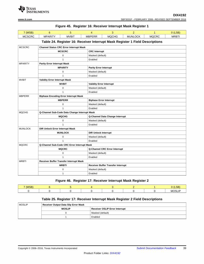
39
DIX4192www.ti.com SBFS031F –FEBRUARY 2006–REVISED SEPTEMBER 2016
Product Folder Links: DIX4192
Submit Documentation FeedbackCopyright © 2006–2016, Texas Instruments Incorporated
Figure 45. Register 16: Receiver Interrupt Mask Register 1
7 (MSB) 6 5 4 3 2 1 0 (LSB)MCSCRC MPARITY MVBIT MBPERR MQCHG MUNLOCK MQCRC MRBTI
Table 24. Register 16: Receiver Interrupt Mask Register 1 Field DescriptionsMCSCRC Channel Status CRC Error Interrupt Mask
MCSCRC CRC Interrupt
0 Masked (default)
1 Enabled
MPARITY Parity Error Interrupt Mask
MPARITY Parity Error Interrupt
0 Masked (default)
1 Enabled
MVBIT Validity Error Interrupt Mask
MVBIT Validity Error Interrupt
0 Masked (default)
1 Enabled
MBPERR Biphase Encoding Error Interrupt Mask
MBPERR Biphase Error Interrupt
0 Masked (default)
1 Enabled
MQCHG Q-Channel Sub-Code Data Change Interrupt Mask
MQCHG Q-Channel Data Change Interrupt
0 Masked (default)
1 Enabled
MUNLOCK DIR Unlock Error Interrupt Mask
MUNLOCK DIR Unlock Interrupt
0 Masked (default)
1 Enabled
MQCRC Q-Channel Sub-Code CRC Error Interrupt Mask
MQCRC Q-Channel CRC Error Interrupt
0 Masked (default)
1 Enabled
MRBTI Receiver Buffer Transfer Interrupt Mask
MRBTI Receiver Buffer Transfer Interrupt
0 Masked (default)
1 Enabled
Figure 46. Register 17: Receiver Interrupt Mask Register 2
7 (MSB) 6 5 4 3 2 1 0 (LSB)0 0 0 0 0 0 0 MOSLIP
Table 25. Register 17: Receiver Interrupt Mask Register 2 Field DescriptionsMOSLIP Receiver Output Data Slip Error Mask
MOSLIP Receiver OSLIP Error Interrupt
0 Masked (default)
1 Enabled

40
DIX4192SBFS031F –FEBRUARY 2006–REVISED SEPTEMBER 2016 www.ti.com
Product Folder Links: DIX4192
Submit Documentation Feedback Copyright © 2006–2016, Texas Instruments Incorporated
Figure 47. Register 18: Receiver Interrupt Mode Register 1
7 (MSB) 6 5 4 3 2 1 0 (LSB)QCHGM1 QCHGM0 UNLOCKM1 UNLOCKM0 QCRCM1 QCRCM0 RBTIM1 RBTIM0
Table 26. Register 18: Receiver Interrupt Mode Register 1 Field DescriptionsQCHGM[1:0] Q-Channel Sub-Code Data Change Interrupt Mode
QCHGM1 QCHGM0 Interrupt Active State
0 0 Rising edge active (default)
0 1 Falling edge active
1 0 Level active
1 1 Reserved
UNLOCKM[1:0] DIR Unlock Error Interrupt Mode
UNLOCKM1 UNLOCKM0 Interrupt Active State
0 0 Rising edge active (default)
0 1 Falling edge active
1 0 Level active
1 1 Reserved
QCRCM[1:0] Q-Channel Sub-Code CRC Error Interrupt Mode
QCRCM1 QCRCM0 Interrupt Active State
0 0 Rising edge active (default)
0 1 Falling edge active
1 0 Level active
1 1 Reserved
RBTIM[1:0] Receive Buffer Transfer Interrupt Mode
RBTIM1 RBTIM0 Interrupt Active State
0 0 Rising edge active (default)
0 1 Falling edge active
1 0 Level active
1 1 Reserved

41
DIX4192www.ti.com SBFS031F –FEBRUARY 2006–REVISED SEPTEMBER 2016
Product Folder Links: DIX4192
Submit Documentation FeedbackCopyright © 2006–2016, Texas Instruments Incorporated
Figure 48. Register 19: Receiver Interrupt Mode Register 2
7 (MSB) 6 5 4 3 2 1 0 (LSB)CSCRCM1 CSCRCM0 PARITYM1 PARITYM0 VBITM1 VBITM0 BPERRM1 BPERRM0
Table 27. Register 19: Receiver Interrupt Mode Register 2 Field DescriptionsCSCRCM[1:0] Channel Status CRC Error Interrupt Mode
CSCRCM1 CSCRCM0 Interrupt Active State
0 0 Rising edge active (default)
0 1 Falling edge active
1 0 Level active
1 1 Reserved
PARITYM[1:0] Parity Error Interrupt Mode
PARITYM1 PARITYM0 Interrupt Active State
0 0 Rising edge active (default)
0 1 Falling edge active
1 0 Level active
1 1 Reserved
VBITM[1:0] Validity Error Interrupt Mode
VBITM1 VBITM0 Interrupt Active State
0 0 Rising edge active (default)
0 1 Falling edge active
1 0 Level active
1 1 Reserved
BPERRM[1:0] Biphase Encoding Error Interrupt Mode
BPERRM1 BPERRM0 Interrupt Active State
0 0 Rising edge active (default)
0 1 Falling edge active
1 0 Level active
1 1 Reserved
Figure 49. Register 1A: Receiver Interrupt Mode Register 3
7 (MSB) 6 5 4 3 2 1 0 (LSB)0 0 0 0 0 0 OSLIPM1 OSLIPM0
Table 28. Register 1A: Receiver Interrupt Mode Register 3 Field DescriptionsOSLIPM[1:0] Receiver Output Data Slip Error Interrupt Mode
OSLIPM1 OSLIPM0 Interrupt Active State
0 0 Rising edge active (default)
0 1 Falling edge active
1 0 Level active
1 1 Reserved

42
DIX4192SBFS031F –FEBRUARY 2006–REVISED SEPTEMBER 2016 www.ti.com
Product Folder Links: DIX4192
Submit Documentation Feedback Copyright © 2006–2016, Texas Instruments Incorporated
Figure 50. Register 1B: General-Purpose Output 1 (GPO1) Control Register
7 (MSB) 6 5 4 3 2 1 0 (LSB)0 0 0 0 GPO13 GPO12 GPO11 GPO10
Table 29. Register 1B: General-Purpose Output 1 (GPO1) Control Register Field DescriptionsGPO[13:10] General-Purpose Output 1 (GPO1) Configuration
These bits are used to set the state or data source for the general-purpose digital output pin GPO1.
GPO13 GPO12 GPO11 GPO10 GPO1 Function
0 0 0 0 GPO1 is forced low (default)
0 0 0 1 GPO1 is forced high
0 0 1 0 Reserved
0 0 1 1 Transmitter interrupt, active low
0 1 0 0 Receiver interrupt, active low
0 1 0 1 Receiver 50/15-μs pre-emphasis, active low
0 1 1 0 Receiver non-audio data, active high
0 1 1 1 Receiver non-valid data, active high
1 0 0 0 Receiver channel status bit
1 0 0 1 Receiver user data bit
1 0 1 0 Receiver block start clock
1 0 1 1 Receiver COPY bit(0 = copyright asserted, 1 = copyright not asserted)
1 1 0 0 Receiver L-bit(0 = first generation or higher, 1 = original)
1 1 0 1 Receiver parity error, active high
1 1 1 0 Receiver internal sync clock
1 1 1 1 Transmitter internal sync clock
Figure 51. Register 1C: General-Purpose Output 2 (GPO2) Control Register
7 (MSB) 6 5 4 3 2 1 0 (LSB)0 0 0 0 GPO23 GPO22 GPO21 GPO20
Table 30. Register 1C: General-Purpose Output 2 (GPO2) Control Register Field DescriptionsGPO[23:20] General-Purpose Output 2 (GPO2) Configuration
These bits are used to set the state or data source for the general-purpose digital output pin GPO2.
GPO23 GPO22 GPO21 GPO20 GPO2 Function
0 0 0 0 GPO2 is forced low (default)
0 0 0 1 GPO2 is forced high
0 0 1 0 Reserved
0 0 1 1 Transmitter interrupt, active low
0 1 0 0 Receiver interrupt, active low
0 1 0 1 Receiver 50/15-μs pre-emphasis, active low
0 1 1 0 Receiver non-audio data, active high
0 1 1 1 Receiver non-valid data, active high
1 0 0 0 Receiver channel status bit
1 0 0 1 Receiver user data bit
1 0 1 0 Receiver block start clock
1 0 1 1 Receiver COPY bit(0 = copyright asserted, 1 = copyright not asserted)
1 1 0 0 Receiver L-bit(0 = first generation or higher, 1 = original)
1 1 0 1 Receiver parity error, active high
1 1 1 0 Receiver internal sync clock
1 1 1 1 Transmitter internal sync clock

43
DIX4192www.ti.com SBFS031F –FEBRUARY 2006–REVISED SEPTEMBER 2016
Product Folder Links: DIX4192
Submit Documentation FeedbackCopyright © 2006–2016, Texas Instruments Incorporated
Figure 52. Register 1D: General-Purpose Output 3 (GPO3) Control Register
7 (MSB) 6 5 4 3 2 1 0 (LSB)0 0 0 0 GPO33 GPO32 GPO31 GPO30
Table 31. Register 1D: General-Purpose Output 3 (GPO3) Control Register Field DescriptionsGPO[33:30] General-Purpose Output 3 (GPO3) Configuration
These bits are used to set the state or data source for the general-purpose digital output pin GPO3.
GPO33 GPO32 GPO31 GPO30 GPO3 Function
0 0 0 0 GPO3 is forced low (default)
0 0 0 1 GPO3 is forced high
0 0 1 0 Reserved
0 0 1 1 Transmitter interrupt, active low
0 1 0 0 Receiver interrupt, active low
0 1 0 1 Receiver 50/15-μs pre-emphasis, active low
0 1 1 0 Receiver non-audio data, active high
0 1 1 1 Receiver non-valid data, active high
1 0 0 0 Receiver channel status bit
1 0 0 1 Receiver user data bit
1 0 1 0 Receiver block start clock
1 0 1 1 Receiver COPY bit(0 = copyright asserted, 1 = copyright not asserted)
1 1 0 0 Receiver L-bit(0 = first generation or higher, 1 = original)
1 1 0 1 Receiver parity error, active high
1 1 1 0 Receiver internal sync clock
1 1 1 1 Transmitter internal sync clock
Figure 53. Register 1E: General-Purpose Output 4 (GPO4) Control Register
7 (MSB) 6 5 4 3 2 1 0 (LSB)0 0 0 0 GPO43 GPO42 GPO41 GPO40
Table 32. Register 1E: General-Purpose Output 4 (GPO4) Control Register Field DescriptionsGPO[43:40] General-Purpose Output 4 (GPO4) Configuration
These bits are used to set the state or data source for the general-purpose digital output pin GPO4.
GPO43 GPO42 GPO41 GPO40 GPO4 Function
0 0 0 0 GPO4 is forced low (default)
0 0 0 1 GPO4 is forced high
0 0 1 0 Reserved
0 0 1 1 Transmitter interrupt, active low
0 1 0 0 Receiver interrupt, active low
0 1 0 1 Receiver 50/15-μs pre-emphasis, active low
0 1 1 0 Receiver non-audio data, active high
0 1 1 1 Receiver non-valid data, active high
1 0 0 0 Receiver channel status bit
1 0 0 1 Receiver user data bit
1 0 1 0 Receiver block start clock
1 0 1 1 Receiver COPY bit(0 = copyright asserted, 1 = copyright not asserted)
1 1 0 0 Receiver L-bit(0 = first generation or higher, 1 = original)
1 1 0 1 Receiver parity error, active high
1 1 1 0 Receiver internal sync clock
1 1 1 1 Transmitter internal sync clock

44
DIX4192SBFS031F –FEBRUARY 2006–REVISED SEPTEMBER 2016 www.ti.com
Product Folder Links: DIX4192
Submit Documentation Feedback Copyright © 2006–2016, Texas Instruments Incorporated
9.5.2.1 Registers 1F through 28: Q-Channel Sub-Code Data RegistersRegisters 0x1F through 0x28 comprise the Q-channel sub-code buffer, which may be accessed for audio CDplayback. The Q-channel data provides information regarding the playback status for the current disc. The bufferdata is decoded by the DIR block.
Figure 54. Register 1F: Q-Channel Sub-Code Data Register 1 (Read-Only), Bits[7:0], Control and Address
7 (MSB) 6 5 4 3 2 1 0 (LSB)Q0 Q1 Q2 Q3 Q4 Q5 Q6 Q7
Figure 55. Register 20: Q-Channel Sub-Code Data Register 2 (Read-Only), Bits[15:8], Track
7 (MSB) 6 5 4 3 2 1 0 (LSB)Q8 Q9 Q10 Q11 Q12 Q13 Q14 Q15
Figure 56. Register 21: Q-Channel Sub-Code Data Register 3 (Read-Only), Bits[23:16], Index
7 (MSB) 6 5 4 3 2 1 0 (LSB)Q16 Q17 Q18 Q19 Q20 Q21 Q22 Q23
Figure 57. Register 22: Q-Channel Sub-Code Data Register 4 (Read-Only), Bits[31:24], Minutes
7 (MSB) 6 5 4 3 2 1 0 (LSB)Q24 Q25 Q26 Q27 Q28 Q29 Q30 Q31
Figure 58. Register 23: : Q-Channel Sub-Code Data Register 5 (Read-Only), Bits[39:32], Seconds
7 (MSB) 6 5 4 3 2 1 0 (LSB)Q32 Q33 Q34 Q35 Q36 Q37 Q38 Q39
Figure 59. Register 24: : Q-Channel Sub-Code Data Register 6 (Read-Only), Bits[47:40], Frame
7 (MSB) 6 5 4 3 2 1 0 (LSB)Q40 Q41 Q42 Q43 Q44 Q45 Q46 Q47
Figure 60. Register 25: Q-Channel Sub-Code Data Register 7 (Read-Only), Bits[55:48], Zero
7 (MSB) 6 5 4 3 2 1 0 (LSB)Q48 Q49 Q50 Q51 Q52 Q53 Q54 Q55
Figure 61. Register 26: Q-Channel Sub-Code Data Register 8 (Read-Only), Bits[63:56], AMIN
7 (MSB) 6 5 4 3 2 1 0 (LSB)Q56 Q57 Q58 Q59 Q60 Q61 Q62 Q63
Figure 62. Register 27: Q-Channel Sub-Code Data Register 9 (Read-Only), Bits[71:64], ASEC
7 (MSB) 6 5 4 3 2 1 0 (LSB)Q64 Q65 Q66 Q67 Q68 Q69 Q70 Q71
Figure 63. Register 28: Q-Channel Sub-Code Data Register 10 (Read-Only), Bits[79:72], AFRAME
7 (MSB) 6 5 4 3 2 1 0 (LSB)Q72 Q73 Q74 Q75 Q76 Q77 Q78 Q79

45
DIX4192www.ti.com SBFS031F –FEBRUARY 2006–REVISED SEPTEMBER 2016
Product Folder Links: DIX4192
Submit Documentation FeedbackCopyright © 2006–2016, Texas Instruments Incorporated
9.5.2.2 Registers 29 through 2C: IEC61937 PC/PD Burst PreambleThe PC and PD burst preambles are part of the IEC61937 standard for transmission of data reduced, non-PCMaudio over a standard two-channel interface (IEC60958). Examples of data-reduced formats include Dolby AC-3,DTS, various flavors of MPEG audio (including AAC), and Sony ATRAC. The PA and PB preambles providesynchronization data, and are fixed values of 0xF872 and 0x4E1F, respectively. The PC preamble indicates thetype of data being carried by the interface and the PD preamble indicates the length of the burst, given asnumber of bits.
Registers 0x29 through 0x2C contain the PC and PD preambles as decoded by the DIR block.
Figure 64. Register 29: Burst Preamble PC High-Byte Status Register (Read-Only)
7 (MSB) 6 5 4 3 2 1 0 (LSB)PC15 PC14 PC13 PC12 PC11 PC10 PC09 PC08
Figure 65. Register 2A: Burst Preamble PC Low-Byte Status Register (Read-Only)
7 (MSB) 6 5 4 3 2 1 0 (LSB)PC07 PC06 PC05 PC04 PC03 PC02 PC01 PC00
Table 33. Register 2A: Burst Preamble PC Low-Byte Status Register (Read-Only) Field DescriptionsPC[4:0], Hex Data Type
00 Null
01 Dolby AC-3
02 Reserved
03 Pause
04 MPEG-1 layer 1
05 MPEG-1 layer 2 or 3, or MPEG-2 without extension
06 MPEG-2 Data with extension
07 MPEG-2 AAC ADTS
08 MPEG-2 layer 1 low sample rate
09 MPEG-2 layer 2 or 3 low sample rate
0A Reserved
0B DTS type 1
0C DTS type 2
0D DTS type 3
0E ATRAC
0F ATRAC2/3
10-1F Reserved
Bits PC[6:5] are both set to 0.Bit PC[7] is an Error Flag, where: 0 = A valid burst-payload; 1 = Burst-payload may contain errors.Bits PC[12:8] are data-type dependent.Bits PC[15:13] indicate the stream number, which is set to 0.
Figure 66. Register 2B: Burst Preamble PD High-Byte Status Register (Read-Only)
7 (MSB) 6 5 4 3 2 1 0 (LSB)PD15 PD14 PD13 PD12 PD11 PD10 PD09 PD08
Figure 67. Register 2C: Burst Preamble PD Low-Byte Status Register (Read-Only)
7 (MSB) 6 5 4 3 2 1 0 (LSB)PD07 PD06 PD05 PD04 PD03 PD02 PD01 PD00

46
DIX4192SBFS031F –FEBRUARY 2006–REVISED SEPTEMBER 2016 www.ti.com
Product Folder Links: DIX4192
Submit Documentation Feedback Copyright © 2006–2016, Texas Instruments Incorporated
Figure 68. Register 7F: Page Selection Register
7 (MSB) 6 5 4 3 2 1 0 (LSB)0 0 0 0 0 0 PAGE1 PAGE0
Table 34. Register 7F: Page Selection Register Field DescriptionsPAGE[1:0] Page Selection
These bits are used to select one of three register pages for write and/or read access through the SPI or I2C serial host interface. ThePage Selection Register is present on every register page at address 0x7F, allowing movement between pages as necessary.
PAGE1 PAGE0 Register/Buffer Page Selection
0 0 Page 0, control and status registers (default)
0 1 Page 1, DIR channel status and user data buffers
1 0 Page 2, DIT channel status and user data buffers
1 1 Page 3, reserved
9.5.3 Channel Status and User Data Buffer MapsTable 35 through Table 38 show the buffer maps for the DIR and DIT channel status and user data buffers.
For Table 35, the channel status byte definitions are dependent on the transmission mode, either Professional orConsumer. Bit 0 of Byte 0 defines the transmission mode, 0 for Consumer mode, and 1 for Professional mode.This is applicable for Table 35 and Table 36.
For Table 37, the channel status byte definitions are dependent on the transmission mode, either Professional orConsumer. Bit 0 of Byte 0 defines the transmission mode, 0 for Consumer mode, and 1 for Professional mode. InProfessional mode, Byte 23 for each channel is reserved for CRC data, which is automatically calculated andencoded by the DIT. There is no requirement to program Byte 23 for either channel in Professional mode.

47
DIX4192www.ti.com SBFS031F –FEBRUARY 2006–REVISED SEPTEMBER 2016
Product Folder Links: DIX4192
Submit Documentation FeedbackCopyright © 2006–2016, Texas Instruments Incorporated
Table 35. DIR Channel Status Data Buffer Map (Register Page 1)ADDRESS
(Hex) CHANNEL BYTE BIT 0 (MSB) BIT 1 BIT 2 BIT 3 BIT 4 BIT 5 BIT 6 BIT 7
0 1 0 D0 D1 D2 D3 D4 D5 D6 D7
1 2 0 D0 D1 D2 D3 D4 D5 D6 D7
2 1 1 D0 D1 D2 D3 D4 D5 D6 D7
3 2 1 D0 D1 D2 D3 D4 D5 D6 D7
4 1 2 D0 D1 D2 D3 D4 D5 D6 D7
5 2 2 D0 D1 D2 D3 D4 D5 D6 D7
6 1 3 D0 D1 D2 D3 D4 D5 D6 D7
7 2 3 D0 D1 D2 D3 D4 D5 D6 D7
8 1 4 D0 D1 D2 D3 D4 D5 D6 D7
9 2 4 D0 D1 D2 D3 D4 D5 D6 D7
A 1 5 D0 D1 D2 D3 D4 D5 D6 D7
B 2 5 D0 D1 D2 D3 D4 D5 D6 D7
C 1 6 D0 D1 D2 D3 D4 D5 D6 D7
D 2 6 D0 D1 D2 D3 D4 D5 D6 D7
E 1 7 D0 D1 D2 D3 D4 D5 D6 D7
F 2 7 D0 D1 D2 D3 D4 D5 D6 D7
10 1 8 D0 D1 D2 D3 D4 D5 D6 D7
11 2 8 D0 D1 D2 D3 D4 D5 D6 D7
12 1 9 D0 D1 D2 D3 D4 D5 D6 D7
13 2 9 D0 D1 D2 D3 D4 D5 D6 D7
14 1 10 D0 D1 D2 D3 D4 D5 D6 D7
15 2 10 D0 D1 D2 D3 D4 D5 D6 D7
16 1 11 D0 D1 D2 D3 D4 D5 D6 D7
17 2 11 D0 D1 D2 D3 D4 D5 D6 D7
18 1 12 D0 D1 D2 D3 D4 D5 D6 D7
19 2 12 D0 D1 D2 D3 D4 D5 D6 D7
1A 1 13 D0 D1 D2 D3 D4 D5 D6 D7
1B 2 13 D0 D1 D2 D3 D4 D5 D6 D7
1C 1 14 D0 D1 D2 D3 D4 D5 D6 D7
1D 2 14 D0 D1 D2 D3 D4 D5 D6 D7
1E 1 15 D0 D1 D2 D3 D4 D5 D6 D7
1F 2 15 D0 D1 D2 D3 D4 D5 D6 D7
20 1 16 D0 D1 D2 D3 D4 D5 D6 D7
21 2 16 D0 D1 D2 D3 D4 D5 D6 D7
22 1 17 D0 D1 D2 D3 D4 D5 D6 D7
23 2 17 D0 D1 D2 D3 D4 D5 D6 D7
24 1 18 D0 D1 D2 D3 D4 D5 D6 D7
25 2 18 D0 D1 D2 D3 D4 D5 D6 D7
26 1 19 D0 D1 D2 D3 D4 D5 D6 D7
27 2 19 D0 D1 D2 D3 D4 D5 D6 D7
28 1 20 D0 D1 D2 D3 D4 D5 D6 D7
29 2 20 D0 D1 D2 D3 D4 D5 D6 D7
2A 1 21 D0 D1 D2 D3 D4 D5 D6 D7
2B 2 21 D0 D1 D2 D3 D4 D5 D6 D7
2C 1 22 D0 D1 D2 D3 D4 D5 D6 D7
2D 2 22 D0 D1 D2 D3 D4 D5 D6 D7
2E 1 23 D0 D1 D2 D3 D4 D5 D6 D7
2F 2 23 D0 D1 D2 D3 D4 D5 D6 D7

48
DIX4192SBFS031F –FEBRUARY 2006–REVISED SEPTEMBER 2016 www.ti.com
Product Folder Links: DIX4192
Submit Documentation Feedback Copyright © 2006–2016, Texas Instruments Incorporated
Table 36. DIR User Data Buffer Map (Register Page 1)ADDRESS
(Hex) CHANNEL BYTE BIT 0 (MSB) BIT 1 BIT 2 BIT 3 BIT 4 BIT 5 BIT 6 BIT 7
40 1 0 D0 D1 D2 D3 D4 D5 D6 D7
41 2 0 D0 D1 D2 D3 D4 D5 D6 D7
42 1 1 D0 D1 D2 D3 D4 D5 D6 D7
43 2 1 D0 D1 D2 D3 D4 D5 D6 D7
44 1 2 D0 D1 D2 D3 D4 D5 D6 D7
45 2 2 D0 D1 D2 D3 D4 D5 D6 D7
46 1 3 D0 D1 D2 D3 D4 D5 D6 D7
47 2 3 D0 D1 D2 D3 D4 D5 D6 D7
48 1 4 D0 D1 D2 D3 D4 D5 D6 D7
49 2 4 D0 D1 D2 D3 D4 D5 D6 D7
4A 1 5 D0 D1 D2 D3 D4 D5 D6 D7
4B 2 5 D0 D1 D2 D3 D4 D5 D6 D7
4C 1 6 D0 D1 D2 D3 D4 D5 D6 D7
4D 2 6 D0 D1 D2 D3 D4 D5 D6 D7
4E 1 7 D0 D1 D2 D3 D4 D5 D6 D7
4F 2 7 D0 D1 D2 D3 D4 D5 D6 D7
50 1 8 D0 D1 D2 D3 D4 D5 D6 D7
51 2 8 D0 D1 D2 D3 D4 D5 D6 D7
52 1 9 D0 D1 D2 D3 D4 D5 D6 D7
53 2 9 D0 D1 D2 D3 D4 D5 D6 D7
54 1 10 D0 D1 D2 D3 D4 D5 D6 D7
55 2 10 D0 D1 D2 D3 D4 D5 D6 D7
56 1 11 D0 D1 D2 D3 D4 D5 D6 D7
57 2 11 D0 D1 D2 D3 D4 D5 D6 D7
58 1 12 D0 D1 D2 D3 D4 D5 D6 D7
59 2 12 D0 D1 D2 D3 D4 D5 D6 D7
5A 1 13 D0 D1 D2 D3 D4 D5 D6 D7
5B 2 13 D0 D1 D2 D3 D4 D5 D6 D7
5C 1 14 D0 D1 D2 D3 D4 D5 D6 D7
5D 2 14 D0 D1 D2 D3 D4 D5 D6 D7
5E 1 15 D0 D1 D2 D3 D4 D5 D6 D7
5F 2 15 D0 D1 D2 D3 D4 D5 D6 D7
60 1 16 D0 D1 D2 D3 D4 D5 D6 D7
61 2 16 D0 D1 D2 D3 D4 D5 D6 D7
62 1 17 D0 D1 D2 D3 D4 D5 D6 D7
63 2 17 D0 D1 D2 D3 D4 D5 D6 D7
64 1 18 D0 D1 D2 D3 D4 D5 D6 D7
65 2 18 D0 D1 D2 D3 D4 D5 D6 D7
66 1 19 D0 D1 D2 D3 D4 D5 D6 D7
67 2 19 D0 D1 D2 D3 D4 D5 D6 D7
68 1 20 D0 D1 D2 D3 D4 D5 D6 D7
69 2 20 D0 D1 D2 D3 D4 D5 D6 D7
6A 1 21 D0 D1 D2 D3 D4 D5 D6 D7
6B 2 21 D0 D1 D2 D3 D4 D5 D6 D7
6C 1 22 D0 D1 D2 D3 D4 D5 D6 D7
6D 2 22 D0 D1 D2 D3 D4 D5 D6 D7
6E 1 23 D0 D1 D2 D3 D4 D5 D6 D7
6F 2 23 D0 D1 D2 D3 D4 D5 D6 D7

49
DIX4192www.ti.com SBFS031F –FEBRUARY 2006–REVISED SEPTEMBER 2016
Product Folder Links: DIX4192
Submit Documentation FeedbackCopyright © 2006–2016, Texas Instruments Incorporated
Table 37. DIT Channel Status Data Buffer Map (Register Page 2)ADDRESS
(Hex) CHANNEL BYTE BIT 0 (MSB) BIT 1 BIT 2 BIT 3 BIT 4 BIT 5 BIT 6 BIT 7
0 1 0 D0 D1 D2 D3 D4 D5 D6 D7
1 2 0 D0 D1 D2 D3 D4 D5 D6 D7
2 1 1 D0 D1 D2 D3 D4 D5 D6 D7
3 2 1 D0 D1 D2 D3 D4 D5 D6 D7
4 1 2 D0 D1 D2 D3 D4 D5 D6 D7
5 2 2 D0 D1 D2 D3 D4 D5 D6 D7
6 1 3 D0 D1 D2 D3 D4 D5 D6 D7
7 2 3 D0 D1 D2 D3 D4 D5 D6 D7
8 1 4 D0 D1 D2 D3 D4 D5 D6 D7
9 2 4 D0 D1 D2 D3 D4 D5 D6 D7
A 1 5 D0 D1 D2 D3 D4 D5 D6 D7
B 2 5 D0 D1 D2 D3 D4 D5 D6 D7
C 1 6 D0 D1 D2 D3 D4 D5 D6 D7
D 2 6 D0 D1 D2 D3 D4 D5 D6 D7
E 1 7 D0 D1 D2 D3 D4 D5 D6 D7
F 2 7 D0 D1 D2 D3 D4 D5 D6 D7
10 1 8 D0 D1 D2 D3 D4 D5 D6 D7
11 2 8 D0 D1 D2 D3 D4 D5 D6 D7
12 1 9 D0 D1 D2 D3 D4 D5 D6 D7
13 2 9 D0 D1 D2 D3 D4 D5 D6 D7
14 1 10 D0 D1 D2 D3 D4 D5 D6 D7
15 2 10 D0 D1 D2 D3 D4 D5 D6 D7
16 1 11 D0 D1 D2 D3 D4 D5 D6 D7
17 2 11 D0 D1 D2 D3 D4 D5 D6 D7
18 1 12 D0 D1 D2 D3 D4 D5 D6 D7
19 2 12 D0 D1 D2 D3 D4 D5 D6 D7
1A 1 13 D0 D1 D2 D3 D4 D5 D6 D7
1B 2 13 D0 D1 D2 D3 D4 D5 D6 D7
1C 1 14 D0 D1 D2 D3 D4 D5 D6 D7
1D 2 14 D0 D1 D2 D3 D4 D5 D6 D7
1E 1 15 D0 D1 D2 D3 D4 D5 D6 D7
1F 2 15 D0 D1 D2 D3 D4 D5 D6 D7
20 1 16 D0 D1 D2 D3 D4 D5 D6 D7
21 2 16 D0 D1 D2 D3 D4 D5 D6 D7
22 1 17 D0 D1 D2 D3 D4 D5 D6 D7
23 2 17 D0 D1 D2 D3 D4 D5 D6 D7
24 1 18 D0 D1 D2 D3 D4 D5 D6 D7
25 2 18 D0 D1 D2 D3 D4 D5 D6 D7
26 1 19 D0 D1 D2 D3 D4 D5 D6 D7
27 2 19 D0 D1 D2 D3 D4 D5 D6 D7
28 1 20 D0 D1 D2 D3 D4 D5 D6 D7
29 2 20 D0 D1 D2 D3 D4 D5 D6 D7
2A 1 21 D0 D1 D2 D3 D4 D5 D6 D7
2B 2 21 D0 D1 D2 D3 D4 D5 D6 D7
2C 1 22 D0 D1 D2 D3 D4 D5 D6 D7
2D 2 22 D0 D1 D2 D3 D4 D5 D6 D7
2E 1 23 D0 D1 D2 D3 D4 D5 D6 D7
2F 2 23 D0 D1 D2 D3 D4 D5 D6 D7

50
DIX4192SBFS031F –FEBRUARY 2006–REVISED SEPTEMBER 2016 www.ti.com
Product Folder Links: DIX4192
Submit Documentation Feedback Copyright © 2006–2016, Texas Instruments Incorporated
Table 38. DIT User Data Buffer Map (Register Page 2)ADDRESS
(Hex) CHANNEL BYTE BIT 0 (MSB) BIT 1 BIT 2 BIT 3 BIT 4 BIT 5 BIT 6 BIT 7
40 1 0 D0 D1 D2 D3 D4 D5 D6 D7
41 2 0 D0 D1 D2 D3 D4 D5 D6 D7
42 1 1 D0 D1 D2 D3 D4 D5 D6 D7
43 2 1 D0 D1 D2 D3 D4 D5 D6 D7
44 1 2 D0 D1 D2 D3 D4 D5 D6 D7
45 2 2 D0 D1 D2 D3 D4 D5 D6 D7
46 1 3 D0 D1 D2 D3 D4 D5 D6 D7
47 2 3 D0 D1 D2 D3 D4 D5 D6 D7
48 1 4 D0 D1 D2 D3 D4 D5 D6 D7
49 2 4 D0 D1 D2 D3 D4 D5 D6 D7
4A 1 5 D0 D1 D2 D3 D4 D5 D6 D7
4B 2 5 D0 D1 D2 D3 D4 D5 D6 D7
4C 1 6 D0 D1 D2 D3 D4 D5 D6 D7
4D 2 6 D0 D1 D2 D3 D4 D5 D6 D7
4E 1 7 D0 D1 D2 D3 D4 D5 D6 D7
4F 2 7 D0 D1 D2 D3 D4 D5 D6 D7
50 1 8 D0 D1 D2 D3 D4 D5 D6 D7
51 2 8 D0 D1 D2 D3 D4 D5 D6 D7
52 1 9 D0 D1 D2 D3 D4 D5 D6 D7
53 2 9 D0 D1 D2 D3 D4 D5 D6 D7
54 1 10 D0 D1 D2 D3 D4 D5 D6 D7
55 2 10 D0 D1 D2 D3 D4 D5 D6 D7
56 1 11 D0 D1 D2 D3 D4 D5 D6 D7
57 2 11 D0 D1 D2 D3 D4 D5 D6 D7
58 1 12 D0 D1 D2 D3 D4 D5 D6 D7
59 2 12 D0 D1 D2 D3 D4 D5 D6 D7
5A 1 13 D0 D1 D2 D3 D4 D5 D6 D7
5B 2 13 D0 D1 D2 D3 D4 D5 D6 D7
5C 1 14 D0 D1 D2 D3 D4 D5 D6 D7
5D 2 14 D0 D1 D2 D3 D4 D5 D6 D7
5E 1 15 D0 D1 D2 D3 D4 D5 D6 D7
5F 2 15 D0 D1 D2 D3 D4 D5 D6 D7
60 1 16 D0 D1 D2 D3 D4 D5 D6 D7
61 2 16 D0 D1 D2 D3 D4 D5 D6 D7
62 1 17 D0 D1 D2 D3 D4 D5 D6 D7
63 2 17 D0 D1 D2 D3 D4 D5 D6 D7
64 1 18 D0 D1 D2 D3 D4 D5 D6 D7
65 2 18 D0 D1 D2 D3 D4 D5 D6 D7
66 1 19 D0 D1 D2 D3 D4 D5 D6 D7
67 2 19 D0 D1 D2 D3 D4 D5 D6 D7
68 1 20 D0 D1 D2 D3 D4 D5 D6 D7
69 2 20 D0 D1 D2 D3 D4 D5 D6 D7
6A 1 21 D0 D1 D2 D3 D4 D5 D6 D7
6B 2 21 D0 D1 D2 D3 D4 D5 D6 D7
6C 1 22 D0 D1 D2 D3 D4 D5 D6 D7
6D 2 22 D0 D1 D2 D3 D4 D5 D6 D7
6E 1 23 D0 D1 D2 D3 D4 D5 D6 D7
6F 2 23 D0 D1 D2 D3 D4 D5 D6 D7

51
DIX4192www.ti.com SBFS031F –FEBRUARY 2006–REVISED SEPTEMBER 2016
Product Folder Links: DIX4192
Submit Documentation FeedbackCopyright © 2006–2016, Texas Instruments Incorporated
10 Application and Implementation
NOTEInformation in the following applications sections is not part of the TI componentspecification, and TI does not warrant its accuracy or completeness. TI’s customers areresponsible for determining suitability of components for their purposes. Customers shouldvalidate and test their design implementation to confirm system functionality.
10.1 Application Information
Typical application diagrams and power-supply connections are presented in this section to aid the customer inhardware designs employing the DIX4192 device.
Figure 69 shows typical application connections for the DIX4192 using an SPI host interface. The SPI host willtypically be a microcontroller, digital signal processor, or programmable logic device. In addition to providing theSPI bus master, the host may be used to process interrupt and flag outputs from the DIX4192. The audio serialports are connected to external digital audio devices, which may include data converters, digital signalprocessors, digital audio interface receivers or transmitters, or other logic devices. The DIR inputs and DIToutputs are connected to line, optical, or logic interfaces (see Receiver Input Interfacing and Transmitter OutputInterfacing). Master and DIR reference clock sources are also shown.
Figure 70 shows typical application connections for the DIX4192 using an I2C bus interface. The I2C bus masterwill typically be a microcontroller, digital signal processor, or programmable logic device. In addition to providingthe I2C bus master, the host may be used to process interrupt and flag outputs from the DIX4192. Pullupresistors are connected from SCL (pin 20) and SDA (pin 22) to the VIO supply rail. These resistors are requiredfor the open drain outputs of the I2C interface. All other connections to the DIX4192 are the same as the SPI hostcase discussed previously.
Figure 71 shows the recommended power-supply connections and bypassing for the DIX4192. In this case, it isassumed that the VIO, VDD33, and VCC supplies are powered from the same 3.3-V power source. The VDD18core supply is powered from a separate supply, or derived from the 3.3-V supply using a linear voltage regulator,as shown with the optional regulator circuitry of Figure 71.
The 0.1-μF bypass capacitors are surface-mount X7R ceramic, and must be located as close to the device aspossible. These capacitors must be connected directly between the supply and corresponding ground pins of theDIX4192. The ground pin is then connected directly to the ground plane of the printed circuit board (PCB). Thelarger value capacitors, shown connected in parallel to the 0.1-μF capacitors, are recommended. At a minimum,there must at least be footprints on the PCB for installation of these larger capacitors, so that experiments can berun with and without the capacitors installed, in order to determine the effect on the measured performance of theDIX4192. The larger value capacitors can be surface-mount X7R multilayer ceramic or tantalum chip.
The substrate ground, BGND (pin 44), must be connected by a PCB trace to AGND (pin 10). The AGND pin isthen connected directly to the ground plane. This connection helps to reduce noise in the DIR section of thedevice, aiding the overall jitter and noise tolerance for the receiver.
A series resistor is shown between the 3.3-V supply and VCC (pin 9) connection. This resistor combines with thebypass capacitors to create a simple RC filter to remove higher frequency components from the VCC supply. Theseries resistor must be a metal film type for best filtering characteristics. As a substitute for the resistor, a ferritebead can be used, although it may have to be physically large in order to contribute to the filtering.

373839404142434445464748
123456789
10
1112
363534333231302928272625
24232221201918171615
1413
BCKALR KACSDI ANSDOUTANCVIODGND3BGNDSDOUTBSDI BNLR KBCBCKB
RX +1RX -1RX +2RX -2RX +3RX -3RX +4RX -4VCCAGNDLOCKRX KOC
SYNCBLS
AESO TUVDD 33
TX+TX-
DGND2GP 4OGP 3OGP 2OGP 1OMCLK
RSTINT
SDAA1
SCL
A0CPM
VDD 81DGND1
NCNC
RX KIC
DIX4192IPFB
From Digital Inputs(Line, Optica , Logl ic)
To Digital Outputs(Line, Optical, Logic)
To Host or Exte nalr Logic
To Host or Exte nalr Logic
I C2
Ho ts
Controller
AudioI/O
Device
AudioI/O
Device
DIRRef Clock
MasterClock
DIR Recovered Clock
VIO
10kW 2.7kW
TieLO or HI
373839404142434445464748
123456789
10
1112
363534333231302928272625
24232221201918171615
1413
BCKALRCKASDINASDOUTANCVIODGND3BGNDSDOUTBSDINBLRCKBBCKB
RX1+RX1-
RX2+RX2-
RX3+RX3-
RX4+RX4-
VCCAGNDLOCKRXCKO
SYNCBLS
AESOUTVDD33
TX+TX-
DGND2GPO4GPO3GPO2GPO1MCLK
RSTINT
CDOUTCDIN
CCLKCS
CPMVDD18DGND1
NCNC
RXCKI
DIX4192IPFB
From Digita Inpul ts(Line, Optical, Logic)
To Digital Outputs(L ne,i O ca Lpti l, ogic)
To Host o Exter alr n Logic
To Host or xternalE Logic
SPI
Host
Controller
AudioI/O
Device
AudioI/O
Device
DIRRef Clock
MasterClock
DIR Recovered Clock
VIO
10kW
52
DIX4192SBFS031F –FEBRUARY 2006–REVISED SEPTEMBER 2016 www.ti.com
Product Folder Links: DIX4192
Submit Documentation Feedback Copyright © 2006–2016, Texas Instruments Incorporated
Application Information (continued)
Figure 69. Typical Application Diagram Using SPI Host Interface(See Figure 71 for Power-Supply Connections)
Figure 70. Typical Application Diagram Using I2C Host Interface(See Figure 71 for Power-Supply Connections)

0.1mF
10 Fm 0.1 Fm 10 Fm0.1 Fm
+3. V3
9
10 30
33
4243
44
10 Fm
R
+
+
+
+
Connect pin 44 to pin 10.
Pi 10n i then connes cted to
the ground pl n .a e
+3. V3
0.1 Fm 0 01 Fm. 2.2 Fm
TPS79318DB RV
DIX4192IPFB
Optional Regulator Circuit
1716
R may be set from 2 t ced b fe te bW y a rri eo 10 or replaW, ad.C may be set to 10 F d when using the opt onal rm egulator circuit., or not installe i
1 53 4
2
INEN
OUTNR
GND
+1.8V
C
0.1 Fm
53
DIX4192www.ti.com SBFS031F –FEBRUARY 2006–REVISED SEPTEMBER 2016
Product Folder Links: DIX4192
Submit Documentation FeedbackCopyright © 2006–2016, Texas Instruments Incorporated
Application Information (continued)
Figure 71. Recommended Power-Supply Connections
10.1.1 Digital Audio Transformer VendorsTransformers are shown in this data sheet for both receiver and transmitter balanced and unbalanced lineinterface implementations. For the Texas Instruments Pro Audio evaluation modules, transformers from ScientificConversion are used. In addition to Scientific Conversion, there are other vendors that offer transformer productsfor digital audio interface applications. Please refer to the following manufacturer websites for details regardingtheir products and services. Other transformer vendors may also be available by searching catalog and/orInternet resources.• Scientific Conversion: http://scientificonversion.com• Schott Corporation: http://schottcorp.com• Pulse Engineering: http://pulseeng.com
10.1.2 Receiver Input InterfacingThis section details the recommended interfaces for the DIX4192 line receiver inputs. Balanced and unbalancedline interfaces, in addition to optical receiver and external logic interfacing, are discussed.
For professional digital audio interfaces, 110-Ω balanced line interfaces are either required or preferred.Transformer coupling is commonly employed to provide isolation and to improve common-mode noise rejection.Figure 72 shows the recommended transformer-coupled balanced line receiver interface for the DIX4192. Thetransformer is specified for a 1:1 turn ratio, and must exhibit low inter-winding capacitance for best performance.Due to the DC bias on the line receiver inputs, 0.1-μF capacitors are used for AC-coupling the transformer to theline receiver inputs. On the line side of the transformer, an optional 0.1-μF capacitor is shown for cases where aDC bias may be applied at the transmitter side of the connection. The coupling capacitors must be surface-mountceramic chip type with an X7R or C0G dielectric.

VDD33
0.1 Fm
To RX+
To RX-
All-Plastic
(5 or 10 meters maximum)
(1) Toshiba TORX141 or equivalent.
Optical
Receiver(1)
(1) Insert a 0.1 F cap common-mode DCm acitor when blocking components.
1:1
75W
0.1 Fm
0.1 Fm
To RX+
To RX-
Dig tai l Input
75 UnbalanW ced
(RCA or BNC Connector)
C(1)
(a) Transformer-Coupled Unbalanced Line Interface
75W
0.1 Fm
0.1 Fm
To RX+
To RX-
Digital Input
75 UnbalanW ced
(RCA or BNC Connector)
(b) Unbalanced Line Interface Without Transformer
(1) Insert a 0.1 F cap common-mode DC voltage.m acitor when blocking
1:1
110W
0.1 Fm
0.1 Fm
To RX+
T Ro -X
3
2
1
XLR
Digital Input
110 BW alanced
C(1)
54
DIX4192SBFS031F –FEBRUARY 2006–REVISED SEPTEMBER 2016 www.ti.com
Product Folder Links: DIX4192
Submit Documentation Feedback Copyright © 2006–2016, Texas Instruments Incorporated
Application Information (continued)
Figure 72. Transformer-Coupled Balanced Input Interface
Unbalanced 75-Ω coaxial cable interfaces are commonly employed in consumer and broadcast audioapplications. Designs with and without transformer line coupling may be used. Figure 73(a) shows therecommended 75-Ω transformer-coupled line interface, which shares many similarities to the balanced designshown in Figure 72. Once again, the transformer provides isolation and improved noise rejection. Figure 73(b)shows the transformer-free interface, which is commonly used for S/PDIF consumer connections.
Figure 73. Unbalanced Line Input Interfaces
Optical interfaces using all-plastic fiber are commonly employed for consumer audio equipment whereinterconnections are less than 10 m in length. Optical receiver modules used for a digital audio interface operatefrom either a single 3.3-V or 5-V supply and have a TTL–, CMOS-, or low-voltage CMOS-compatible logic output.Interfacing to 3.3-V optical receivers is straightforward when the optical receiver supply is powered from theDIX4192 VDD33 power source, as shown in Figure 74. For the 5-V optical receivers, the output high logic levelmay exceed the DIX4192 line receiver absolute maximum input voltage. A level translator is required, placedbetween the optical receiver output and the DIX4192 line receiver input. Figure 75 shows the recommendedinput circuit when interfacing a 5-V optical receiver to the DIX4192 line receiver inputs. The Texas InstrumentsSN74LVC1G125 single buffer IC is operated from the same 3.3-V supply used for DIX4192 VDD33 supply. Thisbuffer includes a 5-V tolerant digital input, and provides the logic level translation required for the interface.
Figure 74. Interfacing to a 3.3-V Optical Receiver Module

SN74LVC1G125
or Equivalent
0.1mF
T RX+o
To RX-
From +5V Logic
(TTL or CMOS)
VDD33
5
2
31
4
SN74AVC1T45
or Equivalent
0.1mF
T RX+o
To RX-
From +1.8V or +2.5V
CMOS Logic
+1.8V or +2.5V
5VDD33
63
1
2
4
(1) Toshiba TORX173, TORX176, TORX179, or equivalent.
+5V
SN74LVC1G125
or Equivalent
0.1mF
T RX+o
To RX-
All-Plastic
(5 or 10 meters maximum)
Optical
Receiver(1)
VDD33
5
2
31
4
55
DIX4192www.ti.com SBFS031F –FEBRUARY 2006–REVISED SEPTEMBER 2016
Product Folder Links: DIX4192
Submit Documentation FeedbackCopyright © 2006–2016, Texas Instruments Incorporated
Application Information (continued)
Figure 75. Interfacing to a 5-V Optical Receiver Module
The DIX4192 line receivers may also be driven directly from external logic or line receiver devices with TTL orCMOS outputs. If the logic driving the line receiver is operated from 3.3 V, then logic level translation will not berequired. However, if the external logic is operated from a power-supply voltage that exceeds the maximumVDD33 supply voltage of the DIX4192, or operates from a supply voltage lower than 3.3 V, then level translationis required. Figure 76 shows the recommended logic level translation methods, using buffers and leveltranslators available from Texas Instruments.
Figure 76. CMOS and TTL Input Logic Interface
10.1.3 Transmitter Output InterfacingThis section details the recommended interfaces for the DIX4192 transmitter line driver and CMOS-bufferedoutputs. Balanced and unbalanced line interfaces, in addition to optical transmitter and external logic interfacing,will be discussed.
For professional digital audio interfaces, 110-Ω balanced line interfaces are either required or preferred.Transformer coupling is commonly employed to provide isolation and to improve common-mode noiseperformance. Figure 77 shows the recommended transformer-coupled balanced line driver interface for theDIX4192. The transformer is specified for a 1:1 turn ratio, and must exhibit low inter-winding capacitance for bestperformance. To eliminate residual DC bias, a 0.1-μF capacitor is used for AC-coupling the transformer to theline driver outputs. The coupling capacitor must be a surface-mount ceramic chip type with an X7R or C0Gdielectric.

R1 and R2 are selected to achieve the desired output voltage level while maintaining the required 75 transmitter output impedance.W
The TX+ output impedance is negligible.
(a) Transformer-Coupled Unbalanced Output
1:1
R2
0.1 Fm
TX+Digital Output
75 UnbalanW ced
(RCA or BNC connector)
R1
(b) Unbalanced Output Without Transformer
R2
0.1mF
TX+Digital Output
75 UnbalanW ced
(RCA or BNC connector)
R1
1:1
0.1 Fm
TX+
TX-
3
2
1
XLR
Digital Output
110 BW alanced
110W
56
DIX4192SBFS031F –FEBRUARY 2006–REVISED SEPTEMBER 2016 www.ti.com
Product Folder Links: DIX4192
Submit Documentation Feedback Copyright © 2006–2016, Texas Instruments Incorporated
Application Information (continued)
Figure 77. Transformer-Coupled Balanced Output Interface
Unbalanced 75-Ω coaxial cable interfaces are commonly employed in consumer and broadcast audioapplications. Designs with and without transformer line coupling may be used. Figure 78(a) shows therecommended 75-Ω transformer-coupled line driver interface, which shares many similarities to the balanceddesign shown in Figure 77. Figure 78(b) shows the transformer-free line driver interface, which is commonly usedfor S/PDIF consumer connections.
Figure 78. Unbalanced Line Output Interfaces
Optical interfaces using all-plastic fiber are commonly employed for consumer audio equipment whereinterconnections are less than 10 m in length. Most optical transmitter modules used for a digital audio interfaceoperate from a single 3.3-V or 5-V supply and have a TTL-compatible logic input. The CMOS-buffered transmitteroutput of the DIX4192, AESOUT (pin 34), is capable of driving the optical transmitter with VIO supply voltagesdown to 3 V. If the VIO supply voltage is less than 3 V, then level translation logic is required to drive the opticaltransmitter input. A good choice for this application is the Texas Instruments SN74AVC1T45 single bustransceiver. This device features two power-supply rails, one for the input side and one for the output side. Forthis application, the input side supply is powered from the VIO supply, while the output side is powered from a3.3-V supply. This configuration will boost the logic high level to a voltage suitable for driving the TTL-compatibleinput configuration. Figure 79 shows the recommended optical transmitter interface circuits.

SN74AVC1T45
or Equivalent
If VIO < +3.0V.
VIO
+5V
5
+3.3V
63
1
2
4
To Balanced or Unbalanced
Line InterfaceAESOUT
2
8
7
To Balanced or Unbalanced
Line Interface
3
6
5
1
1
SN75ALS191
SN74AHCT1G125
or Equivalent
+5V
5
2
13
4
Direct to external logic
operating from the VIO supply.AESOUT
To +5V Logic
(VIO supply = +3.0V to +3.3V)
(1) Toshiba TOTX141, TOTX173, TOTX176, TOTX179, or equivalent.
SN74AVC1T45
or Equivalent
If VIO < +3.0V.
VIO
5
+3.3V
63
1
2
4
All-Plastic Fiber
(5 or 10 meters maximum)AESOUT
Optical
Transmitter(1)
57
DIX4192www.ti.com SBFS031F –FEBRUARY 2006–REVISED SEPTEMBER 2016
Product Folder Links: DIX4192
Submit Documentation FeedbackCopyright © 2006–2016, Texas Instruments Incorporated
Application Information (continued)
Figure 79. Interfacing to an Optical Transmitter Module
The AESOUT output may also be used to drive external logic or line driver devices directly. Figure 80 shows therecommended logic interface techniques, including connections with and without level translation. Figure 81shows an external line driver interface using the Texas Instruments SN75ALS191 dual differential line driver. Ifthe VIO supply of the DIX4192 is set from 3 V to 3.3 V, no logic level translation will be required between theAESOUT output and the line driver input. If the VIO supply voltage is below this range, then the optional logiclevel translation logic of Figure 81 will be required. The SN75ALS191 dual line driver is especially useful inapplications where simultaneous 75-Ω and 110-Ω line interfaces are required.
Figure 80. CMOS or TTL Output Logic Interface
Figure 81. External Line Driver Interface

S/PDIFIN
DIX4192
DSPx4
S/PDIFOUT
PCM x1
GPO/INT
I2Cx1
PCM5242
PCM x1
TPA6120A2
58
DIX4192SBFS031F –FEBRUARY 2006–REVISED SEPTEMBER 2016 www.ti.com
Product Folder Links: DIX4192
Submit Documentation Feedback Copyright © 2006–2016, Texas Instruments Incorporated
10.2 Typical Application
Figure 82. DIX4192 Typical Application
10.2.1 Design RequirementsFor this design example, use the parameters listed in Table 39.
Table 39. Design ParametersDESIGN PARAMETER EXAMPLE VALUE
Audio input PCM x2, differential S and PDIF x4Audio output PCM x2, S and PDIF x4
Control Host 12CRXCKI or MCLK 24.576 MHz
10.2.2 Detailed Design Procedure
10.2.2.1 Differential Line Inputs and OutputThe DIX4192 has a total of 4 differential Line inputs and one Differential Line output. The 4 inputs are MUXed toone port for decoding and the audio data is sent to the internal bus of the device. The differential line output canchoose from either the AES3 encoder or directly from one of the RX inputs. The AES3 encoder can encodeeither of the serial ports or the DIR itself. User data and channel status data can be updated in registers.
10.2.2.2 Serial PortsThe DIX4192 has two serial ports which each support both input and output of PCM data. This allows a device toreceive data from one of the serial ports and then return audio to the DIX4192 to be routed to another output ofthe DIX4192. For example in this application the DSP can receive audio from the DIX4192 that was input to theDIX4192 over S/PDIF, then after processing the DSP can send audio back the DIX4192 over the same serialport. This processed audio can then be sent back out the S/PDIF transmit port of the DIX4192 or to thePCM5242 DAC on the other serial port.

2
0
-2
-4
-6
-8
-10
-12
-14
-16
-18
-20
100
101
102
103
Jitter Frequency (Hz)
104
105
106
Jitte
r A
ttenuation (
dB
)
Peak J
itte
r (U
I)
-10
-20
-30
-40
-50
-60
-70
-80
-90
-100
-110
-120
-130
-140
-150
20 100 1k
Sinusoidal Jitter Frequency (Hz)
10k 100k
TH
D+
N R
atio (
dB
)
5
2
1
500m
200m
100m
50m
20m
10m
5m
2m
1m
THD+N
Output Jitter Amplitude
Input Jitter Amplitude
59
DIX4192www.ti.com SBFS031F –FEBRUARY 2006–REVISED SEPTEMBER 2016
Product Folder Links: DIX4192
Submit Documentation FeedbackCopyright © 2006–2016, Texas Instruments Incorporated
10.2.3 Application Curves
Figure 83. DIR Jitter Attenuation Characteristics Figure 84. DIR Jitter Tolerance Plot
11 Power Supply RecommendationsThe DIX4192 requires a 1.8-V and 3.3-V nominal supply rails. At least one 3.3-V supply is required for VCC,VDD33. VIO can operate at 1.8 V or at 3.3 V. VDD18 requires a 1.8-V nominal supply rail. The decouplingcapacitors for the power supplies must be placed close to the device terminals.

10 F 0.1 F
Top Layer Ground Pour and
PowerPadTop Layer Signal Traces
Pad to top layer ground
pour
It is recommended to place a top layer ground
pour for shielding around PCM9211 and
connect to lower main PCB ground plane by
multiple vias
DIX4192
Series resistors
between 50 -100 Qv
PCM ports can reduce
reflections if necessary
1
2
3
4
5
6
7
8
9
10
11
12
13 14 15 16 17 18 19 20 21 22 23 24
25
26
27
28
29
30
31
32
33
34
35
36
373839404142434445464748
+1.
8V
0.1 F
10 µF
VIO
+3.
3V0.1 F 10 F
0.1 F
SYNC
BC
KA
BLS
AESO
UTVDD3
3
TX+
TX-
DGND2
GPO4
GPO3
GPO2
GPO1
MCLK
LRC
K
A
SD
IN A
SD
OU
TAN
C
VIO
DG
N
D3
BG
ND
SD
OU
T
BSD
IN B
LRC
K
B
BC
KB
RX1+
RX1-
RX2+
RX2-
RX3+
RX3-
RX4+
RX4-
VCC
AGND
LOCK
RXCKO
RX
CK
I
NC
NC
DG
ND
1
VD
D1
8
CP
M
CS
,A0
OC
LK,S
CL
CD
IN1
,
A1
CD
OU
T,
SD
A
INT
RS
T
Port B PCM
Input and Output
Differential
Line Inputs
Control Interface
GPO to
Host
10 F
+3.
3V
Port A PCM
Input and Output
VIO
INT pin must be pulled
up to VIO through 10k
Q]
10N
60
DIX4192SBFS031F –FEBRUARY 2006–REVISED SEPTEMBER 2016 www.ti.com
Product Folder Links: DIX4192
Submit Documentation Feedback Copyright © 2006–2016, Texas Instruments Incorporated
12 Layout
12.1 Layout GuidelinesTI recommends to use one ground plane for the DIX4192. While using one ground plane, it is best to ensure thatanalog and digital circuitry be sufficiently partitioned on the PCB so that analog and digital return currents do notcross.• Decoupling capacitors must be placed as close to power pins as possible (VCC, VDD33, VDD18, VIO).• Further guidelines can be found in Layout Example.
12.2 Layout Example
Figure 85. DIX4192 Board Layout

61
DIX4192www.ti.com SBFS031F –FEBRUARY 2006–REVISED SEPTEMBER 2016
Product Folder Links: DIX4192
Submit Documentation FeedbackCopyright © 2006–2016, Texas Instruments Incorporated
13 Device and Documentation Support
13.1 Device Support
13.1.1 Third-Party Products DisclaimerTI'S PUBLICATION OF INFORMATION REGARDING THIRD-PARTY PRODUCTS OR SERVICES DOES NOTCONSTITUTE AN ENDORSEMENT REGARDING THE SUITABILITY OF SUCH PRODUCTS OR SERVICESOR A WARRANTY, REPRESENTATION OR ENDORSEMENT OF SUCH PRODUCTS OR SERVICES, EITHERALONE OR IN COMBINATION WITH ANY TI PRODUCT OR SERVICE.
13.1.2 Development SupportFor developmental support, see the following:• AES web site: http://www.aes.org• IEC web site: http://www.iec.ch• ANSI web site: http://www.ansi.org• Japanese Electronics and Information Technologies Industries Association (JEITA) website:
http://www.jeita.or.jp/english• Philips we site: http://www.philips.com• Scientificonversion web site: http://www.scientificonversion.com• Schott Magnetics web site: http://www.schottcorp.com/• Pulse Electronics web site: http://www.pulseelectronics.com/
13.2 Documentation Support
13.2.1 Related DocumentationFor related documentation, see the following:• DIT4096 96-kHz Digital Audio Transmitter, SBOS225• DIT4192 192-kHz Digital Audio Transmitter, SBOS229• SRC4184 4-Channel, Asynchronous Sample Rate Converter, SBFS026• SRC419 x 192-kHz Stereo Asynchronous Sample-Rate Converters, SBFS022• SN74LVC1G125 Single Bus Buffer Gate With 3-State Output, SCES223• SN74AVC1T45 Single-Bit Dual-Supply Bus Transceiver With Configurable Voltage Translation and 3-State
Outputs, SCES530• SN75ALS191 Dual Differential Line Driver, SLLS032
13.3 Receiving Notification of Documentation UpdatesTo receive notification of documentation updates, navigate to the device product folder on ti.com. In the upperright corner, click on Alert me to register and receive a weekly digest of any product information that haschanged. For change details, review the revision history included in any revised document.
13.4 Community ResourcesThe following links connect to TI community resources. Linked contents are provided "AS IS" by the respectivecontributors. They do not constitute TI specifications and do not necessarily reflect TI's views; see TI's Terms ofUse.
TI E2E™ Online Community TI's Engineer-to-Engineer (E2E) Community. Created to foster collaborationamong engineers. At e2e.ti.com, you can ask questions, share knowledge, explore ideas and helpsolve problems with fellow engineers.
Design Support TI's Design Support Quickly find helpful E2E forums along with design support tools andcontact information for technical support.
13.5 TrademarksE2E is a trademark of Texas Instruments.

62
DIX4192SBFS031F –FEBRUARY 2006–REVISED SEPTEMBER 2016 www.ti.com
Product Folder Links: DIX4192
Submit Documentation Feedback Copyright © 2006–2016, Texas Instruments Incorporated
13.5 Trademarks (continued)Dolby is a registered trademark of Dolby Laboratories, Inc.SPI is a trademark of Motorola.I2S is a trademark of NXP Semiconductors.All other trademarks are the property of their respective owners.
13.6 Electrostatic Discharge CautionThese devices have limited built-in ESD protection. The leads should be shorted together or the device placed in conductive foamduring storage or handling to prevent electrostatic damage to the MOS gates.
13.7 GlossarySLYZ022 — TI Glossary.
This glossary lists and explains terms, acronyms, and definitions.
14 Mechanical, Packaging, and Orderable InformationThe following pages include mechanical, packaging, and orderable information. This information is the mostcurrent data available for the designated devices. This data is subject to change without notice and revision ofthis document. For browser-based versions of this data sheet, refer to the left-hand navigation.

PACKAGE OPTION ADDENDUM
www.ti.com 7-Sep-2016
Addendum-Page 1
PACKAGING INFORMATION
Orderable Device Status(1)
Package Type PackageDrawing
Pins PackageQty
Eco Plan(2)
Lead/Ball Finish(6)
MSL Peak Temp(3)
Op Temp (°C) Device Marking(4/5)
Samples
DIX4192IPFB ACTIVE TQFP PFB 48 250 Green (RoHS& no Sb/Br)
CU NIPDAU Level-2-260C-1 YEAR -40 to 85 DIX4192I
DIX4192IPFBG4 ACTIVE TQFP PFB 48 250 Green (RoHS& no Sb/Br)
CU NIPDAU Level-2-260C-1 YEAR -40 to 85 DIX4192I
DIX4192IPFBR ACTIVE TQFP PFB 48 1000 Green (RoHS& no Sb/Br)
CU NIPDAU Level-2-260C-1 YEAR -40 to 85 DIX4192I
DIX4192IPFBRG4 ACTIVE TQFP PFB 48 1000 Green (RoHS& no Sb/Br)
CU NIPDAU Level-2-260C-1 YEAR -40 to 85 DIX4192I
(1) The marketing status values are defined as follows:ACTIVE: Product device recommended for new designs.LIFEBUY: TI has announced that the device will be discontinued, and a lifetime-buy period is in effect.NRND: Not recommended for new designs. Device is in production to support existing customers, but TI does not recommend using this part in a new design.PREVIEW: Device has been announced but is not in production. Samples may or may not be available.OBSOLETE: TI has discontinued the production of the device.
(2) Eco Plan - The planned eco-friendly classification: Pb-Free (RoHS), Pb-Free (RoHS Exempt), or Green (RoHS & no Sb/Br) - please check http://www.ti.com/productcontent for the latest availabilityinformation and additional product content details.TBD: The Pb-Free/Green conversion plan has not been defined.Pb-Free (RoHS): TI's terms "Lead-Free" or "Pb-Free" mean semiconductor products that are compatible with the current RoHS requirements for all 6 substances, including the requirement thatlead not exceed 0.1% by weight in homogeneous materials. Where designed to be soldered at high temperatures, TI Pb-Free products are suitable for use in specified lead-free processes.Pb-Free (RoHS Exempt): This component has a RoHS exemption for either 1) lead-based flip-chip solder bumps used between the die and package, or 2) lead-based die adhesive used betweenthe die and leadframe. The component is otherwise considered Pb-Free (RoHS compatible) as defined above.Green (RoHS & no Sb/Br): TI defines "Green" to mean Pb-Free (RoHS compatible), and free of Bromine (Br) and Antimony (Sb) based flame retardants (Br or Sb do not exceed 0.1% by weightin homogeneous material)
(3) MSL, Peak Temp. - The Moisture Sensitivity Level rating according to the JEDEC industry standard classifications, and peak solder temperature.
(4) There may be additional marking, which relates to the logo, the lot trace code information, or the environmental category on the device.
(5) Multiple Device Markings will be inside parentheses. Only one Device Marking contained in parentheses and separated by a "~" will appear on a device. If a line is indented then it is a continuationof the previous line and the two combined represent the entire Device Marking for that device.
(6) Lead/Ball Finish - Orderable Devices may have multiple material finish options. Finish options are separated by a vertical ruled line. Lead/Ball Finish values may wrap to two lines if the finishvalue exceeds the maximum column width.

PACKAGE OPTION ADDENDUM
www.ti.com 7-Sep-2016
Addendum-Page 2
Important Information and Disclaimer:The information provided on this page represents TI's knowledge and belief as of the date that it is provided. TI bases its knowledge and belief on informationprovided by third parties, and makes no representation or warranty as to the accuracy of such information. Efforts are underway to better integrate information from third parties. TI has taken andcontinues to take reasonable steps to provide representative and accurate information but may not have conducted destructive testing or chemical analysis on incoming materials and chemicals.TI and TI suppliers consider certain information to be proprietary, and thus CAS numbers and other limited information may not be available for release.
In no event shall TI's liability arising out of such information exceed the total purchase price of the TI part(s) at issue in this document sold by TI to Customer on an annual basis.
OTHER QUALIFIED VERSIONS OF DIX4192 :
• Automotive: DIX4192-Q1
NOTE: Qualified Version Definitions:
• Automotive - Q100 devices qualified for high-reliability automotive applications targeting zero defects

TAPE AND REEL INFORMATION
*All dimensions are nominal
Device PackageType
PackageDrawing
Pins SPQ ReelDiameter
(mm)
ReelWidth
W1 (mm)
A0(mm)
B0(mm)
K0(mm)
P1(mm)
W(mm)
Pin1Quadrant
DIX4192IPFBR TQFP PFB 48 1000 330.0 16.4 9.6 9.6 1.5 12.0 16.0 Q2
PACKAGE MATERIALS INFORMATION
www.ti.com 7-Sep-2016
Pack Materials-Page 1

*All dimensions are nominal
Device Package Type Package Drawing Pins SPQ Length (mm) Width (mm) Height (mm)
DIX4192IPFBR TQFP PFB 48 1000 367.0 367.0 38.0
PACKAGE MATERIALS INFORMATION
www.ti.com 7-Sep-2016
Pack Materials-Page 2

MECHANICAL DATA
MTQF019A – JANUARY 1995 – REVISED JANUARY 1998
POST OFFICE BOX 655303 • DALLAS, TEXAS 75265
PFB (S-PQFP-G48) PLASTIC QUAD FLATPACK
4073176/B 10/96
Gage Plane
0,13 NOM
0,25
0,450,75
Seating Plane
0,05 MIN
0,170,27
24
25
13
12
SQ
36
37
7,206,80
48
1
5,50 TYP
SQ8,809,20
1,050,95
1,20 MAX0,08
0,50 M0,08
0°–7°
NOTES: A. All linear dimensions are in millimeters.B. This drawing is subject to change without notice.C. Falls within JEDEC MS-026


IMPORTANT NOTICE
Texas Instruments Incorporated and its subsidiaries (TI) reserve the right to make corrections, enhancements, improvements and otherchanges to its semiconductor products and services per JESD46, latest issue, and to discontinue any product or service per JESD48, latestissue. Buyers should obtain the latest relevant information before placing orders and should verify that such information is current andcomplete. All semiconductor products (also referred to herein as “components”) are sold subject to TI’s terms and conditions of salesupplied at the time of order acknowledgment.TI warrants performance of its components to the specifications applicable at the time of sale, in accordance with the warranty in TI’s termsand conditions of sale of semiconductor products. Testing and other quality control techniques are used to the extent TI deems necessaryto support this warranty. Except where mandated by applicable law, testing of all parameters of each component is not necessarilyperformed.TI assumes no liability for applications assistance or the design of Buyers’ products. Buyers are responsible for their products andapplications using TI components. To minimize the risks associated with Buyers’ products and applications, Buyers should provideadequate design and operating safeguards.TI does not warrant or represent that any license, either express or implied, is granted under any patent right, copyright, mask work right, orother intellectual property right relating to any combination, machine, or process in which TI components or services are used. Informationpublished by TI regarding third-party products or services does not constitute a license to use such products or services or a warranty orendorsement thereof. Use of such information may require a license from a third party under the patents or other intellectual property of thethird party, or a license from TI under the patents or other intellectual property of TI.Reproduction of significant portions of TI information in TI data books or data sheets is permissible only if reproduction is without alterationand is accompanied by all associated warranties, conditions, limitations, and notices. TI is not responsible or liable for such altereddocumentation. Information of third parties may be subject to additional restrictions.Resale of TI components or services with statements different from or beyond the parameters stated by TI for that component or servicevoids all express and any implied warranties for the associated TI component or service and is an unfair and deceptive business practice.TI is not responsible or liable for any such statements.Buyer acknowledges and agrees that it is solely responsible for compliance with all legal, regulatory and safety-related requirementsconcerning its products, and any use of TI components in its applications, notwithstanding any applications-related information or supportthat may be provided by TI. Buyer represents and agrees that it has all the necessary expertise to create and implement safeguards whichanticipate dangerous consequences of failures, monitor failures and their consequences, lessen the likelihood of failures that might causeharm and take appropriate remedial actions. Buyer will fully indemnify TI and its representatives against any damages arising out of the useof any TI components in safety-critical applications.In some cases, TI components may be promoted specifically to facilitate safety-related applications. With such components, TI’s goal is tohelp enable customers to design and create their own end-product solutions that meet applicable functional safety standards andrequirements. Nonetheless, such components are subject to these terms.No TI components are authorized for use in FDA Class III (or similar life-critical medical equipment) unless authorized officers of the partieshave executed a special agreement specifically governing such use.Only those TI components which TI has specifically designated as military grade or “enhanced plastic” are designed and intended for use inmilitary/aerospace applications or environments. Buyer acknowledges and agrees that any military or aerospace use of TI componentswhich have not been so designated is solely at the Buyer's risk, and that Buyer is solely responsible for compliance with all legal andregulatory requirements in connection with such use.TI has specifically designated certain components as meeting ISO/TS16949 requirements, mainly for automotive use. In any case of use ofnon-designated products, TI will not be responsible for any failure to meet ISO/TS16949.
Products ApplicationsAudio www.ti.com/audio Automotive and Transportation www.ti.com/automotiveAmplifiers amplifier.ti.com Communications and Telecom www.ti.com/communicationsData Converters dataconverter.ti.com Computers and Peripherals www.ti.com/computersDLP® Products www.dlp.com Consumer Electronics www.ti.com/consumer-appsDSP dsp.ti.com Energy and Lighting www.ti.com/energyClocks and Timers www.ti.com/clocks Industrial www.ti.com/industrialInterface interface.ti.com Medical www.ti.com/medicalLogic logic.ti.com Security www.ti.com/securityPower Mgmt power.ti.com Space, Avionics and Defense www.ti.com/space-avionics-defenseMicrocontrollers microcontroller.ti.com Video and Imaging www.ti.com/videoRFID www.ti-rfid.comOMAP Applications Processors www.ti.com/omap TI E2E Community e2e.ti.comWireless Connectivity www.ti.com/wirelessconnectivity
Mailing Address: Texas Instruments, Post Office Box 655303, Dallas, Texas 75265Copyright © 2016, Texas Instruments Incorporated