inductor optimization procedure for power supply in … · · 2015-06-17are discussed in order to...
TRANSCRIPT

© 2011 IEEE
Proceedings of the IEEE Energy Conversion Congress and Exposition (ECCE USA 2011), Phoenix, USA, September 18-22, 2011.
Inductor Optimization Procedure for Power Supply in Package and Power Supply on Chip
T. AndersenC. ZingerliF. KrismerC. O‘MathunaJ.W. Kolar
This material is posted here with permission of the IEEE. Such permission of the IEEE does not in any way imply IEEE endorsement of any of ETH Zurich‘s products or services. Internal or personal use of this material is permitted. However, permission to reprint/republish this material for advertising or promotional purposes or for creating new collective works for resale or redistribution must be obtained from the IEEE by writing to [email protected]. By choosing to view this document, you agree to all provisions of the copyright laws protecting it.

Inductor Optimization Procedure for Power Supply
in Package and Power Supply on Chip
Toke M. Andersen, Claudius M. Zingerli,
Florian Krismer, and Johann W. Kolar
Power Electronic Systems Laboratory, ETH Zurich,
Zurich, Switzerland
Cian O’Mathuna
Tyndall National Institute, University College,
Cork, Ireland
Abstract—For Voltage Regulator Modules (VRM), integratingthe power converter with the load in an advanced integrationprocess is a method to deliver power at higher voltage levels,and thereby overcome the high supply current requirementspredicted by the 2009 International Technology Roadmap forSemiconductors (ITRS). The most conventional converter typeused is the buck or step-down converter. For this converter,the output inductor is recognized as the performance limitingcomponent with respect to efficiency and area requirements.This paper details an inductor optimization procedure for PowerSupply in Package (PSiP) and Power Supply on Chip (PwrSoC)applications. Targeting the highest possible efficiency for aspecified area-related power density, the optimization proceduredetermines the best inductor dimensions given the buck converteroperating conditions. The optimization procedure is verified usingexperimental data obtained from a PCB inductor realization.According to the results, the most favorable inductor achievesan efficiency of 94.5% and an area-related power density of1.97W/mm
2 at a switching frequency of 170MHz.
I. INTRODUCTION
From the 2009 International Technology Roadmap for
Semiconductors (ITRS) [1], the supply voltage of deep sub-
micron integrated circuits is expected to decrease from around
1.0V in 2009 to around 0.6V in 2025. However, the power
density is expected to remain almost constant during that
period, indicating an increase in supply current requirements.
Power delivery at low voltage and high current by an external
Point Of Load (POL) converter is troublesome since path
inductances and resistances cause supply instability and power
loss, respectively, and the required number of Controlled
Collapse Chip Connections (C4) for power delivery to the
chip increases [2]. An increased external supply voltage of
kVDD and an internal k:1 POL converter with an efficiency of
ηPOL facilitates a reduction of the supply current by a factor
of kηPOL for a desired power delivery to the on-chip load,
e.g. a microprocessor.
We distinguish between two types of power supply inte-
gration: Power Supply in Package (PSiP) and Power Supply
on Chip (PwrSoC) [3]. For PSiP, separate chips containing
switches, drivers, controllers, etc. are within the same package
but with external passives. For PwrSoC, a single chip contains
the switches, drivers, controllers, etc. and the passives are
integrated. Possibly, PwrSoC can be implemented on the same
die as the load.
65
70
75
80
85
90
95
100
[2], 2:1
[7], 2.4:1.5
[11], 4.2:3.3
[8], 1.2:0.9
Thermal limit
Pl =
1 W
/mm
2
Pl =
2 W
/mm
2
Linear 1.5:1
0.01 0.1 1 10
η / %
α / (W/mm2)
Ind. ext.SC Ind. int.
Fig. 1. Efficiency, η, vs. area-related power density, α, of published integratedpower converters. Each citet converter represents one specific design operatedat various load levels. The shown efficiency is the total converter efficiency,and the depicted power density is scaled with respect to the surface areaof the main energy storage component, i.e. the power inductor for inductorbased converters and the capacitors for switched capacitor converters. Theappertaining conversion ratio is given next to the citation.
Circuit topologies suited for PSiP and PwrSoC conver-
sion can be categorized as linear regulators, inductor based
converters, and switched capacitor (SC) converters. Linear
regulators, also known as Low Drop-Out (LDO) regulators,
are found impractical since their theoretically achievable effi-
ciency equals the conversion ratio; e.g. a 1.5:1 linear regula-
tor has a theoretical efficiency limit of 67%. The switched
capacitor approach has lately shown promising results for
fixed operating conditions, but it still lacks good regulation
capabilities such as regulation of load and line variations [2, 4].
The inductor based buck-type converter, shown in Fig. 2,
is a widely known converter topology with high regulation
capabilities, and it is considered an enabling technology for
PSiP and PwrSoC applications [5, 6].
Fig. 1 shows the efficiencies of published integrated power
converters and the area-related power densities of the main
energy storage component of the related converters,1 i.e. the
capacitors of a SC converter or the inductor of a buck
converter. Very high power densities are achieved with the
SC converter (ηmax = 90%) and for the buck converter with
1Ind. int.: buck converter with integrated inductor; Ind. ext.: buck converterwith external inductor.
978-1-4577-0541-0/11/$26.00 ©2011 IEEE 1320

+
−
−
+
L
Iin
Vin
Vout
Cout
Iout
iL(t)
Q1
Q2
Fig. 2. Classical buck converter implemented with two switches Q1 andQ2 driven in antiphase with duty cycle D. The output filter consists of theinductor L and the capacitor C which set the output current ripple and theoutput voltage ripple, respectively.
external inductors (ηmax = 84%) [2, 7], whereas the power
density and efficiency achieved with internal inductors are
considerably lower (α < 1.2W/mm2; ηmax = 77.9%) [8].
The 1.5:1 linear regulated is also shown in Fig. 1. The limit
in power density is determined by a thermal limit, which is
depicted as black lines.
The switches Q1 and Q2 in the buck converter shown
in Fig. 2 need to withstand the input voltage. The output
capacitance is determined from voltage ripple requirements,
and it may be reduced by using an interleaved design [6].
The inductor of an integrated buck converter is the most chal-
lenging component to design since inductors consume a large
amount of total converter area and have high losses compared
to discrete inductors. This results in low converter power
density and efficiency [9, 10]. Furthermore, the inductance
of integrated inductors is low compared to discrete inductors,
and therefore the switching frequency is chosen to be high to
accommodate the low inductance requirements [6, 9].
In this paper, we distinguish between three types of inductor
integration: on-chip inductors, on-top-of-chip inductors, and
Printed Circuit Board (PCB) inductors. For on-chip inductors,
the inductor is implemented using metal layers available in
the semiconductor manufacturing foundry. For on-top-of-chip
inductors, the inductor is fabricated on top of the silicon die
in a post-processing manufacturing step. For PCB inductors,
the inductor is external to the chip die. Both on-chip and on-
top-of-chip inductors are considered PwrSoC implementations
whereas the PCB inductor is considered a PSiP implementa-
tion [3]. For inductors in PwrSoC applications, the stray field
generated by the inductor can cause eddy currents in the silicon
substrate giving rise to substrate losses. A solution to this
problem is the patterned ground shield, which reduces this
effect on behalf of a slightly increased parasitic capacitance
to the substrate [12].
Investigated inductor geometries are the spiral and racetrack
inductors. The spiral inductor is readily available in most
semiconductor manufacturing processes. The racetrack induc-
tor has been used and studied in the literature, especially with
magnetic materials [5] or as a coupled inductor for a tapped
inductor buck converter [13]. In this paper, only coreless
inductors are considered since adding magnetic materials in
an integrated circuit foundry requires additional specialized
manufacturing steps [10]. A third inductor geometry, the toroid
inductor, which is often used in discrete buck converters,
becomes impractical for PSiP and PwrSoC because of its
three-dimensional structure.
The subject of this paper is an inductor optimization
procedure for designing inductors with the lowest possible
power loss for a desired inductor surface area. The output
of the procedure is the so-called α− η Pareto front [14],
which represents the set of inductors characterized by their
geometry parameters that give the best performance with
respect to both α and η. The proposed inductor optimization
procedure applies equally for PSiP and PwrSoC applications.
Experimental evaluation of practical inductors to verify the
procedure are performed on a macroscopic level owing to the
simpler manufacturing process of PCBs. Manufacturing on-
chip and on-top-of-chip inductors to verify the procedure will
be the subject of future research.
In Section II, the operating modes of the buck converter
are discussed in order to determine the inductance value
needed for a desired inductor current waveform and con-
verter switching frequency. Section III details the geometrical
models for spiral and racetrack inductors. A Finite Element
Method (FEM) simulator uses these geometrical models to
calculate the inductor parameters: inductance, dc resistance,
and ac resistance. The optimization procedure is presented
in Section IV and it utilizes the results obtained from the
FEM simulation to determine the α − η Pareto front. The
Pareto fronts of two case studies are presented and discussed
in section V. Based on these results, the most promising in-
ductor realizations are selected and manufactured on PCB for
verification of the proposed inductor optimization procedure.
Section VI concludes the paper.
II. BUCK CONVERTER OPERATION
The output voltage of the classical buck converter shown
in Fig. 2 is Vout = DVin, where D is the duty cycle and Vin
is the input voltage. The inductance L for a given peak-peak
inductor current ripple ∆ILpp is
L = Vout1−D
fsw∆ILpp, (1)
where fsw is the switching frequency. We define the Peak to
Average Ratio PAR of the inductor current as
PAR =ILp
Iout= 1 +
∆ILpp
2Iout, (2)
where ILp is the peak inductor current and Iout is the dc output
current. It can be shown that for 1 < PAR < 2, the buck
converter of Fig. 2 operates in Continuous Conduction Mode
(CCM1) with solely positive inductor currents iL(t) > 0,
for PAR > 2 in Continuous Conduction Mode (CCM2) with
positive and negative inductor currents, and for PAR = 2 in
Boundary Conduction Mode (BCM) with iL(t) ≥ 0.
It follows from (1) and (2) that the inductance L, the
inductor rms current IL(rms), and the peak energy WLp stored
1321
CCM1 CCM2
PAR = ILp / Iout
15
10
5
01 1.5 2 2.5 3 3.5 4
WLp
L
WLp / nJ
L / nH
2.5
2.0
1.5
1.01 1.5 2 2.5 3 3.5 4
IL(rms) /A
IL(rms)
PAR = ILp / Iout
CCM1 CCM2
Fig. 3. Inductance and peak energy stored in the inductor of a buck converterplotted against PAR (left); inductor rms current, IL(rms), plotted againstPAR (right). The selected operating conditions of the buck converter is:Vin = 1.6V, Vout = 0.8V, Iout = 1.25A, and fsw = 50MHz.
in the inductor can be expressed in terms of PAR as
L =Vin − Vout
2fswIout(PAR− 1)
Vout
Vin, (3)
IL(rms) =
√
I2out
(
1 +1
3(PAR− 1)2
)
, and (4)
WLp =1
2LI2Lp =
VoutIout4fsw
(
1−Vout
Vin
)
PAR2
PAR− 1, (5)
respectively. For the IL(rms) calculation, the inductor current
waveform is assumed to be triangular.
From Fig. 3, we see that the inductance decreases with
PAR, the rms inductor current increases with PAR, and that
the energy stored in the inductor is minimum in BCM when
PAR = 2. It is not straight forward to determine the best PARvalue based on these observations. Designing for CCM1, the
inductance and the energy storage requirement are high and
this yields a relatively large inductor resulting in a low power
density. Designing for CCM2, the inductance is low, however,
because of high peak currents, the peak stored energy is larger
than for BCM. Furthermore, high rms and peak currents in
the semiconductor switches Q1 and Q2 result in increased
conduction and switching losses of the transistors, thereby
reducing efficiency. Overall ripple for the design of the output
capacitor can be reduced by interleaving several stages. Thus,
BCM is typically considered a good design starting point as
a trade-off between efficiency and power density.
III. INDUCTOR MODELING
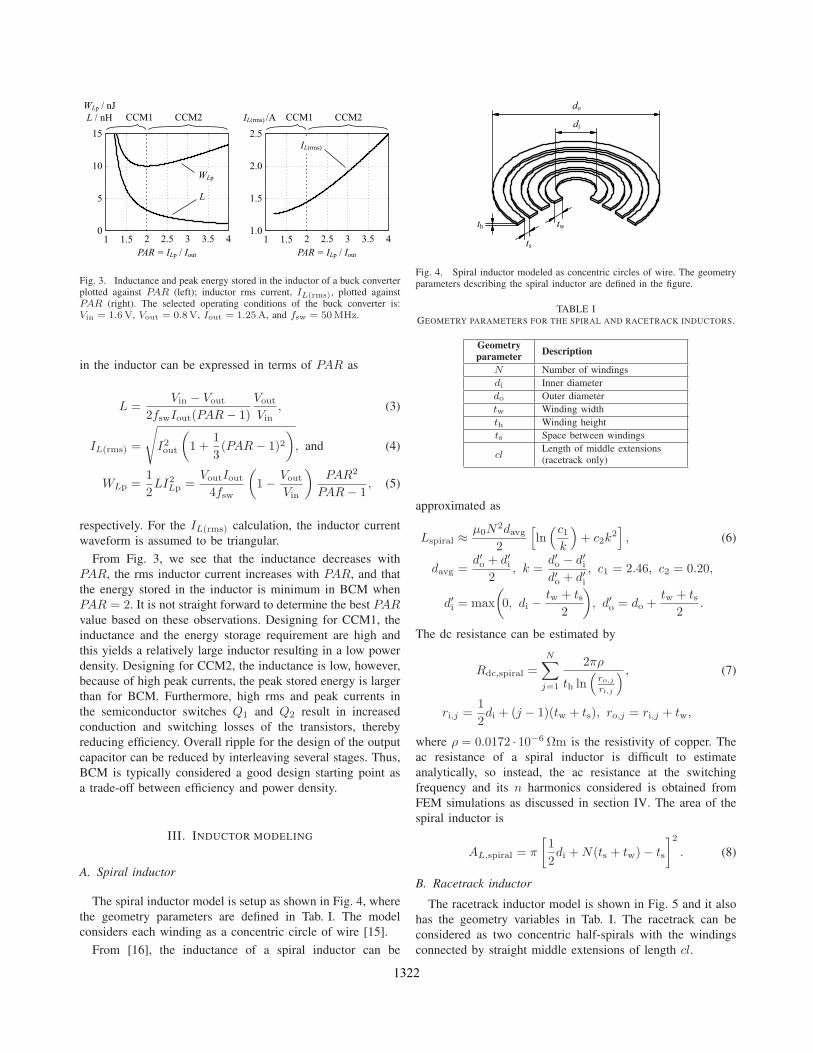
A. Spiral inductor
The spiral inductor model is setup as shown in Fig. 4, where
the geometry parameters are defined in Tab. I. The model
considers each winding as a concentric circle of wire [15].
From [16], the inductance of a spiral inductor can be
do
di
th
ts
tw
Fig. 4. Spiral inductor modeled as concentric circles of wire. The geometryparameters describing the spiral inductor are defined in the figure.
TABLE IGEOMETRY PARAMETERS FOR THE SPIRAL AND RACETRACK INDUCTORS.
Geometryparameter
Description
N Number of windings
di Inner diameter
do Outer diameter
tw Winding width
th Winding height
ts Space between windings
clLength of middle extensions(racetrack only)
approximated as
Lspiral ≈µ0N
2davg2
[
ln(c1k
)
+ c2k2]
, (6)
davg =d′o + d′i
2, k =
d′o − d′id′o + d′i
, c1 = 2.46, c2 = 0.20,
d′i = max
(
0, di −tw + ts
2
)
, d′o = do +tw + ts
2.
The dc resistance can be estimated by
Rdc,spiral =
N∑
j=1
2πρ
th ln(
ro,jri,j
) , (7)
ri,j =1
2di + (j − 1)(tw + ts), ro,j = ri,j + tw,
where ρ = 0.0172 · 10−6 Ωm is the resistivity of copper. The
ac resistance of a spiral inductor is difficult to estimate
analytically, so instead, the ac resistance at the switching
frequency and its n harmonics considered is obtained from
FEM simulations as discussed in section IV. The area of the
spiral inductor is
AL,spiral = π
[
1
2di +N(ts + tw)− ts
]2
. (8)
B. Racetrack inductor
The racetrack inductor model is shown in Fig. 5 and it also
has the geometry variables in Tab. I. The racetrack can be
considered as two concentric half-spirals with the windings
connected by straight middle extensions of length cl.
1322

th
ts
tw
cl
di / 2do
Fig. 5. Racetrack inductor model, which has the same geometry parametersas the spiral with the addition of cl to describe the length of the middleextensions.
The dc resistance of the racetrack inductor can be estimated
from the dc resistance of the spiral inductor in (7) with an
additional term that takes the middle extensions into account
Rdc,racetrack = Rdc,spiral +2 ρ cl
th
N∑
j=1
1
ro,j − ri,j. (9)
There is no analytical expression for the inductance nor for
the ac resistance of racetrack inductors available, so both are
estimated by the FEM simulations. The area of the racetrack
inductor is
AL,racetrack = AL,spiral + cl[
di + 2N(ts + tw)− ts]
. (10)
IV. INDUCTOR OPTIMIZATION PROCEDURE
The inductor optimization procedure presented in this paper
is illustrated by the flowchart shown in Fig. 6. The procedure
input is the converter operating conditions: input voltage Vin,
output voltage Vout, output current Iout, and inductor current
peak to average ratio PAR. Next, the inductor type is chosen
and the design space of inductors to be simulated is defined by
the minimum and maximum value of each geometry parameter
from Tab. I. Additionally, an incremental step size can be set
for each geometry parameter.
The first set, i = 1, of geometry parameters is loaded into
a generic inductor model in a FEM simulator and a dc
simulation is run to extract the dc inductance Ldc,i and the
dc resistance Rdc,i. The surface area AL,i is also determined
using (8) or (10), depending on which inductor type is being
simulated. The switching frequency fsw,i is calculated based
on Ldc,i and the converter operating conditions. A FEM
simulation is run at the switching frequency and each of the
n harmonics considered, and an ac resistance Rac,ij for each
harmonic, j = 1 . . . n, is extracted. From the initial operating
conditions, the inductor current waveform, which is assumed
to be triangular, can be determined. The rms value of the
inductor current at each harmonic IL(rms),ij is found from
the Fourier series expansion of the a priori known current
waveform. The total power loss Pl,i in the inductor can then
be estimated by
Pl,i = I2outRdc,i + I2L(rms),i1Rac,i1 + . . .
+ I2L(rms),inRac,in. (11)
Define i=1,2,...k geometry parameter sets.
Parameters: Ni, di,i, tw,i, th,i, ts,i, cli.
Set operating conditions of the buck converter.
Parameters: Vin, Vout, Iout, PAR.
Load the i’th geometry parameter set
to the generic FEM simulator inductor model.
DC simulation.
Output parameters: Rdc,i, Ldc,i, AL,i.
NiNN , di,dd i, tw,tt i, t
geome
M simu
geometry pa
N d t t
s: VinVV , VoutVV , I
NiN di,dd i t i t
M simulator
simulation.simulation.
rameters: R
M simulator
Determine fsw,i from Ldc,i and operating conditions.
rameters: Rdc,i, rameters: Rdc,i
Ldc,i and ope
AC simulations at fsw,i, 2fsw,i, ... nfsw,i.
Output parameters: Rac,i1, Rac,i2, ... Rac,in.
ns at ns at ns at fffsw,ff i, 222fff222 sw,ff
eters: R R
Determine αi and ηi.
ns.
noi = i + 1Is i = k ?
eters: Rac,i1, Reters: R i1 R
ermine αi and
Generate α - η Pareto front.η reto f
h,i, s,i,
paramete
or inductor
i,i, w,i,
ometry pa
imulator imulator
i = 1
erate αα - η Paret
yes
Fig. 6. Flowchart of optimization procedure.
Finally, the efficiency ηi and area-related power density αi for
the i’th geometry parameter set are calculated as
ηi =Po,i
Po,i + Pl,iand (12)
αi =Po,i
AL,i
, (13)
respectively.
After having determined ηi and αi of the first geometry
set, the next set, i = i+ 1, is loaded into the model and
the procedure is repeated. The entire inductor optimization
procedure is completed when all predefined sets of geometry
variables have been processed. Thereafter, the highest effi-
ciency inductor given an area-related power density is found
by searching the simulated data, and the α− η Pareto front is
generated. The geometry parameters for the inductors forming
the Pareto front can then be extracted for practical realizations.
The optimization procedure is repeated for each investigated
inductor type, which requires its own generic FEM simulator
model.
V. EVALUATION AND VERIFICATION OF THE INDUCTOR
OPTIMIZATION PROCEDURE
The inductor optimization procedure described in the pre-
vious section is performed with the following example buck
converter operating conditions:
1323
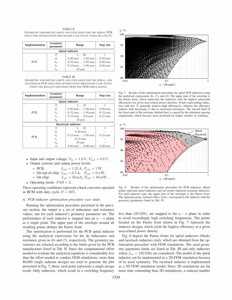
TABLE IIGEOMETRY PARAMETER LIMITS AND STEP SIZES FOR THE SPIRAL PCBINDUCTOR OPTIMIZATION PROCEDURE CASE STUDY USING (6) AND (7).
ImplementationGeometryparameter
Range Step size
Spiral inductor
PCB
N 1 . . . 20 1
di 0.30mm . . . 1.80mm 0.25mm
tw 0.15mm . . . 1.95mm 0.05mm
ts 0.15mm . . . 1.95mm 0.05mm
th 35µm −
TABLE IIIGEOMETRY PARAMETER LIMITS AND STEP SIZES FOR THE SPIRAL AND
RACETRACK PCB INDUCTOR OPTIMIZATION PROCEDURE CASE STUDY
USING THE RESULTS OBTAINED FROM THE FEM SIMULATIONS.
ImplementationGeometryparameter
Range Step size
Spiral inductor
PCB
N 1 . . . 10 1
di 0.30mm . . . 1.80mm 0.50mm
tw 0.15mm . . . 1.95mm 0.15mm
ts 0.15mm . . . 0.9mm 0.15mm
th 35µm −
Racetrack inductor
PCB
N 1 . . . 10 1
di 0.30mm −
tw 0.15mm . . . 1.95mm 0.15mm
ts 0.15mm −
th 35µm −
cl 0.20mm . . . 2.00mm 0.20mm
• Input and output voltage: Vin = 1.6V, Vout = 0.8V.
• Output currents and output power levels:
– PCB: Iout = 1.25A, Pout = 1W.
– On-top-of-chip: Iout = 0.5A, Pout = 0.4W.
– On-chip: Iout = 50mA, Pout = 40mW.
• Operating mode: PAR = 2.
These operating conditions represent a buck converter operated
in BCM with duty cycle D = 50%.
A. PCB inductor optimization procedure case study
Running the optimization procedure presented in the previ-
ous section, the output is a set of inductance and resistance
values; one for each inductor’s geometry parameter set. The
performance of each inductor is mapped into an η − α plane
as a single point. The upper part of the envelope around all
resulting points defines the Pareto front.
The optimization is performed for the PCB spiral inductor
using the analytical expressions for the dc inductance and
resistance given in (6) and (7), respectively. The geometry pa-
rameters are selected according to the limits given by the PCB
manufacturer listed in Tab. II. Since the computational effort
needed to evaluate the analytical equations is considerably less
than the effort needed to conduct FEM simulations, more than
80,000 single inductor designs are used to generate the plot
presented in Fig. 7; there, each point represents a single design
result. Only inductors, which result in a switching frequency
80
85
90
95
100
η / %
α / (W/mm2)
0.01 0.1 1
Fig. 7. Results of the optimization procedure for spiral PCB inductors usingthe analytical expressions (6), (7), and (8). The upper part of the envelope isthe Pareto front, which represents the inductors with the highest achievableefficiencies for given area-related power densities. Points representing induc-tors with low N generally achieve high efficiencies, whereas the efficiencyreduces with increasing N due to increased resistances. The inward bend ofthe lower part of the envelope (dashed line) is caused by the minimum spacingrequirement, which become more profound for higher number of windings.
80
85
90
95
100
η / %
α / (W/mm2)
0.01 0.1 1
Spiral
Racetrack
Fig. 8. Results of the optimization procedure for PCB inductors. Blackpoints represent spiral inductors and red points represent racetrack inductors.For each inductor type, the upper part of the envelope is the Pareto front.The optimum point, marked with a circle, correspond to the inductor with thegeometry parameters listed in Tab. IV.
less than 100MHz, are mapped to the η − α plane in order
to avoid exceedingly high switching frequencies. The points
located on the Pareto front shown in Fig. 7 represent the
inductor designs which yield the highest efficiency at a given
area-related power density.
Fig. 8 depicts the Pareto fronts for spiral inductors (black)
and racetrack inductors (red), which are obtained from the op-
timization procedure with FEM simulations. The used geom-
etry parameter limits are listed in Tab. III and only inductors
where fsw < 100MHz are considered. The model of the spiral
inductor can be implemented in a 2D FEM simulation because
of its axial symmetry. The racetrack inductor is implemented
as a 3D FEM simulation model. Since 3D simulations are far
more time consuming than 2D simulations, a reduced number
1324

TABLE IVGEOMETRY PARAMETERS AND SIMULATION RESULTS FOR THE OPTIMUM
SPIRAL PCB INDUCTOR.
Geometryparameter
ValueOutput
parameterSimulation
value
N 2 L 2.7 nH
di 0.30mm η 95.4%
do 1.20mm α 0.88W/mm2
tw 0.15mm fsw 58MHz
th 35µm Rdc 15mΩ
ts 0.15mm Rac @ fsw 43mΩ
TABLE VGEOMETRY PARAMETER LIMITS AND STEP SIZES FOR THE
ON-TOP-OF-CHIP AND ON-CHIP SPIRAL INDUCTOR OPTIMIZATION
PROCEDURE CASE STUDY.
ImplementationGeom.par.
Range / PointsStepsize
On-top-of-chip
N 1 . . . 10 1
di 40µm, 70µm, 120µm,200µm
−
tw 10µm . . . 100µm∧tw/th ≥ 1 18µm
ts 10µm . . . 100µm ∧ ts/th ≥ 1 18µm
th 10µm . . . 100µm 18µm
On-chip
N 1 . . . 35 1
di 20µm, 40µm, 100µm,200µm, 400µm
−
tw 2µm, 4µm, 6µm, 8µm,10µm, 12µm, 15µm, 20µm,
30µm, 50µm
−
ts 1.8µm, 3µm, 5µm −
th 3µm −
of geometry parameter sets is used for the racetrack inductor
optimization. The optimization results obtained from the FEM
simulations consider ac losses, and therefore the efficiencies
shown in Fig. 8 are less than the calculated efficiencies based
on (7) and depicted in Fig. 7.
From a direct comparison between the two inductor types,
the spiral is found to outperform the racetrack with respect
to both efficiency and area-related power density. A close
inspection of the results reveals that the best performing
racetrack inductors have minimum cl; that is, they are close
to being spiral inductors. Still, the racetrack inductor remains
attractive for inductors with a magnetic core.
The selected optimized PCB inductor is marked with a circle
in Fig. 8, and data for this particular inductor is summarized in
Tab. IV. The power loss of this inductor is pl = 42mW/mm2,
and active cooling is required; however, pl is considerably less
than typical losses of advanced microprocessors, which are in
the range of 500mW/mm2.
B. On-top-of-chip and on-chip spiral inductor optimization
procedure case study
For the on-top-of-chip and on-chip implementations, only
the spiral inductor is considered since the results obtained
from the PCB inductor in section V-A showed that the coreless
racetrack inductor is inferior to the spiral inductor. The geom-
etry parameter limits, listed in Tab. V, are considered to be
TABLE VIGEOMETRY PARAMETERS AND SIMULATION RESULTS FOR THE SELECTED
INDUCTORS FOUND WITH THE INDUCTOR OPTIMIZATION PROCEDURE FOR
THE ON-TOP-OF-CHIP REALIZATION.
Geometryparameter
ValueOutput
parameterSimulation
value
On-top-of-chip realization, domain I (fsw ≤ 100MHz)
N 4 L 4.3 nH
di 70µm η 94.4%
do 714µm α 1.0W/mm2
tw 46µm fsw 91MHz
th 46µm Rdc 40mΩ
ts 46µm Rac @ fsw 124mΩ
On-top-of-chip realization, domain II (fsw ≤ 200MHz)
N 3 L 2.3 nH
di 120µm η 94.5%
do 508µm α 1.97W/mm2
tw 46µm fsw 170MHz
th 28µm Rdc 40mΩ
ts 28µm Rac @ fsw 132mΩ
On-top-of-chip realization, domain III (fsw ≤ 500MHz)
N 2 L 0.81 nH
di 120µm η 95.8%
do 324µm α 4.85W/mm2
tw 28µm fsw 480MHz
th 28µm Rdc 31mΩ
ts 46µm Rac @ fsw 109mΩ
TABLE VIIGEOMETRY PARAMETERS AND SIMULATION RESULTS FOR THE SELECTED
INDUCTORS FOUND WITH THE INDUCTOR OPTIMIZATION PROCEDURE FOR
THE ON-CHIP REALIZATION.
Geometry
parameterValue
Output
parameter
Simulation
value
On-chip realization, domain II (fsw ≤ 500MHz)
N 6 L 9.1 nH
di 100µm η 89.6%
do 478µm α 0.22W/mm2
tw 30µm fsw 410MHz
th 3µm Rdc 1.0Ω
ts 1.8µm Rac @ fsw 1.9Ω
On-chip realization, domain III (fsw ≤ 1GHz)
N 6 L 4.1 nH
di 40µm η 89.7%
do 238µm α 0.90W/mm2
tw 15µm fsw 907MHz
th 3µm Rdc 1.0Ω
ts 1.8µm Rac @ fsw 1.9Ω
representative for practical realizations. For the on-top-of-chip
implementation, the wire width and spacing are restricted to be
greater than or equal to the wire thickness for practical reasons.
The resulting Pareto fronts are shown in Fig. 9, where the
dark gray, medium gray, and light gray domains, I, II, and III,
represent various maximum converter switching frequencies.
The increase in allowable switching frequency, compared to
100MHz for the PCB implementation, shows the inductor’s
performance gain in power density. The on-top-of-chip Pareto
front in Fig. 9(a) has higher area-related power density com-
pared to the PCB implementation in Fig. 8. Since the converter
1325

0.5 1 10 5080
85
90
95
100
η / %
α / (W/mm2)
fsw = 500 MHz
fsw = 200 MHz
fsw = 100 MHz
I II III
(a)
0.05 0.1 1 580
85
90
95
100
η / %
α / (W/mm2)
fsw = 1 GHz
fsw = 500 MHz
fsw = 200 MHz
II
I
III
(b)
Fig. 9. Spiral inductor Pareto fronts for (a) on-top-of-chip implementationand (b) on-chip implementation. The shadings correspond to a specifiedmaximum switching frequency of the buck converter.
operating conditions are fixed, then the inductance required
decreases with frequency from (3). Because of the less coarse
geometry parameter limits of the on-top-of-chip inductor com-
pared to the PCB inductor, the required inductance can be
implemented using less area, thereby increasing the power
density. According to the Pareto front, the reduced area has
only a slight impact on efficiency compared to the Pareto
front of the PCB inductor. However, transistor switching losses
increase with switching frequency, and therefore surface and
loss models of the complete buck converter are needed to
determine the optimal switching frequency with respect to
maximum efficiency and / or power density.
The on-top-of-chip implementation in Fig. 9(a) is seen to
perform better than the on-chip implementation in Fig. 9(b).
This is mainly due to the thin metal layers available in
advanced submicron semiconductor processes being a very
limiting geometry parameter. Only for very high switching
frequencies does the on-chip implementation perform well,
but such frequencies are typically not feasible due to increased
switching losses of the transistors.
As an example, the optimized inductors are selected based
No. 1 No. 2 No. 3
without ground plane with ground plane
Fig. 10. Printed Circuit Board (PCB) spiral inductors produced to verify theinductor optimization procedure. The surface of each inductor is 1.5mm2.
TABLE VIIICOMPARISON OF CALCULATED, SIMULATED, AND MEASURED
INDUCTANCES OF THE OPTIMUM SPIRAL PCB INDUCTOR FROM TABLE IV.
CalculatedValue
SimulatedValue
No. 1Measured
No. 2Measured
No. 3Measured
2.4 nH 2.7 nH 3.1 nH 2.8 nH 3.1 nH
on a predefined efficiency, which is chosen to be η = 95%for the on-top-of-chip implementation and η = 90% for the
on-chip implementation. The best fitting inductors are marked
with circles in Fig. 9(a) and 9(b); the data of these inductors
are summarized in Tab. VI and Tab. VII, respectively. The
most favorable inductor is the on-top-of-chip implementation
that achieves an efficiency of 94.5% and an area-related power
density of 1.97W/mm2 at a switching frequency of 170MHz.This selection is based on the assumption that a maximum
switching frequency of 200MHz represents a reasonable value
for an on-top-of-chip realization.
C. Experimental verification of spiral PCB inductors
The optimum inductor with geometry parameters from
Tab. IV are produced on the PCB shown in Fig. 10 to verify
the presented inductor optimization procedure. The inductor
labeled No. 1 is the practical realization of the optimum induc-
tor. No. 2 inductor realization is the same inductor but with a
via included in the center point, and No. 3 inductor realization
is equivalent to No. 1, but with a ground plane underneath to
investigate whether this influences the impedance within the
considered frequency range.
The inductor measurements are performed with an Agilent
4395A impedance analyzer using a model 40A, 1mm pitch
Picoprobe from GGB Industries, Inc. The calculated, simu-
lated, and measured inductances are compared in Tab. VIII.
Moreover, the resistances over frequency have been measured;
however, these measurement results are not considered to be
meaningful due to a distinctive scattering caused from the
contact resistance of the probe, which changes depending on
contact pressure, and due to the inductors’ impedance angles,
ϕ = arg(R+ jωL), being close to 90.
The calculated inductance is obtained with the parameters of
the optimum inductor given in Tab. IV being inserted into (6).
The error between the calculated and simulated inductance
is due to the FEM simulation model, which considers the
spiral inductor as concentric circles; this simplification yields
reduced accuracy if a low number of turns is used together
with a small inner diameter.
1326

10 20 30 40 50 60 70 80 90 100
5
4
3
2
1
0
L / nH
f / MHz
Inductor No. 1
Inductor No. 2
Inductor No. 3
Fig. 11. Measured inductance over frequency of the three PCB inductors.
The measured inductance values are higher than the calcu-
lated and simulated values. However, also the surface area of
the realized inductors, which is 1.5mm2, is higher than the
calculated value of 1.1mm2. With some tuning of the PCB
layout, e.g. using N = 1.85 turns, the inductance is expected
to approach the desired value of 2.7 nH and the surface is
reduced to 1.3mm2. The remaining difference in surface area
is due to the simplification of concentric circles used.
The measured inductances over frequency are shown in
Fig. 11. It is seen that the ground plane in No. 3 has no influ-
ence within the measured frequency band compared to No. 1.
For No. 2, the center via eff shortens the wire length resulting
in a slightly lower inductance value compared to No. 1 and
No. 3. All inductances decrease by approximately 5% within
the measured frequency range due high frequency effects.
VI. CONCLUSIONS
This paper presents an inductor optimization procedure for
Power Supply in Package (PSiP) and Power Supply on Chip
(PwrSoC) applications. Inductor implementations considered
are Printed Circuit Board (PCB) inductors, on-top-of-chip
inductors, and on-chip inductors. Inductor types investigated
are the coreless spiral and coreless racetrack inductors. The
optimization procedure uses a Finite Element Method (FEM)
simulator environment to compute efficiency and area-related
power density of an inductor given a set of geometry param-
eters. Based on the simulations, the most efficient inductor
design for a given area-related power density is determined.
The inductor optimization procedure is performed on two
case studies: spiral and racetrack PCB inductors, and spiral
on-top-of-chip and on-chip inductors. For PCB inductors, the
spiral inductor is found to outperform the racetrack inductor
in both efficiency and area-related power density for PSiP
applications. For on-top-of-chip and on-chip inductors, the on-
top-of-chip solution is found to be better suited for PwrSoC
applications since the metal layers used for on-chip inductors
are too thin, and thereby too resistive, to give sufficiently high
efficiency at feasible operating frequencies.
The most promising spiral PCB inductor was fabricated and
measured to verify the proposed inductor optimization proce-
dure.
ACKNOWLEDGMENT
The authors would like to thank Dr. T. Morf and Dr. H.
Rothuizen from IBM Research Lab., Rueschlikon, Zurich,
Switzerland, for allowing access to their measurement equip-
ment and for guidance with the measurement setup.
REFERENCES
[1] “International technology roadmap for semiconductors,” 2009. [Online].Available: www.itrs.net
[2] L. Chang, R. K. Montoye, B. L. Ji, A. J. Weger, K. G. Stawiasz,and R. H. Dennard, “A fully-integrated switched-capacitor 2:1 voltageconverter with regulation capability and 90% efficiency at 2.3 A/mm2,”in IEEE Symposium on VLSI Circuits (VLSIC 2010), Honolulu, Hawaii,16–18 June 2010, pp. 55–56.
[3] R. Foley, F. Waldron, J. Slowey, A. Alderman, B. Narveson, and S. C.O’Mathuna, “Technology roadmapping for power supply in package(psip) and power supply on chip (pwrsoc),” in Proc. of the 25th IEEE
Annual Applied Power Electronics Conference and Exposition (APEC
2010), Palm Springs, CA, 21–25 Feb. 2010, pp. 525–532.[4] V. W. Ng, M. D. Seeman, and S. R. Sanders, “High-efficiency,
12V-to-1.5V dc-dc converter realized with switched-capacitor architec-ture,” in Symposium on VLSI Circuits, Kyoto, Japan, 16–18 June 2009,pp. 168–169.
[5] S. Mathúna, T. O’Donnell, N. Wang, and K. Rinne, “Magnetics onsilicon: an enabling technology for power supply on chip,” IEEE Trans.
on Power Electron., vol. 20, no. 3, pp. 585–592, May 2005.[6] P. Hazucha, G. Schrom, J. Hahn, B. A. Bloechel, P. Hack, G. E. Dermer,
S. Narendra, D. Gardner, T. Karnik, V. De, and S. Borkar, “A 233 MHz80%-87% efficient four-phase dc-dc converter utilizing air-core inductorson package,” IEEE Trans. on Solid-State Circuits, vol. 40, no. 4, pp.838–845, April 2005.
[7] G. Schrom, P. Hazucha, F. Paillet, D. J. Rennie, S. T. Moon, D. S.Gardner, T. Kamik, P. Sun, T. T. Nguyen, M. J. Hill, K. Radhakrishnan,and T. Memioglu, “A 100MHz eight-phase buck converter delivering12A in 25mm2 using air-core inductors,” in Proc. of the 22nd IEEE
Annual Applied Power Electronics Conference (APEC 2007), Anaheim,CA, 25 Feb.–1 March 2007, pp. 727–730.
[8] J. Wibben and R. Harjani, “A high-efficiency dc–dc converter using 2 nHintegrated inductors,” IEEE Trans. on Solid-State Circuits, vol. 43, no. 4,pp. 844–854, April 2008.
[9] R. Meere, T. O’Donnell, H. Bergveld, N. Wang, and S. O’Mathuna,“Analysis of microinductor performance in a 20-100 MHz dc/dc con-verter,” IEEE Trans. on Power Electron., vol. 24, no. 9, pp. 2212–2218,Sept. 2009.
[10] C. R. Sullivan, “Integrating magnetics for on-chip power: Challengesand opportunities,” in Proc. of the IEEE Custom Integrated Circuits
Conference (CICC 2009), San Jose, CA, 13–16 Sept. 2009, pp. 291–298.
[11] Texas Instruments, “TPS3002 datasheet,” 2008. [Online]. Available:http://focus.ti.com/docs/prod/folders/print/tps63002.html
[12] T. H. Lee, The design of CMOS radio-frequency integrated circuits.Cambridge University Press, 2004.
[13] J. Qiu and C. R. Sullivan, “Inductor design for VHF tapped-inductor dc-dc power converters,” in Proc. of the 26th IEEE Annual Applied Power
Electronics Conference and Exposition (APEC 2011), Fort Worth, TX,6–11 March 2011, pp. 142–149.
[14] J. W. Kolar, J. Biela, and J. Miniböck, “Exploring the Pareto frontof multi-objective single-phase PFC rectifier design optimization-99.2%efficiency vs. 7kW/dm3 power density,” in Proc. of the 6th International
Power Electronics and Motion Control Conference (IPEMC 2009),Wuhan, China, 17–20 May 2009.
[15] R. Rodriguez, J. Dishman, F. Dickens, and E. Whelan, “Modelingof two-dimensional spiral inductors,” IEEE Trans. on Components,
Hybrids, and Manufacturing Technology, vol. 3, no. 4, pp. 535–541,Dec 1980.
[16] S. S. Mohan, M. del Mar Hershenson, S. Boyd, and T. Lee, “Simpleaccurate expressions for planar spiral inductances,” IEEE Trans. on
Solid-State Circuits, vol. 34, no. 10, pp. 1419–1424, Oct. 1999.
1327