in the mosfet gm/id characteristic - scielo colombia son necesarios procedimientos precisos de...
TRANSCRIPT

Tecnura • p-ISSN: 0123-921X • e-ISSN: 2248-7638 • Vol. 21 Número 52 • Abril - Junio de 2017 • pp. 32-44[ 32 ]
Tecnurahttp://revistas.udistrital.edu.co/ojs/index.php/Tecnura/issue/view/819
DOI: http://dx.doi.org/10.14483/udistrital.jour.tecnura.2017.2.a02
InvestIgacIón
AbstractContext: In advanced ultralow-power devices, it is necessary to use the accuracy extraction procedures of the MOSFET threshold voltage to fully characte-rize the devices. These procedures are based in the measurement of the Tran-conductance efficiency (gm/ID) and its first derivative in function of the vol-tage gate source (d(gm/ID)/dVGS). In order to increa-se their independency respect to the non-zero drain source voltage (VDS ≠0) it is used a process to correct the error. Theoretically, VDS should be 0 V; however, the VDS is grater than 10 mV in the experimental se-tup in order to avoid electrical noise, but less than a certain maximum value for allowing the MOSFET operation in the linear region of the weak inversion.Objective: To compare the extraction procedure proposed by (MC Schneider et al., 2006) and the method proposed by (Rudenko et al., 2011) with a generic, controlled and coherent test scenario.Method: This paper proposes a test scenario based on the Advanced Compact MOSFET model (ACM) of a long channel MOSFET made in a standard 0.35 mm CMOS process, implemented numerically in MAT-LABâ. The concept of Power Error Correction (PEC) was used to compare the two processes numerically;
it quantifies the sensitivity of the extraction process to the effect by the non-zero voltage value of the VDS in the experimental setup (i.e., NZ-DS effect).Results: The error correction procedure proposed by (Siebel et al., 2012, Schneider et al., 2006) estimates the NZ-DS effect better than the procedure proposed by (Rudenko et al., 2011), considering the average, maximum and minimum PEC obtained for both ex-traction methodologies for a long channel MOSFET fabricated in a standard CMOS process of 0.35 μm, when the VDS is less than 50 mV.Conclusions: The Vth extraction procedure proposed by (MC Schneider et al., 2006) is more robust than the method proposed by (Rudenko et al., 2011) re-garding the NZ-DS effect.Keywords: Threshold Voltage Extraction, MOSFET Modeling, Gm/ID transconductance efficiency.
ResumenContexto: En los dispositivos de ultrabaja poten-cia son necesarios procedimientos precisos de ex-tracción de voltaje de umbral del MOSFET. Estos se basan en la medición de la eficiencia de la trans-conductancia (gm/ID) y su primera derivada respec-to al voltaje puerta-fuente (d(gm/ID)/ dVGS). Para
Comparative analysis of threshold voltage extraction techniques based in the MOSFET gm/ID characteristic
Comparación de las técnicas de extracción del voltaje de umbral basadas en la característica gm/ID del MOSFET
Arturo Fajardo Jaimes1
Fecha de recepción: 4 de febrero de 2016 Fecha de aceptación: 15 de febrero de 2017
Cómo citar: Fajardo J., A. (2017). Comparación de las técnicas de extracción del voltaje de umbral basadas en la característica gm/ID del MOSFET. Revista Tecnura, 21(52), 32-44. doi: 10.14483/udistrital.jour.tecnura.2017.2.a02
1 Ingeniero electrónico, magíster en Electrónica. Profesor Asistente Pontificia Universidad Javeriana. Bogota, Colombia. Contacto: [email protected]

Comparación de las técnicas de extracción del voltaje de umbral basadas en la característica gm/ID del MOSFET
Fajardo j., a.
Tecnura • p-ISSN: 0123-921X • e-ISSN: 2248-7638 • Vol. 21 Número 52 • Abril - Junio de 2017 • pp. 32-44[ 33 ]
INTRODUCTION
Power consumption awareness began in the nine-ties. Nowadays, every circuit has to face the power consumption issue in both portable devices (e.g., for increasing the battery life) and high-end circuits (e.g., for avoiding packages and reliability issues). The advances in the solid-state devices had a di-rect impact in the efficiency and the cost of the electronic equipment (Sarmiento 2004); in particu-lar, high-efficient systems such as inverters (Fajar-do et al. 2014) and power supplies (Hernández et al. 2012) have been explored using high-frequency power MOSFET (i.e., Metal-Oxide-Semiconductor Field-Effect Transistor). Considering the micro-sca-le electronic systems, the power consumption has had a big reduction since the first integrate circuit; furthermore, the power reduction started with the invention of the complementary metal–oxide–se-miconductor (CMOS) technology that allows the reduction of the static power consumption. The
designing of integrate circuits using ultra-low power techniques, such as supply voltage reduc-tion, sub threshold operation, and Biasing MOS-FETs at very low current are not rare nowadays. Consequently, there have been dedicated propo-sed models for modeling the MOSFET in all its operation regions, including weak, moderate and strong inversion (Schneider et al. 2010).
The estimation of the MOSFET threshold vol-tage (Vth) is critical to model the complementary metal–oxide–semiconductor (CMOS) circuits, par-ticularly on the design of ultra-low-power devices (Rudenko et al. 2011), (Siebel et al. 2012). The Vth is basically the gate source voltage (VGS) level ne-cessary in the MOSFET to start working in Strong Inversion (SI). To identify a hard threshold in the drain current (ID) vs. gate source voltage (VGS) characteristic is difficult, because the continuous nature of the involved physical phenomena. The-refore, many researches have proposed Vth defini-tions and extraction procedures (Siebel et al. 2012).
aumentar en algunas decenas de mV la precisión del voltaje de umbral extraído, se recurre a un proceso de corrección de errores que disminuye la influen-cia del voltaje dreno-fuente (VDS) que teóricamente debería ser 0 V. Típicamente, en el montaje experi-mental, el VDS es mayor a 10 mV con el fin de evi-tar el ruido eléctrico, pero menor a un cierto valor máximo con el fin de permitir que el MOSFET siem-pre opere en su región lineal.Objetivo: Comparar el procedimiento de extracción propuesto por Schneider et al. (2006) y el método propuesto por Rudenko et al. (2011) con un esce-nario de prueba genérico, controlado y coherente.Método: Se implementó un escenario de prueba en el software Matlab para un MOSFET de canal largo fabricado en un proceso estándar CMOS de 0,35 mm, usando el modelo Advanced Compact MOSFET (ACM). Para comparar los dos procesos de extracción se tomó el concepto de potencia de co-rrección del error (PEC), el valor de este cuantifica la
sensibilidad del proceso de extracción con respecto al valor no 0V del VDS usado experimentalmente (i.e., efecto NZ-DS).Resultados: Considerando el promedio, el máximo y el mínimo PEC obtenido para ambas metodolo-gías de extracción, el procedimiento de corrección de errores propuesto en Siebel, Schneider y Galup (2012) y Schneider et al. (2006) estima el efecto NZ-DS mejor que el procedimiento propuesto en Ru-denko et al. (2011) para un MOSFET de canal largo fabricado en un proceso estándar CMOS de 0,35 μm, cuando el VDS es inferior a 50 mV.Conclusiones: El procedimiento de extracción de Vth propuesto por Schneider et al. (2006) es más ro-busto que el sugerido en Rudenko et al. (2011) con respecto al efecto NZ-DS.Palabras clave: extracción del voltaje de umbral, modelamiento de MOSFET, eficiencia transconduc-tancia Gm/ID.

Comparación de las técnicas de extracción del voltaje de umbral basadas en la característica gm/ID del MOSFET
Fajardo j., a.
Tecnura • p-ISSN: 0123-921X • e-ISSN: 2248-7638 • Vol. 21 Número 52 • Abril - Junio de 2017 • pp. 32-44[ 34 ]
The extraction procedures generally use the ID vs. VGS characteristic of the MOSFET (Ortiz-Conde et al. 2002). Furthermore, most of them use only one regime of operation (i.e., ID–VG methods), the SI region or the Weak Inversion (WI) region in both its linear and saturation operation. However, the Vth extracted data using these approaches is inaccura-te because the Vth occurs in the transition region between WI and SI (Schneider et al. 2010).
Recently, new physic-based Vth definitions have been proposed because of the introduction of char-ge-based models (Schneider et al. 2010). In ad-dition, accurate extraction methods based in the measurement of the transconductance efficiency (gm/ID) and the transconductance efficiency chan-ge (d(gm/ID)/dVG) have been proposed by (Siebel et al. 2012, Schneider et al. 2006). Parasitic effects (such as drain or source series resistances and chan-nel mobility degradation) tend to have less influen-ce in these extraction techniques. Furthermore, they are less sensitive to short channel effects such as velocity saturation. However, these charge-based definition and extraction methods can be used for finding the conventional Vth value used in the po-tential-based models. The charge-based definition of the Vth involves a physically impossible extrac-tion setup because both the gm/ID and the d(gm/ID)/dVG characteristics must be measured with the MOSFET operating at zero drain source voltage (VDS=0). However, the MOSFET in the real setup operates in its linear region with a very low volta-ge for decreasing the parasitic effects, but it is high enough to sense the ID (Schneider et al. 2010). All of these techniques propose a correction methodo-logy in order to reduce the non-zero drain-to-source (NZ-DS) effect present on the Vth extraction me-thods, but a direct comparison of these methodo-logies based in the reported results is too difficult
or even impossible to do. Recently, (Fajardo et al. 2013) proposed the power error correction (PEC) of NZ-DS effect concept to analyze the error correc-tion in these methodologies of Vth extraction.
The fundamental purpose of this paper is to compare the accuracy of the gm/ID method pro-posed by (Schneider et al. 2006) and the d(gm/ID)/dVG method proposed by (Rudenko et al. 2011), using the power error correction (PEC) concept proposed by (Fajardo et al. 2013). Additionally, this paper develops a comprehensible presentation of the NZ-DS effect using analytical models, and im-plements a generic, controlled and consistent test scenario in MATLAB for a long channel MOSFET made in a 0.35 mm CMOS standard process using the Advanced Compact MOSFET (ACM) model.
METHODOLOGY
Advanced Compact MOSFET (ACM) Model.
The ACM model represents the device behavior in all regimes of operation using an analytical equa-tion set (Schneider et al. 2006). The following are the ACM equations explored in this paper (Equa-tions (1) to (5)).
2 2
2IS ID
T IS IDox
Q QWID Q QL C n
(1)
( ) ( )(D) lnIP IS D IS DP t
ox t IP
Q Q QV VS
nC Q
(2)
2 1 ln1
thP sa F t
VG VnVn n
(3)
1
2IS ID
Tox
gmQ QID n
C
(4)
21
2 2IS ID IS ID
tIS IDox ox
t tox ox
d gm Q Q Q Qn Q QdVG ID C C n nC C
(5)

Comparación de las técnicas de extracción del voltaje de umbral basadas en la característica gm/ID del MOSFET
Fajardo j., a.
Tecnura • p-ISSN: 0123-921X • e-ISSN: 2248-7638 • Vol. 21 Número 52 • Abril - Junio de 2017 • pp. 32-44[ 35 ]
Where, µ is the mobility of the carriers in the se-miconductor substrate, C’ox is the oxide capacitance per unit area, L and W are the channel length and the channel width of the MOSFET respectively, Q’ID is the drain inversion charge density, Q’IS is the source inversion charge density, Q’IP is the pinch-off charge density, VP is the channel pinch-off voltage, φF is the Fermi potential, φsa is the surface potential, VS is the source bulk voltage, VD is the drain bulk voltage, VG is the gate bulk voltage, n is the slope factor, and φt is the thermal voltage given equation (6) as follows.
t
kTq
(6)
Where q is the elemental electron charge, k is the Boltzmann constant, and T the absolute tem-perature. A script was implemented for solving the equations (1) to (5), assuming that the MOSFET was in non-saturated operation in the WI region. Furthermore, the test scenario considered a long channel NMOS transistor (W/L=32mm/3.2mm) at a temperature of 27°C, and the technological pa-rameters of the standard 0.35 mm CMOS process (i.e., acceptor doping concentration NA= 6x1016 cm-3, oxide thickness tox=7.8 nm, low field mo-bility m0 = 0.36238 m2/V.s, and flat band voltage VFB=0.8 V). (Schneider et al. 2010) presents an analytic expression for the equilibrium threshold voltage (Vth); this expression allows the Vth calcu-lus from technological parameters, as shown in (7).
V =V +2 + 2th FB f f (7)
Where, γ is the so-called body-effect factor.
Threshold voltage (Vth) definitions
The Vth concept is directly related to the physical phenomenon that prevails in the current flow when the MOSFET goes from WI to SI. The Vth in the sur-face potential based models (Tsividis et al. 1999) is the VGS that produces a surface potential equal to twice the Fermi potential ( 2s F ). On the other hand, in the charge-based models (i.e., EKV, ACM), the Vth is the VG value associated to the threshold inversion charge density (Q’th). Addicionally, both Vth values are related by the analytic expressions (Siebel et al. 2012) summarized in table 1.
The Vth extraction is generally based in the gm/ID extraction (Siebel et al. 2012, Schneider et al. 2006) in advanced ultra-low power applications. In order to understand this methodology we must dis-cuss the gm/ID and the (d(gm/ID)/dVG) concepts using the charge-based model framework. The gm/ID is a quality factor of how much transconductan-ce (gm) is produced for a given unit of bias current (Binkley 2007). The gm/ID in the bipolar transistor device is maintained at a constant high value over multiple tens of collector current. Unfortunately, the MOSFET device gm/ID is maximum in the WI region (always less than the gm/ID of the bipolar transistor), and drops significantly when operating in the SI region (Schneider et al. 2010). The gm/ID behavior (i.e., high for MI and low for SI and soft in the transition) allows defining directly the Vth from a specific inversion charge using the ACM model.
Table 1. Charge based definition of threshold voltage summary.
Notation Vth Definition Gm/ID RPD VDS=0
Value of qI VGS=Vth
Relative difference to classical definition 2s Fφ φ=
Vthq1 I ox tQ nC φ′ ′= − 50 % 1
1 ln1tnnn
φ ⎛ ⎞⎛ ⎞+⎜ ⎟⎜ ⎟−⎝ ⎠⎝ ⎠
Vthq0.5
max m
g D
gv I
⎛ ⎞⎛ ⎞∂−⎜ ⎟⎜ ⎟⎜ ⎟∂ ⎝ ⎠⎝ ⎠ 100/3 % 0.5
( )
1 ln 0.52 1tnnn
φ⎛ ⎞⎡ ⎤⎛ ⎞⎜ ⎟+ −⎢ ⎥⎜ ⎟⎜ ⎟⎜ ⎟−⎢ ⎥⎝ ⎠⎣ ⎦⎝ ⎠
Source: own work, based on (Schneider et al. 2006).

Comparación de las técnicas de extracción del voltaje de umbral basadas en la característica gm/ID del MOSFET
Fajardo j., a.
Tecnura • p-ISSN: 0123-921X • e-ISSN: 2248-7638 • Vol. 21 Número 52 • Abril - Junio de 2017 • pp. 32-44[ 36 ]
Defining the normalized inversion charge (qI) by equations (8) and (4), we expressed the gm/ID as a function of the normalized charges in the MOS channel in equation (9). Also, using equations (8) and (2) we found the VDS as a function of the chan-nel charges in equation (10). The normalized gm/ID (gm/IDn) can be calculated using equation (11), this expression was found using equations (10) and (9), and assuming VDS=0 (i.e., MOS capacitor analysis qI= qID =qIS). As shown in figure 1(a), the gm/IDn characteristic is monolithical and without discontinuities. Therefore, the relative to the peak drop (RPD) can be used as a metric if we choose a RPD of 50% as the transition point between WI and SI, the related inversion charge would be qI=1.
; I
I IP ox tIP
Qq Q nCQ
(8)
1
1T IS ID
gmID n q q
(9)
ln ISt IS ID
ID
qVDS q qq
(10)
Where qIS is the normalized source inversion charge, and qID is the normalized drain inversion charge. Another possible approach is to analyze the d(gm/ID)/dVG MOSFET characteristic: this characteristic may be interpreted like the d(gm/ID)/dVG for a given gate voltage change. The d(gm/ID)/dVG and its normalized value (d(gm/ID)/dVG) were found as a function of the normalized chan-nel charges, following a similar procedure to the gm/ID characteristic. These are given by equations (12) and (13).
a) gm/IDn vs qI. b) d(gm/ID)/dVGn vs. qI
Figure 1. Transconductance MOSFET Characteristics.
Source: own work.
1
max
2 22 2 2nor ID IS I
gm gm gmID ID ID q q q
(11)
2 2 2 2
1 1 11 22 2 2
IS ID I
IS ID I
t IS ID t I
q q qq q qd gm
dVG ID n q q n q
(12)
1
3max
274 1
I
nor I
qd gm d gm d gmdVG ID dVG ID dVG ID q
(13)

Comparación de las técnicas de extracción del voltaje de umbral basadas en la característica gm/ID del MOSFET
Fajardo j., a.
Tecnura • p-ISSN: 0123-921X • e-ISSN: 2248-7638 • Vol. 21 Número 52 • Abril - Junio de 2017 • pp. 32-44[ 37 ]
The gm/IDn and the d(gm/ID)/dVG are plotted in figure 1. As shown in figure 1(b), d(gm/ID)/dVGn has a maximum value between WI and SI (i.e., high and low values of qI); therefore, this maxi-mum is chosen as a threshold between WI and SI operation. On the other hand, gm/IDn (figure 1(a)) does not have any particular characteristic in the transition.
The common charge-based definition of Vth is qIth=qIth0.5=0.5 or qIth=qIth1=1. If we use the qIth1 de-finition, the Vth is the voltage that produces the same drift and diffusion components of the drain current. On the contrary, if qIth0.5 is used for defi-ning the Vth, it represents the voltage that produces the maximum value of the d(gm/ID)/dVG charac-teristic. The table 1 shows the Vth definitions, the used notation, the gm/ID RPD, the value of the qI at Vth, and the voltage difference between the classi-cal and the charge Vth definitions.
Transconductance efficiency (gm/ID) methods used for Vth extraction
Some error source in gm/ID and d(gm/ID)/dVG extraction processThe test setup used for the Vth extraction pro-cess (applying the gm/ID methods) is shown in figure 2(a). The VDS was replaced from 10mV to
50mV for any VDS value the gm/ID, and the d(gm/ID)/dVG characteristics were extracted as functions of the gate voltage. Additionally to the usual error involved in any empirical measurement, the error introduced by the numerical derivatives calculus of the gm/ID, the d(gm/ID)/dVG characteristics, and the NZ-DS effect must be considered in this experimental setup. To show error influence, some normalized gm/ID curve samples (for several ID values) were calculated using the charge based ex-pressions of the ACM model (equations (1) to (5)); then these curve samples were evaluated using the numerically derivatives of the correspondent drain current samples. The resulting curves were plotted in figure 2(b) where it is possible to see the impact of the numerical error especially for low values of the gate voltage (low measured current).
This work calculates the gm/ID and d(gm/ID)/dVG characteristics using the charge-based expres-sions which are the equations (4) and (5), so the error generated by the numerical calculus of the-se characteristics is not present. Furthermore, this controlled environment permits to evaluate in an easy way the PEC for the NZ-DS effect on the ac-curacy Vth extraction for advanced ultra-low power devices proposed by (Siebel et al. 2012, Schneider et al. 2006) because it is the only error source pre-sent in the extraction methodology.
0 0.1 0.2 0.3 0.4 0.5 0.6 0.7 0.8 0.9
0
5
10
15
20
25
30
35VD =0.001
VD =0.01
VD =0.02
VD =0.03
VD =0.04
VD =0.05
VD =0.06
VD =0.07
VD =0.08
VD =0.09
VD=0.10
a) Circuit topology for measures. b) Extracted by derivative calculus.Figure 2. gm/ID characteristic.
Source: own work

Comparación de las técnicas de extracción del voltaje de umbral basadas en la característica gm/ID del MOSFET
Fajardo j., a.
Tecnura • p-ISSN: 0123-921X • e-ISSN: 2248-7638 • Vol. 21 Número 52 • Abril - Junio de 2017 • pp. 32-44[ 38 ]
In order to analyze the NZ-DS effect, figure 3 presents the gm/ID and d(gm/ID)/dVG characte-ristics calculated with the charge-based expres-sions. In figure 3(a) it is clear that the NZ-DS effect is increased by the VDS growth, therefore the Vth extracted using the operational definition (RPD of 50% or 75%) increases too. Secondly, figure 3(b) makes it clear that the NZ-DS effect is the varia-tion of the d(gm/ID)/dVG maximum point. In con-clusion, the NZ-DS effect increases the extracted Vth; this effect must be corrected in order to have better accuracy of the extraction procedures in some mV.
The Vth extraction procedures based in the gm/ID characteristic.
When the VG=Vth and VS=0 (because our cir-cuit topology qIS= qth), and using equation (8), we can rewrite equation (10) as equation (16).
ln th
th
It I ID
ID
qVD q q
q
(14)
Then, we found the gm/ID value related to the Vth charge condition as a function of the VD. Fur-thermore, we found the analytical expressions of the normalized gm/ID (i.e., gm/IDn) as a function of the VD using the common charge-based defini-tions of Vth (i.e., qIth=qIth0.5=0.5 and qIth=qIth1=1) and equations (11) and (14). These founded expressions are given by equations (15) and (16).
0 0.1 0.2 0.3 0.4 0.5 0.6 0.7 0.8 0.9 10
0.2
0.4
0.6
0.8
1
0 0.1 0.2 0.3 0.4 0.5 0.6 0.7 0.8 0.9 1
0
0.2
0.4
0.6
0.8
1
a) gm/ID vs. VG. b) d(gm/ID)/d VG vs. VG.Figure 3. Some normalized characteristic results.
Source: own work
10.5
0
2
- 22.5 0.5 exp
2nq
t
t
gmID VD
W
(15)
10 exp 1
nq
t t
gm 2ID VD VD3+exp 1- -W
(16)

Comparación de las técnicas de extracción del voltaje de umbral basadas en la característica gm/ID del MOSFET
Fajardo j., a.
Tecnura • p-ISSN: 0123-921X • e-ISSN: 2248-7638 • Vol. 21 Número 52 • Abril - Junio de 2017 • pp. 32-44[ 39 ]
Where the gm/IDnq0.5 and gm/IDnq1 are the gm/
IDn values related to the VGS (or VG) that creates a superficial inversion charge density of qIth1*Q’IP and qIth0.5*Q’IP respectively; W0 {*} is the Lambert function (Corless et al. 1996). This expression can be simpli-fied for very low values of VDS as gm/IDnq0.5 = 2/3 or gm/IDnq1=0.5. Therefore, the extraction procedures consist of determining the gate voltage (i.e., Vthq0.5 or Vthq1) at which the gm/IDn vs. VGS characteris-tic is equal to 50% or 66.66%. Then it is necessary to correct the NZ-DS effect of the extracted value. (Siebel et al. 2012, Schneider et al. 2006) reports a closed expression for calculating the incremental
error present in the gm/ID characteristic ∆(gm/ID), these errors for qIth0.5 and qIth1 are given by equations (17) and (18).
We used the incremental error in the gm/IDn and then extract the Vth (Vthq0.5 or Vthq1) by simply determining the VGS at which the gm/IDn charac-teristics are equal to the ideal condition plus the incremental error (equation (19)).
Figure 4(a) shows the ∆(gm/ID) behavior for low values of VDS, and figure 5(a) illustrates all the ex-tracting process. On the other hand, (Rudenko et al. 2011) proposes for Vthq0.5 an error correction based in the incremental error ∆Vth, given by equation (20).
0.50.5
23
m
nqnq
g gm -ID ID
(17)
10 exp 1
m
nq
t t
g 2 -0.5ID VD VD3+exp 1- -W
(18)
1(0.5) 1(0.5) 1(0.5),V 0q q DS q
m m m
n n n
g g gID ID ID
(19)
16 16ln 0.5 ln 1 1 0.25 1 32 21 exp 1 exp3 3
tD D
t t
Vth nV V
(20)
∆vg is shown in figure 4 (b). The error less Vthq0.5 is equal to the ideal condition plus the in-cremental error (equation (21)).
0.5 0.5, 0DSth th VV V Vth (21)
Where we extracted the Vthq0.5 from the gm/IDn characteristic (RPD 66.66%) or from d(gm/ID)/dVG characteristic (Vth=VGS where d(gm/ID)/dVG is maximum), then we estimate the error with equa-tion (20) and determine the Vthq0.5 using equation
(21). Figure 5(b) illustrates all the extracting proces-ses for the d(gm/ID)/dVG characteristic.
Power Error Correction in Vth extraction gm/ID Methods(Fajardo et al. 2013) defines the PEC with the fo-llowing equation (22).
0
100 1 cEPECE
(22)

Comparación de las técnicas de extracción del voltaje de umbral basadas en la característica gm/ID del MOSFET
Fajardo j., a.
Tecnura • p-ISSN: 0123-921X • e-ISSN: 2248-7638 • Vol. 21 Número 52 • Abril - Junio de 2017 • pp. 32-44[ 40 ]
Where EC is the error of the extracted Vth for a VDS sweep from 0 mV to Vmax using the correction factor of the method, and E0 is the mean of the ex-tracted Vth for the same VDS sweep without using
the correction factor. The Vmax value is a technology value for a particular analyzed device; particular-ly for the long channel NMOS transistor studied in this paper, this value was set to 50 mV.
0 20 40 60 80 1000
50
100
150
200
VDS (mV)
gm/ID
n 10
−3
qith
=0.5
qith
=1
VDS (mV)
a) ∆gm/ID b) ∆VthFigure 4. NZ-DS effect correction factor
Source: own work
a) On the gm/ID characteristic. b) On the d(gm/ID)/d characteristic.Figure 5. NZ-DS effect
Source: own work
RESULTS
Consistency Analysis of the simulation results and the extraction methods.
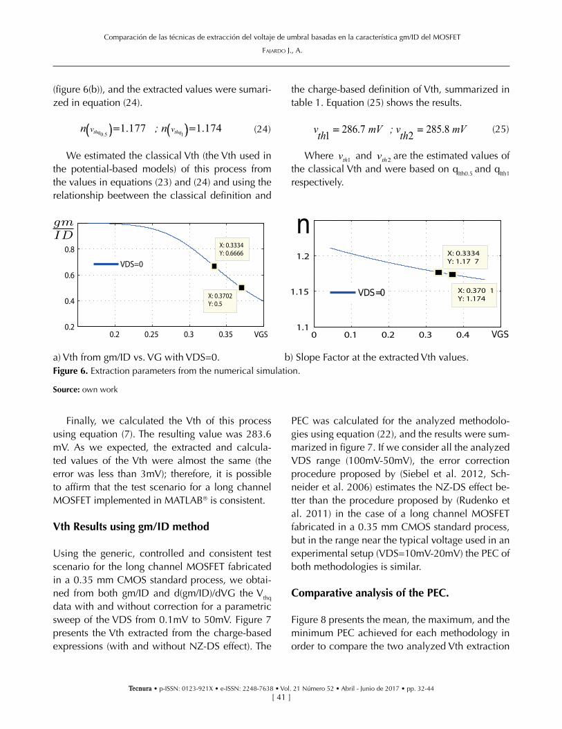
First, we extracted the Vth from the simulation data using the charge-based expressions (figure 6(a)). The extracted values were sumarized in equation (23).
0.5 1333.4 370.2thq thqv mV ; v mV (23)
Where 0.5thqv and 1thqv are the Vth extracted va-
lues using the charge-based definition qIth=qIth0.5=0.5 and qIth=qIth1=1, respectively. Second, we extrac-ted the value of the slope factor (n) for these MOS-FET operation points using the simulation data
Comparación de las técnicas de extracción del voltaje de umbral basadas en la característica gm/ID del MOSFET
Fajardo j., a.
Tecnura • p-ISSN: 0123-921X • e-ISSN: 2248-7638 • Vol. 21 Número 52 • Abril - Junio de 2017 • pp. 32-44[ 41 ]
(figure 6(b)), and the extracted values were sumari-zed in equation (24).
0.5 11.177 1.174thq thqv vn ; n
(24)
We estimated the classical Vth (the Vth used in the potential-based models) of this process from the values in equations (23) and (24) and using the relationship beetween the classical definition and
the charge-based definition of Vth, summarized in table 1. Equation (25) shows the results.
286.7 285.81 2v mV ; v mVth th (25)
Where 1thv and 2thv are the estimated values of the classical Vth and were based on qIth0.5 and qIth1 respectively.
0.2 0.25 0.3 0.35 0.40.2
0.4
0.6
0.8
1
X: 0.3702Y: 0.5
VGS
X: 0.3334Y: 0.6666
VDS=0
0 0.1 0.2 0.3 0.4 0.5
1.1
1.15
1.2
1.25
X: 0.3334Y: 1.17 7
X: 0.370 1Y: 1.174
a) Vth from gm/ID vs. VG with VDS=0. b) Slope Factor at the extracted Vth values.Figure 6. Extraction parameters from the numerical simulation.
Source: own work
Finally, we calculated the Vth of this process using equation (7). The resulting value was 283.6 mV. As we expected, the extracted and calcula-ted values of the Vth were almost the same (the error was less than 3mV); therefore, it is possible to affirm that the test scenario for a long channel MOSFET implemented in MATLAB is consistent.
Vth Results using gm/ID method
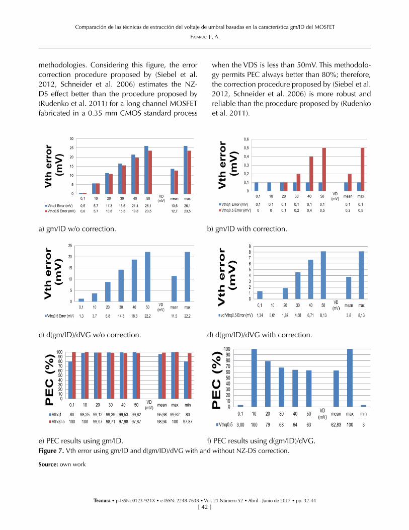
Using the generic, controlled and consistent test scenario for the long channel MOSFET fabricated in a 0.35 mm CMOS standard process, we obtai-ned from both gm/ID and d(gm/ID)/dVG the Vthq data with and without correction for a parametric sweep of the VDS from 0.1mV to 50mV. Figure 7 presents the Vth extracted from the charge-based expressions (with and without NZ-DS effect). The
PEC was calculated for the analyzed methodolo-gies using equation (22), and the results were sum-marized in figure 7. If we consider all the analyzed VDS range (100mV-50mV), the error correction procedure proposed by (Siebel et al. 2012, Sch-neider et al. 2006) estimates the NZ-DS effect be-tter than the procedure proposed by (Rudenko et al. 2011) in the case of a long channel MOSFET fabricated in a 0.35 mm CMOS standard process, but in the range near the typical voltage used in an experimental setup (VDS=10mV-20mV) the PEC of both methodologies is similar.
Comparative analysis of the PEC.
Figure 8 presents the mean, the maximum, and the minimum PEC achieved for each methodology in order to compare the two analyzed Vth extraction
Comparación de las técnicas de extracción del voltaje de umbral basadas en la característica gm/ID del MOSFET
Fajardo j., a.
Tecnura • p-ISSN: 0123-921X • e-ISSN: 2248-7638 • Vol. 21 Número 52 • Abril - Junio de 2017 • pp. 32-44[ 42 ]
methodologies. Considering this figure, the error correction procedure proposed by (Siebel et al. 2012, Schneider et al. 2006) estimates the NZ-DS effect better than the procedure proposed by (Rudenko et al. 2011) for a long channel MOSFET fabricated in a 0.35 mm CMOS standard process
when the VDS is less than 50mV. This methodolo-gy permits PEC always better than 80%; therefore, the correction procedure proposed by (Siebel et al. 2012, Schneider et al. 2006) is more robust and reliable than the procedure proposed by (Rudenko et al. 2011).
a) gm/ID w/o correction. b) gm/ID with correction.
c) d(gm/ID)/dVG w/o correction. d) d(gm/ID)/dVG with correction.
e) PEC results using gm/ID. f) PEC results using d(gm/ID)/dVG.Figure 7. Vth error using gm/ID and d(gm/ID)/dVG with and without NZ-DS correction.
Source: own work

Comparación de las técnicas de extracción del voltaje de umbral basadas en la característica gm/ID del MOSFET
Fajardo j., a.
Tecnura • p-ISSN: 0123-921X • e-ISSN: 2248-7638 • Vol. 21 Número 52 • Abril - Junio de 2017 • pp. 32-44[ 43 ]
CONCLUSIONS
This paper compares the common extractions te-chniques proposed by (Rudenko et al. 2011, Siebel et al. 2012) in presence of non-zero drain sour-ce voltage (NZ-DS) effect, using the PEC concept proposed by (Fajardo et al. 2013) and a generic, controlled and consistent test scenario for a long channel MOSFET fabricated in a 0.35 mm CMOS standard process. In all the device operation on the linear region, the error correction procedure pro-posed by (Siebel et al. 2012, Schneider et al. 2006) estimates the NZ-DS effect better than the proce-dure proposed by (Rudenko et al. 2011), but in the typical voltage used in an experimental setup both methodologies are similar.
ACKNOWLEDGEMENTS
This work was partially supported by COLCIEN-CIAS, and the Pontificia Universidad Javeriana. Also, the author would like to thank all the stu-dents of the Radio Frequency Integrated Circuits Group (GRF-UFSC) for the important discussions.
REFERENCES
Binkley, D.M. (2008). Tradeoffs and Optimization in Analog CMOS Design. Chicheste: John Wiley & Sons -Interscienc.
Corless, R.M. et al. (1996). On the LambertW Function. Advances in Computational Mathematics, 5(1), 329-359.
Fajardo, A. & Montoro, C.G. (2013). Correction of the Errors due to the Non Zero Drain-to-Source Voltage in the gm/ID Based Vth Extraction Methods. Pro-ceedings of the MICROELECTRONICS STUDENTS FORUM (SFORUM in Curitiba,Brazil) http://www.lbd.dcc.ufmg.br/colecoes/sforum/2013/004.pdf
Fajardo, A.F, et al. (2014). Modelado e implementación de un manejador eléctrico para un motor de induc-ción trifásico. Revista Tecnura, 18(39), 94-109.
Hernández, L.F.; Gomez, D.R. & Hernández, O.M. (2012). Rectificador monofásico con corrección del factor de potencia usando un convertidor Boost. Revista Tecnura, 16(33), 23-34.
Martínez, F.H. (2004). Estudio de eficiencia en los MOS-FET e IGBT para su utilización en convertidores de potencia conmutados. Revista Tecnura, 15, 85-96.
Figure 8. Comparative analysis of the PEC of NZ-DS effect correction
Source: own work

Comparación de las técnicas de extracción del voltaje de umbral basadas en la característica gm/ID del MOSFET
Fajardo j., a.
Tecnura • p-ISSN: 0123-921X • e-ISSN: 2248-7638 • Vol. 21 Número 52 • Abril - Junio de 2017 • pp. 32-44[ 44 ]
Ortiz-Conde, A., et al. (2002). A Review of Recent MOSFET Threshold Voltage Extraction Methods. Microelectronics Reliability, 42(4), 583-596.
Rudenko, T. et al. (2011). On the MOSFET Threshold Voltage Extraction by Transconductance and Trans-conductance-to-Current Ratio Change Methods: Part I effect of Gate-Voltage-Dependent Mobili-ty. IEEE Transactions on Electron Devices, 58(12), 4172-4179.
Schneider, M.C. & Galup-Montoro, C. (2010). CMOS Analog Design using all-Region MOSFET Modeling. Cambridge: Cambridge University Press.
Schneider, M.C.; Galup-Montoro, C.; Machado, M.B. & Cunha, A.I.A. (2006). Interrelations between
Threshold Voltage Definitions and Extraction Me-thods. Technical Proceedings of the 2006 NSTI Nanotechnology Conference and Trade Show Volume 3, 868-871. http://www.nsti.org/procs/Nanotech2006v3/7/W56.11
Siebel, O.F.; Schneider, M.C. & Galup-Montoro, C. (2012). MOSFET Threshold Voltage: Definition, Ex-traction, and some Applications. Microelectronics Journal, 43(5), 329-336.
Tsividis, Y. & McAndrew, C. (1999). Operation and Mo-deling of the MOS Transistor. New York: Oxford University Press.