improving the sustainability of organic and perovskite ...etheses.whiterose.ac.uk/15871/1/chankyu...
TRANSCRIPT

Improving the sustainability of organic
and perovskite photovoltaic cells
Chankyu Kwak
The department of Chemical and Biological Engineering
University of Sheffield
Thesis submitted for the degree of Doctor of Philosophy
August 2016


Acknowledgements
I first would like to thank my supervisor Dr. Alan Dunbar for giving me the chance
to study this research. I am lucky to have such a great supervisor, who also serves
as a wonderful mentor. While I have studied for my degree with your tutelage, I
improved my logical and critical thinking, and have come one step closer to
becoming a knowledgeable researcher. I learned invaluable information from you,
and with your guidance. Also, thanks to Darren Watters for assistance with
teaching me how to make devices and useful talks about experiments. Particular
thanks to Hunan Yi for help and advice for synthesis with discussion about data.
Thanks also to our group PhD students: Hatice Burak, Gabriel Perez, Edwin Pineda,
Konstantinos Tsevas, and Noura Alhazmi.
I also have to thanks my friends here and away. To list a few: Jay Park, Beomseok
Lee, Eurin Park, Dongkyu Kim, Woong Jeon, Daigeun Kim, and Taehyeok Lee in
Sheffield. Tae Hyeon Kim, ONOM, Ja Young Cheon, and all friends in Korea. Jay
and Beomseok are the best flat mates and good advisors. Additionally, I really
appreciate all friends for always encouraging me to overcome the difficulties of
living abroad and spending time discussing my work. You are all wonderful friends
and great people. Thanks all again.
Lastly, and most significantly, I would like to thank my parents, older sister,
brother in law and cousin Yoojin. My parents, especially my mother has sacrificed
so much for me and I could have many wonderful opportunities in life. My father is
special mentor for me. He always assists me to get over a difficulty. My sister and
brother in law, they still may not "get" me or my work, but will always be there for
me. YJ have helped me from when I came to England. Thanks for putting up with
my irrational fits and for loving me unconditionally. It was with your support that I
have made it through this process.
I

Abstract
Many researchers have studied conjugated polymer-based photovoltaic cells and
perovskite-based photovoltaic cells. They have shown lower efficiencies than
inorganic photovoltaic cells so far. However, they are attractive because of their
potential low cost and easy process. In order to fabricate organic photovoltaic cells,
organic solvents are typically used, which results in significant waste solvent being
produced. These are moderately expensive and many are toxic. Perovskite
photovoltaics commonly incorporate lead, which is toxic and may hinder their
adoption. This thesis aims reduce the need for organic solvents during organic
photovoltaic cell manufacture by employing water-soluble conjugated polymers as
an alternative. It also seeks to improve the efficiency of the devices such the less
solvents are required per Watt produced. Reducing the usage of organic solvents
would reduce fabrication and solvent treatment costs. Bismuth perovskites are also
studied for use in perovskite photovoltaic cells to replace the toxic lead with a less
toxic material.
The poly(3,4-ethylenedioxythiophene):poly(styrenesulfonate) (PEDOT:PSS) hole
transporting layer used in both types of solar cells has been characterised in order
to understand the influence of moisture and oxygen in air on the layer. Eight
different thermally annealed PEDOT:PSS films were fabricated namely: as cast, 50,
75, 100, 125, 150, 175, and 200 °C. UV-vis absorption and conductvity were
measured. Absorption intensity increased very slightly as thickness increased.
In order to develop fabrication skills and understand the principles of these devices,
P3HT bulk-heterojunction photovoltaic cells were prepared. The devices were
fabricated with different blend ratios both in air and in an oxygen free glovebox.
P3HT:PCBM blend ratios of 1:0.6 and 1:0.8 showed the best efficiencies.
In this thesis, the synthesis of a new low band gap polyelectrolyte based on
fluorene and dithiano-benzothiadiazole is described. Poly[(9,9-bis(4-sulfonatobutyl
sodium) fluorene-alt-phenylen)-ran-(4,7-di-2-thienyl-2,1,3-benzothiadiazole-alt-
phenylene)] is an anionic charged conjugated polyelectrolyte and was synthesised
via Suzuki-cross coupling. Sulfonate groups were introduced to help the low band
gap polyelectrolyte to dissolve in water. The aim was a new bulk-heterojunction
II

material to be applied in organic photovoltaic cells. It has a strong absorption peak
at 372 nm, a weaker one at 530 nm and a photoluminescence emission peak at 647
nm. Although the conjugated polyelectrolyte did not show any photovoltaic effects
as an active layer, it resulted in an improvement of efficiency when used as an
additive in the PEDOT:PSS hole transporting layer in the devices. There is an
efficiency gain as a result of improved carrier generation and charge transport
across the interface into the hole transporting layer which is optimised at a CPE
concentration close to 5 mg/ml. Improving the efficiency will improve the
sustainability of the devices by reducing the materials required and waste produced
per Watt of power produced.
Although lead-based perovskites have shown high performance in photovoltaic
cells, they have led to concerns regarding their toxicity. Hybrid perovskites with
reduced lead content are currently being investigated as a strategy to overcome this
issue and to this end we evaluate the use of bismuth as a possible candidate for lead
substitution. A series of hybrid perovskite films with the general composition
MA(PbyBi1-y)I3-xClx were characterised by their basic optical and structural
properties using UV-vis spectroscopy, scanning electron microscopy and grazing
incidence wide angle X-ray scattering. The bismuth perovskite precursors form a
perovskite crystal structure upon annealing, with a corresponding optical bandgap,
for MABiI3, of around 2 eV. Whilst the structural and optical characterisation is
promising, preliminary photovoltaic cell tests show power conversion efficiencies
below 0.01% with a maximum VOC of 0.78 V. It was suggested that such low
overall efficiencies reflect a competition between precursor conversion and
material de-wetting from the substrate that occurs during perovskite formation, the
overall outcome of which is severely limited photocurrent. In the context of current
processing methods, these factors may limit the general applicability of hybrid
bismuth perovskites in photovoltaic applications. A blend ratio of 3:1 MAI:BiCl3
used to make a perovskite based photovoltaic cell and annealed at 90 °C showed
the best results in this research but it was very low efficiency.
III

Publication
A. T. Barrows, A. J. Pearson, C. K. Kwak, A. D. F. Dunbar, A. R. Buckley and D.
G. Lidzey, “Efficient planar heterojunction mixed-halide perovskite solar cells
deposited via spray-deposition”, Energy & Environmental Science, 7, 2944-2950
(2014) C. K. Kwak, A. T. Barrows, A. J. Pearson, D. G. Lidzey, and A. D. F. Dunbar, “An
Xray Scattering and Electron Microscopy Study of Bismuth Perovskites for Solar
Cell Applications”, submitted 2016 C. K. Kwak, G. E. Perez, B. G. Freestone, S. A. Al-Isaee, A. Iraqi, D. G. Lidzey,
and A. D. F. Dunbar, “Improved efficiency in organic solar cells via conjugated
polyelectrolyte additive in the hole transporting layer”, Journal of Materials
Chemistry C, 4, 10722-10730 (2016)
Conference
Materials Research Society spring meeting & exhibits, San Francisco, April 2015
(poster)
Award
2016 Foxwell Memorial Prize
IV

Abbreviation
AFM atomic force microscopy
AM 1.5 air mass 1.5
a-Si amorphous silicon
BHJ bulk heterojunction
CB chlorobenzene
CNT carbon nanotube
CPE conjugated polyelectrolytes
CV cyclic voltammetry
DI de-ionised
DNA deoxyribonucleic acid
EA elemental analysis
EDG electron donating group
Eg band gap
EWG electron withdrawing group
EQE external quantum efficiency
FF fill factor
FRET fluorescence resonance energy transfer
GIWAXS grazing-incidence wide-angle x-ray scattering
GPC gel permeation chromatography
HOMO high occupied molecular orbital
ICBA indene-C60 Bisadduct
IR infra-red
ISC short circuit current
ITO indium tin oxide
JSC short circuit current density
MA methylamine
MAI methylammonium iodide
µCP micro-contact printing
µc-Si microcrystalline silicon
NMR nuclear magnetic resonance
OLED organic light emitting diode
OPVC organic photovoltaic cell
OTFT organic thin film transistor
P3HT poly(3-hexylthiophene)
PCBM [6,6]-phenyl-C61 butyric acid methyl ester
PC71BM [6,6]-phenyl-C71-butyric acid methyl ester
V

PCDTBT poly[N-9”-hepta-decanyl-2,7-carbazole-alt-5,5-(4’,7’-di-2-thienyl-
2’,1’,3’-benzothiadiazole)]
PCE power conversion efficiency
PEDOT poly(3,4-ethylenedioxythiophene)
PFN Poly [(9,9-bis(3'-(N,N-dimethylamino)propyl)-2,7-fluorene)-alt-2,7-(9,9–
dioctylfluorene)]
PL photoluminescence
Poly-Si polycrystalline silicon
PPVC perovksite photovoltaic cell
PSS poly(styrenesulfonate)
PT polythiophene
PTB7 Poly[[4,8-bis[(2-ethylhexyl)oxy]benzo[1,2-b:4,5-b']dithiophene-2,6-
diyl][3-fluoro-2-[(2-ethylhexyl)carbonyl]thieno[3,4-b]thiophenediyl]]
Spiro-OMeTAD 2,2’,7,7’-tetrakis-(N,N-di-p-methoxyphenylamine)9,9’-spirobifluorene
UPS ultraviolet photoelectron spectroscopy
UV ultra violet
VOC open circuit voltage
VI

LIST OF CONTENTS Page
Acknowledgements --------------------------------------------------------------------- I
Abstract ---------------------------------------------------------------------------------- II Publications, conference, and award -------------------------------------------- IV Abbreviation ---------------------------------------------------------------------------- V
List of contents -------------------------------------------------------------------------- VII 1. Introduction ---------------------------------------------------------------------------- 1
1.1. Objectives and aims ---------------------------------------------------------------- 1 1.2. Origin of photovoltaic cells ------------------------------------------------------- 2
1.2.1. Photovoltaic cells based on inorganic materials ------------------------- 3 1.2.2. Photovoltaic cells based on organic materials ---------------------------- 5
1.3. Conjugated polymers -------------------------------------------------------------- 6 1.3.1. Conjugated polyelectrolytes ------------------------------------------------ 7 1.3.2. Conjugated polyelectrolytes use in water for photovoltaic cells ------- 8
1.4. Perovskite photovoltaic cells ----------------------------------------------------- 8 1.4.1. Origin of perovskite ---------------------------------------------------------- 8 1.4.2. Organic-metal halide perovskite photovoltaic cells --------------------- 9
1.5. References ------------------------------------------------------------------------- 11
2. Theory ---------------------------------------------------------------------------------- 17 2.1. Synthesis --------------------------------------------------------------------------- 17
2.1.1. Electrophilic aromatic substitution --------------------------------------- 17 2.1.2. Nucleophilic substitution -------------------------------------------------- 20 2.1.3. Suzuki-Miyaura cross coupling ------------------------------------------ 24
2.2. Photovoltaic cell ------------------------------------------------------------------ 26 2.2.1. Solar radiation --------------------------------------------------------------- 26
2.3. Theory of I-V characterisation in photovoltaic cells ------------------------- 28 2.3.1. The effect of light ----------------------------------------------------------- 28 2.3.2. Short circuit current and open circuit voltage -------------------------- 30 2.3.3. Maximum power (Pmp), maximum current (Imp), and maximum voltage
(Vmp) -------------------------------------------------------------------------- 31 2.3.4. Fill factor -------------------------------------------------------------------- 31 2.3.5. The effects of parasitic (series and shunt) resistances ----------------- 32 2.3.6. Power conversion efficiency of photovoltaic cells --------------------- 33
2.4. Organic bulk-heterojunction (BHJ) photovoltaic cells ---------------------- 34 2.4.1. The operation of organic BHJ photovoltaic cells ---------------------- 34 2.4.2. How BHJ photovoltaic cells work --------------------------------------- 35
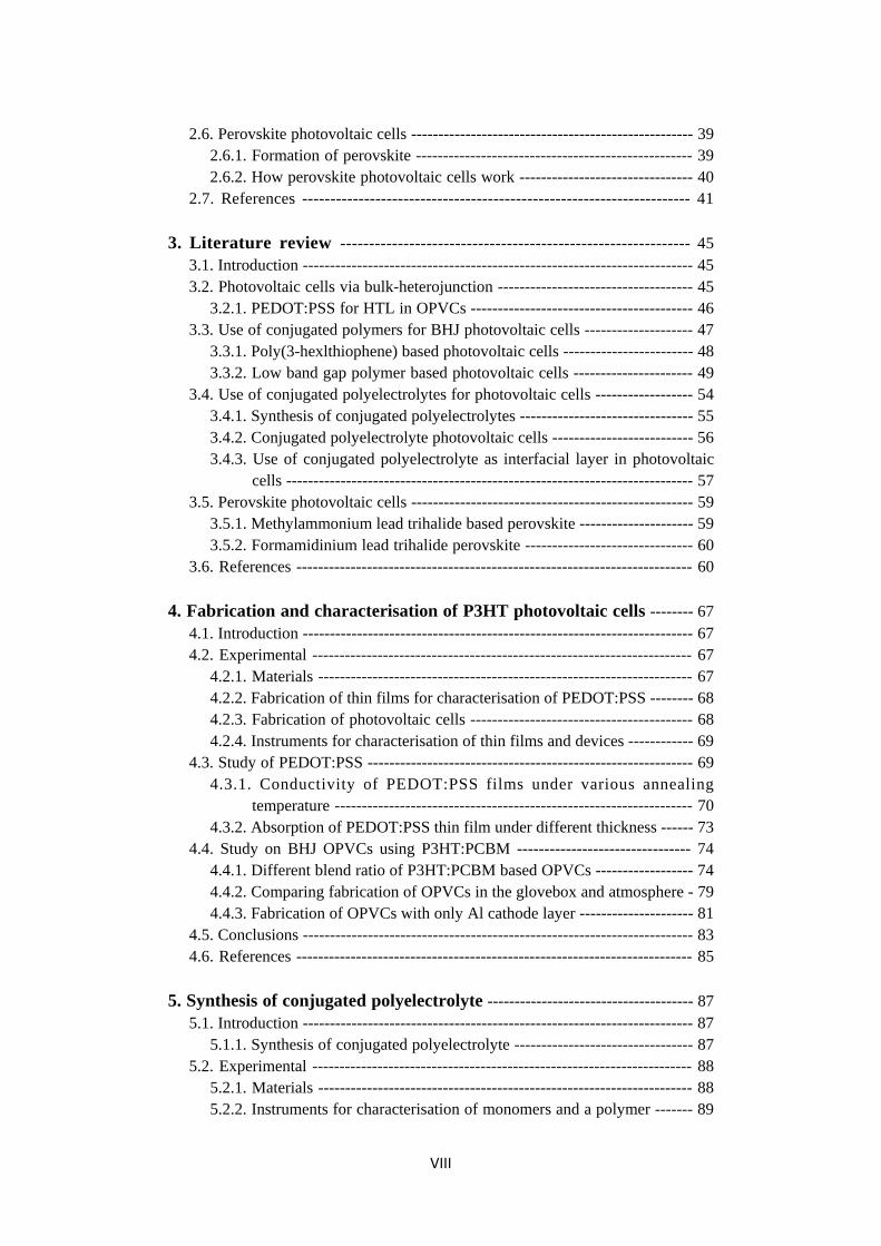
2.5. Low band gap polymers --------------------------------------------------------- 36
VII
2.6. Perovskite photovoltaic cells ---------------------------------------------------- 39 2.6.1. Formation of perovskite --------------------------------------------------- 39 2.6.2. How perovskite photovoltaic cells work -------------------------------- 40
2.7. References --------------------------------------------------------------------- 41
3. Literature review ------------------------------------------------------------- 45 3.1. Introduction ------------------------------------------------------------------------ 45 3.2. Photovoltaic cells via bulk-heterojunction ------------------------------------ 45
3.2.1. PEDOT:PSS for HTL in OPVCs ----------------------------------------- 46 3.3. Use of conjugated polymers for BHJ photovoltaic cells -------------------- 47
3.3.1. Poly(3-hexlthiophene) based photovoltaic cells ------------------------ 48 3.3.2. Low band gap polymer based photovoltaic cells ---------------------- 49
3.4. Use of conjugated polyelectrolytes for photovoltaic cells ------------------ 54 3.4.1. Synthesis of conjugated polyelectrolytes -------------------------------- 55 3.4.2. Conjugated polyelectrolyte photovoltaic cells -------------------------- 56 3.4.3. Use of conjugated polyelectrolyte as interfacial layer in photovoltaic
cells --------------------------------------------------------------------------- 57 3.5. Perovskite photovoltaic cells ---------------------------------------------------- 59
3.5.1. Methylammonium lead trihalide based perovskite --------------------- 59 3.5.2. Formamidinium lead trihalide perovskite ------------------------------- 60
3.6. References ------------------------------------------------------------------------- 60
4. Fabrication and characterisation of P3HT photovoltaic cells -------- 67 4.1. Introduction ------------------------------------------------------------------------ 67 4.2. Experimental ---------------------------------------------------------------------- 67
4.2.1. Materials --------------------------------------------------------------------- 67 4.2.2. Fabrication of thin films for characterisation of PEDOT:PSS -------- 68 4.2.3. Fabrication of photovoltaic cells ----------------------------------------- 68 4.2.4. Instruments for characterisation of thin films and devices ------------ 69
4.3. Study of PEDOT:PSS ------------------------------------------------------------ 69 4.3.1. Conductivity of PEDOT:PSS films under various annealing
temperature ------------------------------------------------------------------ 70 4.3.2. Absorption of PEDOT:PSS thin film under different thickness ------ 73
4.4. Study on BHJ OPVCs using P3HT:PCBM -------------------------------- 74 4.4.1. Different blend ratio of P3HT:PCBM based OPVCs ------------------ 74 4.4.2. Comparing fabrication of OPVCs in the glovebox and atmosphere - 79 4.4.3. Fabrication of OPVCs with only Al cathode layer --------------------- 81
4.5. Conclusions ------------------------------------------------------------------------ 83 4.6. References ------------------------------------------------------------------------- 85
5. Synthesis of conjugated polyelectrolyte -------------------------------------- 87
5.1. Introduction ------------------------------------------------------------------------ 87 5.1.1. Synthesis of conjugated polyelectrolyte --------------------------------- 87
5.2. Experimental ---------------------------------------------------------------------- 88 5.2.1. Materials --------------------------------------------------------------------- 88 5.2.2. Instruments for characterisation of monomers and a polymer ------- 89
VIII

5.2.3. Synthesis of monomers and conjugated polyelectrolyte -------------- 89 5.3. Results and discussion ----------------------------------------------------------- 94
5.3.1. NMR analysis of monomers and PSFP-DTBTP ----------------------- 94 5.3.2. FT-IR spectrum of PSFP-DTBTP --------------------------------------- 99 5.3.3. Optical properties of PSFP-DTBTP ------------------------------------ 101 5.3.4. Cyclic voltammetry measurement of PSFP-DTBTP ----------------- 103
5.4. Conclusions ---------------------------------------------------------------------- 105 5.5. References ------------------------------------------------------------------------ 105
6. Polymer photovoltaic cells with conjugated polyelectrolyte --------- 109
6.1. Introduction ---------------------------------------------------------------------- 109 6.2. Experimental --------------------------------------------------------------------- 110
6.2.1. Materials ------------------------------------------------------------------- 110 6.2.2. Organic photovoltaic cells fabrication (PSFP-DTBTP used as active
layer) ---------------------------------------------------------------- 110 6.2.3. Organic photovoltaic cells fabrication (PSFP-DTBTP used as HTL or
additive in HTL) ---------------------------------------------------------- 111 6.2.4. Preparation of films for characterisation ---------------------------- 112 6.2.5. Instruments ----------------------------------------------------------------- 112
6.3. Use PSFP-DTBTP in active layer -------------------------------------------- 113 6.3.1. Thickness change of PEDOT:PSS HTL caused by spin casting
subsequent water soluble layers ---------------------------------------- 113 6.3.2. Fabrication of water based photovoltaic cells ------------------------ 114
6.4. Use PSFP-DTBTP in HTL ----------------------------------------------------- 115 6.4.1. Optical characterisation of conjugated polyelectrolyte with
PEDOT:PSS and PCDTBT:PC71BM ----------------------------------- 116 6.4.2. FT-IR spectra of CPE and HTL layers -------------------------------- 118 6.4.3. The characterisation of band gaps of each layer ---------------------- 119 6.4.4. Work function of HTLs ------------------------------------------------- 120 6.4.5. Photovoltaic properties of devices with CPE additive in HTL ---- 120 6.4.6. Conductivity of HTLs ---------------------------------------------------- 124 6.4.7. Photoluminescence characterisation of HTL and active layer ------ 125 6.4.8. AFM characterisation of HTLs ------------------------------------------ 127 6.4.9. Photovoltaic properties of device with CPE HTL -------------------- 128
6.5. Conclusions -------------------------------------------------------------------- 130 6.6. References ------------------------------------------------------------------- 131
7. Perovskite photovoltaic cells -------------------------------------------------- 135
7.1. Introduction ------------------------------------------------------------------- 135 7.2. Experimental ------------------------------------------------------------------ 137
7.2.1. Materials -------------------------------------------------------------------- 137 7.2.2. Synthesis of methylamine iodide (MAI) ---------------------------- 137 7.2.3. Mixed perovskite precursor by various blend ratio ------------------- 137 7.2.4. Thin films fabrication for SEM, EDS, and GIWAXS ---------------- 138 7.2.5. Thin films fabrication for UV-vis absorption spectroscopy --------- 139 7.2.6. Device fabrication and characterisation ------------------------------- 139
IX

7.2.7. Instruments ---------------------------------------------------------------- 140 7.3. Results and discussion ------------------------------------------------------ 140
7.3.1. UV-vis absorption of perovskites ------------------------------------- 141 7.3.2. SEM and EDS characterisation of perovskite thin films ------------- 142 7.3.3. GIWAXS characterisation of perovskite thin films ------------------ 149 7.3.4. Photovoltaic properties of perovksite PVCs ------------------------- 153
7.4. Conclusions ---------------------------------------------------------------------- 156 7.5. References ----------------------------------------------------------------------- 157
8. Conclusions and further work ------------------------------------------------ 161
8.1. Conclusions -------------------------------------------------------------------- 161 8.2. Further work ------------------------------------------------------------------- 163
X

1. Introduction
1.1. Objectives and aims
Solar energy is a very attractive energy source because it is a stable source of
renewable energy and a sustainable fossil fuel alternative, and as such it is studied
widely (Thompson and Frechet, 2008a). The advantages of organic polymer-based
photovoltaic cells (OPVCs) and perovskite photovoltaic cells (PPVCs) are that they
offer a low cost, simple to process, light weight, mechanically flexible route to
solar cell manufacture. Furthermore, PPVCs have attracted much interest due to
their outstanding efficiency (Snaith, 2013, Sondergaard et al., 2012, Espinosa et al.,
2012, Azzopardi et al., 2011, Dennler et al., 2009, Gunes et al., 2007, Yu et al.,
1995, Facchetti, 2011, Shaheen et al., 2005, Brabec, 2004). Although, OPVCs have
the many advantages mentioned above, they still needs to improve to compare with
inorganic solar cells. The power conversion efficiency (PCE) of OPVC is about 8%
for bulk heterojunction (BHJ) solar cells based on a blend of conjugated polymer
and fullerene derivative [6,6]-phenyl-C61 butyric acid methyl ester (PCBM) (He
et al., 2011) as the active layer. In order to approach over 10% efficiency, it is
necessary to understand the fundamental active layer morphology and electronic
interaction between donor and acceptor (Scharber et al., 2006).
Reduction of organic solvent use and harmful materials in OPVCs and PPVCs are
necessary to help the environment (Capello et al., 2007, Ohlson and Hogstedt,
1981). In particular, although PPVCs showed good performance, toxicity of lead is
an issue that still need to be addressed in PPVCs (Flora et al., 2012, Landrigan,
1989). In order to reduce the effects of these harmful materials, less harmful
alternatives can be used to instead and/or the performance of the devices improved
such that less smaller areas of photovoltaic need to be manufactured.
The aim of this PhD research is the development of more sustainable PVCs
through using less harmful materials in and during the fabrication of the active
layer and/or interfacial layers in PVCs and also by increasing their efficiency. In
order to improve their sustainability the research has investigated less toxic
materials for both OPVC and PPVC.
1

In OPVCs, to reduce the use of organic solvent and harmful materials, water-
soluble conjugated polymers (known as conjugated polyelectrolytes) were
synthesised and then utilised in OPVCs. The efficiency of the OPVCs produced
were determined. Fluorene, thiophene, and benzothiadiazole groups were
introduced in the synthesis steps for the polyelectrolyte because these polymers
absorb light from 300 to 600 nm in wavelength. This project focussed on the
synthesis of suitable polymers and their subsequent characterization through
various methods (e.g. conductivity, absorption, and morphology). The main
difference between conventional conjugated polymers in OPVC and conjugated
polyelectrolytes is that it is possible to dissolve the polyelectrolytes in water.
Therefore, removing the need to produce the environmental pollutants that results
from using organic solvents. The fabrication process was optimised using
conjugated polyelectrolytes both as an active layer and as an interfacial layer.
When using it as an interfacial layer organic solvents are still needed to make the
active layer but by achieving a higher overall efficiency than previously report the
overall environmental impact of OPVCs can be reduced by increasing their
efficiency.
In PPVCs, to reduce the use of toxic materials such as lead and caesium in
perovskite, bismuth was introduced as the metal cation. Bismuth is less toxic than
lead, therefore it will reduce the use of harmful lead in perovskite. Bismuth
perovskite was applied as an active layer and its structure and morphology was
studied. Various molar ratios of bismuth perovskite precursor were applied to find
optimised molar ratio.
1.2. Origin of photovoltaic cells
Increasing energy demands and concern about climate change in the world have
focussed study on renewable, clean and abundant energy sources, of which solar
cells are a good example. The energy demands in the world are about ~1.3 × 10¹³
W, while the Earth receives ~1.2 × 10¹⁷ W of solar energy per year (Energy, 2005,
Tao, 2008). This is 10,000 times larger than the amount of energy that people use.
In particular, the Sun provides more energy to our planet in one hour, 4.3 × 10²⁰ J,
than the current worldwide annual energy consumption 4.1 × 10²⁰ J (Energy, 2005).
2

The photovoltaic effect was defined by A. E. Becquerel, a French physicist, in
1839 (Becquerel, 1839). He observed the generation of current upon illuminating
platinum electrodes covered with silver chloride in an acidic solution. The first
solid state photovoltaic cell was developed by C. Fritts, an American inventor, in
1883 (Fritts, 1883). This photovoltaic cell was made by selenium wafer with a thin
layer of gold. R. Ohl patented the modern junction semiconductor photovoltaic cell
in 1946 (Ohl, 1946) and the first silicon photovoltaic cell was realised by D.
Chapin, C. S. Fuller and G. Pearson in 1954 (Chapin et al., 1954). They worked on
silicon p–n junction photocells that reached 6% efficiency and showed significant
improvement compared to the selenium cells that measured 0.5% efficiency. The
efficiency of PVCs has improved since 1954 and it is now over 40% (NREL, 2015).
1.2.1. Photovoltaic cells based on inorganic materials
Inorganic photovoltaic cells (IPVCs) have shown good results in that they have
achieved high PCE about 46%, confirmed by the National Renewable Energy
Laboratory, due to the excellent charge carrier mobility and the environmental
stability of inorganic materials (NREL, 2015, Green et al., 2016). Since the first
photovoltaic cells were reported (1946), IPVCs have improved tremendously as
reported over the last 50 years. Various kinds of IPVCs have been discovered and
been developed such as single-crystal silicon (sc-Si) cells, polycrystalline silicon
(poly-Si) cells and heterojunction with intrinsic thin layer (HIT) cells all using
crystalline Si. Thin-film photovoltaic cell based on CdTe, copper indium gallium
diselenide (CIGS), amorphous silicon (a-Si), and microcrystalline (µc-Si) and
others have also been developed (Miles et al., 2007, Schropp et al., 2007, Slaoui
and Collins, 2007). The best research-cell efficiencies for each type and material of
photovoltaic cells are shown in Figure 1-1 reported by National Renewable Energy
Laboratory (NREL) in 2015.
The best PCE in crystalline silicon cell is from single crystalline cells, it has
approached 24.7% (non-concentrator) and 27.6% (concentrator) for about
20 years. However, the efficiency of poly-Si cells is shown to be 20.4% in
2004. The PCE of a-Si cells have gradually increased from 1976 to 2012
and it reached 13.4% (LG Electronics), while that of CIGS cells has reached
20.4% (EMPA). The advantage of poly-Si cells is that they are less
expensive to buy and manufacture. The advantage of a-Si is that they can be
3

deposited in thin films on a variety of substrates at low temperatures and the
thin film reduces the cost of an individual solar panel. Among the many
photovoltaic cells, the highest PCE photovoltaic cells are multijunction
cells. The multijunction photovoltaic cells are built up of multiple p-n
junctions using different semiconductor materials (e.g. GaAS/CIS). They
can respond to several ranges of wavelength by using different materials to
produce electric current. They have been developed PCE over 40% (Green
et al., 2016).
Figure 1-1 The best efficiencies of various kinds of photovoltaic cells (NREL, 2015).
4

The Shockley-Queisser (S-Q) limit is the maximum theoretical efficiency for
photovoltaic cells using a single p-n junction. According to the S-Q limit, the
maximum efficiency for a single junction device is around 33%, see Figure 2-29(a)
in the section 2.5. However, multijuction photovoltaic cells are able to achieve over
33% efficiency and approach up to a PCE of 86% in infinite junctions (Green,
2003).
Silicon-based PVCs lead the PVC market and dominate about 90% of the total
PVC production (SolarCellCentral.com). Even if IPVCs show good efficiencies
and account for 90%, the main drawback is their production cost due to expensive
component materials and fabrication process for the devices. Highly purified
silicon wafer is made by various steps from raw material in order to make good
efficiency of photovoltaic cells and it leads to increasing cost. Figure 1-2 shows
the steps for preparing photovoltaic cells (Saga, 2010). This is an energy intensive
and therefore expensive process (cost of polysilicon is around €15 per kilogram).
Figure 1-2 The procedure of preparing inorganic photovoltaic cells (Saga, 2010).
1.2.2. Photovoltaic cells based on organic materials
Conjugated polymer-based photovoltaic cells are becoming attractive as renewable
energy sources for energy generation due to the ability to tune their design for
efficient energy harvesting. Because conjugated polymers are generally able to
absorb a wider range of visible light by applying donor and acceptor groups in the
polymer chain whien compared to other organic materials such as monomers and
oligomers. The solid red-circles and line in Figure 1-1 indicates the PCE of a
diverse range of organic based photovoltaic cells (NREL, 2015). The best result for
organic cells was 11.1% in 2012. Although the efficiency of organic photovoltaic
5

cells has improved from 2001 to 2009, it has strikingly increased for the last 4
years, while other technologies have not been able to show this rate of
improvement in the same period. The main advantages of organic photovoltaic
cells are low-cost, flexibility, and their simple production process (Li, 2012,
Dennler et al., 2009, Thompson and Frechet, 2008b, Yu et al., 1995). Organic
materials are cheaper than inorganic materials and it is possible to process them
using diverse techniques such as solution process, spin casting, roller casting and
inkjet printing. Often several components can be deposited in one step by taking
advantage of self-organised processing. These techniques help reduce the price of
devices, decrease processing time and also make large area coating feasible.
Conjugated polymers and fullerenes are generally used as the active layer and
organic solvents such as chlorobenzene or dichlorobenzene are needed to dissolve
these materials. The solvents needed for the production of OPVCs are fairly
expensive and dangerous both environmentally and from a health and safety point
of view. In the laboratory scale, organic solvents are inevitably used for OPVCs
from a few microlitres to a few millilitres. Therefore it will be helpful to use water-
soluble or alcohol-soluble materials to reduce organic solvent use were the
production of OPVCs to be scaled up to an industrial process.
1.3. Conjugated polymers
The term ‘conjugation or conjugated’ refers to a system having connected p-
orbitals by alternating single and multiple bonds with delocalised electrons within
the molecules. Conjugated polymers have alternate p-orbitals with single and
multiple bonds and this results in their characteristic conductivity and fluorescence.
This is because electrons in p-orbitals are able to absorb energy and become
excited to higher energy state similar to the conduction band in a semiconducting
crystal and so they can cause conductivity and fluorescence. Fluorescent
conjugated polymers have attracted much interest due to their thermal stability,
strong emission properties, good process ability and wide range of potential
application as organic light emitting diodes (OLED) (Huyal et al., 2008), organic
thin film transistors (OTFT) (Li et al., 2006), organic photovoltaic cells (Staniec et
al., 2011), and chemical and biosensors (Thomas et al., 2007, Liu and Bazan,
2004a). In particular, conjugated polymers used in photovoltaic cells have drawn
much interest as renewable energy sources due to fast electron transport, low-costs,
ease of synthesis and the ability to tune their properties by altering their structure.
6

The most valuable advantage of conjugated polymers is that a many differnt
conjugated polymers can be synthesised and it is easy to change their character
(solubility, conductivity, band gap, and so on) by introducing various chemical
groups.
1.3.1. Conjugated polyelectrolytes
Conjugated polyelectrolytes (water-soluble conjugated polymers) are conjugated
polymers that contain charged side chains which give them water-solubility.
Conjugated polyelectrolytes have been synthesised with polar ionic functional
groups, such as anionic carboxylates (Kim et al., 2005), sulfonates (Vetrichelvan et
al., 2006), and cationic quaternary ammonium salts (Liu and Bazan, 2004b) within
their polymer backbones. The hydrophobic nature of conjugated polymer main
chains makes it difficult to dissolve in water because of π-π interactions between
adjacent polymer backbones causing polymer aggregations. However, by attaching
charged side chains it is possible to improve water solubility and therefore it is
possible to expand the application of conjugated polymer to various areas.
Conjugated polyelectrolytes have π-π conjugation and show photophysical
properties that are similar to conjugated polymer. However, their polarity in
solution makes polyelectrolytes show different fluorescent properties compared to
their corresponding polymer due to hydrogen bonding with solvents or reagents,
even though their polymer backbones are same. The charged side chains of
polyelectrolytes lead to aggregation with other materials. Positive-charged
conjugated polyelectrolytes can induce electrostatic assembly with negatively
charged materials. These properties allow them to be used in applications such as
biosensors for DNA and protein. Ho et al. suggested a DNA sensor using
electrostactic interaction with polythiophene and target DNA without additional
fluorophore and quencher (Ho et al., 2002). Gaylord et al. also synthesised water-
soluble conjugated poly phenylene fluorene as DNA sensors and then detected the
target DNA through FRET with fluorescein (Gaylord et al., 2002). Kwak et al.
reported protein sensor using micro-contact printing (µCP) through water-soluble
conjugated poly(para-phenylene) with fluorescein-labelled streptavidin (Kwak et
al., 2010).
From previous reports, conjugated polymers/polyelectrolytes have been used as
biosensor probe (in vitro and in vivo) (Yang et al., 2013, Li and Liu, 2012, Lee et
7

al., 2012) because conjugated polyelectrolytes show high fluorescence, good
stability and low cytotoxicity. In particular, conjugated polyelectrolytes are bio-
compatible for in vivo experiments on mice or rabbits (Ding et al., 2011). Therefore,
they are low toxicity materials and could therefore be used in photovoltaic cells as
more environmentally friendly materials than the currently used polymers.
1.3.2. Conjugated polyelectrolytes use in water for photovoltaic cells
Concern for the environment is one of the most important issues in the world. The
use of organic solvents in various fields causes health and environmental problems
(Li, 1993, Narayan et al., 2005). In particular, persistent exposure leads to
occupational diseases such as Parkinson’s disease, malignant lymphoma, and so on
(Ohlson and Hogstedt, 1981, Hardell et al., 1981). Therefore, researchers in
chemistry have tried to change from using organic solvents to using water where
possible. The advantages of water are that is has low cost, is safe, and is easy to
recycling.
For use in the OPVCs in this study, conjugated polyelectrolyte was synthesised.
The conjugated polyelectrolyte was applied as an active layer and also as a hole
transporting layer in the devices. Unfortunately, the conjugated polyelectrolyte did
not show any photovoltaic ability within the active layer. However, it showed good
ability as an additive in HTL in the devices. Although when used as an additive,
organic solvents were needed for fabrication of photovoltaic cells, water was used
as the solvent for conjugated polyelectrolyte. In addition, there was no further
organic solvent use (i.e. chlorobenzene, methanol, and so on) therefore the reported
improvement of PCE compared to previous reports (Lee et al., 2008, Li et al., 2007)
means that for the same power output less materials overall would be required,
therefore improving the environmental benefits of OPVCs.
1.4. Perovskite photovoltaic cells
1.4.1. Origin of perovskite
Perovskite was discovered in Ural Mountains by Gustav Rose in 1839 and was
named after the Russian mineralogist Lew A. Perowski. Perovskite initially denotes
calcium titanium oxide (CaTiO3), but the term perovskite is used to describe any
8

compound which has a crystal structure similar to CaTiO3 following the pioneering
synthesis of perovskite by Goldschmidt in 1926. Perovskites have the chemical
formula ABX3 structure which consists of cations, A and B, of two different sizes,
and anion X. The ideal structure of ABX3 perovskite is cubic where B cation
coordinates corner sharing (BX6) octahedral structure with anion X and A cation
neutralise total charge in 12-fold coordination. In perovskite, various divalent metal
ions are accepted for B cation (Cu, Ni, Co, Fe, Mn, Cr, Pd, Cd, Ge, Sn, Pb Eu or
Yb) (Mitzi, 1999, Liang et al., 1998, Baikie et al., 2013). Figure 1-3 shows general
perovskite structure ABX3.
Figure 1-3 The perovskite lattice structure of ABX3 (Eperon et al., 2014).
1.4.2. Organic-metal halide perovskite photovoltaic cells
As shown in Figure 1-1, the perovskite photovoltaic cells have rapidly improved
since 2010 and they have achieved over 20% PCE (Yang et al., 2015). Perovskites
are one of the most interesting materials in the photovoltaic cells field due to their
fast development and high efficiency. The first perovskite solar cell was reported
by Kojima et al. in 2009 (Kojima et al., 2009). They used methylammonium lead
halide perovskites (CH3NH3PbX3, X= Br, or/and I) as the light harvester in
sensitized solar cells. CH3NH3PbI3 or CH3NH3PbBr3 were respectively coated on
mesoporous TiO2 with liquid electrolyte between electrodes.
Advantages of perovskite photovoltaic cells are low-cost technology (Snaith, 2013),
easily tuning band gap of perovksite (Kulkarni et al., 2014), and wide range of
absorption wavelengths up to 800 nm (Eperon et al., 2014), and available versatile
structures of devices such as sensitised PPVC architecture and planar PPVC
architecture which are originated in dye-sensitised PVC and planar heterojunction
PVC respectively.
9

1.4.2.1. Sensitised perovskite photovoltaic cells
A sensitised-perovskite photovoltaic cell is a type of dye-sensitised photovoltaic
cell which includes a perovskite as the active layer and it is coated on a
mesoporous TiO2 layer. The general structure of these devices are anode/n-type
contact/TiO2:perovskite/p-type contact/cathode as shown in Figure 1-4. Sun light
is harvested by perovskite and dissociated electrons and holes are extracted by n-
type and p-type contacts respectively. Figure 1-4 shows the architecture of
sensitised perovskite photovoltaic cell (Gamliel and Etgar, 2014).
Figure 1-4 Structure of sensitised perovskite photovoltaic cell.
1.4.2.2. Planar perovskite photovoltaic cells
An interesting and remarkable feature of perovskite photovoltaic cells is that they
can also be used in planar photovoltaic architectures. The advantages of planar
architectures are that their processing is simple and the planar architecture removes
infiltration problems of the perovskite and the hole transport material into the
porous TiO2 in sensitised perovskite photovoltaic cells (Gamliel and Etgar, 2014).
This leads to less recombination and better reproducibility. The two types of
architecture of planar perovskite photovoltaic cells are shown in Figure 1-5(a) and
(b). Figure 1-5(a) shows the architecture having FTO/Metal oxide
(TiO2)/perovskite/hole transporting layer (Spiro-OMeTAD)/electrode (Au).
Dissociated electrons and holes pass through the metal oxide into the FTO and the
hole transporting layer to the electrode (Au). Another architecture of planar
10

perovskite photovoltaic cell is ITO/hole transporting layer
(PEDOT:PSS)/perovskite/electron transporting layer (PCBM)/electrode (Al). The
dissociated electrons and holes move in the opposite direction to those in the
former architecture.
Figure 1-5 The two types of planar perovksite photovoltaic cells architecture.
For PPVCs in this study, planar PPVC architecture was used. Bismuth was
replacement of lead. Bismuth is less toxic than lead due to great insolubility of
bismuth salts and it prevents their absorption (DiPalma, 2001). Bismuth-based
perovksite structure was studied in different molar ratios of methylammonium
iodide and bismuth halide.
Theory and literature related to research will be explained in the Chapter 2 and 3,
respectively. Chapter 4, 5, 6, and 7 will deal with experiment of research project.
General P3HT PVC will be explained in Chapter 4, synthesis of conjugated
polyelectrolyte and study of OPVC with conjugated polyelectrolyte will be dealt
with in the Chapter 5, and 6. In Chapter 7, bismuth-based perovskite will be
introduced.
1.5. References
AZZOPARDI, B., EMMOTT, C. J. M., URBINA, A., KREBS, F. C., MUTALE, J.
& NELSON, J. 2011. Economic assessment of solar electricity production
from organic-based photovoltaic modules in a domestic environment.
Energy & Environmental Science, 4, 3741-3753.
11

BAIKIE, T., FANG, Y., KADRO, J. M., SCHREYER, M., WEI, F.,
MHAISALKAR, S. G., GRAETZEL, M. & WHITE, T. J. 2013. Synthesis
and crystal chemistry of the hybrid perovskite (CH3NH3)PbI3 for solid-
state sensitised solar cell applications. Journal of Materials Chemistry A, 1,
5628-5641.
BECQUEREL, E. 1839. Comptes Rendus, 9, 561.
BRABEC, C. J. 2004. Organic photovoltaics: technology and market. Solar Energy
Materials and Solar Cells, 83, 273-292.
CAPELLO, C., FISCHER, U. & HUNGERBUHLER, K. 2007. What is a green
solvent? A comprehensive framework for the environmental assessment of
solvents. Green Chemistry, 9, 927-934.
CHAPIN, D. M., FULLER, C. S. & PEARSON, G. L. 1954. A New Silicon P-N
Junction Photocell for Converting Solar Radiation into Electrical Power.
Journal of Applied Physics, 25, 676-677.
DENNLER, G., SCHARBER, M. C. & BRABEC, C. J. 2009. Polymer-Fullerene
Bulk-Heterojunction Solar Cells. Advanced Materials, 21, 1323-1338.
DING, D., LI, K., ZHU, Z., PU, K. Y., HU, Y., JIANG, X. & LIU, B. 2011.
Conjugated polyelectrolyte-cisplatin complex nanoparticles for
simultaneous in vivo imaging and drug tracking. Nanoscale, 3, 1997-2002.
DIPALMA, J. R. 2001. Bismuth Toxicity, Often Mild, Can Result in Severe
Poisonings. Emergency Medicine News, 23, 16.
ENERGY, U. S. D. O. 2005. Basic Research Needs for Solar Energy Utilization.
EPERON, G. E., STRANKS, S. D., MENELAOU, C., JOHNSTON, M. B., HERZ,
L. M. & SNAITH, H. J. 2014. Formamidinium lead trihalide: a broadly
tunable perovskite for efficient planar heterojunction solar cells. Energy &
Environmental Science, 7, 982-988.
ESPINOSA, N., HOSEL, M., ANGMO, D. & KREBS, F. C. 2012. Solar cells with
one-day energy payback for the factories of the future. Energy &
Environmental Science, 5, 5117-5132.
FACCHETTI, A. 2011. pi-Conjugated Polymers for Organic Electronics and
Photovoltaic Cell Applications. Chemistry of Materials, 23, 733-758.
FLORA, G., GUPTA, D. & TIWARI, A. 2012. Toxicity of lead: A review with
recent updates. Interdiscip Toxicol, 5, 47-58.
FRITTS, C. E. 1883. On a new form of selenium cell, and some electrical
discoveries made by its use. American Journal of Science, 26, 465-472.
GAMLIEL, S. & ETGAR, L. 2014. Organo-metal perovskite based solar cells:
sensitized versus planar architecture. Rsc Advances, 4, 29012-29021.
12

GAYLORD, B. S., HEEGER, A. J. & BAZAN, G. C. 2002. DNA detection using
water-soluble conjugated polymers and peptide nucleic acid probes.
Proceedings of the National Academy of Sciences of the United States of
America, 99, 10954-10957.
GREEN, M. A. 2003. Third generation photovoltaics : advanced solar energy
conversion, Berlin ; New York, Springer.
GREEN, M. A., EMERY, K., HISHIKAWA, Y., WARTA, W. & DUNLOP, E. D.
2016. Solar cell efficiency tables (version 47). Progress in Photovoltaics,
24, 3-11.
GUNES, S., NEUGEBAUER, H. & SARICIFTCI, N. S. 2007. Conjugated
polymer-based organic solar cells. Chemical Reviews, 107, 1324-1338.
HARDELL, L., ERIKSSON, M., LENNER, P. & LUNDGREN, E. 1981.
Malignant lymphoma and exposure to chemicals, especially organic
solvents, chlorophenols and phenoxy acids: a case-control study. Br J
Cancer, 43, 169-76.
HE, Z. C., ZHONG, C. M., HUANG, X., WONG, W. Y., WU, H. B., CHEN, L.
W., SU, S. J. & CAO, Y. 2011. Simultaneous Enhancement of Open-
Circuit Voltage, Short-Circuit Current Density, and Fill Factor in Polymer
Solar Cells. Advanced Materials, 23, 4636-+.
HO, H. A., BOISSINOT, M., BERGERON, M. G., CORBEIL, G., DORE, K.,
BOUDREAU, D. & LECLERC, M. 2002. Colorimetric and fluorometric
detection of nucleic acids using cationic polythiophene derivatives.
Angewandte Chemie-International Edition, 41, 1548-1551.
HUYAL, I. O., KOLDEMIR, U., OZEL, T., DEMIR, H. V. & TUNCEL, D. 2008.
On the origin of high quality white light emission from a hybrid
organic/inorganic light emitting diode using azide functionalized
polyfluorene. Journal of Materials Chemistry, 18, 3568-3574.
KIM, I. B., DUNKHORST, A. & BUNZ, U. H. F. 2005. Nonspecific interactions
of a carboxylate-substituted PPE with proteins. A cautionary tale for
biosensor applications. Langmuir, 21, 7985-7989.
KOJIMA, A., TESHIMA, K., SHIRAI, Y. & MIYASAKA, T. 2009. Organometal
Halide Perovskites as Visible-Light Sensitizers for Photovoltaic Cells.
Journal of the American Chemical Society, 131, 6050-+.
KULKARNI, S. A., BAIKIE, T., BOIX, P. P., YANTARA, N., MATHEWS, N. &
MHAISALKAR, S. 2014. Band-gap tuning of lead halide perovskites
using a sequential deposition process. Journal of Materials Chemistry A, 2,
9221-9225.
13

KWAK, C. K., KIM, D. G., KIM, T. H., LEE, C. S., LEE, M. & LEE, T. S. 2010.
Simultaneous and Dual Emissive Imaging by Micro-Contact Printing on
the Surface of Electrostatically Assembled Water-Soluble Poly(p-
phenylene) Using FRET. Advanced Functional Materials, 20, 3847-3855.
LANDRIGAN, P. J. 1989. Toxicity of Lead at Low-Dose. British Journal of
Industrial Medicine, 46, 593-596.
LEE, J. K., MA, W. L., BRABEC, C. J., YUEN, J., MOON, J. S., KIM, J. Y., LEE,
K., BAZAN, G. C. & HEEGER, A. J. 2008. Processing additives for
improved efficiency from bulk heterojunction solar cells. Journal of the
American Chemical Society, 130, 3619-3623.
LEE, K., LEE, J., JEONG, E. J., KRONK, A., ELENITOBA-JOHNSON, K. S.,
LIM, M. S. & KIM, J. 2012. Conjugated polyelectrolyte-antibody hybrid
materials for highly fluorescent live cell-imaging. Adv Mater, 24, 2479-84.
LI, C. J. 1993. Organic-Reactions in Aqueous-Media - with a Focus on Carbon-
Carbon Bond Formation. Chemical Reviews, 93, 2023-2035.
LI, G., YAO, Y., YANG, H., SHROTRIYA, V., YANG, G. & YANG, Y. 2007.
"Solvent annealing" effect in polymer solar cells based on poly(3-
hexylthiophene) and methanofullerenes. Advanced Functional Materials,
17, 1636-1644.
LI, K. & LIU, B. 2012. Polymer encapsulated conjugated polymer nanoparticles
for fluorescence bioimaging. Journal of Materials Chemistry, 22, 1257-
1264.
LI, Y. F. 2012. Molecular Design of Photovoltaic Materials for Polymer Solar
Cells: Toward Suitable Electronic Energy Levels and Broad Absorption.
Accounts of Chemical Research, 45, 723-733.
LI, Y. N., WU, Y. L. & ONG, B. S. 2006. Polyindolo[3,2-b]carbazoles: A new
class of p-channel semiconductor polymers for organic thin-film transistors.
Macromolecules, 39, 6521-6527.
LIANG, K., MITZI, D. B. & PRIKAS, M. T. 1998. Synthesis and Characterization
of Organic−Inorganic Perovskite Thin Films Prepared Using a Versatile
Two-Step Dipping Technique. Chemistry of Materials, 10, 403-411.
LIU, B. & BAZAN, G. C. 2004a. Homogeneous fluorescence-based DNA
detection with water-soluble conjugated polymers. Chemistry of Materials,
16, 4467-4476.
LIU, B. & BAZAN, G. C. 2004b. Interpolyelectrolyte complexes of conjugated
copolymers and DNA: Platforms for multicolor biosensors. Journal of the
American Chemical Society, 126, 1942-1943.
14

MILES, R. W., ZOPPI, G. & FORBES, I. 2007. Inorganic photovoltaic cells.
Materials Today, 10, 20-27.
MITZI, D. B. 1999. Synthesis, Structure, and Properties of Organic-Inorganic
Perovskites and Related Materials. Progress in Inorganic Chemistry. John
Wiley & Sons, Inc.
NARAYAN, S., MULDOON, J., FINN, M. G., FOKIN, V. V., KOLB, H. C. &
SHARPLESS, K. B. 2005. "On water": Unique reactivity of organic
compounds in aqueous suspension. Angewandte Chemie-International
Edition, 44, 3275-3279.
NREL. 2015. http://www.nrel.gov/ncpv/images/efficiency_chart.jpg [Online].
National Renewable Energy Laboratory. Available:
http://www.nrel.gov/ncpv/images/efficiency_chart.jpg.
OHL, R. 1946. LIGHT-SENSITIVE ELECTRIC DEVICE Filed.
OHLSON, C. G. & HOGSTEDT, C. 1981. Parkinson's disease and occupational
exposure to organic solvents, agricultural chemicals and mercury--a case-
referent study. Scand J Work Environ Health, 7, 252-6.
SAGA, T. 2010. Advances in crystalline silicon solar cell technology for industrial
mass production. Npg Asia Materials, 2, 96-102.
SCHARBER, M. C., WUHLBACHER, D., KOPPE, M., DENK, P., WALDAUF,
C., HEEGER, A. J. & BRABEC, C. L. 2006. Design rules for donors in
bulk-heterojunction solar cells - Towards 10 % energy-conversion
efficiency. Advanced Materials, 18, 789-+.
SCHROPP, R. E. I., CARIUS, R. & BEAUCARNE, G. 2007. Amorphous silicon,
microcrystalline silicon, and thin-film polycrystalline silicon solar cells.
Mrs Bulletin, 32, 219-224.
SHAHEEN, S. E., GINLEY, D. S. & JABBOUR, G. E. 2005. Organic-based
photovoltaics. toward low-cost power generation. Mrs Bulletin, 30, 10-19.
SLAOUI, A. & COLLINS, R. T. 2007. Advanced inorganic materials for
photovoltaics. Mrs Bulletin, 32, 211-218.
SNAITH, H. J. 2013. Perovskites: The Emergence of a New Era for Low-Cost,
High-Efficiency Solar Cells. Journal of Physical Chemistry Letters, 4,
3623-3630.
SOLARCELLCENTRAL.COM. http://solarcellcentral.com/index.html [Online].
Available: http://solarcellcentral.com/index.html.
SONDERGAARD, R., HOSEL, M., ANGMO, D., LARSEN-OLSEN, T. T. &
KREBS, F. C. 2012. Roll-to-roll fabrication of polymer solar cells.
Materials Today, 15, 36-49.
15

STANIEC, P. A., PARNELL, A. J., DUNBAR, A. D. F., YI, H. N., PEARSON, A.
J., WANG, T., HOPKINSON, P. E., KINANE, C., DALGLIESH, R. M.,
DONALD, A. M., RYAN, A. J., IRAQI, A., JONES, R. A. L. & LIDZEY,
D. G. 2011. The Nanoscale Morphology of a PCDTBT: PCBM
Photovoltaic Blend. Advanced Energy Materials, 1, 499-504.
TAO, M. 2008. Inorganic Photovoltaic Solar Cells: Silicon and Beyond. The
Electrochemical Society Interface, 30.
THOMAS, S. W., JOLY, G. D. & SWAGER, T. M. 2007. Chemical sensors based
on amplifying fluorescent conjugated polymers. Chemical Reviews, 107,
1339-1386.
THOMPSON, B. C. & FRECHET, J. M. 2008a. Polymer-fullerene composite solar
cells. Angew Chem Int Ed Engl, 47, 58-77.
THOMPSON, B. C. & FRECHET, J. M. J. 2008b. Organic photovoltaics -
Polymer-fullerene composite solar cells. Angewandte Chemie-
International Edition, 47, 58-77.
VETRICHELVAN, M., LI, H. R., RAVINDRANATH, R. & VALIYAVEETTIL,
S. 2006. Synthesis and comparison of the structure-property relationships
of symmetric and asymmetric water-soluble poly(p-phenylene)s. Journal
of Polymer Science Part a-Polymer Chemistry, 44, 3763-3777.
YANG, G., LIU, L., LV, F. & WANG, S. 2013. Conjugated polyelectrolyte
materials for promoting progenitor cell growth without serum. Sci Rep, 3,
1702.
YANG, W. S., NOH, J. H., JEON, N. J., KIM, Y. C., RYU, S., SEO, J. & SEOK, S.
I. 2015. High-performance photovoltaic perovskite layers fabricated
through intramolecular exchange. Science, 348, 1234-1237.
YU, G., GAO, J., HUMMELEN, J. C., WUDL, F. & HEEGER, A. J. 1995.
Polymer Photovoltaic Cells - Enhanced Efficiencies Via a Network of
Internal Donor-Acceptor Heterojunctions. Science, 270, 1789-1791.
16

2. Theory
2.1. Synthesis
Some of the synthesis methods and theories described here for the study of
synthesis of conjugated polyelectrolyte are taken from the texts Organic Chemistry
(Klein, 2015, Clayden et al., 2012, McMurry, 1996) and Design and Synthesis of
Conjugated Polymers (Leclerc and Morin, 2010).
Synthesis is an important part of the research process to achieve better results from
photovoltaic cells using low band gap polymers. In order to synthesise low band
gap conjugated polyelectrolytes in this study, which are able to absorb sunlight at
long wavelengths (around 600 nm), an electrophilic substitution reaction, sultone
ring open reaction, and Suzki-Miyaura cross coupling (polymerisation) using
palladium catalyst were used.
2.1.1. Electrophilic aromatic substitution (for bromination)
Electrophilic aromatic substitution is a significant reaction for aromatic compounds
because functional side groups such as halogen, alkyl, sulfonyl, nitryl and acyl
groups can be attached to conjugated polymer backbone using electrophilic
aromatic substitution.
Before dealing with electrophilic aromatic reactions, the term aromatic is briefly
explained. In general aromatic means materials which have scent and chemically
aromatic refers to chemicals which have conjugated structures similar to benzene
present. Benzene is a symmetrical planar hexagon having six carbons (sp2) and six
hydrogens (Hückel’s 4n + 2 rule). Therefore, a benzene ring forms conjugation as
explained in Chapter 1. A remarkable feature of benzene is that all the carbon
bond lengths are 139 pm which falls between the single bond (154 pm) and double
bond (134 pm) lengths. The structure of benzene is illustrated in Figure 2-1.
Alternating single and double bonds of benzene structure was firstly suggested by
German chemist Friedrich August Kekulé in 1865 (Kekuié, 1866, Kekulé, 1872).
17

Figure 2-1 Structure of benzene (Clayden et al., 2012, Kekulé, 1872, Kekuié, 1866).
Alternating double and single bonds make the electrons delocalise in the materials,
therefore benzene is stabilised by conjugation. Benzene stability is higher than
expected and this is proven by the energy of hydrogenation of benzene.
Hydrogenation is the addition of hydrogen to materials. Figure 2-2 shows energy
diagram of hydrogenation heats for cyclohexene, 1,3-cyclohexadiene, and benzene.
Hydrogenation heat of an unsaturated compound is the most direct way to measure
its resonance energy (Rogers and Mclaffer.Fj, 1971). Cyclohexene has one double
bond (CH2=CH2). The double bond is changed to a single bond during
hydrogenation and the enthalpy is changed during the reaction. The enthalpy
change of this reaction by hydrogen is -120 kJ/mol. From this enthalpy change, the
hydrogenation heat of 1,3-cyclohexadiene was expected to be -240 kJ/mol. The
observed hydrogenation heat of 1,3-cyclohexadiene was -232 kJ/mol and it was not
very different from the expected value (Clayden et al., 2012, McMurry, 1996). As
shown in Figure 2-2, however, the expected hydrogenation heat of benzene is -360
kJ/mol, but the actual heat of hydrogenation is -208 kJ/mol. The energy difference
(152 kJ/mol) between the expected value and the actual value is called the
stabilisation energy of benzene and this value is associated with aromaticity.
Figure 2-2 Energy diagram of hydrogenation heats for cyclohexene, 1,3-cyclohexadiene,
and benzene (Klein, 2015).
18

Table 2-1 summarises the expected and observed hydrogenation heats of
cyclohexene, 1,3-cyclohexadiene, and benzene.
Table 2-1 Hydrogenation heats of cyclohexene, 1,3-cyclohexadiene, and benzene
materials Expected
hydrogenation heats
Observed
hydrogenation heats
Cyclohexene -120 kJ/mol -120 kJ/mol
1,3-cyclohexadiene -240 kJ/mol -232 kJ/mol
Benzene -360 kJ/mol -208 kJ/mol
A benzene ring has a high electron density due to its six π electrons. Therefore,
benzene reacts as an electron donor to electrophilic materials (electron acceptor)
during electrophilic aromatic substitution. In order to understand electrophilic
aromatic substitution, this reaction is compared with an electrophilic addition
reaction. Alkenes react easily with electrophiles such as hydrochloric acid (HCl) or
bromine (Br2) and the alkane is produced by an additional reaction. If HCl is added
into the alkene, the electrophile H+ combines with a carbon which is double bonded
and the other carbon becomes a carbocation. Then the Cl- ion attacks the
carbocation.
When Br2 is added into the cyclohexene, trans-1,2-dibromo-cyclohexane is
produced. The reaction mechanism is same with HCl additional reaction above
mentioned and it is rapidly processed. When Br2 is added into the benzene,
hydrogen is replaced by bromine. However, a Lewis acid catalyst such as FeBr3 or
AlCl3 is needed in order for the electrophilic aromatic substitution to occur.
Because the reactivity of benzene is lower than the alkene due to the stability of its
aromatic ring. The mechanism of both electrophilic addition and electrophilic
substitution is illustrated in Figure 2-3.
Figure 2-3 The mechanism of electrophilic addtion on cycloalkene and electrophilic
substitution on benzene (Clayden et al., 2012).
19

As shown in Figure 2-3 the catalyst, AlCl3 or FeBr3, makes a complex with Br2, so
the electrophilicity of complexed Br2 is increased compared to Br2 and it acts like
Br+ in electrophilic substitution. Then the π electrons of the benzene attack the
polarised bromine and it forms an intermediate carbocation. In contrast with
electrophilic addition, H+ is eliminated from the benzene intermediate carbocation
and it forms an aromatic (benzene) ring again in order to preserve delocalisation
and stability in electrophilic substitution. The mechanism and energy diagram of
electrophilic aromatic substitution is shown in Figure 2-4.
Figure 2-4 Energy diagram of electrophilic substituted bromination of benzene (McMurry,
1996).
2.1.2. Nucleophilic substitution (for fluorene and sultone reaction)
Polyfluorene (fluorene) is a polycyclic aromatic hydrocarbon. Polyfluorene
(fluorene) is obtained from coal tar and discovered by M. Berthelot in 1883 (W. R.
Hodgkinson, 1883). A term ‘fluorene’ is related to its fluorescence. Because of this
blue fluorescence, fluorene has been applied in various fields such as
electroluminescence devices (Jiang et al., 2000), and photovoltaic cells (Yohannes
et al., 2004). Figure 2-5 shows fluorene.
Figure 2-5 The structure of fluorene.
20

Sultone is any heterocyclic ester of the hydroxy sulfonic acids. It is similar to
lactone. The term of sultone and structure was first introduced in 1888 by H.
Erdmann to explain the aromatic ring including hydroxyl sulfonic acid, 1,8-
naphthosultone (Erdmann, 1888, Mondal, 2012) in Figure 2-6.
O S OO
Figure 2-6 The structure of 1,8-naphthosultone.
Sultone is an interesting heterocyclic compound which permits the attachment of
alkyl chains accompanying the sulfonic acid groups. In this research, sulfoalkyl
groups from sultone were introduced to enhance water-solubility of conjugated
polymer.
Sultone and fluorene reaction is based on nucelophilic substitution and product was
2,7-dibromo-9,9-bis(4-sulfonatobutyl)fluorene disodium in the research. Therefore,
in this part, nucleophilic substitution will be mentioned. Nucleophilic substitution
is a fundamental technique in organic synthesis. Figure 2-7 shows the structure of
2,7-dibromo-9,9-bis(4-sulfonatobutyl)fluorene disodium.
Br Br
NaO3S SO3Na Figure 2-7 The structure of 2,7-dibromo-9,9-bis(4-sulfonatobutyl)fluorene disodium
In this chapter, the mechanism of nucleophilic substitution will be explained.
Nucleophilic substitution (SN) is the reaction where one group is replaced by a
nucleophile. In general, SN is easily achieved with alkyl halide because the carbon
linked to the halogen is slightly positively charged due to electronegativity of
halogen. In Figure 2-8, a nucleophile attacks the positive carbon and the halogen is
replaced by the nucleophile.
21

SSNN22HOHO MeMe II HOHO MeMe II
Figure 2-8 The mechanism of SN2 reaction with methyl iodide and hydroxide (Clayden et
al., 2012).
In Figure 2-8, the reaction rate is determined by the concentration of OH- and MeI.
In other words, if the amounts of reactant or nucleophile are increased, their
reaction is rapidly processed. This SN reaction mechanism was suggested by E. D.
Hugh, and C. Ingold in 1937 and it explains both the reaction rate and
stereochemistry. This reaction is named an SN2 reaction because it is a substitution
reaction which is, nucleophilic, and bimolecular.
The most important feature of SN2 reactions are that the reaction progressed in one
step and it is affected by steric hindrance. As shown in Figure 2-9, the new
bonding with an incoming nucleophile is produced and another bonding is cleaved
in same time. The incoming nucleophile attacks the carbon on the opposite side to
that linked with the halide (electron withdrawing group or leaving group) and then
it enters the transition state. In a transition state, carbon and three substituents are
in a planar arrangement. The nucleophile is connected with the carbon and the
halide group is disconnected.
Figure 2-9 The mechanism of SN2 reaction. The nucleophile attacks carbon through 180°
oppoite directioin of leaving group (McMurry, 1996).
Steric effects (hindrance) are important factors in deciding whether a reaction is
SN2 or SN1. In SN2 reactions, since the incoming nucleophile has partial bond
formation with the alkyl halide in transition state, it is sensible that a hindered,
bulky substrate should prevent easy approach of the nucleophile, making bond
formation difficult. Figure 2-10 shows steric hindrance to the SN2 reaction.
22

Figure 2-10 Steric hindrance of SN2 reaction. (a) bromomethane has the fastest SN2
reaction rate, the reaction rates of (b) bromoethane, (c) bromopropane (secondary), and (d)
2-bromo-2-methylpropane (tertiary) are gradually reduced due to steric hindrance
(McMurry, 1996).
Figure 2-11 The mechanism of SN1 reaction (Clayden et al., 2012).
Another nucleophilic substitution mechanism is illustrated in Figure 2-11. This
nucleophilic substitution is processed by two steps. There is loss of halogen
(leaving) group and it forms an intermediate carbocation and then the nucleophile
attacks the intermediate carbocation. In the reaction, reaction rate is only
determined by concentration of the reactant. Therefore, the reaction is named as
SN1 from substitution, nucleophilic, and unimolecular. The main difference with an
SN2 reaction is that SN1 reaction is a stepwise process due to steric hindrance. As a
result, SN1 reaction produces a racemic mixture and it is described in Figure 2-12.
Figure 2-12 Stereochemistry of SN1. This reaction produces racemic structure via
carbocation intermediate (McMurry, 1996).
23

In the reaction, tertiary alkyl halides react most quickly, but methyl and primary
alkyl halide are unreactive via SN1. Tertiary alkyl halides show the fastest reaction
because a nucleophile is not directly attacking the reactant due to steric hindrance.
Therefore, the leaving group is cleaved first; then the resulting intermediate
carbocation reacts with a nucleophile.
Figure 2-13 The stability of methyl, primary, secondary, and tertiary carbocation (Klein,
2015).
In the SN1 reaction, the dominant factor is the stability of the carbocation. Figure
2-13 shows the stability of the carbocations. As shown in Figure 2-13, the
carbocations are stabilised by neighboring alkyl groups. Formation of tertiary
carbocation is more stable and faster than other carbocation in SN1 reactions.
2.1.3. Suzuki-Miyaura cross coupling
Conjugated polymers can be directly or indirectly connected by conjugation of
aromatic units or double or triple bonds. In order to synthesise the conjugated
polymer, several synthesis techniques are used such as Stille, Sonogashira, Heck,
Suzuki-Miyaura cross coupling and so on. The common feature of these coupling
reactions is using palladium (Pd) catalyst. Among many cross coupling reactions
using Pd catalyst, Suzuki-Miyaura cross coupling is frequently used for synthesis
of aromatic-aromatic single bond reactions. In this research, Suzuki-Miyaura cross
coupling was used for synthesis of a conjugated polyelectrolyte.
Suzuki-Miyaura cross coupling was first invented by Suzuki, Miyaura, and
colleagues in 1979. It allows the connection of two specific sp2-hybridized C atoms
more efficiently and under milder conditions. It has been used worldwide for a few
decades and it is often simply called “Suzuki coupling”.
24

Figure 2-14 The two different types (a) XX/BB and (b) XB approaches to Suzuki coupling.
X is halogen group such as Br, Cl, and I, but Br is commonly used (Leclerc and Morin,
2010). X is halogen and B is boronic acid.
Suzuki coupling is the reaction in which aryl halides and organoboronic acids are
reacted in the presence of Pd catalyst. Although lots of conditions for Suzuki
coupling such as solvents, catalysts, and bases are important, in this chapter, the
reaction mechanism will be dealt with. This is stepwise growth type reaction and
the chemical equation is illustrated in Figure 2-14.
As shown in Figure 2-14, it is possible to approach with two types of XX/BB and
XB. X and B are functional groups in the monomer including boronic acid and
halogen, respectively. XX/BB type needs two different materials aryl halide and
aryl boronic acid resulting in polyarylene backbone. The polyarylene made by
AA/BB type is an alternating polymer and it allows that various aromatic groups
are applied. However, AB type is only making one kind of repeating unit.
25

Figure 2-15 Suzuki Coupling full mechanism with NaOtBu (Leclerc and Morin, 2010).
The mechanism of Suzuki coupling is shown in Figure 2-15. The first step is that
Pd catalyst is oxidative addition to halide then it forms the R2-Pd-X formation (3).
The halide is replaced by NaOtBu and R2-Pd-OtBu intermediate (4) is formed.
Boron part is changed by NaOtBu to R1-BY2-OtBu (6). (4) is transmetalated with (6)
and it forms R1-Pd-R2 (8). Pd catalyst is restored by reductive elimination and (8) is
changed to R1-R2. The Suzuki coupling was applied to final step of synthesis for
conjugated polyelectrolyte in the research and the procedure of synthesis is
described in Chapter 5.
2.2 Photovoltaic cell
In this section, the basic principles of photovoltaic cells are described and general
fabrication mechanisms are explained. The various theories are taken from
textbooks (Nelson, 2003, Wenham, 2007).
2. 2. 1. Solar radiation
In order to find suitable polymers and achieve good efficiency for PVCs,
understanding solar radiation is an important factor. Even if solar radiation is
26

constant, the radiation which reaches the Earth’s surface is altered due to
atmospheric effects such as absorption and scattering. The atmospheric effects may
cause reduction of the incident light available to terrestrial PVCs. Figure 2-16
shows the spectra of the solar radiation of outside the atmosphere (AM 0), and the
Earth’s surface (AM 1.5) (NREL).
0 1000 20000
1
2
Sunl
ight
Inte
nsity
(kW
/m2 /µ
m)
Wavelength (nm)
AM 0 AM 1.5
Figure 2-16 The solar radiation of outside the atmosphere (AM 0, red), and the Earth’s
surface (AM 1.5, blue) (NREL).
According to the blue line (AM 1.5) in Figure 2-16, the solar radiation has been
absorbed and scattered by O3, O2, H2O, and CO2 as well as air molecules and dust
in the atmosphere. These factors cause significant reduction in the sunlight
intensity. As shown in Figure 2-16, sunlight intensity is reduced in the atmosphere,
however lots of photons still reach the surface of the Earth at around 0.5 µm.
Therefore when materials can absorb light at around 0.5 µm, they can capture more
of the available photons and convert them to current.
The term Air Mass (AM) refers to the direct path length which the sunlight must
pass through the atmosphere on way to reach the Earth’s surface when the sun is
vertically upwards. The equation of AM is defined as:
AM = 1cosθ
(2.1)
27

The AM relies on the angle of the sun. When θ is zero from overhead, AM equals 1.
AM 1.5 (θ is 48.2° from overhead) and is used as the standard sunlight spectrum
for photovoltaic cell testing. In order to achieve a standard test of photovoltaic
cells, standard test conditions have been specified. They are a cell temperature of
25 °C and an irradiance of 1000 W/m2 with an AM 1.5 spectrum. These correspond
to the irradiance and spectrum of incident sunlight on a clear day with the sun at an
angle of 41.8° above the horizon, which is a reasonable approximation for the
average insolation at mid lattitudes.
Figure 2-17 The Air Mass through which radiation must pass before striking the Earth's
surface (Wenham et al., 2007).
2.3. Theory of I-V characterisation in photovoltaic cells
2.3.1. The effect of light
Photovoltaic cells have been designed as a current source and to generate current
when they absorb incident light, while photovoltaic cells acts like a diode when
they are in the dark (Wenham, 2007, Nelson, 2003). Therefore, photovoltaic cells
in the dark can be described using the ideal diode law below (2.2):
I = I0 �exp �𝑞𝑉𝑘𝑇� − 1� (2.2)
Where I is current, I0 is the saturation current (leakage current of the diode when
there is no light), V is measured voltage, q is electric charge (1.6 X 10⁻¹⁹
28

Coulombs), k is Boltzmann constant (1.38 X 10⁻²³ J/K), and T is the temperature in
Kelvin. Figure 2-18 shows I-V curve of photovoltaic cells as a diode in dark.
Figure 2-18 The I-V curve of photovoltaic cells in dark.
However, when photovoltaic cells absorb the incident light, the light effect is added
to the diode law. According to the equation (2.3):
I = I0 �exp � 𝑞𝑉𝑛𝑘𝑇
� − 1� − IL (2.3)
Where IL is light generated current, and n is ideal factor (1<n<2). As showing
Figure 2-19, absorbed light shifts the I-V curve down into fourth quadrant.
Figure 2-19 The I-V curve of photovoltaic cells toward effect of incident light.
29

2.3.2. Short circuit current (ISC) and open circuit voltage (VOC)
The equation (2.3) for the I-V curve in light can be re-defined so the direction of
current flow is opposite such that the current produced is positive rather than
negative and it can be written in first quadrant as shown below in equation (2.4):
I = IL − I0 �exp � 𝑞𝑉𝑛𝑘𝑇
� − 1� (2.4)
According to the equation (2.4), Figure 2-20 shows I-V curve in first quadrant and
ISC and VOC are described in the section below.
Figure 2-20 The I-V curve of photovoltaic cells in light (first quadrant).
The short circuit current (ISC) is defined as the maximum current when the voltage
across the photovoltaic cell equals 0. For an ideal cell, current value (ISC) equals IL
when V=0. ISC value relates to the number of photons captured as the area of the
photovoltaic cell is increased. To reduce any effects due to different the cell areas
and allow comparison between cells, short circuit current density (JSC = ISC/area
(mA/cm2)) is more useful than ISC.
The open circuit voltage (VOC) is defined as the maximum voltage on a cell when
no current flows. VOC corresponds to the amount of voltage across the solar cell
when no current is flowing in the solar cell in sunlight. VOC is determined by the
difference between the HOMO of the donor and LUMO of the acceptor
components (Brabec et al., 2001).
30

2.3.3. Maximum power (Pmp), maximum current (Imp), and maximum voltage
(Vmp)
Figure 2-21 Maximum power in I-V curve of photovoltaic cells.
The power of the photovoltaic cells is characterised by the equation P = IV. The
maximum power point is shown in Figure 2-21. According to the equation, the
theoretical maximum power (Pmp) is the product of ISC and VOC when they have
ideal conditions but it is not realistic due to resistivity in the devices. However,
maximum power is generally the multiplication of some value for Vmp between
zero and VOC on the V-axis and another for Imp between zero and ISC on the I-axis.
The maximum value of current and voltage at the Pmp are represented as Vmp and
Imp respectively.
2.3.4. Fill factor
The quality of the solar cell is evaluated by fill factor (FF). FF is the ratio of
maximum power output (Imp, Vmp green rectangle) to theoretical power output (ISC,
VOC pink rectangle). The equation (2.5) and area of ratio are depicted below:
FF = Pmp
PT= ImpVmp
IscVoc (2.5)
31

Figure 2-22 The areas for calculation of FF (FF is the green region over pink region).
The quality of solar cells develops when FF is closer to 1.
2.3.5. The effects of parasitic (series and shunt) resistances
In general solar cells have parasitic resistances known as series (Rs) and shunt (Rsh).
A simplified equivalent circuit for a photovoltaic cell is described in Figure 2-23
and also the equation included resistances is shown below (2.6).
I = IL − I0 �exp� V+IRs�nkT q� �
� − 1� − V+IRsRsh
(2.6)
Figure 2-23 Simplified equivalent circuit of a photovoltaic cell.
These two resistances cause reduction of the FF and the efficiency of solar cells.
The main reason of series resistance is from bulk resistance which is from resistive
contacts, carrier mobility through front surface to the contacts, and the resistance of
semiconductor to metal current flow. The effect of series resistance is illustrated in
Figure 2-24. According to the Figure 2-24 and equation ∆V=IRs, medium Rs
makes V is decreased, while large Rs causes ISC to fall down.
32

Figure 2-24 The I-V curve from the effect of series resistance.
The main causes of shunt resistance are due to leakage across the p-n junction and
impurities in the junction region like the edge of the cell. The effect of shunt
resistance is shown by Figure 2-25. In Figure 2-25, if Rsh is largely decreased, VOC
will decline.
Figure 2-25 The I-V curve from the effect of shunt resistance.
2.3.6. Power conversion efficiency (PCE, η) of photovoltaic cells
The PCE of photovoltaic cell is the ratio of power output from the solar cell to
power input from the sun. The efficiency is considerably influenced by the
spectrum and intensity of the sunlight and temperature. Therefore, the performance
of solar cells must be measured in same condition to compare to other cells. The
photovoltaic cells on the Earth are measured under AM 1.5 conditions (light output
from solar simulator is 100 mW/cm2) and at 25°C. The equation of efficiency is
defined as (2.7):
33

η = PoutPin
≅ PmaxPin
= VOCISCFFPin
(2.7)
Where, Pout is Pmax when the cell can be worked up to its maximum power output to
get maximum efficiency. In this section, general principles of which apply to all
photovoltaic cells have been explained so far, but in the next section, the operation
mechanism of BHJ in OPVCs and PPVCs will be explained because these are the
device types used for this project.
2.4. Organic bulk-heterojunction (BHJ) photovoltaic cells
2.4.1. The operation of organic BHJ photovoltaic cells
A solar cell or photovoltaic cell is a device which absorbs light and then converts
the energy from light to electricity by charge separation and transport (Thompson
and Frechet, 2008a). Absorbed light generates excitons (bound state of an electron
and an electron hole) that can dissociate to form electrons and holes. The electrons
from the highest occupied molecular orbital (HOMO, valence band) are excited to
the lowest unoccupied molecular orbital (LUMO, conduction band) and quickly
relax upon illumination in the active layer. In order to generate a photocurrent the
electrons and holes need to be separated from the active layer and transferred to the
front contact and rear contact (e.g. metal layer and ITO layer), along percolating
pathways, respectively. Figure 2-26 shows the band structure of organic BHJ cells.
A BHJ active layer has an interpenetrating nanostructure of donor and acceptor
materials and this means that electrons and holes are easily dissociated.
Figure 2-26 The energy structure of an organic bulk-heterojunction cells.
34

2.4.2. How BHJ photovoltaic cells work
To date, OPVCs have shown lower PCE than that of IPVCs. Therefore, increasing
PCE of OPVCs is an important issue to achieve effective conversion of solar
energy into electricity and to replace IPVCs in industry, and also to improve their
environmental sustainability. Bulk-heterojunction (BHJ) solar cells based on
conjugated polymer are a promising technology to improve PCE of OPVCs.
Figure 2-27 The architecture of bulk-heterojunction photovoltaic cell.
The active layers in BHJ solar cells consist of mixtures of a polymer donor and
acceptor. The two components in the active layer of a BHJ form an interpenetrating
network which provides nanostructure and offers a large interfacial area for
efficient exciton dissociation. This nanostructure of BHJ is important because
exciton diffusion lengths of organic polymers are only a few nanometres (Tamai et
al., 2015). The active layer polymer absorbs the incident light and then electrons
are excited to conduction band then dissociated electrons move to metal cathode
through PCBM; and holes move to ITO through PEDOT:PSS. PEDOT:PSS gives
photovoltaic cells positive effects that PEDOT:PSS block the electron from active
layer to ITO because it has higher LUMO level than materials in active layer and
improve smoothness of the ITO contact (Arias et al., 1999, Kim et al., 2009).
Conjugated polymers (Liang et al., 2010), oligomers (Sun et al., 2012b) and
monomers (Sun et al., 2012a) can be applied as donors, in terms of acceptors,
fullerene derivatives are most commonly employed. Fullerene is the best acceptor
group so far as it is known to have a high electron affinity and ability to transport
charges. The typical structure of BHJ solar cells is illustrated in Figure 2-27. The
active layer is generally located between PEDOT:PSS and metal layer.
35
2.5. Low band gap polymers
The energy band gap of polymers is defined as the difference between HOMO and
LUMO level (Figure 2-28). Low band gap polymers are generally defined as a
polymer with a band gap less than 2 eV. Organic polymers for PVCs should have
suitable energy band matched to that of fullerene which is used as the acceptor of
electrons. It needs to have higher LUMO level than fullerene’s LUMO level for
efficient charge dissociation. In addition, polymers should absorb the whole visible
spectrum and into near IR area, and retain high extinction coefficients (Bundgaard
and Krebs, 2007).
Figure 2-28 Definition of (low) band gap.
Figure 2-29 shows the effect of band gap (Nelson, 2003). Nelson suggested
optimum band gap for solar cells.
Figure 2-29 The graph of (a) calculated limiting efficiency for a single band gap solar cell
in AM 1.5, (b) power spectrum of a black body sun at 5760 K, and power available to the
optimum band gap (Nelson, 2003). (This figure has got permission for use by World
Scientific. Figure 2.8 and 2.9 ‘The Physics of Solar Cells’, Jenny Nelson, Copyright @
2003 by Imperial College Press).
According to Figure 2-29(a), very small and very large band gaps will cause a
reduction of efficiency. When the band gap is very small, it leads to small value of
V (VOC is always less than Eg), and the band gap is very large, it causes a
36

photocurrent that is very small. The calculated S-Q limit on efficiency is around 33%
when the band gap is around 1.4 eV. In Figure 2-29(b), if a photon’s energy is
lower than the energy gap, it cannot contribute to generation of excitons because
the photons cannot be absorbed by the active layer. If photon’s energy is larger
than energy gap, it can be absorbed but only ∆µ/E is available power.
In order to demonstrate why low band gap polymers are needed, E. Bundgaard
(Bundgaard and Krebs, 2007) shows Figure 2-30 and Table 2-1 which include
maximum integrated photon flux, current density and possibility to harvest photons
with wavelength over 280 nm within solar cells. In Figure 2-30, black line shows
the photon flux and red line shows the percentage of integrated photon flux and
integrated current.
Figure 2-30 Photon flux (black line) from the sun (AM 1.5) and the integral of the curve
(red line) refers to the total number of photons and obtainable current density (Bundgaard
and Krebs, 2007). (This figure has got permission for use by Elsevier. Figure 2 ‘Low band
gap polymers for organic photovoltaics’, Eva Bundgarrd, Frederik C. Krebs, Copyright @
2007 by Elsevier.)
The data is summarised in Table 2-2. According to the table and figure, the
polymer having 1.9 eV band gap (about 650 nm) is able to harvest only 22.4%
photon flux and it has 14.3 mA/cm2 current density. Therefore, low band gap
polymers of 1.3-1.8 eV (650 nm to 1000 nm) are expected to harvest more photons
and to have higher efficiencies.
37

Table 2-2 The integrated maximum harvest and current density available of each
wavelength for solar cells assumed that every photon is changed to one electron in the
external circuit (Bundgaard and Krebs, 2007)
Wavelength
(nm)
Max % harvested
( from 280 nm)
Current density
(mA/cm2)
500 8.0 5.1
600 17.3 11.1
650 22.4 14.3
700 27.6 17.6
750 35.6 20.8
800 37.3 23.8
900 46.7 29.8
1000 53.0 33.9
1250 68.7 43.9
1500 75.0 47.9
Scharber et al. reported a calculation of the optimum band gap for BHJ solar cells
using conjugated polymer with fullerene (Scharber et al., 2006). The ideal band
gap of conjugated polymer is considered 1.3-1.8 eV for polymer-fullerene BHJ
photovoltaic cells to achieve over 10% of PCE and the highest PCEs of OPVCs
were approached by 1.5 eV of band gap of conjugated polymer in the report. In
addition, organic conducting materials (donor) need electron acceptor compare to
inorganic materials such as Si or Ge in order to increase charge carrier dissociation
because quantum efficiency for charge generation in organic conducting materials
is low (typically 1%). The sufficient energy difference between donor’s LUMO
and acceptor’s LUMO is 0.3 eV (Bredas et al., 2004, Scharber et al., 2006).
Mismatch of absorption spectra will cause a reduction of exciton generation. To
achieve high efficiency solar cells based on organic polymers, a low band gap
38

polymer, which absorbs in the long wavelength area and has a good match with
high density photon area, is necessary. Many researchers have reported organic
BHJ photovoltaic cells using various kinds of conjugated polymer. The structures
of low band gap polymers are described later in section 3.2.2.
2.6. Perovskite photovoltaic cells
Perovskite when applied in photovoltaic cells has been a remarkable material and is
of huge interest to the researchers due to rapid growth of their PCE. According to
the NREL solar cell efficiency table (Figure 1-1), PCE of perovskite photovoltaic
cells (PPVCs) has sharply increased from 2009 to 2015. It is very fast growth
compared to other PVCs. In addition, PPVCs still have potential for further
research because perovksites can be applied to various types of PVCs, such as dye-
sensitised PVC and planar PVC, and fabrication and operation methods of PPVCs
are still being developed.
2.6.1. Formation of perovskite
Three dimensional organic-inorganic hybrid perovskite (OIHP) are described by
the formula ABX3. A is a monovalent large cation (e.g. methylammonium (MA))
coordinated to 12 X anions (Mitzi, 1999, Liang et al., 1998, Baikie et al., 2013). B
is a divalent metal halide cation (e.g. Pb, Sn, Ge) satisfying charge balancing and
bonded to six X anions as BX6. The BX6 adopts octahedral anion coordination,
where X is a halogen (e.g. Br, I or Cl) (Mitzi, 1999, Liang et al., 1998). The
inorganic layers form sheets of corner-sharing metal halide octahedron for full
coordination.
Figure 2-31 shows general procedure of forming perovskite crystals from
perovskite precursors. As above mentioned, when the OIHP crystal crystallises in
space the Pb2+ ion is coordinated with six surrounding halides and adopts the
distorted octahedral coordination. PbX6 octahedra form the face or corner-sharing
PbI6 octahedral chain and the organic cations are aligned into PbX6 octahedral
chain (Manser et al., 2016, Yan et al., 2015, Gao et al., 2013).
39

Figure 2-31 The schematic illustration of forming perovksite from perovskite precursor.
2.6.2. How perovskite photovoltaic cells work
The perovskite is able to work as an active layer and it is easily merged into a
standard OPVC structure. The PPVCs have generally two types of structure
sensitised perovskite photovoltaic cell and planar perovskite photovoltaic cell.
The active layer in sensitised perovksite photovoltaic cells is composed of
perovskite and mesoporous TiO2. Figure 2-32 shows architecture of sensitised
perovskite PVC. Perovskite is coated onto the mesoporous TiO2. The perovskite
absorbs the incident light and then electrons and holes easily dissociate due to low
exciton binding energy (Tanaka et al., 2003). Free electrons move to anode (FTO)
through mesoporous and compact TiO2 layers. Free holes move to cathode (Au)
through hole transporting material (Spiro-MeOTAD).
Figure 2-32 (a) The architecture of sensitised peorvskite photovoltaic cell and (b)
magnification of rectangle area.
In planar perovskite photovoltaic cell, perovskite is used as donor in the active
layer. The architecture of planar perovskite photovoltaic cell is illustrated in Figure
2-33. The architecture of planar perovskite photovoltaic cell is ITO/hole
40

transporting layer (PEDOT:PSS)/perovskite/electron transporting layer
(PCBM)/electrode (Al). The active layer of planar perovskite photovoltaic cell has
two layers contrast to organic BHJ photovoltaic cells. Perovskite does not need to
form a BHJ because the exciton binding energy is much lower (about 35-150 meV)
than that of conjugated polymer (Tanaka et al., 2003, Alvarado et al., 1998) and
that results in a higher diffusion length (0.27-1.7 µm of electrons and 0.46-6.3 µm
of holes) compared to that of conjugated polymer (few nanometres) (Tamai et al.,
2015). The free electrons move to the cathode (Al) through the electron
transporting layer (PCBM) and the free holes move to the anode (ITO) through
hole transporting layer (PEDOT:PSS).
Figure 2-33 The architecture of planar perovskite photovoltaic cell.
2.7. References
ALVARADO, S. F., SEIDLER, P. F., LIDZEY, D. G. & BRADLEY, D. D. C.
1998. Direct determination of the exciton binding energy of conjugated
polymers using a scanning tunneling microscope. Physical Review Letters,
81, 1082-1085.
ARIAS, A. C., GRANSTROM, M., THOMAS, D. S., PETRITSCH, K. &
FRIEND, R. H. 1999. Doped conducting-polymer-semiconducting-
polymer interfaces: Their use in organic photovoltaic devices. Physical
Review B, 60, 1854-1860.
BRABEC, C. J., CRAVINO, A., MEISSNER, D., SARICIFTCI, N. S.,
FROMHERZ, T., RISPENS, M. T., SANCHEZ, L. & HUMMELEN, J. C.
2001. Origin of the open circuit voltage of plastic solar cells. Advanced
Functional Materials, 11, 374-380.
41

BREDAS, J. L., BELJONNE, D., COROPCEANU, V. & CORNIL, J. 2004.
Charge-transfer and energy-transfer processes in pi-conjugated oligomers
and polymers: A molecular picture. Chemical Reviews, 104, 4971-5003.
BUNDGAARD, E. & KREBS, F. C. 2007. Low band gap polymers for organic
photovoltaics. Solar Energy Materials and Solar Cells, 91, 954-985.
CLAYDEN, J., GREEVES, N. & WARREN, S. G. 2012. Organic chemistry,
Oxford, Oxford University Press.
ERDMANN, H. 1888. Die Constitution der isomeren Naphtalinderivate. I. Die α-
α-disubstituirten Verbindungen. Justus Liebigs Annalen der Chemie, 247,
306-366.
GAO, H., YUAN, G. J., LU, Y. N., ZHAO, S. P. & REN, X. M. 2013. Inorganic-
organic hybrid compound with face-sharing iodoplumbate chains showing
novel dielectric relaxation. Inorganic Chemistry Communications, 32, 18-
21.
JIANG, X. Z., LIU, S., MA, H. & JEN, A. K. Y. 2000. High-performance blue
light-emitting diode based on a binaphthyl-containing polyfluorene.
Applied Physics Letters, 76, 1813-1815.
KEKUI , A. 1866. Untersuchungen über aromatische Verbindungen Ueber die
Constitution der aromatischen Verbindungen. I. Ueber die Constitution der
aromatischen Verbindungen. Justus Liebigs Annalen der Chemie, 137,
129-196.
KEKUL , A. 1872. Ueber einige Condensationsproducte des Aldehyds. Justus
Liebigs Annalen der Chemie, 162, 77-124.
KIM, Y., BALLANTYNE, A. M., NELSON, J. & BRADLEY, D. D. C. 2009.
Effects of thickness and thermal annealing of the PEDOT:PSS layer on the
performance of polymer solar cells. Organic Electronics, 10, 205-209.
KLEIN, D. R. A. 2015. Organic chemistry, Hoboken, NJ, Wiley.
LECLERC, M. & MORIN, J.-F. O. 2010. Design and synthesis of conjugated
polymers, Weinheim, Wiley-VCH.
LIANG, Y. Y., XU, Z., XIA, J. B., TSAI, S. T., WU, Y., LI, G., RAY, C. & YU, L.
P. 2010. For the Bright Future-Bulk Heterojunction Polymer Solar Cells
with Power Conversion Efficiency of 7.4%. Advanced Materials, 22,
E135-+.
MANSER, J. S., SAIDAMINOV, M. I., CHRISTIANS, J. A., BAKR, O. M. &
KAMAT, P. V. 2016. Making and Breaking of Lead Halide Perovskites.
Accounts of Chemical Research, 49, 330-338.
42

MCMURRY, J. 1996. Organic chemistry, Pacific Grove, CA ; London,
Brooks/Cole.
MONDAL, S. 2012. Recent Developments in the Synthesis and Application of
Sultones. Chemical Reviews, 112, 5339-5355.
NELSON, J. 2003. The physics of solar cells, London, Imperial College Press.
NREL http://rredc.nrel.gov/solar/spectra/am1.5/ASTMG173/ASTMG173.html.
ROGERS, D. W. & MCLAFFER.FJ 1971. Heats of Hydrogenation - Physical-
Organic Laboratory Experiment. Journal of Chemical Education, 48, 548-
&.
SCHARBER, M. C., WUHLBACHER, D., KOPPE, M., DENK, P., WALDAUF,
C., HEEGER, A. J. & BRABEC, C. L. 2006. Design rules for donors in
bulk-heterojunction solar cells - Towards 10 % energy-conversion
efficiency. Advanced Materials, 18, 789-+.
SUN, Y., WELCH, G. C., LEONG, W. L., TAKACS, C. J., BAZAN, G. C. &
HEEGER, A. J. 2012a. Solution-processed small-molecule solar cells with
6.7% efficiency. Nat Mater, 11, 44-8.
SUN, Y. M., WELCH, G. C., LEONG, W. L., TAKACS, C. J., BAZAN, G. C. &
HEEGER, A. J. 2012b. Solution-processed small-molecule solar cells with
6.7% efficiency. Nature Materials, 11, 44-48.
TAMAI, Y., OHKITA, H., BENTEN, H. & ITO, S. 2015. Exciton Diffusion in
Conjugated Polymers: From Fundamental Understanding to Improvement
in Photovoltaic Conversion Efficiency. Journal of Physical Chemistry
Letters, 6, 3417-3428.
TANAKA, K., TAKAHASHI, T., BAN, T., KONDO, T., UCHIDA, K. & MIURA,
N. 2003. Comparative study on the excitons in lead-halide-based
perovskite-type crystals CH3NH3PbBr3CH3NH3PbI3. Solid State
Communications, 127, 619-623.
THOMPSON, B. C. & FRECHET, J. M. 2008. Polymer-fullerene composite solar
cells. Angew Chem Int Ed Engl, 47, 58-77.
W. R. HODGKINSON, F. E. M. 1883. XXIII.—Note on some derivatives of
fluorene, C13H10. Journal of the Chemical Society, Transactions, 43, 163-
172.
WENHAM, S. R. 2007. Applied photovoltaics, London, Earthscan.
YAN, K. Y., LONG, M. Z., ZHANG, T. K., WEI, Z. H., CHEN, H. N., YANG, S.
H. & XU, J. B. 2015. Hybrid Halide Perovskite Solar Cell Precursors:
Colloidal Chemistry and Coordination Engineering behind Device
43

Processing for High Efficiency. Journal of the American Chemical Society,
137, 4460-4468.
YOHANNES, T., ZHANG, F., SVENSSON, A., HUMMELEN, J. C.,
ANDERSSON, M. R. & INGANAS, O. 2004. Polyfluorene copolymer
based bulk heterojunction solar cells. Thin Solid Films, 449, 152-157.
44

3. Literature review
3.1. Introduction
The literature on OPVCs and PPVCs is large and rapidly growing. Therefore, the
literature in this chapter does not seek to cover all the literature but instead to
highlight some of the most relevant to the work carried out in this project. PVCs
have been one of the most attractive devices to deal with the problems associated
with increasing energy demands and the finite supply of fossil fuel. Sunlight
provides natural, green and safe energy at the Earth’s surface. Since the first
modern p-n junction semiconductor solar cells were developed significantly and
inorganic photovoltaic cells (IPVCs) have now achieved efficiencies over 40%.
OPVCs show lower PCEs than that of inorganic solar cells. Some OPVCs have
improved to about 10% PCE by incorporating a BHJ. However, even if OPVCs
have lower PCEs than IPVCs, OPVCs have some advantages such as low cost,
light weight, ease of manufacture and mechanical flexibility (Facchetti, 2011,
Dennler et al., 2009, Gunes et al., 2007, Shaheen et al., 2005, Yu et al., 1995,
Brabec, 2004). These are positive factors for the fabrication of OPVCs. In addition,
hybrid organic and inorganic based PPVCs have rapidly developed since 2012.
There fabrication process is also short. This section focuses on BHJ solar cells
based on conjugated polymer and conjugated polyelectrolytes and PPVCs.
3.2. Photovoltaic cells via bulk-heterojunction
Many researchers in the area of OPVCs have studied planar BHJs because of their
advantages; the structure of BHJ cells is simple and they are easier to produce than
planar PVCs. The active layer in planar PVCs is fabricated by coating several times
but for an active layer in BHJs it is deposited all at once. It leads to low-cost
fabrication and a reduction of production time. PEDOT:PSS has been typically
used as HTL in OPVCs due to improved selectivity of the anode and higher work
function relative to ITO. The active layer in OPVC typically consists of a blend of
donor (e.g. conjugated polymer) and acceptor (e.g. fullerene) materials. Upon
drying from the processing solution during fabrication the donor and acceptor
materials undergo self-organised phase separation and form a BHJ nanostructure
45

which efficiently provides electrons and holes transportation. A lot of conjugated
polymers have been used for OPVC and they are still being studied by many
research teams because it is easy to change polymer structure and attach additive
groups. In addition, even if the polymer structures are not changed, better results in
PVC performance can be achieved by optimising processing conditions. To date,
many researchers have reported various kinds of solar cells based on P3HT (Al-
Ibrahim et al., 2005), poly[N-9″-hepta-decanyl-2,7-carbazole-alt-5,5-(4′,7′-di-2-
thienyl-2′,1′,3′-benzothiadiazole)] (PCDTBT) (Moon et al., 2012), and many other
polymers (Liang et al., 2010, Zhang et al., 2006).
3.2.1. PEDOT:PSS for HTL in OPVCs
Use of PEDOT:PSS as HTL in OPVC is apparently a benefit to achieve high
efficiency, but specific properties of the ideal PEDOT:PSS layer have not yet been
fixed (e.g. thickness, morphology, and conductivity). The thickness, and thermal
annealing process of PEDOT:PSS has been reported by many researchers. Kim et
al. reported PEDOT:PSS characteristics under various condition in the
P3HT:PCBM PVC. In order for thickness dependence, they applied thickness of
PEDOT:PSS varied from 0 (ITO only) to 165 nm and non-annealed (Kim et al.,
2009). For the annealing temperature dependence, PEDOT:PSS films were non-
annealed and annealed from 75 to 230 °C. According to the report, the performance
of P3HT:PCBM devices was not strongly sensitive to film thickness of
PEDOT:PSS (from 60 to 165 nm) apart from 0 nm (ITO only). While the
conductivity of PEDOT:PSS increased when annealing temperature above 100 °C,
but decreased as annealing temperature increased above 200 °C. According to the
author, the change of conductivity is likely related to change of oxidation state in
the polymer. The best annealing temperature between 100 and 200 °C was
attributed to an increase of oxidation state but at temperatures above 200 °C over
oxidation and degradation of the film occurs.
Dimitriev et al. reported an effect of organic solvent additive to PEDOT:PSS with
thermal annealed films and effect of solvent vapour exposure (Dimitriev et al.,
2009). They introduced ethylene glycol (EG) or dimethyl sulfoxide (DMSO) to
PEDOT:PSS films in two ways. It was added directly to the PEDOT:PSS
dispersion from which the film was cast or by exposure to the casted PEDOT:PSS
film to the solvent vapours in a closed vessel. Their results showed that the
conductivity of both pristine PEDOT:PSS and solvent added PEDOT:PSS films
46

which was prepared with organic solvent addition to the dispersion of polymer
decreased as annealing temperature was increased. When the PEDOT:PSS film
exposed to DMSO vapour, the conductivity of film was increased and it was easily
controlled by exposure time to vapour.
The two literature reports above showed different conductivity behaviour upon
thermal annealing. One showed that the conductivity of PEDOT:PSS film
increased as annealing temperature increase above 100 °C but another showed a
decrease in conductivity of PEDOT:PSS film as annealing temperature increase.
However both these two literature reports showed low conductivity around 200 °C.
3.3. Use of conjugated polymer for BHJ photovoltaic cells
Since the invention of conductive polyacetylene by Giulio Natta in 1958 (Ikeda,
1971), organic conjugated monomers and polymers have been recognised as an
attractive class of novel conducting materials which has useful electrical and
optical properties, in addition, to solution processing advantages. As demonstrated
for the last few decades, conjugated polymers have attracted much attention due to
their thermal stability, low cost, strong emission properties (Grimsdale et al., 2009,
Hadziioannou and Hutten, 2000) and they have been utilised as the active materials
in organic light emitting diodes (Gross et al., 2000), organic field effect transistor
(Li et al., 2006), chemical sensors (Na et al., 2004), and organic photovoltaic cells
(Yu et al., 1995). The main character of conjugated polymers is conductivity
because of the conjugation system which has p-orbitals with alternating single and
multiple bonds in the material’s backbone. This character means that the
conjugated polymers are stable, having fluorescence and use in electronic
applications. In particular, the fluorescence emission is determined by the energy
levels of conjugated polymers and as such can be tuned by changing various
polymer main chains, and side groups with varying π-conjugation length, inter- or
intramolecular charge transfer between electron donors and acceptors. This flexible
character is a huge advantage as it allows the chemist within certain limits to
design the polymers to have the properties desired.
47

3.3.1 Poly(3-hexylthiophene) based photovoltaic cells
Poly-thiophene (PT) has attracted attention since the 1980s because it is one of the
most versatile, important types of π-conjugated polymer and organic electronic
material due to its facile synthesis, processability, and charge carrier transport
properties. T. Yamamoto et al. published a synthesis process of PT via Grignard
cross-coupling (Yamamoto et al., 1980). The Grignard cross-coupling is a reaction
using organomagnesium halides. They synthesised a regularly repeating polymer
which had high regio-regularities and showed high electric conductivity when it
has doped with iodine. However, it showed poor solubility in organic solvents. In
order to improve solubility, an alkyl group was attached to the 3-position.
Elsenbaumer et al. synthesised two series of soluble poly(3-alkylthiophene),
poly(3-butylthiophene) and poly(3-methylthiophene) based copolymers, via
Grignard cross-coupling (Elsenbaumer et al., 1986). After regioregular P3HT (band
gap of 1.9 eV) was invented in the 1990s (Chen and Rieke, 1992), it has been used
as the semiconducting material due to its large hole mobility (~10-4 – 10-3 cm2V-1s-1)
(C. Tanase, 2003).
Li et al. reported PVCs showing 4.4% efficiency (Li et al., 2005). They introduced
thermally annealed devices, annealing at 110 °C. They dealt with four different
annealing times 0, 10, 20 and 30 min. The best result was from the 10 min
annealed device. The JSC was slightly increased from 9.9 to 10.6 mA/cm2 and FF
was changed from 60.3 to 67.4% which was the highest FF at that time. The
annealing was also effective in reducing resistance from 2.41 to 1.56 Ω cm2. Ma et
al. also suggested thermally annealed photovoltaic cells (Ma et al., 2005). They
compared with three different conditions. The solar cell without annealing showed
VOC of 0.6 V, JSC of 3.83 mA/cm2, FF of 30% and PCE of 0.82%, while annealed
solar cells at 150 °C for 30 min exhibited PCE of 5.1%, JSC of 9.5 mA/cm2, and FF
of 68%. Almost all factors were improved, while VOC remained at 0.63 V. Pearson
et al. reported P3HT:PCBM PVC with different thermal annealing temperature and
blend ratio of active layer (Pearson et al., 2012). They demonstrated two distinct
compositional amorphous phases exist and proper annealing temperature to
improve the PCE of OPVCs. According to the report, they suggested 40%
concentration of PCBM in active layer showed the best PCE of 3.4% at 140 °C
annealed temperature. However, the devices with lower and higher PCBM
concentration than 40% in active layer appeared PCE of 0.2-2.5%. The good PCEs
of devices with annealing temperature were shown at 130-150 °C. Even if the
48

components of the active layer were not changed, they revealed a good PCE via
thermal annealing.
Some researchers reported different buffer layers instead of PEDOT:PSS. Irwin et
al. introduced NiO, a cubic wide band gap semiconductor, which facilitates hole
conduction (Irwin et al., 2008). The best PCE was 5.2% from 10 nm thickness of
NiO buffer layer. It had JSC of 11.3 mA/cm2 and FF of 69.3%. Compared to the
NiO buffer layer, a PEDOT:PSS buffer layer (40 nm thickness) solar cell resulted
in a JSC of 9.54 mA/cm2, FF of 40.4% and PCE of 2.40%. Most P3HT:PCBM solar
cells have VOC of 0.6 V. It is the main reason that P3HT:PCBM solar cells showed
low efficiencies, although it had good hole mobility.
In order to improve VOC, Zhao et al. reported P3HT donor with indene-C60
bisadduct (ICBA) acceptor based solar cells (Zhao et al., 2010). The LUMO level
was raised by ICBA (-3.74 eV) which was 0.17 eV higher than LUMO level of
PCBM (-3.91 eV). As a result, VOC of P3HT:ICBA solar cell increased from 0.6 to
0.84 V. They also tried to optimise the devices. The best result solar cell was blend
ratio of P3HT:ICBA of 1:1 with pre-baking at 150 °C for 10 min. It was attained
the PCE as high as 6.48% with VOC of 0.84 V, JSC of 10.61 mA/cm2, and FF of
72.7%. All of this result was the highest values suggested in the literatures by 2010
for P3HT based solar cells. Figure 3-1 shows the structures of P3HT, PCBM and
ICBA.
Figure 3-1 The structures of P3HT, PC60BM, and ICBA
3.3.2. Low band gap polymer based photovoltaic cells
In order to synthesise low band gap polymers, many researchers introduced donor-
acceptor parts in a polymer. Low band gap polymers are expected to harvest more
photons (see Figure 2-28 in Chapter 2). The inclusion of donor-acceptor groups
49

leads to electron delocalization over the polymer chain. The HOMO level of the
donor and the acceptor build up two new HOMO levels and also the LUMO level
of the donor and the acceptor form two new LUMO levels (Cheng et al., 2009).
This facilitates control over the energy band gaps. The typical donating (electron-
rich) groups are dithiophene (Wienk et al., 2008), cyclopentadithiophene (Li et al.,
2011), carbazole (Park et al., 2009), dibenzosilole (Boudreault et al., 2007),
dithienosilole (Hou et al., 2008), and dialkoxybenzodithiophene (Cabanetos et al.,
2013). The typical accepting groups are benzothiadiazole (Wang et al., 2011),
quinoxaline (Gadisa et al., 2007), thieno[3,4-c]pyrrole-4,6-dione (Zou et al., 2010),
and diketo-pyrrolopyrrole (Bijleveld et al., 2009). Figure 3-2 shows the donors and
acceptors.
Figure 3-2 Structures of (a) donors (electron-rich) and (b) acceptors (electron-deficient).
Bijleveld et al. reported conjugated polymer (P1 in Figure 3-3) based on
dithiophene with diketo-pyrrolopyrrole (DPP) in 2009 (Bijleveld et al., 2009). P1
was synthesised via a Suzuki-cross coupling (Mn = 54 kDa). The Suzuki-cross
coupling is reaction in which the coupling partners are aryl- or vinyl- boronic acid
with aryl- or vinyl- halide by catalyst palladium(0) which oxidation state is 0. The
HOMO and LUMO levels were measured at – 5.17 eV and – 3.61 eV (energy band
gap showed 1.56 eV in a thin film), respectively. In application to solar cells with
PC71BM, the PCE showed 4.7% and it had VOC of 0.65 V, JSC of 11.8 mA/cm2, and
FF of 60%. Woo et al. also suggested DPP based polymer (P2 in Figure 3-3) (Woo
50

et al., 2010). P1 incorporated dithiophene, whereas P2 introduced thiophenyl-furan
instead. P2 was measured and showed an energy band gap of 1.41 eV in a film
(HOMO of – 5.4 eV and LUMO of – 3.8 eV vs vacuum). The PCE of P2 achieved
was up to 5.0% when 9% 1-chloronaphthalene (CN) was added in spin-coating
process. It achieved VOC of 0.74 V, JSC of 11.2 mA/cm2, and FF of 60%.
A thieno[3,4-c]pyrrole-4,6-dione based copolymer (P3 in Figure 3-3) for solar
cells was published by Zou et al. in 2010 (Zou et al., 2010). Thieno-pyrroledione is
beneficial for electron delocalisation due to simple, compact, symmetric, and
planar structure. The P3 was synthesised by Stille coupling polymerisation. 2-
ethylhexyl group and octyl chain was attached to benzodithiophene and
thienopyrrole moieties, respectively. It showed a band gap of 1.8 eV in a film. P3
with Pc71BM solar cells obtained a PCE of 5.5%, VOC of 0.85 V, JSC of 9.81
mA/cm2, and FF of 66%. Cabanetos et al. also reported benzodithiophene with
thienopyrrole copolymer (P4 in Figure 3-3) (Cabanetos et al., 2013). In
comparison to P3, the side chain of pyrrole moiety in P4 is hepthane and CN was
added when spin coating. The best result of these series was P4 (PCE of 8.5%) and
it had VOC of 0.97 V, JSC of 12.6 mA/cm2, and FF of 70%.
According to Liang et al., thienothiophene based polymer was reported (Liang et
al., 2010, Liang et al., 2009). They suggested 7 polymers and the first 6 polymers
were published in 2009, then, the last one was developed in 2010. The best PCE of
the 6 polymers was from P5 (specified PTB4 in the paper). P5 has fluorine in
thienothiophene. It played an important role to lower the HOMO level due to
electron-withdrawing character. P5 has a 1.63 eV band gap and up to 6.10% PCE.
It had VOC of 0.74 V, JSC of 13.0 mA/cm2, and FF of 61.4%. P6 was similar
structure with P5, but, 2-ethylhexyl group was introduced to benzodithiophene.
The HOMO and LUMO levels of P6 were – 5.15 eV and – 3.31 eV. The PCE of
7.4% was shown by P6 and it had VOC of 0.74 V, JSC of 14.16 mA/cm2, and FF of
68.97%. The structures of P1-P6 are illustrated in Figure 3-3 and the device
parameters of six polymers are summarised in Table 3-1.
51

Figure 3-3 The polymer structures of P1-P6.
Table 3-1 The device parameters of 6 polymers
Polymers PCE (%) Voc (V) Jsc (mA/cm2) FF (%)
P1 4.7 0.65 11.8 60
P2 5.0 0.74 11.2 60
P3 5.5 0.85 9.81 66
P4 8.5 0.97 12.6 70
P5 6.1 0.74 13.0 61.4
P6 7.4 0.74 14.16 68.97
Zhang et al. reported fluorine based polymers such as a poly[{2,7-(9,9-
dialkylfluorene)}c-alt-{5,5-(4,7-di-2’-thienyl-2,1,3-benzothiadiazole)}] (P7 in
Figure 3-4) (Zhang et al., 2006). The best performing device recorded PCE of
2.84%, VOC of 1.01 V, JSC of 6.3 mA/cm2, and FF of 44%. Even if P7 showed low
efficiency due to low match with solar spectrum, it recorded high VOC. They also
published work on polyfluorene with quinoxaline (P8 in Figure 3-4) (Gadisa et al.,
2007). The 5′,8′-di-2-thienyl-(2′,3′-bis-(3′′-octyloxyphenyl)-quinoxaline) moiety
was introduced instead of benzothiadiazole. The device fabricated with PC60BM
recorded a PCE of 3.7%, VOC of 1 V, JSC of 6 mA/cm2, and FF of 63%. P8 has a
HOMO level of - 6.3 eV and and LUMO of – 3.6 eV.
52

Another series of polymers are reported by Muhlbacher et al. They presented
cyclopenta-dithiophene and benzothiadiazole based polymer (P9 in Figure 3-4)
(Muhlbacher et al., 2006). This polymer recorded the band gap of 1.40 eV in the
solid state and HOMO and LUMO levels of – 5.3 eV and – 3.7 eV. The best result
was a device made by P9 with PC71BM which was measured PCE of 3.4%, VOC of
0.7 V, JSC 10-11 mA/cm2 and FF of 47%.
Hoven et al. suggested poly[(4,4-didodecyldithieno[3,2-b:20,30-d]silole)-2,6-diyl-
alt-(2,1,3-benzoxadiazole)-4,7-diyl] (P10 in Figure 3-4) in 2010 (Hoven et al.,
2010). The HOMO and LUMO of P10 are – 5.5 eV and –3.7 eV, respectively. The
average devices made by P10:PC71BM appeared different results with CN and
without CN. The devices without CN was PCE of 1.8%, VOC of 0.70 V, JSC of
4.8mA/cm2, and FF of 55%, while the devices with CN recorded PCE of 5.4%,
VOC of 0.68V, JSC of 13.7mA/cm2, and FF of 58%.
Park et al. achieved the PCE of 6.1% using Poly[N-9'-heptadecanyl-2,7-carbazole-
alt-5,5-(4',7'-di-2-thienyl-2',1',3'-benzothiadiazole)] (PCDTBT) which is used in
my research as well (P11 in Figure 3-4) with PC71BM (Park et al., 2009). The
device has VOC of 0.88 V, JSC of 10.6 mA/cm2, and FF of 66%. Watters et al. also
reported PCDTBT solar cell (Watters et al., 2012). They introduced dual metal
cathode layer (Ca/Al) and it showed PCE of 5.01%, VOC of 0.86 ± 0.01 V, JSC of
9,4 ± 0.1 mA/cm2, and FF of 60.6 ± 0.3%. The structures of P7-P11 are illustrated
in Figure 3-4 and the device performances of five polymers are summarised in
Table 3-2.
Figure 3-4 The polymer structures of P7-P11.
53

Table 3-2 The device parameters of 5 polymers
Polymers PCE (%) VOC (V) JSC (mA/cm2) FF (%)
P7 2.84 1.01 6.3 44
P8 3.7 1.0 6.0 63
P9 3.4 0.7 10-11 47
P10 with CN 5.4 0.68 13.7 58
P11 6.1 & 5.01 0.88 & 0.86 10.6 & 9.4 66 & 60.6
3.4. Use of conjugated polyelectrolytes for photovoltaic cells
Water-solubility is an important characteristic of conjugated polyelectrolytes. In
order to dissolve in water, polar side chains such as negative (Vetrichelvan et al.,
2006) or positive (Liu and Bazan, 2004) charged side chains and ethylene glycol
(Pu et al., 2010) groups are added during synthesis.
When polyelectrolytes are dissolved in water, sometimes they show specific
mobility of electrons in connection with water. As a result, their absorption or
fluorescence spectral features may be red or blue shifted and increase or decrease
in intensity when compared to conventional conjugated polymers in organic
solvents due to hydrogen bonding with solvents or reagents, even though their
backbone structure is the same (Seo et al., 2014, Huang et al., 2004). In addition,
when conjugated polyelectrolytes combine other oppositely charged conjugated
polyelectrolytes or materials, their emission and absorption peaks are changed by
intermolecular charge transfer or fluorescence resonance energy transfer (FRET)
(Bardeen, 2011, Pu et al., 2010, Kwak et al., 2010).
Conjugated polyelectrolytes are able to coat layer by layer with other materials
using organic solvents in films. Therefore, it would be possible to be introduced to
various layers such as HTL, ETL or active layer in the devices.
54

3.4.1. Synthesis of conjugated polyelectrolytes
Some of the literature which is related to synthesis of conjugated polyelectrolytes is
discussed in this section. Although their results do not include the properties for
photovoltaic cells, the band gaps of their polymers can be inferred from absorption
and fluorescence peaks. To date, various conjugated polyelectrolytes have been
reported since the early 1990s; for example poly(para-phenylene), polythiophene,
polyfluorene. G. C. Bazan et al. reported a cationic poly(fluorene-co-phenylene)
polymer chain having 2,1,3-benzothiadiazole (P12 in Figure 3-5) for DNA sensor
(Liu and Bazan, 2004). The copolymer was synthesised by Suzuki cross coupling.
Molecular weight by GPC was found to be ~ 11 kDa. A benzothiadiazole group
was introduced in polymer backbone in order to attain two emission colours from
polymer. The absorption and emission of P12 are λmax of 380 nm and 400–500 nm
below 1 × 10⁻⁶ M. However, green fluorescence (500-650 nm) is emitted over 1 ×
10-6 M due to aggregation which shortened the distance between polymer and
boosted energy transfer to lower energy benzothiadiazole group. They applied
interpolymer interaction to detect target ss-DNA (5¢-ATC TTG ACT ATG TGG
GTG CT). The contraction and aggregation between polymer and DNA lead to
efficient energy transfer to benzothiadiazole and as a result the colour changed.
Kim et al. studied water-soluble poly(p-phenyleneethynylene) (P13, P14) as a
biosensor (Kim et al., 2005). P13 and P14 included negatively charged carboxylate
side chain and it was synthesised via Sonogashira coupling. They have compared
to two polymers (P13, and P14) and one oligomer attached protein. P13 has one
water-soluble side chain, while P14 has a sugar group, as compared to P13, to give
lower charge density. They compared fluorescence quenching of P13, P14 and the
6 protein oligomers. Both polymers showed good fluorescence quenching upon
exposure to histone, whereas the fluorescence was increased by bovine serum
albumin (BSA) exposure. These differences were because histone is positively
charged, but BSA is negatively charged. Therefore, histone leads to charge transfer
or induced aggregation which is responsible for the quenching processes with
polymer. P13 also showed more quenching effect than P14 due to charge density in
polymer.
55

Figure 3-5 The polymer structures of P12-P15.
Kwon et al. suggested water-soluble poly(bisthienylbenzothiadiazole-co-p-
phenylene) (P15), which has sulfonate group, as a sensor(Kwon et al., 2011). P15
was synthesised by Suzuki-cross polymerisation and molecular weight of 1.24 kDa.
P15 exhibited λmax of 327 nm and small absorption peak showed (515 nm) in an
aqueous solution. The P15 also showed similar absorption properties at 348 nm
(λmax) and at 519 nm in solid state. However, the fluorescence in a solid state
exhibited red emission at 653 nm due to intermolecular exciton migration to
thienylbenzothiadiazole unit. This peak was not shown in an aqueous solution. This
polymer detected mercury ions effectively. The colour of the polymer was changed
from blue to red in both an aqueous solution and solid state. P12-P15 are illustrated
in Figure 3-5.
3.4.2 Conjugated polyelectrolyte photovoltaic cells.
Conjugated polyelectrolytes (CPE) for photovoltaic cells have been studied by
researchers for a decade. CPE has been used as an active layer or a buffer layer.
56

Water-soluble poly(thiophene), sodium poly[2-(3-thienyl)-ethoxy-4-butylsulfonate]
(PTEBS:Na+) (P16) with fullerene was reported by Yang et al. in 2007 (Yang et al.,
2007). P16 has butylsulfonate side chain instead of hexyl group. They reported
bilayer photovoltaic cell and an architecture of devices was
ITO/PTEBS:Na+/C60/2,9-dimethyl-4,7-diphenyl-1,10-phenanthroline (BCP)/Al.
The device obtained PCE of 0.43 %, VOC of 0.58 ± 0.01 V, JSC of 0.95 ± 0.02
mA/cm2, and FF of 0.57 ± 0.01%.
J. T. McLeskey and Q. Qiao also reported PTEBS based solar cells (McLeskey and
Qiao, 2006). They compared them to TiO2 bilayer devices, TiO2 BHJ devices, and
carbon nanotubes (CNTs) BHJ cell. Figure 3-6 illustrates polymer and device
structure. All active layers in the devices were prepared by drop casting. The best
result was achieved by the TiO2 bilayer device. It showed PCE of 0.15%, VOC of
0.84 V, JSC of 0.15 mA/cm2, and FF of 91%. Attempting to use CNTs as an
acceptor in polymer solar cell was expected to show good performances due to
high electrons mobilities, however, it only showed a PCE of 1.35 × 10⁻⁴%.
Figure 3-6 The polymer and devices structure. (a) PTEBS, (b) aligned carbon nanotubes in
BHJ cell, (c) bilayer heterojunction cell, and (d) bulk-heterojunction cell (Yang et al., 2007,
McLeskey and Qiao, 2006)
3.4.3. Use of conjugated polyelectrolyte as interfacial layer in photovoltaic
cells
The use of conjugated polyelectrolyte as an interfacial layer has improved the PCE
of photovoltaic cells. In the past, CPEs have been introduced as ETLs to improve
electron collecting ability and VOC. Seo et al. reported PCDTBT photovoltaic cell
with poly[3-(6-trimethylammoniumhexyl)thiophene] (P3TMAHT, P17) or fluorene
and thiophene based CPE poly(9,9-bis(2-ethylhexyl)-
57

fluorene]-b-poly[3-(6-trimethylammoniumhexyl)thiophene] (PF2/6-b-P3TMAHT,
P18) in the ETL (Seo et al., 2011). The polymer structure is in Figure 3-7. P17
appeared HOMO of 4.98 eV and LUMO of 2.93 eV and P18 showed HOMO of
5.06 eV and LUMO of 3.04 eV. The device architecture was
ITO/PEDOT:PSS/PCDTBT:PC71BM/CPE/Al. They improved the PCE of their
devices up to 6.5 %. According to the report, the device’s efficiencies were
improved from 5 to over 6% and VOC of 0.89 ± 0.01 V, JSC of 10.6 ± 0.3 mA/cm2,
and FF of 67± 1% value were higher than general PCDTBT photovoltaic cell. Yao
et al. also developed P17 and used it as an ETL for P3HT:PCBM photovoltaic cells
(Yao et al., 2011). The best device’s PCE was 3.28% and it was enhanced from
1.8%.
Figure 3-7 The polymer structure of P17, P18 and P19.
Recently, CPE has been also utilised as HTL in organic photovoltaic cells. Zhou et
al. reported the water/alcohol soluble CPE and it was used as HTL instead of
PEDOT:PSS (Zhou et al., 2014). The CPE is poly[2,6-(4,4-bis-
potassiumbutanylsulfonate-4H-cyclopenta-[2,1-b;3,4-b’]-dithiophene)-alt-4,7-
(2,1,3-benzothiadiazole)] (PCPDTBT-SO3-K, P19). The CPE structure is in Figure
3-7. Their HOMO and LUMO levels were -4.9 eV and -3.5 eV. The architectures
of their devices were ITO/CPE (P19)/PTB7:PC71BM/Al and the best PCE was
8.2%. When the device compared with general PEDOT:PSS HTL device, CPE
HTL device showed a larger JSC, a higher FF and a smaller VOC. Smaller Voc was
caused by shallower HOMO for CPE (-4.9 eV) than that of PEDOT:PSS (-5.0 eV).
.
58

3.5. Perovskite photovoltaic cells
The relevant perovskite photovoltaic cells (PPVCs) literature is discussed in this
chapter. Organic-metal halide perovskites have a structure of ABX3, generally A is
organic cations and X is halide anion. Organic cations, which have one or two
ammonium groups, are placed between halide anions and it extends into the space
between the inorganic layers. In general, methylammonium or formamidinium has
been used as organic cation A, and lead (Pb) has been introduced as metal cation B.
X halide anions are normally chloride (Cl-), bromide (Br-) and iodide (I-). These
perovskites are good materials when used as a light harvester in solar cells, because
of their bad gap, large absorption coefficients, high carrier mobility, and small
exciton binding energy.
3.5.1. Methylammonium lead trihalide based perovskite
Perovskite photovoltaic cells have achieved high PCE for last few years; therefore
perovskites have become highly interesting materials for PVCs. The first
perovskite photovoltaic cell was reported by Kojima et al.. They suggested
MA(CH3NH3)PbI3 and MAPbBr3-based cells. The architecture of devices was
FTO/TiO2/mp-TiO2/perovskite/electrode. The photovoltaic characteristics of
MAPbI3 PVC were VOC of 0.61 V, JSC of 11 mA/cm2, FF of 57%, and PCE of
3.81%. The photovoltaic characteristics of MAPbBr3 PVC were VOC of 0.96 V, JSC
of 5.57 mA/cm2, FF of 59%, and PCE of 3.13%. The band gap of MAPbI3 and
MAPbBr3 was 1.44 eV and 2.02 eV respectively.
The first perovskite photovoltaic cells approached PCE up to 3.8%. However,
PPVCs have been rapidly developed by myriad research groups. Kim et al.
reported MAPbI3 sensitised PVC and it showed VOC of 0.89 V, JSC of 17 mA/cm2,
FF of 62%, and PCE of 9.7%. The device’s architecture was FTO/compact
TiO2/mp-TiO2/perovskite/spiro-MeOTAD/Au. Spiro-MeOTAD was used as hole
transporting material and band gap of MAPbI3 was 1.5 eV.
Although PPVCs have approached high PCE over 20%, the perovskite active layer
was applied to the cells with various methods in order to achieve theoretical values
over 30%. Barrows and Kwak et al. reported MAPbI3-xClx PVC using spray coating.
The PVC achieved VOC of 0.92 V, JSC of 16.8 mA/cm2, FF of 72%, and PCE of
11.1%. The architecture of PVC was ITO/PEDOT:PSS/perovskite/PCBM/Ca/Al.
59

Wu et al. reported two-step spin-coating procedure for MAPbI3. Therefore, the
grain size of perovskite was increased and the performance of PVC was
dramatically developed. The PCE of devices showed up to 15.3% and other
characteristics of devices were VOC of 1.01 V, JSC of 21.8 mA/cm2, and FF of
69.8%.
3.5.2. Lead free perovskite
Reducing use of lead in the PPVCs is the one of the research aims of this work.
Some research groups reported lead free perovksite PVCs due to toxicity of lead.
Tin shows similar chemical characteristic with other 14 group metals such as
germanium and lead. According to a recent report by Y. Ogomi et al., tin-lead
mixed perovskite (CH3NH3Sn0.5Pb0.5I3) showed VOC of 0.42 V, JSC of 20.04
mA/cm2, FF of 50%, and PCE of 4.18%. The remarkable thing is that IPCE curve
of CH3NH3Sn0.5Pb0.5I3 reached 1060 nm. However, unfortunately they found that
CH3NH3SnI3 perovskite did not play a role as active layer.
N. K. Noel reported lead free perovskite (MASnI3) for photovoltaic applications
(Noel et al., 2014). They approached PCE of 6.4% 1 sun illumination and VOC of
0.88 V, JSC of 16.8 mA/cm2, and FF of 42% with a band gap of 1.23 eV. The
architecture of MASnI3 sensitised PVC was FTO/compact TiO2/mp-
TiO2/perovksite/Spiro-OMeTAD/Au.
Bismuth is one metal with lower toxicity than lead. Park et al. reported MA
bismuth perovskite (MA3Bi2I9) and caesium (Cs) bismuth perovskite (Cs3Bi2I9)
PVCs. In their study MA3Bi2I9 showed a PCE of 0.12%, VOC of 0.68, JSC of 0.52
mA/cm2, and FF of 33%. Cs3Bi2I9 appeared a PCE of 1.09%, VOC of 0.85 V, JSC of
2.15 mA/cm2, and FF of 60%. The energy band gap of MA3Bi2I9 and Cs3Bi2I9 was
2.1 eV and 2.2 eV respectively.
3.6. References
AL-IBRAHIM, M., AMBACHER, O., SENSFUSS, S. & GOBSCH, G. 2005.
Effects of solvent and annealing on the improved performance of solar
60

cells based on poly(3-hexylthiophene): Fullerene. Applied Physics Letters,
86.
BARDEEN, C. 2011. Exciton Quenching and Migration in Single Conjugated
Polymers. Science, 331, 544-545.
BIJLEVELD, J. C., ZOOMBELT, A. P., MATHIJSSEN, S. G. J., WIENK, M. M.,
TURBIEZ, M., DE LEEUW, D. M. & JANSSEN, R. A. J. 2009.
Poly(diketopyrrolopyrrole-terthiophene) for Ambipolar Logic and
Photovoltaics. Journal of the American Chemical Society, 131, 16616-+.
BOUDREAULT, P. L. T., MICHAUD, A. & LECLERC, M. 2007. A new
poly(2,7-dibenzosilole) derivative in polymer solar cells. Macromolecular
Rapid Communications, 28, 2176-2179.
BRABEC, C. J. 2004. Organic photovoltaics: technology and market. Solar Energy
Materials and Solar Cells, 83, 273-292.
C. TANASE, E. J. M., P. W. M. BLOM, AND D. M. DE LEEUW 2003.
Unification of the Hole Transport in Polymeric Field-Effect Transistors
and Light-Emitting Diodes. Physics Review Letters, 91, 216601.
CABANETOS, C., EL LABBAN, A., BARTELT, J. A., DOUGLAS, J. D.,
MATEKER, W. R., FRECHET, J. M. J., MCGEHEE, M. D. &
BEAUJUGE, P. M. 2013. Linear Side Chains in Benzo[1,2-b:4,5-b
']dithiophene-Thieno[3,4-c]pyrrole-4,6-dione Polymers Direct Self-
Assembly and Solar Cell Performance. Journal of the American Chemical
Society, 135, 4656-4659.
CHEN, T. A. & RIEKE, R. D. 1992. The 1st Regioregular Head-to-Tail Poly(3-
Hexylthiophene-2,5-Diyl) and a Regiorandom Isopolymer - Ni Vs Pd
Catalysis of 2(5)-Bromo-5(2)-(Bromozincio)-3-Hexylthiophene
Polymerization. Journal of the American Chemical Society, 114, 10087-
10088.
CHENG, Y. J., YANG, S. H. & HSU, C. S. 2009. Synthesis of Conjugated
Polymers for Organic Solar Cell Applications. Chemical Reviews, 109,
5868-5923.
DENNLER, G., SCHARBER, M. C. & BRABEC, C. J. 2009. Polymer-Fullerene
Bulk-Heterojunction Solar Cells. Advanced Materials, 21, 1323-1338.
DIMITRIEV, O. P., GRINKO, D. A., NOSKOV, Y. V., OGURTSOV, N. A. &
PUD, A. A. 2009. PEDOT:PSS films-Effect of organic solvent additives
and annealing on the film conductivity. Synthetic Metals, 159, 2237-2239.
61

ELSENBAUMER, R. L., JEN, K. Y. & OBOODI, R. 1986. Processible and
Environmentally Stable Conducting Polymers. Synthetic Metals, 15, 169-
174.
FACCHETTI, A. 2011. pi-Conjugated Polymers for Organic Electronics and
Photovoltaic Cell Applications. Chemistry of Materials, 23, 733-758.
GADISA, A., MAMMO, W., ANDERSSON, L. M., ADMASSIE, S., ZHANG, F.,
ANDERSSON, M. R. & INGANAS, O. 2007. A new donor-acceptor-
donor polyfluorene copolymer with balanced electron and hole mobility.
Advanced Functional Materials, 17, 3836-3842.
GRIMSDALE, A. C., CHAN, K. L., MARTIN, R. E., JOKISZ, P. G. & HOLMES,
A. B. 2009. Synthesis of Light-Emitting Conjugated Polymers for
Applications in Electroluminescent Devices. Chemical Reviews, 109, 897-
1091.
GROSS, M., MULLER, D. C., NOTHOFER, H. G., SCHERF, U., NEHER, D.,
BRAUCHLE, C. & MEERHOLZ, K. 2000. Improving the performance of
doped pi-conjugated polymers for use in organic light-emitting diodes.
Nature, 405, 661-665.
GUNES, S., NEUGEBAUER, H. & SARICIFTCI, N. S. 2007. Conjugated
polymer-based organic solar cells. Chemical Reviews, 107, 1324-1338.
HADZIIOANNOU, G. & HUTTEN, P. F. V. 2000. Semiconducting polymers :
chemistry, physics and engineering, Weinheim ; Chichester, Wiley-VCH.
HOU, J. H., CHEN, H. Y., ZHANG, S. Q., LI, G. & YANG, Y. 2008. Synthesis,
Characterization, and Photovoltaic Properties of a Low Band Gap Polymer
Based on Silole-Containing Polythiophenes and 2,1,3-Benzothiadiazole.
Journal of the American Chemical Society, 130, 16144-+.
HOVEN, C. V., DANG, X. D., COFFIN, R. C., PEET, J., NGUYEN, T. Q. &
BAZAN, G. C. 2010. Improved Performance of Polymer Bulk
Heterojunction Solar Cells Through the Reduction of Phase Separation via
Solvent Additives. Advanced Materials, 22, E63-+.
HUANG, F., WU, H. B., WANG, D., YANG, W. & CAO, Y. 2004. Novel
electroluminescent conjugated polyelectrolytes based on polyfluorene.
Chemistry of Materials, 16, 708-716.
IKEDA, H. S. A. S. 1971. Infrared Spectra of Poly(acetylene). Polymer Journal, 2,
231.
IRWIN, M. D., BUCHHOLZ, B., HAINS, A. W., CHANG, R. P. H. & MARKS, T.
J. 2008. p-Type semiconducting nickel oxide as an efficiency-enhancing
anode interfacial layer in polymer bulk-heterojunction solar cells.
62

Proceedings of the National Academy of Sciences of the United States of
America, 105, 2783-2787.
KIM, I. B., DUNKHORST, A. & BUNZ, U. H. F. 2005. Nonspecific interactions
of a carboxylate-substituted PPE with proteins. A cautionary tale for
biosensor applications. Langmuir, 21, 7985-7989.
KIM, Y., BALLANTYNE, A. M., NELSON, J. & BRADLEY, D. D. C. 2009.
Effects of thickness and thermal annealing of the PEDOT:PSS layer on the
performance of polymer solar cells. Organic Electronics, 10, 205-209.
KWAK, C. K., KIM, D. G., KIM, T. H., LEE, C. S., LEE, M. & LEE, T. S. 2010.
Simultaneous and Dual Emissive Imaging by Micro-Contact Printing on
the Surface of Electrostatically Assembled Water-Soluble Poly(p-
phenylene) Using FRET. Advanced Functional Materials, 20, 3847-3855.
KWON, N. Y., KIM, D., SON, J. H., JANG, G. S., LEE, J. H. & LEE, T. S. 2011.
Simultaneous detection and removal of mercury ions in aqueous solution
with fluorescent conjugated polymer-based sensor ensemble. Macromol
Rapid Commun, 32, 1061-5.
LI, G., SHROTRIYA, V., HUANG, J. S., YAO, Y., MORIARTY, T., EMERY, K.
& YANG, Y. 2005. High-efficiency solution processable polymer
photovoltaic cells by self-organization of polymer blends. Nature
Materials, 4, 864-868.
LI, Y. N., WU, Y. L. & ONG, B. S. 2006. Polyindolo[3,2-b]carbazoles: A new
class of p-channel semiconductor polymers for organic thin-film transistors.
Macromolecules, 39, 6521-6527.
LI, Z., TSANG, S. W., DU, X. M., SCOLES, L., ROBERTSON, G., ZHANG, Y.
G., TOLL, F., TAO, Y., LU, J. P. & DING, J. F. 2011. Alternating
Copolymers of Cyclopenta[2,1-b;3,4-b '] dithiophene and Thieno[3,4-
c]pyrrole-4,6-dione for High-Performance Polymer Solar Cells. Advanced
Functional Materials, 21, 3331-3336.
LIANG, Y. Y., FENG, D. Q., WU, Y., TSAI, S. T., LI, G., RAY, C. & YU, L. P.
2009. Highly Efficient Solar Cell Polymers Developed via Fine-Tuning of
Structural and Electronic Properties. Journal of the American Chemical
Society, 131, 7792-7799.
LIANG, Y. Y., XU, Z., XIA, J. B., TSAI, S. T., WU, Y., LI, G., RAY, C. & YU, L.
P. 2010. For the Bright Future-Bulk Heterojunction Polymer Solar Cells
with Power Conversion Efficiency of 7.4%. Advanced Materials, 22,
E135-+.
63

LIU, B. & BAZAN, G. C. 2004. Interpolyelectrolyte complexes of conjugated
copolymers and DNA: Platforms for multicolor biosensors. Journal of the
American Chemical Society, 126, 1942-1943.
MA, W. L., YANG, C. Y., GONG, X., LEE, K. & HEEGER, A. J. 2005.
Thermally stable, efficient polymer solar cells with nanoscale control of
the interpenetrating network morphology. Advanced Functional Materials,
15, 1617-1622.
MCLESKEY, J. T. & QIAO, Q. 2006. Hybrid solar cells from water-soluble
polymers. International Journal of Photoenergy, 2006.
MOON, J. S., JO, J. & HEEGER, A. J. 2012. Nanomorphology of
PCDTBT:PC70BM Bulk Heterojunction Solar Cells. Advanced Energy
Materials, 2, 304-308.
MUHLBACHER, D., SCHARBER, M., MORANA, M., ZHU, Z. G., WALLER,
D., GAUDIANA, R. & BRABEC, C. 2006. High photovoltaic
performance of a low-bandgap polymer (vol 18, pg 2884, 2006). Advanced
Materials, 18, 2931-2931.
NA, J., KIM, Y. S., PARK, W. H. & LEE, T. S. 2004. Metal-induced optical
sensing and optical switching in poly(pyridyl phenylene). Journal of
Polymer Science Part a-Polymer Chemistry, 42, 2444-2450.
NOEL, N. K., STRANKS, S. D., ABATE, A., WEHRENFENNIG, C.,
GUARNERA, S., HAGHIGHIRAD, A. A., SADHANALA, A., EPERON,
G. E., PATHAK, S. K., JOHNSTON, M. B., PETROZZA, A., HERZ, L.
M. & SNAITH, H. J. 2014. Lead-free organic-inorganic tin halide
perovskites for photovoltaic applications. Energy & Environmental Science,
7, 3061-3068.
PARK, S. H., ROY, A., BEAUPRE, S., CHO, S., COATES, N., MOON, J. S.,
MOSES, D., LECLERC, M., LEE, K. & HEEGER, A. J. 2009. Bulk
heterojunction solar cells with internal quantum efficiency approaching
100%. Nature Photonics, 3, 297-U5.
PEARSON, A. J., WANG, T., JONES, R. A. L., LIDZEY, D. G., STANIEC, P. A.,
HOPKINSON, P. E. & DONALD, A. M. 2012. Rationalizing Phase
Transitions with Thermal Annealing Temperatures for P3HT:PCBM
Organic Photovoltaic Devices. Macromolecules, 45, 1499-1508.
PU, K. Y., LI, K. & LIU, B. 2010. Multicolor Conjugate Polyelectrolyte/Peptide
Complexes as Self-Assembled Nanoparticles for Receptor-Targeted
Cellular Imaging. Chemistry of Materials, 22, 6736-6741.
64

SEO, J. H., GUTACKER, A., SUN, Y. M., WU, H. B., HUANG, F., CAO, Y.,
SCHERF, U., HEEGER, A. J. & BAZAN, G. C. 2011. Improved High-
Efficiency Organic Solar Cells via Incorporation of a Conjugated
Polyelectrolyte Interlayer. Journal of the American Chemical Society, 133,
8416-8419.
SEO, S., KIM, J., JANG, G., KIM, D. & LEE, T. S. 2014. Aggregation-
deaggregation-triggered, tunable fluorescence of an assay ensemble
composed of anionic conjugated polymer and polypeptides by enzymatic
catalysis of trypsin. ACS Appl Mater Interfaces, 6, 918-24.
SHAHEEN, S. E., GINLEY, D. S. & JABBOUR, G. E. 2005. Organic-based
photovoltaics. toward low-cost power generation. Mrs Bulletin, 30, 10-19.
VETRICHELVAN, M., LI, H. R., RAVINDRANATH, R. & VALIYAVEETTIL,
S. 2006. Synthesis and comparison of the structure-property relationships
of symmetric and asymmetric water-soluble poly(p-phenylene)s. Journal
of Polymer Science Part a-Polymer Chemistry, 44, 3763-3777.
WANG, B., TSANG, S. W., ZHANG, W. F., TAO, Y. & WONG, M. S. 2011.
Naphthodithiophene-2,1,3-benzothiadiazole copolymers for bulk
heterojunction solar cells. Chemical Communications, 47, 9471-9473.
WATTERS, D. C., KINGSLEY, J., YI, H. N., WANG, T., IRAQI, A. & LIDZEY,
D. 2012. Optimising the efficiency of carbazole co-polymer solar-cells by
control over the metal cathode electrode. Organic Electronics, 13, 1401-
1408.
WIENK, M. M., TURBIEZ, M., GILOT, J. & JANSSEN, R. A. J. 2008. Narrow-
bandgap diketo-pyrrolo-pyrrole polymer solar cells: The effect of
processing on the performance. Advanced Materials, 20, 2556-+.
WOO, C. H., BEAUJUGE, P. M., HOLCOMBE, T. W., LEE, O. P. & FRECHET,
J. M. J. 2010. Incorporation of Furan into Low Band-Gap Polymers for
Efficient Solar Cells. Journal of the American Chemical Society, 132,
15547-15549.
YAMAMOTO, T., SANECHIKA, K. & YAMAMOTO, A. 1980. Preparation of
Thermostable and Electric-Conducting Poly(2,5-Thienylene). Journal of
Polymer Science Part C-Polymer Letters, 18, 9-12.
YANG, J., GARCIA, A. & NGUYEN, T.-Q. 2007. Organic solar cells from water-
soluble poly(thiophene)/fullerene heterojunction. Applied Physics Letters,
90, 103514-103514-3.
YAO, K., CHEN, L., CHEN, Y. W., LI, F. & WANG, P. S. 2011. Influence of
water-soluble polythiophene as an interfacial layer on the P3HT/PCBM
65

bulk heterojunction organic photovoltaics. Journal of Materials Chemistry,
21, 13780-13784.
YU, G., GAO, J., HUMMELEN, J. C., WUDL, F. & HEEGER, A. J. 1995.
Polymer Photovoltaic Cells - Enhanced Efficiencies Via a Network of
Internal Donor-Acceptor Heterojunctions. Science, 270, 1789-1791.
ZHANG, F. L., JESPERSEN, K. G., BJORSTROM, C., SVENSSON, M.,
ANDERSSON, M. R., SUNDSTROM, V., MAGNUSSON, K., MOONS,
E., YARTSEV, A. & INGANAS, O. 2006. Influence of solvent mixing on
the morphology and performance of solar cells based on polyfluorene
copolymer/fullerene blends. Advanced Functional Materials, 16, 667-674.
ZHAO, G. J., HE, Y. J. & LI, Y. F. 2010. 6.5% Efficiency of Polymer Solar Cells
Based on poly(3-hexylthiophene) and Indene-C-60 Bisadduct by Device
Optimization. Advanced Materials, 22, 4355-+.
ZHOU, H. Q., ZHANG, Y., MAI, C. K., COLLINS, S. D., NGUYEN, T. Q.,
BAZAN, G. C. & HEEGER, A. J. 2014. Conductive Conjugated
Polyelectrolyte as Hole-Transporting Layer for Organic Bulk
Heterojunction Solar Cells. Advanced Materials, 26, 780-785.
ZOU, Y. P., NAJARI, A., BERROUARD, P., BEAUPRE, S., AICH, B. R., TAO,
Y. & LECLERC, M. 2010. A Thieno[3,4-c]pyrrole-4,6-dione-Based
Copolymer for Efficient Solar Cells. Journal of the American Chemical
Society, 132, 5330-+.
66

4. Fabrication and characterisation of P3HT
photovoltaic cells
4.1. Introduction
As previously mentioned in the introduction Chapter 1, organic photovoltaic cells
(OPVCs) are an attractive technology due to potential source of renewable and
clean energy and an alternative to fossil fuel. OPVCs are a type of solar cell which
uses organic materials such as conductive conjugated polymers or small molecules.
The most typical architecture for devices is bulk heterojunction (BHJ) based on an
organic material:fullerene blend for the active layer. In general, organic materials
used as active layer are conjugated polymers such as P3HT, PCDTBT, PTB7, and
many others. Poly(3,4-ethylenedioxythiophene):Poly(styrenesulfonate)
(PEDOT:PSS) is frequently used for the hole transporting layer (HTL), indium tin
oxide (ITO) for the anode, and aluminium for the cathode (Iyer et al., 2006,
Benanti and Venkataraman, 2006, Thompson and Frechet, 2008). In this chapter, to
understand PEDOT:PSS as the HTL, thin films of PEDOT:PSS were fabricated
and measured using a 4-probe sheet resistance measurement and UV-vis absorption
experiments. In order to gain a general understanding of OPVCs, P3HT BHJ PVCs
were also fabricated and characterised. Experiments comparing OPVCs with
different blend ratios of P3HT:PCBM (1:0, 1:0.4, 1:0.6, 1:0.8, and 1:1), and
comparing two fabrication conditions i.e. in glovebox and in atmosphere, and also
a comparison of different cathode layers are reported. The experiments in this
chapter were helpful to understand OPVCs and to increase fabrication technique
for further experiments.
4.2. Experimental
4.2.1. Materials
Regioregular poly(3-hexylthiophene) (P3HT, (M106) RR: 94.7%, Mw: 34,100),
[6,6]-Phenyl-C61-butyric acid methyl ester (PCBM (M111)), encapsulation epoxy
(E131) and poly(3,4-ethylenedioxythiophene) with poly(styrenesulfonate)
(PEDOT:PSS – HC Stark Clevios P VP AI4083 (M121)) were purchased from
67

Ossila Ltd. Hellmanex, chlorobenzene, acetone and isopropanol (IPA) were
purchased from Sigma-Aldrich. All organic components were used without any
further purification. Pre-patterned ITO glass substrates (S171, 20 Ω/square) and
encapsulation glass were provided by Ossila Ltd.
4.2.2. Fabrication of thin films for characterisation of PEDOT:PSS
In order to fabricate thin PEDOT:PSS films, PEDOT:PSS was spin coated on glass
substrates using a Laurell WS-400BZ-6NPP/lite spin coater. First, the glass
substrates were washed in Helmanex and then IPA for 10 min in an ultrasonic bath.
After sonication, glass substrates were rinsed in DI water. For the research on
conductivity of PEDOT:PSS thin films under various temperature, filtered (PVDF
0.45 µm) PEDOT:PSS was spin coated at 5000 rpm for 40 sec and thermally
annealed at 50, 75, 100, 125, 150, 175, and 200 °C for 15 min on the hot plate and
as cast. For the research on UV-vis absorption of PEDOT:PSS thin films under
different thickness, filtered PEDOT:PSS was spin coated at 2500, 5000, 7500, and
10000 rpm for 40 sec and then thermally annealed at 150 °C for 15 min.
4.2.3. Fabrication of photovoltaic cells
Pre-patterned ITO substrates were loaded into the substrate rack. In order to wash
the ITO substrates, the rack was submerged in Hellmanex and was cleaned for 10
min in ultrasonic bath with hot water followed by immersing into hot DI water
twice and once in cool. The ITO substrates were washed using Iso-propyl alcohol
(IPA) followed by dump rinse in cool DI water twice. The substrates were blown
dry using nitrogen before use. A substrate was transferred to spin coater and then
PEDOT:PSS filtered through PVDF 0.45 µm was coated at 5000 rpm for 40 sec.
After the deposition of the PEDOT:PSS layer, the PEDOT:PSS film covering the
edge part of ITO substrates was removed by a damp cotton bud and then the
samples were annealed at 150 °C for 10 min. The PEDOT:PSS coated films were
brought into the glovebox and thermally annealed 5 min more due to absorption of
moisture on the PEDOT:PSS layer (This step is omitted when devices are
fabricated in atmosphere). Solutions of P3HT and PCBM, 25 mg/ml in
chlorobenzene, were prepared separately in chlorobenzene and heated at 70 °C
overnight. The two solutions were then mixed by various volume. A blend of
P3HT and PCBM solution was heated at 70 °C over 3 h to fully dissolve and then
filtered before use. The blend (various blend ratio) of P3HT:PCBM was deposited
68

on the PEDOT:PSS layer at 2000 rpm for 40 sec and then P3HT:PCBM on the
edge of substrates was wiped off with cotton bud soaked in chlorobenzene. P3HT
and PCBM solution were heated at 70 °C over 3 h to fully dissolve. Aluminum (Al)
(100 nm) or calcium (Ca) (5 nm)/Al (100 nm) was coated onto the P3HT:PCBM by
vacuum evaporation under <10-6 mbar. The devices were thermally annealed for 30
min at 150 °C and then encapsulated with glass using UV-epoxy under UV light
for 30 min.
4.2.4. Instruments for characterisation of thin films and devices
UV-vis absorption spectra were obtained using an Ocean Optics USB2000+
spectrometer and a DT-MINI-2-GS combined with a Deutrium-Halogen light
source. Photoluminescence spectra were collected by a silicon diode detector and a
Keithley 2700 multimeter under illumination by a Laser- LDCU CW 450nm diode
laser. Samples were measured under vacuum at approximately 1 x 10⁻³ mbar. Sheet
resistance and conductivity were measured by Keithley 2612 and four-point probe,
which is 20 µm gold coated nickel, was used with 1.07 mm probe tip diameter and
1.27 mm tip spacing. Film thickness was measured by J. A. Woollam Co. M-2000
ellipsometer with a charge-coupled device (CCD) camera as the detector. The
atomic force microscope (AFM) images were obtained by a Veeco Dimension
3100 AFM with a Nanoscope IIIa controller and basic extender. Tapping mode was
operated with Bruker TESPA tapping mode cantilevers with a nominal spring
constant of 42 N/m and a nominal resonant frequency of 320 kHz. The
performance of devices were measured using a Newport 92251A-1000 solar
simulator in ambient conditions under simulated AM 1.5 sunlight at an intensity of
100 mW/cm as determined using an NREL calibrated silicon photovoltaic
reference cell. The devices were masked with an aperture (0.025 cm2) to define the
active area during the J-V measurement to minimize any edge effects. The PCE
was subsequently calculated from the J-V curve and the known illumination
intensity.
4.3. Study of PEDOT:PSS
This section aims to better understand PEDOT:PSS as a hole transporting layer.
PEDOT:PSS is the most commonly used hole transporting (electron blocking)
layer in OPVCs. Thermal annealing of PEDOT:PSS layer is an important step in
69

the process because PEDOT:PSS can readily absorbs moisture from the air
(Elschner, 2011) and annealing will dry it removing the moisture in the
PEDOT:PSS layer. Also the influence of oxygen on solar cells is not perfectly
understood (Nam et al., 2009). Oxygen exposure in some reports was shown to
increase charge carrier mobility in the organic semiconductors (Fan et al., 2008)
but other reports showed a decrease of charge carrier mobility (Sze, 1981,
Schafferhans et al., 2008). In order to understand the HTL in OPVCs, PEDOT:PSS
has been characterised as a HTL. Firstly, how the conductivity of PEDOT:PSS
under various conditions is described in this chapter. Secondly, UV-vis absorption
of PEDOT:PSS deposited under different spin speeds is also be described in this
chapter. The absorption measurement provides detail of the transmittance of the
HTL.
4.3.1. Conductivity of PEDOT:PSS films in various annealing temperatures
Sheet conductivities of various films were measured using a 4-point probe
developed by Ossila Ltd. and Keithley 2612 source meter. The probe has linear
tips with an equal tip diameter of 1.07 mm and spacing of 1.27 mm. Outer
probes deliver a current to the sample whilst the inner probes measure the resulting
voltage drop.
The experiment has been conducted using eight different annealing temperatures
namely as cast, 50, 75, 100, 125, 150, 175, and 200 °C. To reduce effects from
other materials such as ITO and P3HT, only PEDOT:PSS was coated on the clean
glass substrates without ITO. The conductivity of all the PEDOT:PSS samples
were measured using Keithley 2612 by sourcing either 200 pA or 1nA current
(with a compliance of 20 V). The sheet resistance was calculated using equation
(4.1) below (Smits, 1958).
𝐑𝐒 = 𝟒.𝟓𝟑 𝐕𝐈 (4.1)
Where, RS is sheet resistance, V is voltage, I is current, and 4.53 is correction
factor. RS is also related with resistivity (ohm) and film thickness (cm) and its
equation (4.2) followed by,
RS = resistivity/thickness (4.2)
70

The thickness (t) of the film and sheet resistance (RS) is related to conductivity (σ)
and the equation (4.3) is below.
σ = 1RS∙t
(4.3)
The first conductivity measurement result of each two PEDOT:PSS thin films
under various temperature are shown in Figure 4-1.
0 50 100 150 200
1.0x10⁻⁴
2.0x10⁻⁴
3.0x10⁻⁴
4.0x10⁻⁴
5.0x10⁻⁴
first measurement (200 pA) second measurement (1 nA)
σ (S
/cm
)
Temperature (°C)as cast
Figure 4-1 The average conductivity of each two PEDOT:PSS thin films as cast, 50, 75,
100, 125, 150, 175, and 200 °C by sourcing at 200 pA current (black line and circle) and 1
nA current (red line and square).
Two PEDOT:PSS films were made for each fabrication condition (as cast, 50, 75,
100, 125, 150, 175, and 200 °C) so 16 films were fabricated. All the each films
were measured three times with the probes located at different random position and
then average values were shown in Figure 4-1. The black line and circle were first
measured by sourcing a current of 200 pA and the red line and squares in the
second measurement were found when sourcing a current of 1 nA. The second set
of experiments attempted to reduce noise in the experiment by adopting a higher
current than first set. In the first measurements, the as casted PEDOT:PSS film had
a higher conductivity than the 100 °C and 125 °C annealed PEDOT:PSS films. The
highest conductivity is shown at 150 °C (3.15 x 10⁻⁴ S/cm). 75 and 175 °C
annealed films showed similar high conductivity. The conductivity then decreased
as annealed temperature increased above 175 °C. Although the conductivity of
PEDOT:PSS at 100 and 125 °C were lower than expected (conductivity of
71

PEDOT:PSS provided by Ossila Ltd. is 1.5 x 10⁻³ - 1.5 x 10⁻⁴ S/cm or 600 - 6000
Ω/cm), the behaviour shown was similar to a previous report (Kim et al., 2009).
According to the report, the conductivity of PEDOT:PSS increases as annealing
temperature is increased above 100 °C, then conductivity is decreased as annealing
temperature goes above 200°C. The change of conductivity is likely due to a
change of oxidation state of PEDOT:PSS or decomposition of polymer in high
temperature (Kim et al., 2009).
The second conductivity measurement result (red line and square) of each of two
freshly prepared PEDOT:PSS thin films annealed at various temperature are shown
in Figure 4-1. The fabrication process of the PEDOT:PSS films was the same as
the former experiment.
The result of the second measurement did not yield stable results below 100 °C
annealing temperature, so only the results over 100 °C are shown in the Figure 4-1.
As shown in Figure 4-1, the PEDOT:PSS film annealed at 175 °C showed the
highest conductivity and the conductivity of PEDOT:PSS films annealed over
200 °C was decreased. The second measurement showed slightly different results
compared to the first measurement. However, second results showed reasonable
conductivity values of PEDOT:PSS above 100 °C. The conductivity of
PEDOT:PSS above 100 °C was from 2.32 x 10⁻⁴ to 3.8 x 10⁻⁴ S/cm. These values
are in the range of conductivity from supplier (5 x 10⁻³ - 1.5 x 10⁻⁴ S/cm (600 -
6000 Ω/cm)).
According to a previous report by Dimitriev et al. (Dimitriev et al., 2009).
Conductivity of pristine PEDOT:PSS films was decreased as annealing
temperature increased above 100 °C. In the report, 50 °C showed the highest
conductivity of PEDOT:PSS films. This is conflict with the results shown here and
also those of Kim et al (Kim et al., 2009).
From this conductivity measurement and the previous reports, the conductivity of
PEDOT:PSS film are evidently very sensitive and it can be dramatically changed
by surface conditions and circumstance such as temperature and humidity.
Therefore, uncontrolled changes of the PEDOT:PSS films may well be occurring
during device fabrication/degradation if care is not taken. In order to get consistent
results, constant temperature and humidity are needed and the process time after
72

annealing and before conductivity measurement should be kept similar because
PEDOT:PSS is able to absorb moisture quickly.
4.3.2. Absorption of PEDOT:PSS thin film under different thickness
The UV-vis absorbance of PEDOT:PSS thin films is an important parameter for
PVCs. If there is significant absorbance, the sunlight cannot reach the active layers.
Therefore, it should be as small as possible. Increasing the absorption of light by
PEDOT:PSS is more probable with increasing thickness. To determine the
dependence of thickness, UV absorption spectrometry of PEDOT:PSS films was
measured. The results are shown in Figure 4-2. The film thickness of PEDOT:PSS
film at 2500, 5000, 7500, and 10000 rpm is about 57, 41, 32, and 26 nm,
respectively.
400 600 8000.00
0.02
0.04
0.06
0.08
0.10
Abso
rban
ce
Wavelength (nm)
2500 rpm 5000 rpm 7500 rpm 10000 rpm
Figure 4-2 The absorbance of PEDOT:PSS films with different spin speed at 2500 (57 nm),
5000 (41 nm), 7500 (32 nm), and 10000 (26 nm) rpm annealed at 150 °C. The values in
brackets are thickness.
In Figure 4-2, a weak absorption feature associated with the PEDOT:PSS films
appeared about 300 nm for all films. A small broad rise in absorbance is also
observed over 700 nm for all films. The films fabricated in lower speed showed
higher absorption in both around 300 nm and 780 nm. Although the absorption of
the films slightly increased as film thickness increased, in accordance with the Beer
Lambert law it should not significantly affect the amount of light entering the
73

active layer in a device due to the very absorbance observed. Therefore,
PEDOT:PSS does not obstruct an active layer harvesting the sunlight due to its
very small absorption.
4.4. Study on BHJ OPVCs using P3HT:PCBM
P3HT:PCBM is the one of the fundamental materials in organic (polymer) bulk-
heterojunction photovoltaic cell. P3HT:PCBM organic photovoltaic cells based on
bulk-heterojunction were studied in order to understand device structure and
improve the skills for device preparation. These experiments were performed using
various blend ratio of P3HT:PCBM and two different cathode layers. Then, it was
also fabricated in standard atmospheric condition at room temperature and in
nitrogen filled glovebox.
4.4.1. Different blend ratio of P3HT:PCBM based OPVCs
A series of OPVCs were fabricated to optimise the blend solution ratio of
P3HT:PCBM. The different blend ratio of P3HT:PCBM (1:0.4, 1:0.6, 1:0.8, and
1:1) were applied to devices. The P3HT and PCBM solutions in chlorobenzene
were heated over 3 h at 70 °C then each solution were mixed following four
different volume blend ratio. The device structure is
ITO/PEDOT:PSS/P3HT:PCBM/(Ca)/Al, with PEDOT:PSS and PCBM performing
as hole- and electron- transporting layers respectively. The pre-patterned ITO/Glass
substrate which has 6 pixels in one substrate is illustrated in Figure 4-3.
Figure 4-3 The pre-patterned ITO/Glass architecture in use (yellow patterned region is
where there is an ITO coating on the glass substrate and grey is uncoated glass).
The performance of P3HT PVCs with different blend ratios made in glovebox were
measured using a Newport Lot Oriel 91159 Solar Simulator, with light filtered to
approximate the AM 1.5G solar spectrum.
74

4.4.1.1. Optical properties of P3HT:PCBM
In order to understand light harvesting system of P3HT:PCBM, UV-vis absorption
and photoluminescence (PL) spectra were measured. Figure 4-4 shows the
absorption of P3HT:PCBM blend films. P3HT shows strong absorption at 500 and
552 nm and shoulder peak at 602 nm. The absorption at 552 nm is caused by
extended conjugation of P3HT in the film and the shoulder at 602 nm comes from
the intermolecular π-π stacking of P3HT suggesting improved crystallinity (Lin et
al., 2012, Chang and Wang, 2008, Liu et al., 2010). When the PCBM concentration
of the blend ratio is increased, the absorbance was decreased from 500 to 600 nm
due to reduction of P3HT concentration. However the absorbance at 337 nm was
increased as much as PCBM concentration increased.
300 400 500 600 7000.0
0.4
0.8
1.2
Abso
rban
ce
Wavelength (nm)
1:0 1:0.4 1:0.6 1:0.8 1:1
Figure 4-4 The absorbance of P3HT:PCBM films with blend ratios of 1:0 (black), 1:0.4
(red), 1:0.6 (blue), 1:0.8 (magenta), and 1:1 (green).
Fluorscence of P3HT:PCBM films are shown in Figure 4-5. As shown in Figure
4-5, a strong emission peak from P3HT (1:0) is apparent between 650 and 750 nm.
P3HT films showed significant emission quenching after mixing with PCBM.
When PCBM concentration increased, the emission peak of P3HT was decreased
because increasing PCBM concentration enables P3HT and PCBM to make
interface in the BHJ and then more excited electrons in P3HT to move more easily.
1:0.8 blend ratio of P3HT:PCBM showed sufficient quenching but 1:0.4 blend ratio
of P3HT:PCBM showed not enough quenching for electron transfer. From the PL
75

spectra, it showed that electron charge transfer was appeared and PCBM is used as
electron acceptor for P3HT.
600 700 8000.000
0.002
0.004
Ph
otol
umin
scen
ce In
tens
ity
Wavelength (nm)
1:0 1:0.4 1:0.6 1:0.8 1:1
Figure 4-5 PL spectra of the P3HT:PCBM films with blend ratios of 1:0 (black), 1:0.4
(red), 1:0.6 (blue), 1:0.8 (magenta), and 1:1 (green).
4.4.1.2. Morphology of P3HT:PCBM films
To understand nanoscale morphology of bulk heterojunction active layer,
P3HT:PCBM films were measured by atomic force microscopy (AFM). AFM is
good technology to see the phase separation of nanocomposites. The AFM images
of P3HT:PCBM with different blend ratios were shown in Figure 4-6. As shown in
Figure 4-6(a), AFM image of the P3HT film shows root mean square (RMS) of
11.14 nm. However, AFM images of P3HT:PCBM films shows RMS of 1.62
(1:0.4), 0.88 (1:0.6), 1.58 (1:0.8), and 1.65 (1:1) nm, this values are about 10% of
RMS of P3HT surface. Therefore this result indicates that surface of P3HT:PCBM
blended films appeared smoother than only P3HT film and also from the AFM
images, P3HT and PCBM blend forms the nanoscale bulk heterojunction. Exciton
diffusion length of P3HT is 2 – 8 nm (Shaw et al., 2008, Goh et al., 2007,
Kroeze et al., 2003), so electrons in P3HT were likely to transfer well to
PCBM in nanoscale BHJ. P3HT forms ordered crystalline domains, and
PCBM molecules also aggregate to form nanocrystals. The phase separation
between P3HT and PCBM forms a bi-continuous network enabling charge
transfer to the electrodes.
76

Figure 4-6 AFM images of the P3HT:PCBM films with blend ratios of (a) 1:0, (b) 1:0.4, (c)
1:0.6, (d) 1:0.8, and (e) 1:1. (scale bar is 2 µm)
4.4.1.3. Photovoltaic device characterisation
Figure 4-7 shows the J-V curves from best performing pixel of each of the 6-pixel
devices. The four samples showed PCE between 1.62 and 2.73%. The device of
1:0.4 blend ratios shows the PCE of 1.6%. 1:0.6 blend ratio device exhibits the best
PCE of 2.73% in all the devices 1:0.8 and 1:1 blend ratio shows the PCE of 2.39
and 2.35% respectively. Corresponding data is shown in Figure 4-8.
-0.2 0.0 0.2 0.4 0.6 0.8-10
-8
-6
-4
-2
0
2
Curre
nt D
ensit
y (m
A/cm
2 )
Voltage (V)
1:0.4 1:0.6 1:0.8 1:1
Figure 4-7 J-V curves of P3HT:PCBM devices. Blend ratio of P3HT:PCBM is 1:0.4 (black
line), 1:0.6 (blue line), 1:0.8 (red line), and 1:1 (green line).
77

20 30 40 50
1.5
2.0
2.5
3.0
PCE
(%)
Concentration of PCBM (%)
Figure 4-8 PCE (%) of devices depend on PCBM concentration.
External quantum efficiency (EQE) spectra of all devices are shown in Figure 4-9.
It shows that device of 1:0.4 blend ratio appeared lower EQE from 450 to 620 nm
than other devices and it showed lower short-circuit current density (JSC) as shown
in the Figure 4-9. However, other devices having 1:0.6, 1:0.8, and 1:1 blend ratio
showed similar EQE spectra and appeared similar JSC value.
400 500 600 7000
10
20
30
40
50
60
70
EQE
(%)
Wavelength (nm)
1:0.4 1:0.6 1:0.8 1:1
Figure 4-9 EQE spectra of P3HT:PCBM devices. Blend ratio of P3HT:PCBM is 1:0.4
(black line), 1:0.6 (blue line), 1:0.8 (red line), and 1:1 (green line).
The characteristics of all devices are described in Table 4-1. As shown in Table 4-
1, 1:0.4 blend devices appeared the lowest values with JSC of -6.84 ± 0.12 mA/cm2,
78

open-circuit voltage (VOC) of 0.5 ± 0.01 V, and fill factor (FF) of 46.72 ± 0.14 %
then that of other devices. Because, lower concentrated PCBM in active layer could
not show sufficient exciton dissociation and transfer electrons to cathode layer due
to insufficient PCBM, so it shows low Jsc (Bavel et al., 2010, Baek et al., 2010,
Pearson et al., 2012). It is corresponded with PL data in the Figure 4-5. Lower
concentrated PCBM in active layer also led to lower Voc, because much P3HT
directly contacts cathode layer. While 1:1 blend ratio devices showed lower PCE
than 1:0.6 and 1:0.8 blended devices. There are not specific changes of surface in
the Figure 4-7(b)-(e). However, according to the previous report, it could not
extract well and transport holes because of large-scale phase separation and it
reduce absorption ability of P3HT due to covering of active layer in higher
concentrated PCBM in active layer (Pearson et al., 2012, Baek et al., 2010). 1:0.6
blend ratio devices showed the highest characteristics in J-V curves with Jsc of -
8.39 ± 0.21 mA/cm2, Voc of 0.57 ± 0.01 V, and FF of 54.56 ± 0.34 %.
Table 4-1 The chatacteristics of P3HT:PCBM photovoltaic cells with various blend ratio of
active layer (1:0.4, 1:0.6, 1:0.8, and 1:1) All data was collected from 5 devices with 6 pixels
each, and the average results for the higher 50% taken
P3HT:PCBM
Blend ratio
JSC
(mA/cm2) VOC (V) FF (%)
PCE (%)
Average Best
1:0.4 -6.84 ± 0.12 0.5 ± 0.01 46.72 ± 0.14 1.56 1.62
1:0.6 -8.39 ± 0.21 0.57 ± 0.01 54.56 ± 0.34 2.57 2.73
1:0.8 -8.36 ± 0.2 0.54 ± 0.01 51.35 ± 0.72 2.31 2.39
1:1 -8.84 ± 0.53 0.53 ± 0.01 51.62 ± 0.62 2.27 2.35
4.4.2. Comparing fabrication of OPVCs in the glovebox and atmosphere
In order to compare performance of OPVCs fabricated in the glovebox and
atmosphere, the blend ratio of 1:0.6 and 1:0.8 P3HT:PCBM devices, which is
chosen from two higher performance by above results in, were fabricated in the
two different environments. The architecture of devices was
ITO/PEDOT:PSS/P3HT:PCBM/Ca/Al. The PCE of devices were also measured
using the same solar simulator.
79

4.4.2.1. Photovoltaic device characterisation
Two devices (1:0.6 and 1:0.8 of P3HT:PCBM blend ratio) were fabricated by the
same procedure above mentioned in a glovebox. Another two devices (1:0.6 and
1:0.8 of P3HT:PCBM blend ratio) were also fabricated by same procedure, this
time in an air atmosphere. In the Figure 4-10, J-V curves of the devices are shown.
As shown in the Figure 4-10, all PCE of devices shows between 2.65 and 3.06%.
Interestingly, devices in atmosphere appeared higher or similar PCE compared to
those devices made in the glovebox against expectation. While it is not fully
understood, it could be because the solvent used was not sufficiently anhydrous.
Therefore, devices made in the glovebox also included small amounts of moisture
in the active layer and showed similar results with devices fabricated in atmosphere.
In addition, according to the previous report by Nam et al., suitable post annealing
process causes the devices improving good PCE resulting from a reduction in
electron and hole trap densities and growth of thin Al oxide hole blocking layer at
the top metal contact interface (Nam et al., 2009). The best PCE is from 1:0.8 (A)
device. It approached the PCE of 3.06%.
-0.2 0.0 0.2 0.4 0.6 0.8-10
-8
-6
-4
-2
0
2
Curre
nt D
ensit
y (m
A/cm
2 )
Voltage (V)
1:0.8 (G) 1:0.8 (A) 1:0.6 (G) 1:0.6 (A)
Figure 4-10 J-V curves of P3HT:PCBM fabricated in the glovebox or air. 1:0.8 (black and
red line) 1:0.6 (blue and green line) is the blend ratio of P3HT:PCBM. (G) indicates the
devices made in the glovebox and (A) indicates the devices made in atmosphere.
It is summarized that the average of PCE, JSC, VOC and FF of four devices are
represented in Table 4-2. This result is different with above result with different
blend ratio devices. In this experiment, 1:0.8 blend ratio devices were shown better
performance than 1:0.6 blend ratio devices. 1:0.8 (A) device showed the highest
80

values than that of others. It has Jsc of -8.78 ± 0.11 mA/cm2, Voc of 0.53 ± 0.01 V,
and FF of 63.6 ± 0.4%. As mentioned above, the devices fabricated in suitable
condition process such as annealing or moisture and oxygen concentration in air
may also show the good PCE compare to the devices fabricated in the glovebox.
Table 4-2 The chatacteristics of P3HT:PCBM photovoltaic cells fabricated in the glovebox
or atmosphere (1:0.8 (G), 1:0.8 (A), 1:0.6 (G), and 1:0.6 (A), (G) and (A) refer to glovebox
and atmosphere, respectively) All data was collected from 5 devices with 6 pixels each, and
the average results for the higher 50% taken
Device’s
fabrication
condition
JSC (mA/cm2) VOC (V) FF (%)
PCE (%)
Average Best
1:0.8 (G) -8.38 ± 0.13 0.51 ± 0.01 63.1 ± 0.4 2.74 2.79
1:0.8 (A) -8.78 ± 0.11 0.53 ± 0.01 63.6 ± 0.4 2.98 3.06
1:0.6 (G) -8.31 ± 0.14 0.53 ± 0.01 58.9 ± 0.3 2.63 2.65
1:0.6 (A) -8.73 ± 0.08 0.53 ± 0.01 60.1 ± 0.5 2.78 2.93
4.4.3. Fabrication of OPVCs with only Al cathode layer
In order to eliminate any cathode layer effects, a layer of only Al was used in the
OPVCs as a cathode layer in this section. All the devices were fabricated in same
condition with above experiment apart from cathode layer. The architecture of
devices is ITO/PEDOT:PSS/P3HT:PCBM/Al/.
4.4.3.1. Photovoltaic device characterisation
The J-V curves of devices are shown in Figure 4-11. The best performance of
photovoltaic effect was from 1:0.8 (G) device. It showed the PCE of 3.29% and
other devices 1:0.8 (A), 1:0.6 (G), and 1:0.6 (A) appeared 3.24, 3.11, and 3.11
respectively. All the PCE of devices are higher than devices which has Ca/Al
cathode layers in above section 4.4.2. It could be possible that although the devices
were fabricated in the glovebox, the Ca layer was easily oxidised by residual
oxygen in the glovebox after thermal evaporation coating was deposited. In
addition according to Eo et al., calcium forms a Schottky type contact and a non-
81

spontaneous electron extraction process due to high work function (- value) of
calcium. It is significantly lower than LUMO of PCBM. In this case, PCE was
decreased due to space charge limited current and it was about 40% reduction in
PCE of aluminium cathode device (Eo et al., 2009).
-0.2 0.0 0.2 0.4 0.6 0.8-10
-8
-6
-4
-2
0
2
Cu
rrent
Den
sity
(mA/
cm2 )
Voltage (V)
1:0.8 (G) 1:0.8 (A) 1:0.6 (G) 1:0.6 (A)
Figure 4-11 J-V curves of P3HT:PCBM which has ITO/PEDOT:PSS/P3HT:PCBM/Al
device structure. 1:0.8 (black and red line) 1:0.6 (blue and green line) is the blend ratio of
P3HT:PCBM. (G) indicates the devices made in the glovebox and (A) indicates the devices
made in atmosphere. Device’s structure is ITO/PEDOT:PSS/P3HT:PCBM/Al.
EQE spectra of all devices are shown in Figure 4-12. All devices showed EQE
values over 60 % from 480 to 530 nm. Using this data, the theoretical JSC for
devices was 8.0 mA/cm2 and it was slightly different value with measured JSC of
8.7 mA/cm2 because it was measured from 400 nm.
400 500 600 7000
10
20
30
40
50
60
70
EQE
(%)
Wavelength (nm)
1:0.8 (G) 1:0.8 (A) 1:0.6 (G) 1:0.6 (A)
Figure 4-12 EQE spectra of P3HT:PCBM devices. Blend ratio of P3HT:PCBM is 1:0.8 (G)
(black line), 1:0.8 (A) (red line), 1:0.6 (G) (blue line), and 1:0.6 (A) (green line).
82

The characteristics of all photovoltaic cells are summarised in Table 4-3. When the
devices use only Al cathode layer, PCE of 1:0.8 (G) device was increased from
2.78 to 3.29%. This is an 18% increase in PCE. As shown in Table 4-3 compared
with Table 4-2, PCEs of all devices (only Al cathode) are higher than the PCE of
devices (Ca/Al cathode layer). Voc was not shown much specific change, but Jsc
and FF were increased. Therefore, it means that devices using Al cathode layer
move electrons well and reduce resistivity.
Table 4-3 The chatacteristics of P3HT:PCBM photovoltaic cells fabricated with only Al
cathode layer (1:0.8 (G), 1:0.8 (A), 1:0.6 (G), and 1:0.6 (A), (G) and (A) refer to glovebox
and atmosphere, respectively) All data was collected from 5 devices with 6 pixels each, and
the average results for the higher 50% taken
Device’s
fabrication
condition
JSC (mA/cm2) VOC (V) FF (%)
PCE (%)
Average Best
1:0.8 (G) -8.76 ± 0.21 0.54 ± 0.01 66.3 ± 0.9 3.19 3.29
1:0.8 (A) -8.75 ± 0.17 0.54 ± 0.01 65.4 ± 0.9 3.11 3.24
1:0.6 (G) -8.71 ± 0.22 0.54 ± 0.01 63.2 ± 0.8 3.02 3.11
1:0.6 (A) -8.71 ± 0.2 0.55 ± 0.01 62.4 ± 0.5 3.02 3.11
None of the PCEs of P3HT PVCs reported in the experiments were above the PCE
of 4-5% previously reported. However, the results showed similar results to the
report by Pearson et al. under very similar fabrication condition. From this result, it
was determined that the fabrication process and technique of device testing is
robust and reliable.
4.5. Conclusions
In this chapter, in order to understand each layer, architecture, characteristic, and
fabrication process of general OPVCs, thin films of PEDOT:PSS and photovoltaic
devices of P3HT:PCBM were fabricated and analysed. The effects of annealing
PEDOT:PSS at various temperatures and its influence on its conductivity were
studied for the HTL. The conductivity measurements were performed after
83

applying various annealing temperatures. From the conductivity measurement, my
understanding is that PEDOT:PSS is a high resistive material and sensitive to
moisture. In order to get repeatable results, it would be necessary that all
PEDOT:PSS films are fabricated in same atmosphere (e.g. temperature, and
humidity) before annealing. After annealing, it is necessary to minimise side
effects by preventing the reabsorption of moisture in air. While from the UV-vis
absorption spectra of PEDOT:PSS thin films, it was more clear than conductivity
experiment. Absorption of PEDOT:PSS increased as thickness increased, but
absorption intensity was very small. All the PEDOT:PSS films fabricated at 2500,
5000, 7500, and 10000 rpm were very small absorbing sunlight from 300 to 800
nm so it does not obstruct the active layer to harvest incident light.
The effect of different blend ratios of the active layer and its fabrication process in
the glovebox and air were studied. In the active layer, the blend ratio of
P3HT:PCBM played an important role to achieve high performance. The PL peak
of P3HT appeared between 650 and 750 nm and it was quenched by PCBM. The
PL intensity of P3HT was reduced as PCBM concentration increased. The
morphology of P3HT was changed when mixed with PCBM. The RMS roughness
of P3HT was 11.14 nm but RMS roughness of P3HT:PCBM blend was 0.88-1.65
nm. In low PCBM concentration blend, the device PCE was low due to
recombination of dissociated electrons and holes. In P3HT:PCBM PVCs, 1:0.8 and
1:0.6 blend ratio showed good results and it achieved PCEs up to 3.29%. All the
characteristics of PVCs fabricated with 1:0.8 and 1:0.6 blend ratios were higher
than other blend ratio devices. The devices fabricated in an air atmosphere also
showed good PCEs of over 3%. In Ca/Al cathode devices, due to significantly
higher work function of calcium than LUMO of PCBM (Eo et al., 2009), and the
possible oxidation of the Ca, the PCE of Ca/Al cathode devices were reduced
compared to those with Al only cathodes. In addition, Ca is very reactive to O2, so
thin layer of Ca and controlled O2 may help to improve device performance but if
not, it would decrease device performance.
The results from this Chapter, have helped to understand OPVC fabrication further.
The device fabrication is very sensitive to circumstance and the results can be
easily affected by the device fabrication conditions and the composition of the
materials in each layer.
84

4.6. References
BAEK, W. H., YOON, T. S., LEE, H. H. & KIM, Y. S. 2010. Composition-
dependent phase separation of P3HT:PCBM composites for high
performance organic solar cells. Organic Electronics, 11, 933-937.
BAVEL, S. S. V., BARENKLAU, M., DE WITH, G., HOPPE, H. & LOOS, J.
2010. P3HT/PCBM Bulk Heterojunction Solar Cells: Impact of Blend
Composition and 3D Morphology on Device Performance. Advanced
Functional Materials, 20, 1458-1463.
BENANTI, T. L. & VENKATARAMAN, D. 2006. Organic solar cells: An
overview focusing on active layer morphology. Photosynthesis Research,
87, 73-81.
CHANG, Y. M. & WANG, L. 2008. Efficient Poly(3-hexylthiophene)-Based Bulk
Heterojunction Solar Cells Fabricated by an Annealing-Free Approach.
Journal of Physical Chemistry C, 112, 17716-17720.
DIMITRIEV, O. P., GRINKO, D. A., NOSKOV, Y. V., OGURTSOV, N. A. &
PUD, A. A. 2009. PEDOT:PSS films-Effect of organic solvent additives
and annealing on the film conductivity. Synthetic Metals, 159, 2237-2239.
ELSCHNER, A. 2011. PEDOT : principles and applications of an intrinsically
conductive polymer, Boca Raton, Fla., CRC Press ; London : Taylor &
Francis [distributor].
EO, Y. S., RHEE, H. W., CHIN, B. D. & YU, J. W. 2009. Influence of metal
cathode for organic photovoltaic device performance. Synthetic Metals,
159, 1910-1913.
FAN, B., HANY, R., MOSER, J. E. & NUESCH, F. 2008. Enhanced cyanine solar
cell performance upon oxygen doping. Organic Electronics, 9, 85-94.
GOH, C., SCULLY, S. R. & MCGEHEE, M. D. 2007. Effects of molecular
interface modification in hybrid organic-inorganic photovoltaic cells.
Journal of Applied Physics, 101.
IYER, S. S. K., BAJAJ, D. & BHAT, A. 2006. Photovoltaic behaviour of organic
polymer - PCBM bulk hetero junctions solar cells. Iete Journal of
Research, 52, 391-399.
KIM, Y., BALLANTYNE, A. M., NELSON, J. & BRADLEY, D. D. C. 2009.
Effects of thickness and thermal annealing of the PEDOT:PSS layer on the
performance of polymer solar cells. Organic Electronics, 10, 205-209.
85

KROEZE, J. E., SAVENIJE, T. J., VERMEULEN, M. J. W. & WARMAN, J. M.
2003. Contactless determination of the photoconductivity action spectrum,
exciton diffusion length, and charge separation efficiency in
polythiophene-sensitized TiO2 bilayers. Journal of Physical Chemistry B,
107, 7696-7705.
LIN, Y., LIM, J. A., WEI, Q. S., MANNSFELD, S. C. B., BRISENO, A. L. &
WATKINS, J. J. 2012. Cooperative Assembly of Hydrogen-Bonded
Diblock Copolythiophene/Fullerene Blends for Photovoltaic Devices with
Well-Defined Morphologies and Enhanced Stability. Chemistry of
Materials, 24, 622-632.
LIU, J. G., SHAO, S. Y., WANG, H. F., ZHAO, K., XUE, L. J., GAO, X., XIE, Z.
Y. & HAN, Y. C. 2010. The mechanisms for introduction of n-
dodecylthiol to modify the P3HT/PCBM morphology. Organic Electronics,
11, 775-783.
NAM, C. Y., SU, D. & BLACK, C. T. 2009. High-Performance Air-Processed
Polymer-Fullerene Bulk Heterojunction Solar Cells. Advanced Functional
Materials, 19, 3552-3559.
PEARSON, A. J., WANG, T., JONES, R. A. L., LIDZEY, D. G., STANIEC, P. A.,
HOPKINSON, P. E. & DONALD, A. M. 2012. Rationalizing Phase
Transitions with Thermal Annealing Temperatures for P3HT:PCBM
Organic Photovoltaic Devices. Macromolecules, 45, 1499-1508.
SCHAFFERHANS, J., BAUMANN, A., DEIBEL, C. & DYAKONOV, V. 2008.
Trap distribution and the impact of oxygen-induced traps on the charge
transport in poly(3-hexylthiophene). Applied Physics Letters, 93.
SHAW, P. E., RUSECKAS, A. & SAMUEL, I. D. W. 2008. Exciton diffusion
measurements in poly(3-hexylthiophene). Advanced Materials, 20, 3516-+.
SMITS, F. M. 1958. Measurement of Sheet Resistivities with the 4-Point Probe.
Bell System Technical Journal, 37, 711-718.
SZE, S. M. 1981. Physics of semiconductor devices, New York, Wiley.
THOMPSON, B. C. & FRECHET, J. M. 2008. Polymer-fullerene composite solar
cells. Angew Chem Int Ed Engl, 47, 58-77.
86

5. Synthesis of conjugated polyelectrolyte
5.1 Introduction
Conjugated polyelectrolytes (CPEs, water-soluble conjugated polymers) have been
studied for the last two decades. Here they are used in order to reduce the use of
organic solvents which will help to reduce the need for environmentally toxic
organic solvents and reduce risks to human health in the manufacture of PVCs.
CPEs are promising materials for chemical (Son et al., 2013, Kwon et al., 2011)
and biological (Pu and Liu, 2010, Kwak et al., 2010, Yu et al., 2008, Liu and Bazan,
2004) sensors, thin film transistors, (Yang et al., 2010) organic light emitting
diodes, (Grimsdale et al., 2009) and organic solar cells (Duan et al., 2013, Yang et
al., 2007, Seo et al., 2011, Cheng et al., 2009). For the last decade, some
conjugated polyelectrolytes have been used as an active layer (Qiao et al., 2005), a
hole transporting layer (Zhou et al., 2014), and an electron transporting layer (Yao
et al., 2011) in photovoltaic cells.
5.1.1. Synthesis of conjugated polyelectrolyte
The chemical structures and synthesis methods of polyelectrolyte poly[(9,9-bis(4-
sulfonatobutyl sodium) fluorene-alt-phenylen)-ran-(4,7-di-2-thienyl-2,1,3-
benzothiadiazole-alt-phenylene)] (PSFP-DTBTP) are described in Scheme 5-1.
The PSFP-DTBTP was designed based on the concept that it can dissolve in water
and serve as a low energy band gap polyelectrolyte which is significant because
such a material can reduce organic solvent use and match the electronic properties
required for solar cell manufacture. In order to fabricate the low band gap polymer,
fluorene and phenylene groups were used as electron donors and di-thienyl-
benzothiadiazole groups were introduced as electron acceptors in the
polyelectrolyte. In addition, to absorb a wide range of wavelengths, fluorene which
can absorb from 300 to 400 nm and di-thienyl-benzothiadiazole which can absorb
from 450 to 550 nm groups were introduced. The negatively charged sufonatobutyl
side chain in fluorene was applied to produce the electrolytic property of the
polymer, thereby enhancing water solubility. In addition, fluorene groups were
applied to absorb short wavelengths. The 2,7-dibromo-9,9-bis(4-
sulfonatobutyl)fluorene disodium (1) was synthesised from 2,7-dibromofluorene
87

and 1,4-butane sultone in the presence of tetrabutylammonium bromide (TBAB) in
a mixture of dimethyl sulfoxide (DMSO) and 50 wt % aqueous sodium hydroxide
(NaOH). The 4,7-dibromo-2,1,3-benzothiadiazole (2) was prepared by the
bromination of benzothiadiazole with bromine in hydrobromic acid (HBr). The 4,7-
di-2-thienyl-2,1,3-benzothiadiazole (3) was synthesised via the Suzuki cross-
coupling of (2) and thiophene-2-boronic acid pinacol ester with Pd(OAc)2/tri(o-
tolyl)phosphine catalyst in toluene and 2M aqueous Na2CO3. The 4,7-Bis(5-bromo-
2-thienyl)-2,1,3-benzothiadizole (4) was prepared through the bromination of (3)
with N-bromosuccinimide (NBS) in a mixture of chloroform and acetic acid. For
the synthesis of conjugated polyelectrolyte PSFP-DTBTP, Suzuki cross-coupling
was carried out with (1), (4), and 1,4-phenylene-bisboronic acid pinacol ester at a
molar ratio of 9:1:10 in N,N-dimethylformaide (DMF) and 2M aqueous Na2CO3 in
the presence of Pd(OAc)2/Tri(o-tolyl)phosphine catalyst. Purification of PSFP-
DTBTP was performed by dialysis using a dialysis cellulose membrane (molecular
weight cut-off: 12.4 KDa) for 3 d. The molar ratio 9:1 of sulfonatobutyl attached
fluorene and di-thienyl-benzothiadiazole in PSFP-DTBTP afforded good solubility
in water.
In order to study the use of conducting polyelectrolytes in organic photovoltaic
cells, the conjugated polyelectrolyte PSFP-DTBTP was synthesised. In this chapter,
the synthesis method, analysis, and material characterisation of the polymer are
described.
5.2 Experimental
5.2.1. Materials
2,7-dibromofluorene (97%), 1,4-butane sultone (99%), tetrabutylammonium
bromide (98%), 2,1,3-benzothiadiazole (98%), bromine (99%), thiophene-2-
boronic acid pinacol ester (98%), sodium carbonate (99.5%), magnesium sulphate
(97%), 1,4-phenylene-bisboronic acid pinacol ester (97%), and N-
bromosuccinimide (99%) were purchased from Sigma-Aldrich and used without
any further purification. Palladium (II) acetate trimer (99.98%), and tri(o-
tolyl)phosphine (98%) were purchased from Alfa Aesar and used without further
purification. All solvents used in the synthesis of the monomers and polymer were
88

purchased from Sigma-Aldrich, Acros Organics, and Fisher scientific, and used as
supplied.
5.2.2. Instruments for characterisation of monomers and a polymer
1H and 13C nuclear magnetic resonance (NMR) spectra were recorded using a
Bruker DRX-500 NMR spectrometer and deuterium oxide (D2O) or chloroform-d
(CDCl3) as the solvent. Elemental analysis (EA) results were measured using a
Perkin Elmer 2400 series II CHN analyzer. UV-vis absorption spectra were
obtained by an Ocean Optics USB2000+ spectrometer and DT-MINI-2-GS
combined Deuterium-Halogen light source. Fourier transform infrared (FT-IR)
spectra were recorded by Perkin Elmer Frontier MID ATR FT-IR Spectrometer.
Photoluminescence (PL) spectra were collected under vacuum at 1 x 10⁻³ mbar
using a Laser- LDCU CW 450nm diode laser and silicon diode detector and
recorded by a Keithley 2700 multimeter. Cyclic voltammetry (CV) measurement
was carried out with a Princeton Applied Research model 263A
Potentiostat/Galvanostat with 10 ml of 0.1 M tetrabutylammonium perchlorate in
acetonitrile used as the electrolyte solution. A three electrodes system of Ag/Ag+
reference electrode (Ag wire in 0.01 M AgNO3 solution in the electrolyte solution),
Pt working electrode (2mm diameter smooth Pt disc, area = 3.14 x 10⁻² cm2) and Pt
counter electrode (Pt wire) was used for the measurement.
5.2.3. Synthesis of monomers and conjugated polyelectrolyte
5.2.3.1. The overall plan of synthesis for conjugated polyelectrolyte
Scheme 5-1 The overall plan in synthesis of conjugated polyelectrolyte.
89

The synthesis followed the steps in the scheme above. Firstly, water-soluble
fluorene for donor material in the polymer was synthesised. The other monomers
for the acceptor in the polymer were synthesised. Finally, the CPE was synthesised
using Suzuki-coupling.
5.2.3.2. Synthesis of 2,7-dibromo-9,9-bis(4-sulfonatobutyl)fluorene disodium (1)
(Pu et al., 2010)
Br BrBr BrTBAB
50 wt % NaOH, DMSO
NaO3S SO3Na
OS
O O
1 Scheme 5-2 Synthesis of 2,7-dibromo-9,9-bis(4-sulfonatobutyl)fluorene disodium.
Following the procedure described by Pu et al. 100 mg of tetrabutylammonium
bromide (TBAB) was dissolved in 50 wt % sodium hydroxide solution (NaOH) (10
ml) and dimethyl sulfoxide (DMSO) (70 ml) in a 250 ml 3-necked round-bottomed
flask under nitrogen. 5 g (15.43 mmol) of 2,7-Dibromofluorene was added into the
mixture in the flask (the colour changed from white to orange). A solution of 1,4-
butane sultone (5.25g, 38.58 mmol) and DMSO (26 ml) was added dropwised into
the mixture. The mixture was reacted for 3 h at room temperature under nitrogen
(the mixture’s colour changed from orange to dark purple) and then the reacted
mixture was precipitated into 500 ml of acetone. The crude product was isolated by
vacuum filtration and washed with ethanol. The product was re-crystallised twice
in acetone/H2O in order to purify it then dried in vacuum at 40 °C for 24 h. White
crystals were obtained. Yield 6.28 g (63.56 %). 1H NMR (500 MHz, D2O, δ ppm):
7.62 (d, 2H), 7.59 (d, 2H), 7.47 (dd, 2H), 2.58-2.42 (m, 4H), 2.05-1.88 (m, 4H),
1.47-1.26 (m, 4H), 0.6-0.41 (m, 4H). 13C NMR (125 MHz, D2O, δ ppm): 167.75,
152.15, 138.88, 130.31, 126.47, 121.44, 121.26, 55.18, 50.76, 38.57, 24.24, 22.39.
Element Anal. Calcd. for C21H22Br2Na2O6S2: C, 39.39; H, 3.46; Br, 24.96; S, 10.01;
found: C, 34.93; H, 3.67; Br, 21.18; S, 8.71.
90

5.2.3.3. Synthesis of 4,7-dibromo-2,1,3-benzothiadiazole (2) (Yang et al., 2005)
NS
N NS
N
Br BrHBr
Br2
2 Scheme 5-3 Synthesis of 4,7-dibromo-2,1,3-benzothiadiazole.
Following the procedure described by Yang et al.. 10 g (73.4 mmol) of 2,1,3-
benzothiadiazole and 150 ml of hydrobromic acid (HBr) were added into a 500 ml
two-necked round-bottomed flask and stirred (2,1,3-benzothiadiazole did not
dissolve in HBr). A mixture of bromine (35.19 g, 220.2 mmol) and HBr (100 ml)
was very slowly added dropwise into the flask (the colour changed to dark brown
and no solids appeared immediately after bromine added). The mixture was heated
under reflux for 6 h at 100 °C. Dark orange coloured solids were appeared after the
reaction. The mixture was cooled down and then neutralised with sodium bisulfite
solution (~40 %, 250 ml) to remove excess bromine. The crude product was
filtered and washed well in deionised water over 1 h then washed with diethyl ether.
The product was recrystllaised in chloroform/methanol and dried in vacuum at
40 °C for 24 h. Yellowish needled crystals were obtained. Yield 15.9 g (73.7 %). 1H NMR (500 MHz, CDCl3, δ ppm): 7.75 (s, 2H). 13C NMR (125 MHz, CDCl3, δ
ppm) 152.99, 132.38, 113.94. Element Anal. Calcd. for C6H2Br2N2S: C, 24.52; H,
0.69; Br, 54.36; N, 9.53; S, 10.91; found: C, 24.55; H, 0.73; Br, 53.36; N, 9.4; S,
10.22.
5.2.3.4. Synthesis of 4,7-di-2-thienyl-2,1,3-benzothiadiazole (3) (Liu et al., 2013)
NS
N
Br Br
NS
NSSS B
O
O
Toluene 90-95 oC, 24 h
Pd(OAc)2/P(o-tol)3,Na2CO3 aq. (2M)
3 Scheme 5-4 Synthesis of 4,7-di-2-thienyl-2,1,3-benzothiadiazole.
Using the method of Liu et al.. The yellow crystals of 1 g (3.4 mmol) of 4,7-
dibromo-2,1,3-benzothiadiazole (2) produced as described above and 1.79 g (8.5
mmol) of thiophene-2-boronic acid pinacol ester were added into a 100 ml three-
necked round-bottomed flask. The mixture was dissolved in toluene (30 ml) and
2M aqueous Na2CO3 (10 ml) under nitrogen. A catalyst of Pd(OAc)2 (20 mg, 0.09
91

mmol)/Tri(o-tolyl)phosphine (54.2 mg, 0.18 mmol) (1:2 molar ratio, 4 mol % of
mixture) was added into the flask (the colour was yellow) and then the mixture was
strongly stirred at 95 °C under reflux for 24 h (the colour changed to red). The
mixture was cooled down to room temperature and then deionised water was added
to the mixture. The organic phase was separated and then washed with deionised
water and brine three times respectively. The organic phase was dried over MgSO4
and then filtered. The organic phase solvent was evaporated using a rotary
evaporator. The crude product was purified by column chromatography using
dichloromethane (DCM)/hexane (1/3, v/v). The product was crystallised in
toluene/ethanol (1/1, v/v). Red crystals were obtained. Yield 0.33 g (32.3 %). 1H
NMR (500 MHz, CDCl3, δ ppm): 8.11 (dd, 2H), 7.88 (s, 2H), 7.45 (dd, 2H), 7.21
(dd, 2H). 13C NMR (125 MHz, CDCl3, δ ppm): 152.5, 139.3, 128.1, 127.5,
126.8,126, 125.8. Element Anal. Calcd. for C14H8N2S3: C, 55.97; H, 2.68; N, 9.33;
S, 32.02; found: C, 56.15; H, 3.06; N, 9.07; S, 30.85.
5.2.3.5. Synthesis of 4,7-bis(5-bromo-2-thienyl)-2,1,3-benzothiadizole (4) (Yang
et al., 2005, Hou et al., 2009)
NS
NSS
chloroform/acetic acidr.t., overnight
NS
NSS
NBS Br Br
4 Scheme 5-5 Synthesis of 4,7-bis(5-bromo-2-thienyl)-2,1,3-benzothiadiazole.
The procedures described by Yang et al. and Hou et al. were use to synthesise 4,7-
Bis(5-bromo-2-thienyl)-2,1,3-benzothiadiazole. Starting with 0.3 g (1 mmol) of
4,7-di-2-thienyl-2,1,3-benzothiadiazole (3) which was dissolved in a mixture of
chloroform (7 ml) and acetic acid (7 ml) in a 250 ml round-bottomed flask (the
material was well dissolved in the solvent). N-bromosuccinimide (NBS) (0.4 g, 2.2
mmol) was then slowly added into the mixture. The mixture was stirred at room
temperature overnight (about 24 h). Dark red solids were precipitated in the flask
and filtered off. The product was washed with methanol and recrystallised in N,N-
dimethylformamide (DMF). Dark red crystals were obtained. Yield 0.29 g (63.8 %). 1H NMR (500 MHz, CDCl3, δ ppm): 7.80 (dd, 2H), 7.78 (s, 2H), 7.15 (dd, 2H).
Element Anal. Calcd. for C14H6Br2N2S3: C, 36.70; H, 1.32; Br, 34.88; N, 6.11; S,
20.99; found: C, 29.93; H, 1.08; Br, 48.66; N, 4.92; S, 17.10.
92

5.2.3.6. The polymerisation reaction used to synthesise Poly[(9,9-bis(4-
sulfonatobutyl sodium) fluorene-alt-phenylen)-ran-(4,7-di-2-thienyl-2,1,3-
benzothiadiazole-alt-phenylene)] (PSFP-DTBTP) (Lee et al., 2011, Kwak et al.,
2010)
B BO
OO
O
NS
NS SBr Br
BrBr
SO3NaNaO3S
DMF 85-95 oC, 3 days
Pd(OAc)2/P(o-tol)3,Na2CO3 aq. (2M)
NS
NS S
SO3NaNaO3S
n 1-n
1 4
Scheme 5-6 Synthesis of conjugated polyelectrolyte.
The final stage of the synthesis was similar to the synthesis method previously
described by Lee et al. and Kwak et al.. 0.63 g (0.98 mmol) of 2,7-dibromo-9,9-
bis(4-sulfonatobutyl)fluorene disodium (1), 0.05 g (0.11 mmol) of 4,7-Bis(5-
bromo-2-thienyl)-2,1,3-benzothiadizole (4), and 0.36 g (1.09 mmol) of 1,4-
phenylene-bisboronic acid pinacol ester purchased from Sigma-Aldrich were
dissolved in the solvents of anhydrous DMF (10 ml) and 2M aqueous Na2CO3 (15
ml) and placed in a 100 ml round-bottomed flask. After the monomers fully
dissolved in the solvents, 1.23 mg (0.006 mmol) of Pd(OAc)2 and 6.7 mg (0.022
mmol) of Tri(o-tolyl)phosphine (molar ratio of 1/4, 5 mol %) was added into the
mixture then degassed with argon (if the solids were not well dissolved, the
temperature was slightly increased to 40 °C). The reaction mixture was stirred at
85-90 °C under reflux for 3 d. The mixture was cooled down to room temperature
and then poured into acetone. The precipitate was re-dissolved in deionised water.
The solution was then dialysed using a cellulose membrane (MWCO 12,400) for 3
d (deionised water for dialysis was changed every day). A red product was
obtained through freeze-drying, yield 0.22 g (37%). 1H NMR (500 MHz, D2O, δ
ppm): 8.39-6.78 (br, 10H), 3.88-3.51 (br, 3.6H), 2.68-2.02 (br, 3.6H), 1.58-1.09 (br,
3.6H), 0.83-0.6 (br, 3.6H).
93
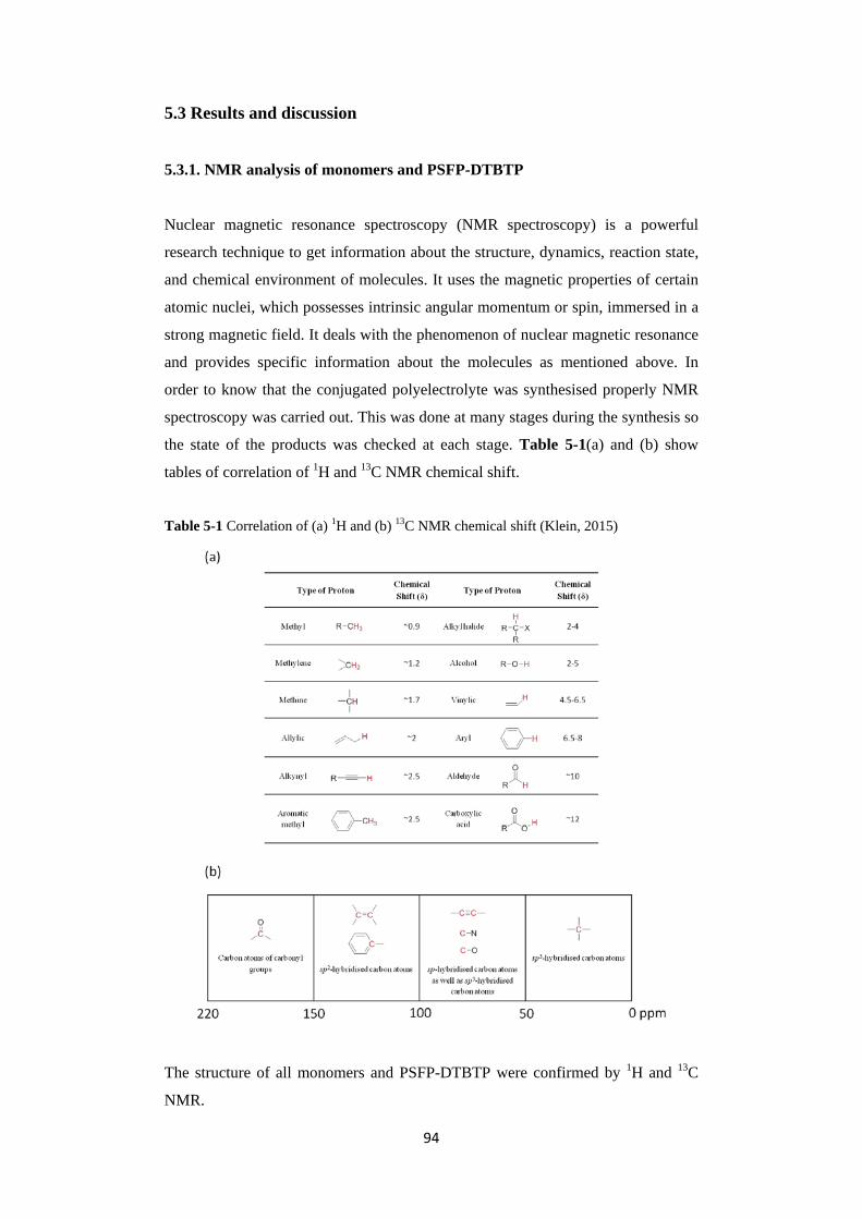
5.3 Results and discussion
5.3.1. NMR analysis of monomers and PSFP-DTBTP
Nuclear magnetic resonance spectroscopy (NMR spectroscopy) is a powerful
research technique to get information about the structure, dynamics, reaction state,
and chemical environment of molecules. It uses the magnetic properties of certain
atomic nuclei, which possesses intrinsic angular momentum or spin, immersed in a
strong magnetic field. It deals with the phenomenon of nuclear magnetic resonance
and provides specific information about the molecules as mentioned above. In
order to know that the conjugated polyelectrolyte was synthesised properly NMR
spectroscopy was carried out. This was done at many stages during the synthesis so
the state of the products was checked at each stage. Table 5-1(a) and (b) show
tables of correlation of 1H and 13C NMR chemical shift.
Table 5-1 Correlation of (a) 1H and (b) 13C NMR chemical shift (Klein, 2015)
The structure of all monomers and PSFP-DTBTP were confirmed by 1H and 13C
NMR.
94

Figure 5-1 (a) 1H NMR and (b) 13C NMR spectra of 2,7-dibromo-9,9-bis(4-sulfonatobutyl)
fluorene disodium.
All NMR data from the monomers and PSFP-DTBTP are shown in Figures 5-1 to
5-5. Figure 5-1(a) and (b) shows the 1H and 13C NMR of synthesis of 2,7-
Dibromo-9,9-bis(4-sulfonatobutyl)fluorene disodium (1). In 1H NMR, proton peaks
of aromatic compounds are shown between 7.7 and 7.4 ppm and proton peaks of
alkyl chains appear from 2.6 to 0.4 ppm (the deuterium oxide (solvent) peak
appears at 4.8 ppm). In 13C NMR, carbon peaks of aromatic rings are indicated
between 168 and 120 ppm and alkyl chains’ peaks are shown from 55 to 22 ppm.
95

All the peaks are well matched with expected peaks chemical shift, confirming a
successful synthesis.
Figure 5-2 (a) 1H NMR and (b) 13C NMR spectra of 2,7-dibromo-2,1,3-benzothiadiazole.
Figure 5-2(a) and (b) shows the 1H and 13C NMR spectra of 4,7-dibromo-2,1,3-
benzothiadiazole (2). For this molecule (2), only one proton is in the aromatic
group, so only one proton peak shows at 7.75 ppm (other peaks are chloroform-d
(solvent) peak at 7.24 ppm and water peak at 1.5 ppm). In the 13C NMR spectrum,
three carbon peaks from the aromatic group appear at 152.99, 132.38, and 113.94
96

ppm (the chloroform-d (solvent) peak is shown at 77.23 ppm). The solvent peak is
always shown in the NMR spectrum and this peak appears at a specific point
(77.23 ppm). Therefore, the solvent peak will be shown in further NMR data.
Figure 5-3 (a) 1H NMR and (b) 13C NMR spectra of 4,7-di-2-thienyl-2,1,3-
benzothiadiazole
Figure 5-3(a) and (b) is the 1H and 13C NMR spectra of 4,7-di-2-thienyl-2,1,3-
benzothiadiazole (3). The proton peaks of the material appeared at 8.11, 7.88, 7.45,
97

and 7.21 ppm corresponding to aromatic rings in 1H NMR. Three more peaks are
shown in comparison with (2) in the spectrum. The seven carbon peaks are shown
between 152.5 and 125.8 ppm in 13C NMR and four more peaks appeared in the
spectrum. From the two NMR data, it is evident that the molecule is well
synthesised.
Figure 5-4 1H NMR spectrum of 4,7-bis(5-bromo-2-thienyl)-2,1,3-benzothiadizole.
Figure 5-4 shows the 1H NMR spectrum of 4,7-bis(5-bromo-2-thienyl)-2,1,3-
benzothiadizole (4). Three proton peaks in the aromatic group emerged at 7.80,
7.78, and 7.15 ppm. One proton peak was removed due to bromine attached to the
ring in this material and the peaks are slightly shifted by a change of electron
density due to the bromine within the molecule. Small impurity peaks also
appeared as well as a big water peak. This indicated the sample was not well
purified and dried.
98

Figure 5-5 1H NMR spectrum of conjugated polyelectrolyte PSFP-DTBTP.
The 1H NMR spectrum of PSFP-DTBTP is shown in Figure 5-5. In 1H NMR,
proton peaks of aromatic compounds are broadly present between 8.39 and 6.78
ppm and proton peaks of alkyl chains appear from 3.88 to 0.6 ppm.
All the synthesised materials are analysed by 1H and 13C NMR spectra. In the
analysis, the molecular weight of PSFP-DTBTP was not measured by gel
permeation chromatography (GPC) due to this technique generating inaccurate data
for water soluble polymers. In general, for water-soluble polymers it is hard to
measure molecular weight (Mw) because it is not well dissolved in the organic
solvent required for GPC and even if it is dissolved in protic solvent such as
DMSO, the molecular weight of the polymer is not accurate. Therefore, the Mw of
PSFP-DTBTP was predicted by dialysis membrane molecular weight cut-off
(MWCO). The molecular weight of dialysis membrane in this experiment was
12,400, so the Mw of polyelectrolyte should be over 12,400.
In addition, PSFP-DTBTP was synthesised three times in three different batches.
However, the polyelectrolyte from a single batch was used for all experiments in
the research to ensure consistency.
5.3.2. FT-IR spectrum of PSFP-DTBTP
Infrared (IR) spectroscopy measures the transmittance within the infrared region of
the electromagnetic spectrum. This technique is used to identify and study
chemicals by identifying what functional groups they have. To understand the
99

components of the polymer backbone and its functional groups, PSFP-DTBTP
solid was measured by FT-IR spectroscopy. Table 5-2 shows the IR spectroscopy
correlation table of some functional groups.
Table 5-2 Correlation IR absorption signals of some functional groups (McMurry, 1996)
Functional group class Band position (cm-1) Intensity of absorption
Alkanes, alkyl groups
C H
2850-2960
Medium to strong
Alkenes
C H C C
3020-3100
1640-1680
Medium
Medium
Alkynes
C H C C
3300
2100-2260
Strong
Medium
Alkyl halides
C Cl C Br C I
600-800
500-600
500
Strong
Strong
Strong
Alcohols
O H C O
3400-3650
1050-1150
Strong and broad
Strong
Aromatics
C H
CCC
CC C
3030
1600, 1500
Medium
Strong
Amines N H C N
3300-3500
1030, 1230
Medium
Medium
Carbonyl compounds
C O
1680-1750
Strong
Carboxylic acids
O H
2500-3100
Strong and very broad
Nitriles
C N
2210-2260
Medium
Nitro compounds
NO2
1540
Strong
100

The FT-IR spectrum of PSFP-DTBTP is illustrated in Figure 5-6. Vibration bands
of sulfonate groups in PSFP-DTBTP are confirmed at 1042 and 1167 cm-1 and this
is well matched with previous reports at approximately 1040 and 1180 cm-1
(Borozenko et al., 2014, Martins et al., 2003). The bands of aromatic rings in
PSFP-DTBTP were evident at 1462 and 1600 cm-1. Aromatic C-C stretch peaks
appeared at 1462 and 1602 cm-1. C-H stretch peak of alkyl chain in polyelectrolyte
also appeared at 2870 cm-1. All the peaks are well matched with previous reports
and the correlating IR functional peaks. Therefore, we can confirm the all
functional groups expected are present in the PSFP-DTBTP.
4000 3500 3000 2500 2000 1500 1000404550556065707580859095
100
Tran
smitt
ance
(%)
Wavenumber (cm-1)
C-H
C-C (aromatic ring)
S-O
Figure 5-6 ATR FT-IR spectrum of PSFP-DTBTP.
5.3.3. Optical properties of PSFP-DTBTP
To characterise the optical properties, a thin film of the conjugated polyelectrolyte
was prepared on a clean glass substrate. 5 mg of the conjugated polyelectrolyte was
dissolved in 1 ml of deionised water. The solution was spin-cast on the glass
substrate at 6000 rpm for 40 sec and thermally annealed at 150 °C for 15 min.
Figure 5-7(a) shows UV-vis absorption spectra and PL spectrum of PSFP-DTBTP
solution in water and a thin film of PSFP-DTBTP. Corresponding photos of the
solution and the films are shown in the Figure 5-7(b).
101

Figure 5-7 (a) UV-vis absorption spectra of PSFP-DTBTP solution in water (2.76 X 10⁻⁵ M
[R. U.]) (black) and PSFP-DTBTP film (red) and PL spectrum of PSFP-DTBRP film (blue),
(b) photographs of PSFP-DTBTP solution (1) and film (2) and film (3) taken under uv
illumination.
The PSFP-DTBTP film shows a strong absorption peak at 366 nm from the
fluorene-phenylene groups and a very weak absorption peak at around 530 nm with
a shoulder edge around 590 nm from di-thienyl benzothiadiazole-phenylene groups.
This result was red-shifted by about 8 nm from the PSFP-DTBTP solution peak at
358 nm due to a conjugation length change of rigid conjugated polymer backbone
in the thin film. The number of aromatic rings along the backbone of the polymer
determines its conjugation length. In the solution, the aromatic rings easily rotate
relative to each other through the single bond in the polymer backbone. In the solid
state, however, fewer twists of the polymer backbone increases co-planarity.
Therefore, conjugation length of the polymer is increased in the solid state and the
absorbance of the polymer film is slightly red-shifted. It was not possible to
confirm that the peak of DTBTP group around 530 nm was changed from solution
because of the weak signal strength, however the absorption peak strength of the
film around 530 nm was increased compared to the solution peak. The PL spectrum
of PSFP-DTBTP film showed a strong fluorescence peak at 647 nm, even though
they had a strong absorption peak at 366 nm. The emission peak of molecules
normally shows an absorbance edge peak due to the energy band gap of the system.
102

Excited electrons which are generated by absorption of light in molecules move to
the conduction band edge and they emit fluorescence when they relax down from
lowest conduction band (LUMO) to the valence band (HOMO). In such cases, the
band gap energy is matched with the absorption band edge of the molecules.
However, PSFP-DTBTP shows red fluorescence. This is because of exciton
migration effects, they migrate from the electron donating fluorene group to the
electron accepting benzothiadiazole group in the polyelectrolyte (Bardeen, 2011,
Lee et al., 2011). These results were as expected because similar UV-vis absorption
and PL peaks have been observed in previous reports.
5.3.4. Cyclic voltammetry (CV) measurement of PSFP-DTBTP
The intention was to use PSFP-DTBTP as both an active layer and interfacial layer
in photovoltaic cells, therefore CV was carried out to measure its electronic energy
levels. A CV measurement is used to study the oxidation and reduction properties
of the material and it is a useful technique to understand the HOMO and LUMO
level of materials. The CV measurement of PSFP-DTBTP was performed in the
presence of tetrabutylammonium perchlorate (0.1 M) as an electrolyte in
acetonitrile and Ag/Ag+ reference electrode (Ag wire in 0.01 M AgNO3 solution).
For calibration, the energy level of HOMO and LUMO was calculated using the
equations below (Liang et al., 2009).
EHOMO = −(∅ox + 4.8 − 0.082) eV
ELUMO = −(∅red + 4.8 − 0.082)eV
Where ∅ox and ∅red are the onset oxidation point and onset reduction point vs.
Ag/Ag+ respectively. This equation is based on the redox potential of
ferrocene/ferrocenium being -4.8 eV in absolute energy level below the vacuum
level (located at 0.082 V to the Ag/Ag+ electrode).
A CV curve of PSFP-DTBTP is shown in Figure 5-8. The onset point of oxidation
∅ox is determined to be 0.66 V, which is determined by intersection point of two
tangents (red lines in the Figure 5-8), and the energy level of highest occupied
molecular orbital (HOMO) was calculated at -5.38 eV using the equation above.
The reduction onset point is -1.33 V and the energy level of lowest unoccupied
molecular orbital (LUMO) was calculated at -3.39 eV. Therefore, PSFP-DTBTP
has band gap of 1.99 eV and it is well matched with UV-vis absorption spectrum,
103

although it was very weak peak at around 530 nm in PSFP-DTBTP, the spectral
edge of PSFP-DTBTP absorption is around 600 nm. To convert wavelength to
energy, it is calculated by Plank-Eistein relation below;
E = hν
ν =cλ
E =hcλ
From the equation, where E is the energy of photon, ν is frequency, h is the Plank
constant, and c is speed of light.
Figure 5-8 Cyclic Voltammetry (CV) diagram of PSFP-DTBTP.
These results were compared to a similar CPE material poly[(9,9-bis(3'-(N,N-
dimethylamino)propyl)-2,7-fluorene)-alt-2,7-(9,9–dioctylfluorene)] (PFN, fluorene
groups are included). The energy levels compared reasonably well with PFN
(HOMO of -5.61 eV and LUMO of -2.14 eV) (Zhang et al., 2010). The effect of
the fluorene side group and the donor and acceptor nature of PSFP-DTBTP
resulted in a lower oxidation and reduction potential than PFN. The ionic sulfonyl
groups of PSFP-DTBTP lead to easier oxidation than the general fluorine. The
DTBTP groups gave the polymer a lower reduction potential and lower band gap
than PFN due to the donor and acceptor structure of the polymer (Cheng et al.,
2009). Hou et al. reported fluorene-based red-emitting copolymer (9,9-
dioctylfluorene and 4,7-di-2-thienyl-2,1,3-benzothiadiazole, PFO-DBT) (Hou et al.,
2002). In the report, the HOMO and LUMO levels were slightly altered by
104

different ratios of fluorene and benzothiadiazole parts but generally the HOMO
was -5.47 to -5.61 eV and the LUMO was -3.46 to -3.54 eV. As mentioned above,
PSFP-DTBTP showed a slightly higher HOMO and LUMO level than PFO-DBT.
However, PSFP-DTBTP showed higher band gap than PCDTBT (HOMO of -5.4
eV and LUMO of -3.6 eV). This is attributed to PSFP-DTBTP (blocked copolymer)
consisting of 90% of fluorene groups (donor) and 10% of dithienyl-
benzothiadiazole groups (acceptor). There is a relatively small amount og the
acceptor groups compared to the donor groups. However, in comparison PCDTBT
has alternating 1:1 donor and acceptor groups, so in PCDTBT the electrons are
more readily moved from donors to acceptors.
5.4. Conclusions
The low band gap conjugated polyelectrolyte PSFP-DTBTP was synthesised and
its structure was confirmed by NMR and IR. It dissolves easily at a concentration
of <30 mg/ml in water. The CPE had sulfonate side chains in the fluorene groups
to aid dissolution in water and this CPE had donor and acceptor groups in the
polymer backbone. PSFP-DTBTP showed a strong absorption peak at 366 nm and
a weak absorption peak at 530 nm. It showed red fluorescence and the PL peak was
at 647 nm due to intramolecular charge transfer from the fluorene groups (donor)
to the benzothiadiazole groups (acceptor) within the polymer backbone. The
HOMO and LUMO energy levels were determined by CV to be -5.38 and-3.39 eV
and the band gap of the CPE was found to be 1.99 eV. This CPE was synthesised
in order to address the challenge of applying CPEs in PVCs and the electronic
energy levels measured were suitable for application in PVCs.
5.5. References
BARDEEN, C. 2011. Exciton Quenching and Migration in Single Conjugated
Polymers. Science, 331, 544-545.
BOROZENKO, O., MACHADO, V., SKENE, W. G. & GIASSON, S. 2014.
Organophosphonic acids as viable linkers for the covalent attachment of
polyelectrolyte brushes on silica and mica surfaces. Polymer Chemistry, 5,
5740-5750.
105

CHENG, Y. J., YANG, S. H. & HSU, C. S. 2009. Synthesis of Conjugated
Polymers for Organic Solar Cell Applications. Chemical Reviews, 109,
5868-5923.
DUAN, C. H., CAI, W. Z., HSU, B. B. Y., ZHONG, C. M., ZHANG, K., LIU, C.
C., HU, Z. C., HUANG, F., BAZAN, G. C., HEEGER, A. J. & CAO, Y.
2013. Toward green solvent processable photovoltaic materials for
polymer solar cells: the role of highly polar pendant groups in charge
carrier transport and photovoltaic behavior. Energy & Environmental
Science, 6, 3022-3034.
GRIMSDALE, A. C., CHAN, K. L., MARTIN, R. E., JOKISZ, P. G. & HOLMES,
A. B. 2009. Synthesis of Light-Emitting Conjugated Polymers for
Applications in Electroluminescent Devices. Chemical Reviews, 109, 897-
1091.
HOU, J. H., CHEN, H. Y., ZHANG, S. Q. & YANG, Y. 2009. Synthesis and
Photovoltaic Properties of Two Benzo[1,2-b:3,4-b ']dithiophene-Based
Conjugated Polymers. Journal of Physical Chemistry C, 113, 21202-21207.
HOU, Q., XU, Y. S., YANG, W., YUAN, M., PENG, J. B. & CAO, Y. 2002.
Novel red-emitting fluorene-based copolymers. Journal of Materials
Chemistry, 12, 2887-2892.
KWAK, C. K., KIM, D. G., KIM, T. H., LEE, C. S., LEE, M. & LEE, T. S. 2010.
Simultaneous and Dual Emissive Imaging by Micro-Contact Printing on
the Surface of Electrostatically Assembled Water-Soluble Poly(p-
phenylene) Using FRET. Advanced Functional Materials, 20, 3847-3855.
KWON, N. Y., KIM, D., SON, J. H., JANG, G. S., LEE, J. H. & LEE, T. S. 2011.
Simultaneous Detection and Removal of Mercury Ions in Aqueous
Solution with Fluorescent Conjugated Polymer-Based Sensor Ensemble.
Macromolecular Rapid Communications, 32, 1061-1065.
LEE, J. H., KIM, D. G., KWON, N. Y., JANG, G. S., SON, J. H., LEE, M., CHO,
H. J., KWEON, H. S. & LEE, T. S. 2011. Protein-Induced Aggregation of
Fluorescent Conjugated Polyelectrolytes with Sulfonate Groups: Synthesis
and Its Sensing Application. Journal of Polymer Science Part a-Polymer
Chemistry, 49, 138-146.
LIANG, Y. Y., FENG, D. Q., WU, Y., TSAI, S. T., LI, G., RAY, C. & YU, L. P.
2009. Highly Efficient Solar Cell Polymers Developed via Fine-Tuning of
Structural and Electronic Properties. Journal of the American Chemical
Society, 131, 7792-7799.
106

LIU, B. & BAZAN, G. C. 2004. Interpolyelectrolyte complexes of conjugated
copolymers and DNA: Platforms for multicolor biosensors. Journal of the
American Chemical Society, 126, 1942-1943.
LIU, M. F., CHEN, Y. L., ZHANG, C., LI, C. H., LI, W. W. & BO, Z. S. 2013.
Synthesis of thiophene-containing conjugated polymers from 2,5-
thiophenebis(boronic ester)s by Suzuki polycondensation. Polymer
Chemistry, 4, 895-899.
MARTINS, C. R., RUGGERI, G. & DE PAOLI, M. A. 2003. Synthesis in pilot
plant scale and physical properties of sulfonated polystyrene. Journal of
the Brazilian Chemical Society, 14, 797-802.
MCMURRY, J. 1996. Organic chemistry, Pacific Grove, CA ; London,
Brooks/Cole.
PU, K. Y., LI, K. & LIU, B. 2010. Multicolor Conjugate Polyelectrolyte/Peptide
Complexes as Self-Assembled Nanoparticles for Receptor-Targeted
Cellular Imaging. Chemistry of Materials, 22, 6736-6741.
PU, K. Y. & LIU, B. 2010. Fluorescence Turn-on Responses of Anionic and
Cationic Conjugated Polymers toward Proteins: Effect of Electrostatic and
Hydrophobic Interactions. Journal of Physical Chemistry B, 114, 3077-
3084.
QIAO, Q. Q., SU, L. Y., BECK, J. & MCLESKEY, J. T. 2005. Characteristics of
water-soluble polythiophene: TiO2 composite and its application in
photovoltaics. Journal of Applied Physics, 98.
SEO, J. H., GUTACKER, A., SUN, Y. M., WU, H. B., HUANG, F., CAO, Y.,
SCHERF, U., HEEGER, A. J. & BAZAN, G. C. 2011. Improved High-
Efficiency Organic Solar Cells via Incorporation of a Conjugated
Polyelectrolyte Interlayer. Journal of the American Chemical Society, 133,
8416-8419.
SON, J. H., JANG, G. & LEE, T. S. 2013. Synthesis of water-soluble, fluorescent,
conjugated polybenzodiazaborole for detection of cyanide anion in water.
Polymer, 54, 3542-3547.
YANG, J. H., GARCIA, A. & NGUYEN, T. Q. 2007. Organic solar cells from
water-soluble poly(thiophene)/fullerene heterojunction. Applied Physics
Letters, 90.
YANG, N. J., LIAO, C. S. & CHEN, S. A. 2010. Hysteresis in Conjugated
Polymer Thin Film Transistors Generated by Chain Relaxation. Advanced
Functional Materials, 20, 1000-1004.
107

YANG, R. Q., TIAN, R. Y., YAN, J. G., ZHANG, Y., YANG, J., HOU, Q.,
YANG, W., ZHANG, C. & CAO, Y. 2005. Deep-red electroluminescent
polymers: Synthesis and characterization of new low-band-gap conjugated
copolymers for light-emitting diodes and photovoltaic devices.
Macromolecules, 38, 244-253.
YAO, K., CHEN, L., CHEN, Y. W., LI, F. & WANG, P. S. 2011. Influence of
water-soluble polythiophene as an interfacial layer on the P3HT/PCBM
bulk heterojunction organic photovoltaics. Journal of Materials Chemistry,
21, 13780-13784.
YU, D. Y., ZHANG, Y. & LIU, B. 2008. Interpolyelectrolyte complexes of anionic
water-soluble conjugated polymers and proteins as platforms for multicolor
protein sensing and quantification. Macromolecules, 41, 4003-4011.
ZHANG, L. J., HE, C., CHEN, J. W., YUAN, P., HUANG, L. A., ZHANG, C.,
CAI, W. Z., LIU, Z. T. & CAO, Y. 2010. Bulk-Heterojunction Solar Cells
with Benzotriazole-Based Copolymers as Electron Donors: Largely
Improved Photovoltaic Parameters by Using PFN/A1 Bilayer Cathode.
Macromolecules, 43, 9771-9778.
ZHOU, H. Q., ZHANG, Y., MAI, C. K., COLLINS, S. D., NGUYEN, T. Q.,
BAZAN, G. C. & HEEGER, A. J. 2014. Conductive Conjugated
Polyelectrolyte as Hole-Transporting Layer for Organic Bulk
Heterojunction Solar Cells. Advanced Materials, 26, 780-785.
108

6. Polymer photovoltaic cells with conjugated
polyelectrolyte
6.1. Introduction
Conjugated polyelectrolytes (CPEs) are conjugated polymers that contain ionic
charged side chains which give it water-solubility (Huang et al., 2005, Tran-Van et
al., 2004, Huang et al., 2004, Stork et al., 2002, Gaylord et al., 2001). During the
past decade, CPEs have been used within the active layer (Yang et al., 2007,
McLeskey and Qiao, 2006), electron transporting layers (ETLs) or hole
transporting layers (HTLs) in OPVCs. CPEs when used as interlayers helped to
improve the PCE of devices (Zhou et al., 2014, Duan et al., 2013, Seo et al., 2011,
Zhang et al., 2010, He et al., 2011).
Yang et al. and McLeskey and Qioao reported water-soluble polythiophene based
photovoltaic cells. Poly[2-(3-thienyl)-ethoxy-4-butylsulfonate] (PTEBS) was used
as a water-soluble polythiophene. Yang et al. applied PTEBS and C60 as the
electron donor and hole transporting layer and 2,9-dimethyl-4,7-diphenyl-1,10-
phenanthroline (BCP) was used as the exciton blocking layer. They achieved a
PCE of 0.43%. McLeskey and Qioao reported organic solar cells made from
PTEBS and TiO2. PTEBS was used as the electron donor and TiO2 as the electron
acceptor. The highest PCE of the devices produced was 0.13%.
Seo et al. and Zhou et al. reported fluorene and cyclopenta-dithiophene based CPE
as materials for application in thin ETLs and HTLs, respectively and showed an
improvement of JSC, VOC, FF and PCE. Seo et al. reported that PCDTBT based
PVCs achieved a PCE of over 6% with a positively charged poly[3-(6-
trimethylammoniumhexyl)thiophene] (P3TMAHT) or poly(9,9-bis(2-ethylhexyl)-
fluorene]-b-poly[3-(6-trimethylammoniumhexyl)thiophene] (PF2/6-b-P3TMAHT)
interlayer where the employed device architecture was
ITO/PEDOT:PSS/PCDTBT:PC71BM/CPE/Al (Seo et al., 2011). Zhou et al.
showed an improvement of JSC, VOC, FF and PCE using CPE-K negatively charged
conjugated polyelectrolyte as a HTL instead of PEDOT:PSS. The solar cell
performance was increased up to 8.2% and their device structure was ITO/CPE-
K/PTB7:PC71BM/Ca/Al (Zhou et al., 2014).
109

The use of a PSFP-DTBTP as both as an active layer and hole transporting layer is
described in this chapter. Conjugated polyelectrolyte was synthesised as described
in Chapter 5 for use both as an active layer material therefore avoiding the need
for organic solvents and also as an additive in the hole transporting layer so as to
improve the efficiency of OPVCs. Improving the device efficiency is expected to
improve the overall sustainability of OPVC fabrication by reducing the quantites of
materials needed per Watt of power produced. Unfortunately, PSFP-DTBTP did
not show any photovoltaic behaviour as an active layer material, but it did show an
increase of the PCE and reproducibility of OPVC performance as an additive in the
PEDOT:PSS layer.
6.2. Experimental
6.2.1. Materials
Poly(3,4-ethylenedioxythiophene) with poly(styrenesulfonate) (PEDOT:PSS – HC
Stark Clevios P VP AI4083 (M121)), poly[N-9”-hepta-decanyl-2,7-carbazole-alt-
5,5-(4’,7’-di-2-thienyl-2’,1’,3’-benzothiadiazole)] (PCDTBT, (M1311) Mw:
34,900), [6,6]-phenyl-C71-butyric acid methyl ester (PC71BM), Poly(3-
hexylthiophene-2,5-diyl) (P3HT, (M106) RR: 94.7%, Mw: 34,100), [6,6]-phenyl-
C61-butyric acid methyl ester (PCBM), Indium tin oxide (ITO) glass substrates
(S171, 20 Ω/square), and UV-epoxy resin were purchased from Ossila Ltd. Water-
soluble C60 (C60-(N,N-dimethyl pyrrolidinium iodide)) was purchased from
Solaris Chem Inc..
6.2.2. Organic photovoltaic cell fabrication (PSFP-DTBTP used as active layer)
PSFP-DTBTP was synthesised as explained in Chapter 5 for use as an active layer.
Pre-patterned ITO glass substrates were washed with Hellmanex solution, iso-
propyl alcohol (IPA), and deionised (DI) water in an ultrasonic bath for 10 min
each. The substrates were then dump rinsed twice in hot deionised water and once
in cold deionised water. For the ITO/PEDOT:PSS/PSFP-DTBTP:W-C60/Ca/Al
structured devices, PEDOT:PSS (filtered by 0.45 µm PVDF filter) was spin coated
on the ITO glass substrate and thermally annealed for 15 min at 150 °C. A blend of
PSFP-DTBTP and W-C60 (1:4 volume ratio) was spin coated at 2000 rpm on the
PEDOT:PSS and thermally annealed at 150 °C for 15 min. For the
110

ITO/PEDOT:PSS:PSFP-DTBTP:W-C60/Ca/Al structured devices, PEDOT:PSS
and PSFP-DTBTP:W-C60 were mixed in a 1:1 volume ratio. The mixture of
PEDOT:PSS and PSFP-DTBTP:W-C60 was then spin coated at 2000 rpm and
thermally annealed at 150 °C for 15 min. For ITO/PEDOT:PSS/PSFP-
DTBTP/PCBM/Ca/Al, PEDOT:PSS was spin coated at 5000 rpm and annealed at
150 °C for 15 min on the ITO glass substrate and then PSFP-DTBTP was spin
coated at 2000 rpm on the PEDOT:PSS layer and annealed at 150 °C. The substrate
was then moved into the glovebox and PCBM (25 mg/ml) was spin coated at 2000
rpm on the PSFP-DTBTP layer. All the cathode layers for these various devices
structures were deposited onto the active layer in a vacuum evaporator. Calcium
(2.5 nm) and aluminium (100 nm) cathodes were deposited under 1 x 10⁻⁶ mbar.
Devices were subsequently thermally annealed on a hot plate at 80 °C 15 min. All
devices were finally encapsulated using uv-epoxy resin and a glass cover slide.
6.2.3. Organic photovoltaic cells fabrication (PSFP-DTBTP used as HTL or
additive in HTL)
All materials for device fabrication were purchased from Ossila Ltd. and used
without further treatment apart from CPE and metals for electrodes. The device
architecture used was glass substrate/ITO/hole transporting layer
(HTL)/polymer:PC71BM/calcium (Ca)/aluminium (Al). PCDTBT:PC71BM (1:4 by
weight, 20 mg/ml) or P3HT:PCBM (1:0.8 by weight, 25 mg/ml) were used as
active layer materials. Pre-patterned ITO glass substrates were cleaned with the
same process above mentioned. The HTL solution was filtered by PVDF filter
(0.45 µm) and was spin-coated on the ITO substrate at 6000 rpm then annealed at
150 °C on a hot plate for 15 min. For the PCDTBT solar cells, PCDTBT (4 mg)
was dissolved in chlorobenzene and the solution was heated at 80 °C with stirring
overnight to fully solubilise. This was then mixed with PC71BM (16 mg) and the
blend solution was heated at 80 °C for 2 h. The blend solution was filtered with
PTFE (0.45 µm) before use. The blended mixture of PCDTBT:PC71BM was spin
coated on the HTL at 700 rpm to achieve a thickness of ~75 nm as measured by J.
A. Woollam Co. M-2000 ellipsometer. For the P3HT solar cells, solutions (25
mg/ml in chlorobenzene) of P3HT and PCBM were prepared separately in
chlorobenzene and heated at 70 °C overnight. The P3HT and PCBM solutions were
then mixed by volume portion of 1:0.8. A blend of P3HT and PCBM solution was
heated at 70 °C over 3 h to fully dissolve and then filtered before use. The blended
mixture of P3HT:PCBM was spin coated on the HTL at 2000 rpm to give a
111

thickness of ~70 nm. Calcium (2.5 nm) and aluminium (100 nm) cathodes (for
PCDTBT solar cell) or aluminium (100 nm) cathode (for P3HT solar cells) were
deposited onto the active layer in a vacuum evaporator. The base pressure of
evaporation chamber was less than 1 x 10⁻⁶ mbar. Devices were thermally
annealed on a hot plate at 80 °C (for PCDTBT PVCs) for 15 min or 150 °C (for
P3HT PVCs) for 30 min. All devices were finally encapsulated by UV-epoxy resin
and a glass cover slide.
6.2.4. Preparation of films for characterisation
In order to measure UV-vis absorption, thickness, AFM, and PL of the HTL,
PEDOT:PSS or PEDOT:PSS:PSFP-DTBTP thin films similar samples were spin-
coated at 6000 rpm for 40 sec on to glass substrates, silicon wafer or ITO patterned
glass substrates. The glass substrates were cleaned using the same procedure used
to prepare ITO substrates and the thin films were thermally annealed on a hotplate
at 150 °C for 15 min after spinning. For the PL measurement of PSFP-DTBTP and
PCDTBT, PSFP-DTBTP solution of 15 mg/ml in water were spin-coated at 6000
rpm for 40 sec on glass substrates and thermally annealed at 150 °C for 15 min
then, PCDTBT (4 mg/ml in chlorobenzene) was spin-coated at 700 rpm for 30 sec
and thermally annealed at 80 °C for 15 min.
6.2.5. Instruments
NMR, EA, UV-vis, PL, FT-IR, and CV for analysis of polymer are described in
synthesis Chapter 5. The Ultraviolet photoemission spectroscopy (UPS) data was
collected using the Kratos Axis Ultra DLD instrument with a helium (He) source.
A 5 eV pass energy was set, and an area of 110 µm diameter analysed. The data
was collected between 25 eV to 0 eV in steps of 0.025 eV and for a 200 ms dwell
time. The thickness of the HTL thin films were measured using a J. A. Woollam
Co. M-2000 ellipsometer with a charge-coupled devices (CCD) camera detector.
Atomic force microscope (AFM) images were obtained using a Veeco Dimension
3100 AFM with a Nanoscope IIIa controller and basic extender. It was operated in
tapping mode with Bruker TESPA tapping mode cantilevers with a nominal spring
constant of 42 N/m and a nominal resonant frequency of 320 kHz.
Photoluminescence spectra were collected by Keithley 2700 multimeter with
Laser- LDCU CW 450nm diode laser and detector was silicon diode. Samples were
measured under vacuum at approximately 1 x 10⁻³ mbar.
112

6.3. Use PSFP-DTBTP in active layer
In order to reduce the usage of organic solvents for devices, a CPE was synthesised
and applied as part of the active layer. As mentioned in the synthesis Chapter 5,
the CPE has donor and acceptor parts and it showed low band gap about 2.0 eV.
6.3.1. Thickness change of PEDOT:PSS HTL caused by spin casting
subsequent water soluble layers
Before using PSFP-DTBTP as an active layer, it was necessary to test the thickness
of the PEDOT:PSS after spin casting water on top of the HTL to check whether the
PEDOT:PSS is entirely washed away during the process or not. Water was spin
cast on top of both an annealed and as cast PEDOT:PSS films. Because both
materials can be dissolved in water the PEDOT:PSS may be washed away by spin
coating subsequent water based solutions. Thin films of PEDOT:PSS were
fabricated on the pieces of silicon wafer and the film thickness was measured by
ellipsometry. To measure thickness before and after water casting on the
PEDOT:PSS film, PEDOT:PSS was spin coated at 5000 rpm on the silicon wafer
then one sample was not annealed and another sample was annealed at 150 °C for
15 min. Two of each type of film was made. Water was spin coated on each
PEDOT:PSS film at 2000 rpm. The thickness of all four films was measured.
Table 6-1 shows the change of thickness before and after water casting with non-
annealed and annealed at 150 °C PEDOT:PSS.
Table 6-1 The average film thickness of non-annealed and annealed PEDOT:PSS before
and after water casting (the data was collected by 2 films of each condition)
Samples Thickness of film
Before water drop
Thickness of film
After water drop
Non-annealed 45 ± 1 nm 3 ± 1.5 nm
Annealed at 150 °C 42 ± 0.6 nm 31 ± 1 nm
As shown in Table 6-1, almost all PEDOT:PSS was washed out by water at non-
annealed film, but the PEDOT:PSS film annealed at 150 °C showed 42 and 31 nm
thickness before and after water dropping respectively.
113

6.3.2. Fabrication of water-based photovoltaic cells
To fabricate a water based BHJ photovoltaic cell, both PCBM and water-soluble
C60 (W-C60) (C60-(N,N-dimethyl pyrrolidinium iodide)) was used as an electron
acceptor. The molecular structures of materials are shown in Figure 6-1.
Figure 6-1 Structures of water-soluble C60 and PCBM.
Four types of device structure were produced as shown in Figure 6-2. The
architecture shown in Figure 6-2(a) is similar to the usual BHJ OPVC with an
active layer consisting of a blend of CPE and W-C60 and the concentration of CPE
and W-C60 was 25 mg/ml (1:4 volume blend ratio). The blend of CPE:W-C60 and
PEDOT:PSS used in Figure 6-2(b) was prepared in a 1:1 volume ratio. This device
architecture required only one spin-casting step for all the organic materials. In
Figure 6-2(c) the blend of CPE and PEDOT:PSS was 1:1 by volume ratio and
PCBM (25 mg/ml) was used as an electron transporting layer. In order to avoid
aggregation of CPE and W-C60, PCBM was applied in the device as a separate
layer. In Figure 6-2(d), the concentrations of CPE and PCBM were 25 mg/ml. This
architecture of device has a bi-layer structure rather than a BHJ active layer in the
device to compare to device’s architectures in Figure 6-2(a) and (c).
Figure 6-2 Four kinds of architecture of devices using PSFP-DTBTP as an active layer.
114

Unfortunately, none of these devices showed any photovoltaic behaviour. There
were two possible reasons for this. First, when making the blend of CPE and W-
C60, many aggregations of solids appeared. It may be that because CPE and W-
C60 are negatively and positively charged materials respectively they are bind well
together to form aggregates and therefore fall out of solution prior to spin casting.
Even if CPE and W-C60 were dissolved in solvent separately, they still made
precipitates after mixing them. As a result, the solution was much too transparent
after filtering. Filtering is needed to fabricate uniform films free of defects by
removing undissolved or large particles. Therefore, it was not possible to make a
proper functioning bulk-heterojunction layer from the materials due to their
aggregation. Secondly, the absorption wavelength of the CPE is short. As shown in
Figure 5-9 in Chapter 5, the main absorption peak of PSFP-DTBTP is around 370
nm and only a weak absorption peak is shown around 530 nm. Therefore, although
CPE absorbs the short wavelengths, a lot of photons pass thorough the active layer
at longer wavelength so the devices cannot harvest large amounts of photons. In
order to increase of absorption around 530 nm, CPE was synthesised using 1:1
ratio of donor (fluorene group) and acceptor (dithienyl-benzothiadiazole group).
However, when the relative fraction of acceptor groups was increased, the polymer
would not dissolve in water.
6.4. Use PSFP-DTBTP in HTL
In order to study the PCE of devices made using CPE as an additive in the HTL or
as a replacement HTL, photovoltaic cells with typical blends of PCDTBT and
PC71BM and P3HT with PCBM as the active layer BHJ were fabricated. ITO and
calcium/aluminium (Ca/Al) were used as the anode and cathode materials,
respectively. Device architecture of the OPVCs was ITO/PEDOT:PSS:PSFP-
DTBTP /Active layer/(Ca)/Al and they were compared to more standard
ITO/PEDOT:PSS/Active layer/(Ca)/Al reference devices. In this Chapter, a Ca/Al
cathode layer was used for PCDTBT PVCs to allow direct comparison to the P3HT
PVCs. According to previous reports (Watters et al., 2012), PCDTBT PVCs with a
Ca/Al cathode showed high VOC, relatively high JSC and significant enhanced FF.
115

6.4.1. Optical characterisation of conjugated polyelectrolyte with PEDOT:PSS
and PCDTBT:PC71BM
Hole transporting layer blends of PEDOT:PSS:PSFP-DTBTP (with 2 mg/ml or 5
mg/ml or 8 mg/ml of the CPE dissolved in the as acquired PEDOT:PSS solution)
were named as HTL2, HTL5, and HTL8 respectively in this chapter. HTL2 related
to 2 mg of PSFP-DTBTP per 1 ml of PEDOT:PSS solution. HTL5 related to 5 mg
of PSFP-DTBTP per 1 ml of PEDOT:PSS solution. HTL8 related to 8 mg of PSFP-
DTBTP per 1 ml of PEDOT:PSS solution. Figure 6-3(a) shows the UV-vis
absorption spectra of the PSFP-DTBTP, PEDOT:PSS, HTL2, HTL5, and HTL8
thin films after spin casting onto glass substrates. To measure the UV-vis
absorption of the thin films, PSFP-DTBTP, PEDOT:PSS, HTL2, HTL5, and HTL8
were spin coated at 6000 rpm on glass substrates for 40 sec and then thermally
annealed at 150 °C for 15 min. The PSFP-DTBTP film shows a strong π-π*
absorption peak at 367 nm from fluorene-phenylene groups and a very weak
absorption peak at around 530 nm from intramolecular charge transfer between
donor and acceptor units along polymer chains. The 367 nm absorption peak
observed in the PSFP-DTBTP film was shifted by about 9 nm compared to the
solution spectra where the peak was at about 358 nm. The number of co-planar
rings along the backbone of the polymer determines its conjugation length. The
longer the conjugation length, the smaller the separation between adjacent energy
levels due to quantum confinement effects. Fewer twists in the polymer increase
the co-planarity and can result from changes in the environment. Therefore the
absorbance shift is attributed to increasing the conjugation length of the rigid
backbone in the film, when the polymer is in the sold state. However, we could not
confirm whether the peak from the DTBTP group around 530 nm was changed
from solution because of the weak signal strength. The pristine PEDOT:PSS film
did not show any specific absorption features. HTL films showed a small
absorption peak at 372 nm which increased with increasing concentration (2 mg/ml,
and 5 mg/ml) and it has a very small trace of an absorption peak at around 530 nm
from PSFP-DTBTP. The absorption peaks of HTL2 and HTL5 were slightly red
shifted from the PSFP-DTBTP peak at 367 to 372 nm. However, HTL8 was blue
shifted and had an absorption peak at 362 nm.
Although it was very weak peak at around 530 nm in PSFP-DTBTP, the spectral
edge of PSFP-DTBTP absorption is around 600 nm which equates to a band gap
116

for PSFP-DTBTP of 2.0 eV from the UV-vis absorption spectra and it was (1.99
eV) in the CV measurement in synthesis Chapter 5.
Figure 6-3 UV-vis absorption spectra of (a) PSFP-DTBTP film (black), PEDOT:PSS (red),
HTL2 (blue), HTL5 (purple), and HTL8 (green) and (b) PCDTBT (black),
PCDTBT:PC71BM (red), PEDOT:PSS/PCDTBT:PC71BM (blue), and HTL2 (purple), or
HTL5 (green), HTL8/PCDTBT:PC71BM (orange) (HTL is hole transporting layer of
PEDOT:PSS:PSFP-DTBTP).
In order to understand the combined absorption abilities of the active layer and the
HTLs, UV-vis absorption spectra of PCDTBT, PCDTBT:PC71BM (blend ratio of
1:4) and HTL/PCDTBT:PC71BM were measured and are shown in Figure 6-3(b).
All HTLs were spin coated on glass substrates at 6000 rpm and the HTLs were
thermally annealed at 150 °C for 15 min then PCDTBT:PC71BM was spin coated at
117

700 rpm on the HTL and thermally annealed at 80 °C for 15 min. The PCDTBT
film showed a strong absorption peak at 403 nm and strong broad absorption band
from 560 to 590 nm (Yi et al., 2011). The blended PCDTBT:PC71BM film showed
increased absorption ability from 300 to 580 nm due to absorption by PC71BM.
PEDOT:PSS/PCDTBT:PC71BM did not show any specific difference with
PCDTBT:PC71BM. However, HTL2, HTL5, and HTL8/PCDTBT:PC71BM films
showed a peak around 370 nm which increased with increasing CPE concentration
in the HTL and this corresponds with the results for the PSFP-DTBTP absorption
peak in Figure 6-3(a).
6.4.2. FT-IR spectra of CPE and HTL layers
4000 3500 3000 2500 2000 1500 100010
20
30
40
50
Tran
smitt
ance
(A.U
.)
Wavenumber (cm-1)
PEDOT:PSS HTL2 HTL5 HTL8
Figure 6-4 ATR FT-IR transmittance of PEDOT:PSS (black), HTL2 (red), HTL5 (blue),
and HTL8 (green).
The FT-IR spectra of polymers PEDOT:PSS, HTL2, HTL5, and HTL8 are shown
in Figure 6-4. They were measured to better understand the components within the
HTL. Comparing the spectra of PEDOT:PSS and PSFP-DTBTP, it is hard to
determine whether PSFP-DTBTP was left in the films because PEDOT:PSS has a
similar structure and functional groups and therefore similar FT-IR spectrum.
However, when PSFP-DTBTP is included in PEDOT:PSS, the amounts of the
absorbance due to the functional groups and molecules present increased and the
transmittance at these specific bands decreased. As shown in Figure 6-4, the
spectra show an increase in absorption around 1300-1000 cm-1 when the PSFP-
DTBTP concentration was increased and the spectra were normalised for
118

comparison. A weak C-H stretch peak of alkyl chain in CPE was observed at 2870
cm-1 in the HTL peaks.
6.4.3. The characterisation of the band gaps of each layer
Figure 6-5(a) summarises the energy levels of ITO, PEDOT:PSS, PSFP-DTBTP,
P3HT, PCDTBT, PC71BM, PCBM, Ca, and Al and is similar to those reported
elsewhere (Yao et al., 2011, Thompson and Frechet, 2008, da Silva et al., 2015).
As shown in Figure 6-5(a), the HOMO level of PSFP-DTBTP is located between
the HOMO level of PCDTBT and PEDOT:PSS, so holes generated in PCDTBT
should be able to easily move to the ITO electrode. Also electrons will be blocked
from going to ITO anode. In addition, absorption by the PSFP-DTBTP means it is
possible to make excitons in the PSFP-DTBTP. Therefore, it would be possible that
more electrons move to the cathode via PCDTBT and PC71BM and holes move to
anode ITO via PEDOT:PSS. However, in comparison the HOMO and LUMO
levels of PSFP-DTBTP are lower than HOMO and LUMO levels of P3HT,
respectively, so in the P3HT devices the PSFP-DTBTP would interrupt the flow of
holes to the anode. As a result, it is unsurprising that the P3HT device with PSFP-
DTBTP showed a reduction of PCE as described in Figure 6-7(c) and Table 6-1.
Figure 6-5 (a) The energy diagram of materials in a photovoltaic cell (PSFP-DTBTP band
gap is measured by CV, others are from previous report (Yao et al., 2011, Thompson and
Frechet, 2008, da Silva et al., 2015)), (b) the structure of PSFP-DTBTP, PCDTBT, and
PC71BM, and (c) the architecture of BHJ organic photovoltaic cell.
119

6.4.4. Work function of HTLs
In order to confirm the electronic properties of the HTLs with CPE additive, the
work functions of thin films of pristine PEDOT:PSS, and blends of PSFP-DTBTP
mixed with PEDOT:PSS were measured by ultraviolet photoemission spectra (UPS)
(helium lamp at 21.2 eV). UPS spectra of PEDOT:PSS, HTL2, HTL5 and HTL8
were measured three times. All 3 data sets showed similar trends. The data from
one of these measurements are shown in Figure 6-6. The work function is seen as a
"cut-off" in the UPS spectrum at the low kinetic energy side. As shown in Figure
6-6, the work function of PEDOT:PSS. HTL2, HTL5, and HTL8 are 4.95, 5.07,
5.14, and 5.11 eV, respectively. The HTL5 has higher work function compare to
the others.
Figure 6-6 The UPS spectra of PEDOT:PSS, HTL2, HTL5, and HTL8 thin films.
6.4.5. Photovoltaic properties of devices with CPE additive in HTL
The architecture of the PCDTBT BHJ PVCs was ITO/PEDOT:PSS, or HTL2, or
HTL5, or HTL8/PCDTBT:PC71BM/Ca/Al and P3HT BHJ PVCs were
ITO/PEDOT:PSS, or HTL5/P3HT:PCBM/Al. In order to investigate the
performance of the CPE additive in P3HT PVCs, HTL5 (the best HTL for
PCDTBT) was chosen for comparison with HTL5 in PCDTBT PVCs. The device’s
structure, materials, and energy level of each material are described in Figure 6-
5(c). The corresponding J-V curves and external quantum efficiency (EQE) of the
120

devices are shown in Figure 6-7 and their photovoltaic characteristics are
described in Table 6-2. The J-V curves of the BHJ PCDTBT photovoltaic cell
devices were measured using a solar simulator under AM 1.5G irradiation.
Reference PCDTBT devices showed JSC of -8.63 ± 1.7 mA/cm2, VOC of 0.84 ± 0.03
V, and FF of 62.28 ± 7.85%. The average PCE was 4.63% and the best PCE was
5.36%. HTL2 devices and HTL8 devices showed better average efficiency, but the
reference devices recorded a better champion PCE than HTL2 and HTL8. However,
the HTL5 devices recorded an improved JSC of -9.46 ± 0.88 mA/cm2, VOC of 0.88 ±
0.03 V, FF of 66.25 ± 2.85%, average PCE of 5.26% and the best PCE of 5.67%,
which are evidently better results than other devices. In general, enhancement of all
parameters JSC, VOC, and FF for the HTL5 device resulted in an improvement of
both average and best efficiency. The devices with CPE added showed higher VOC
by 0.02 – 0.1 V than the reference device. The ideal maximum VOC in photovoltaic
cells is defined as the difference between the HOMO level of the donor and the
LUMO level of the acceptor, but the VOC in actual devices showed a lower value
than the VOC of ideal devices. Because the actual VOC is affected by the work
function of electrodes and interfacial layer (Zhao et al., 2015, Ratcliff et al., 2013,
Greiner and Lu, 2013). The devices with CPE added have a lower work function (-
5.14 eV) than pristine PEDOT:PSS (-4.95 eV) which gave the devices with CPE
added a higher VOC than the reference device. The PCE of reference PCDTBT
devices delivered higher performance when compared to previous reports under
similar experimental condition (Watters et al., 2012, Yi et al., 2011). As mentioned
in the introduction section, Seo et al. reported the PCE of PCDTBT PVCs were
increased by an interlayer of fluorene and thiophene based conjugated copolymer
deposited from a methanol solution beneath the Al cathode (Seo et al., 2011). The
PCE of the devices increased from 5.3 to 6.5%. When compared to this research, it
showed a PCE 0.8% higher than reported here. However, it should not be directly
compared to this research because the CPE was used in a different layer. In
addition, they used methanol as the CPE solvent, but water to deposit the CPE in
this research. Therefore, the device in this research is more environmental friendly.
In Figure 6-7(b), the HTL5 based device showed a lower EQE below 390 nm. This
is attributed to some of the light <390 nm being absorbed by the CPE rather than
PCDTBT and therefore not undergoing efficient charge separation at the interfaces
within the BHJ. However, as demonstrated below in our PL experiments
significant energy transfer can occur between the CPE and PCDTBT which
minimises this effect. Above 390 nm the EQE of the HTL5 device is higher than
121

the PEDOT:PSS device, which is attributed to improved charge transfer into the
HTL because of the improved match between the work function of the HTL and
the PCDTBT BHJ layer HOMO level. The HTL5 device has a higher JSC than the
pristine PEDOT:PSS based device because the charge transport is more efficient.
Fewer generated charges are lost to recombination processes.
P3HT PVCs were also fabricated, with CPE added to the HTL. The reference
P3HT PVC showed JSC of -8.99 ± 0.18 mA/cm2, VOC of 0.56 ± 0.01 V, FF of 66.55
± 0.81%, average PCE of 3.35% and the best PCE of 3.55%. However, the HTL5
based P3HT PVC showed lower performance characteristics with a JSC of -6.83 ±
0.98 mA/cm2, VOC of 0.57 ± 0.01 V, FF of 40.54 ± 9.46%, average PCE of 1.68%,
and the best PCE of 2.18%. HTL5 based P3HT exhibited a similar VOC (0.01 V
increased) to the reference P3HT PVC due to the lower HOMO level of HTL5.
However, JSC was significantly reduced because the energy level of PSFP-DTBTP
is lower than the P3HT HOMO level and so would act as a barrier to hole transport
across this interface, reducing the efficiency of charge transport. Therefore the
series resistance in P3HT PVC was increased resulting in a decrease of JSC as is
explained in Figure 2-23 in Chapter 2.
122

Figure 6-7 (a) J-V curves of the PCDTBT photovoltaic cells with PEDOT:PSS (black),
HTL2 (red), HTL5 (blue), and HTL8 (green). (b) EQE of the PCDTBT photovoltaic cells
with PEDOT:PSS (black) and HTL5 (blue) the PEDOT:PSS/PCDTBT:PC71BM
photovoltaic cell, and HTL5/PCDTBT:PC71BM photovoltaic cell. (c) J-V curves of the
P3HT photovoltaic cells with PEDOT:PSS (dark yellow) and HTL5 (orange).
123

Table 6-2 Photovoltaic properties of PCDTBT and P3HT photovoltaic cells with various
HTL (The average value was calculated with the best 50% of pixels of over 6 devices)
6.4.6. Conductivity of HTLs
Figure 6-8 Effect of PSFP-DTBTP concentration on the film conductivity for the hole
transporting layers (blue) and the film UV-vis absorption at 370 nm for the hole
transporting layers. (Conductivity measurement was performed by same condition with
previous Chapter 4.)
The conductivity and absorption values of the HTL are described in Figure 6-8. In
Figure 6-8, the PEDOT:PSS shows the highest sheet conductivity 1.8 x 10⁻⁴ S/cm
and HTL2, HTL5, and HTL8 showed decreased of conductivities of 5.4 x 10⁻⁵ S/cm,
HTL HTL
Thickness Jsc (mA/cm2) Voc (V) FF (%)
PCE (%)
Ave. Best
PCDTBT photovoltaic cells
PEDOT:PSS 29 nm -8.63 ± 1.7 0.84 ± 0.03 62.28 ± 7.85 4.63 5.32
HTL2 35 nm -8.88 ± 0.54 0.86 ± 0.04 62.51 ± 6.79 4.83 5.18
HTL5 47 nm -9.46 ± 0.88 0.88 ± 0.03 66.25 ± 2.85 5.26 5.67
HTL8 61 nm -8.84 ± 0.53 0.86 ± 0.03 63.62 ± 4.42 4.85 5.18
P3HT photovoltaic cells
PEDOT:PSS 29 nm -8.99 ± 0.18 0.56 ± 0.01 66.55 ± 0.81 3.35 3.55
HTL5 47 nm -6.83 ± 0.98 0.57 ± 0.01 40.54 ± 9.46 1.68 2.18
124

3.0 x 10⁻⁵ S/cm, and 1.8 x 10⁻⁵ S/cm respectively with increasing concentration of
PSFP-DTBTP in the films. Therefore assuming the carrier conductivity vertically
through the HTL film follows the same trend as the sheet conductivity the presence
of CPE in the HTL would be expected to reduce performance. The PSFP-DTBTP
acted as an insulator in the HTL, but yet the HTL5 based photovoltaic cell showed
the best efficiency. Considering the absorbance of these devices the incident light
will be absorbed more efficiently between 330 nm and 420 nm in those devices
with CPE in the HTL layers compared to the pristine PEDOT:PSS. Therefore,
although the CPE mixed with PEDOT:PSS showed lower conductivity than that of
PEDOT:PSS, the HTL5 based solar cell had a higher PCE than that of pristine
PEDOT:PSS based solar cell because, the presence of CPE improved the energy
transfer that occurred between the active layer and HTL and therefore it helped
charge transport to be more efficient. There is a trade-off between reduced
conductivity through the HTL layer and improved carrier generation and charge
transport across the interface into the HTL layer which is optimised at a CPE
concentration close to 5 mg/ml.
6.4.7. Photoluminescence (PL) characterisation of HTL and active layer
Figure 6-9 Normallized PL spectra of PSFP-DTBTP, PCDTBT and bi-layer of PSFP-
DTBTP and PCDTBT.
Figure 6-9 shows the photoluminescence (PL) spectra of PSFP-DTBTP (15 mg/ml
in H2O) film, PCDTBT (4 mg/ml in chlorobenzene) film, and PSFP-DTBTP and
PCDTBT bi-layer film. The PL spectrum of PCDTBT shows emission peak at 698
nm and small shoulder peak at 810 nm. It is similar to the emission peak of
125

PCDTBT from a previous report (Duan et al., 2013). The PL spectrum of PSFP-
DTBTP film has an emission peak at 647 nm, even though they had strong
absorption peak at 367 nm. It was red emission due to exciton migration from the
electron donating fluorene groups to the electron accepting benzothiadiazole
groups in the polyelectrolyte (Bardeen, 2011).
To understand the correlation of HTL5 with PCDTBT, PSFP-DTBTP and
PCDTBT a bi-layer film was prepared. The spectra of the PSFP-DTBTP and
PCDTBT bi-layer film did not exhibit an emission peak at 647 nm (Figure 6-9)
and it showed an emission peak at 695 nm. This is attributed to the overlapping of
the PSFP-DTBTP emission peak with absorption peak of PCDTBT around 600 nm
to 650 nm and the resulting quenching of the PSFP-DTBTP emission by PCDTBT.
It implies that intermolecular charge transfer was occurring from the CPE to the
PCDTBT (Mataga and Tanimoto, 1969, Hutchison et al., 2005). Therefore, much
of the light absorbed by CPE in our devices will likely be transferred to the
PCDTBT minimising losses.
600 700 8000.000
0.004
0.008
0.012
PL in
tens
ity (A
.U.)
Wavelength (nm)
PCDTBT PCDTBT:PC71BM
Figure 6-10 PL spectra of PCDTBT (black) and PCDTBT:PC71BM in a blend ratio of 1:4
(red).
PCDTBT PL was well quenched when mixed with PC71BM in a blend (1:4 weight
ratio) film in Figure 6-10.
126

500 600 700 8000.00009
0.00012
0.00015
0.00018
0.00021
0.00024
PL in
tens
ity (A
.U.)
Wavelength (nm)
PEDOT:PSS HTL2 HTL5 HTL8
Figure 6-11 PL spectra of PEDOT:PSS (black), HTL2 (red), HTL5 (blue), and HTL8
(pink).
The PL spectra of PEDOT:PSS with PSFP-DTBTP are illustrated in Figure 6-11.
PEDOT:PSS thin films with CPE included showed a weak PL peak around 647 nm.
The PL intensity around 640 nm increases slightly with CPE concentration increase.
6.4.8. AFM characterisation of HTLs
Changes in the surface morphology of the HTL between the ITO and active layer
were imaged by atomic force microscopy (AFM) in tapping mode. A HTL was
spin-coated on an ITO surface. Resulting AFM height images are illustrated in
Figure 6-12. The height images (Figure 6-12(b), (c), and (d)) of HTL2, HTL5 and
HTL8 were not visibly different from the pristine PEDOT:PSS image (Figure 6-
12(a)). However their root-mean-square (RMS) roughness values showed small
changes. The RMS roughness of pristine PEDOT:PSS was 1.12 nm and the RMS
roughness was reduced when the PSFP-DTBTP were added into the PEDOT:PSS
(HTL2 and HTL8). On the other hand, the RMS roughness of HTL5 was increased
to 1.22 nm. The correlation between RMS roughness of all HTLs and PCE of the
corresponding devices are shown in graph Figure 6-13 and RMS roughness has a
coincident trend with PCE. The PCE of HTL5 based device showed the highest
value and it corresponded with the highest RMS roughness HTL surface. The other
HTL2 and HTL8 based devices had lower PCE than pristine PEDOT:PSS based
device and also showed lower RMS roughness.
127

Figure 6-12 AFM images (1 x 1 µm) of hole transporting layer (a) PEDOT:PSS, (b) HTL2,
(c) HTL5, and (d) HTL8.
PEDOT:PSS HTL2 HTL5 HTL80.8
0.9
1.0
1.1
1.2
1.3
1.4
1.5
1.6
RMS PCE
RMS
(nm
)
3.5
4.0
4.5
5.0
5.5
6.0
PCE
(%)
Figure 6-13 RMS values and the best device PCE of each hole transporting layers.
6.4.9. Photovoltaic properties of devices with PSFP-DTBTP HTL
BHJ PCDTBT PVCs were fabricated without a PEDOT:PSS layer, instead using a
PSFP-DTBTP layer as the HTL. Their device structure is ITO/PSFP-
DTBTP/PCDTBT:PC71BM/Ca/Al. PSFP-DTBTP was applied as the HTL with
128

various thicknesses. The thickness 2, 8, and 15 nm were adjusted by varying the
concentration of PSFP-DTBTP solution in DI water from 2, 10, and 15 mg/ml used
for spin coating respectively. The J-V curves of all devices are shown in Figure 6-
14. The devices were all measured using the same solar simulator previously
mentioned.
-0.2 0.0 0.2 0.4 0.6 0.8 1.0-12
-10
-8
-6
-4
-2
0
2
Cur
rent
Den
sity
(mA/
cm2 )
Voltage (V)
2 nm 8 nm 15 nm
Figure 6-14 J-V curves of PCDTBT photovoltaic cells with only PSFP-DTBTP HTL. The
thickness of HTLs is 2 (black), 8 (red), and 15 nm (blue).
PSFP-DTBTP (3.6 x 10⁻⁵ – 4 x 10⁻⁵ S/cm) is high resistively material, so holes did
not well pass through the HTL easily. Therefore, the thinner HTL devices showed
higher PCE than thicker HTL devices. As shown in Figure 6-14, the efficiency
results are lower than the those for the devices with a PEDOT:PSS HTL and also
they showed S-shaped J-V curves for the 8 and 15 nm thick HTL devices which
critically reduces the FF and PCE. S-kink behaviour can be attributed to an
imbalanced charge carrier mobility of electrons and holes in the planar
heterojunction photovoltaic cells and is caused by energy barriers at the interfaces
between the active layer and the electrode (Wagner et al., 2012, Zhang et al., 2011,
Tress et al., 2011, Huh et al., 2014). There is a barrier to charge extraction due to
the close HOMO energy level of CPE (-5.38 eV) and PCDTBT (-5.4 eV).
Therefore, it would be possible that holes in the active layer did not easily move
into the HTL and therefore accumulated around the contact between PCDTBT and
PSFP-DTBTP before recombining with electrons. The photovoltaic properties of
devices are in the Table 6-3. The 2 nm thickness of HTL based PVC showed the
129

best result with PCE of 2.28%, JSC of -9.72 ± 0.52 mA/cm2, VOC of 0.42 ± 0.02 V, and
FF of 46.39 ± 3.71%.
Table 6-3 Photovoltaic properties of PCDTBT photovoltaic cells with PSFP-DTBTP HTL
(The average value was calculated with the best 50% of pixels of over 6 devices).
6.5. Conclusions
Poly[(9,9-bis(4-sulfonatobutyl sodium) fluorene-alt-phenylen)-ran-(4,7-di-2-
thienyl-2,1,3-benzothiadiazole-alt-phenylene)] (PSFP-DTBTP) synthesised as
described in Chapter 4 showed a strong absorption peak at 370 nm with small
absorption features around 550 nm, and a PL emission peak at 645 nm. When
PSFP-DTBTP was used as an active layer, the devices did not show any
photovoltaic abilities due to a much too transparent film being produced as a result
of aggregation and an unsuitable absorption wavelength. When the conjugated
polyelectrolyte was used as an additive in the hole transporting layer of OPVCs,
the PSFP-DTBTP HTL5 based PCDTBT:PC71BM photovoltaic cell had a PCE of
5.67%. It was a significant improvement over the control device without CPE. All
characteristics of the photovoltaic cell with CPE were higher than that of the
reference device without the additive. The repeat ability of the device performance
was also improved. Although the HTL with the conjugated polyelectrolyte had a
lower conductivity, the improved charge transport into the HTL and absorption
ability of polyelectrolyte more than compensated for this because it improved
generation of carriers which subsequently transferred to the ITO or active layer.
From the PL spectrum it is evident that energy transfer can occur from the CPE to
PCDTBT. The work function of the HTLs with CPE added is lower than the
pristine PEDOT:PSS, so the HTL5 devices had a higher VOC by about 0.02-0.04
compared to the reference devices. The improved match between the HTL with
CPE work function and the PCDTBT BHJ layer is shown to improved charge
PSFP-DTBTP
Thickness (nm)
JSC
(mA/cm2) VOC (V) FF (%)
PCE (%)
Ave. Best
2 ± 0.5 -9.72 ± 0.52 0.42 ± 0.02 46.39 ± 3.71 1.94 2.28
8 ± 0.6 -7.74 ± 0.37 0.49 ± 0.07 25.51 ± 6.48 1.05 1.12
15 ± 0.5 -8.46 ± 0.58 0.56 ± 0.11 22.45 ± 7.15 0.72 0.9
130

transfer into the HTL. For these reasons, the photovoltaic cells with the CPE
showed an average PCE improvement of 13% compared to the reference devices.
This 13% improvement would mean a 13% reduction in materials and energy
required to make the devices and deliver the same energy output.
When the PSFP-DTBTP was used as the HTL without any PEDOT:PSS, the PCE
of devices was decreased and in some cases they showed S-shaped J-V curves due
to imbalanced charge carrier mobility of electrons and holes due to energy barriers
at the interface between the active layer and HTL.
6.6. References
BARDEEN, C. 2011. Exciton Quenching and Migration in Single Conjugated
Polymers. Science, 331, 544-545.
DA SILVA, W. J., SCHNEIDER, F. K., YUSOFF, A. B. & JANG, J. 2015. High
performance polymer tandem solar cell. Scientific Reports, 5, 18090.
DUAN, C. H., CAI, W. Z., HSU, B. B. Y., ZHONG, C. M., ZHANG, K., LIU, C.
C., HU, Z. C., HUANG, F., BAZAN, G. C., HEEGER, A. J. & CAO, Y.
2013. Toward green solvent processable photovoltaic materials for
polymer solar cells: the role of highly polar pendant groups in charge
carrier transport and photovoltaic behavior. Energy & Environmental
Science, 6, 3022-3034.
GAYLORD, B. S., WANG, S. J., HEEGER, A. J. & BAZAN, G. C. 2001. Water-
soluble conjugated oligomers: Effect of chain length and aggregation on
photoluminescence-quenching efficiencies. Journal of the American
Chemical Society, 123, 6417-6418.
GREINER, M. T. & LU, Z. H. 2013. Thin-film metal oxides in organic
semiconductor devices: their electronic structures, work functions and
interfaces. Npg Asia Materials, 5.
HE, Z. C., ZHONG, C. M., HUANG, X., WONG, W. Y., WU, H. B., CHEN, L.
W., SU, S. J. & CAO, Y. 2011. Simultaneous Enhancement of Open-
Circuit Voltage, Short-Circuit Current Density, and Fill Factor in Polymer
Solar Cells. Advanced Materials, 23, 4636-+.
HUANG, F., WANG, X. H., WANG, D. L., YANG, W. & CAO, Y. 2005.
Synthesis and properties of a novel water-soluble anionic polyfluorenes for
highly sensitive biosensors. Polymer, 46, 12010-12015.
131

HUANG, F., WU, H. B., WANG, D., YANG, W. & CAO, Y. 2004. Novel
electroluminescent conjugated polyelectrolytes based on polyfluorene.
Chemistry of Materials, 16, 708-716.
HUH, Y. H., PARK, B. & HWANG, I. 2014. Investigating the origin of S-shaped
photocurrent-voltage characteristics of polymer:fullerene bulk-
heterojunction organic solar cells. Journal of Applied Physics, 115.
HUTCHISON, G. R., RATNER, M. A. & MARKS, T. J. 2005. Intermolecular
charge transfer between heterocyclic oligomers. Effects of heteroatom and
molecular packing on hopping transport in organic semiconductors.
Journal of the American Chemical Society, 127, 16866-16881.
MATAGA, N. & TANIMOTO, O. 1969. Possible Mechanisms of Intermolecular
Charge Transfer and Electron Transfer Processes in Excited Electronic
State. Theoretica Chimica Acta, 15, 111-&.
MCLESKEY, J. T. & QIAO, Q. Q. 2006. Hybrid solar cells from water-soluble
polymers. International Journal of Photoenergy.
RATCLIFF, E. L., GARCIA, A., PANIAGUA, S. A., COWAN, S. R.,
GIORDANO, A. J., GINLEY, D. S., MARDER, S. R., BERRY, J. J. &
OLSON, D. C. 2013. Investigating the Influence of Interfacial Contact
Properties on Open Circuit Voltages in Organic Photovoltaic Performance:
Work Function Versus Selectivity. Advanced Energy Materials, 3, 647-656.
SEO, J. H., GUTACKER, A., SUN, Y. M., WU, H. B., HUANG, F., CAO, Y.,
SCHERF, U., HEEGER, A. J. & BAZAN, G. C. 2011. Improved High-
Efficiency Organic Solar Cells via Incorporation of a Conjugated
Polyelectrolyte Interlayer. Journal of the American Chemical Society, 133,
8416-8419.
STORK, M., GAYLORD, B. S., HEEGER, A. J. & BAZAN, G. C. 2002. Energy
transfer in mixtures of water-soluble oligomers: Effect of charge,
aggregation, and surfactant complexation. Advanced Materials, 14, 361-
366.
THOMPSON, B. C. & FRECHET, J. M. J. 2008. Organic photovoltaics - Polymer-
fullerene composite solar cells. Angewandte Chemie-International Edition,
47, 58-77.
TRAN-VAN, F., CARRIER, M. & CHEVROT, C. 2004. Sulfonated polythiophene
and poly (3,4-ethylenedioxythiophene) derivatives with cations exchange
properties. Synthetic Metals, 142, 251-258.
132

TRESS, W., PETRICH, A., HUMMERT, M., HEIN, M., LEO, K. & RIEDE, M.
2011. Imbalanced mobilities causing S-shaped IV curves in planar
heterojunction organic solar cells. Applied Physics Letters, 98.
WAGNER, J., GRUBER, M., WILKE, A., TANAKA, Y., TOPCZAK, K.,
STEINDAMM, A., HORMANN, U., OPITZ, A., NAKAYAMA, Y., ISHII,
H., PFLAUM, J., KOCH, N. & BRUTTING, W. 2012. Identification of
different origins for s-shaped current voltage characteristics in planar
heterojunction organic solar cells. Journal of Applied Physics, 111.
WATTERS, D. C., KINGSLEY, J., YI, H. N., WANG, T., IRAQI, A. & LIDZEY,
D. 2012. Optimising the efficiency of carbazole co-polymer solar-cells by
control over the metal cathode electrode. Organic Electronics, 13, 1401-
1408.
YANG, J. H., GARCIA, A. & NGUYEN, T. Q. 2007. Organic solar cells from
water-soluble poly(thiophene)/fullerene heterojunction. Applied Physics
Letters, 90.
YAO, K., CHEN, L., CHEN, Y. W., LI, F. & WANG, P. S. 2011. Influence of
water-soluble polythiophene as an interfacial layer on the P3HT/PCBM
bulk heterojunction organic photovoltaics. Journal of Materials Chemistry,
21, 13780-13784.
YI, H. N., AL-FAIFI, S., IRAQI, A., WATTERS, D. C., KINGSLEY, J. &
LIDZEY, D. G. 2011. Carbazole and thienyl benzo[1,2,5]thiadiazole based
polymers with improved open circuit voltages and processability for
application in solar cells. Journal of Materials Chemistry, 21, 13649-13656.
ZHANG, L. J., HE, C., CHEN, J. W., YUAN, P., HUANG, L. A., ZHANG, C.,
CAI, W. Z., LIU, Z. T. & CAO, Y. 2010. Bulk-Heterojunction Solar Cells
with Benzotriazole-Based Copolymers as Electron Donors: Largely
Improved Photovoltaic Parameters by Using PFN/A1 Bilayer Cathode.
Macromolecules, 43, 9771-9778.
ZHANG, M. L., WANG, H. & TANG, C. W. 2011. Hole-transport limited S-
shaped I-V curves in planar heterojunction organic photovoltaic cells.
Applied Physics Letters, 99.
ZHAO, Z. Q., WU, Q. L., XIA, F., CHEN, X., LIU, Y. W., ZHANG, W. F., ZHU,
J., DAI, S. Y. & YANG, S. F. 2015. Improving the Conductivity of
PEDOT:PSS Hole Transport Layer in Polymer Solar Cells via Copper(II)
Bromide Salt Doping. Acs Applied Materials & Interfaces, 7, 1439-1448.
ZHOU, H. Q., ZHANG, Y., MAI, C. K., COLLINS, S. D., NGUYEN, T. Q.,
BAZAN, G. C. & HEEGER, A. J. 2014. Conductive Conjugated
133

Polyelectrolyte as Hole-Transporting Layer for Organic Bulk
Heterojunction Solar Cells. Advanced Materials, 26, 780-785.
134

7. Perovskite photovoltaic cell
7.1. Introduction
The abundance of sunlight makes it a highly attractive source of green energy.
Within the field of photovoltaic (PV) technologies, silicon is the dominant
technology due to its mature manufacturing methods and moderate processing
costs (Shaheen et al., 2005). Recently, hybrid perovskite photovoltaics have
attracted great interest due to their outstanding efficiency, a composition that is
based on inexpensive materials and their ease of fabrication (Liu and Kelly, 2014,
Liu et al., 2013, Burschka et al., 2013, Ball et al., 2013, Lee et al., 2012, Eperon et
al., 2014). As a consequence of these promising characteristics, hybrid perovskites
are showing strong potential to drive the next wave of widespread PV adoption;
both in areas currently dominated by silicon and in innovative applications such as
building integrated PV.
Among the challenges facing the scale-up of perovskite PVCs, the toxicity of the
semiconductors has been raised as a potential issue owing to the presence of lead
(Landrigan, 1989, Flora et al., 2012). Specifically, beyond the hazards present
during solar cell fabrication and end-of-life recycling, the ability to deploy such
cells in real world applications may be prohibited by the potential risk for lead
seepage that occurs due to encapsulation failure (the solubility of organo-lead
halide perovskites in water has been well-documented) (Babayigit et al., 2016). To
overcome this, research into reduced lead or lead-free perovskites has gained
traction over the past few years and amongst the possible substitute metals, tin has
showed reasonable promise (Ogomi et al., 2014, Hao et al., 2014, Noel et al., 2014).
Notable highlights include the demonstration of CH3NH3SnI3 solar cells with an
initial PCE above 6% (Noel et al., 2014), however the efficient photovoltaic
functionality of Sn rich phases in mixed Sn/Pb perovskites has been questioned
(Ogomi et al., 2014). Additional issues that include semiconductor oxidation and
the mitigation of hysteresis effects in devices continues to drive the development of
reduced lead perovskites with the ultimate goal of matching the performance
characteristics of the original lead-based semiconductors. Another study considered
other metals that match the requirements on electron valency and size tolerance
within the perovskite lattice (Travis et al., 2016). In order to reduce the use of lead,
135

Park et al. have introduced bismuth as substitute for lead (Park et al., 2015).
Bismuth has much lower toxicity than lead (Mohan, 2010) and they found that
caesium-bismuth perovskite showed a PCE of 1.09%, however, Cs is still
considered mildy toxic. They also reported methylammonium Bi-perovskite which
was assigned a MA3Bi2I9 structure and measured a PCE of 0.12%. Slavney et al.
studied a double-perovskite structure Cs2Ag+Bi3+Br6 finding lattice a unit-cell axis
of 11.25 Å is roughly double that of CH3NH3PbBr3 however they did not test any
photovoltaic devices (Slavney et al., 2016).
In this work the use of bismuth was explored as a low toxicity alternative to lead in
hybrid perovskite semiconductors. A control sample of CH3NH3PbI3-xClx was
investigated alongside a range of perovskites with the composition CH3NH3
(PbyBi1-y)I3-xClx where y varies between 0 and 1 and x is small, with such samples
prepared from a range of precursors (including BiCl3 and BiI3) and using various
precursor blend ratios. This study places particular focus on the crystallinity and
phase purity of each perovskite, with scanning electron microscopy (SEM), energy-
dispersive X-ray spectroscopy (EDS), and grazing incidence wide angle X-ray
scattering (GIWAXS) measurements used to characterize their nanoscale structure
and composition. Although their initial performance in solar cell devices is not
promising, the structural data presented helps us to understand why this is the case.
In general the results provide important insight into the processability of bismuth
perovskites, thereby helping to refine the choice of materials and processing
methods used for developing high performance hybrid perovskites with low
toxicity.
The presentation of results proceeds as follows. The UV-vis absorption spectra of
each perovskite sample is considered first, before discussing composition and
microstructure characteristics in depth via SEM, EDS and GIWAXS analysis. The
GIWAXS data is modelled in order to help explain how the perovskite film forms
for bismuth perovskites. In addition this provides insight into the ability for binary-
metal compositions (i.e. Pb/Bi mixtures) to form crystalline semiconductors
structures of high phase purity. Lastly, the results from initial solar cell devices are
presented. This study concludes by considering engineering strategies for
improving bismuth perovskite film quality.
136

7.2. Experimental
7.2.1. Materials
Perovskite precursors were made from methylamine (33 wt % in ethanol, Sigma-
Aldrich Company Ltd.), hydriodic acid (57 wt % in water, Acros Organics), PbCl2
(98%, Acros Organics), BiI3 (99%, Sigma-Aldrich Company Ltd.), BiCl3 (98%,
Acros Organics), and anhydrous DMF (Sigma-Aldrich Company Ltd.). Phenyl-C61-
buryric acid methyl ester (PCBM), PEDOT:PSS (Heraeus Clevios™ P VP AI
4083), and encapsulating UV-epoxy were purchased from Ossila Ltd.. These
materials were used as purchased without any further purification. Pre-patterned
ITO glass substrates (20 Ω sq–1) were purchased from Ossila Ltd.
7.2.2. Synthesis of methylamine iodide (MAI)
Scheme 7-1 The procedure of making MAI.
48 ml (0.386 mol) of methylamine solution (CH3NH2, 33 wt % in absolute ethanol)
and 200 ml of ethanol were added into a 500 ml 2-necked round-bottomed flask. 20
ml (0.152 mol) of hydriodic acid (HI, 57 wt % in deionised water) was added
dropwise into the flask and then degassed with nitrogen. The mixed solution was
stirred at room temperature for 2 h then all solvent was evaporated using a rotary
evaporator. The resulting solid was washed with acetone and dried in vacuum at
40 °C for 2 d. A white coloured crystal was obtained. 1H NMR (500MHz, DMSO-
d6, δ): 7.52-7.39 (m, 3H), 2.36 (3H). Anal. Calcd. for CH3NH3I: C, 7.55; H, 3.81; N,
8.8; I, 79.82. Found: C, 7.67; H, 3.63; N, 8.71; I, 79.80.
7.2.3. Mixed perovskite precursor of various blend ratios
7.2.3.1. Methylammonium lead iodide chloride (MAPbI3-xClx, MAI:PbCl2 =
3:1) precursor
A blend of 419.4 mg (2.63 mmol) of MAI and 244.6 mg (0.88 mmol) of PbCl2 was
dissolved in 1 ml of anhydrous N,N-dimethyl-formamide (DMF) with a solid
concentration of 664 mg/ml.
137

7.2.3.2. Methylammonium bismuth iodide chloride (MABiI3-xClx, MAI:BiCl3 =
3:1) precursor
A blend of 419.4 mg (2.63 mmol) of MAI and 277.3 mg (0.88 mmol) of BiCl3 was
dissolved in 1 ml of anhydrous DMF with a solid concentration of 938 mg/ml.
7.2.3.3. Mixed metal methylammonium lead bismuth iodide chloride
precursors
Three mixed metal precursor solutions were made by mixing the prepared MAPbI3-
xClx and MABiI3-xClx solutions in different ratios. The MA(Pb0.75Bi0.25)I3-xClx was
made up of 0.75 ml of MAPbI3-xClx and 0.25 ml of MABiI3-xClx. The
MA(Pb0.5Bi0.5)I3-xClx was made from 0.50 ml of MAPbI3-xClx and 0.50 ml of
MABiI3-xClx. Finally, the MA(Pb0.25Bi0.75)IxCly was made from 0.25 ml of MAPbI3-
xClx and 0.75 ml of MABiI3-xClx.
7.2.3.4. Methylammonium bismuth iodide (MABiI3, MAI:BiI3 = 1:1) precursor
A mixture of 139.8 mg (0.88 mmol) of MAI and 518.6 mg (0.88 mmol) of BiI3 was
dissolved in 1 ml of anhydrous DMF and its resulting solid concentration was
658.4 mg/ml.
7.2.3.5. Methylammonium bismuth iodide (MABiIy, MAI:BiI3 = 3:1) precursor
A mixture of 419.4 mg (2.63 mmol) of MAI and 518.6 mg (0.88 mmol) of BiI3 was
dissolved in 1 ml of anhydrous DMF with total solid concentration of 938 mg/ml.
All the precursor solutions were heated overnight at 70 °C to ensure fully
dissolution of mixture solids. The precursor solutions were cooled to room
temperature and then filtered using a 0.45 µm PTFE filter before use.
7.2.4. Thin films fabrication for SEM, EDS, and GIWAXS
For the SEM, EDS, and GIWAXS characterisation approximately 15 mm x 15 mm
pieces of Si wafer were used as the substrates. Pieces of silicon wafers were
cleaned with acetone and isopropyl alcohol (IPA) in turn in the ultrasonic bath for
10 min each and then exposed to oxygen plasma for 10 min to remove any organic
138

residues. The perovskite layer was spin coated on the silicon wafer at 5000 rpm
then thermally annealed at 90 °C for 90 min. The films were fabricated in air.
7.2.5. Thin films fabrication for UV-vis absorption spectroscopy
For the UV-vis absorption spectroscopy 25 mm x 25 mm pieces of glass were used.
Glass substrates were cleaned in Helmanex solution, IPA and deionized
water in an ultrasonic bath for 10 min for each rinse respectively. The films
were fabricated by spin coating on the glass substrates. The films were
thermally annealed at 90 °C for 90 min. The films were fabricated in air.
7.2.6. Device fabrication and characterisation
The planar heterojunction architecture used in this work is a relatively easy and fast
way to fabricate perovskite solar cells. The perovskite layer is sandwiched between
PEDOT:PSS and fullerene layers which act as hole and electron transporting layers,
respectively. An advantage of this system is the relative ease with which the
thickness of films produced is controlled using spin-coating. Pre-patterned
substrates were washed for 10 min each in Helmanex solution, IPA, and deionized
water in an ultrasonic bath to remove any dirt on the ITO substrates. After washing,
the substrates are blown dry using clean dry nitrogen. PEDOT:PSS (Heraeus
Clevios™ P VP AI 4083) filtered through a 0.45 µm PVDF filter was then spin-
coated at 5000 rpm for 30 sec on the substrates resulting in a thin film of ~40 nm
thickness. The PEDOT:PSS coated ITO substrates were then annealed on a hot
plate at 130 °C for 15-30 min. The perovskite precursor was subsequently
deposited on top of the PEDOT:PSS layer by spin coating at 5000 rpm for 30 sec.
A small strip of the perovskite film on the edge of substrates was wiped off with a
cotton bud to leave an area of the ITO electrodes exposed for contacting. The
perovskite coated films were annealed on a hot plate for 90 min at 90 °C. PCBM
solution (50 mg/ml in chlorobenzene filtered through a 0.45 µm PTFE filter before
use) was heated to 70 °C for 12 h. It was then spin-coated on top of the perovskite
layers in an oxygen and moisture free glovebox. Again some of the ITO electrode
was exposed by wiping off a strip of the PCBM on the edge of substrates using a
cotton bud. Calcium and aluminium were deposited onto the PCBM layer through
a mask to form cathodes in a vacuum evaporator. The thicknesses of the calcium
139

and aluminium layers were nominally 5 and 100 nm respectively. The devices were
then encapsulated with glass using UV-cured epoxy under UV light for 30 min.
7.2.7. Instruments
1H NMR was collected using a Bruker DRX 500 spectrometer. Elemental analysis
was performed by Perkin Elmer 2400 series II CHN analyzer. The spin coater used
to deposit for films and devices was a Laurell WS-400BZ-6NPP/lite. UV-vis
absorption spectra were measured using an Ocean Optics USB2000+ spectrometer
and DT-MINI-2-GS combined Deuterium-Halogen light source. SEM images and
EDS analysis were obtained using JEOL JSM6010LA (thermionic emission gun)
scanning electron microscope (10kV, Multi-segment secondary electron detector).
GIWAXS analysis was performed at beamline I07 at the Diamond Light Source
(10keV, Pilatus 2M detector, sample-detector distance of ~ 40 cm). 2D GIWAXS
images were taken by detector and the line profiles were obtained by radial integral
of the 2D GIWAXS images. The line profiles were calibrated using a 2D GIWAXS
image of silver behenate. All the images and line profiles were processed using
Dawn software from Diamond Light Source. The photovoltaic characteristics of
the devices were measured using a Newport 92251A-1000 solar simulator in
ambient conditions under 100 mW cm-2 of simulated AM 1.5 sunlight as
determined using an NREL calibrated silicon photovoltaic reference cell. The
devices were masked with an aperture (0.025 cm2) to define the active area during
the J-V measurement to minimize any edge effects.
7.3. Results and discussion
The general route for preparing hybrid perovskite films involves the coordination
of an organic cation within a metal-halide lattice structure. This process can take
place in solution, or via thermal annealing of a precursor film with an appropriate
starting stoichiometry (i.e. relative concentrations of organic and inorganic
material). To synthesise organo-bismuth halide perovskites, CH3NH3I
(methylammonium iodide, hereafter referred to as MAI), BiI3 and BiCl3 were used
as precursor materials to form MABiI3 and MABiI3-xClx. The role of starting
stoichiometry for the pure tri-iodide perovskite MABiI3 was investigated by
considering 1:1 or 3:1 mol% mixtures of MAI and BiI3 respectively. Finally, The
precursors for MABiI3-xClx and MAPbI3-xClx were mixed to form three mixed metal
140

cation perovskites with nominal compositions MA(Pb0.25Bi0.75)I3-xClx,
MA(Pb0.5Bi0.5)I3-xClx and MA(Pb0.75Bi0.25)I3-xClx. A total of seven perovskite
samples are considered in this study, with full preparation details provided in the
experimental methods.
7.3.1. UV-vis absorption of perovskites
Figure 7-1 Absorbance spectra of MAPbI3-xClx, MABiI3-xClx, MABiI3(1:1), MABiI3(3:1),
MA(Pb0.25Bi0.75)I3-xClx, MA(Pb0.5Bi0.5)I3-xClx and MA(Pb0.75Bi0.25)I3-xClx films prepared on
glass substrates. All samples were annealed at 90°C after spin casting the precursor solution.
Figure 7-1 shows the UV-vis absorption spectra for each perovskite film, where it
can be seen that each sample exhibits a relatively strong absorption peak centred
around 500 nm. The signal to noise ratio was very large at less than 400 nm
because the absorption is very strong so the intensity of light measured was very
small therefore the data was truncated at 400 nm. For our control sample MAPbI3-
xClx, its optical absorption extends to long wavelengths >750 nm where there is a
distinct edge which when extrapolated meets the x-axis at approximately 820 nm,
equating to a band gap of 1.51 eV in reasonable agreement with earlier reports
(Colella et al., 2013, Lee et al., 2012). This is close to the value reported for
MAPbI3 (Kulkarni et al., 2014, Bi et al., 2014), suggesting there are low / trace
levels of Cl in this perovskite. Among the mixed metal perovskites only
141

MA(Pb0.75Bi0.25)I3-xClx showed a weaker absorption shoulder in the near-IR region
of the light spectrum, at a wavelength similar to that observed for the control
sample (> 750 nm). This feature was tentatively attributed to the presence of pure
lead perovskite phases within the sample, given the 3x difference in lead molar
content compared to bismuth in the precursor. Further increases in bismuth content
within the sample, from Pb0.75Bi0.25 to Pb0.25Bi0.75, results in the eventual
disappearance of this feature. For the pure bismuth perovskites, MABiI3 (1:1)
prepared from a 1:1 precursor stoichiometry shows a weak absorption edge at
approximately 605 nm, whereas MABiI3(3:1) prepared from a 3:1 precursor
stoichiometry and MABiI3-xClx do not. The MABiI3-xClx was estimated to have an
optical band gap of 2.1 eV via extrapolation of the absorption edge observed
beyond 510 nm. Note however that this method does not readily extend to every
perovskite considered here, as the slow and incomplete drop-off in absorption
(likely an indication of pronounced light scatter) will introduce unintended
artefacts (Tian and Scheblykin, 2015).
7.3.2. SEM and EDS characterisation
Figure 7-2 SEM images of (a) MAPbI3-xClx, (b) MA(Pb0.75Bi0.25)I3-xClx, (c)
MA(Pb0.5Bi0.5)I3-xClx, (d) MA(Pb0.25Bi0.75)I3-xClx, (e) MABiI3-xClx, (f) MABiI3(1:1), and (g)
MABiI3(3:1) films prepared on silicon substrates. Scale bar corresponds to 10 µm.
142

To study in detail the microstructure of each perovskite film, in addition to
confirming their composition, a series of SEM images and EDS chemical surveys
were recorded. Figure 7-2 shows representative SEM images for each perovskite.
From Figure 7-2(a), which corresponds to our control sample, it can be seen that
MAPbI3-xClx consists of a relatively dense distribution of elongated crystals, each
having a characteristic length between 3 and 10 µm. Quantitative analysis of this
image suggests a surface coverage of 60%. For the mixed metal perovskites, shown
here in Figure 7-2(b)-(d), two distinct structure types are present; a compact
distribution of micron-sized crystallites that cover a sizable fraction of the
substrate, and dispersed structures with a size between 20 and 30 µm. Note that
these relatively large features are often surrounded by a region void of any
material, suggesting that mass transport and/or substrate de-wetting has taken place
during their formation (Barrows et al., 2014, Colella et al., 2013, Yu et al., 2014).
In general, these structures are present in greater number when the relative
concentration of Bi in the sample increases. Although this might suggest the
presence of separate perovskite phases in the sample (i.e. regions of pure MAPbI3-
xClx that are spatially distinct from regions of pure MABiI3-xClx), EDS mapping
indicates that the distribution of Bi throughout the sample is reasonably uniform.
As a consequence we suggest that the formation of either crystallite structure is not
determined primarily by metal content, and is instead governed by factors that
include halide composition, the dynamics of precursor conversion and the local
presence of defects / impurities in the sample that act as possible nucleation sites
for crystal formation.
The SEM image for MABiI3-xClx is shown in Figure 7-2(e). Here it can be seen
that multiple ‘flower’ shaped features are present, many of which appear to sit edge
on from the substrate surface. These features are often surrounded by regions of
what appears to be less structured material, however their total surface coverage is
low (c. 50%).
In Figure 7-2(f) the film corresponding to MABiI3(1:1) shows a mixture of short
needle like crystals protruding from central points (about 10 µm long) sitting on
top of round unstructured regions that are between 10 and 35 µm in diameter. For
this sample the total surface coverage is much higher than for MABiI3-xClx. The
MABiI3(3:1) perovskite film is principally characterized by large crystals (> 50 µm
in length) alongside local regions containing smaller structures as shown in Figure
143

7-2(g). Connectivity between these regions is however poor, with many areas of
the substrate containing no material whatsoever.
Having established that the bismuth perovskite films were comprised of multiple
crystal structures with characteristically distinct sizes, EDS mapping was employed
to determine their chemical composition. Table 7-1 summarises the results of these
measurements, where values correspond to the stoichiometric ratio of each element
Table 7-1 The stoichiometric ratio of elements as determined by EDS for the MAPbI3-xClx,
mixed metal perovskites, MABiI3-xClx, and MABiI3 films as determined by EDS. The
numbers in parenthesise shows correspond to the target stoichiometric ratio determined by
the composition of the precursor solutions used
Materials C N Pb Bi I Cl
MAPbI3-xClx 3.12 (1) 0.33 (1) 1 (1) - 2.58
(3-x) 0.03 (x)
MA(Pb0.75Bi0.25)I3-xClx 2.96 (1) 0.55 (1) 0.72 (0.75) 0.28 (0.25) 2.76
(3.5-x) 0.46 (x)
MA(Pb0.5Bi0.5)I3-xClx 2.59 (1) 0.72 (1) 0.38 (0.50) 0.62 (0.50) 2.94
(3.5-x) 0.76 (x)
MA(Pb0.25Bi0.75)I3-xClx 2.61 (1) 0.97 (1) 0.26 (0.25) 0.74 (0.75) 2.5
(3.5-x) 1.01 (x)
MABiI3-xClx 3.34 (1) 0.91 (1) - 1 (1) 2.47
(4-x) 1.47 (x)
MABiI3 (1:1) 2.76 (1) 0.30 (1) - 1 (1) 3.43 (4) -
MABiI3 (3:1) 4.70 (3) 1.71 (3) - 1 (1) 4.27 (6) -
The corresponding images are presented in the Figures 7-3 to 7-9.
144

Figure 7-3 SEM image of (a) MABiI3-xClx and corresponding EDS analysis with elemental
mapping of (b) carbon, (c) nitrogen, (d) bismuth, (e) iodine, and (f) chlorine.
Figure 7-4 SEM image of (a) MAPbI3-xClx, and EDS analysis with elemental mapping of
(b) carbon, (c) nitrogen, (d) lead, (e) iodine, and (f) chlorine.
145

Figure 7-5 SEM image of (a) MA(Pb0.75Bi0.25)I3-xClx, and EDS analysis with elemental
mapping of (b) carbon, (c) nitrogen, (d) lead, (e) bismuth, (f) iodine, and (g) chlorine.
Figure 7-6 SEM image of (a) MA(Pb0.5Bi0.5)I3-xClx, and EDS analysis with elemental
mapping of (b) carbon, (c) nitrogen, (d) lead, (e) bismuth, (f) iodine, and (g) chlorine.
146

Figure 7-7 SEM image of (a) MA(Pb0.25Bi0.75)I3-xClx, and EDS analysis with elemental
mapping of (b) carbon, (c) nitrogen, (d) lead, (e) bismuth, (f) iodine, and (g) chlorine.
Figure 7-8 SEM image of (a) MABiI3(1:1) and EDS analysis with elemental mapping of (b)
carbon, (c) nitrogen, (d) bismuth, and (e) iodine.
147

Figure 7-9 SEM image of (a) MABiI3(3:1) and EDS analysis with elemental mapping of (b)
carbon, (c) nitrogen, (d) bismuth, and (e) iodine.
As reported previously, Cl was almost completely absent in the MAPbI3-xClx film,
(Zhao and Zhu, 2014) indicating its removal from the sample during processing
(i.e. via sublimation with excess MAI) (Yu et al., 2014, Unger et al., 2014, Zhang
et al., 2015) or its preferential location at the substrate interface. As the ratio of Bi
is increased in the mixed metal perovskite the Cl content rises from 0.46 (25% Bi)
up to 1.47 (100% Bi). Spatially averaged EDS data for MABiI3-xClx indicates a
halide ratio of approximately 2.5:1.5 I:Cl, however this result masks important
local variations that will be discussed later. In line with the choice of starting
precursor stoichiometries, MABiI3 (3:1) shows the highest concentration of iodine.
Although carbon was found to exist in a 1:1 ratio with nitrogen during elemental
analysis of MAI, its relative concentration in each film is increased. This enhanced
carbon content was attributed to combination of sample contamination by carbon
caused by electron beam exposure in the SEM and residual levels of trapped
precursor solvent (DMF).
To identify the origin(s) for the different crystal structures present in the mixed
Pb/Bi perovskite films, we note that EDS maps show a generally homogenous
distribution of these specific elements throughout each sample. Cl and I are also
similarly distributed in both the large and small structures. In contrast, from Figure
7-3 where noticeable differences in the distribution of the halides in the MABiI3-
xClx film are determined. I closely maps to the large flower shaped structures
present and Cl maps to the thin layer than lies beneath. It appears therefore that in
these films there are two different stoichiometries which we subsequently refer to
as I-rich and Cl-rich. To determine their molar ratio in each region we conducted a
series of point EDS chemical surveys.
148

As summarised in Table 7-2, in the I-rich regions bismuth preferentially binds to
iodine when forming crystalline structures. Unlike in the lead-halide perovskite, a
significant amount of chlorine is present in the film, suggesting that its removal
during perovskite formation is less efficient when bismuth is present. In the I-rich
regions the Bi:Cl:I ratio 1:0.67:2.67. Within the Cl-rich regions the Bi:Cl:I ratio is
1:1.37:1.64. These ratios indicate that the bismuth to halide ratio in both cases is
almost 1:3, as one would expect for an ABX3 perovskite.
Table 7-2 The EDS point analysis for the MABiI3-xClx film highlighting the distribution of
iodine and chlorine rich regions areas
Materials C N Bi I Cl
I-Rich Region 2.02 0.71 1 2.67 0.67
Cl-Rich Region 2.57 0.97 1 1.64 1.37
7.3.3. GIWAXS characterization of perovskite thin films
Given the difference in ionic radii for lead, bismuth, chlorine and iodine, it
suggests that the various structures imaged using SEM will also have different
crystal lattice parameters. To test this hypothesis, and to also verify the presence of
crystallites with a perovskite unit cell structure, samples were measured using
GIWAXS. Radially integrated 1D X-ray scattering patterns from each sample are
shown in Figure 7-10, alongside patterns from films prepared using the precursor
materials MAI, BiCl3 and BiI3.
149

Figure 7-10 The 1D radially integrated GIWAXS patterns of MAPbI3-xClx,
MA(Pb0.75Bi0.25)I3-xClx, MA(Pb0.5Bi0.5)I3-xClx, MA(Pb0.25Bi0.75)I3-xClx, MABiI3-xClx,
MABiI3(1:1), and MABiI3(3:1) films prepared on silicon substrates. 2D GIWAXS images
are illustrated by each GIWAXS patterns. The GIWAXS patterns are taken by 2D
GIWAXS image’s radial integral.
Immediately it can be seen that the diffraction pattern of each perovskite is not a
simple linear combination of its precursor ingredients, thereby confirming the
precursor components have combined to form new crystalline phases. The
GIWAXS data for MABiI3-xClx shown in Figure 7-10 demonstrates minimal
evidence for X-ray scattering from MAI and BiCl3, supporting the idea that the
perovskite has a stoichiometry close to its target value. Nevertheless the presence
of X-ray scattering peaks other than those attributable to the perovskite suggests
more than one crystalline phase has been formed. For MABiI3(1:1) and
MABiI3(3:1), there are clear indications that unreacted BiI3 is present within the
film as well as unreacted MAI. This result implies that for these blends the
precursors do not undergo complete conversion possibly because they are not
stoichiometrically well matched and also the annealing conditions may not be
optimal. Despite the different mixing ratios used the X-ray scatter pattern from
both these new crystal phases are very similar. This is in stark contrast to the
150

different structures observed using SEM (see Figure 7-3), demonstrating a strong
sensitivity of sample microstructure to precursor composition (Yu et al., 2014,
Colella et al., 2013).
The X-ray scattering from MAPbI3-xClx is similar to previously published data,
(Tan et al., 2014, Park et al., 2014, Colella et al., 2013) allowing us attribute the
scattering peaks at q = 0.99 to 1.00 Å-1, q = 1.41 to 1.42 Å-1, and q = 1.99 to 2.00
Å-1 to X-ray scatter from the (002) and (110), (112) and (200), and (004) and (220)
features of tetragonal MAPbI3-xClx respectively. For this system the corresponding
lattice parameters are a = b = 8.85 Å and c = 12.69 Å, close to the values reported
for the pure tri-iodide perovskite (Baikie et al., 2013, Im et al., 2011, Stoumpos et
al., 2013). The GIWAXS pattern for MA(Pb0.75Bi0.25)I3-xClx is broadly similar to
MAPbI3-xClx, albeit with the addition of new scattering peaks at q = 0.89 Å-1, q =
1.21 Å-1 and peaks of relatively weak intensity between 1.50 and 2.00 Å-1. This is
consistent with the UV-vis data presented in Figure 7-1 that indicated a similar
absorption onset for the two samples. For MA(Pb0.5Bi0.5)I3-xClx, the relative
intensity of the peaks at 0.89 and 1.21 Å-1 is higher, however the peaks
corresponding to the (110) and (220) reflections from MAPbI3-xClx are found to
undergo both a reduction in relative intensity alongside a small shift (c. 1%) to
higher q values. This not only implies a reduction in Pb-rich perovskite content
within the sample, consistent with the sample preparation conditions and UV-vis /
EDS data discussed earlier, but also a contraction in the unit cell size that may
result from compressive strain. Further reductions in Pb content within the sample
(i.e. MA(Pb0.25Bi0.75)I3-xClx), results in an X-ray scattering pattern that is consistent
with the observed trend.
In agreement with the SEM data presented in Figure 7-2, the presence of X-ray
scattering peaks that can be partly attributed to MAPbI3-xClx in the mixed metal
samples suggests the formation of distinct crystal phases rather than the formation
of an alloy. We suggest that prior to mixing precursor solutions for MAPbI3-xClx
and MABiI3-xClx, the partial formation of metal halide complexes has already taken
place that favours the eventual formation of crystals containing either (but not
both) metals. Interestingly, the observed peaks in the MABiI3-xClx GIWAXS
pattern at 0.89 and 1.90 Å-1 match those from BiI3, despite the fact that BiI3 was
not present as precursor material. It appears therefore that for these mixed Pb/Bi
samples significant halide ion exchange has taken place during sample processing
that result in the formation of BiI3. Furthermore, from Figure 7-10 it can also be
151

seen that the mixed Pb/Bi samples follow a trend that more closely resembles a
transition from MAPbI3 to MABiI3, rather than to MABiI3-xClx, even though the
precursors for MABiI3-xClx were used for mixing, further indicating that halide
exchange occurs (Yoon et al., 2016).
To better understand the origin of each new feature observed in our GIWAXS
measurements, X-ray scattering patterns of single phase powder samples were
simulated the using CrystalDiffract 6 software package (Crystalmaker). Crystal
structures (.cif files) for MAPbI3 and BiI3 were taken from a previous report.
(Stoumpos et al., 2013) The MAPbI3 scattering pattern measured was in good
agreement with the previously reported structure. Crystal structures for bismuth
perovskites have not been widely reported; therefore we started from a generic
ABX3 structure file (A= methylammonium, B=Bi and X=halide) and iteratively
adjusted the lattice parameters until it matched the experimental data. The fitted
lattice parameters for MABiI3 (prepared from both the 1:1 and 3:1 precursor
mixtures) correspond to a tetragonal structure. Figure 7-11 shows the simulated
GIWAXS pattern of a perovskite with unit cell dimensions a = b = 8.67 Å and c =
12.41 Å and a mixture of this simulated pattern BiI3 and MAI. This mixture is
compared to the measured data for MABiI3 and as shown, there is reasonable
agreement between the mixture and the experimentally measured data.
Specifically, the simulated ABX3 pattern shows two peaks at q = 1.01 and 1.02 Å-1,
corresponding to the (002) and (110) reflections respectively. The experimental
pattern for MABiI3 also shows a peak at the q = 1.02 Å-1, alongside a shoulder at q
= 1.01 Å-1.
Figure 7-11 The GIWAXS patterns from (a) the simulated ABX3 (tetragonal a = b = 8.67
Å and c = 12.41 Å), simulated mixture of ABX3, MAI, and BiI3, and the experimentally
observed pattern from MABiI3(3:1) and (b) the simulated ABX3 (tetragonal a = b = 8.67 Å
and c = 12.41 Å), simulated mixture of ABX3, MAI, BiCl3 and BiI3, and the experimentally
observed pattern from MABiI3-xClx.
152

The mixture and the experimental pattern both show several peaks between q = 1.5
and 2.3 Å-1. Therefore, the relatively intense peaks observed can be modelled using
a mixture of a generic ABX3 crystal lattice, MAI and BiI3, allowing us to conclude
that MABiI3 forms a perovskite structure. However, between q = 0.5 and 1 Å-1
there are several weak features that cannot be readily identified, alongside a peak
shown at q = 1.21 Å-1 that is present in the GIWAXS data for every bismuth
containing perovskite. These features are tentatively attributed to the presence of
unreacted BiCl3 and other impurities.
We also adapted our model to simulate the X-ray scattering pattern for MABiI3-
xClx, based on a generic ABX3 structure, and combined it with data for MAI, BiI3
and BiCl3. The results are presented in Figure 7-11(b). In order to match the
experimental data the best fit lattice parameters used in the simulated ABX3
structure were a = b = 8.29 Å and c = 11.89 Å. Weak X-ray scattering features at q
= 1.21, 1.64, and 2.04 Å-1 were not well matched by our model suggesting the
presence of unidentified residual phases that are in addition to the perovskite, MAI,
BiI3 and BiCl3.
7.3.4. Photovoltaic properties of perovskite PVCs
Our measurements of methylammonium bismuth- and methylammonium mixed
Pb/Bi-perovskite films have evidenced systems with limited phase purity (relative
to our control sample for MAPbI3-xClx), in addition to the presence of crystalline
structures that have incomplete surface coverage and a range of length-scales. To
determine whether such films exhibit any photovoltaic functionality, we fabricated
a series of inverted architecture solar cell devices according to the structure
ITO/PEDOT:PSS/Perovskite/PCBM/Ca/Al. Light J-V curves and tabulated metrics
for each device are shown in Figure 7-12 and Table 7-3 respectively
153

Figure 7-12 J-V curves for photovoltaic cell devices based on MAPbI3-xClx,
MA(Pb0.25Bi0.75)I3-xClx, MA(Pb0.5Bi0.5)I3-xClx, MA(Pb0.75Bi0.25)I3-xClx, and MABiI3-xClx.
Here it can be seen that as expected the control devices based on MAPbI3-xClx
exhibited the best photovoltaic cell performance by a considerable margin,
recording average efficiencies of 8.25% (JSC = −14.7 mA cm−2, VOC = 0.86 V, FF =
65.3%). This result is similar to our previous work using the same materials and
processing routes (Barrows et al., 2014). In comparison, and in agreement with
Park et al. (Park et al., 2015) PCE values for the Bi-containing devices were very
low. Mixed Pb/Bi perovskite solar cells exhibited JSC and VOC below 0.03 mA/cm2
and 0.5 V respectively. For the MABiI3-xClx PVCs (data shown inset graph in the
Figure 6) a maximum PCE of 0.009% was determined (JSC of -0.03 mA cm-2, VOC
= 0.78 V, FF = 44.8 %). Although its performance was poor, the J-V curve shows
the distinctive shape for a photovoltaic device; furthermore a VOC of 0.78 V was
high compared to the other Bi containing perovskite solar cells. Lastly, for
MABiI3, a relatively high JSC of 0.08 mA cm-2 was measured when the perovskite
was prepared from a 1:1 mixture of precursor materials. This was offset however
by a low VOC value of 0.22 V. MABiI3 prepared from a 3:1 precursor mixture did
not show any measureable photovoltaic effect. The J-V curves of MABiI3(1:1) and
MABiI3(3:1) are shown in Figure 7-13.
154

Figure 7-13 J-V curves for photovoltaic cell devices based on MABiI3(1:1) and
MABiI3(3:1).
Table 7-3 Photovoltaic performance parameters of the devices produced for this study
Materials JSC
(mA/cm2)
VOC
(V)
FF
(%)
PCE
(%)
MAPbI3-xClx -14.7 0.86 65.3 8.25
MA(Pb0.75Bi0.25)I3-xClx -0.01 0.06 31.1 0
MA(Pb0.5Bi0.5)I3-xClx -0.02 0.47 35.9 0.003
MA(Pb0.25Bi0.75)I3-xClx -0.02 0.39 39.4 0.003
MABiI3-xClx -0.03 0.78 44.9 0.009
MABiI3(1:1) -0.08 0.22 29.3 0.005
MABiI3(3:1) N/A N/A N/A N/A
Despite the disappointing device efficiencies reported for the Bi perovskite solar
cells it is still noteworthy that these materials can produce a measurable
photovoltaic effect. From our SEM, EDS and GIWAXS data some of the reasons
why the performances of these devices are poor can be understood. The material
characterisation data suggests that both the mixed Pb/Bi and the 100% bismuth
based perovskite films contain a significant amount of impurity phases from
155

compounds including BiI3 and MAI. It is assumed that these are responsible for the
dramatically reduced JSC, VOC and FF values relative to our control device as they
may act to increase the internal resistance of the devices. In addition, the
inhomogeneous surface coverage of these perovskites will also limit photocurrent
efficiency due a reduced effective active area. Given the promising VOC value for
MABiI3-xClx, we believe sufficient incentive exists to continue our studies into this
material with a focus on the optimization of the semiconductor phase purity and
microstructure. By eliminating impurities from the material as well as maximizing
its coverage on a substrate layer (potentially via a refined precursor conversion
process), it should be possible to realize hybrid perovskite solar cells with
improved quantum efficiencies and PCEs, thereby providing a potential low-
toxicity alternative to lead-based perovskites for solar cell applications.
7.4. Conclusions
In this work, we studied bismuth as a substitute metal cation for lead in hybrid
perovskite semiconductors. We show that significant halide ion exchange takes
place during sample processing and conclude that MABiI3 and MABiI3-xClx adopt a
tetragonal perovskite structure with unit cell parameters a = b = 8.67 Å and c =
12.41 Å and a = b = 8.29 Å and c = 11.89 Å respectively. Composition and
structural analysis of these perovskites evidence the presence of large (> 20 µm
lateral size) crystallites, alongside regions of smaller crystallites and apparently
amorphous material. GIWAXS measurements confirm the inhomogeneous phase
composition of these samples, which in combination with their poor surface
coverage, large band gap and presence of residual precursor materials as
impurities provide a clear explanation for their inefficient photovoltaic behaviour
in a photovoltaic cell device. The inhomogeneous composition implies that the film
composition is not optimal. The low surface coverage means that a significant
fraction of the incident light will not be captured. The large band gap means that
only the high energy photons will be captured. Finally, the presence of impurities
will introduce loss mechanisms within the devices whereby excited carriers can
relax without passing through the external circuit. The promising VOC for MABiI3-
xClx solar cells (0.78 V) however suggests that efficient solar cells can be realised,
with optimisation of the perovskite precursor conversion process being an obvious
focus for future studies.
156

7.5. References
BABAYIGIT, A., ETHIRAJAN, A., MULLER, M. & CONINGS, B. 2016.
Toxicity of organometal halide perovskite solar cells. Nat Mater, 15, 247-
251.
BAIKIE, T., FANG, Y. N., KADRO, J. M., SCHREYER, M., WEI, F. X.,
MHAISALKAR, S. G., GRAETZEL, M. & WHITE, T. J. 2013. Synthesis
and crystal chemistry of the hybrid perovskite (CH3NH3) PbI3 for solid-
state sensitised solar cell applications. Journal of Materials Chemistry A, 1,
5628-5641.
BALL, J. M., LEE, M. M., HEY, A. & SNAITH, H. J. 2013. Low-temperature
processed meso-superstructured to thin-film perovskite solar cells. Energy
& Environmental Science, 6, 1739-1743.
BARROWS, A. T., PEARSON, A. J., KWAK, C. K., DUNBAR, A. D. F.,
BUCKLEY, A. R. & LIDZEY, D. G. 2014. Efficient planar heterojunction
mixed-halide perovskite solar cells deposited via spray-deposition. Energy
& Environmental Science, 7, 2944-2950.
BI, C., SHAO, Y. C., YUAN, Y. B., XIAO, Z. G., WANG, C. G., GAO, Y. L. &
HUANG, J. S. 2014. Understanding the formation and evolution of
interdiffusion grown organolead halide perovskite thin films by thermal
annealing. Journal of Materials Chemistry A, 2, 18508-18514.
BURSCHKA, J., PELLET, N., MOON, S. J., HUMPHRY-BAKER, R., GAO, P.,
NAZEERUDDIN, M. K. & GRATZEL, M. 2013. Sequential deposition as
a route to high-performance perovskite-sensitized solar cells. Nature, 499,
316-+.
COLELLA, S., MOSCONI, E., FEDELI, P., LISTORTI, A., GAZZA, F.,
ORLANDI, F., FERRO, P., BESAGNI, T., RIZZO, A., CALESTANI, G.,
GIGLI, G., DE ANGELIS, F. & MOSCA, R. 2013. MAPbl(3-x) Cl-x
Mixed Halide Perovskite for Hybrid Solar Cells: The Role of Chloride as
Dopant on the Transport and Structural Properties. Chemistry of Materials,
25, 4613-4618.
CRYSTALMAKER. http://www.crystalmaker.com/crystaldiffract/ [Online].
EPERON, G. E., STRANKS, S. D., MENELAOU, C., JOHNSTON, M. B., HERZ,
L. M. & SNAITH, H. J. 2014. Formamidinium lead trihalide: a broadly
tunable perovskite for efficient planar heterojunction solar cells. Energy &
Environmental Science, 7, 982-988.
157

FLORA, G., GUPTA, D. & TIWARI, A. 2012. Toxicity of lead: A review with
recent updates. Interdiscip Toxicol, 5, 47-58.
HAO, F., STOUMPOS, C. C., CAO, D. H., CHANG, R. P. H. & KANATZIDIS,
M. G. 2014. Lead-free solid-state organic-inorganic halide perovskite solar
cells. Nature Photonics, 8, 489-494.
IM, J. H., LEE, C. R., LEE, J. W., PARK, S. W. & PARK, N. G. 2011. 6.5%
efficient perovskite quantum-dot-sensitized solar cell. Nanoscale, 3, 4088-
4093.
KULKARNI, S. A., BAIKIE, T., BOIX, P. P., YANTARA, N., MATHEWS, N. &
MHAISALKAR, S. 2014. Band-gap tuning of lead halide perovskites
using a sequential deposition process. Journal of Materials Chemistry A, 2,
9221-9225.
LANDRIGAN, P. J. 1989. Toxicity of Lead at Low-Dose. British Journal of
Industrial Medicine, 46, 593-596.
LEE, M. M., TEUSCHER, J., MIYASAKA, T., MURAKAMI, T. N. & SNAITH,
H. J. 2012. Efficient Hybrid Solar Cells Based on Meso-Superstructured
Organometal Halide Perovskites. Science, 338, 643-647.
LIU, D. Y. & KELLY, T. L. 2014. Perovskite solar cells with a planar
heterojunction structure prepared using room-temperature solution
processing techniques. Nature Photonics, 8, 133-138.
LIU, M. Z., JOHNSTON, M. B. & SNAITH, H. J. 2013. Efficient planar
heterojunction perovskite solar cells by vapour deposition. Nature, 501,
395-+.
MOHAN, R. 2010. Green bismuth. Nature Chemistry, 2, 336.
NOEL, N. K., STRANKS, S. D., ABATE, A., WEHRENFENNIG, C.,
GUARNERA, S., HAGHIGHIRAD, A. A., SADHANALA, A., EPERON,
G. E., PATHAK, S. K., JOHNSTON, M. B., PETROZZA, A., HERZ, L.
M. & SNAITH, H. J. 2014. Lead-free organic-inorganic tin halide
perovskites for photovoltaic applications. Energy & Environmental Science,
7, 3061-3068.
OGOMI, Y., MORITA, A., TSUKAMOTO, S., SAITHO, T., FUJIKAWA, N.,
SHEN, Q., TOYODA, T., YOSHINO, K., PANDEY, S. S., MA, T. L. &
HAYASE, S. 2014. CH3NH3SnxPb(1-x)I3 Perovskite Solar Cells
Covering up to 1060 nm. Journal of Physical Chemistry Letters, 5, 1004-
1011.
PARK, B. W., PHILIPPE, B., GUSTAFSSON, T., SVEINBJORNSSON, K.,
HAGFELDT, A., JOHANSSON, E. M. J. & BOSCHLOO, G. 2014.
158

Enhanced Crystallinity in Organic-Inorganic Lead Halide Perovskites on
Mesoporous TiO2 via Disorder-Order Phase Transition. Chemistry of
Materials, 26, 4466-4471.
PARK, B. W., PHILIPPE, B., ZHANG, X. L., RENSMO, H., BOSCHLOO, G. &
JOHANSSON, E. M. J. 2015. Bismuth Based Hybrid Perovskites
A(3)Bi(2)I(9) (A: Methylammonium or Cesium) for Solar Cell Application.
Advanced Materials, 27, 6806-+.
SHAHEEN, S. E., GINLEY, D. S. & JABBOUR, G. E. 2005. Organic-based
photovoltaics. toward low-cost power generation. Mrs Bulletin, 30, 10-19.
SLAVNEY, A. H., HU, T., LINDENBERG, A. M. & KARUNADASA, H. I. 2016.
A Bismuth-Halide Double Perovskite with Long Carrier Recombination
Lifetime for Photovoltaic Applications. J Am Chem Soc, 138, 2138-41.
STOUMPOS, C. C., MALLIAKAS, C. D. & KANATZIDIS, M. G. 2013.
Semiconducting Tin and Lead Iodide Perovskites with Organic Cations:
Phase Transitions, High Mobilities, and Near-Infrared Photoluminescent
Properties. Inorganic Chemistry, 52, 9019-9038.
TAN, K. W., MOORE, D. T., SALIBA, M., SAI, H., ESTROFF, L. A.,
HANRATH, T., SNAITH, H. J. & WIESNER, U. 2014. Thermally
Induced Structural Evolution and Performance of Mesoporous Block
Copolymer-Directed Alumina Perovskite Solar Cells. Acs Nano, 8, 4730-
4739.
TIAN, Y. & SCHEBLYKIN, I. G. 2015. Artifacts in Absorption Measurements of
Organometal Halide Perovskite Materials: What Are the Real Spectra? The
Journal of Physical Chemistry Letters, 6, 3466-3470.
TRAVIS, W., GLOVER, E. N. K., BRONSTEIN, H., SCANLON, D. O. &
PALGRAVE, R. G. 2016. On the application of the tolerance factor to
inorganic and hybrid halide perovskites: a revised system. Chemical
Science.
UNGER, E. L., BOWRING, A. R., TASSONE, C. J., POOL, V. L., GOLD-
PARKER, A., CHEACHAROEN, R., STONE, K. H., HOKE, E. T.,
TONEY, M. F. & MCGEHEE, M. D. 2014. Chloride in Lead Chloride-
Derived Organo-Metal Halides for Perovskite-Absorber Solar Cells.
Chemistry of Materials, 26, 7158-7165.
YOON, S. J., STAMPLECOSKIE, K. G. & KAMAT, P. V. 2016. How Lead
Halide Complex Chemistry Dictates the Composition of Mixed Halide
Perovskites. Journal of Physical Chemistry Letters, 7, 1368-1373.
159

YU, H., WANG, F., XIE, F. Y., LI, W. W., CHEN, J. & ZHAO, N. 2014. The Role
of Chlorine in the Formation Process of "CH3NH3PbI3-xCl(x)" Perovskite.
Advanced Functional Materials, 24, 7102-7108.
ZHANG, L. Q., ZHANG, X. W., YIN, Z. G., JIANG, Q., LIU, X., MENG, J. H.,
ZHAO, Y. J. & WANG, H. L. 2015. Highly efficient and stable planar
heterojunction perovskite solar cells via a low temperature solution process.
Journal of Materials Chemistry A, 3, 12133-12138.
ZHAO, Y. X. & ZHU, K. 2014. CH3NH3Cl-Assisted One-Step Solution Growth
of CH(3)NH(3)Pbl(3): Structure, Charge-Carrier Dynamics, and
Photovoltaic Properties of Perovskite Solar Cells. Journal of Physical
Chemistry C, 118, 9412-9418.
160

8. Conclusions and further work
8.1. Conclusions
Photovoltaic cells are one of the most remarkable technologies for renewable
energy in a future. The research aim was the development of improved
photovoltaic abilities and improved sustainability for device fabrication, by
reducing the use of harmful materials in their processing. There is still much work
needed in order to produce more sustainable, less toxic organic and inorganic
materials for photovoltaic cells. In order to reduce the usage of toxic organic
solvents and toxic materials, water-soluble conjugated polymer and less toxic
bismuth based perovskite have been studied.
In Chapter 4, a general overview of photovoltaic cells was studied to understand
structure, fabrication methods, characterisation, and principle of photovoltaic cells.
PEDOT:PSS was investigated to understand how it performs as a HTL in devices,
conductivity and UV-vis absorption were measured. The conductivity
measurements were performed on samples processed at various annealing
temperatures. From the experiment it was evident PEDOT is a highly resistive
material, so sheet conductivity was very low. It was hard to measure accurately
conductivity of PEDOT:PSS thin films and they did not show repeatable results
due to it being highly sensitive to moisture and temperature. Therefore, moisture
and temperature need to be well controlled during the fabrication of devices. The
UV-vis absorption measurement was performed for different spin speeds and a
150 °C annealing temperature. However, UV-vis absorption spectra showed very
small differences in absorption ability with different spin speed, so the thickness
has insignificant impact on their transparency. PEDOT:PSS showed some
absorption ability around 300 nm and but this is not thought likely to interrupt the
active layer’s ability to absorb incident light. P3HT based PVCs were investigated
to understand their fabrication methods, and the principles of device processing.
All the devices were fabricated as ITO/PEDOT:PSS/P3HT:PCBM/(Ca)/Al. P3HT
showed absorption ability from 500 to 600 nm due to extended conjugation length
and pi-pi stacking of polymer. The PL peak of P3HT appeared around 720 nm and
it was quenched by PCBM. The PL intensity of P3HT was reduced as PCBM
concentration increased. Therefore, electrons and holes are being dissociated by
161

intermolecular charge transfer. The devices showed good performance with 1:0.6
and 1:0.8 blend ratios of P3HT:PCBM and they showed PCEs over 3%. When a
cathode layer including Ca was used the performance of devices was reduced
because Ca is sensitive to oxygen. So if oxygen is not well controlled, Ca is not
good for the cathode layer. From this experiment, fabrication processes, structures
and the principles of organic photovoltaic cells were understood.
In Chapter 5 and 6, water-soluble conjugated polyelectrolyte PSFP-DTBTP
containing sulfonyl-fluorene and dithienyl-benzothiadiazole was synthesised using
Suzuki cross coupling. The polyelectrolyte had a strong absorption peak at 370 nm,
but it showed emission at 645 nm due to exciton migration. Although, this
conjugated polyelectrolyte did not show any photovoltaic abilities as an active
layer in a device, it improved the PCE of PCDTBT photovoltaic cell when it was
used as an additive in the HTL because the work function of the HTL was changed.
When PSFP-DTBTP was mixed with PEDOT:PSS, the work function was lower
than pristine PEDOT:PSS. Therefore, the improved PCE of the devices is
attributed to improved charge transfer to anode through the HTL with CPE added.
In addition, the HTL with CPE added showed lower conductivity but improved
absorption ability. Because intermolecular charge transfer was occurring from the
CPE to the PCDTBT in the active layer and the hole transfer into the HTL was
improved the presence of CPE increased the amount of energy transfer and
increased device PCE. The HTL with added CPE resulted in a PCE improvement
of 13% relative to the PCE of the PCDTBT reference device without any CPE.
In Chapter 7, bismuth was introduced to perovskite instead of lead due to its lower
toxicity. The lattice structure of bismuth perovskite was successfully modelled
using an ABX3 structure. Bismuth perovskite MABiI3 and MABiI3-xClx showed a
tetragonal perovskite structure with unit cell parameters a = b = 8.67 Å and c =
12.41 Å and a = b = 8.29 Å and c = 11.89 Å respectively. However, unreacted MAI
and bismuth halide were left within the perovskite films due to imperfectly
matched stoichiometric oxidation states of bismiuth. Bismuth perovskite
photovoltaic cells showed very low PCE, as seen in other reports published during
this project. This is because the active layer was not fully covered and many
unreacted impurities were included on the surface.
New materials such as conjugated polyelectrolyte and bismuth were introduced
into photovoltaic cell processing in order to improve the sustainability of PVC
162

fabrication. Although the PVCs based on these materials did not always improve
the PCE of the PVCs in this PhD research, the research demonstrated the
significant challenge in producing PVCs that do not require materials damaging to
the environment and human health. It was shown that the sustainability of
PCDTBT devices can be improved by increasing their PCE by using conjugated
polyelectrolytes as additives within the hole transport layer.
8.2. Further work
In order to further the improvement of the CPE-based devices, different negative
charged C60 could be applied to avoid aggregation of the CPE and C60. If these
materials dissolve well together in water, it would be possible to coat them on the
surface uniformly. Another improvement to the methods reported here is an
increase in the concentration of acceptor groups (e.g. benzothiadiazole in PSFP-
DTBTP) within the CPE polymer backbone. If the concentration of acceptor
groups is increased, UV-vis absorption ability of polymer around 600 nm might be
increased and it would be possible to then apply it as an active layer. In order to
increase the acceptor groups within the polymer, water-soluble functional side
groups should be attached to the acceptor groups.
In addition, the CPE additive in the HTL could be easily applied to different active
layer devices such as PTB7 to compare to PCDTBT. The development of the work
in Chapter 5 and 6 would undertake an investigation of composition and
nanostructure of the HTL with added CPE. For example, it is not fully understood
where exactly the CPE is within the HTL. If it is known where the CPE is in the
HTL when they are mixed with PEDOT:PSS, it would allow easy control of the
concentrations of PEDOT, PSS, and CPE to be blended and it would be known
how exactly the CPE plays a role within the HTL in the devices. Finally, the
introduction of various functional materials to the polymer backbone and side
groups of the CPE would facilitate the use of that polymer as a either a HTL, ETL,
or active layer and also it would be possible to use it with alcohol solvents such as
methanol and ethanol.
In order to extend the study of the bismuth perovskite precursor in photovoltaic
cells in Chapter 7, the precursor solution of MAI and bismuth halide could be
undertaken by investigating suitable blend ratios in order to reduce the amount of
163

unreacted MAI and bismuth halide. In the Chapter 7, DMF was used as solvent for
the perovskite precursor. However, to improve the surface coverage, changing the
solvent, changing the annealing time and the temperature, and using different
coating methods could be investigated. Different solvents such as DMSO would be
applied as the solvent and it would show different behaviours. In addition
application of various annealing temperatures and annealing durations for the
bismuth perovskite films after spin-casting would be helpful to help improve
absorption ability. An alternative approach to improving surface coverage would
be to grind the Bi perovskite crystals after mixing the MAI and bismuth halide and
then coating it on the surface. Finally, further investigation of the effect of
adjusting the lattice parameters of the perovskite crystals could be interesting
because it is still novel challenge. Formamidinium iodide (FAI) might be able to
use instead of MAI. The lattice parameters of bismuth perovksite would be
changed and it would influence performance of devices.
In order to improve the PCE of bismuth perovskite devices, transition to inverted
architecture and changing the interface layer from PEDOT:PSS to TiO2 and from
PCBM to Spiro-MeOTAD might increase the PCE of devices.
164