semitransparent perovskite solar cells for perovskite
TRANSCRIPT

Semitransparent perovskite solar cells for perovskite-based tandem photovoltaics
Zur Erlangung des akademischen Grades eines
Doktor-Ingenieurs
von der KIT-Fakultät für
Elektrotechnik und Informationstechnik
des Karlsruher Instituts für Technologie (KIT)
angenommene
Dissertation
von
Ihteaz Muhaimeen Hossain (M.Sc.) geb. in Dhaka
Tag der mündlichen Prüfung: 23. Oct 2020
Hauptreferent: Dr. Ulrich W. Paetzold
Korreferenten: Prof. Dr. Bryce S. Richards
Prof. Dr. Heinz Kalt


This document is licensed under a Creative Commons
Attribution-ShareAlike 4.0 International License (CC BY-SA 4.0):
https://creativecommons.org/licenses/by-sa/4.0/deed.en


i
Kurzfassung
Erneuerbare Energietechnologien auf der Grundlage der Photovoltaik werden in Zukunft
eine bedeutende Rolle bei der Deckung des weltweiten Energiebedarfs spielen. Dazu muss
der Wirkungsgrad der etablierten und marktbeherrschenden Photovoltaik-Technologie -
kristallinem Silizium (c-Si) - erhöht werden. Der Wirkungsgrad von c-Si-Solarzellen ist
jedoch bereits nahe an seiner fundamentalen Grenze von ≈29%, und daher stellen weitere
Verbesserungen aus wissenschaftlicher Sicht eine Herausforderung dar. Eine Strategie zur
weiteren Verbesserung des Wirkungsgrades ist die Kombination eines Halbleiters mit
hoher Bandlücke (≈1.7 eV) mit einer c-Si-Einfachsolarzelle (1.1 eV) in einer
Tandemkonfiguration mit vier Anschlüssen (4T). Vielversprechende Kandidaten sind
Organometall-Halogenid-Perowskit-Materialien, die in letzter Zeit aufgrund ihrer
potenziell niedrigen Herstellungskosten und hervorragenden optoelektronischen
Eigenschaften große Aufmerksamkeit hervorgerufen haben. Perowskit/c-Si-
Tandemsolarzellen haben bereits fast die fundamentale Wirkungsgrad-Grenze von c-Si-
Single-Junction-Solarzellen überschritten, wobei weitere Verbesserungen absehbar sind.
Um den Wirkungsgrad von Perowskit/c-Si-Tandemsolarzellen weiter zu verbessern,
müssen einige zentrale Herausforderungen bewältigt werden. Diese Herausforderungen
können in optische und elektrische Verluste kategorisiert werden. Zu den optischen
Verlusten gehören parasitäre Absorptions- (vorwiegend durch die Elektroden aus
transparentem leitfähigem Oxid (TCO)) und Reflexionsverluste innerhalb des
Schichtstapels sowie die Verwendung einer nicht idealen Bandlücke des Perowskit-
Absorbers. Elektrische Verluste entstehen durch nichtstrahlende Rekombinationsprozesse
innerhalb des Bulk-Materials oder an den Grenzflächen innerhalb des Perowskit-
Schichtstapels sowie durch nicht optimale Extraktion der erzeugten Ladungsträger.
Der Schwerpunkt dieser Arbeit liegt auf der Minimierung der optischen Verluste, indem ihr
Ursprung untersucht und neue Strategien zu ihrer Überwindung entwickelt werden. Als
Ausgangspunkt wird eine neuartige hauseigene und vielseitige, bei niedrigen
Temperaturen prozessierbare, auf Nanopartikeln basierende Elektronentransportschicht
entwickelt, um Perowskit-Einfachsolarzellen auf TCOs mit geringer parasitärer Absorption
herzustellen. Perowskit-Solarzellen mit dieser Elektronentransportschicht weisen
Wirkungsgrade von über 18% auf. Weiterhin werden in dieser Arbeit zur weiteren
Verbesserung des Lichteinfangs in Tandem-Solarzellen neuartige nanophotonische
Frontelektroden und alternative TCOs entwickelt. Zunächst wird gezeigt, dass die
nanophotonischen Frontelektroden nicht nur die Kurzschlussstromdichte in der Perowskit-
Top-Solarzelle verbessern, sondern auch die Transmission im nahen Infrarot-Bereich
erhöhen und damit den Wirkungsgrad der c-Si-Bottom-Solarzelle stark verbessern.
Zweitens werden qualitativ hochwertige alternative TCOs mit einer hauseigenen Sputter-
Technik erforscht, die in Bezug auf Reflexions- und parasitäre Absorptionsverluste
kommerziell erhältliche TCOs übertreffen. Diese Konzepte werden angewendet um
hocheffiziente 4T-Perowskit/c-Si-Tandemsolarzellen mit Wirkungsgraden von bis zu 27.3%
herzustellen, was nicht nur den derzeitigen Rekord-Wirkungsgrad von c-Si-

Kurzfassung
ii
Einfachsolarzellen übertrifft, sondern auch einer der bisher höchsten Werte für 4T-
Perowskit/c-Si-Tandemarchitekturen ist. Darüber hinaus wird zum ersten Mal eine
detaillierte experimentelle Untersuchung der optimalen Bandlücke des Perowskit-
Absorbers in realistischen 'state-of-the-art‘ 4T-Perowskit/c-Si und Perowskit/CIGS-
Tandemsolarzellen durchgeführt. Es wird gezeigt, dass ein breiter Bereich von Bandlücken
zwischen 1.65-1.74 eV zu ähnlichen Wirkungsgraden führt, was die Anforderungen an die
exakte Bandlücke des Perowskit-Absorbers in hocheffizienten Tandemsolarzellen lockert.
iii
Abstract
Renewable energy technologies based on photovoltaics will play a significant role to meet
the global electricity demand in the future. In order to meet this, the power conversion
efficiency (PCE) of the established and market dominating photovoltaic technology –
crystalline silicon (c-Si) – needs to be increased. However, the PCE of c-Si solar cells is
already close to its fundamental limit of ≈29% and, therefore, further improvements are
challenging from a scientific point of view. One strategy to further improve the PCE is to
combine a wide-bandgap semiconductor (≈1.7 eV) with a c-Si solar cell (1.1 eV) in a four-
terminal (4T) tandem configuration. Promising candidates for the wide-bandgap
semiconductor are organometal halide perovskite materials that gained significant
attention recently due to their potentially low fabrication costs and outstanding
optoelectronic properties. To date, perovskite/c-Si tandem solar cells have almost
surpassed the fundamental PCE limit of single-junction c-Si solar cells with further
improvements being foreseeable. In order to improve the PCE of perovskite/c-Si tandem
solar cells, some key challenges need to be overcome. These challenges can be categorized
into optical and electrical losses. Optical losses involve parasitic absorption (predominately
by the transparent conductive oxide (TCO) electrodes) and reflection losses within the
layer stack as well as the use of non-ideal bandgap of the perovskite absorber. Electrical
losses arise from non-radiative recombination processes inside the bulk or at the interfaces
of the perovskite layer stack or poor extraction of the generated charge carriers.
In this thesis, a focus is set on tackling the optical losses by investigating their origin and
developing novel strategies to overcome them. As a starting point, a novel in-house and
versatile low temperature processable nanoparticle-based electron transport layer is
developed in order to fabricate single-junction perovskite solar cells on TCOs that exhibit
low parasitic absorption losses. Perovskite solar cells with this electron transport layer
demonstrates PCEs above 18%. Next, to further improve light harvesting in tandem solar
cells, novel nanophotonic front electrodes and alternative TCOs are developed. First, it is
shown that the nanophotonic front electrodes not only improve the short-circuit current
density in the perovskite top solar cell but also increase the near infrared transmission and,
consequently, strongly improve the PCE of the c-Si bottom solar cell. Second, high-quality
alternative TCOs are explored using an in-house sputtering technique that outperform
commercially available TCOs in terms of reflection and parasitic absorption losses.
Employing these concepts, highly efficient 4T perovskite/c-Si tandem solar cells with PCEs
up to 27.3% are fabricated, which not only exceeds the current record PCE of
single-junction c-Si solar cells, but also is one of the highest reported for 4T perovskite/c-
Si tandem architectures to date. Furthermore, for the first time, a detailed experimental
investigation about the optimum bandgap of the perovskite absorber in realistic 4T state-
of-the-art perovskite/c-Si and perovskite/CIGS tandem solar cells is performed. It is shown
that a wide range of bandgaps between 1.65-1.74 eV yields similar PCEs, which releases
constraints on the exact bandgap of the perovskite absorber in highly efficient tandem
solar cells.
iv
Table of Contents
Kurzfassung .......................................................................................................................... i
Abstract ............................................................................................................................. iii
1. Introduction ................................................................................................................... 1
2. Fundamentals ................................................................................................................. 7
2.1 Working principle of solar cells ...................................................................................... 7
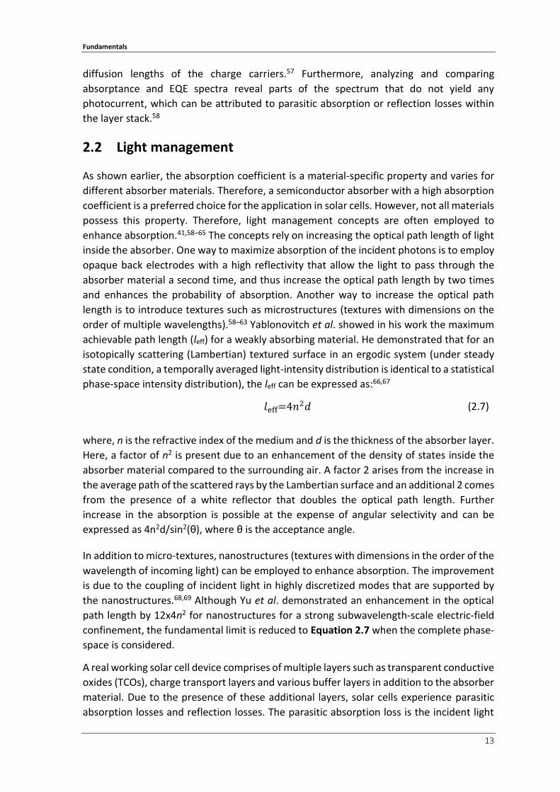
2.2 Light management ....................................................................................................... 13
2.3 Detailed balance limit of solar cells ............................................................................. 15
2.4 Tandem solar cells ........................................................................................................ 15
2.5 Perovskite solar cells .................................................................................................... 17
3. Methods and Characterizations ..................................................................................... 23
3.1 Fabrication and synthesis ............................................................................................. 24
3.1.1 Synthesis of TiO2 nanoparticles ........................................................................... 24
3.1.2 Sputtering technique ........................................................................................... 25
3.1.3 Fabrication of a typical perovskite solar cell........................................................ 27
3.1.4 Fabrication of nanostructured ITO ...................................................................... 33
3.2 Characterization Techniques ........................................................................................ 35
3.2.1 Electrical characterization.................................................................................... 36
3.2.2 Optical characterization ....................................................................................... 38
3.2.3 Material characterization .................................................................................... 41
4. Nanoparticle-based electron transport layers for semitransparent perovskite
solar cells ..................................................................................................................... 45
4.1 np-TiO2 ETL for perovskite solar cells ........................................................................... 47
4.1.1 Material properties of np-TiO2............................................................................. 47
4.1.2 Additional features of np-TiO2 ............................................................................. 49
4.1.3 Photovoltaic characteristics with np-TiO2 ............................................................ 52
4.2 np-SnO2 ETL for perovskite solar cells .......................................................................... 56
4.2.1 Material properties of np-SnO2 ........................................................................... 57
4.3 Comparison between np-TiO2 and np-SnO2 ETL .......................................................... 57
4.3.1 Optical properties, photo-physics and morphology ............................................ 57
4.3.2 Photovoltaic characteristics of PSCs with nanoparticle-based ETL ..................... 59
4.4 Discussions and conclusion .......................................................................................... 61
5. Nanophotonic electrodes for perovskite-based tandem photovoltaics ........................... 63
5.1 Periodic nanophotonic electrodes ............................................................................... 65
5.2 Disordered nanophotonic electrodes .......................................................................... 68
5.3 Photovoltaic characteristics of perovskite solar cells with nanostructured ITO.......... 71
5.3.1 Semitransparent perovskite and perovskite/c-Si tandem solar cells .................. 71
5.3.2 Nanostructured ITO and its potentials ................................................................ 74
5.3.3 Energy yield analysis for perovskite solar cells with NS ITO ................................ 77
5.4 Discussions and conclusion .......................................................................................... 80
6. Semitransparent perovskite solar cells for four-terminal tandem architectures .............. 83

6.1 Bandgap tuning of perovskite absorbers ..................................................................... 86
6.1.1 Material properties .............................................................................................. 87
6.1.2 Photovoltaic characteristics of perovskite solar cells for optimum bandgap ..... 89
6.2 Alternative transport conductive oxide electrodes ..................................................... 98
6.2.1 Rear TCOs for semitransparent perovskite solar cells ....................................... 100
6.2.2 Front TCOs for semitransparent perovskite solar cells ..................................... 102
6.3 Photovoltaic characteristics of perovskite solar cells with various TCOs .................. 106
6.4 Discussions and conclusion ........................................................................................ 111
7. Conclusion and outlook ............................................................................................... 113
7.1 Outlook ...................................................................................................................... 114
Appendix ......................................................................................................................... 117
References ...................................................................................................................... 126
List of publications and contributions to conferences ....................................................... 142
Peer-review publication (first author) ............................................................................... 142
Peer-reviewed publications (co-author) ........................................................................... 142
Submitted articles (co-author) .......................................................................................... 144
Contributions to conferences ............................................................................................ 144
Acknowledgements ......................................................................................................... 145


1
1. Introduction
Since pre-industrial times, earth’s surface temperature has increased by 1.0 °C.1 This is
primarily due to the burning of fossil fuels such as coal, natural gas and oil for electricity
and heat.2 Burning these natural resources releases carbon dioxide, methane and other
greenhouse gasses into the atmosphere that trap sun’s irradiation and increase overall
earth’s surface temperature.3 This rise in the temperature is already showing significant
effects such as the melting of the Arctic and Antarctic ice caps,1,4 which if not stopped,
could reshape out planet. Further consequences include an increase in the sea level, which
can have devastating effects on low-lying coastal wild-lives and habitats, impact on
biodiversity and ecosystem, ocean acidity, etc.1,5 Therefore, initiatives must be taken to
reduce our carbon footprint.6
Even with our climate under threat from greenhouse gasses, global electricity needs are
expected to increase.7 Projections estimate that by 2040, countries like China, India and
other developing nations will be the major consumer of electricity, while demand from
more developed nations remains fairly unchanged.7 Therefore, renewable sources such as
wind and solar must play a crucial role to provide the required electricity demand and
sustain the future of our earth. Today, solar energy contributes to only a small but
respectable fraction of the total electricity generation (3%), but the future electricity
demand requires it to become a major contributor of electricity.7 It is expected that by
2040, solar energy will surpass the global power generation capacity of both coal and gas.7
Meeting the energy demand in future will be challenging if sufficient development in the
solar energy technologies is not achieved with a focus on the economics of power
generation. Therefore, a reduction in the levelized cost of electricity (LCOE) is required,
which is defined as the average cost of electricity by a technology over its lifetime.
Although a strong economic viability of solar photovoltaic (PV) was shown in a report in
2018 for Germany,8 the LCOE can further be reduced by increasing the power conversion
efficiency (PCE) of solar cells. In this regard, a reduction in the LCOE could be limited for
the currently established silicon PV as its PCE is already very close to its fundamental limit.
One approach to surpass this is to combine highly efficient wide-bandgap semitransparent
perovskite solar cell (s-PSC) as a top cell in conjunction with a crystalline-silicon (c-Si) solar
cell as a bottom cell to form a tandem solar cell as shown in Fig. 1.1.
Perovskite PV is a thin-film based technology with perovskite crystals as the absorber
material. This PV technology has shown enormous progress9,10 and to date demonstrates
PCE > 25% in solution-processed opaque devices (Fig. 1.2).10 Additional advantages for
perovskite absorbers include feasibility of upscaling from laboratory small scale to large
areas via roll-to-roll processing,9,11 which can reduce the manufacturing cost. Furthermore,
owing to its wide bandgap feature, s-PSCs can be combined with a bottom solar cell in a
tandem architecture.12 In combination with c-Si solar cells, PCEs of perovskite-based
tandem devices have already surpassed the record PCE of a single-junction crystalline-
Introduction
2
silicon solar cell to date.10,13,14 Not only this has been shown for perovskite/c-Si solar cells
but also for perovskite/CIGS solar cells as well.10 However, there is still room for further
developments. The primary losses that currently limit the PCE are: (i) optical losses due to
reflections from various interfaces,15 parasitic absorptions within the layer stack,16 and
non-ideal bandgaps,14,17,18 (ii) non-radiative recombination losses occurring inside the bulk
or at the interfaces of the perovskite absorber layer,19–27 and poor extraction and transport
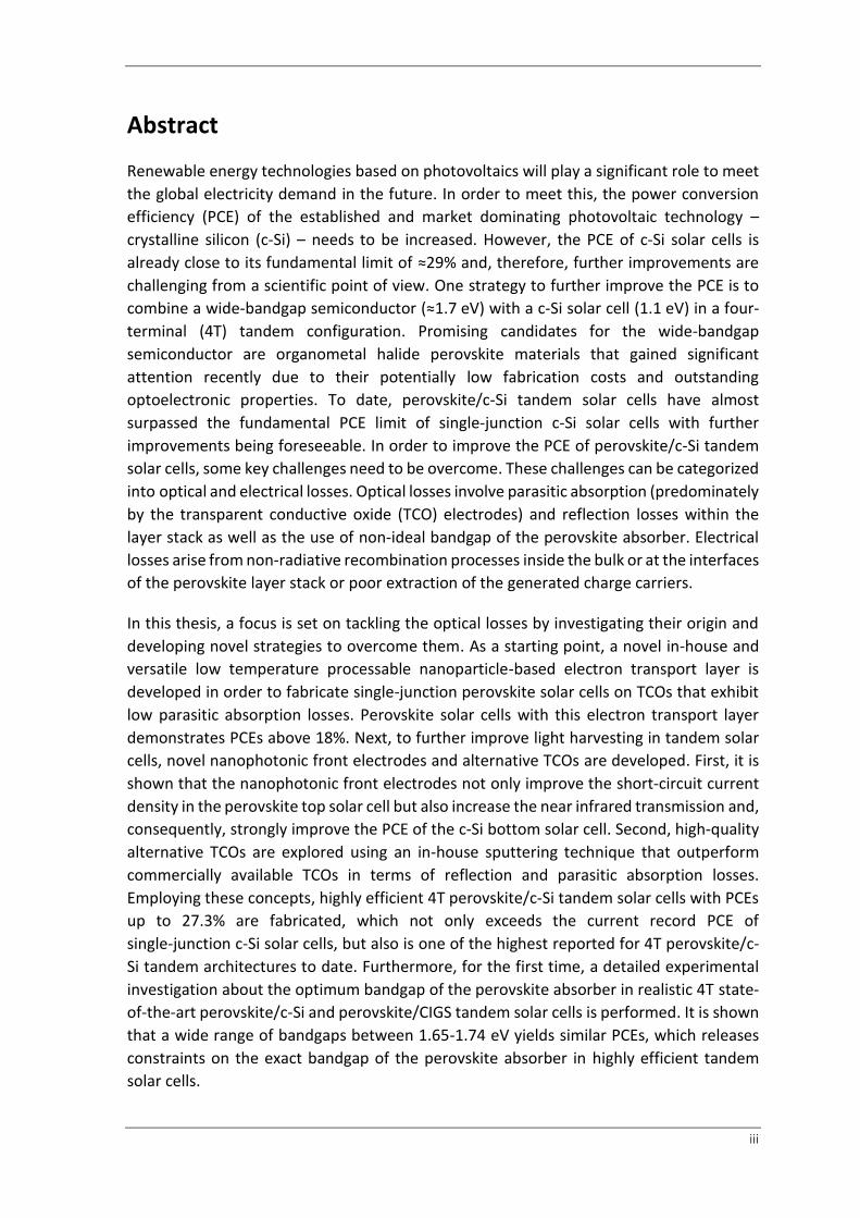
of charges by charge transport layers.28–30 Fig. 1.1 illustrates the various layers that are
responsible for some of these losses in a perovskite-based tandem device.
In regard to the extraction of electrons, PSCs conventionally use electron transport layers
(ETLs) comprising of mesoporous TiO2,28–35 which resulted in some of the highest PCEs for
opaque perovskite solar cells (o-PSCs).31–34 From an optical point of view for obtaining high
PCE in tandem architectures, mesoporous TiO2 is undesirable. Since it can only be
processed on fluorine-doped tin oxide (FTO) electrode, which is highly absorbing both in
the visible and in the near infrared wavelengths, it will result in reduced transmission in
s-PSCs and hence, loss in the PCE of tandem devices. The underlying reason of utilizing FTO
electrode is the requirement of a high annealing temperature (> 450 °C) that ensures
satisfactory layer quality of mesoporous TiO2 ETL.31–34 Because of this, transparent
conductive oxides (TCOs) that exhibit reduced parasitic absorption losses36,37 as well as
Fig. 1.1. Schematic representation of four-terminal tandem solar cell with semitransparent perovskite solar cell (s-PSC) as the top cell. High parasitic absorption and reflection losses lead to low transmission in a top s-PSC. Additional challenges include high temperature processed electron transport layer, non-optimum bandgap and high non-radiative recombination losses in the perovskite absorber.

Introduction
3
low-cost flexible plastic substrates required for future roll-to-roll processing, are not
compatible. Therefore, alternative ETLs must be investigated to overcome the limitations
of high temperature processing in this layer. Thus, in this thesis, the following research
question (RQ) is investigated:
RQ 1 – Can pre-synthesized nanoparticle-based TiO2 and SnO2 be used as an alternative
electron transport layer to fabricate efficient perovskite solar cells?
In order to improve the PCE in perovskite-based tandem devices, reflection and parasitic
absorption losses must be minimized. The prominent parasitic absorption loss in a top
s-PSC stems from the TCO electrodes (both front and rear).15,16,36–38 Reflection losses
originate from various interfaces that forms the tandem stack, however, a considerable
share is associated to the TCOs.39,40 Both absorption and reflection losses decrease the
transmission of the top s-PSCs, leading to a reduction in the PCE of the bottom solar cells
in tandem architectures and hence, an overall reduction in device PCE. Thus, further
investigations are required in the field of TCO electrodes to reduce these optical losses for
tandem PV. In this regard, light management with nanostructures – textures significantly
smaller than the wavelength of visible light – can be employed to reduce reflections and
improve transmission.41–43 Besides this, alternative materials can be explored that exhibit
reduced optical losses. Several materials show such properties, which would be beneficial
for perovskite-based tandem applications, if employed.36,37 Therefore, in order to reduce
these losses, this thesis investigates the following research question:
RQ 2 – What is the role of nanophotonic light management concepts or alternative
transparent conductive oxide electrodes in improving the PCE of perovskite-based tandem
devices?
Fig. 1.2. Efficiency chart of various solar energy technologies. Figure adapted from
NREL efficiency chart.10

Introduction
4
Another aspect which is highly important to consider both from optical and electrical point
of view for maximizing the PCE in a tandem device architecture is the optimum bandgap
of the perovskite absorber. In optical terms, detailed-balance calculations17,18 and energy
yield modelling44 suggest a wide-range of bandgaps are suitable for the top perovskite
absorber for maximizing the PCE in a perovskite-based four-terminal tandem device
architecture. A four-terminal tandem device implies that the top solar cell and the bottom
solar cell are optically connected as one device but can work independently (see
discussions in chapter 2, section 2.3 and 2.4 for more details). A bandgap between
1.60-1.85 eV is assumed to be the optimum for the top absorber in such a tandem device
(see Fig. 1.3). Only one experimental study regarding the optimum bandgap was carried
out for perovskite/CIGS tandem solar cells, the resultant net efficiencies of which, were
not reflected in their reported champion efficiency.45 From an electrical standpoint, one
needs to consider that widening the bandgap (> 1.73 eV) of the top perovskite absorber is
detrimental to device performance due to extensive non-radiative recombination
processes in such architectures,19–27 which are neglected in simulations. Therefore, a
detailed experimental investigation is necessary with real prototypes to examine the effect
of various bandgaps in the optimum range of the top perovskite absorber to maximize the
PCE in perovskite-based tandem solar cells. Thus, in this thesis, the following research
question is investigated:
RQ 3: What is the optimal bandgap of the perovskite absorber in the top s-PSC in real
prototype devices for maximizing the PCE of perovskite-based tandems?
Outline of the thesis
This introductory chapter is followed by chapter 2, which provides the reader with a review
of the fundamentals required to follow the content of this thesis. The chapter discusses
Fig. 1.3. Theoretical power conversion efficiency (PCE) as a function of top and bottom
sub-cell bandgap in four-terminal (4T) architecture without parasitic absorption or
transmission losses.

Introduction
5
the working principles governing single-junction and tandem solar cells. Furthermore, the
chapter outlines the material properties of perovskite absorbers and light management
within a solar cell.
In chapter 3, the various fabrication methods and the characterization tools used in this
thesis are introduced.
Chapter 4 deals with RQ 1 and presents a study for perovskite solar cells with two different
types of ETLs based on nanoparticles: TiO2 and SnO2. These nanoparticle-based ETLs are
deposited at a low temperature (up to 150 °C), enabling deposition on TCO electrodes with
low parasitic absorption losses. A comparative study between the two ETLs is also
presented in this chapter.
Chapter 5 deals with RQ 2. A nanophotonic light management concept is applied by nano
structuring TCOs to reduce reflection losses and to improve the PCE in perovskite/c-Si
tandem devices.
Chapter 6 presents further research in improving the performance of perovskite-based
tandem PV. In the first part of this chapter, a detailed experimental investigation is carried
out with real prototype devices to investigate RQ 3. In the second part, alternative TCO
electrodes are explored for investigating RQ 2 and improving the PCE in perovskite/c-Si
tandem devices.
In chapter 7, the key results of this thesis are summarized, and an outlook is presented.

Introduction
6
7
2. Fundamentals
This chapter discusses the fundamental working principle of solar cells. Furthermore, it
includes a brief introduction to perovskite solar cells, tandem architectures and light
management.
2.1 Working principle of solar cells
Semiconductor physics of a solar cell
While the photovoltaic market is dominated by crystalline silicon solar cells that employ a
p-n architecture, a wide range of solar cells with other architectures or layer sequences
exist in the literature.46–48 For instance, organic solar cells with bulk heterojunctions and
amorphous silicon solar cells employ a p-i-n layer sequence. The focus of this thesis which
is the perovskite solar cells (PSCs), also use the p-i-n layer sequence. In a p-i-n layer
sequence, an absorber layer (denoted by i) is sandwiched between a hole transport layer
(denoted by p) and an electron transport layer (denoted by n). Two electrodes, one of
which is at least optically transparent, are used to extract the photo-generated charge
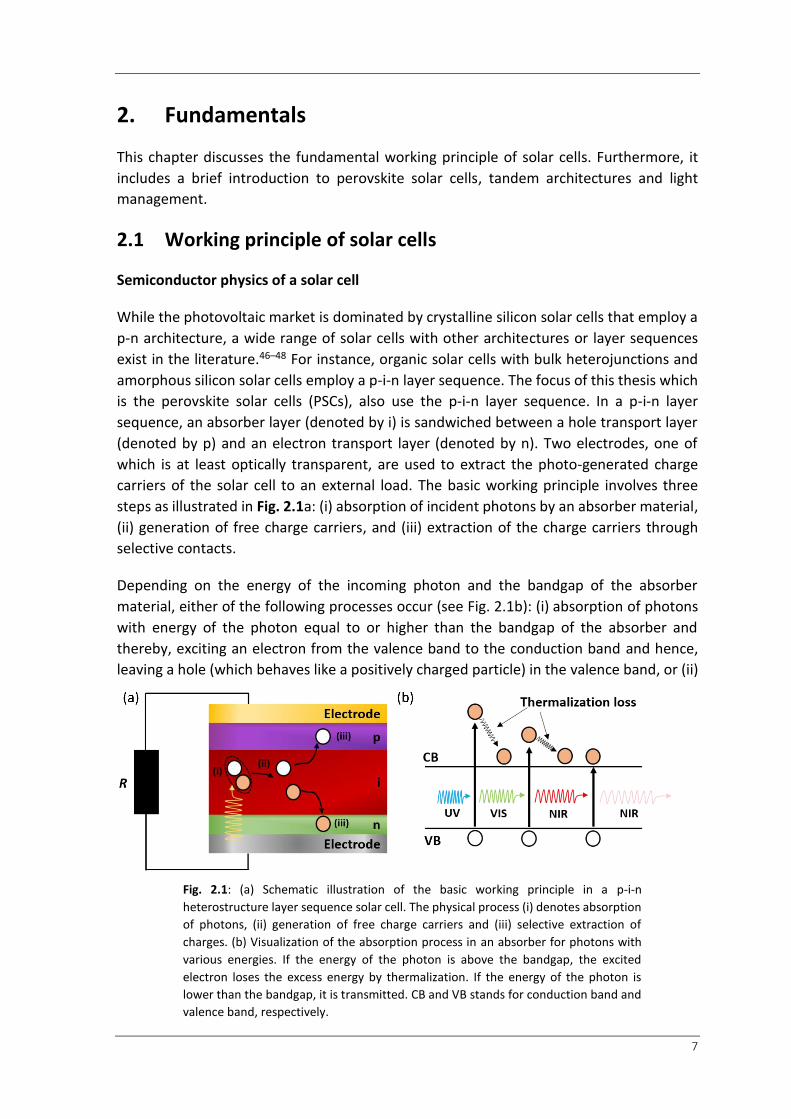
carriers of the solar cell to an external load. The basic working principle involves three
steps as illustrated in Fig. 2.1a: (i) absorption of incident photons by an absorber material,
(ii) generation of free charge carriers, and (iii) extraction of the charge carriers through
selective contacts.
Depending on the energy of the incoming photon and the bandgap of the absorber
material, either of the following processes occur (see Fig. 2.1b): (i) absorption of photons
with energy of the photon equal to or higher than the bandgap of the absorber and
thereby, exciting an electron from the valence band to the conduction band and hence,
leaving a hole (which behaves like a positively charged particle) in the valence band, or (ii)
Fig. 2.1: (a) Schematic illustration of the basic working principle in a p-i-n
heterostructure layer sequence solar cell. The physical process (i) denotes absorption
of photons, (ii) generation of free charge carriers and (iii) selective extraction of
charges. (b) Visualization of the absorption process in an absorber for photons with
various energies. If the energy of the photon is above the bandgap, the excited
electron loses the excess energy by thermalization. If the energy of the photon is
lower than the bandgap, it is transmitted. CB and VB stands for conduction band and
valence band, respectively.

Fundamentals
8
transmission of photons when their energy is lower than the bandgap. If the photon energy
exceeds than the bandgap, the excited electron in the conduction band undergoes a
subsequent relaxation to the edge of the conduction band through lattice vibrations
(phonons). This process is known as thermalization (see Fig. 2.1b for a comparison
between ultra-violet (UV), visible (VIS) and near infrared (NIR) radiations). This limits the
maximum energy harvested by each photon to the bandgap of the absorber material.
The absorption process also depends on the energy of the incoming photons. Higher
energy photons are absorbed within a short distance inside the absorber, while lower
energy photons are absorbed deeper inside the material (see absorption coefficient of a
typical perovskite film in Fig. 2.2). This implies that the thickness of the absorber should be
sufficiently large (especially for low energy photons) to maximize the absorption process.
To quantify the amount of light absorbed by an absorber for a given thickness, the Beer-
Lambert law is used:49
𝐼(𝐸, 𝑧) = 𝐼0𝑒−𝛼(𝐸)𝑧 (2.1)
where, I(E, z) is the intensity of light for a photon with certain energy (E) after propagating
a distance (z) inside the semiconductor and I0 is the incident intensity.
Subsequent to absorption, both electrons and holes can recombine, if not extracted. The
fundamental bulk recombination processes that exist in a typical solar cell are bimolecular
(radiative), Auger (non-radiative) and Shockley-Read-Hall recombination (non-radiative).
Both bimolecular radiative and Auger recombination are inevitable processes. Bimolecular
radiative recombination occurs when an electron recombines with a hole and emits a
photon. It is pronounced in direct bandgap semiconductors and light emitting diodes
(LEDs) rely on this mechanism. The Auger recombination requires high charge carrier
concentrations, which often exists due to heavy doping or high level injection under
Fig. 2.2: Absorption coefficients of a perovskite film and silicon absorber. The data are
obtained from references [211,212].

Fundamentals
9
concentrated sunlight. While in silicon solar cells operated under 1 sun conditions, Auger
recombination process is of relevance and sets the fundamental power conversion
efficiency limit, for perovskite solar cells, under such operating conditions, it is irrelevant
due to the presence of low charge carrier concentration. The Shockley-Read-Hall
recombination is a non-radiative trap-assisted recombination process and is governed by
defects present inside the bulk of the absorber layer. Thus, one of the main challenges for
fabricating highly efficient solar cells is to reduce defect densities and suppress the
Shockley-Read-Hall recombination. A key characteristic for the quality of an absorber is the
charge carrier diffusion length (ldiff), which denotes the average distance electrons and
holes diffuses in the semiconductor in between photo-generation of charge carriers and
recombination. Therefore, it is very essential to consider a smaller thickness of the
absorber to reduce the recombination processes for an efficient solar cell operation.
Therefore, given the conditions for maximizing the absorption as well as reducing the
recombination process, the thickness (t) of the absorber should be:
1/𝛼 < 𝑡 < 𝑙diff (2.2)
Typical charge carrier diffusion lengths for organometal halide perovskites are in the order
of several microns, whereas typical thicknesses of the absorber in perovskite solar cells is
only several hundred of nanometers.50 Thus, from this perspective, perovskite absorbers
are an excellent material for solar cell application.
Band diagram
Perovskite solar cells have a p-i-n heterostructure layer sequence but care must be taken
in order to understand its working principle. While conventional p-i-n (e.g. amorphous
silicon solar cells) solar cells exhibit both diffusion (due to the chemical potential) and drift
currents (due to the presence of a built-in voltage), the latter is less relevant for PSCs.
Fig. 2.3: Schematic illustrations of the band diagram in a p-i-n heterostructure
illuminated under (a) short-circuit and (b) at an operating condition. Schematics
adapted from [213]. Vbi stands for built-in voltage.

Fundamentals
10
Several studies have shown that a flat band scenario describes best the working principle
in PSCs,51,52 implying that the charge separation occurs mostly due to the presence of the
chemical potential, i.e., diffusion of charges. Furthermore, as discussed by Würfel et al. in
great detail, that it is the selectivity of the charge transport layers that plays the most
crucial role for an efficient charge separation, instead of the built-in voltage.53 The
selectivity is achieved by a large electron (hole) conductivity in the n-type (p-type) layer,
allowing electrons (holes) to flow easily while efficiently blocking holes (electrons). By
numerical simulations, Würfel et al. even demonstrated that a p-i-n (or n-i-p) solar cell
could be very efficient if there is no built-in voltage at all or if a small built-in voltage is
even opposing the diffusion of charge carries. Simplified schematics of the band diagram
for a flat band solar cell under illumination at short-circuit conditions and at operating
condition are illustrated in Fig. 2.3. Under continuous illumination and at short-circuit
conditions, the fermi energy (EF) stays constant throughout the device and the additional
photo-generated electrons and holes are efficiently extracted by the contact layers (Fig.
2.3a), simply by introducing sufficiently high band offsets. At this condition, a net current
(Iph) flows through the device. Under continuous illumination and at an operating
condition, the Fermi energy splits into quasi-Fermi levels for electrons residing at energy
EF,e and holes at energy EF,h with EF,e and EF,h aligning with the Fermi levels of the n-type
and p-type layers, respectively (Fig. 2.3b). At this condition, both voltage and current are
generated simultaneously by the solar cell and a power is delivered.
Characteristics of a solar cell
The operating principle of a solar cell can be represented by a simple one-diode or two-
diode model (Fig. 2.4a,b). The photocurrent is represented by a current source in parallel
to one or two diodes with a series resistance (Rs) and a shunt resistance (Rsh). The presence
of Rs is due to the fact that the photogenerated charges experience some resistances as
they are injected in their selective contacts, and transported through the transport layers
and the electrodes. The Rsh arises when the photogenerated charges flow within the device
through grain boundaries, defects or direct contact between the two electrodes. Such
losses are represented by a current (Ish) flowing through a parallel or shunt resistance. The
simple one-diode model can already effectively describe behavior of good solar cells.
However, the two-diode model can result in a further description of experimental data as
it includes the recombination mechanisms of the charge carriers as well. The relation
between the net current I and the voltage V is given by the Shockley equation:49
Fig. 2.4: Schematic illustration of (a) one-diode and (b) two-diode model of a solar
cell.

Fundamentals
11
𝐼(𝑉) = 𝐼0𝑒
𝑞𝑉𝑘𝐵𝑇
−1− 𝐼𝑝ℎ
(2.3)
where, I0 is the dark saturation current, q is the charge of an electron, kB is the Boltzmann
constant, V is the voltage, Iph is the photocurrent and T is the temperature of the solar cell.
The performance of a solar cell is determined from its I-V characteristics. Fig. 2.5 shows a
typical I-V curve and the output power (P) of a solar cell. The I-V characteristic curve follows
the same pattern similar to a diode with an offset of ISC. As the voltage increases from
short-circuit condition (V = 0 V), power (P = IV) delivered by the solar cell increases until it
maximizes. This is defined as the maximum power point (MPP) of the solar cell. At this
point, the current flowing through the device is I = IMPP at a voltage V = VMPP, resulting a
power PMPP = IMPP x VMPP. Further increase in the voltage reduces the output Iph as the
current through the diode, Id, increases. As a result, P decreases. At open-circuit condition,
Iph = Id and the P is zero. In order to maximize the power conversion efficiency (PCE) in real
solar cells or solar modules, a PID controller is equipped in a feedback loop such that the
device always operates close to the MPP. The area under the I-V characteristics or the ratio
between PMPP to the ISC and VOC is defined as the fill factor (FF) of a solar cell and is given
by:49
𝐹𝐹 =
𝑃𝑀𝑃𝑃
𝐼𝑆𝐶 . 𝑉𝑂𝐶
(2.4)
Both Rs and Rsh influence the FF of a solar cell. Ideally, in order to maximize FF, the Rs and
Rsh should be low and high, respectively. The PCE of a solar cell can then be represented
as:49
Fig. 2.5: (a) Current-voltage (I-V) characteristic curve and (b) power dependency of a
typical silicon solar cell. At voltage V = 0, the current flowing through the solar cell is
short-circuit current, ISC. At current I = 0, the voltage across the solar cell is the open-
circuit voltage, VOC. Both at I = ISC and V = VOC, the output power P = 0. The output
power maximizes at the maximum power point where I = IMPP and V = VMPP.

Fundamentals
12
PCE =
𝐼𝑆𝐶 . 𝑉𝑂𝐶 . 𝐹𝐹
𝑃𝑖𝑛𝑝𝑢𝑡
(2.4)
where, Pinput is the incident power of light. Under standardized test condition, an
irradiation of 1000 Wm-2 with an AM 1.5G (air mass global, optical path length = 1.5 times
earth’s atmosphere, obtained using a solar simulator) spectrum at 25 °C is considered as
the incident power.54 The AM 1.5G irradiation spectrum includes optical absorptions due
to atmospheric gases such as ozone, carbon dioxide and water vapor and represents the
optical path length that the sun’s irradiation has crossed the atmosphere considering an
incident angle of 48.2° to the northern hemisphere.54
While solar simulator presents the overall performance of a solar cell under simulated
AM 1.5G irradiation spectrum, external quantum efficiency (EQE) measurements show the
spectrally resolved response of the solar cell (Fig. 2.6). It is defined as the ratio between
number of extracted electron-hole pairs (Ne,h) to the number of incident photons (Np(λ)):
EQE(λ)=
d𝑁e,h(λ)
d𝑁p(λ)=
1
e d𝐽sc(λ)
dϕγ(λ)
(2.5)
where, ϕγ(λ) is the photon flux per unit area at wavelength (λ) and JSC(λ) is the short-
circuit current density. Integrating equation 2.5 weighted by the photon flux yields the
short-circuit current density of a solar cell and is given by:55
𝐽sc= e ∫ EQE(λ)ϕ(λ)dλ
∞
0
(2.6)
Analysis of EQE spectra provide more information than just the JSC. For example, surface
recombination and amount of parasitic absorption losses in a solar cell can also be
estimated. A weak EQE in the short wavelengths indicates front surface recombination,56
while a weak EQE in the long wavelengths indicates incomplete absorption or too short
Fig. 2.6: External quantum efficiency of a typical perovskite solar cell.
Fundamentals
13
diffusion lengths of the charge carriers.57 Furthermore, analyzing and comparing
absorptance and EQE spectra reveal parts of the spectrum that do not yield any
photocurrent, which can be attributed to parasitic absorption or reflection losses within
the layer stack.58
2.2 Light management
As shown earlier, the absorption coefficient is a material-specific property and varies for
different absorber materials. Therefore, a semiconductor absorber with a high absorption
coefficient is a preferred choice for the application in solar cells. However, not all materials
possess this property. Therefore, light management concepts are often employed to
enhance absorption.41,58–65 The concepts rely on increasing the optical path length of light
inside the absorber. One way to maximize absorption of the incident photons is to employ
opaque back electrodes with a high reflectivity that allow the light to pass through the
absorber material a second time, and thus increase the optical path length by two times
and enhances the probability of absorption. Another way to increase the optical path
length is to introduce textures such as microstructures (textures with dimensions on the
order of multiple wavelengths).58–63 Yablonovitch et al. showed in his work the maximum
achievable path length (leff) for a weakly absorbing material. He demonstrated that for an
isotopically scattering (Lambertian) textured surface in an ergodic system (under steady
state condition, a temporally averaged light-intensity distribution is identical to a statistical
phase-space intensity distribution), the leff can be expressed as:66,67
𝑙eff=4𝑛2𝑑 (2.7)
where, n is the refractive index of the medium and d is the thickness of the absorber layer.
Here, a factor of n2 is present due to an enhancement of the density of states inside the
absorber material compared to the surrounding air. A factor 2 arises from the increase in
the average path of the scattered rays by the Lambertian surface and an additional 2 comes
from the presence of a white reflector that doubles the optical path length. Further
increase in the absorption is possible at the expense of angular selectivity and can be
expressed as 4n2d/sin2(θ), where θ is the acceptance angle.
In addition to micro-textures, nanostructures (textures with dimensions in the order of the
wavelength of incoming light) can be employed to enhance absorption. The improvement
is due to the coupling of incident light in highly discretized modes that are supported by
the nanostructures.68,69 Although Yu et al. demonstrated an enhancement in the optical
path length by 12x4n2 for nanostructures for a strong subwavelength-scale electric-field
confinement, the fundamental limit is reduced to Equation 2.7 when the complete phase-
space is considered.
A real working solar cell device comprises of multiple layers such as transparent conductive
oxides (TCOs), charge transport layers and various buffer layers in addition to the absorber
material. Due to the presence of these additional layers, solar cells experience parasitic
absorption losses and reflection losses. The parasitic absorption loss is the incident light

Fundamentals
14
that is absorbed by other layers inside a solar cell stack and results in a loss of the
photocurrent. Therefore, TCOs15,36,37 with low near infrared absorptions and various
charge transport layers28–30,70 with wide bandgaps are preferred in solar cells in order to
reduce such parasitic absorption losses. The reflection losses originate from the difference
in the refractive indices of two adjacent layers in the solar cell stack. The reflectance (R)
between two adjacent layers is given by:
𝑅 = (
𝑛1 − 𝑛2
𝑛1 + 𝑛2)
2
(2.8)
where, n1 and n2 are the refractive indices of the two layers, respectively. Thus, a high
contrast between two adjacent layers leads to an increased reflection loss. In order to
reduce reflection losses, anti-reflection coatings (ARCs) are used in solar cells. These layers
could be a single-layer coating or multilayer.58,66 While single-layer ARCs are limited to a
small range of wavelengths and strongly sensitive to incident angles, multilayer coatings
can extend this range.59 The principle of an ARC relies on the destructive interference of
the reflected light. The thickness, d is given by:
𝑑=𝑚 (
λ
4𝑛)
(2.9)
where, n is the refractive index of the anti-reflection layer and λ is the wavelength. Other
strategies to reduce reflection losses involve micro- and nano-texturing. Micro-textures
scatter light by multiple reflections at its surface, and thereby, increases the probability of
light in-coupling and hence, reduces reflection losses (see Fig. 2.7a).38,59,61 The
nanotextures, in which the dimension of the structures are smaller than the wavelength
of the incident light, behaves like a gradient index film, and forms a so called effective
refractive index medium.41,71,72 Thereby, a gradual change in refractive index is achieved,
which reduces reflections and therefore, improves light in-coupling (see Fig. 2.7b). Further
details regarding parasitic losses and reflection losses due to the TCOs in perovskite solar
cells are discussed in section 2.5.
Fig. 2.7: Schematics of (a) micro-textures and (b) nano-textures for reducing reflection
losses. The micro-textures enable light in-coupling by multiple reflections at its
surface while nano-textures forms a so called effective refractive index medium.

Fundamentals
15
2.3 Detailed balance limit of solar cells
The maximum theoretical efficiency of a solar cell with an absorber bandgap, Eg, is
determined by the detailed balance limit. It was first proposed by Shockley and Queisser
in 1961 and therefore, the maximum PCE for a certain bandgap material is typically called
the Shockley-Queisser limit of a solar cell.73 The model assumes a blackbody irradiation
and calculates the PCE of a solar cell assuming:
(i) absorptance = 100%, for photons with hν > Eg;
(ii) absorptance = 0, for photons with hν < Eg;
(iii) one photon generates one electron-hole pair generation;
(iv) perfect collection, i.e., external quantum efficiency of 100%,
where, hν is the energy of the photon. The maximum PCE in a single-junction solar cell is
30% and is attained for a bandgap of ≈1.1 eV. However, considering an AM 1.5G irradiance
spectrum, the maximum PCE that can be attained by a single-junction solar cell is ≈33% for
a bandgap of 1.34 eV.74 In a follow-up study, De Vos calculated the fundamental efficiency
limit of a tandem solar cell in 1979.75 A tandem solar cell is a multi-junction solar cell with
two or more sub cells with various bandgaps. This study showed that an optimum bandgap
exists for each sub cell in a two-cell tandem device. Considering the same assumptions as
Shockley and Queisser, a maximum PCE of 42.3% is obtained with a top cell bandgap of 1.9
eV and a bottom cell bandgap of 1.0 eV. Simulating a two-cell tandem device for AM 1.5G
irradiation spectrum, even a higher PCE > 45% can be obtained for a wide range bandgap
as shown in chapter 1, Fig. 1.2. Further details regarding the working principle of a tandem
solar cell are discussed in the follow up section 2.4.
2.4 Tandem solar cells
Operating principle of a tandem solar cell
The foremost reason for the efficiency limit (≈33%) of a single-junction solar cell is the
bandgap of the absorber that limits the VOC, as higher energy photons always undergo
significant thermalization losses (Fig. 2.1b). One way to overcome this is to use a tandem
architecture as shown in Fig. 2.8a. The exemplary illustration shows a top cell with a wider
bandgap (Eg1 = 1.55 eV) absorber stacked on top of a bottom cell with a smaller bandgap
(Eg2 = 1.1 eV) material. Thus, photons with higher energies (hν > Eg1) are absorbed and with
smaller energies (hν < Eg2) are transmitted by the top cell. The transmitted photons are
absorbed by a bottom cell. As a result, the thermalization losses are reduced compared to
a single-junction and the PCE of the tandem device is increased and as already discussed
in section 2.3, the maximum theoretical PCE surpasses 45% for a tandem architecture.

Fundamentals
16
A critical requirement in a tandem solar cell architecture is to find the optimum bandgaps
of the top and the bottom solar cells. Arbitrary bandgaps will not maximize the PCE, rather
optimum bandgaps (Eg1 ≈1.80 eV, Eg2 ≈1.0 eV)17,18 for the two sub cells are required as
shown before in chapter 1, Fig. 1.2. Similar trends are also demonstrated in energy yield
studies, which estimate the power generated by a solar cell over a period of one year
depending on the weather and location44,76,77 As a bottom cell, Si is an excellent choice, as
the bandgap of Si is very close to the optimum bandgap of the bottom cell.13,34,63,78,79
However, other technologies exist today such as CIGS34,36,80 and low bandgap perovskites
(in lab scale).81,82 For the top cell, perovskite semiconductors are an excellent choice (see
section 3.6) as it can be deposited as a wide-bandgap semiconductor (already
demonstrated PCEs > 25%10 in opaque devices) and offers bandgap tunability.83,84 Further
details regarding the influence of the bandgap in a top perovskite solar cell for a tandem
architecture is discussed in Chapter 6.
Tandem solar cell architecture
The most common tandem configurations are a two-terminal (2T),63,78–80 or a four-terminal
(4T) architecture.13,14,34,81,82 In the 2T architecture, both sub cells cells are monolithically
connected, while in the 4T architecture, the two sub cells are mechanically stacked
(Fig. 2.9). Each architecture offers its own advantages and disadvantages. The 2T
architecture requires only one TCO layer, which reduces parasitic absorption losses.
However, it also implies a series connection of both sub cells, which requires current
matching of both sub cells to maximize the PCE and, in turn, imposes shortcomings to the
bandgap combinations.18,78,85 Only a narrow range of bandgaps can maximize the PCE. The
4T architecture allows each sub cell to operate independently at their MPPs and the
constraints in the fabrication of the sub cell are less as each sub cells can be fabricated
Fig. 2.8: (a) Schematic illustration of a tandem solar cell with two sub cells: top solar cell of Eg1 and bottom solar cell of Eg2 and (b) corresponding absorption of the irradiance spectrum AM 1.5G. The top solar cell absorbs photons up to 800 nm. The bottom solar cell absorbs the transmitted photons beyond 800 nm up to its bandgap.

Fundamentals
17
independently. Furthermore, since current matching is not crucial, the limitation on the
top solar cell absorber’s bandgap is reduced.18,44 As a result, a wide range of bandgaps
(1.60-1.85 eV) are suitable for this configuration. Nevertheless, this configuration requires
additional electrical equipment such as two inverters instead of one, which can effectively
increase the LCOE. Furthermore, since the two sub cells are optically connected,
intermediate index matching layers are required to reduce the optical losses.38 Moreover,
it is difficult to minimize parasitic absorption in this architecture as additional TCO
electrodes, charge transport layers and optical spacer are used.
2.5 Perovskite solar cells
Crystallography of perovskite
Perovskites are materials with a general chemical formula of ABX3. The basic crystal
structure consists of a unit cell with A, B and X atoms residing at the corners, at the center
and at the facets of the cube, respectively (Fig. 2.10).86 Besides the cubic phase, there are
other phases such as tetragonal or orthorhombic, the formation of which depends highly
on the temperature86,87 and stoichiometry.86 In an organometal halide perovskite crystal,
A is a monovalent cation (such as methyl ammonium: CH3NH3; formamidinium: CH3NH2;
cesium: Cs+; etc.), B is a divalent metal cation (such as lead: Pb2+; tin: Sn2+), and X is a
halogen (such as chloride: Cl-; bromide: Br-; iodide: I-). To determine if a certain
composition exhibits a stable crystal structure, the Goldsmith’s tolerance factor (t)88 serves
as an estimation and can be calculated using the following relation:
𝑡=
𝑟𝐴 + 𝑟𝐵
√2(𝑟𝐵 + 𝑟𝑋)
(2.7)
Fig. 2.9: Schematic illustrations of a (a) two-terminal (2T) tandem architecture and (b) four-terminal (4T) tandem architecture. In 2T architecture, both sub cells are monolithically interconnected. In 4T architecture, both sub cells are optically interconnected and can work independently.

Fundamentals
18
where, rA, rB, and rX are the ionic radii of the respective atoms. A stable cubic crystal
structure is typically formed when t is within the range 0.9<t<1.0.86 The most widely
investigated perovskite material for solar cells is methyl ammonium lead iodide (MAPI),
with the chemical formula CH3NH3PbI3 and has a tolerance factor of 0.91.89 Recent studies
show that replacing CH3NH3 with CH3NH2 and a certain amount of Cs+ can greatly improve
the tolerance factor (close to 1) and enhance the stability of the material.86 If the size of
the A atoms is beyond the limit of the tolerance factor such that a cation cannot fit inside
the cubic lattice, a 2D or quasi-2D perovskite is formed instead of a bulk 3D structure. This
structure can either be a Ruddelsen-Popper90,91 or Dion-Jacobson92 phase of the perovskite
absorber. Examples of such molecules for PSC applications are butyl ammonium,91
phenylethylammonium,93 iso-butylammonium,13,94 1,3-propanediamine (PDA),92 etc.
These molecules improve the stability of the absorber due to the presence of long
hydrophobic chains,95 or strong hydrogen bonding.92
Properties of metal-halide perovskite absorbers
Perovskite absorbers exhibit material properties that are highly suitable for solar cell
application. This includes a high absorption coefficient,96 high charge carrier mobilities,97
a low bimolecular recombination rate,97 long diffusion lengths50 and tunable bandgaps.83,84
A sharp absorption onset is present in perovskite absorbers due to the direct nature of the
bandgap.96 Therefore, for fabricating PSCs, thicknesses of ≈300-400 nm are sufficient for
absorbing most of the incident light. Along with sharp optical absorption edge, these
perovskite absorbers also present high charge carrier mobilities of ≈10 cm2 V-1 s-1 and a
low bimolecular recombination.97 Therefore, long diffusion length of the charge carriers,
exceeding 1 µm, have been observed in perovskites.50 Furthermore, the bandgap of the
absorber can be varied by tuning the composition of the material.83,84,98 By replacing iodide
with bromide in lead based perovskite absorbers, the bandgap can be tuned between
1.5-2.3 eV. This is due to the fact that when smaller bromide ions replace iodide ions, the
Fig. 2.10: Schematic illustration of the cubic phase crystal structure of a
perovskite absorber.
Fundamentals
19
lattice constant of the crystal structure is decreased and thereby, resulting an increase in
the bandgap. On the other hand, replacing the divalent cation lead with tin, lower
bandgaps (1.1 eV to 1.4 eV) are achieved.82 This makes perovskite absorber an interesting
material for various applications such as in tandem photovoltaics,99 lasers84 and LEDs.100
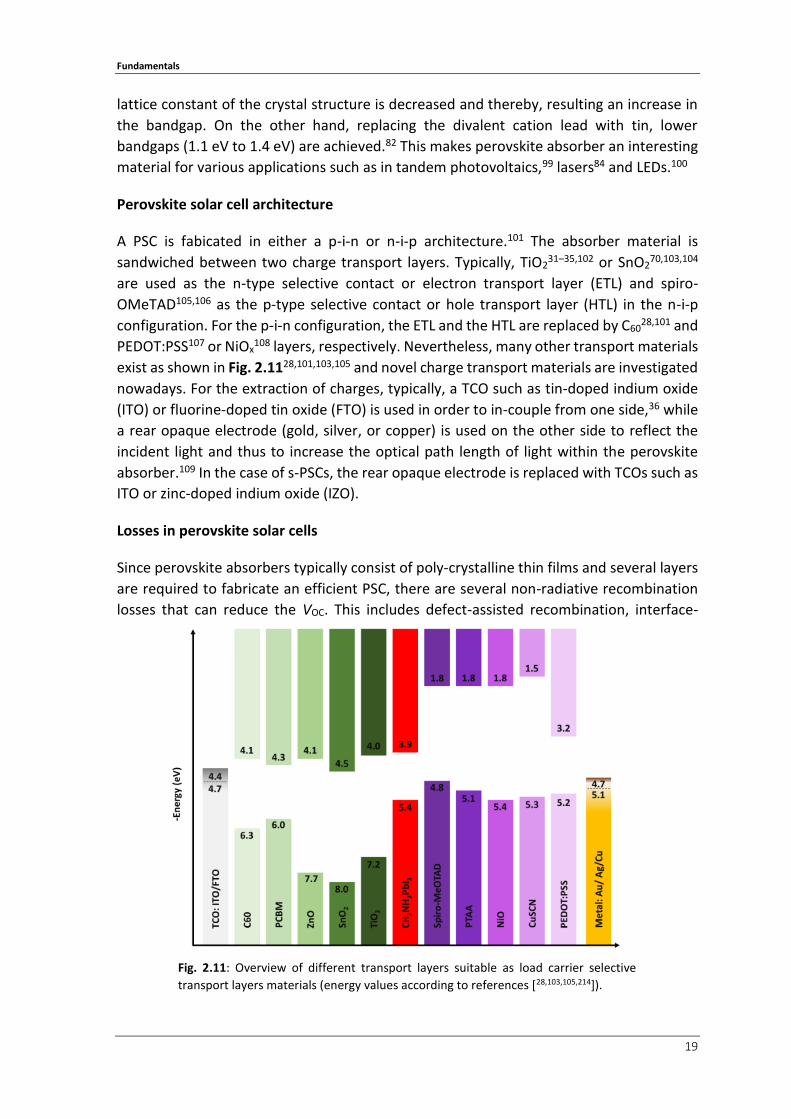
Perovskite solar cell architecture
A PSC is fabicated in either a p-i-n or n-i-p architecture.101 The absorber material is
sandwiched between two charge transport layers. Typically, TiO231–35,102 or SnO2
70,103,104
are used as the n-type selective contact or electron transport layer (ETL) and spiro-
OMeTAD105,106 as the p-type selective contact or hole transport layer (HTL) in the n-i-p
configuration. For the p-i-n configuration, the ETL and the HTL are replaced by C6028,101 and
PEDOT:PSS107 or NiOx108 layers, respectively. Nevertheless, many other transport materials
exist as shown in Fig. 2.1128,101,103,105 and novel charge transport materials are investigated
nowadays. For the extraction of charges, typically, a TCO such as tin-doped indium oxide
(ITO) or fluorine-doped tin oxide (FTO) is used in order to in-couple from one side,36 while
a rear opaque electrode (gold, silver, or copper) is used on the other side to reflect the
incident light and thus to increase the optical path length of light within the perovskite
absorber.109 In the case of s-PSCs, the rear opaque electrode is replaced with TCOs such as
ITO or zinc-doped indium oxide (IZO).
Losses in perovskite solar cells
Since perovskite absorbers typically consist of poly-crystalline thin films and several layers
are required to fabricate an efficient PSC, there are several non-radiative recombination
losses that can reduce the VOC. This includes defect-assisted recombination, interface-
Fig. 2.11: Overview of different transport layers suitable as load carrier selective
transport layers materials (energy values according to references [28,103,105,214]).
Fundamentals
20
induced recombination and band-tail recombination.110–117 The defect-assisted
recombination originates mainly from point defects such as interstitials, vacancies, and
antisites.110–112 These defects are nearly either positively or negatively charged, as they
have either holes or electrons localized in their vicinity. The interface-induced
recombination arises from the mismatch of energy levels, surface defects, and charge-
carrier back transfer.113–117 Such defects can block transfer of charges or cause band
bending near the contacts, resulting in increased non-radiative recombination. Overall,
these recombination losses reduce the VOC in a PSC. Another commonly known
experienced phenomenon that exists in a PSC is hysteresis.118,119 This arises due to the ion
migration and in the presence of electronic charge traps. The probable reason in the origin
of ion migration is the iodide ions in the perovskite absorbers, that exhibit low activation
energies. Furthermore, these mobile ions can accumulate at the interface and since they
act as traps, can further increase non-radiative recombination.120 The effect of these can
be observed in the J-V characteristics as a difference in the forward and reverse scan. The
hysteresis index (HI) is calculated using the following relation:
𝐻𝐼 =
𝐴𝑟𝑒𝑎 𝑢𝑛𝑑𝑒𝑟 𝐹𝑊 𝑠𝑐𝑎𝑛
𝐴𝑟𝑒𝑎 𝑢𝑛𝑑𝑒𝑟 𝐵𝑊 𝑠𝑐𝑎𝑛
(2.8)
where, FW and BW are the forward and backward scans, respectively. An HI of 1 implies
no hysteresis. Hysteresis in the J-V characteristics may lead to an over- or under-estimation
of the solar cell PCE. Therefore, a commonly established protocol followed by the research
community is to report device performance under a voltage at or close to the MPP.121
Stability of perovskite solar cells
PSCs are yet to overcome one of its prime challenges for future commercialization, i.e., the
poor stability, which can be ascribed to intrinsic material instability in the presence of
moisture, ultra-violet radiation and thermal stress.89,122–125 The moisture related instability
is mainly due to the hygroscopic nature of the amine group, that leads to an irreparable
damage of the perovskite, forming lead iodide and methylamine.123 The ultra-violet
degradation is mostly prominent in TiO2 based PSCs89 and arises from the light-induced
desorption of surface-adsorbed oxygen.124 Next to the ultra-violet instability, perovskite
absorbers are sensitive to thermal stress. With increasing temperature, MAPI shows a
degradation by releasing methyl ammonium iodide in the gas phase and leaving behind
PbI2.125 In recent years, several strategies have been undertaken to improve the stability
of the perovskite absorber showing promising stability of up to 1000 hours under
continuous operation. This includes optimization of the stoichiometry by including Cs
forming double or triple cation perovskite absorber,32 as well as the use of 2D
perovskites,126,127 and novel charge transport layers.128
Fundamentals
21
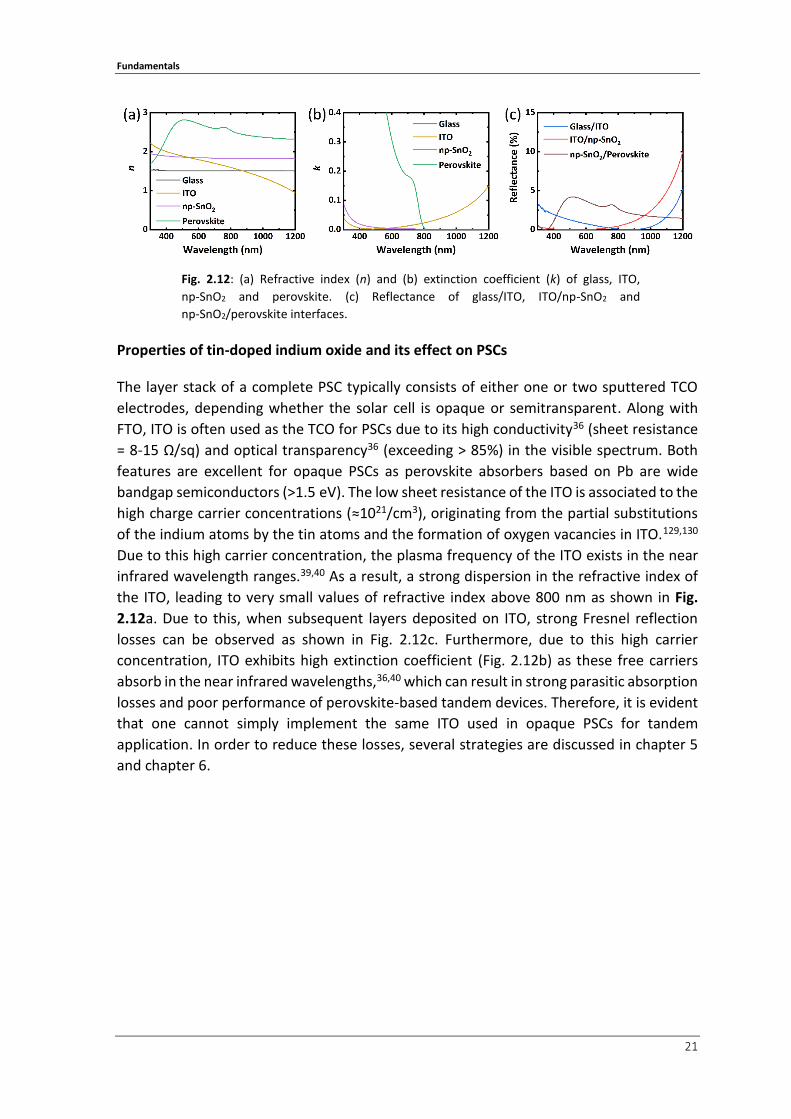
Properties of tin-doped indium oxide and its effect on PSCs
The layer stack of a complete PSC typically consists of either one or two sputtered TCO
electrodes, depending whether the solar cell is opaque or semitransparent. Along with
FTO, ITO is often used as the TCO for PSCs due to its high conductivity36 (sheet resistance
= 8-15 Ω/sq) and optical transparency36 (exceeding > 85%) in the visible spectrum. Both
features are excellent for opaque PSCs as perovskite absorbers based on Pb are wide
bandgap semiconductors (>1.5 eV). The low sheet resistance of the ITO is associated to the
high charge carrier concentrations (≈1021/cm3), originating from the partial substitutions
of the indium atoms by the tin atoms and the formation of oxygen vacancies in ITO.129,130
Due to this high carrier concentration, the plasma frequency of the ITO exists in the near
infrared wavelength ranges.39,40 As a result, a strong dispersion in the refractive index of
the ITO, leading to very small values of refractive index above 800 nm as shown in Fig.
2.12a. Due to this, when subsequent layers deposited on ITO, strong Fresnel reflection
losses can be observed as shown in Fig. 2.12c. Furthermore, due to this high carrier
concentration, ITO exhibits high extinction coefficient (Fig. 2.12b) as these free carriers
absorb in the near infrared wavelengths,36,40 which can result in strong parasitic absorption
losses and poor performance of perovskite-based tandem devices. Therefore, it is evident
that one cannot simply implement the same ITO used in opaque PSCs for tandem
application. In order to reduce these losses, several strategies are discussed in chapter 5
and chapter 6.
Fig. 2.12: (a) Refractive index (n) and (b) extinction coefficient (k) of glass, ITO,
np-SnO2 and perovskite. (c) Reflectance of glass/ITO, ITO/np-SnO2 and
np-SnO2/perovskite interfaces.

Fundamentals
22

23
3. Methods and Characterizations
This chapter discusses all the applied methods for the fabrication of a typical perovskite
solar cell (PSC) used in this thesis, deposition of planar and nanostructured transparent
conductive oxide (TCO) electrodes and synthesis of nanoparticles of titanium dioxide
(np-TiO2) electron transport layer (ETL). The chapter also outlines the techniques used to
characterize the fabricated devices and materials.
Acknowledgments and contributions
The major part of the experiments carried out for thesis is conducted by Ihteaz M. Hossain.
Ihteaz M. Hossain also acknowledges the support of Moritz Schultes for providing IO:H
substrates, Fabian Schackmar and Florian Mathies for inkjet printing of np-TiO2, Saba
Gharibzadeh for preparation of double cation perovskite absorber layers, Katharina Goth
for fabricating periodic nanostructured ITO samples, Yidenekachew J. Donie and Mohamed
S. Adbelkhalik for disordered nanostructured ITO, Isabel Allegro for AFM measurements,
David Ritzer for patterning TCOs and Michael Bruns XPS measurements.

Methods and Characterizations
24
3.1 Fabrication and synthesis
In this section, the methods used to fabricate perovskite solar cells (PSCs), nanostructured
ITO (NS ITO), sputter various transparent conductive oxides (TCOs) and synthesize
nanoparticles of TiO2 (np-TiO2) are discussed in detail.
3.1.1 Synthesis of TiO2 nanoparticles
This section describes the synthesis of the np-TiO2. A schematic of the synthesis process is
illustrated in Fig. 3.1. The synthesis process comprises of three critical steps: (i) a non-
hydrolytic sol-gel synthesis of np-TiO2, (ii) extraction and purification of the np-TiO2, and
(iii) dispersing in a suitable solvent.
The following precursor materials are required for the syntheses of np-TiO2:
(i) Titanium (IV) chloride, TiCl4 (Acros Organics)
(ii) Niobium (V) chloride, NbCl5 (Alfa Aesar)
(iii) Anhydrous ethanol, EtOH (Acros Organics)
(iv) Benzyl alcohol, BnOH (Acros Organics)
(v) Diethyl ether, Et2O (Honey well)
(vi) Diethylene glycol monoethyl ether, DEGEE (Sigma Aldrich)
(vii) 1-butanol (Sigma Aldrich)
(viii) Titanium diisopropoxide bis acetonyl acetate, Ti(O-iPr)2(acac)2 (Sigma Aldrich)
In the first step of the synthesis of undoped np-TiO2, 4.5 mmol of TiCl4 is added dropwise
to 2 ml of EtOH in a glass vial. In order to synthesize the np-TiO2 doped with Nb5+ for
improved conductivity, TiCl4 is added to a 0.17 M solution of NbCl5 dissolved in EtOH. This
Fig. 3.1: Schematic illustration of the nanoparticles of TiO2 synthesis. The three main
steps of the synthesis process are: (i) non-hydrolytic sol-gel synthesis of np-TiO2, (ii)
extraction and purification of the np-TiO2, and (iii) dispersing in a suitable solvent.
Reproduced with permission from ACS Applied Energy Materials,[139] © American
Chemical Society.
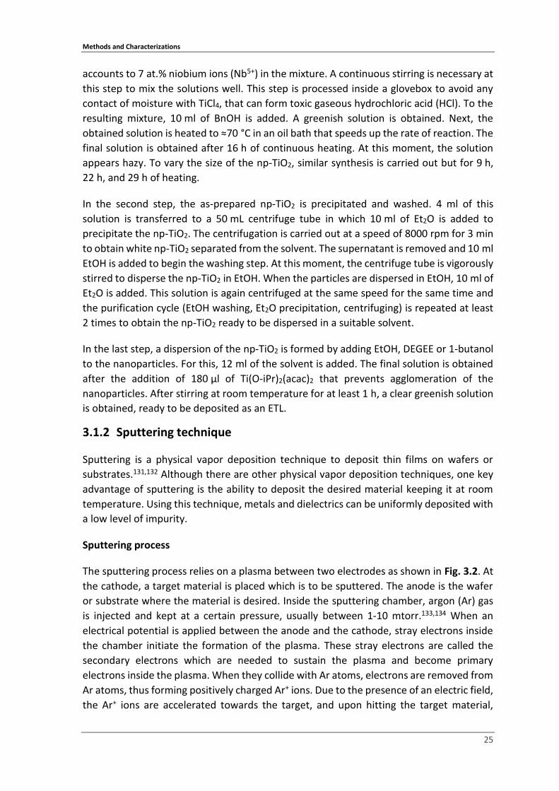
Methods and Characterizations
25
accounts to 7 at.% niobium ions (Nb5+) in the mixture. A continuous stirring is necessary at
this step to mix the solutions well. This step is processed inside a glovebox to avoid any
contact of moisture with TiCl4, that can form toxic gaseous hydrochloric acid (HCl). To the
resulting mixture, 10 ml of BnOH is added. A greenish solution is obtained. Next, the
obtained solution is heated to ≈70 °C in an oil bath that speeds up the rate of reaction. The
final solution is obtained after 16 h of continuous heating. At this moment, the solution
appears hazy. To vary the size of the np-TiO2, similar synthesis is carried out but for 9 h,
22 h, and 29 h of heating.
In the second step, the as-prepared np-TiO2 is precipitated and washed. 4 ml of this
solution is transferred to a 50 mL centrifuge tube in which 10 ml of Et2O is added to
precipitate the np-TiO2. The centrifugation is carried out at a speed of 8000 rpm for 3 min
to obtain white np-TiO2 separated from the solvent. The supernatant is removed and 10 ml
EtOH is added to begin the washing step. At this moment, the centrifuge tube is vigorously
stirred to disperse the np-TiO2 in EtOH. When the particles are dispersed in EtOH, 10 ml of
Et2O is added. This solution is again centrifuged at the same speed for the same time and
the purification cycle (EtOH washing, Et2O precipitation, centrifuging) is repeated at least
2 times to obtain the np-TiO2 ready to be dispersed in a suitable solvent.
In the last step, a dispersion of the np-TiO2 is formed by adding EtOH, DEGEE or 1-butanol
to the nanoparticles. For this, 12 ml of the solvent is added. The final solution is obtained
after the addition of 180 µl of Ti(O-iPr)2(acac)2 that prevents agglomeration of the
nanoparticles. After stirring at room temperature for at least 1 h, a clear greenish solution
is obtained, ready to be deposited as an ETL.
3.1.2 Sputtering technique
Sputtering is a physical vapor deposition technique to deposit thin films on wafers or
substrates.131,132 Although there are other physical vapor deposition techniques, one key
advantage of sputtering is the ability to deposit the desired material keeping it at room
temperature. Using this technique, metals and dielectrics can be uniformly deposited with
a low level of impurity.
Sputtering process
The sputtering process relies on a plasma between two electrodes as shown in Fig. 3.2. At
the cathode, a target material is placed which is to be sputtered. The anode is the wafer
or substrate where the material is desired. Inside the sputtering chamber, argon (Ar) gas
is injected and kept at a certain pressure, usually between 1-10 mtorr.133,134 When an
electrical potential is applied between the anode and the cathode, stray electrons inside
the chamber initiate the formation of the plasma. These stray electrons are called the
secondary electrons which are needed to sustain the plasma and become primary
electrons inside the plasma. When they collide with Ar atoms, electrons are removed from
Ar atoms, thus forming positively charged Ar+ ions. Due to the presence of an electric field,
the Ar+ ions are accelerated towards the target, and upon hitting the target material,
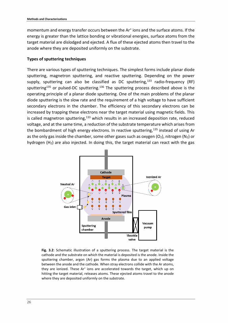
Methods and Characterizations
26
momentum and energy transfer occurs between the Ar+ ions and the surface atoms. If the
energy is greater than the lattice bonding or vibrational energies, surface atoms from the
target material are dislodged and ejected. A flux of these ejected atoms then travel to the
anode where they are deposited uniformly on the substrate.
Types of sputtering techniques
There are various types of sputtering techniques. The simplest forms include planar diode
sputtering, magnetron sputtering, and reactive sputtering. Depending on the power
supply, sputtering can also be classified as DC sputtering,133 radio-frequency (RF)
sputtering135 or pulsed-DC sputtering.136 The sputtering process described above is the
operating principle of a planar diode sputtering. One of the main problems of the planar
diode sputtering is the slow rate and the requirement of a high voltage to have sufficient
secondary electrons in the chamber. The efficiency of this secondary electrons can be
increased by trapping these electrons near the target material using magnetic fields. This
is called magnetron sputtering,133 which results in an increased deposition rate, reduced
voltage, and at the same time, a reduction of the substrate temperature which arises from
the bombardment of high energy electrons. In reactive sputtering,135 instead of using Ar
as the only gas inside the chamber, some other gases such as oxygen (O2), nitrogen (N2) or
hydrogen (H2) are also injected. In doing this, the target material can react with the gas
Fig. 3.2: Schematic illustration of a sputtering process. The target material is the cathode and the substrate on which the material is deposited is the anode. Inside the sputtering chamber, argon (Ar) gas forms the plasma due to an applied voltage between the anode and the cathode. When stray electrons collide with the Ar atoms, they are ionized. These Ar+ ions are accelerated towards the target, which up on hitting the target material, releases atoms. These ejected atoms travel to the anode where they are deposited uniformly on the substrate.

Methods and Characterizations
27
molecules to form a compound. For instance, in the case of reactive sputtering of silicon
in the presence of O2, SiO2 can be deposited on a substrate.
While a DC power supply is shown in Fig. 3.2 for sputtering, an alternating power supply
may be used instead. This is crucial for sputtering of insulating materials as charges can
build up if a constant DC supply is applied over time in a DC sputtering. This may lead to
arcing that can damage the target and a poor quality in the deposited film. Therefore, an
RF is commonly employed to deposit non-conducting materials. However, this comes at
the cost of reduced deposition rate and a high voltage compared to DC sputtering. Another
method to deposit insulating materials at a high rate is to use pulsed-DC sputtering. In this
method, the arcing is avoided for insulating materials without affecting the deposition
rate. Here, a reverse bias is applied for a very short period of time (typically in the order of
hundreds of µs) to discharge the accumulated charges.
3.1.3 Fabrication of a typical perovskite solar cell
In this thesis, the PSCs are fabricated in n-i-p architecture. Fig. 3.3 shows a schematic of
the fabrication of standard n-i-p architecture prepared in this group. The fabrication of
PSCs in this architecture comprises of the deposition of the electron transport layer (ETL)
on a transparent conductive oxide electrode followed by the deposition of the perovskite
active layer, hole transport layer (HTL) and the rear electrode. Various deposition
techniques are employed to realize each layer. The transparent conductive oxide
electrodes are obtained by sputtering the target material. The ETLs are deposited with
various deposition methods: spin coating, blade coating, inkjet printing and slot-die
coating. The perovskite absorber layers and the HTLs are obtained by spin coating method,
although inkjet printing and evaporation of the both the layers are feasible in this research
group.108,137 The buffer layers, anti-reflection coatings and the opaque electrodes are
obtained using thermal evaporation. In the case of semitransparent perovskite solar cells
(s-PSCs), gold fingers are deposited to increase the conductivity of the rear TCO. The
discussions below describe the fabrication of each of these layers in detail.
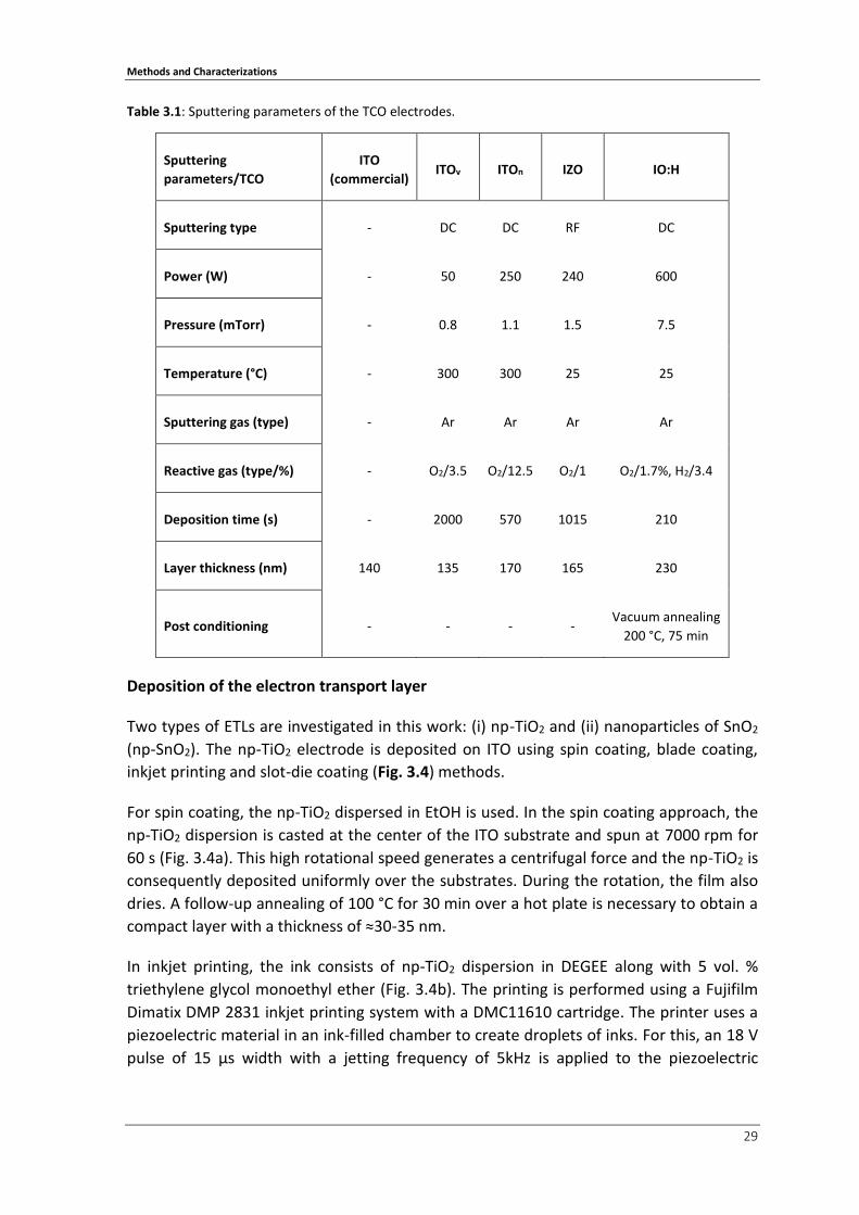
Sputtering of front transparent conductive oxide electrode
Typically, tin-doped indium oxide (ITO) is used as the TCO electrode, either purchased
commercially (Luminescence Technology) or sputtered in-house. Two types of ITO
electrodes are sputtered in-house: ITOv and ITOn. ITOv is used as the TCO for the devices in
chapter 6, section 6.1, while ITOn is used as the TCO in chapter 6, section 6.2. Zinc-doped
indium oxide (IZO) is also sputtered in-house as the front TCO electrode in the PSC.
Hydrogen-dope indium oxide (IO:H) is obtained from the collaboration partner, ZSW. The
deposition parameters are given is Table 3.1.

Methods and Characterizations
28
Fig. 3.3: Schematic illustration of the fabrication of opaque and semitransparent perovskite solar cells in n-i-p architecture. The layer stack is comprised of TCO/ETL/Perovskite/HTL/TCO or metal back contact. The involved processes are sputtering and subsequent photolithography of TCOs, spin coating/inkjet printing/slot-die/blade coating of ETL, spin coating of perovskite absorber and HTL, thermal evaporation of buffer layer, anti-reflection coatings, rear electrodes or sputtering of rear TCO. Here, TCO, ETL and HTL stands for transparent conductive oxide, electron transport layer and hole transport layer, respectively.
Methods and Characterizations
29
Table 3.1: Sputtering parameters of the TCO electrodes.
Sputtering
parameters/TCO
ITO
(commercial) ITOv ITOn IZO IO:H
Sputtering type - DC DC RF DC
Power (W) - 50 250 240 600
Pressure (mTorr) - 0.8 1.1 1.5 7.5
Temperature (°C) - 300 300 25 25
Sputtering gas (type) - Ar Ar Ar Ar
Reactive gas (type/%) - O2/3.5 O2/12.5 O2/1 O2/1.7%, H2/3.4
Deposition time (s) - 2000 570 1015 210
Layer thickness (nm) 140 135 170 165 230
Post conditioning - - - - Vacuum annealing
200 °C, 75 min
Deposition of the electron transport layer
Two types of ETLs are investigated in this work: (i) np-TiO2 and (ii) nanoparticles of SnO2
(np-SnO2). The np-TiO2 electrode is deposited on ITO using spin coating, blade coating,
inkjet printing and slot-die coating (Fig. 3.4) methods.
For spin coating, the np-TiO2 dispersed in EtOH is used. In the spin coating approach, the
np-TiO2 dispersion is casted at the center of the ITO substrate and spun at 7000 rpm for
60 s (Fig. 3.4a). This high rotational speed generates a centrifugal force and the np-TiO2 is
consequently deposited uniformly over the substrates. During the rotation, the film also
dries. A follow-up annealing of 100 °C for 30 min over a hot plate is necessary to obtain a
compact layer with a thickness of ≈30-35 nm.
In inkjet printing, the ink consists of np-TiO2 dispersion in DEGEE along with 5 vol. %
triethylene glycol monoethyl ether (Fig. 3.4b). The printing is performed using a Fujifilm
Dimatix DMP 2831 inkjet printing system with a DMC11610 cartridge. The printer uses a
piezoelectric material in an ink-filled chamber to create droplets of inks. For this, an 18 V
pulse of 15 μs width with a jetting frequency of 5kHz is applied to the piezoelectric

Methods and Characterizations
30
material. This changes the shape of the piezoelectric material and creates a pressure in the
fluid and consequently, a droplet of ink is ejected from the nozzle. During printing, 10 pL
of the ink is used and both the ink and the substrate plate are held at controlled
temperatures of 35 °C and 22 °C. A drop spacing of 35 μm and subsequent drying in vacuum
for 2 min, before annealing at 100 °C leads to a compact film of ≈35 nm.
The np-TiO2 is also deposited with blade coating technique (Fig. 3.4c) using the dispersion
in EtOH. For this, a Zehntner ZAA 2300 system blade coater is used. The system uses a
running blade with a variable speed setting. A diluted np-TiO2 dispersion in EtOH (1:2.5) is
dropped on the samples and the blade is moved over the substrate at a speed of 6 mm/s.
After an annealing step at 100 °C for 30 min, a 30-35 nm thick layer is obtained.
For slot-die coating of np-TiO2, the dispersion in 1-butanol is used (Fig. 3.4d). After diluting
to 50 vol %, slot-die coating is performed with an nTact Coating System nRad in a controlled
cleanroom condition, at a temperature of 23 °C with a relative humidity of 50%. In slot-die
coating, the layer is obtained by the flow of the ink through a slot-die head on a moving
substrate. A 6-8 μm thick wet layer is obtained to ensure a final dry layer of ≈35 nm. The
drying is performed by keeping the samples for 2 min at the room temperature, followed
by 1 min at 55 °C, and finally annealing at a temperature of 100 °C.
For the np-SnO2 ETL, a colloidal dispersion of np-SnO2 (Alfa Aesar) of ≈15 wt% is used. The
dispersion is diluted to 2.04 wt% in de-ionized water and spin-coated at a speed of 4000
rpm for 30 s. A follow-up annealing step of either 150 °C or 250 °C for 30 min is used to
obtain the ETL with a thickness of ≈10 nm.
Deposition of the perovskite absorber
Three different perovskite absorbers are used for the fabrication of PSCs in this thesis: (i)
MAPI (CH3NH3PbI3), (ii) triple cation (Cs0.1(MA0.17FA0.83)0.9Pb(I0.83Br0.17)3), and (iii) double
cation (FA0.83Cs0.17Pb(I1−yBry)3), where 0.24≤y≤0.56. The following precursors are used:
(i) Methylammonium iodide, MAI (Greatcell solar)
(ii) Formamidinium iodide, FAI (Greatcell solar)
(iii) Methylammonium bromide, MABr (Greatcell solar)
(iv) n-butyl ammonium bromide, n-BABr, (Greatcell solar)
Fig. 3.4: Schematic illustration of the deposition of np-TiO2 using various deposition
technique: spin coating, inkjet printing, blade and slot-die coating. Reproduced with
permission from ACS Applied Energy Materials, [139] © American Chemical Society.
Methods and Characterizations
31
(v) Cesium iodide, CsI (Alfa Aesar)
(vi) Lead iodide, PbI2 (TCI or Alfa Aesar)
(vii) Lead bromide, PbBr2 (TCI or Alfa Aesar)
(viii) Lead chloride, PbCl2 (Merck)
(ix) Lead acetate trihydrate, Pb(CH3CO2)2·3H2O (Merck)
(x) N,N-dimethylformamide, DMF (Merck)
(xi) Dimethyl sulfoxide, DMSO (Merck)
(xii) γ-butyrolactone, GBL (Merck)
(xiii) Isopropanol, IPA (Merck)
(xiv) Chlorobenzene, CB (Merck)
MAPI is deposited in two different methods. The first method consists of solution of
CH3NH3PbI3 prepared from the precursors of MAI, PbCl2, Pb(CH3CO2)2·3H2O. For this, two
separate solutions are prepared: (i) Pb(CH3CO2)2·3H2O and MAI are dissolved in DMF in a
ratio of 1:3, and (ii) PbCl2 and MAI dissolved in DMF in a ratio of 1:3. Solution 2 is then
mixed with solution 1 to obtain ≈20% PbCl2 in the final solution. Spin coating is performed
at 3000 rpm for 30 s and annealing at 115 °C for 10 min inside a glovebox environment (0.1
ppm O2 and 0.1 ppm H2O) forms the ≈300−350 nm thick CH3NH3PbI3 layer. The second
method consists of an anti-solvent approach and is only used to deposit the perovskite
absorber on slot-die coated np-TiO2. The CH3NH3PbI3 solution is prepared from a mixture
of PbI2 and MAI (ratio 1:1) dissolved in GBL, DMSO, and DMF in a ratio of 1:1:1. The spin
coating is performed in two separate steps inside the glovebox (0.1 ppm O2 and 0.1 ppm
H2O): (i) 1000 rpm for 15 s, and (ii) 4000 rpm for 45 s. Toluene is released 25 s before the
end of the second step. The samples are annealed at 100 °C for 10 min to obtain a final
layer of thickness ≈335−340 nm.
Triple cation perovskite is prepared from the precursors of MABr, FAI, PbI2 PbBr2 and CsI.
For this, two separate solutions are prepared: (i) a precursor solution of FAI (1 M), PbI2
(1.1 M), MABr (0.2 M), and PbBr2 (0.2 M) in DMF:DMSO in a ratio of 4:1, and (ii) a stock
solution of CsI in DMSO (1.5 M). An 88.9 μL aliquot of solution 2 is transferred into solution
1 to prepare the final mixture. Two spin-coating steps are used to obtain the desired layer:
(i) 1000 rpm for 10 s and (ii) 6000 rpm for 20 s. 100 µL CB is released 5-7 s before the end
of the second step and the samples are annealed at 100 °C for 1 h.
Double cation perovskite is prepared for both 3D and 2D/3D perovskite heterojunction
layers. For preparing the 3D perovskite absorber layers of five different bandgaps, the
amount of bromide content in the precursor solution is varied between 0.24 ≤ y ≤ 0.56 in
steps of Δy = 0.08. The perovskite precursor solution is prepared by dissolving 0.83 mmol
FAI, 0.17 mmol, ((2 – 3 × y))/2) mmol PbI2, and (3/2 × y) mmol PbBr2 in a 1 mL solvent
mixture of DMF and DMSO (4:1). Two spin-coating steps are used to obtain the desired
layer inside the glovebox (0.1 ppm O2 and 0.1 ppm H2O): (i) 1000 rpm for 10 s and (ii) 5000
rpm for 30 s. 100 µL CB is released 5−7 s before the end of the second step and the samples
are annealed at 100 °C for 1 h.
Methods and Characterizations
32
To obtain the 2D/3D perovskite heterostructure, 2 mg/mL of n-BABr in isopropanol is
prepared. 100 µL of n-BABr solution is spin-coated dynamically on 3D perovskite at 5000
rpm for 30 s with a subsequent annealing at 100 °C for 5 min inside the glovebox (0.1 ppm
O2 and 0.1 ppm H2O).
Spin coating of the hole transport layer
N,N′-di-p-methoxy phenylamine)-9,9′-spirobifluorene, spiro-OMeTAD (Luminescence
Technology) is deposited by spin-coating at 4000 rpm for 30 s. The precursor solution is
prepared from 80 mg of spiro-OMeTAD dissolved in 1 mL CB with the additives of 17.5 µL
lithium salt solution and 28.5 µL 4-tert butylpyridine (Sigma Aldrich). The lithium salt
solution is prepared by dissolving 520 mg lithium bis(trifluoromethanesulfonyl) imide
(Sigma Aldrich or Merck) in 1 mL of acetonitrile (Sigma Aldrich or Merck). After the
deposition, the samples are left for oxygen doping in ≈25% relative humidity condition for
≈12 h.
Thermal evaporation of the buffer layer, opaque electrode and the anti-reflection
coating
The 10 nm thick buffer layer of MoOX (Sigma Aldrich or Merck) deposited on the HTL and
the 165 nm anti-reflection coating of MgF2 (Sigma Aldrich or Merck) on the rear ITO are
thermally evaporated using Lesker Spectros PVD system or Angstrom Engineering at a rate
of ≈0.8 Å/s and 3-4 Å/s, respectively under a pressure of 6 x 10⁻⁶ mbar. The buffer layer
and the anti-reflection coating are deposited only for fabricating s-PSCs. For opaque
perovskite solar cells (o-PSCs) as shown in Fig. 3.2, a rear Au contact (60 nm or 75 nm) is
evaporated directly on the HTL using a Vactec Coat 320 evaporator system. The resultant
active area of the o-PSCs is 10.5 mm2.
Sputtering of rear transparent conductive oxide electrode
The s-PSCs are fabricated employing TCO electrodes on the rear side. For this, either an
ITO or an IZO layer is sputtered on the buffer MoOX layer (Fig. 3.2). In contrast to front TCO
electrodes, the rear TCO electrodes are sputtered at room temperature (25 °C). Along with
low temperature deposition, the power is lowered so that the heat developed due to the
bombardment on the substrate during sputtering is reduced. Since sputtering is not
directional, sharp edges are not obtained and the active layer is not clearly defined.
Therefore, shadow masks with defined area are used for characterizing these s-PSCs (see
section 3.2.1 for more details). After the deposition of the rear TCO electrodes, gold fingers
are deposited to increase the conductivity further. The sputtering parameters used to
deposit these rear TCOs can be found in Table 3.2.

Methods and Characterizations
33
Table 3.2: Sputtering parameters of the rear TCO electrodes.
Sputtering parameters/TCO ITO IZO
Sputtering type DC RF
Power (W) 50 100
Pressure (mTorr) 0.8 1.5
Temperature (°C) 25 25
Sputtering gas (type) Ar Ar
Reactive gas (type/%) O2/2.5 O2/1
Deposition time (s) 2310 2550
Post conditioning - -
Layer thickness (nm) 165 165
3.1.4 Fabrication of nanostructured ITO
NS ITO is fabricated to reduce reflection losses and improve light in-coupling. Two
configurations of NS ITO are fabricated: (i) periodic, and (ii) disordered. In the following
sections, the fabrication process of periodic and disordered NS ITO is discussed in detail.
Periodic nanostructured ITO
The periodic NS ITO is fabricated by employing soft-imprinting molds of nanostructures
and subsequent sputtering of ITO. Fig. 3.5a shows the schematic to obtain the periodic NS
ITO. To fabricate periodic NS ITOs, first a master structure is fabricated on silicon wafer
using electron beam lithography for periods p = 200 nm, 300 nm, 400 nm and 500 nm. The
geometrical filling fraction of the master structure, which is defined by the ratio of the
nanostructured area to the total area:
𝐹𝑖𝑙𝑙𝑖𝑛𝑔 𝐹𝑟𝑎𝑐𝑡𝑖𝑜𝑛 =
𝜋𝑑2
4𝑝2
(3.1)
is set to 0.35 with a depth of 100 nm. These parameters are close to the optimum and is
obtained from simulation study carried out by Goth.138 The master structure is then
replicated on a bilayer mold of hard polydimethylsiloxane (hPDMS) and PDMS. A mixture
of hPDMS with a cross-linker in a ratio of 1:1 (outgassed for 30 min in a desiccator) is spin
coated on the master structure at a speed of 5000 rpm for 30 s, followed by an annealing

Methods and Characterizations
34
of 10 min at 60 °C. Next, the PDMS is mixed with a curing agent (in ratio 10:1 and outgassed
for 30 min in a desiccator) is drop-casted on the sample and heated at 60 °C for 1 h,
followed by 100 °C for another 1 h. The mold is then carefully removed from the silicon
wafer.
To obtain the nanopillars, a commercial polymer named OrmoComp is drop-casted on the
nanostructure mold and pressed with a glass substrate under a small weight (300 mg). This
stack is left on the hotplate for 5 min at 60 °C. The stack is then UV exposed for 5 min to
cure the resist and followed by carefully removing the nanostructured glass superstrate
from the stamp. The obtained samples are then heated at 130 °C for another 30 min.
Finally, ITO is sputtered on the nanostructures to obtain the NS ITO. The sputtering
conditions are as follows: power = 50 W, pressure = 0.8 mTorr, temperature = 25 °C,
sputtering gas = Ar with 2.5% O2 as the reactive gas, deposition time = 2000 s. A subsequent
post annealing at 200 °C for 15 min improves both the transmission and conductivity of
the final NS ITO. The planar ITO, which is the reference TCO, is fabricated by sputtering ITO
directly on glass in the same sputtering run.
Fig. 3.5: (a) Schematic illustration of the fabrication of periodic nanopillars. First a mold of hPDMS and PDMS with predefined nanostructured dimensions is prepared. Next critical step involves application of OrmoComp on this mold and pressing with a glass substrate, followed by heating and annealing steps. Finally, sputtering of ITO leads to the formation of NS ITO. (b) Picture of a period nanostructured ITO demonstrating diffraction of light. Adapted from reference [138].

Methods and Characterizations
35
Disordered nanostructured ITO
Polymer blend lithography is employed to fabricate disordered NS ITO. Fig. 3.6 shows the
schematics to obtain disordered NS ITO. A blend of polystyrene, PS (molecular weight:
3.25k, Sigma Aldrich) and poly(methyl methacrylate), PMMA (molecular weight: 5.50k,
Sigma Aldrich) dissolved in methyl ethyl ketone, MEK (Sigma Aldrich) in a mass ratio of 4/6,
15 mg/ml is used. The solution is placed on a hot plate at 100 °C for an hour to dissolve the
solution. A 40 µl aliquot of the solution is spin coated onto the glass substrate at a speed
of 3000 rpm for 30 s at a humidity ≈45%). The samples are then exposed to O2 plasma for
30 s at a power of 50 W. Finally, the PS nanopillars are obtained by developing the samples
in acetic acid (concentration of 99%, Alfa Aesar) that removed the PMMA. The ITO is
sputtered on the nanopillars of PS in the same manner as described previously for periodic
NS ITO.
3.2 Characterization Techniques
To evaluate the performance of the fabricated PSCs, the devices and layers are
characterized electrically and optically with various tools. Details regarding each tool are
described in the following section.
Fig. 3.6: Schematic illustration of the fabrication of disordered nanostructured ITO (NS ITO). PS and PMMA stands for polystyrene and poly(methyl methacrylate), respectively. A blend of PS and PMMA is first spin coated on a glass substrate. After selective development of PMMA, PS nanopillars are obtained. Finally, sputtering of ITO leads to the formation of NS ITO. Adapted with permission from reference [71], © 2020 Optical Society of America.

Methods and Characterizations
36
3.2.1 Electrical characterization
Current density-voltage (J-V) characteristics
The performance of the fabricated PSCs is determined by a solar simulator. Typical current
density-voltage (J-V) characteristic of a solar cell is shown in Fig. 2.4. The J-V characteristics
of the investigated PSCs are measured using a class AAA Newport solar simulator (xenon
lamp). The measurements are performed under standard test conditions. This means that
the PSCs are illuminated at 1000 W/m2 with a continuous illumination of AM 1.5G, keeping
the devices at 25 °C. The voltage is swept from open-circuit voltage (VOC) condition to
short-circuit current density (JSC) and vice-versa using a Keithley 2400 source meter. This
allows the determination of hysteresis in PSCs. A constant sweeping rate of 600 mV/s is
used. The temperature of the samples is actively controlled using a self-made Peltier
element control circuit. For the o-PSCs, the devices are measured without any shadow
masks as the active area is clearly defined by the overlap between the ITO and gold layouts.
For s-PSCs, shadow mask of 5.6 mm2 is employed to define an aperture area for the
devices.
The c-Si solar cell or CIGS solar cell is measured either stand-alone or under the filters of
s-PSCs prepared during the fabrication of the solar cells. A filter consists of the same layer
stack as the s-PSCs and have optical properties as that of the s-PSCs but with a larger area
(16 mm x 16 mm). The schematic of a tandem measurement setup is illustrated in Fig. 3.7.
An air gap exists between the sub-cells as no additional material is used as a spacer
Fig. 3.7: Schematic illustration of a tandem solar cell measurement setup. The bottom crystalline-silicon (c-Si) or CIGS solar cells are measured through a filter of a top perovskite solar cell. A filter consists of the same layer stack as the s-PSCs and have optical properties as that of the s-PSCs but with a larger area. An aperture area is defined with the shadow masks to measure the bottom solar cells. Adapted with permission from reference [99], © John Wiley & Sons.

Methods and Characterizations
37
between the top s-PSC filters and the bottom solar cells. A shadow mask with an aperture
area of 72 mm2 or 165 mm2 is used to define the active area. The final power conversion
efficiency (PCE) of the 4T tandem configuration is obtained by the sum of the top s-PSC
PCE and the bottom c-Si or CIGS solar cell PCE.
External quantum efficiency
As discussed in section 2.1 Chapter 2, external quantum efficiency (EQE), measurements
are performed to determine the spectral response of the PSCs. The measurements are
carried out using a Bentham PVE300 system. In contrast to the solar simulator, light is
incident on the sample with a much lower intensity that results in a reduction of signal-to-
noise ratio. Therefore, the EQE system uses a lock-in amplifier technique with a reference
signal having a chopping frequency of ≈930 Hz, which reliably improves the signal-to-noise
ratio. Integration times of 500 ms are used to obtain the signal.
Four-point probe technique
Four-point probe measurements are performed to measure the sheet resistance of the
TCOs. The schematic of a typical four-point probe setup is illustrated in Fig. 3.8. The outer
pins 1 and 4 are used to drive a current through the film. This generates a voltage across
the resistance of the film. The inner pins 2 and 3 measure the generated voltage. Since,
there is no current flowing though pins 2 and 3, the voltage drop across these contacts is
neglected. Here, a custom made four-point setup is used to measure sheet resistances of
various TCOs. The setup includes an S-302 four-point probe mounting stand and a Picotest
M3500A multi-meter. The sheet resistance can be calculated by:
𝑅𝑠ℎ =
𝜋
ln (2)
∆𝑉
𝐼
(3.2)
Fig. 3.8: Schematic illustration of a four-point probe setup for measuring sheet
resistance of transparent conductive oxide (TCO) electrodes.
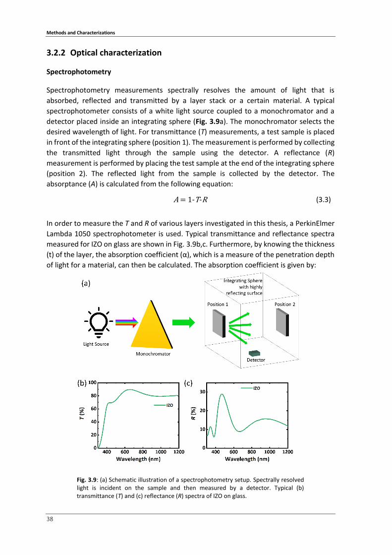
Methods and Characterizations
38
3.2.2 Optical characterization
Spectrophotometry
Spectrophotometry measurements spectrally resolves the amount of light that is
absorbed, reflected and transmitted by a layer stack or a certain material. A typical
spectrophotometer consists of a white light source coupled to a monochromator and a
detector placed inside an integrating sphere (Fig. 3.9a). The monochromator selects the
desired wavelength of light. For transmittance (T) measurements, a test sample is placed
in front of the integrating sphere (position 1). The measurement is performed by collecting
the transmitted light through the sample using the detector. A reflectance (R)
measurement is performed by placing the test sample at the end of the integrating sphere
(position 2). The reflected light from the sample is collected by the detector. The
absorptance (A) is calculated from the following equation:
A = 1-T-R (3.3)
In order to measure the T and R of various layers investigated in this thesis, a PerkinElmer
Lambda 1050 spectrophotometer is used. Typical transmittance and reflectance spectra
measured for IZO on glass are shown in Fig. 3.9b,c. Furthermore, by knowing the thickness
(t) of the layer, the absorption coefficient (α), which is a measure of the penetration depth
of light for a material, can then be calculated. The absorption coefficient is given by:
Fig. 3.9: (a) Schematic illustration of a spectrophotometry setup. Spectrally resolved light is incident on the sample and then measured by a detector. Typical (b) transmittance (T) and (c) reflectance (R) spectra of IZO on glass.

Methods and Characterizations
39
α =
1
tln
(1-R)2
T
(3.4)
Ellipsometry
Ellipsometry is a non-invasive technique for measuring the dielectric properties of thin
films. It measures the change in polarization when an incident light of known polarization
is reflected from the thin film surface (Fig. 3.10a). The change in the polarization is related
to the Fresnel reflection coefficients, rs and rp and is represented by:
ρ = rs
rp= tan ψ . 𝑒𝑖𝛥 (3.5)
where, ρ is the complex reflectance ratio, tan ψ is the amplitude ratio upon reflection, and
Δ is the phase shift. By using an accurate model derived from electromagnetic theory, such
as Lorentz model and Drude model, the complex refractive index of the materials can be
evaluated. In this thesis, the refractive indices and extinction coefficients of TCOs and
charge transport layers are determined using a Woolam Variable Angle Spectroscopic
Elliosometry (WVASE). Refractive index and extinction coefficient of commercial ITO can
Fig. 3.10: (a) Schematic illustration of an ellipsometry setup. The change in the
polarization of light is used to determine the film or sample properties. (b) Refractive
index (n) and (c) extinction coefficient (k) of tin-dope indium oxide (ITO) electrode
derived from ellipsometry.

Methods and Characterizations
40
be found in Fig. 3.10b,c. The analysis is performed with the software provided by the
manufacturer.
Photoluminescence spectroscopy
Photoluminescence spectroscopy is used to obtain insights about the electronic structure
and properties of a material. In this process, an incident light of energy above the bandgap
of the material is directed towards a sample, causing an electron to be excited in the
conduction band. After thermal relaxation, the exited electron recombines with a hole by
emitting photons (Fig. 3.11a,b). The emitted light is then spectrally resolved by a
monochromator and finally detected by a camera. Two types of photoluminescence
measurements are performed in this thesis: (i) steady-state photoluminescence
spectroscopy (SSPL), and (ii) time-resolved photoluminescence spectroscopy (TRPL). SSPL
spectroscopy investigates the long-term (several micro seconds to milli seconds) average
Fig. 3.11: (a) Absorption and (b) radiative recombination processes occurring during a photoluminescence spectroscopy measurement. Photons of energy higher than the bandgap of the material excites an electron from the valence band (VB) to the conduction band (CB). An excited electron in the CB can find a hole in the valance band and relax by emitting a photon. (c) Schematic illustration of a photoluminescence spectroscopy setup. A sample is excited by laser pulses. The excited electrons emit photons which are spectrally resolved by a monochromator and detected by a sensitive camera.

Methods and Characterizations
41
emission from a sample when exited by light. Various properties can be evaluated from
such a measurement, for instance, the determination of the bandgap, carrier distribution,
phonon scattering or structural homogeneity of the investigated material. TRPL
spectroscopy investigates the temporal evolution of the emission from a sample. In such a
measurement, the detection window is reduced to several pico seconds in contrast to
SSPL. This method can be used to determine the lifetime of charge carriers. In principle, a
longer lifetime of the charge carriers is preferred for the absorber materials as it indicates
reduced non-radiative recombination losses. Here, SSPL and TRPL measurements are
performed for perovskite absorbers or semitransparent PSCs with a custom-made setup.
A schematic of the typical photoluminescence spectroscopy setup is illustrated in Fig.
3.11c. A pulsed laser of 532 nm with a repetition rate of 1 kHz or 5 kHz is used to excite the
samples. The emission is detected using a CCD camera, PIMAX512 fed by an ACTON
spectrometer. For TRPL, a gated mode with a gate opening time of 3 ns is used. The
measurements are performed in air.
3.2.3 Material characterization
X-ray diffractometry
To investigate the crystallinity of a material, X-ray diffractometry (XRD) is performed. Every
crystalline material has a clear signature due to its unique crystal structure as the atoms
are arranged in a regular order. When these atoms are excited with electromagnetic wave
of wavelengths in the same order as the lattice dimension, they scatter light (Fig. 3.12).
The scattered or also referred as reflected wave can interfere constructively if the
following condition is satisfied:
2dsinθ = nλ; n = 1, 2, 3…. (3.6)
Fig. 3.12: (a) X-ray diffraction (XRD): Bragg’s law. (b) Typical XRD pattern of a perovskite crystal structure.

Methods and Characterizations
42
where, d is the distance between the planes, θ is the incident angle of the electromagnetic
wave, λ is the excitation wavelength and n is a constant. This is known as Bragg’s law of
diffraction. Each reflection from the planes inside the crystal lattice can be represented by
Miller indices. A typical XRD diffraction pattern for a perovskite film is shown in Fig. 3.12b.
In addition to the crystallinity, the crystallite size as well as strains induced in the crystal
structure can be determined via XRD measurements. In this thesis, XRD measurements are
performed to determine the crystal structure of np-TiO2, perovskite absorbers and TCOs.
The measurements are carried out using a Bruker D2 phaser XRD system with a Cu Kα
radiation source. Typical excitation powers are 30 keV.
X-ray photoelectron spectroscopy
To obtain an insight about the chemical composition of a certain material, x-ray
photoelectron spectroscopy (XPS) is performed. In this technique, x-rays are irradiated on
a material in ultra-high vacuum due to which electrons are emitted from the atomic
orbitals for the first few nanometers of the material’s surface. An electron detector and
electron energy analyzer provide the number of electrons that are emitted and their
respective kinetic energy (Ek), which are then used to deduce the binding energy (EB) of
respective electrons (Equation 3.7). The obtained binding energy is associated to the
respective orbital from which the electron is emitted and depends both on the element
and its chemical environment. The work function (φ) is the minimum energy required to
eject an electron from the material outside its surface.
hν = 𝐸𝑘+𝐸𝐵+ϕ (3.7)
Here, XPS measurements are performed on np-TiO2 using a Kα+ XPS spectrometer from
Thermo Fisher Scientific. The samples are analyzed using a micro-focused,
monochromated Al Kα X-ray source with a spot size of 400 μm. The spectra are fitted with
one or more Voigt profiles, and referenced to C 1s peak of hydrocarbon at 285.0 eV binding
energy.
Scanning electron microscopy
Since the dimension of the investigated layers are in the order of few tens to hundreds of
nanometers, ordinary optical microscope cannot resolve these layers. Thus, a scanning
electron microscope (SEM) is used to visualize them. In a SEM setup, beams of electrons
produced with an electron gun that are accelerated by a large potential (tens of kilo volts)
inside a vacuum chamber. The path of the beam is controlled with some deflection coils
before focusing them on the sample using condensing lenses. Up on interaction with a
sample, the electrons are either backscattered or secondary electrons are created. In some
cases, x-rays are also emitted. All these signals are detected using very sophisticated
detectors to produce a final image of the sample. Here, the SEM images are obtained for
investigating perovskite absorber layers, charge transport layers and TCOs. The
measurement is performed using a Leo 1530 (Zeiss) SEM with both in-lens and secondary

Methods and Characterizations
43
detectors. Typical accelerating voltages of 5−10 keV with aperture of 30 μm are used to
obtain the images.
Atomic force microscopy
The surface roughness of a layer is determined using atomic force microscopy (AFM). This
measurement provides information about the topography of the sample surface with a
high resolution in orders of a few nanometers. The AFM system comprises of a cantilever,
an X-Y stage, a Z-scanner and a position scanner (Fig. 3.13a). A laser beam, which is
directed towards the cantilever, is reflected onto the position scanner. The X-Y stage is
used to move around the sample surface and if there is a change in the surface topography,
the position of the Z-scanner is altered. Thus, an image of the surface morphology is
obtained. A non-contact or tapping method is used to obtain the surface morphology of
the investigated samples, which helps in retaining the tip sharpness and leaves the surface
unharmed. In this thesis, AFM is performed to determine the morphology of NS ITO and
surface roughness of various TCOs. An AFM image of a periodic NS ITO is shown in
Fig. 3.13b. The samples are investigated in ambient conditions with an AFM system from
dimension icon, Veeco with a NanoScope V controller. Typical scan sizes are 5 µm x 5 µm
or 10 µm x 10 µm with resolutions of up to 512 x 512 pixels.
Fig. 3.13: (a) Schematic illustration of an atomic force microscopy setup. (b) Atomic force microscopy (AFM) image of periodic nanostructured ITO.

Methods and Characterizations
44
45
4. Nanoparticle-based electron transport layers for
semitransparent perovskite solar cells
This chapter deals with research question 1 and discusses nanoparticle-based electron
transport layers (ETLs) for perovskite solar cells (PSCs). It includes a detailed study of the
various material properties of said nanoparticles. Two types of nanoparticle-based ETLs
are investigated: (i) nanoparticles of titanium dioxide (np-TiO2), and (ii) nanoparticles of tin
oxide (np-SnO2). An in-house synthesis is employed to prepare the np-TiO2. Furthermore,
in-depth studies regarding various synthesis parameters and some compelling features of
the np-TiO2 are described. The np-SnO2, extensively used as an alternative ETL in this
thesis, is purchased from a commercial manufacturer. The chapter concludes with a
comparative study of the optical properties and the photovoltaic characteristics of the
PSCs fabricated with these ETLs.
Acknowledgments and contributions
The major part of this chapter on the nanoparticle-based electron transport layer for
perovskite solar cells was already published in reference [139]. The publication of the
research article was a collaboration between KIT, IMEC and Solliance. In this collaboration,
Ihteaz M. Hossain conducted and analyzed most of the synthesis of np-TiO2, material
characterization (optical), and fabrication of perovskite solar cells. Ihteaz M. Hossain
acknowledges the support of Adrian Mertens in the analysis of the optical constants and
the support of Jonas Alexander Schwenzer, who performed the initial studies of the
development of np-SnO2 ETL in this research group.
Nanoparticle-based electron transport layers for semitransparent perovskite solar cells
46
The significant advancement in the field of perovskite photovoltaics is a result of a better
comprehension of the crystallization dynamics of the absorber layer,140 the compositions
of the absorber material,32,34 the passivation of defects,91 a superior electron- and hole-
transport layers (ETLs and HTLs) with improved charge selectivity,70,80 and well-aligned
energy levels with the absorber.141 In terms of ETL, a lot of materials were previously
investigated to fulfill the following criteria: (1) wide-bandgap of the ETL to avoid any
parasitic losses, (2) well-aligned energy level to the highest occupied molecular orbital of
the perovskite absorber layer to ensure a barrier-free transfer of electrons to the
respective ETL and reduce energy losses, and (3) a fast extraction of electrons to the
respective contact. Therefore, several ETLs including TiO2,48 SnO2,142 ZnO,142 WO3,142 and
organic fullerenes143 were studied in literature regarding the above criteria.
The most widely used ETL is TiO2 with which some of the highest power conversion
efficiencies (PCEs) of the perovskite solar cells (PSCs) are reported.31–34 TiO2 possesses fast
charge extraction of charges with mobilities of 0.1-10 cm2/V s.144 To achieve high PCEs, the
TiO2 ETL is deposited in a sequence of a compact layer followed by a mesoporous structure.
The compact TiO2 acts as a blocking layer,145 thus preventing holes from reaching the
transparent conductive oxide (TCO) in a n-i-p architecture. The mesoporous layer acts as
scaffold for the perovskite absorber.146 One important aspect to consider here is the
deposition of the TiO2 transport layer. The deposition of high-quality TiO2 ETL for efficient
PSCs involves solution processing of the precursor material and a post-annealing of
> 450 °C to ensure the crystalline anatase phase of TiO2.35,147 This crystalline phase ensures
high mobility in TiO2 ETL. The annealing step is very high in energy demand and
incompatible with conventional TCO electrodes such as indium-doped tin oxide (ITO) or
low-cost flexible plastic substrates. As a consequence, this process is not adequate for
upscaling techniques that involve roll-to-roll fabrication of PSCs. Moreover, fluorine-doped
tin oxide (FTO) substrates must be employed to fabricate PSCs. FTO electrodes are
compatible with high-temperature annealing processes, but are not suitable for efficient
perovskite/c-Si or perovskite/CIGS tandem solar cells due to their high near-infrared (NIR)
parasitic absorption (also see Appendix, Fig. A. 4.1).36 Both of these factors motivate the
research to alternative approaches to process the TiO2 or investigation of different
materials as ETLs.
In order to overcome the limitation of high temperature processing of TiO2, an alternative
approach is described in this study as the first strategy with the promise of up-scalable and
highly transparent semitransparent perovskite solar cells (s-PSCs) for tandem architecture.
This includes pre-synthesis of in-house nanoparticles of titanium-dioxide (np-TiO2) in its
crystalline anatase phase and the subsequent deposition of the np-TiO2 on a substrate as
the ETL at a lower temperature, which is compatible with ITO or flexible substrates. The
material properties as well as the photovoltaic performance of the fabricated PSCs on the
various synthesis parameters are investigated in detail including the effect of doping,
synthesis time and solvent systems.
As a second strategy, commercially available nanoparticle of tin-oxide (np-SnO2) is also
investigated for PSCs. In recent studies, focus is placed on SnO2 ETL due to following

Nanoparticle-based electron transport layers for semitransparent perovskite solar cells
47
reasons: (i) bulk mobility of SnO2 is significantly higher than TiO2 (100 times),148 (ii) SnO2 is
a wide-bandgap material,70 resulting in less parasitic absorption, and (iii) SnO2 has a deep
conduction band,148 indicating a better electron extraction from the absorber and ensuring
improved hole blocking. Moreover, it is reported that SnO2 exhibits excellent chemical
stability in comparison to TiO289 and can be deposited at low temperatures, ensuring the
feasibility of roll-to-roll processing and compatibility with highly transparent ITO
electrodes.142 In order to compare and find the optimum ETL for the application in
perovskite-based tandems, a comparative study based on the photovoltaic performance
and stability of the PSCs with these two ETLs are discussed at the end of this chapter.
4.1 np-TiO2 ETL for perovskite solar cells The overall performance of the fabricated PSCs depends highly on the material properties
of the ETL. Therefore, in this section, the crystallinity and the bandgap of the synthesized
np-TiO2 are investigated. Moreover, since the np-TiO2 are prepared in-house, several
processing parameters (size, solvent system and doping) are investigated, which allows
additional degrees of freedom to obtain np-TiO2 with compelling features.
4.1.1 Material properties of np-TiO2
The synthesis process described in the chapter 3, section 3.1 results in the formation of
crystalline np-TiO2. In order to investigate the crystal structure and the type of polymorph,
X-ray powder diffraction (XRD) measurements are carried out with a Kα excitation obtained
from a Cu source. The nanoparticles are drop-casted from the dispersion on a silicon
substrate and allowed to dry before being investigated. A strong reflection peak at
2θ ≈25.3° indicates the presence of the <101> plane of the crystal lattice (Fig. 4.1).
Furthermore, weak reflection peaks at 2θ ≈37.7°, 47.7°, and 54.0° represent the existence
of <004>, <200> and <105> planes, respectively. These results prove the crystalline nature
of the synthesized nanoparticles. In order to determine the phase of the np-TiO2, the
obtained XRD peaks are compared to the literature reflection peaks of the anatase and the
Fig. 4.1: X-ray diffraction (XRD) pattern of np-TiO2 (red) presented with the typical
positions of anatase TiO2 (green) and rutile TiO2 (orange) phase. The presence of the
typical reflection peaks from plane <004>, <200> and <105> and the absence of the
typical reflection peak at 2θ ≈27.4° of the rutile polymorph indicates that the np-TiO2
crystallize in its anatase phase. Reproduced with permission from ACS Applied Energy
Materials, [139] © American Chemical Society.
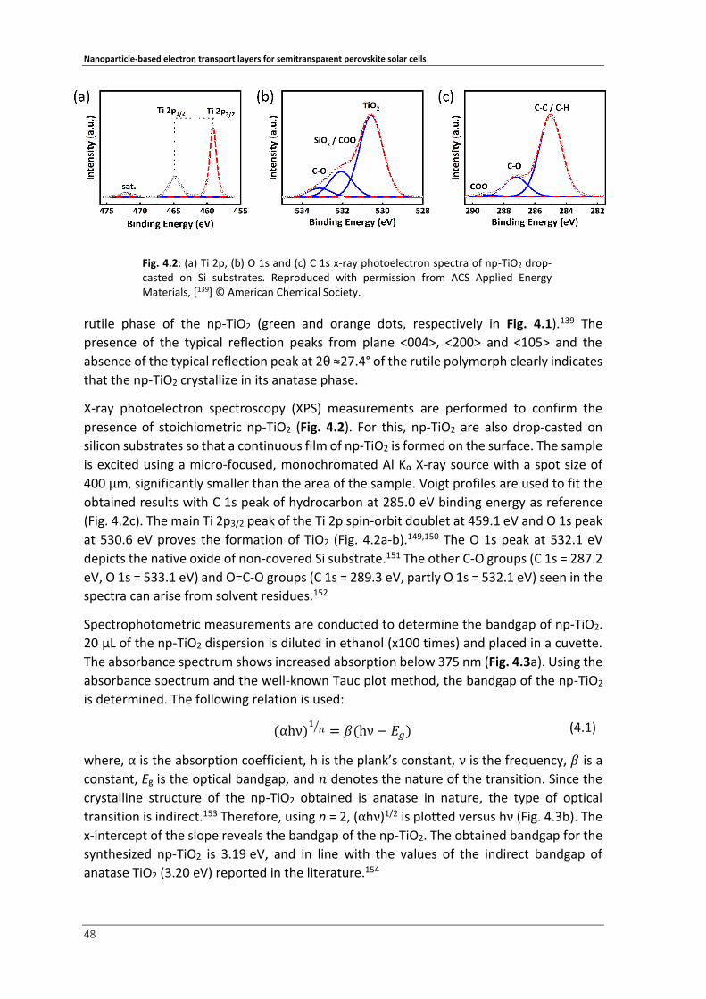
Nanoparticle-based electron transport layers for semitransparent perovskite solar cells
48
rutile phase of the np-TiO2 (green and orange dots, respectively in Fig. 4.1).139 The
presence of the typical reflection peaks from plane <004>, <200> and <105> and the
absence of the typical reflection peak at 2θ ≈27.4° of the rutile polymorph clearly indicates
that the np-TiO2 crystallize in its anatase phase.
X-ray photoelectron spectroscopy (XPS) measurements are performed to confirm the
presence of stoichiometric np-TiO2 (Fig. 4.2). For this, np-TiO2 are also drop-casted on
silicon substrates so that a continuous film of np-TiO2 is formed on the surface. The sample
is excited using a micro-focused, monochromated Al Kα X-ray source with a spot size of
400 μm, significantly smaller than the area of the sample. Voigt profiles are used to fit the
obtained results with C 1s peak of hydrocarbon at 285.0 eV binding energy as reference
(Fig. 4.2c). The main Ti 2p3/2 peak of the Ti 2p spin-orbit doublet at 459.1 eV and O 1s peak
at 530.6 eV proves the formation of TiO2 (Fig. 4.2a-b).149,150 The O 1s peak at 532.1 eV
depicts the native oxide of non-covered Si substrate.151 The other C-O groups (C 1s = 287.2
eV, O 1s = 533.1 eV) and O=C-O groups (C 1s = 289.3 eV, partly O 1s = 532.1 eV) seen in the
spectra can arise from solvent residues.152
Spectrophotometric measurements are conducted to determine the bandgap of np-TiO2.
20 μL of the np-TiO2 dispersion is diluted in ethanol (x100 times) and placed in a cuvette.
The absorbance spectrum shows increased absorption below 375 nm (Fig. 4.3a). Using the
absorbance spectrum and the well-known Tauc plot method, the bandgap of the np-TiO2
is determined. The following relation is used:
(αhν)1
𝑛⁄ = 𝛽(hν − 𝐸𝑔) (4.1)
where, α is the absorption coefficient, h is the plank’s constant, ν is the frequency, 𝛽 is a
constant, Eg is the optical bandgap, and 𝑛 denotes the nature of the transition. Since the
crystalline structure of the np-TiO2 obtained is anatase in nature, the type of optical
transition is indirect.153 Therefore, using n = 2, (αhν)1/2 is plotted versus hν (Fig. 4.3b). The
x-intercept of the slope reveals the bandgap of the np-TiO2. The obtained bandgap for the
synthesized np-TiO2 is 3.19 eV, and in line with the values of the indirect bandgap of
anatase TiO2 (3.20 eV) reported in the literature.154
Fig. 4.2: (a) Ti 2p, (b) O 1s and (c) C 1s x-ray photoelectron spectra of np-TiO2 drop-casted on Si substrates. Reproduced with permission from ACS Applied Energy Materials, [139] © American Chemical Society.

Nanoparticle-based electron transport layers for semitransparent perovskite solar cells
49
4.1.2 Additional features of np-TiO2
The synthesis procedure described chapter 3, section 3.1 forms stoichiometric np-TiO2 in
its crystalline anatase phase as concluded in the previous section. The in-house
preparation of the np-TiO2 also allows further possibility to tune the properties of
nanoparticles. In this regard, the influence of doping and variations of the synthesis
parameters such as time and solvent systems are investigated, which demonstrate some
more appealing features of the np-TiO2.
First, the doping of the np-TiO2 is investigated. Although previously it was reported that
np-TiO2 can be doped with yttrium,155 here, the np-TiO2 is doped with Nb5+ to improve the
conductivity of the ETL. During the first step of the synthesis as discussed on chapter 3,
section 3.1, NbCl5 (7 at. %) is included as additional material in the precursor solution. To
investigate the presence of Nb5+ ions, XPS measurements are performed, similar to the
procedure described earlier. The peak at 207.4 eV shown in Fig. 4.4a corresponding to the
Fig. 4.3: (a) Absorbance spectrum of np-TiO2 dispersed in ethanol. (b) Tauc plot indicating the indirect bandgap of np-TiO2 (Eg = 3.19 eV). Reproduced with permission from ACS Applied Energy Materials, [139] © American Chemical Society.
Fig. 4.4: (a) X-ray photoelectron spectroscopy in the energy range of the Nb 3d spin-
orbit doublet of undoped (bottom) and Nb-doped np-TiO2 (top). The Nb 3d5/2 peak at
207.4 eV proves the presence of Nb5+ (b) Conductance of np-TiO2 electron transport
layer for undoped (0%) and doped (7%) layers. Improved conductivity is achieved for
np-TiO2 doped with Nb5+. Reproduced with permission from ACS Applied Energy
Materials, [139] © American Chemical Society.

Nanoparticle-based electron transport layers for semitransparent perovskite solar cells
50
Nb 2d5/2 orbital, which indicates the presence of Nb5+ ions in the np-TiO2. In contrast, no
additional feature is detected around this binding energy for the undoped np-TiO2. In order
to examine the effect of Nb5+ on the conductivity of the np-TiO2 ETL, np-TiO2 layers with
and without Nb5+ are compared. Both layers are deposited on ITO substrates, followed by
gold back contacts, forming the following architecture: ITO/np-TiO2/Au. The measured
conductance for both the layers is plotted in Fig. 4.4b and reveals that the conductance of
the np-TiO2 is increased in the presence of Nb5+.These results indicate that the np-TiO2 can
be doped with Nb5+ using this synthesis technique and a further enhancement in the
conductivity is possible.
Second, the synthesis time is varied to control the size of the particles. An increase in the
synthesis time results in a cloudy solution as shown in Fig. 4.5a, which indicates the
presence of the larger particles in the dispersion. The size of the particles is determined
using dynamic light scattering (DLS) technique. This technique is based on the statistical
analysis of the scattered light from particles suspended in a dispersion and assumes a
spherical shape of the particles. Therefore, this measurement presents only an
approximation of the size of the nanoparticles, with a certain size distribution. The
measurement depicts an asymmetry and a positive skewness in the size distribution of the
nanoparticles (Fig. 4.5c).
Fig. 4.5: (a) Picture of synthesized np-TiO2, (b) hydrodynamic diameter or size, (c)
relative frequency extracted from the dynamic light scattering (DLS) measurements,
and (d) the evolution of the X-ray diffraction (XRD) analysis for 9 h, 16 h, 22 h, and
29 h of synthesis. Reproduced with permission from ACS Applied Energy Materials,
[139] © American Chemical Society.

Nanoparticle-based electron transport layers for semitransparent perovskite solar cells
51
This positive skewness could arise from the presence of either larger/agglomerated
nanoparticles or non-spherically shaped nanoparticles. The obtained data fitted with a log
normal distribution reveal that the average hydrodynamic diameter of the np-TiO2 varies
between ≈9 nm to ≈36 nm depending on the synthesis time (9-29 h). In order to evaluate
the minimum time required to obtain the np-TiO2 in its crystalline form, the crystallinity of
the np-TiO2 for these different hours of synthesis is also investigated. The evolution of the
XRD pattern depicted in Fig. 4.5d shows that the np-TiO2 crystallizes in its anatase phase
only for synthesis time > 16, whereas the for the 9 h synthesis, the particles are still
amorphous. However, it should be noted that a cut-off time certainly exists between 9 h
and 16 h, between which the phase transition takes place. Overall, these results show that
this synthesis technique allows a facile way to obtain np-TiO2 of various sizes merely by
varying the synthesis time.
Third, the solvent system of the np-TiO2 is investigated. The choice of solvent is very crucial
as the boiling point plays a vital role to obtain a smooth and pinhole-free film on a
substrate. It is especially important for upscaling techniques like inkjet printing, slot-die
coating and blade coating as these deposition techniques demand high boiling point of the
solvent. For inkjet printing and slot-die coating, a high boiling point solvent keeps the
nozzle wet and allows free-flowing of the ink before (Fig. 3.4). In this study, the np-TiO2
are dispersed in three different solvent systems: (i) ethanol (boiling point: 78.4 °C), (ii)
diethylene glycol monoethyl ether (boiling point: 202 °C), and (iii) 1-butanol (boiling point:
153 °C), for various deposition techniques. For spin and blade coating, np-TiO2 dispersed
in ethanol is used. The dispersion in diethylene glycol monoethyl ether is used for inkjet
printing, while the dispersion in 1-butanol is used for slot-die coating. To check the
uniformity and homogeneity of the np-TiO2 ETL, the dispersions in these solvents are
deposited on glass/ITO substrates. Scanning electron microscopy (SEM) images of the
Fig. 4.6: Top-view scanning electron microscopy (SEM) images of (a) spin-coated, (b) inkjet-printed, and (c) blade-coated np-TiO2 ETL. Reproduced with permission from ACS Applied Energy Materials, [139] © American Chemical Society.
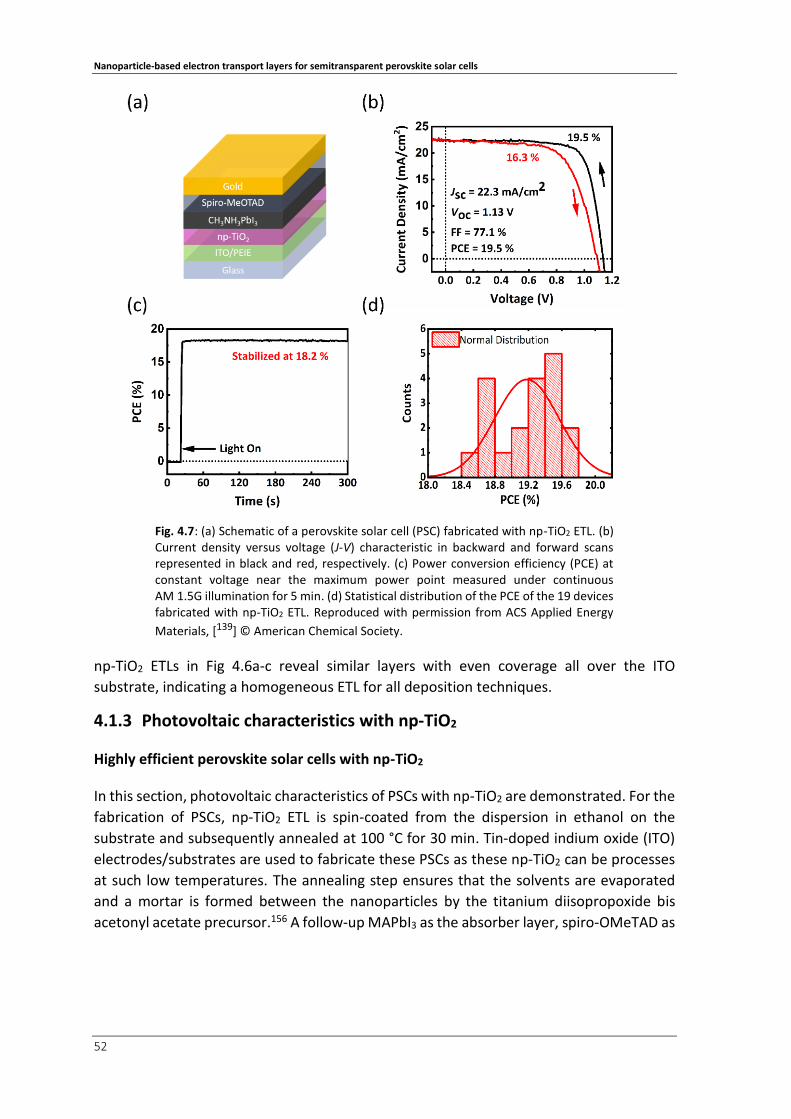
Nanoparticle-based electron transport layers for semitransparent perovskite solar cells
52
np-TiO2 ETLs in Fig 4.6a-c reveal similar layers with even coverage all over the ITO
substrate, indicating a homogeneous ETL for all deposition techniques.
4.1.3 Photovoltaic characteristics with np-TiO2
Highly efficient perovskite solar cells with np-TiO2
In this section, photovoltaic characteristics of PSCs with np-TiO2 are demonstrated. For the
fabrication of PSCs, np-TiO2 ETL is spin-coated from the dispersion in ethanol on the
substrate and subsequently annealed at 100 °C for 30 min. Tin-doped indium oxide (ITO)
electrodes/substrates are used to fabricate these PSCs as these np-TiO2 can be processes
at such low temperatures. The annealing step ensures that the solvents are evaporated
and a mortar is formed between the nanoparticles by the titanium diisopropoxide bis
acetonyl acetate precursor.156 A follow-up MAPbI3 as the absorber layer, spiro-OMeTAD as
Fig. 4.7: (a) Schematic of a perovskite solar cell (PSC) fabricated with np-TiO2 ETL. (b) Current density versus voltage (J-V) characteristic in backward and forward scans represented in black and red, respectively. (c) Power conversion efficiency (PCE) at constant voltage near the maximum power point measured under continuous AM 1.5G illumination for 5 min. (d) Statistical distribution of the PCE of the 19 devices fabricated with np-TiO2 ETL. Reproduced with permission from ACS Applied Energy
Materials, [139] © American Chemical Society.

Nanoparticle-based electron transport layers for semitransparent perovskite solar cells
53
hole transport layer and a rear Au electrode completes the opaque device as illustrated in
Fig. 4.7a.
The current-density versus voltage (J–V) measurements under air-mass 1.5 global
(AM 1.5G) illumination of the champion solar cell exhibit a JSC of 22.3 mA/cm2, a VOC of
1.13 V and a fill factor (FF) of 77.1%, leading to a PCE of 19.5% when measured from VOC
to JSC, i.e., backward scan (Fig. 4.7). The performance of the devices is reproducible, and
an average of 19 devices resulted in a PCE of approximately 19.2% as shown in Fig. 4.7d.
The apparent hysteresis leads to a reduced PCE of 16.3% when measured in the forward
direction, i.e., JSC to VOC. The hysteresis is often observed in n-i-p architecture of PSCs
employing compact ETLs and the origin of it is usually associated to trapping of charges
and ion migrations as discussed in chapter 2, section 2.5.119,157,158 In order to obtain the
real output power of the PSC, stabilized power output at constant illumination, close to
the maximum power point (MPP), is measured. The immediate rise of the PCE to 18.2%
(average of 19 devices, ≈17.4%) as shown in Fig. 4.7c and negligible drop in the efficiency
over 5 mins demonstrate that the np-TiO2 ETLs are an excellent material for PSCs. Overall,
these results show that nanoparticle based TiO2 ETLs deposited at low temperatures can
Fig. 4.8: Cross-section scanning electron microscopy image of perovskite solar cells with (a) thin (≈30-35 nm) and (b) thick (≈70-75 nm) np-TiO2 electron transport layers. Statistical distribution of (c) power conversion efficiency (PCE), (d) open-circuit voltage (VOC), and fill factor (FF) of perovskite solar cells with undoped (0%) and doped (7%) np-TiO2 as a thin (triangle, ≈30–35 nm) and thick (round, ≈70–75 nm) electron transport layers. Reproduced with permission from ACS Applied Energy Materials,
[139] © American Chemical Society.

Nanoparticle-based electron transport layers for semitransparent perovskite solar cells
54
yield highly efficient PSCs and potentially be used on flexible substrates for roll-to roll
processing.
Doping of np-TiO2 enables thick electron transport layers
A remarkable feature of the in-house synthesis is the feasibility of doping the np-TiO2 with
Nb5+ as discussed previously, which leads to an enhancement in the conductivity of the
np-TiO2 ETLs. Increased conductivity is crucial for rough substrates, which requires thick
ETLs to ensure a closed and compact film and avoids formation of shunts within the device.
Furthermore, for large-scale fabrications, thicker layers are beneficial as they are more
lenient to variations and inaccuracies of the deposition process. To demonstrate the
importance of doping, np-TiO2 electron transport thin (≈30–35 nm) and thick (≈70–75 nm)
layers are deposited to fabricate PSCs (Fig. 4.8a-b). Ideally, a thick np-TiO2 layer would
impede the transport of the charges compared to a thin np-TiO2 ETL and affect the FF of
the device. This is seen here as a reduction in both the FF and PCE (by ≈1.5%), for the
undoped np-TiO2 (compare red triangles and red circles in Fig. 4.8a-b). For the np-TiO2
doped with Nb5+, instead of a reduction in the FF for the thicker layer, a slightly improved
FF is noted (compare blue triangles and blue circles in Fig. 4.8a-b). The improved FF here
for the thicker layers is a direct consequence of the increased conductance of the ETL due
to the doping of np-TiO2 as discussed in the section 4.1.2. Furthermore, the VOC is also
improved, which might be associated to the increased thickness of the ETL. Overall, these
findings show that doping of the np-TiO2 is crucial for PSCs where thick ETLs are applicable.
Robustness of np-TiO2 electron transport layer
Another advantage of the in-house synthesis of np-TiO2 is the feasibility to control the size
of the np-TiO2 as described earlier. The size will in turn influence the surface topography
and the thickness of the ETL. PSCs fabricated with different sizes of np-TiO2 show the
Fig. 4.9: (a) Current density-voltage (J–V) characteristics and statistical distribution of the power conversion efficiency (PCE) for PSCs with np-TiO2 ETL hydrodynamic diameter/size of 9 nm, 20 nm, 22 nm, and 36 nm. A critical threshold size of the nanoparticles exits for efficient PSCs. Reproduced with permission from ACS Applied
Energy Materials, [139] © American Chemical Society.

Nanoparticle-based electron transport layers for semitransparent perovskite solar cells
55
existence of a critical threshold size of the nanoparticles for efficient PSCs (Fig. 4.9). For
np-TiO2 with a size > 20 nm, comparable performance (PCE ≈18%) is achieved. This
indicates that np-TiO2 with a wide size range can be used to fabricate PSCs with similar
PCEs, indicating the robustness of this ETL for PSCs. Nevertheless, for np-TiO2 with a size
< 20 nm, the PSCs exhibit low PCE ≈9%, mainly due to the poorer FF, lower VOC and a “S”-
shape in the J–V characteristic curve. One of the reasons for the poor performance of the
PSCs with smaller np-TiO2 ETL could be the lower electron mobility of the amorphous
phase of the np-TiO2 compared to its anatase phase.147
Compatibility of np-TiO2 electron transport layer with up scalable deposition techniques
In the previous section, homogeneous ETL with uniform coverage of np-TiO2 ETL is
deposited for various deposition techniques. Furthermore, perovskite absorbers deposited
on these layers demonstrate comparable surface morphologies and grain sizes (see
Appendix, Fig. A. 4.2). In order to compare the influence of these ETLs on the performance
of PSCs, devices are fabricated based on np-TiO2 ETL deposited using scalable inkjet
printing and slot-die coating techniques. The devices are fabricated in two different
Fig. 4.10: Statistical distribution of the power conversion efficiency (PCE) in (a) and (c) for PSCs with np-TiO2 ETL deposited with spin coating, inkjet printing and slot-die coating. PCE at constant voltage near the maximum power point measured under continuous AM 1.5G illumination for 5 min is also represented in (b) and (d).
Reproduced with permission from ACS Applied Energy Materials, [139] © American
Chemical Society.
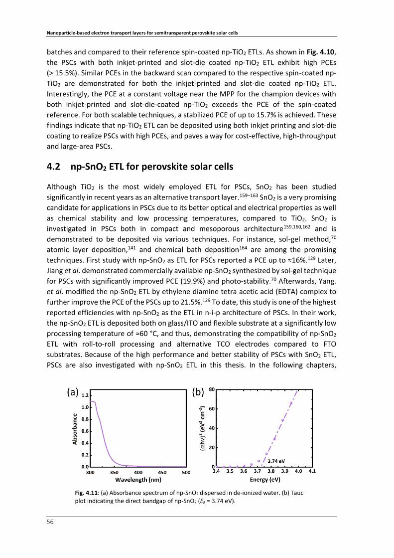
Nanoparticle-based electron transport layers for semitransparent perovskite solar cells
56
batches and compared to their reference spin-coated np-TiO2 ETLs. As shown in Fig. 4.10,
the PSCs with both inkjet-printed and slot-die coated np-TiO2 ETL exhibit high PCEs
(> 15.5%). Similar PCEs in the backward scan compared to the respective spin-coated np-
TiO2 are demonstrated for both the inkjet-printed and slot-die coated np-TiO2 ETL.
Interestingly, the PCE at a constant voltage near the MPP for the champion devices with
both inkjet-printed and slot-die-coated np-TiO2 exceeds the PCE of the spin-coated
reference. For both scalable techniques, a stabilized PCE of up to 15.7% is achieved. These
findings indicate that np-TiO2 ETL can be deposited using both inkjet printing and slot-die
coating to realize PSCs with high PCEs, and paves a way for cost-effective, high-throughput
and large-area PSCs.
4.2 np-SnO2 ETL for perovskite solar cells
Although TiO2 is the most widely employed ETL for PSCs, SnO2 has been studied
significantly in recent years as an alternative transport layer.159–163 SnO2 is a very promising
candidate for applications in PSCs due to its better optical and electrical properties as well
as chemical stability and low processing temperatures, compared to TiO2. SnO2 is
investigated in PSCs both in compact and mesoporous architecture159,160,162 and is
demonstrated to be deposited via various techniques. For instance, sol-gel method,70
atomic layer deposition,141 and chemical bath deposition164 are among the promising
techniques. First study with np-SnO2 as ETL for PSCs reported a PCE up to ≈16%.129 Later,
Jiang et al. demonstrated commercially available np-SnO2 synthesized by sol-gel technique
for PSCs with significantly improved PCE (19.9%) and photo-stability.70 Afterwards, Yang.
et al. modified the np-SnO2 ETL by ethylene diamine tetra acetic acid (EDTA) complex to
further improve the PCE of the PSCs up to 21.5%.129 To date, this study is one of the highest
reported efficiencies with np-SnO2 as the ETL in n-i-p architecture of PSCs. In their work,
the np-SnO2 ETL is deposited both on glass/ITO and flexible substrate at a significantly low
processing temperature of ≈60 °C, and thus, demonstrating the compatibility of np-SnO2
ETL with roll-to-roll processing and alternative TCO electrodes compared to FTO
substrates. Because of the high performance and better stability of PSCs with SnO2 ETL,
PSCs are also investigated with np-SnO2 ETL in this thesis. In the following chapters,
Fig. 4.11: (a) Absorbance spectrum of np-SnO2 dispersed in de-ionized water. (b) Tauc plot indicating the direct bandgap of np-SnO2 (Eg = 3.74 eV).

Nanoparticle-based electron transport layers for semitransparent perovskite solar cells
57
np-SnO2 (bought commercially) is used as the ETL in its n-i-p architecture for PSCs. To
obtain further insights, the np-SnO2 are characterized and their properties are discussed
in light of this study and literature.
4.2.1 Material properties of np-SnO2 The np-SnO2 are commercially available from the chemical company Alfa Aesar. The
colloidal dispersion of the np-SnO2 is dispersed in water and has a concentration of ≈15%.
Spectrophotometric measurements are conducted to determine the bandgap of np-SnO2.
For this, a similar procedure is applied as for the np-TiO2. The absorbance spectra of the
np-SnO2 dispersion is shown in Fig. 4.11a. Using equation 4.1, the direct bandgap of the
np-SnO2 is determined to be 3.74 eV from the Tauc plot (Fig. 4.11b), which is in good
agreement with the literature.70 The np-SnO2 used in this study is characterized more in
detail in the work of Jiang et al.70 The np-SnO2 are stoichiometric and crystalline in nature
with a tetragonal SnO2 lattice structure.70 The size of the nanoparticles, determined with
transmission electron microscopy (TEM) in that study, is ≈3-4 nm.70 In the following
section, a comparison between the optical properties and the photovoltaic characteristics
of the PSCs fabricated with np-TiO2 and np-SnO2 ETLs is discussed.
4.3 Comparison between np-TiO2 and np-SnO2 ETL Both np-TiO2 and np-SnO2 exhibit promising material properties. In the following sections,
the ETLs deposited with np-TiO2 and np-SnO2 are characterized in more detail. Initial
studies include optical properties, photo physics and morphology of these layers. Finally,
both opaque perovskite solar cells (o-PSCs) and s-PSCs fabricated with these ETLs are
analyzed.
4.3.1 Optical properties, photo-physics and morphology
Ellipsometry measurements are performed on ETLs of np-TiO2 and np-SnO2 deposited on
glass to evaluate the optical constants (refractive index, n and extinction coefficient, k).
Fig. 4.12 shows the refractive index and the extinction coefficient of np-TiO2 and np-SnO2
Fig. 4.12: Optical constants (n, k) of np-TiO2 and np-SnO2.

Nanoparticle-based electron transport layers for semitransparent perovskite solar cells
58
layers. Both layers exhibit high refractive index (> 1.63) and is almost non-dispersive in the
wavelength range 400-1200 nm. Compared to np-TiO2 ETL, a higher refractive index is
noted for np-SnO2 ETL. The high extinction coefficient of the np-TiO2 ETL below 400 nm is
due to the smaller bandgap of the np-TiO2. Nevertheless, np-TiO2 exhibits significantly
higher extinction coefficient in the wavelength range 400-1200 nm, indicating that np-TiO2
ETL is susceptible to increased parasitic absorption losses in the PSCs, if thick layers are
used.
For the spectrophotometric measurements, the ETLs are deposited on glass/ITO
substrates, which is the TCO electrode for the PSCs. This measurement is carried out to
obtain the transmittance (T), and the reflectance (R) of the layers on glass/ITO/ETL with
glass/ITO as the reference stack (Fig. 4.13). T, R and A (calculated from Equation 3.3) of
the ITO layer are slightly modified when np-SnO2 are deposited atop (Fig. 4.13a-c). For
np-TiO2, the reflectance is reduced significantly, and a strong modification of the
interference peaks are observed. The reduction of the reflectance is due to a smaller
refractive index of the np-TiO2, resulting in a lower Fresnel reflection at the ETL/air
interface (Fig. 4.13a). Hence, the maximum of the transmittance is slightly increased
(Fig. 4.13b). The variation of the interference peak position indicates that the thickness of
the np-TiO2 ETL differs from the np-SnO2. Cross-sectional scanning electron microscopy
(SEM) conducted on both ETLs on ITO reveals that the np-TiO2 forming a compact layer on
top of the ITO with a thickness of ≈30-50 nm, while thickness of the np-SnO2 ETL stands
below 10 nm (Fig. 4.14).
Fig. 4.13: (a) Reflectance (R), (b) Transmittance (T) and (c) Absorptance (A) of the layer stacks: glass/ITO, glass/ITO/np-TiO2 and glass/ITO/np-SnO2.
Fig. 4.14: Cross-section scanning microscopy images of np-TiO2 and np-SnO2 on glass/ITO substrates.

Nanoparticle-based electron transport layers for semitransparent perovskite solar cells
59
The efficient extraction and transport of the electrons from the absorber layer to the
respective contact are the two important criteria of a good ETL. To investigate this,
steady-state photoluminescence (SSPL) and time-resolved photoluminescence (TRPL)
spectroscopy measurements are carried out on glass/np-TiO2/perovskite and
glass/np-SnO2/perovskite layers (Fig. 4.15). The samples are excited with a pulsed laser
with a wavelength of 532 nm (with energy above the bandgap of the perovskite absorber).
The TRPL shows an extremely fast decay of the photoluminescence with np-SnO2 as the
ETL, while a slow decay is detected for np-TiO2 (Fig. 4.15a). The corresponding lifetimes of
the charge carriers extracted by fitting to a stretched exponential function are of 38 ns and
133 ns for np-SnO2 and np-TiO2, respectively. The fast decay with the np-SnO2 ETL implies
that the electrons which are created upon excitation are immediately extracted by the ETL,
indicating a fast separation of electrons from the holes before they recombine radiatively
in the absorber layer or non-radiatively at defect/interfacial sites. The comparatively
longer lifetime and slow extraction with the np-TiO2 indicates the existence of an electron
barrier between the absorber and the ETL. This slow extraction of charges could be due to
the shallower conduction band or the lower electron mobility of TiO2 compared to np-SnO2
ETL.129,143,165 Nevertheless, the improved lifetime could also indicate a possible reduced
number of defects or traps within the perovskite absorber due to a better film
morphology.166 All these results are also in line with the SSPL measurements. Compared to
the np-TiO2 ETL, the photoluminescence intensity is reduced significantly with np-SnO2 ETL,
further indicating the superior mobility of the np-SnO2 ETL.
4.3.2 Photovoltaic characteristics of PSCs with nanoparticle-based ETL In this section, the photovoltaic parameters of o-PSCs and s-PSCs fabricated in a same
batch with np-TiO2 and np-SnO2 are discussed. The device stack is as follows:
glass/ITO/(np-TiO2 or np-SnO2)/MAPbI3/Spiro-OMeTAD/(Au or MoOX/ITO). The ETLs, np-
TiO2 and np-SnO2 are deposited at low annealing temperatures of 100 °C and 150 °C,
respectively. For the fabrication of s-PSCs, a thin 10 nm MoOX buffer layer is used to
prevent damage to the underlying Spiro-OMeTAD or the perovskite absorber upon
sputtering. It should be noted that the overall performance of this specific batch of samples
is comparatively low, mainly due to the use of old precursor materials and solvents. The
Fig. 4.15: (a) Time-resolved and (b) steady-state photoluminescence spectra of layer stack: glass/np-TiO2/perovskite and glass/np-SnO2/perovskite.
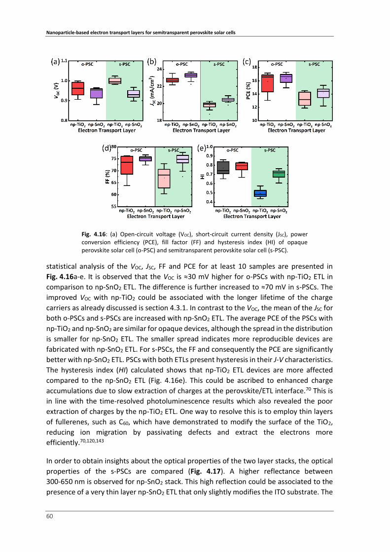
Nanoparticle-based electron transport layers for semitransparent perovskite solar cells
60
statistical analysis of the VOC, JSC, FF and PCE for at least 10 samples are presented in
Fig. 4.16a-e. It is observed that the VOC is ≈30 mV higher for o-PSCs with np-TiO2 ETL in
comparison to np-SnO2 ETL. The difference is further increased to ≈70 mV in s-PSCs. The
improved VOC with np-TiO2 could be associated with the longer lifetime of the charge
carriers as already discussed is section 4.3.1. In contrast to the VOC, the mean of the JSC for
both o-PSCs and s-PSCs are increased with np-SnO2 ETL. The average PCE of the PSCs with
np-TiO2 and np-SnO2 are similar for opaque devices, although the spread in the distribution
is smaller for np-SnO2 ETL. The smaller spread indicates more reproducible devices are
fabricated with np-SnO2 ETL. For s-PSCs, the FF and consequently the PCE are significantly
better with np-SnO2 ETL. PSCs with both ETLs present hysteresis in their J-V characteristics.
The hysteresis index (HI) calculated shows that np-TiO2 ETL devices are more affected
compared to the np-SnO2 ETL (Fig. 4.16e). This could be ascribed to enhanced charge
accumulations due to slow extraction of charges at the perovskite/ETL interface.70 This is
in line with the time-resolved photoluminescence results which also revealed the poor
extraction of charges by the np-TiO2 ETL. One way to resolve this is to employ thin layers
of fullerenes, such as C60, which have demonstrated to modify the surface of the TiO2,
reducing ion migration by passivating defects and extract the electrons more
efficiently.70,120,143
In order to obtain insights about the optical properties of the two layer stacks, the optical
properties of the s-PSCs are compared (Fig. 4.17). A higher reflectance between
300-650 nm is observed for np-SnO2 stack. This high reflection could be associated to the
presence of a very thin layer np-SnO2 ETL that only slightly modifies the ITO substrate. The
Fig. 4.16: (a) Open-circuit voltage (VOC), short-circuit current density (JSC), power conversion efficiency (PCE), fill factor (FF) and hysteresis index (HI) of opaque perovskite solar cell (o-PSC) and semitransparent perovskite solar cell (s-PSC).

Nanoparticle-based electron transport layers for semitransparent perovskite solar cells
61
transmittance spectra with both ETLs are comparable, with strong interferences and a
maximum transmittance of ~75% is achieved. The low transmission above 1000 nm is due
to the high reflection (Fig. 4.17a) and strong parasitic absorptions (Fig. 4.18c) for both the
stacks. The absorptance of 20-30% in the near infrared wavelengths below the bandgap of
the perovskite absorber is due to the parasitic losses associated with the front ITO and rear
ITO. Detailed discussion and several strategies to overcome this are discussed in Chapter
5 and Chapter 6. The comparatively improved transmittance in the near infrared
wavelengths with the np-SnO2 ETL stack is due to the reduced absorptance, which is in line
with the measured extinction coefficients of the two ETLs.
To determine the real power of the PSCs fabricated with both np-TiO2 and np-SnO2, the
fabricated devices are characterized by MPP tracking (Fig. 4.18a). PSCs with both ETLs
remain stable during the course of these measurements. Moreover, a small increase in the
PCE is observed for the np-SnO2, which is due to the light soaking effect.167 Long-term
stability and shelf lifetime are also investigated for PSCs fabricated with np-TiO2 and np-
SnO2 ETLs. Here, instead of MAPbI3 as the absorber layer, triple cation (TC) perovskite
absorber based on FA, MA and Cs is used, which is reported to be intrinsically more stable
than MAPbI3.32 For this, o-PSCs are fabricated for both the architectures and the MPP at
constant voltage near the maximum power is measured over several days. It is shown that
devices with np-TiO2 show a decay in the power output and remain unstable on day 1 (Fig.
4.18b-c). However, they tend to stabilize and improve in PCE with time. In contrast,
np-SnO2 based devices are stable from day 1. The observed improvement in the PCE is
independent of the ETL and is related to the reduction in trap-assisted non-radiative
recombination and strain relaxation in the triple cation perovskite absorber.168
4.4 Discussions and conclusion
In this chapter, alternative ETLs (np-TiO2 and np-SnO2) are investigated for fabricating PSCs
with the aim to reduce the depositing temperature of the ETL. Compared to the most
widely used ETL (mesoporous TiO2), which requires high annealing temperatures
(> 450 °C),31–34 these ETLs require processing temperatures of below 150 °C. The reason
behind this low processing temperature is the pre-synthesis of TiO2 and SnO2 into their
crystalline form. Furthermore, due to low processing temperatures of these ETLs, the
Fig. 4.17: (a) Reflectance (R), (b) transmittance (T) and (c) absorptance (A) of the semitransparent perovskite solar cell (s-PSC) layer stack with np-TiO2 and np-SnO2 electron transport layers.
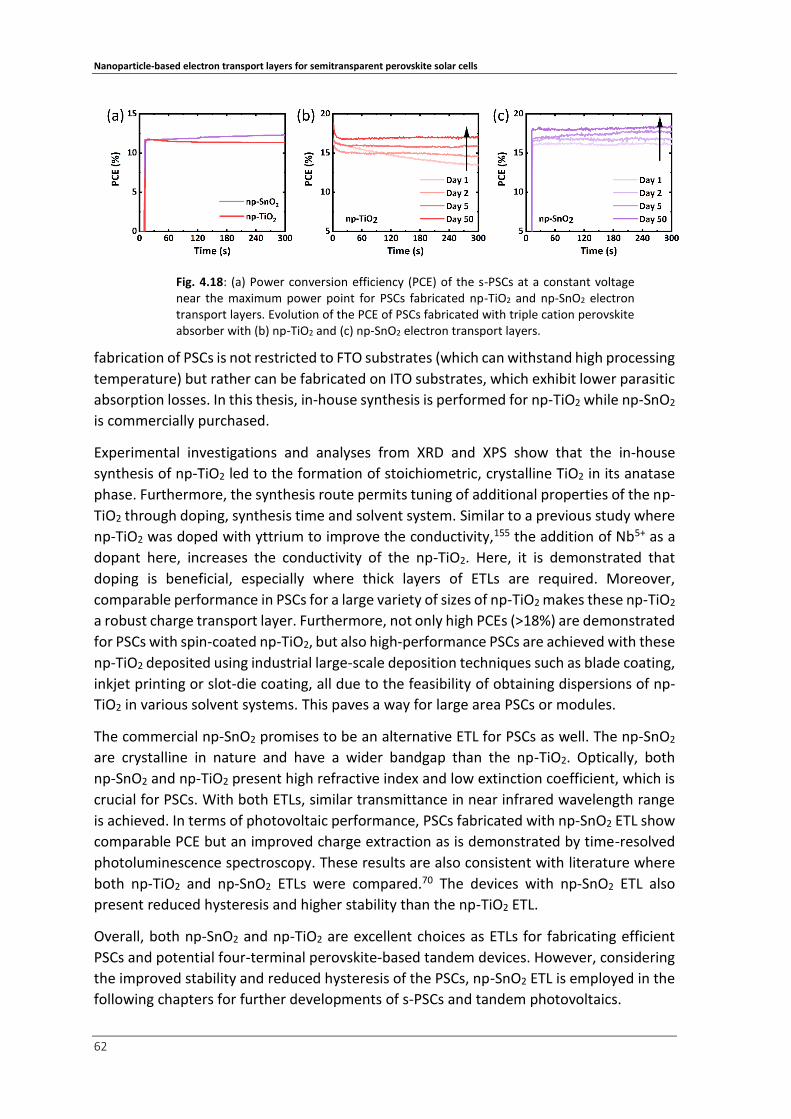
Nanoparticle-based electron transport layers for semitransparent perovskite solar cells
62
fabrication of PSCs is not restricted to FTO substrates (which can withstand high processing
temperature) but rather can be fabricated on ITO substrates, which exhibit lower parasitic
absorption losses. In this thesis, in-house synthesis is performed for np-TiO2 while np-SnO2
is commercially purchased.
Experimental investigations and analyses from XRD and XPS show that the in-house
synthesis of np-TiO2 led to the formation of stoichiometric, crystalline TiO2 in its anatase
phase. Furthermore, the synthesis route permits tuning of additional properties of the np-
TiO2 through doping, synthesis time and solvent system. Similar to a previous study where
np-TiO2 was doped with yttrium to improve the conductivity,155 the addition of Nb5+ as a
dopant here, increases the conductivity of the np-TiO2. Here, it is demonstrated that
doping is beneficial, especially where thick layers of ETLs are required. Moreover,
comparable performance in PSCs for a large variety of sizes of np-TiO2 makes these np-TiO2
a robust charge transport layer. Furthermore, not only high PCEs (>18%) are demonstrated
for PSCs with spin-coated np-TiO2, but also high-performance PSCs are achieved with these
np-TiO2 deposited using industrial large-scale deposition techniques such as blade coating,
inkjet printing or slot-die coating, all due to the feasibility of obtaining dispersions of np-
TiO2 in various solvent systems. This paves a way for large area PSCs or modules.
The commercial np-SnO2 promises to be an alternative ETL for PSCs as well. The np-SnO2
are crystalline in nature and have a wider bandgap than the np-TiO2. Optically, both
np-SnO2 and np-TiO2 present high refractive index and low extinction coefficient, which is
crucial for PSCs. With both ETLs, similar transmittance in near infrared wavelength range
is achieved. In terms of photovoltaic performance, PSCs fabricated with np-SnO2 ETL show
comparable PCE but an improved charge extraction as is demonstrated by time-resolved
photoluminescence spectroscopy. These results are also consistent with literature where
both np-TiO2 and np-SnO2 ETLs were compared.70 The devices with np-SnO2 ETL also
present reduced hysteresis and higher stability than the np-TiO2 ETL.
Overall, both np-SnO2 and np-TiO2 are excellent choices as ETLs for fabricating efficient
PSCs and potential four-terminal perovskite-based tandem devices. However, considering
the improved stability and reduced hysteresis of the PSCs, np-SnO2 ETL is employed in the
following chapters for further developments of s-PSCs and tandem photovoltaics.
Fig. 4.18: (a) Power conversion efficiency (PCE) of the s-PSCs at a constant voltage near the maximum power point for PSCs fabricated np-TiO2 and np-SnO2 electron transport layers. Evolution of the PCE of PSCs fabricated with triple cation perovskite absorber with (b) np-TiO2 and (c) np-SnO2 electron transport layers.
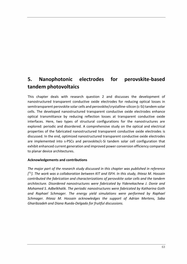
63
5. Nanophotonic electrodes for perovskite-based
tandem photovoltaics
This chapter deals with research question 2 and discusses the development of
nanostructured transparent conductive oxide electrodes for reducing optical losses in
semitransparent perovskite solar cells and perovskite/crystalline-silicon (c-Si) tandem solar
cells. The developed nanostructured transparent conductive oxide electrodes enhance
optical transmittance by reducing reflection losses at transparent conductive oxide
interfaces. Here, two types of structural configurations for the nanostructures are
explored: periodic and disordered. A comprehensive study on the optical and electrical
properties of the fabricated nanostructured transparent conductive oxide electrodes is
discussed. In the end, optimized nanostructured transparent conductive oxide electrodes
are implemented into s-PSCs and perovskite/c-Si tandem solar cell configuration that
exhibit enhanced current generation and improved power conversion efficiency compared
to planar device architectures.
Acknowledgements and contributions
The major part of the research study discussed in this chapter was published in reference
[71]. The work was a collaboration between KIT and ISFH. In this study, Ihteaz M. Hossain
contributed the fabrication and characterizations of perovskite solar cells and the tandem
architecture. Disordered nanostructures were fabricated by Yidenekachew J. Donie and
Mohamed S. Adbelkhalik. The periodic nanostructures were fabricated by Katharina Goth
and Raphael Schmager. The energy yield simulations were performed by Raphael
Schmager. Ihteaz M. Hossain acknowledges the support of Adrian Mertens, Saba
Gharibzadeh and Diana Rueda-Delgado for fruitful discussions.

Nanophotonic electrodes for perovskite-based tandem photovoltaics
64
Recently, perovskite-based tandem photovoltaics received a lot of attention in the
scientific community. This is due to the wide bandgap of the lead-based organic-inorganic
perovskite as the top cell’s absorber. Tremendous progress has been made in the last
decade and as a result, the power conversion efficiency (PCE) of the current
state-of-the-art perovskite/crystalline-silicon (c-Si) tandem solar cell already reached
29.1% in two-terminal tandem architecture.10 Although the PCE of perovskite/c-Si tandem
solar cell obtained is remarkable various optical losses including reflection losses at
interfaces, reduced transmission of the top cell due to parasitic absorption within the
layers are some of the bottlenecks that needs to be overcome.25,38,169,170
Light management concepts are typically employed to overcome the optical losses.15 Both
micron- and nano-scale textures have been demonstrated for perovskite solar cells (PSCs)
for reducing the optical losses. The micron-scale textures, which is commonly employed at
the front air/glass interface allow the light to undergo multiple interactions with the
textured surface and increase the probability for light in-coupling.58–63 The potential of
micro-textures with different geometries such as regular pyramids,60 inverted pyramids,134
cones,62,171 and random textures58,63 were investigated as light in-coupling element into
PSCs, which lead to a 4% reduction in reflection losses in most cases. In contrast to
micron-scale textures, nano-scale textures can be easily integrated into the thin film layers
of PSCs.41,42,64,65,69,172–177 Investigated textures include nanophotonic front and rear
electrodes,41,64,65 patterned charge transport,173,174 corrugated substrates,172,177 and active
perovskite layers.69,175,176 The nanophotonic front electrodes, the charge transport layers
and the corrugated substrates reduce reflection losses by introducing a gradual matching
of the refractive index forming a so-called effective refractive index medium, thus
suppressing the Fresnel reflection losses.41,173,174 The textured rear electrode also
improves light absorption through scattering and surface plasmonic resonance excited by
the corrugation.65 Patterned active layers demonstrate improved light absorption by
enhancing the light-coupling to the quasi-guided modes of the perovskite absorber.69,175,176
Previous studies have also demonstrated that nanophotonic front electrodes enhance
optical transmittance and reduce reflectance both in the visible and near-infrared
wavelength ranges.72 They demonstrated an improvement of 8% absolute.72 Therefore,
nanotexturing a TCO would not only be beneficial for both opaque single junction PSC, but
also be compelling for perovskite-based tandem architectures. However, these
nanostructures are yet to be explored for semitransparent perovskite solar cells (s-PSCs)
and tandem architectures in real prototype devices.
In this chapter, nanostructured tin-doped indium oxide (NS ITO) electrode is employed in
s-PSCs and in 4T tandem perovskite/c-Si tandem architecture. These nanostructured ITO
reduce the prominent reflection losses at the ITO interfaces as discussed earlier in
chapter 2, section 2.5 and improve the transmission. Two configurations of NS ITO are
investigated: periodic and disordered. In the follow-up sections, detailed optical and
electrical properties of the NS ITO and PSCs fabricated with NS ITO are discussed.

Nanophotonic electrodes for perovskite-based tandem photovoltaics
65
5.1 Periodic nanophotonic electrodes This section discusses morphological, optical and electrical properties of periodic NS ITO
for improved light in-coupling. The morphological properties are obtained with atomic
force microscopy (AFM). Spectrophotometric measurements are performed to determine
the optical responses of these NS ITO. The fabricated NS ITO electrodes are also
characterized by four-point probe technique to determine their electrical properties.
Morphology and opto-electronic properties of periodic NS ITO
The periodic nanostructured ITO comprises of nanopillars made of a polymer material
called OrmoComp deposited in an ordered fashion with a constant periodicity by
soft-imprinting of polymers using molds of nanostructures (Fig. 5.1). A follow-up
Fig. 5.1: Schematic illustration of periodic nanostructured TCO: (a) side-view and (b) top-view. The periodic nanostructures have a height h and are separated with a periodicity of p. Up on deposition of a transparent conductive oxide (TCO) electrode conformally, periodic nanostructured TCO electrodes are obtained.
Fig. 5.2: Atomic force microscopy images of nanostructured ITO electrode fabricated with soft-imprinting for periods, p = 200 nm, 300 nm, 400 nm and 500 nm.
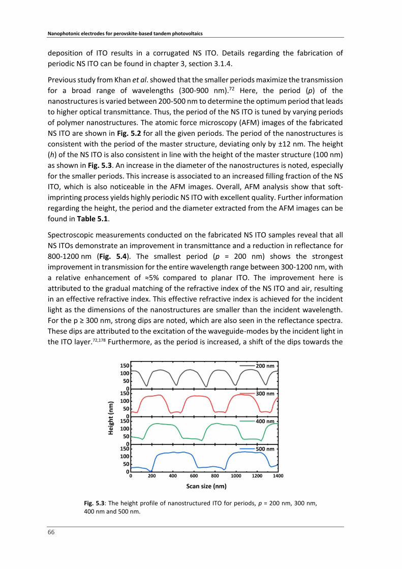
Nanophotonic electrodes for perovskite-based tandem photovoltaics
66
deposition of ITO results in a corrugated NS ITO. Details regarding the fabrication of
periodic NS ITO can be found in chapter 3, section 3.1.4.
Previous study from Khan et al. showed that the smaller periods maximize the transmission
for a broad range of wavelengths (300-900 nm).72 Here, the period (p) of the
nanostructures is varied between 200-500 nm to determine the optimum period that leads
to higher optical transmittance. Thus, the period of the NS ITO is tuned by varying periods
of polymer nanostructures. The atomic force microscopy (AFM) images of the fabricated
NS ITO are shown in Fig. 5.2 for all the given periods. The period of the nanostructures is
consistent with the period of the master structure, deviating only by ±12 nm. The height
(h) of the NS ITO is also consistent in line with the height of the master structure (100 nm)
as shown in Fig. 5.3. An increase in the diameter of the nanostructures is noted, especially
for the smaller periods. This increase is associated to an increased filling fraction of the NS
ITO, which is also noticeable in the AFM images. Overall, AFM analysis show that soft-
imprinting process yields highly periodic NS ITO with excellent quality. Further information
regarding the height, the period and the diameter extracted from the AFM images can be
found in Table 5.1.
Spectroscopic measurements conducted on the fabricated NS ITO samples reveal that all
NS ITOs demonstrate an improvement in transmittance and a reduction in reflectance for
800-1200 nm (Fig. 5.4). The smallest period (p = 200 nm) shows the strongest
improvement in transmission for the entire wavelength range between 300-1200 nm, with
a relative enhancement of ≈5% compared to planar ITO. The improvement here is
attributed to the gradual matching of the refractive index of the NS ITO and air, resulting
in an effective refractive index. This effective refractive index is achieved for the incident
light as the dimensions of the nanostructures are smaller than the incident wavelength.
For the p ≥ 300 nm, strong dips are noted, which are also seen in the reflectance spectra.
These dips are attributed to the excitation of the waveguide-modes by the incident light in
the ITO layer.72,178 Furthermore, as the period is increased, a shift of the dips towards the
Fig. 5.3: The height profile of nanostructured ITO for periods, p = 200 nm, 300 nm, 400 nm and 500 nm.

Nanophotonic electrodes for perovskite-based tandem photovoltaics
67
higher wavelengths is also noted. Thus, by tuning the periodicity, a desired transmittance
for a particular range of wavelengths can also be obtained. For the application in tandem
photovoltaics, the smallest periodicity should be preferred as the improvement is for a
wide range of wavelengths. Overall, the findings show that with NS ITO, reflection losses
are effectively reduced, and the transmittance is improved significantly.
The improved light in-coupling for NS ITO results in a tradeoff in increased sheet resistance.
Higher sheet resistance (approximately 4 times) is noted for NS ITO with the smallest
period that demonstrated the maximum transmittance in comparison to the planar ITO.
The increased sheet resistance could be associated to possible cracks, increased surface
area or number of grain boundaries in the ITO.179 The measurement also shows that the
periodicity of the NS ITO influences the sheet resistance. As the period is increased, the
Fig. 5.4: (a) Transmittance (T), (b) reflectance (R) and (c) sheet resistance (Rsh) of the nanostructured ITO electrode ITO for periods, p = 200 nm, 300 nm, 400 nm and 500 nm.

Nanophotonic electrodes for perovskite-based tandem photovoltaics
68
sheet resistance drops from 96 Ω/sq to 50 Ω/sq for periods up to 400 nm. For 500 nm, the
sheet resistance increases which could be related to the inhomogeneous sputtering of the
ITO.132 Overall, these results show that both transmission and sheet resistance of the
fabricated NS ITO are intertwined and suggest that a balance must be obtained between
the optical and the electrical peroperties of the NS ITO so that an overall improvement is
achieved in the performance of perovskite-based tandem devices.
Table 5.1: The period (p), height (h), measured diameter and theoretical diameter of the nanostructured ITO electrode ITO for periods, p = 200 nm, 300 nm, 400 nm and 500 nm.
Master
Structure (nm) p (nm) h (nm)
Measured
diameter (nm)
Theoretical
diameter (nm)
200 191 90 230 134
300 296 100 267 200
400 388 95 300 268
500 506 100 386 335
5.2 Disordered nanophotonic electrodes This section discusses morphological, optical and electrical and properties disordered NS
ITO for improved transmittance. The morphological properties are investigated with AFM
and scanning electron microcopy (SEM). Spectrophotometric measurements are
performed to determine the optical responses of the disordered NS ITO. The fabricated NS
ITOs are characterized by four-point probe technique to determine their sheet resistances.
Morphology and opto-electronic properties of disordered NS ITO
A schematic of the side-view and the top-view of the disordered nanostructured TCO
electrode is depicted in Fig. 5.5. In contrast to the periodic NS ITO, the nanostructures in
the disordered NS ITO are oriented randomly and with a certain average inter-distance
Fig. 5.5: Schematic of disordered nanostructured TCO: (a) side-view and (b) top-view.
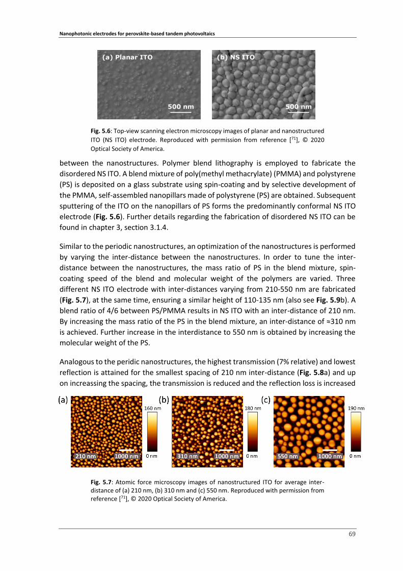
Nanophotonic electrodes for perovskite-based tandem photovoltaics
69
between the nanostructures. Polymer blend lithography is employed to fabricate the
disordered NS ITO. A blend mixture of poly(methyl methacrylate) (PMMA) and polystyrene
(PS) is deposited on a glass substrate using spin-coating and by selective development of
the PMMA, self-assembled nanopillars made of polystyrene (PS) are obtained. Subsequent
sputtering of the ITO on the nanopillars of PS forms the predominantly conformal NS ITO
electrode (Fig. 5.6). Further details regarding the fabrication of disordered NS ITO can be
found in chapter 3, section 3.1.4.
Similar to the periodic nanostructures, an optimization of the nanostructures is performed
by varying the inter-distance between the nanostructures. In order to tune the inter-
distance between the nanostructures, the mass ratio of PS in the blend mixture, spin-
coating speed of the blend and molecular weight of the polymers are varied. Three
different NS ITO electrode with inter-distances varying from 210-550 nm are fabricated
(Fig. 5.7), at the same time, ensuring a similar height of 110-135 nm (also see Fig. 5.9b). A
blend ratio of 4/6 between PS/PMMA results in NS ITO with an inter-distance of 210 nm.
By increasing the mass ratio of the PS in the blend mixture, an inter-distance of ≈310 nm
is achieved. Further increase in the interdistance to 550 nm is obtained by increasing the
molecular weight of the PS.
Analogous to the peridic nanostructures, the highest transmission (7% relative) and lowest
reflection is attained for the smallest spacing of 210 nm inter-distance (Fig. 5.8a) and up
on increassing the spacing, the transmission is reduced and the reflection loss is increased
Fig. 5.6: Top-view scanning electron microscopy images of planar and nanostructured
ITO (NS ITO) electrode. Reproduced with permission from reference [71], © 2020
Optical Society of America.
Fig. 5.7: Atomic force microscopy images of nanostructured ITO for average inter-distance of (a) 210 nm, (b) 310 nm and (c) 550 nm. Reproduced with permission from reference [71], © 2020 Optical Society of America.

Nanophotonic electrodes for perovskite-based tandem photovoltaics
70
(300-700 nm). The relative enhancement with the lowest inter-distance is slightly higher
for disordered NS ITO than the periodic NS ITO. This higher enhancement might be due to
the difference in the refrative index of PS and OrmoComp, which act as the nanopillars for
disordered and planar NS ITO, respectively. However, further investigations are necessary
by fabricating and comparaing both types of TCOs in a same batch. Another apparent
difference to the peridic NS ITO is the absence of dips in the transmittace or the reflectance
spectra. Rather, a broadband drop is observed, which is due to the wide distribution of size
of the nanopillars in disorderd NS ITO (see Fig. 5.9a and also Fig. 5.4 and Fig. 5.8
transmittance spectra). This absence is attributed to the excitation of the leaky modes for
a wide range of wavelengths (below the periodicty) instead of specific k-vectors, which is
present for periodic NS ITO.180
Electrically, the sheet resistance (Rsh) is also influenced by the spacing of the
nanostructures similar to the periodic nanostructures. Thus, the smallest spacing - 210 nm
shows the highest sheet resistance. Overall, these results indicate that employing
nanostructures enable a path to improve the optical properties for the application of solar
Fig. 5.9: (a) Statistical analysis of the (a) diameter of the nanostructures and (b) the height profile of nanostructured ITO electrode for 210 nm spacing derived from AFM measurement. Reproduced with permission from reference [71], © 2020 Optical Society of America.
Fig. 5.8: (a) Transmittance (T) and reflectance (R) represented by solid and dashed lines, respectively, of various nanostructured ITO and (b) their corresponding sheet resistances (Rsh). Reproduced with permission from reference [71], © 2020 Optical Society of America.

Nanophotonic electrodes for perovskite-based tandem photovoltaics
71
cells, however, with a trade-off in the electrical properties. In the following section, s-PSCs
are fabricated and the performance of perovskite-based tandem devices with
nanostructures are explored.
5.3 Photovoltaic characteristics of perovskite solar cells with
nanostructured ITO In this section, the photovoltaic performances of the fabricated s-PSCs and the 4T
perovskite/c-Si tandem solar cell are demonstrated with NS ITO. Based on the previous
observations, both periodic and disordered NS ITO having the smallest period or
inter-distance of ≈200 nm demonstrated the highest transmittance. However, with
disordered NS ITO, the relative enhancement is slightly higher than the periodic one. In
addition to this, the fabrication of the disordered NS ITO involves fewer steps in
comparison to the periodic NS ITO. Moreover, in a recent submitted study by Donie et al.,
it is shown that the disordered nanopillars of PS can be deposited by inkjet printing, which
is beneficial for upscaling, cost-effectiveness and flexibility in design.181 Therefore, in this
study, s-PSCs are fabricated with disordered NS ITO with the smallest spacing that depicted
the highest transmittance.
5.3.1 Semitransparent perovskite and perovskite/c-Si tandem solar cells
In order to evaluate the performance of perovskite/c-Si tandem solar with NS ITO, s-PSCs
are fabricated with the following layer stack: glass/planar ITO or NS ITO/np-SnO2/
perovskite/spiro-MeOTAD/MoOX/ITO (Fig. 5.10a,b). A triple cation perovskite layer is
deposited as the absorber layer. Cross-section SEM image shows a homogenous perovskite
absorber layer is formed on the nanostructured electrode, which is also structured.
However, a planarization is achieved for subsequent layer stack. The semitransparent
devices are completed by the hole transport layer spiro-MeOTAD, a MoOX buffter layer
and a rear ITO.
The current density-voltage (J-V) characteristics of the champion device is depicted in
Fig. 5.11a. The s-PSC demonstrate an improved short-circuit current density (JSC) of ≈2%
compared to the planar reference. The improved JSC is attributed to the reduction of the
reflection losses and increased absorption above the bandgap (300-760 nm) of the
perovskite absorber (Fig. 5.11c). The improved JSC is also reflected in the external quantum
efficiency (EQE) measurement (Fig. 5.11b). In accordance to the improved absorptance
(Fig. 5.11c), an enhanced EQE over a broad spectral range is observed. The improvement
Fig. 5.10: Cross-section scanning electron microscopy (SEM) image of (a) nanostructured and (b) planar s-PSCs. Adapted with permission from reference [71], © 2020 Optical Society of America.

Nanophotonic electrodes for perovskite-based tandem photovoltaics
72
in the JSC is also consistent for more than one investigated sample and different bandgaps
of the perovskite absorber layer. Six samples fabricated in two separate batches for two
different bandgaps show an improvement of approximately 3% (average) in the JSC (Fig.
5.12 and Appendix, Fig. A. 5.1). Overall, these results show that reducing the reflection
losses by nano structuring the ITO leads to an improvement in the JSC of the fabricated
PSCs.
Although the JSC obtained with NS ITO electrodes surpasses the JSC of the planar ITO
electrodes, both the open-circuit voltage (VOC) and the FF are affected (see Appendix,
Fig. 5.11: (a) Current density-voltage characteristics and (b) external quantum efficiency (EQE) of semitransparent perovskite solar cells (s-PSCs) fabricated with nanostructured (NS) and planar ITO electrode, crystalline-silicon (c-Si) solar cell measured stand-alone configuration and under filters of s-PSCs with NS and planar ITO electrode. (c) Reflectance (R), Transmittance (T) and absorptance (A) of filters of s-PSCs with NS and planar ITO electrode. Adapted with permission from reference [71], © 2020 Optical Society of America.

Nanophotonic electrodes for perovskite-based tandem photovoltaics
73
Fig. A. 5.2 for further details). The VOC is reduced by ∼40 mV and the FF drops by 5%
(Fig. 5.11a). Time-resolved photoluminescence measurement in Fig. 5.13 shows a fast
decay in the photoluminescence, indicating a reduced lifetime of the charge carriers in the
NS ITO electrode-based device. This suggests a higher non-radiative recombination
processes at the interface of NS ITO/np-SnO2 or np-SnO2/perovskite. The drop in the FF is
associated to a slight observable shunt and an increase in the series resistance in the J-V
characteristic of the PSC (series resistance with planar ITO: 70.2 Ω and series resistance
NS ITO-PSC: 81.4 Ω). The increased series resistance can be attributed to the increased Rsh
discussed earlier, which can mainly originate from the cracks that appear in the NS ITO
(see Fig. 5.10a). Although the impact of the increased Rsh is not so severe in these
fabricated s-PSCs (due to the small active area of 10.5 mm2), the effect will not be
insignificant for large area devices or modules. Therefore, further investigations are
needed to reduce this loss. Overall, due to the reduction of both VOC and the FF, the PCE
of the s-PSC with NS ITO electrode is decreased compared to the planar reference, leading
to 15.9% in the backward scan. Both nanostructured and planar devices exhibit hysteresis
in their J-V characteristics, although the impact is slightly higher in NS ITO based s-PSCs. In
order to obtain the real PCE, the s-PSCs are measured under constant illumination and at
constant voltage near the maximum power point. No decay is observed for either of the
two stacks and the champion s-PSC with NS ITO electrode shows a similar stable
performance as the planar one, reaching a PCE of 15.0%. A summary of the results can be
found in Table 5.2.
One of the advantages of the 4T tandem architecture is the mechanical-stacking of the
s-PSC atop of c-Si solar cell to form perovskite/c-Si tandem solar cells. Therefore, now the
prospect of 4T tandem device with NS ITO is discussed. Details regarding the measurement
protocol is described in the chapter 3, section 3.2.1. Filters of s-PSCs (fabricated with
NS ITO electrode and planar ITO electrode) with identical layer stack as the s-PSCs
described earlier are fabricated and stacked on top of the bottom c-Si solar cell and the J-V
parameters as well as the EQE are measured. The bottom cell is an interdigitated back
contact (IBC) c-Si solar cell with a stand-alone PCE 21.8% (Fig. 5.11a and Appendix,
Fig. 5.12: Statistical analysis of short-circuit current densities (JSC) of s-PSCs fabricated with planar and nanostructured (NS) ITO electrode. Adapted with permission from reference [71], © 2020 Optical Society of America.
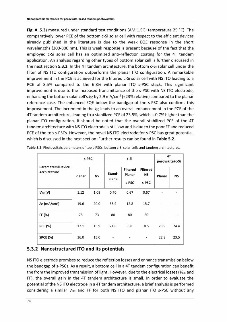
Nanophotonic electrodes for perovskite-based tandem photovoltaics
74
Fig. A. 5.3) measured under standard test conditions (AM 1.5G, temperature 25 °C). The
comparatively lower PCE of the bottom c-Si solar cell with respect to the efficient devices
already published in the literature is due to the weak EQE response in the short
wavelengths (300-800 nm). This is weak response is present because of the fact that the
employed c-Si solar cell has an optimized anti-reflection coating for the 4T tandem
application. An analysis regarding other types of bottom solar cell is further discussed in
the next section 5.3.2. In the 4T tandem architecture, the bottom c-Si solar cell under the
filter of NS ITO configuration outperforms the planar ITO configuration. A remarkable
improvement in the PCE is achieved for the filtered c-Si solar cell with NS ITO leading to a
PCE of 8.5% compared to the 6.8% with planar ITO s-PSC stack. This significant
improvement is due to the increased transmittance of the s-PSC with NS ITO electrode,
enhancing the bottom solar cell’s JSC by 2.9 mA/cm2 (≈23% relative) compared to the planar
reference case. The enhanced EQE below the bandgap of the s-PSC also confirms this
improvement. The increment in the JSC leads to an overall enhancement in the PCE of the
4T tandem architecture, leading to a stabilized PCE of 23.5%, which is 0.7% higher than the
planar ITO configuration. It should be noted that the overall stabilized PCE of the 4T
tandem architecture with NS ITO electrode is still low and is due to the poor FF and reduced
PCE of the top s-PSCs. However, the novel NS ITO electrode for s-PSC has great potential,
which is discussed in the next section. Further results can be found in Table 5.2.
Table 5.2: Photovoltaic parameters of top s-PSCs, bottom c-Si solar cells and tandem architectures.
Parameters/Device
Architecture
s-PSC c-Si 4T
perovskite/c-Si
Planar NS Stand-
alone
Filtered
Planar
s-PSC
Filtered
NS
s-PSC
Planar NS
VOC (V) 1.12 1.08 0.70 0.67 0.67 - -
JSC (mA/cm2) 19.6 20.0 38.9 12.8 15.7 - -
FF (%) 78 73 80 80 80 - -
PCE (%) 17.1 15.9 21.8 6.8 8.5 23.9 24.4
SPCE (%) 16.0 15.0 - - - 22.8 23.5
5.3.2 Nanostructured ITO and its potentials
NS ITO electrode promises to reduce the reflection losses and enhance transmission below
the bandgap of s-PSCs. As a result, a bottom cell in a 4T tandem configuration can benefit
the from the improved transmission of light. However, due to the electrical losses (VOC and
FF), the overall gain in the 4T tandem architecture is small. In order to evaluate the
potential of the NS ITO electrode in a 4T tandem architecture, a brief analysis is performed
considering a similar VOC and FF for both NS ITO and planar ITO s-PSC without any

Nanophotonic electrodes for perovskite-based tandem photovoltaics
75
hysteresis and assuming state-of-the-art c-Si solar cell with an enhanced EQE (labelled as
Cell A)182 and a CIGS solar cell (labelled as Cell B)183 as the bottom cells. Therefore, the PCEs
of the top s-PSCs with NS ITO electrode and planar ITO electrode are considered as 17.4%
and 17.1%, respectively. In the case of the state-of-the-art bottom cells, the bottom solar
cell’s EQE is derived by weighting the transmittance of the respective top cell with the EQE
of the stand-alone bottom solar cell. Cell A has a reported PCE of 26.1% and depicts an
enhanced EQE (compare Fig. 5.11b and Fig. 5.14a) for the entire wavelength range
300-1200 nm. Due to the enhancement of the EQE response, especially below the bandgap
of the top s-PSC, an improved PCE of 9.5% is obtained. The potential PCE of the 4T tandem
Fig. 5.13: (a) Time-resolved photoluminescence of perovskite absorber on planar and
nanostructured (NS) ITO electrodes. (b) Current density-voltage characteristics in
backward and forward scan directions and (c) stabilized power conversion efficiency
(PCE) of semitransparent perovskite solar cells (s-PSCs) fabricated with
nanostructured (NS) and planar ITO electrode. Adapted with permission from
reference [71], © 2020 Optical Society of America.

Nanophotonic electrodes for perovskite-based tandem photovoltaics
76
architecture is 27.0%, which is 1.1% higher than the c-Si solar cell used in this study. In the
case of the planar ITO electrode stack, the potential PCE calculated is only 24.9% and is
significantly smaller even than the stand-alone PCE of Cell A. In the case of Cell B in the 4T
tandem configuration, which represents an all thin film tandem architecture, the potential
PCE is reduced to 25.2% and is mostly due to the high bandgap and the weak EQE response
of the CIGS.
Table 5.3: Photovoltaic parameters: JSC and PCE of top s-PSCs, bottom c-Si solar cells and tandem
architectures.
Stack
JSC (mA/cm2) Potential PCE (%)
Stand-
alone
Filtered
Planar
s-PSC
Filtered
NS
s-PSC
Stand-
alone
Filtered
Planar
s-PSC
Filtered
NS
s-PSC
4T
Planar
4T
NS
Top planar 19.6 - - 17.1a - - - -
Top NS 20.0 - - 17.4a 12.8 - - -
Bottom c-Si
(this work) 38.9 12.8 15.7 21.8 6.8 8.5 23.9d 25.9e
Bottom Cell
A (c-Si [182]) 42.6 13.2f 16.4 26.1 7.8b 9.6b 24.9d 27.0e
Bottom Cell
B (CIGS [183]) 35.9 11.2f 13.7 21.7 6.4c 7.8c 23.5d 25.2e
Fig. 5.14: External quantum efficiency (EQE) of c-Si solar cell adapted from [182], referred as Cell A and CIGS solar cell adapted from [183], referred as Cell B. The EQE of the devices are also presented in stand-alone or four-terminal tandem configuration under filters of semitransparent perovskite solar cells fabricated with planar or nanostructured ITO. Adapted with permission from reference [71], © 2020 Optical Society of America.

Nanophotonic electrodes for perovskite-based tandem photovoltaics
77
aThe PCE of the top s-PSCs are estimated considering same VOC, FF and no hysteresis for both planar and NS
ITO based devices. The following parameters are considered to calculate the PCE: bCell A: FF – 0.843; VOC –
0.697 V, cCell B: FF – 0.793; VOC – 0.716 V. dSum of PCEs of top planar device and bottom cell. eSum of PCEs
of top NS device and bottom cell. fBy weighting the EQE of the stand-alone cell with the transmission of the
respective filter, the JSC is obtained.
Thus, two critical requirements of a 4T tandem architecture can be derived from this
analysis: (i) in order to maximize the overall PCE, a bottom solar cell with enhanced EQE
response below the bandgap of the top PSC should be considered, and (ii) a high
transmission of the top cell is required (obtained with NS ITO electrode here) so that the
PCE of the tandem architecture is higher than the stand-alone PCE of the sub-cells. In
summary, the NS ITO based tandem solar cells shows the potential to improve the PCE
significantly compared to it planar counterparts. Further information can be found in Table
5.3.
5.3.3 Energy yield analysis for perovskite solar cells with NS ITO
Nanostructured ITO are more robust in terms of angular selectivity, therefore, the
dependence on the angles of incidence (AOI)180 of the light is reduced. Therefore, this
feature of reduced angular selectivity with nanostructures is very interesting for solar
energy harvesting applications as the power generated by solar cells is highly dependent
on the AOI of light, which changes throughout the day. To investigate this for the 4T
perovskite/c-Si tandem architecture, the specular transmittance of the s-PSCs with NS ITO
electrode and planar ITO electrode are compared for various AOI. For oblique angles, the
specular transmittance with the NS ITO electrode drops only slightly, while a significant
reduction in the transmittance is observed for the planar ITO case (Fig. 5.15).
To obtain more insights EQE measurements are performed on each the sub-cells and the
JSC is determined (Fig. 5.16). Table 5.4 summarizes the obtained JSC. It is evident that up to
Fig. 5.15: Specular transmittance (T) of semitransparent perovskite solar cells with (a) planar ITO and (b) NS ITO for various angles of incidence. For oblique angles, the specular transmittance with the NS ITO electrode drops only slightly, while a significant reduction in the transmittance is observed for the planar ITO stack. Adapted with permission from reference [71], © 2020 Optical Society of America.
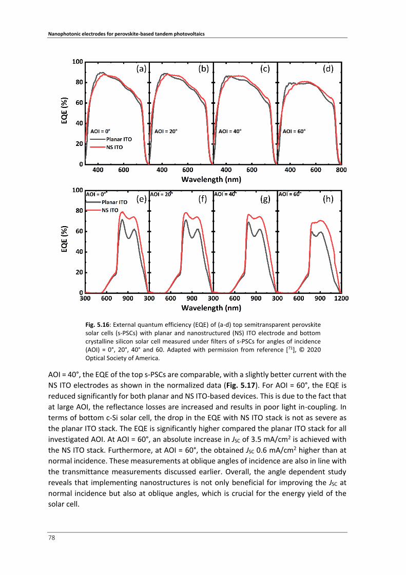
Nanophotonic electrodes for perovskite-based tandem photovoltaics
78
AOI = 40°, the EQE of the top s-PSCs are comparable, with a slightly better current with the
NS ITO electrodes as shown in the normalized data (Fig. 5.17). For AOI = 60°, the EQE is
reduced significantly for both planar and NS ITO-based devices. This is due to the fact that
at large AOI, the reflectance losses are increased and results in poor light in-coupling. In
terms of bottom c-Si solar cell, the drop in the EQE with NS ITO stack is not as severe as
the planar ITO stack. The EQE is significantly higher compared the planar ITO stack for all
investigated AOI. At AOI = 60°, an absolute increase in JSC of 3.5 mA/cm2 is achieved with
the NS ITO stack. Furthermore, at AOI = 60°, the obtained JSC 0.6 mA/cm2 higher than at
normal incidence. These measurements at oblique angles of incidence are also in line with
the transmittance measurements discussed earlier. Overall, the angle dependent study
reveals that implementing nanostructures is not only beneficial for improving the JSC at
normal incidence but also at oblique angles, which is crucial for the energy yield of the
solar cell.
Fig. 5.16: External quantum efficiency (EQE) of (a-d) top semitransparent perovskite solar cells (s-PSCs) with planar and nanostructured (NS) ITO electrode and bottom crystalline silicon solar cell measured under filters of s-PSCs for angles of incidence (AOI) = 0°, 20°, 40° and 60. Adapted with permission from reference [71], © 2020 Optical Society of America.
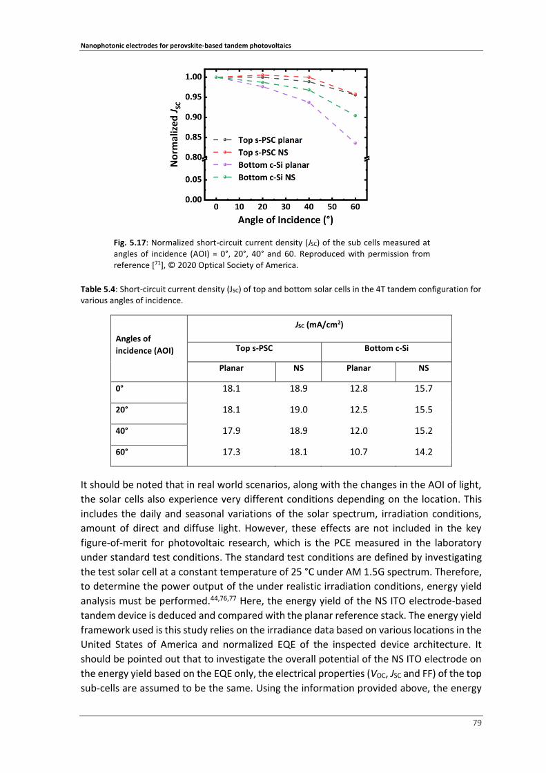
Nanophotonic electrodes for perovskite-based tandem photovoltaics
79
Table 5.4: Short-circuit current density (JSC) of top and bottom solar cells in the 4T tandem configuration for various angles of incidence.
Angles of
incidence (AOI)
JSC (mA/cm2)
Top s-PSC Bottom c-Si
Planar NS Planar NS
0° 18.1 18.9 12.8 15.7
20° 18.1 19.0 12.5 15.5
40° 17.9 18.9 12.0 15.2
60° 17.3 18.1 10.7 14.2
It should be noted that in real world scenarios, along with the changes in the AOI of light,
the solar cells also experience very different conditions depending on the location. This
includes the daily and seasonal variations of the solar spectrum, irradiation conditions,
amount of direct and diffuse light. However, these effects are not included in the key
figure-of-merit for photovoltaic research, which is the PCE measured in the laboratory
under standard test conditions. The standard test conditions are defined by investigating
the test solar cell at a constant temperature of 25 °C under AM 1.5G spectrum. Therefore,
to determine the power output of the under realistic irradiation conditions, energy yield
analysis must be performed.44,76,77 Here, the energy yield of the NS ITO electrode-based
tandem device is deduced and compared with the planar reference stack. The energy yield
framework used is this study relies on the irradiance data based on various locations in the
United States of America and normalized EQE of the inspected device architecture. It
should be pointed out that to investigate the overall potential of the NS ITO electrode on
the energy yield based on the EQE only, the electrical properties (VOC, JSC and FF) of the top
sub-cells are assumed to be the same. Using the information provided above, the energy
Fig. 5.17: Normalized short-circuit current density (JSC) of the sub cells measured at angles of incidence (AOI) = 0°, 20°, 40° and 60. Reproduced with permission from reference [71], © 2020 Optical Society of America.
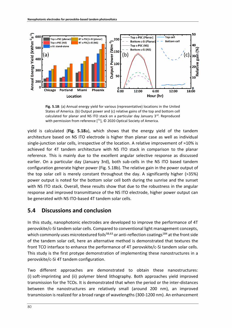
Nanophotonic electrodes for perovskite-based tandem photovoltaics
80
yield is calculated (Fig. 5.18a), which shows that the energy yield of the tandem
architecture based on NS ITO electrode is higher than planar case as well as individual
single-junction solar cells, irrespective of the location. A relative improvement of ≈10% is
achieved for 4T tandem architecture with NS ITO stack in comparison to the planar
reference. This is mainly due to the excellent angular selective response as discussed
earlier. On a particular day (January 3rd), both sub-cells in the NS ITO based tandem
configuration generate higher power (Fig. 5.18b). The relative gain in the power output of
the top solar cell is merely constant throughout the day. A significantly higher (>35%)
power output is noted for the bottom solar cell both during the sunrise and the sunset
with NS ITO stack. Overall, these results show that due to the robustness in the angular
response and improved transmittance of the NS ITO electrode, higher power output can
be generated with NS ITO-based 4T tandem solar cells.
5.4 Discussions and conclusion
In this study, nanophotonic electrodes are developed to improve the performance of 4T
perovskite/c-Si tandem solar cells. Compared to conventional light management concepts,
which commonly uses microtextured foils58,63 or anti-reflection coatings184 at the front side
of the tandem solar cell, here an alternative method is demonstrated that textures the
front TCO interface to enhance the performance of 4T perovskite/c-Si tandem solar cells.
This study is the first protype demonstration of implementing these nanostructures in a
perovskite/c-Si 4T tandem configuration.
Two different approaches are demonstrated to obtain these nanostructures:
(i) soft-imprinting and (ii) polymer blend lithography. Both approaches yield improved
transmission for the TCOs. It is demonstrated that when the period or the inter-distances
between the nanostructures are relatively small (around 200 nm), an improved
transmission is realized for a broad range of wavelengths (300-1200 nm). An enhancement
Fig. 5.18: (a) Annual energy yield for various (representative) locations in the United States of America. (b) Output power and (c) relative gains of the top and bottom cell calculated for planar and NS ITO stack on a particular day January 3rd. Reproduced with permission from reference [71], © 2020 Optical Society of America.
Nanophotonic electrodes for perovskite-based tandem photovoltaics
81
of ≈5% and ≈7% is observed for periodic ITO and disordered nanostructured ITO,
respectively. The broad range of improvement is particularly interesting for tandem solar
cells as this leads to enhanced short-circuit current densities for both the sub cells in the
tandem configuration. These results are also consistent with existing simulation and
experimental results that were already demonstrated in the literature.72 The improved
transmission is attributed to a gradual matching of the refractive index that reduces the
overall reflection losses. One particular challenge that still needs to be overcome is the
formation of cracks between the nanostructures in the NS ITO. These cracks impede the
charge carriers transfer and as a result, an increase in the sheet resistance is observed
these TCOs. However, further optimization of the sputtering condition can be employed in
future studies to avoid the formation of these cracks.
The reduced reflections with the NS ITO lead to an improved JSC in both top s-PSCs and
bottom c-Si solar cells. While for the top s-PSCs, the increase is around ≈3% relative, a
significant improvement in the short-circuit current density for the bottom solar cell
(≈23% relative) is observed. This improvement in the top s-PSC is comparable to a recently
published work, where similar NS TCOs fabricated from nanopillars were employed, but
for opaque PSC.185 The sum of short-circuit current densities by both the sub cells is ≈10%
relative higher with the nanostructured ITO stack compared to the planar. This exceeds
the enhancement observed previously by Jaysankar et al. (3.2% relative) in 4T
perovskite/c-Si tandem modules, which incorporated an inverted pyramidal micro-texture
at the air/glass interface.38 This shows that reducing the optical losses at the front TCO
interface is also important in improving the JSC in tandem solar cells. Although there is an
improvement in the short-circuit current densities, top s-PSCs suffer from enhanced
recombination losses. As a result, s-PSCs yielded reduced VOC and PCE. In a recent study,
Tochhorn et al. already demonstrated that this voltage loss can be overcome by utilizing
self-assembled monolayers that conformally covers the nanostructured TCOs.185 Overall,
for the tandem architecture with NS ITO, an improved PCE of 0.7% is achieved. Further
analysis reveals a potential increase in the PCE by 2.1% for the NS ITO stack if similar
performance of the top s-PSCs is achieved by both planar and NS ITO electrode. Moreover,
angle dependent transmittance and EQE measurements show that devices based on NS
ITO electrode are more robust and have better angular stability compared to planar stacks.
To verify this, angular dependent analysis is extended to energy yield calculations. The
results reveal that NS ITO based devices improve the annual output power by a
relative ≈10% independent of locations compared to the planar ITO electrode. Thus, it is
highly important to overcome the remaining challenges associated with the NS ITO and
fully exploit the potentials in perovskite-based tandem architectures.

Nanophotonic electrodes for perovskite-based tandem photovoltaics
82

83
6. Semitransparent perovskite solar cells for four-
terminal tandem architectures
This chapter discusses semitransparent perovskite solar cells for four-terminal
perovskite/c-Si and perovskite/CIGS tandem architectures. The first part of this chapter
deals with research question 3 and discusses engineering of the bandgap of the perovskite
absorber layer to determine the optimum for maximizing power conversion efficiency in a
four-terminal tandem architecture. A detailed study of the various properties of the
absorber layer is also presented. The second part of this chapter deals with research
question 2 and investigates both transparent conductive oxide electrodes present in
semitransparent perovskite solar cells to determine the optical loss channels that reduce
the power conversion efficiency in the four-terminal tandem architecture. Furthermore,
alternative materials are proposed that demonstrate improved overall power conversion
efficiency for the perovskite-based four-terminal tandem architecture.
Acknowledgements and contributions
The first part of this chapter on semitransparent perovskite solar cells for four-terminal
tandem architectures with engineered bandgap is already published in reference [99]. This
publication is a collaboration between KIT, ISFH and ZSW. The research article is an equally-
shared work between Ihteaz M. Hossain and Saba Gharibzadeh. In this collaboration,
Ihteaz M. Hossain contributed the fabrication of the semitransparent perovskite solar cells
and characterizations related to the four-terminal architecture. The second part of this
chapter discusses the transparent conductive oxide electrodes for semitransparent
perovskite solar cells. Part of the second chapter is already submitted in reference [186] for
publication. Ihteaz M. Hossain acknowledges the support of Saba Gharibzadeh, Isabel
Allegro, David Ritzer, Adrian Mertens and Michael Hetterich in various experimental
procedures. Ihteaz M. Hossain also acknowledges the support of Mortiz Schultes and Erik
Ahlswede of Zentrum für Sonnenenergie und Wasserstoff-Forschung Baden-Württemberg
(ZSW) for providing samples and discussions. Finally, Ihteaz M. Hossain acknowledges

Semitransparent perovskite solar cells for four-terminal tandem architectures
84
various fruitful discussion with Somayeh Moghadamzadeh, Paul Fassl, Yidenekachew Donie
and Raphael Schmager during the course of this study.

Semitransparent perovskite solar cells for four-terminal tandem architectures
85
A critical requirement in a tandem solar cell architecture is to find the optimum bandgaps
and the materials for the top and bottom solar cells as discussed in chapter 2, section 2.4.
To date, the choice of the bottom solar cell has been straight forward since the bandgap
of the established technologies in photovoltaic industry is ≈1.0 eV: crystalline-silicon (c-Si)
has a bandgap of ≈1.1 eV and copper indium gallium selenide’s (CIGS) bandgap can be
varied between 1.0-1.2 eV. Next to the already established technologies, low-bandgap
perovskite solar cells (PSCs) are another viable option as the bandgap can be tuned from
1.1-1.3 eV by the partial substitution of Pb2+ with Sn2+ and furthermore, it would allow for
all solution-processed, low-cost tandem photovoltaics.82 In terms of the top solar cell,
wide-bandgap PSCs are interesting candidates as the bandgap of the absorber can be
tuned between 1.5-2.3 eV by varying the stoichiometry of the material.84,98
Due to ease in the current matching condition in the four-terminal (4T) tandem
architecture, a wide range of bandgaps (1.60-1.85 eV) for the top perovskite absorber can
demonstrate very high PCE with the optimum at 1.81 eV as shown in simulations.17,18 The
current record 4T perovskite/c-Si tandem device (28.2%) uses a bandgap of 1.63 eV
(extracted from external quantum efficiency measurement),14 whereas a bandgap of
1.68 eV was demonstrated to be the optimum for 4T perovskite/CIGS tandem solar cells
(25.9%).45 Both of these studies use significantly smaller bandgaps than the optimum for
the top perovskite absorber in tandem configurations as demonstrated in simulations,
which raises the question of the optimum bandgap of the top absorber in perovskite-based
tandem PV for real prototype devices.
One of the reasons for this difference is the non-radiative recombination losses and
imperfect contact properties of the wide bandgap PSCs that affect the device performance,
and result in a large open-circuit voltage (VOC) deficit (defined by Eg/q-VOC).25,38,169,170 Wide
bandgap perovskite absorber conventionally uses a bromine-rich stoichiometry to increase
the bandgap.25,34,58,63,80,98,187 In such compositions, recombination loss mechanism are
dominated by photo-induced phase segregation and subsequent funneling of charge
carriers into iodide-rich lower bandgap regions.19 Furthermore, these wide bandgap
materials present a higher number of deep defect states20,21,188 and a stronger interfacial
recombination in full devices,22–24 all of which result in a strong VOC deficit.25–27,189 It was
recently demonstrated by our research group that a 2D Ruddlesden–Popper (2D-RP)
structure can passivate the bulk perovskite absorber and reduce the VOC deficit.13,91 The
2D passivation is obtained by depositing a thin layer of n‐butylammonium bromide
(n-BABr) on the perovskite absorber, forming a 2D/3D heterostructure that passivates the
surface defects and demonstrates an improvement in the lifetime of the charge carriers.
Thus, the 2D/3D heterostructure mitigates non-radiative recombination losses and PSCs
fabricated with these heterostructures demonstrated an enhanced VOC (≈80 mV)
compared to the reference bulk 3D absorber.91
Next to the recombination losses that affect the electrical properties, optical losses such
as reflections at interfaces and parasitic absorption within the layer stack reduce the
transmission of the top solar cell and decreases the overall PCE in the tandem
architecture.15,16,71,190 One of the main sources of these optical losses are the transparent

Semitransparent perovskite solar cells for four-terminal tandem architectures
86
conductive oxide (TCO) electrodes as discussed in chapter 2, section 2.5 and thoroughly in
chapter 5. Fluorine-doped tin oxide (FTO) is a commonly employed front TCO for opaque
PSCs, however it shows strong parasitic absorption losses both in the visible and near
infrared wavelengths (see also Appendix Fig. A. 4.1),36,191 and is thus not feasible for
perovskite-based tandem applications. Another widely used front TCO is tin-doped indium
oxide (ITO), which shows significantly reduced absorption losses compared to FTO,
however, the absorption and reflection losses in the near infrared wavelengths due to the
free charge carriers39,192 may still limit the overall PCE for tandem devices. Therefore,
further work must be carried out to improve the optical properties of ITO to make it more
suitable for tandems applications or alternate materials must be investigated to replace it.
In the literature, several material with improved electrical properties and low optical losses
already exist that promise to replace ITO, for example zinc-doped indium oxide (IZO),
hydrogenated indium oxide (IO:H) and others.36,58,80
In the first part of this chapter, the aspect of the optimum bandgap of the perovskite
absorber in a 4T tandem architecture is experimentally investigated. For this, PSCs with
engineered bandgaps are fabricated and a 2D/3D heterostructure is incorporated to
reduce the VOC deficit. Semitransparent perovskite solar cells (s-PSCs) are mechanically-
stacked with c-Si and CIGS bottom solar cells to determine the optimum bandgap for the
4T perovskite/c-Si and perovskite/CIGS multi-junction solar cells. In the second part of the
chapter, a detailed investigation on the optical properties of different TCOs is carried out
to identify the optical loss mechanisms in a 4T perovskite/c-Si tandem architecture. Finally,
s-PSCs with TCO electrodes with improved optical properties are fabricated to enhance the
PCE in perovskite/c-Si tandem solar cells.
6.1 Bandgap tuning of perovskite absorbers
In this section, the influence of the bandgap of the top wide-bandgap perovskite absorber
on the performance of 4T-tandem perovskite-based tandems is investigated in detail.
Initially, the material properties of perovskite films with various bandgaps are studied,
followed by the fabrication of opaque perovskite solar cells (o-PSCs) and s-PSCs. Finally,
Fig. 6.1: (a) Absorbance spectra and (b) Tauc plots of the spin-coated layers with
bandgaps 1.65 eV, 1.69 eV, 1.74 eV, 1,79 eV and 1.85 eV for the 2D/3D perovskite
heterostructure. Adapted with permission from reference [99], © John Wiley & Sons.

Semitransparent perovskite solar cells for four-terminal tandem architectures
87
s-PSCs are mechanically-stacked on top of bottom c-Si and CIGS solar cells to study the
device performance of the 4T tandem architecture.
6.1.1 Material properties
Five different bandgaps of double cation perovskite absorbers (FA0.83Cs0.17Pb(I1−yBry)3)
based on formamidinium (FA) and cesium (Cs) are investigated to determine the optimum
bandgap of the top PSC in a 4T tandem architecture. In order to vary the bandgap, the
content of bromine (0.24 ≤ y ≤ 0.56) in the precursor solution is varied in steps of Δy = 0.08.
Furthermore, a 2D/3D perovskite heterostructure is obtained for each of these bandgaps
by spin coating n-butylammonium bromide (n-BABr) dissolved in isopropanol on top of the
3D perovskite absorber. The absorptance spectra obtained from spectrophotometric
measurements show a shift towards lower wavelengths for increased bromine content
(Fig. 6.1a), demonstrating the widening of the bandgap. The bandgaps of the perovskite
absorbers are determined using Equation 4.1 and considering a direct optical transition
(Fig. 6.1b). A wide range of bandgaps of the perovskite absorber are formed (1.65-1.85 eV),
which, according to the simulations17,75 are in the optimum range to obtain an efficient 4T
tandem device. It should be noted that the determination of the bandgaps here might also
be affected by the excitonic absorption, which is more pronounced for higher bromide
concentrations as observed from the appearance in the excitonic nature of the absorbance
spectra. This is why Tauc plot is not the ideal method for the determination of the bandgap.
A more accurate estimation of the bandgap would be to use an Elliot fit and obtaining the
bandgap from the fitted excitonic continuum.193 However, for this study, the relative
differences in the bandgaps are more important. As a result, the simpler Tauc plot method
is employed that is most commonly followed in the literature for perovskite absorbers
even though there are various other ways to determine the bandgap.194
In order to determine the presence of the 2D structure, x-ray diffraction (XRD)
measurements are carried out on these different bandgaps. The results reveal weak but
Fig. 6.2: X-ray diffraction (XRD) pattern of the spin-coated layers with bandgaps 1.65 eV, 1.69 eV, 1.74 eV, 1,79 eV and 1.85 eV for the 2D/3D perovskite heterostructure. Adapted with permission from reference [99], © John Wiley & Sons.
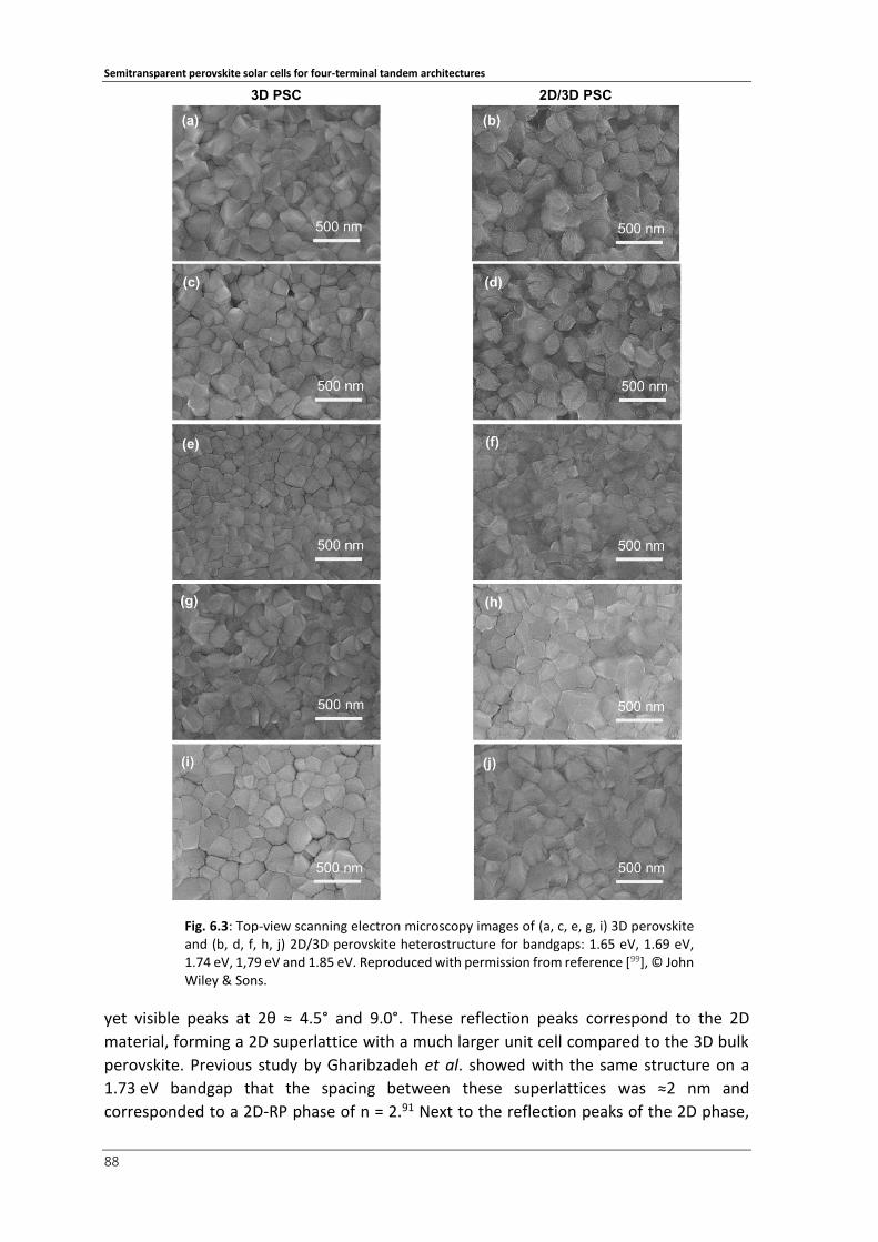
Semitransparent perovskite solar cells for four-terminal tandem architectures
88
yet visible peaks at 2θ ≈ 4.5° and 9.0°. These reflection peaks correspond to the 2D
material, forming a 2D superlattice with a much larger unit cell compared to the 3D bulk
perovskite. Previous study by Gharibzadeh et al. showed with the same structure on a
1.73 eV bandgap that the spacing between these superlattices was ≈2 nm and
corresponded to a 2D-RP phase of n = 2.91 Next to the reflection peaks of the 2D phase,
Fig. 6.3: Top-view scanning electron microscopy images of (a, c, e, g, i) 3D perovskite and (b, d, f, h, j) 2D/3D perovskite heterostructure for bandgaps: 1.65 eV, 1.69 eV, 1.74 eV, 1,79 eV and 1.85 eV. Reproduced with permission from reference [99], © John Wiley & Sons.

Semitransparent perovskite solar cells for four-terminal tandem architectures
89
the XRD measurements show the typical bulk 3D perovskite reflection peaks from the
planes (100), (110), (111) and (200). With the increase in bromine concentration, a
consistent shift of the reflection peaks towards higher angles are observed. This can be
attributed to the increased lattice contraction due to the decrease in the perovskite crystal
structure as smaller bromide ions now replace the larger iodide ions.195 To observe any
morphological changes due to the presence of the 2D phase on the bulk 3D perovskite,
scanning electron microscopy (SEM) is performed on these samples. The images reveal a
minor modification of the surface texture of the films with 2D/3D heterostructure for all
bandgaps compared to the bulk 3D reference (Fig. 6.3). Thus, it indicates that the 2D layer
forms a very thin layer on the surface of the 3D bulk, which is in consistent with the
previous studies of Gharibzadeh et al. and Doung et al.13,91 In the next section, the
performance of the PSCs with 2D/3D heterostructure for various bandgaps is investigated.
6.1.2 Photovoltaic characteristics of perovskite solar cells for optimum
bandgap
o-PSCs are fabricated to investigate the effect of the 2D/3D heterostructure on the
photovoltaic parameters. The device layer stack is comprised of glass/ITO/ np-SnO2/
(2D/3D perovskite or 3D perovskite)/spiro‐MeOTAD/Au (Fig. 6.4a). An in-house sputtered
ITO (ITOv, see chapter 3, section 3.1.3 for more information about the deposition) is used.
The open-circuit voltages of the champion devices are shown in Fig. 6.4b. An enhancement
of ≈45 mV in the VOC is observed for all investigated bandgaps using the 2D/3D
heterostructure, which can be attributed to the reduction in the non-radiative
recombination losses as discussed by Gharibzadeh et al. and Doung et al.13,91 They show
an increase in the lifetime of the charge carriers for 2D/3D perovskite heterostructure
compared to the bulk 3D perovskite. Furthermore, a better energetic alignment with the
hole transport layer may also result in the overall improvement of the VOC.196 Fig. 6.4b also
shows that the VOC increases linearly with increasing bandgap from 1.65-1.74 eV,
independent of the 2D passivation layer. Up on a further increase of the bandgap to
1.85 eV, the VOC reaches a maximum and subsequently decreases. An enhanced VOC deficit
Fig. 6.4: (a) Schematic of the perovskite solar cell (PSC) with 2D/3D perovskite heterostructure. (b) Open-circuit voltage (VOC) as a function of the bandgap of the perovskite absorbers for opaque PSCs. Adapted with permission from reference [99], © John Wiley & Sons.

Semitransparent perovskite solar cells for four-terminal tandem architectures
90
is a commonly observed phenomenon for PSCs with high bromine content and is attributed
to increased recombination losses as discussed earlier.19–27,188,189 In order to compare the
obtained VOC for all the different bandgaps with existing literature, a literature survey of
reported champion open‐circuit voltages is shown in Appendix, Fig. A.6.1. The results
show that, the 2D passivated PSCs in this study yield high open‐circuit voltages over a
broad range of bandgaps and are among the highest reported in the literature.
Furthermore, to the best of our knowledge, it is the first time an effective 2D passivation
approach is reported over such a broad range of bandgaps. More detailed information
regarding derivation of the bandgaps from external quantum efficiency (EQE)
measurement as well as a table of the VOC and the VOC deficit values can be found in the
Appendix, Table A. 6.1. It should be noted that the VOC of the presented devices here is
≈30 mV lower than in the previous work by Gharibzadeh et al. for the same layer stack as
Fig. 6.5: Current density-voltage (J-V) characteristics of opaque perovskite solar cells fabricated with (a) 3D perovskite and (b) 2D/3D perovskite heterostructure for bandgaps: 1.65 eV, 1.69 eV, 1.74 eV, 1,79 eV and 1.85 eV.
Fig. 6.6: Power conversion efficiency (PCE) derived from (a) current density-voltage characteristics and (b) measuring at a constant voltage near the maximum power point for the various bandgaps of perovskite absorber. Adapted with permission from reference [99], © John Wiley & Sons.

Semitransparent perovskite solar cells for four-terminal tandem architectures
91
shown in Fig. 6.4c.91 The probable reason could be the poorer quality of the precursor
material PbI2 from the supplier during the course of this study, which is the key component
in fabricating highly efficient PSCs (see Notes at:
https://www.tcichemicals.com/eshop/en/us/commodity/L0279/).
Next to the VOC, the fill factor (FF) of the 2D/3D o-PSCs shows an improvement of 1.5-2%
absolute compared to the 3D bulk devices (Table 6.1 and Fig. 6.5). The short-circuit current
density (JSC) derived from the current density-voltage (J-V) characteristic shows a similar
reduction with increasing bandgap for both 3D and 2D/3D samples. This is an indication
that the thickness of the perovskite absorber is not significantly modified by the addition
Fig. 6.7: (a) Cross-section scanning electron microscopy image of a semitransparent perovskite solar cell (s-PSC) with 2D/3D perovskite heterostructure. (b-f) Current density-voltage (J-V) characteristics of the s-PSCs for bandgaps: 1.65 eV, 1.69 eV, 1.74 eV, 1,79 eV and 1.85 eV. Adapted with permission from reference [99], © John Wiley & Sons.
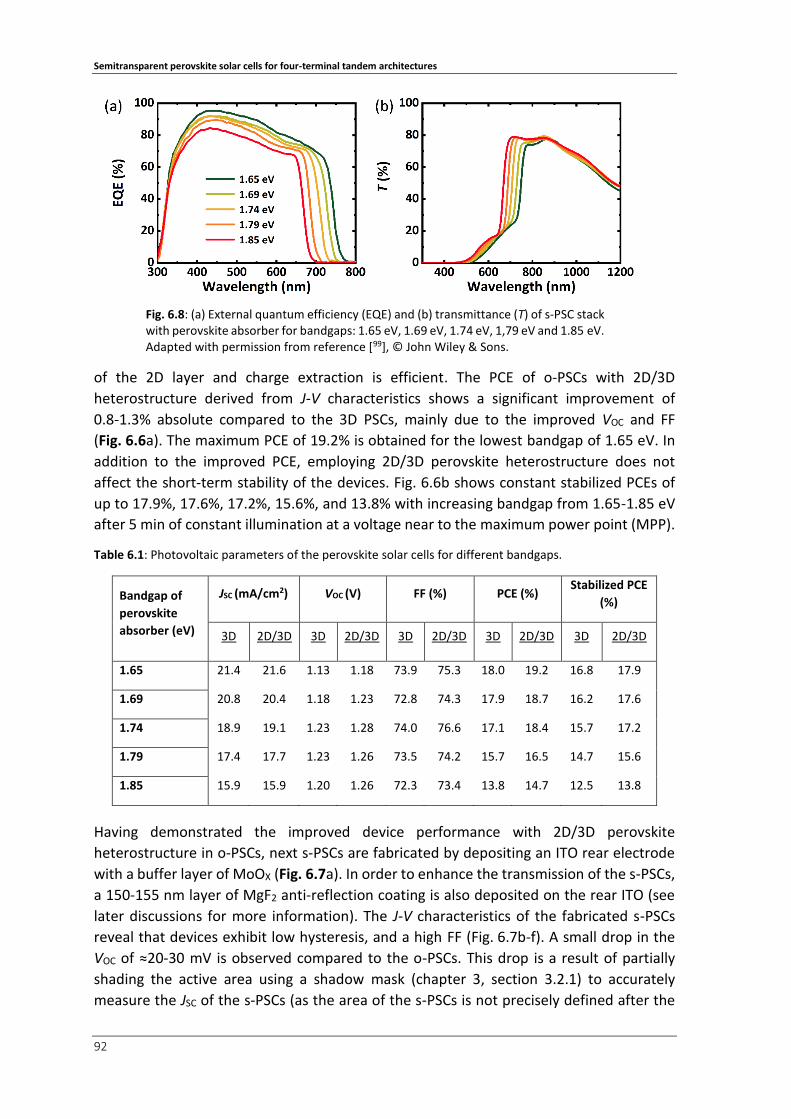
Semitransparent perovskite solar cells for four-terminal tandem architectures
92
of the 2D layer and charge extraction is efficient. The PCE of o-PSCs with 2D/3D
heterostructure derived from J-V characteristics shows a significant improvement of
0.8-1.3% absolute compared to the 3D PSCs, mainly due to the improved VOC and FF
(Fig. 6.6a). The maximum PCE of 19.2% is obtained for the lowest bandgap of 1.65 eV. In
addition to the improved PCE, employing 2D/3D perovskite heterostructure does not
affect the short-term stability of the devices. Fig. 6.6b shows constant stabilized PCEs of
up to 17.9%, 17.6%, 17.2%, 15.6%, and 13.8% with increasing bandgap from 1.65-1.85 eV
after 5 min of constant illumination at a voltage near to the maximum power point (MPP).
Table 6.1: Photovoltaic parameters of the perovskite solar cells for different bandgaps.
Bandgap of
perovskite
absorber (eV)
JSC (mA/cm2) VOC (V) FF (%) PCE (%) Stabilized PCE
(%)
3D 2D/3D 3D 2D/3D 3D 2D/3D 3D 2D/3D 3D 2D/3D
1.65 21.4 21.6 1.13 1.18 73.9 75.3 18.0 19.2 16.8 17.9
1.69 20.8 20.4 1.18 1.23 72.8 74.3 17.9 18.7 16.2 17.6
1.74 18.9 19.1 1.23 1.28 74.0 76.6 17.1 18.4 15.7 17.2
1.79 17.4 17.7 1.23 1.26 73.5 74.2 15.7 16.5 14.7 15.6
1.85 15.9 15.9 1.20 1.26 72.3 73.4 13.8 14.7 12.5 13.8
Having demonstrated the improved device performance with 2D/3D perovskite
heterostructure in o-PSCs, next s-PSCs are fabricated by depositing an ITO rear electrode
with a buffer layer of MoOX (Fig. 6.7a). In order to enhance the transmission of the s-PSCs,
a 150-155 nm layer of MgF2 anti-reflection coating is also deposited on the rear ITO (see
later discussions for more information). The J-V characteristics of the fabricated s-PSCs
reveal that devices exhibit low hysteresis, and a high FF (Fig. 6.7b-f). A small drop in the
VOC of ≈20-30 mV is observed compared to the o-PSCs. This drop is a result of partially
shading the active area using a shadow mask (chapter 3, section 3.2.1) to accurately
measure the JSC of the s-PSCs (as the area of the s-PSCs is not precisely defined after the
Fig. 6.8: (a) External quantum efficiency (EQE) and (b) transmittance (T) of s-PSC stack with perovskite absorber for bandgaps: 1.65 eV, 1.69 eV, 1.74 eV, 1,79 eV and 1.85 eV. Adapted with permission from reference [99], © John Wiley & Sons.

Semitransparent perovskite solar cells for four-terminal tandem architectures
93
sputtering of ITO). Therefore, a dark solar cell, which is in forward bias, is formed in parallel
with the solar cell under light, leading to a reduction in the VOC. Furthermore, as the
fabricated PSCs are semitransparent, the devices show 1-1.5 mA/cm2 lower JSC than the
o-PSCs, which is due to reduced optical path length, and poor reflection by the rear ITO.
EQE measurements conducted on these samples show that the EQE is reduced in the
wavelength range between 550-800 nm (Fig. 6.8a). In accordance with the absorbance
spectra in Fig. 6.1a for increasing bandgap, a consistent shift in the onset of the EQE signal
towards shorter wavelengths is also noted. Moreover, a reduced EQE is observed for
increasing bandgaps. This might be associated to a poorer charge extraction or an
Fig. 6.9: Stability of perovskite solar cells with 2D/3D heterostructure. (a) Power conversion efficiency (PCE) and (b) normalized PCE of semitransparent perovskite solar cells (s-PSCs) with bandgaps: 1.65 eV, 1.69 eV, 1.74 eV, 1,79 eV and 1.85 eV measured at constant voltages near the maximum power point. (c) Long term stability test of s-PSC for bandgap = 1.65 eV. Adapted with permission from reference [99], © John Wiley & Sons.

Semitransparent perovskite solar cells for four-terminal tandem architectures
94
enhanced carrier trapping in the bromine-rich absorber layers.22,23 Overall, a reduction in
the stabilized PCE is observed for the s-PSCs compared to the o-PSCs (Fig. 6.9a). The
stabilized PCE of the champion devices over a course of 5 minutes are 17.5%, 16.5%, 15.8%,
14.4%, and 12.1% for the bandgaps 1.65 eV, 1.69 eV, 1.74 eV, 1.79 eV and 1.85 eV,
respectively. In order to obtain more insights in the stability of the fabricated s-PSCs, the
effect of long-term exposures to constant light and bias on the devices is investigated. For
a 1-hour exposure of AM 1.5G irradiation at a constant voltage near the MPP, the s-PSCs
with bandgap up to 1.74 eV show no reduction in the normalized PCE (Fig. 6.9b). For
Eg = 1.79 eV and 1.85 eV, the s-PSCs remain stable for up to 30 mins and then reduces to
96% and 94% of its initial value after 1 hour, respectively. This demonstrates that although
the wider bandgap PSCs show short term stability (Fig. 6.10a), they are yet not stable for
longer times. Therefore, further investigation is required to improve the stability of PSCs
with bandgaps > 1.74 eV. For the Eg = 1.65 eV that depicted the highest PCE, the exposure
time is further increased to 11 hours, which shows high stability in the power output
(Fig. 6.9c). Further information regarding the statistical analysis of the various parameters
Fig. 6.10: Statistical analysis of the (a) short-circuit current density (JSC), (b) open-circuit voltage (VOC), (c) fill factor (FF) and (d) power conversion efficiency (PCE). Adapted with permission from reference [99], © John Wiley & Sons.
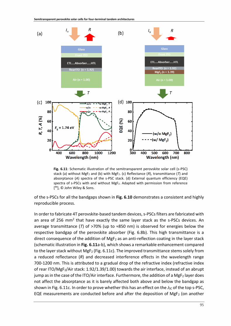
Semitransparent perovskite solar cells for four-terminal tandem architectures
95
of the s-PSCs for all the bandgaps shown in Fig. 6.10 demonstrates a consistent and highly
reproducible process.
In order to fabricate 4T perovskite-based tandem devices, s-PSCs filters are fabricated with
an area of 256 mm2 that have exactly the same layer stack as the s-PSCs devices. An
average transmittance (T) of >70% (up to ≈850 nm) is observed for energies below the
respective bandgap of the perovskite absorber (Fig. 6.8b). This high transmittance is a
direct consequence of the addition of MgF2 as an anti-reflection coating in the layer stack
(schematic illustration in Fig. 6.11a-b), which shows a remarkable enhancement compared
to the layer stack without MgF2 (Fig. 6.11c). The improved transmittance stems solely from
a reduced reflectance (R) and decreased interference effects in the wavelength range
700-1200 nm. This is attributed to a gradual drop of the refractive index (refractive index
of rear ITO/MgF2/Air stack: 1.92/1.39/1.00) towards the air interface, instead of an abrupt
jump as in the case of the ITO/Air interface. Furthermore, the addition of a MgF2 layer does
not affect the absorptance as it is barely affected both above and below the bandgap as
shown in Fig. 6.11c. In order to prove whether this has an effect on the JSC of the top s-PSC,
EQE measurements are conducted before and after the deposition of MgF2 (on another
Fig. 6.11: Schematic illustration of the semitransparent perovskite solar cell (s-PSC) stack (a) without MgF2 and (b) with MgF2. (c) Reflectance (R), transmittance (T) and absorptance (A) spectra of the s-PSC stack. (d) External quantum efficiency (EQE) spectra of s-PSCs with and without MgF2. Adapted with permission from reference [99], © John Wiley & Sons.

Semitransparent perovskite solar cells for four-terminal tandem architectures
96
set of devices). Insignificant differences are observed in the EQE spectra with the
integrated JSC differing by only 0.15 mA/cm2 (Fig. 6.11d).
In order to estimate the achievable 4T tandem solar cell PCE, the s-PSC filters are
mechanically-stacked on highly efficient interdigitated back contact (IBC) c‐Si (Eg ≈ 1.1 eV,
PCE = 23.2%) or CIGS (Eg = 1.13 eV, PCE = 21.2%) solar cells, forming perovskite/c-Si and
perovskite/CIGS tandem devices (schematic illustrations in Fig. 6.12a-b). For both c-Si solar
cell and CIGS solar cells, a quasi-linear increase in the filtered stabilized PCE in observed
(Fig. 6.12c). This is due to an increase in the photo-generated current as a higher number
of photons is transmitted with increasing bandgap (Fig. 6.8 and Fig. 6.12d). Similar to the
PCE, a quasi-linear increase in the JSC from 15.5 mA/cm2 up to 19.5 mA/cm2 for the bottom
c-Si solar cell is observed. By fitting the JSC with a linear equation, an increase of ≈2 mA/cm2
per 0.1 eV for both c‐Si and CIGS bottom cells is noted. In the case of top s-PSCs, the
decrease in the JSC is rather large with a value of −2.86 mA/cm2 per 0.1 eV. This shows that
with increasing bandgap, the JSC lost by the top s-PSC is not fully compensated by the
bottom cells. This can to some extent be explained by parasitic absorption losses, arising
mainly from the spiro-MeOTAD and the rear ITO, for increasing bandgap. Therefore, the
overall PCE of the 4T tandem architecture, especially for wider bandgaps, is now limited
Fig. 6.12: Schematic illustration of four-terminal (a) perovskite/c-Si and (b) perovskite/CIGS tandem architecture with top semitransparent perovskite solar cells with various bandgaps. (c) Power conversion efficiency (PCE) of top s‐PSC with 2D/3D heterostructure, filtered c‐Si solar cells or CIGS solar cells and respective tandem architectures (calculated). Adapted with permission from reference [99], © John Wiley & Sons.

Semitransparent perovskite solar cells for four-terminal tandem architectures
97
by additional parasitic losses in the top s-PSC along with the enhanced VOC deficit due to
an increased bromine-fraction as discussed previously. In contrast to these losses, the
relatively small increase in the VOC of ≈3-4 mV per 0.1 eV is observed for the filtered bottom
cells, which is a consequence of the increased number of photons and the logarithmic
dependency of the VOC on the light intensity.
The maximum PCE obtained in the 4T configuration for perovskite/c-Si and
perovskite/CIGS is 25.7% and 25.0% respectively, both with Eg = 1.65 eV for the top s-PSC
(Fig. 6.12c). The smaller improvement in the case of CISG is due to its wider bandgap, which
reduces the EQE and thus the JSC (by ≈2 mA/cm2). Up to Eg = 1.74 eV, the PCE of the tandem
architectures is very comparable, with no particular trend. The comparable performance
up to Eg = 1.74 eV is in line with detailed‐balance calculations as well as energy yield
modelling for the 4T architecture.17,44,169,197–199 However, further increase in the bandgap to
1.85 eV results in the decrease of the overall PCE due to the decreased PCE of the top s-PSC
in that bandgap region as discussed before. It is important to note here that a shift in the
optimum towards lower bandgaps is found in real prototype devices compared to
simulations. This means that it is highly important to improve the performance of top
Fig. 6.13: The performance of the champion 4T tandem architectures. (a, b) Current density-voltage (J–V) characteristics and (c, d) external quantum efficiency (EQE) of semitransparent perovskite solar cells (s‐PSCs) (Bandgap, Eg = 1.65 eV), standalone/filtered c‐Si, and standalone/filtered CIGS solar cells. The integrated short-circuit current density (JSC) of the standalone and the 4T tandem solar cells are also provided. Adapted with permission from reference [99], © John Wiley & Sons.
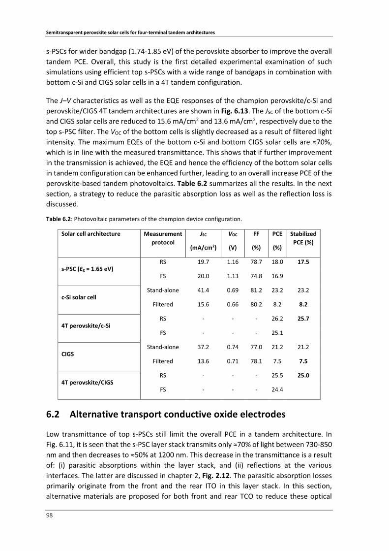
Semitransparent perovskite solar cells for four-terminal tandem architectures
98
s-PSCs for wider bandgap (1.74-1.85 eV) of the perovskite absorber to improve the overall
tandem PCE. Overall, this study is the first detailed experimental examination of such
simulations using efficient top s-PSCs with a wide range of bandgaps in combination with
bottom c-Si and CIGS solar cells in a 4T tandem configuration.
The J–V characteristics as well as the EQE responses of the champion perovskite/c‐Si and
perovskite/CIGS 4T tandem architectures are shown in Fig. 6.13. The JSC of the bottom c-Si
and CIGS solar cells are reduced to 15.6 mA/cm2 and 13.6 mA/cm2, respectively due to the
top s-PSC filter. The VOC of the bottom cells is slightly decreased as a result of filtered light
intensity. The maximum EQEs of the bottom c-Si and bottom CIGS solar cells are ≈70%,
which is in line with the measured transmittance. This shows that if further improvement
in the transmission is achieved, the EQE and hence the efficiency of the bottom solar cells
in tandem configuration can be enhanced further, leading to an overall increase PCE of the
perovskite-based tandem photovoltaics. Table 6.2 summarizes all the results. In the next
section, a strategy to reduce the parasitic absorption loss as well as the reflection loss is
discussed.
Table 6.2: Photovoltaic parameters of the champion device configuration.
Solar cell architecture Measurement
protocol
JSC
(mA/cm2)
VOC
(V)
FF
(%)
PCE
(%)
Stabilized
PCE (%)
s-PSC (Eg = 1.65 eV) RS 19.7 1.16 78.7 18.0 17.5
FS 20.0 1.13 74.8 16.9
c-Si solar cell Stand-alone 41.4 0.69 81.2 23.2 23.2
Filtered 15.6 0.66 80.2 8.2 8.2
4T perovskite/c-Si RS - - - 26.2 25.7
FS - - - 25.1
CIGS Stand-alone 37.2 0.74 77.0 21.2 21.2
Filtered 13.6 0.71 78.1 7.5 7.5
4T perovskite/CIGS RS - - - 25.5 25.0
FS - - - 24.4
6.2 Alternative transport conductive oxide electrodes
Low transmittance of top s-PSCs still limit the overall PCE in a tandem architecture. In
Fig. 6.11, it is seen that the s-PSC layer stack transmits only ≈70% of light between 730-850
nm and then decreases to ≈50% at 1200 nm. This decrease in the transmittance is a result
of: (i) parasitic absorptions within the layer stack, and (ii) reflections at the various
interfaces. The latter are discussed in chapter 2, Fig. 2.12. The parasitic absorption losses
primarily originate from the front and the rear ITO in this layer stack. In this section,
alternative materials are proposed for both front and rear TCO to reduce these optical

Semitransparent perovskite solar cells for four-terminal tandem architectures
99
losses and enhance the PCE in tandem architecture. To obtain insights about these TCO
electrodes, they are characterized by atomic force microscopy (AFM), XRD,
spectrophotometry, four-point probe measurements and hall-effect measurements.
Fig. 6.14: (a) Absorptance (A), (b) transmittance (T), (c) reflectance (R), (d) refractive index (n) and extinction coefficient (k), (e) the Tauc plot, and (f) x-ray diffraction of rear ITO and IZO. (g) and (h) shows the atomic force microscopy images of rear ITO and IZO, respectively.

Semitransparent perovskite solar cells for four-terminal tandem architectures
100
6.2.1 Rear TCOs for semitransparent perovskite solar cells
In order to reduce the absorption losses, a rear IZO electrode is developed. Details
regarding the deposition parameters are discussed in chapter 3. Spectrophotometric
measurements conducted on glass/TCO/air show a decrease in the absorptance of rear
IZO compared to ITO (5% absolute, see Fig. 6.14a, Table 6.3). This can be explained by the
significantly reduced extinction coefficient of the IZO in comparison to the ITO (Fig. 6.14d).
Notably, the absorptance is also decreased between 300-800 nm by 3.8% absolute.
Furthermore, a small reduction in the transmittance is also observed for the IZO in the near
infrared regime (Fig. 6.14b). This is due to the increase in reflectance at the IZO/air
interface, originating from the increased refractive index of the IZO (Fig. 6.14d). Since s-PSC
stack would either have an anti-reflection layer on the rear TCO or an index-matching layer
between the rear TCO of the s-PSC and the bottom cell in a 4T architecture, the increased
reflection loss observed here is not a major concern. Electrically, the rear IZO has a higher
sheet resistance than the ITO (Rsh ≈60 Ω/sq for IZO and Rsh ≈50 Ω/sq for ITO). In order to
compensate for the higher sheet resistances, gold grids are deposited on the rear TCO to
further increase the lateral conductivity (chapter 3, Fig. 3.3).99 Therefore, the increased
sheet resistance with the IZO should not affect the device performance considerably.
Furthermore, the lower bandgap of the IZO, which is evident from the Tauc plot (Fig.
6.14e), should not affect the performance of the s-PSCs as the photons in the ultra-violet
and visible wavelengths are absorbed by the perovskite layer before they reach the rear
electrode. XRD measurements are also performed to determine the crystallinity of the
TCOs. The results show that the rear IZO is amorphous, whereas the ITO is crystalline in
nature (Fig. 6.14f). Details regarding the crystallinity of the ITO are discussed in section
6.2.2. AFM images in Fig. 6.14g-h show that both ITO and IZO have similar surface
properties with roughness of ≈2 nm. However, some “particle-like” features are present
on the surface of both materials. For ITO, these features are more prominent and
approximately 10-12 nm in height, while for the IZO, these are slightly taller and ≈15-20 nm
Fig. 6.15: (a) Reflectance (R), (b) transmittance (T) and (c) absorptance (A) of the s-
PSC filters fabricated with rear ITO or IZO. The external quantum efficiencies (EQEs)
of the top s-PSC and bottom c-Si solar cell are also provided in (b) and (c), respectively.
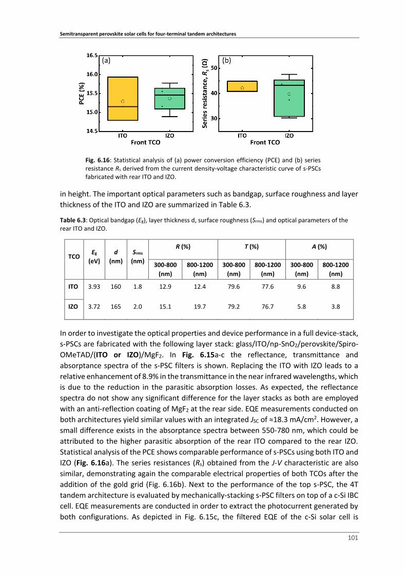
Semitransparent perovskite solar cells for four-terminal tandem architectures
101
in height. The important optical parameters such as bandgap, surface roughness and layer
thickness of the ITO and IZO are summarized in Table 6.3.
Table 6.3: Optical bandgap (Eg), layer thickness d, surface roughness (Srms) and optical parameters of the rear ITO and IZO.
TCO Eg
(eV)
d
(nm)
Srms
(nm)
R (%) T (%) A (%)
300-800
(nm)
800-1200
(nm)
300-800
(nm)
800-1200
(nm)
300-800
(nm)
800-1200
(nm)
ITO 3.93 160 1.8 12.9 12.4 79.6 77.6 9.6 8.8
IZO 3.72 165 2.0 15.1 19.7 79.2 76.7 5.8 3.8
In order to investigate the optical properties and device performance in a full device-stack,
s-PSCs are fabricated with the following layer stack: glass/ITO/np-SnO2/perovskite/Spiro-
OMeTAD/(ITO or IZO)/MgF2. In Fig. 6.15a-c the reflectance, transmittance and
absorptance spectra of the s-PSC filters is shown. Replacing the ITO with IZO leads to a
relative enhancement of 8.9% in the transmittance in the near infrared wavelengths, which
is due to the reduction in the parasitic absorption losses. As expected, the reflectance
spectra do not show any significant difference for the layer stacks as both are employed
with an anti-reflection coating of MgF2 at the rear side. EQE measurements conducted on
both architectures yield similar values with an integrated JSC of ≈18.3 mA/cm2. However, a
small difference exists in the absorptance spectra between 550-780 nm, which could be
attributed to the higher parasitic absorption of the rear ITO compared to the rear IZO.
Statistical analysis of the PCE shows comparable performance of s-PSCs using both ITO and
IZO (Fig. 6.16a). The series resistances (Rs) obtained from the J-V characteristic are also
similar, demonstrating again the comparable electrical properties of both TCOs after the
addition of the gold grid (Fig. 6.16b). Next to the performance of the top s-PSC, the 4T
tandem architecture is evaluated by mechanically-stacking s-PSC filters on top of a c-Si IBC
cell. EQE measurements are conducted in order to extract the photocurrent generated by
both configurations. As depicted in Fig. 6.15c, the filtered EQE of the c-Si solar cell is
Fig. 6.16: Statistical analysis of (a) power conversion efficiency (PCE) and (b) series resistance Rs derived from the current density-voltage characteristic curve of s-PSCs fabricated with rear ITO and IZO.

Semitransparent perovskite solar cells for four-terminal tandem architectures
102
enhanced in the case of IZO, leading to an increase in the integrated JSC by 1.1 mA/cm2
(enhancement of 7.7% relative). Overall, these results demonstrate that a rear IZO is a
better alternative to a rear ITO for 4T perovskite-based tandem solar cells.
6.2.2 Front TCOs for semitransparent perovskite solar cells
Another important factor to achieve high transmission and reduced reflection losses in a
s-PSC layer stack is to utilize a front TCO electrode having high refractive index along with
low extinction coefficient in the near infrared wavelengths. In the case of ITO, one strategy
would be to employ higher amount of oxygen during the sputtering process.132,200 This fills
Fig. 6.17: (a) Reflectance (R), (b) transmittance (T) and (c) absorptance (A), (d) refractive index (n), (e) extinction coefficient (k) and the Tauc plot of the commercial ITO, ITO with 12.5% O2 (ITOn) and IZO.

Semitransparent perovskite solar cells for four-terminal tandem architectures
103
up the oxygen vacancies and decreases the number of free charge carriers in ITO, which
leads to a shift in the plasma frequency of the ITO towards longer wavelengths. However,
the consequence of this is the increased sheet resistance, which must be compensated by
increasing the thickness of the ITO. In this work, 12.5% O2 content (much higher than the
standard process of 3.5% for the conventional front ITOv in our laboratory) is used to
prepare the front ITO and labelled as ITOn. Along with ITOn, other materials are
investigated that includes IZO or hydrogen-doped indium oxide (IO:H) as front TCO
electrodes. Here, an in-house front IZO is developed, while the IO:H is obtained from the
collaborator Zentrum für Sonnenenergie und Wasserstoff-Forschung Baden-Württemberg
(ZSW). All the above TCO electrodes are compared to a commercial ITO (similar to the front
ITO as discussed in section 6.1, also see Appendix Fig. A. 6.2 and Fig. A. 6.3 for
comparison), conventionally used to fabricate highly efficient o-PSCs. Further information
regarding the deposition parameters of ITOn, IZO and IO:H can be found in the chapter 3.
In the following, the optical and electrical properties of the available front TCO electrodes
are analyzed. Ellipsomentric measurements reveal an increase in the refractive indices for
ITOn, IZO and IO:H electrodes compared to commercial ITO (Fig. 6.17a), especially in the
near infrared wavelengths. At the same time, the extinction coefficients in the near
infrared wavelengths for these TCO electrodes are reduced (Fig. 6.17b). The decrease in
the extinction coefficient can be attributed to the reduction in the charge carrier
concentration (evaluated from Hall-effect measurements) by 1 order of magnitude
compared to the commercial ITO as shown in Table 6.4. Furthermore, spectrophotometric
measurements conducted on these TCOs on glass reveal an increased loss in reflections
(Fig. 6.17d), which is apparent due to the higher values in refractive indices. The
absorptance of these new TCO electrodes is reduced (Fig. 6.17e), which is also in line with
the obtained extinction coefficients. As discussed earlier, an increase in the thickness is
required to compensate for the reduced free charge carriers in the new TCO electrodes.
Therefore, ITOn, IZO and IO:H are deposited with thicknesses of 170 nm, 165 nm and 230
nm, respectively. Due to this, a shift in the maximum of the interferences is noted both in
transmittance and reflectance spectra for all the TCO electrodes. To investigate the
bandgaps of these TCO electrodes, Tauc plots are analyzed. Fig. 6.17c shows both ITOn and
IO:H have bandgaps (≥ 3.90 eV), which is highly important to reduce any parasitic
absorptions in short wavelength ranges. In contrast, IZO has a smaller bandgap of 3.83 eV,
which can potentially reduce photocurrents in top s-PSCs. In terms of electrical properties,
all the new TCO electrodes have low sheet resistances of ≈24 Ω/sq, however, they are still
slightly higher than the commercial ITO (≈15 Ω/sq). Hall-effect measurements reveal that
the mobility of the charge carriers in ITOn is similar to that of commercial ITO. Therefore,
for ITOn, the reduction in the carrier concentration is compensated mostly by the increased
thickness to maintain a low sheet resistance. In the case of IZO and IO:H, a significant
increase in the mobility is noted as shown in Table 6.4. Therefore, for these two TCOs, both
improved mobility and thicker layers played a role in maintaining low sheet resistances.

Semitransparent perovskite solar cells for four-terminal tandem architectures
104
Table 6.4: Layer thickness (d), surface roughness (Srms), bandgap (Eg), sheet resistance (Rsh) charge carrier mobility (µ) and charge carrier concentration (nc) of the front transparent conductive oxide electrodes.
TCO d (nm) Srms (nm) Eg (eV) Rsh (Ω/sq) µ (cm2/ V s) nc (cm-3)
ITO
(commercial)
140 4.1 4.05 15 35.1±3.90 1.05x10²¹
ITOn 170 2.1 3.92 24 36.5±6.30 0.39x10²¹
IZO 165 5.5 3.83 25 47.9±7.60 0.29x10²¹
IO:H 230 1.1 3.91 23 85.8±1.20 0.17x10²¹
In order to investigate the crystallinity of the deposited TCOs, XRD measurements are
performed (Fig. 6.18). Similar to the rear IZO, the front IZO is also amorphous. The
relatively broad peak observed in the XRD pattern originates from the glass substrate. It is
also noted that the ITOs (front and rear) and IO:H are crystalline in nature, and the crystal
planes are orientated preferentially along the (222) plane. In order to obtain more insights
about the crystallite size, the following Debye-Scherrer equation:201,202
𝐷 =
𝐾𝜆
𝛽𝑐𝑜𝑠𝜃
(6.1)
is used, where D is the crystallite size, K is the shape constant (0.9), β and θ are the full
width at half maximum and the Bragg’s angle (in radians) of the observed peak,
respectively. Table 6.5 summarizes the crystallite sizes for each of the planes. In general,
the crystallite sizes along the <222> plane for the front ITOs are smaller than the rear ITO.
Compared to the rear ITO that is processed at room temperature, the reduction of the
crystallite size for the front ITOn could be associated to a modification of the nucleation
kinetics at higher processing temperature (300 °C).203 Furthermore, a small shift (0.2°-0.3°)
Fig. 6.18: X-ray diffraction (XRD) pattern of the front transparent conductive oxide electrodes: commercial ITO, ITO with 12.5% O2 (ITOn) and IZO.

Semitransparent perovskite solar cells for four-terminal tandem architectures
105
towards the shorter angles is observed for all XRD peaks for the front ITOs compared to
that of the rear ITO. This is an indication that comparatively more Sn4+ ions, which are
smaller in size (0.71 Å) have replaced the indium (0.80 Å) sites, thus reducing the crystallite
size. Interestingly, the orientation of ITOn along the <400> plane is not observed in the XRD
pattern. This indicates that the O2 vacancies, which usually reside in this plane, are
significantly reduced or not present.204 This is line with the previous observations of slightly
higher sheet resistance and increased refractive index of the ITOn. Comparing commercial
ITO and ITOn with IO:H, considerably sharper reflection peaks with reduced full-width half
maxima (FWHM) are noticed. This indicates very high crystallinity of IO:H. This high
crystallinity could be associated to the post thermal treatment, which crystallizes the
amorphous IO:H deposited at the time of sputtering.36 Due to this high crystallinity, the
crystallite size is also increased. This is an indication that the number of the grain
boundaries in IO:H could be reduced compared to the ITOs, resulting in high mobility of
the charge carriers.
AFM measurements conducted on the TCOs show that the developed ITOn is more
compact than the commercial front ITO (Fig. 6.19). The surface roughness for the all the
TCOs is below 6 nm. Interestingly, the IO:H depicts a surface roughness of only ≈1.1 nm.
Furthermore, similar to the rear TCOs, the front IZO also shows small features, which are
distributed all over the substrates. In order to further investigate the performance of TCOs
in tandem architectures, in the next section, an in-depth discussion is presented comparing
their photovoltaic performance.
Fig. 6.19: Atomic force microscopy (AFM) images of the commercial (a) ITO, (b) ITOn (c) IZO and (d) IO:H electrodes.

Semitransparent perovskite solar cells for four-terminal tandem architectures
106
Table 6.5: Analysis of the x-ray diffraction (XRD) spectra of the transparent conductive oxide (TCO) electrodes.
TCO Plane (hlk) 2θ (°) FWHM (°) Crystallite size, D (nm)
ITO
(commercial)
211 21.5 0.257 31.46
222 30.4 0.439 18.75
400 35.4 0.264 31.58
440 50.7 0.473 18.58
622 60.3 0.484 18.98
ITOn
211 21.3 0.285 28.36
222 30.3 0.476 17.29
400 - - -
440 50.5 0.452 19.4
622 - - -
Rear ITO
211 21.2 0.251 32.20
222 30.1 0.310 26.53
400 35.2 0.168 49.60
440 50.5 0.324 27.11
622 60.1 0.345 26.60
IO:H
211 21.5 0.158 51.17
222 30.6 0.172 47.88
400 35.5 0.175 47.66
440 51.0 0.273 32.24
622 60.7 0.290 31.74
6.3 Photovoltaic characteristics of perovskite solar cells with
various TCOs
The improved optical properties of the TCOs lead to an enhanced photovoltaic
performance of the perovskite/c-Si tandem solar cells. In order to demonstrate this, s-PSCs
are fabricated in the following layer stack: glass/(Commercial ITO or ITOn or IZO or
IO:H/np-SnO2/perovskite/Spiro-OMeTAD/MoOX/IZO/MgF2. As the absorber, a triple
cation (Cs0.1(MA0.17FA0.83)0.9Pb(I0.83Br0.17)3) perovskite is deposited. A rear IZO is used
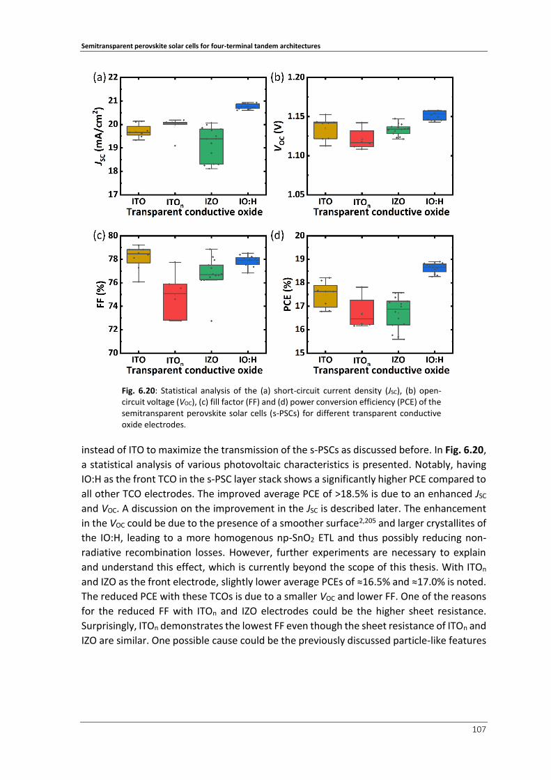
Semitransparent perovskite solar cells for four-terminal tandem architectures
107
instead of ITO to maximize the transmission of the s-PSCs as discussed before. In Fig. 6.20,
a statistical analysis of various photovoltaic characteristics is presented. Notably, having
IO:H as the front TCO in the s-PSC layer stack shows a significantly higher PCE compared to
all other TCO electrodes. The improved average PCE of >18.5% is due to an enhanced JSC
and VOC. A discussion on the improvement in the JSC is described later. The enhancement
in the VOC could be due to the presence of a smoother surface2,205 and larger crystallites of
the IO:H, leading to a more homogenous np-SnO2 ETL and thus possibly reducing non-
radiative recombination losses. However, further experiments are necessary to explain
and understand this effect, which is currently beyond the scope of this thesis. With ITOn
and IZO as the front electrode, slightly lower average PCEs of ≈16.5% and ≈17.0% is noted.
The reduced PCE with these TCOs is due to a smaller VOC and lower FF. One of the reasons
for the reduced FF with ITOn and IZO electrodes could be the higher sheet resistance.
Surprisingly, ITOn demonstrates the lowest FF even though the sheet resistance of ITOn and
IZO are similar. One possible cause could be the previously discussed particle-like features
Fig. 6.20: Statistical analysis of the (a) short-circuit current density (JSC), (b) open-circuit voltage (VOC), (c) fill factor (FF) and (d) power conversion efficiency (PCE) of the semitransparent perovskite solar cells (s-PSCs) for different transparent conductive oxide electrodes.

Semitransparent perovskite solar cells for four-terminal tandem architectures
108
as shown in the AFM images (Fig. 6.19) that may lead to shunting paths in these devices.
However, detailed experimental investigation is necessary in this context.
In terms of JSC, s-PSCs with IO:H demonstrate the highest photocurrents. To comprehend
the differences in the JSC between these devices, EQE measurements are conducted
(Fig. 6.21a). For IO:H, a broadband enhancement is observed from 500 nm up to the
bandgap of the perovskite. This improvement can be ascribed to the reduced reflections
as shown Fig. 6.21b. Compared to the commercial ITO, a shift in the peak of the EQE
spectra is noted for all the TCO electrodes. This is also in line with the absorptance spectra
of the s-PSCs (Fig. 6.21c) and it arises due to the difference in the thickness of these TCO
electrodes as mentioned before. Interestingly, for ITOn and IZO, this shift results in a better
matching of the EQE maximum to the AM 1.5G irradiation spectra maximum. As a result,
a slightly improved JSC is obtained with ITOn. In case of IZO, the apparent lower average JSC
is associated to the smaller bandgap of the IZO, which is noticeable in the EQE spectrum.
The J-V characteristics of the champion devices with different TCO electrodes are
presented in Fig. 6.22. The results show that all devices exhibit hysteresis, however, the
Fig. 6.21: (a) External quantum efficiency (EQE) of the top semitransparent perovskite solar cells (s-PSCs) and filtered bottom crystalline-silicon (c-Si) solar cells for different transparent conductive oxide electrodes. (b) Reflectance (R), (c) absorptance (A) and (d) transmittance (T) spectra of the s-PSC filters for different transparent conductive oxide electrodes.

Semitransparent perovskite solar cells for four-terminal tandem architectures
109
smallest is observed for IO:H. In order to obtain the PCE at MPP, the s-PSCs are measured
for 5 minutes under light and at constant voltage near the MPP. Consistent to the J-V
characteristics discussed earlier, the s-PSCs with IO:H exhibit the highest PCE of 18.1%.
s-PSCs fabricated with all the TCOs show no sign of degradation within this short period of
time. Further details regarding the photovoltaic parameters for these TCO electrodes can
be found in Table 6.6.
Before investigating the performance of the 4T perovskite/c-Si tandem solar cell with these
TCO electrodes, the transmittance of the s-PSCs is analyzed (Fig. 6.21d). Compared to the
commercial ITO, a significantly enhanced transmittance in the near infrared wavelengths
is observed for the in-house sputtered TCO electrodes. For IO:H, which already
demonstrated to be the better TCO among the four in top s-PSC configuration, the highest
transmittance of >85% is also noted for this TCO. The improved transmittance is a result
of both reduced reflections and parasitic absorptions as shown in Fig. 6.21b-c. While the
reflection losses are reduced as these TCOs have high refractive indices compared to
commercial ITO, the parasitic absorptions are reduced due to a reduced number of charge
carriers.
Fig. 6.22: Current density-voltage (J–V) characteristics of the champion top semitransparent perovskite solar cells (s-PSCs) fabricated with (a) ITO, (b) ITOn, (c) IZO and (d) IO:H. The inset corresponds to the stabilized power conversion efficiency (PCE) measured at constant voltages near the maximum power point.
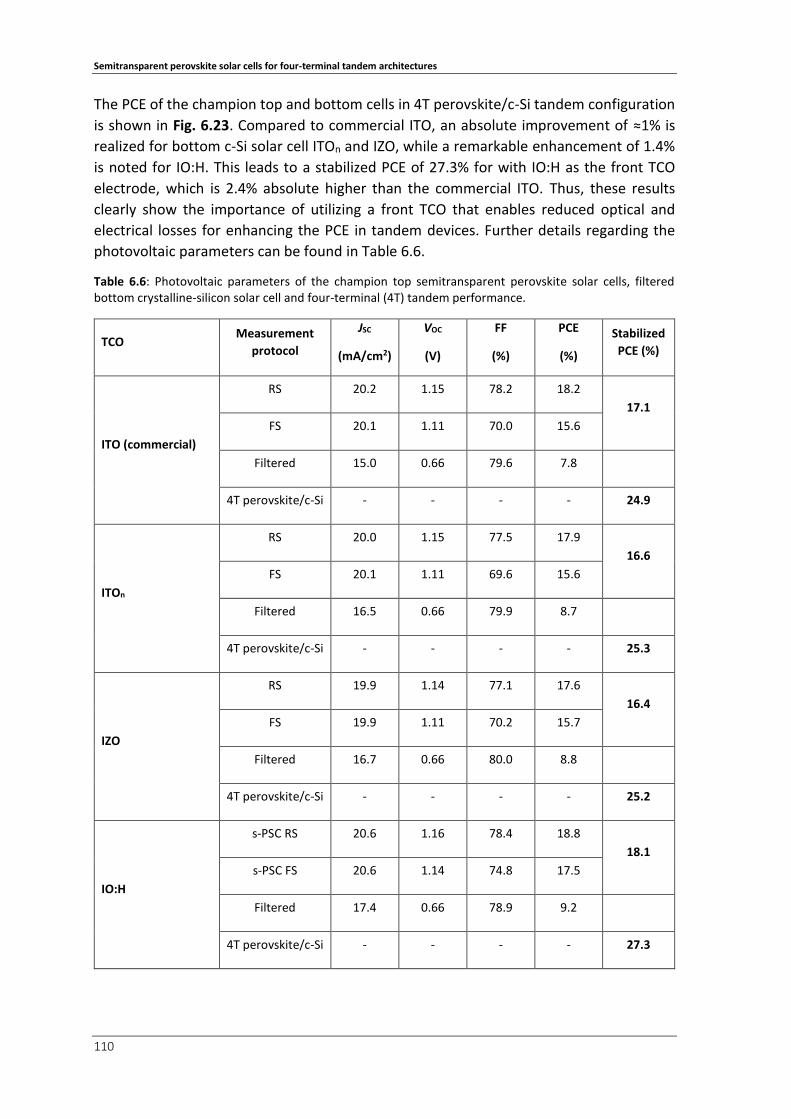
Semitransparent perovskite solar cells for four-terminal tandem architectures
110
The PCE of the champion top and bottom cells in 4T perovskite/c-Si tandem configuration
is shown in Fig. 6.23. Compared to commercial ITO, an absolute improvement of ≈1% is
realized for bottom c-Si solar cell ITOn and IZO, while a remarkable enhancement of 1.4%
is noted for IO:H. This leads to a stabilized PCE of 27.3% for with IO:H as the front TCO
electrode, which is 2.4% absolute higher than the commercial ITO. Thus, these results
clearly show the importance of utilizing a front TCO that enables reduced optical and
electrical losses for enhancing the PCE in tandem devices. Further details regarding the
photovoltaic parameters can be found in Table 6.6.
Table 6.6: Photovoltaic parameters of the champion top semitransparent perovskite solar cells, filtered bottom crystalline-silicon solar cell and four-terminal (4T) tandem performance.
TCO Measurement
protocol
JSC
(mA/cm2)
VOC
(V)
FF
(%)
PCE
(%)
Stabilized
PCE (%)
ITO (commercial)
RS 20.2 1.15 78.2 18.2
17.1
FS 20.1 1.11 70.0 15.6
Filtered 15.0 0.66 79.6 7.8
4T perovskite/c-Si - - - - 24.9
ITOn
RS 20.0 1.15 77.5 17.9
16.6
FS 20.1 1.11 69.6 15.6
Filtered 16.5 0.66 79.9 8.7
4T perovskite/c-Si - - - - 25.3
IZO
RS 19.9 1.14 77.1 17.6
16.4
FS 19.9 1.11 70.2 15.7
Filtered 16.7 0.66 80.0 8.8
4T perovskite/c-Si - - - - 25.2
IO:H
s-PSC RS 20.6 1.16 78.4 18.8
18.1
s-PSC FS 20.6 1.14 74.8 17.5
Filtered 17.4 0.66 78.9 9.2
4T perovskite/c-Si - - - - 27.3
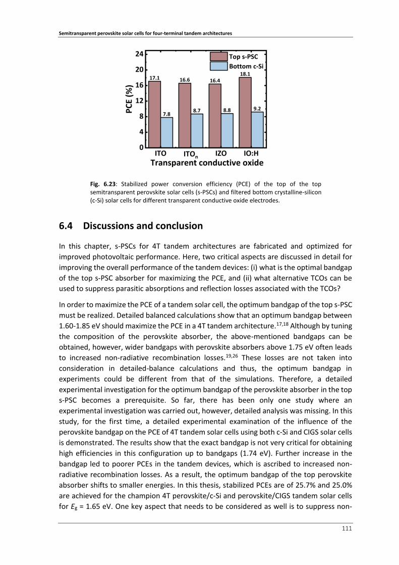
Semitransparent perovskite solar cells for four-terminal tandem architectures
111
6.4 Discussions and conclusion
In this chapter, s-PSCs for 4T tandem architectures are fabricated and optimized for
improved photovoltaic performance. Here, two critical aspects are discussed in detail for
improving the overall performance of the tandem devices: (i) what is the optimal bandgap
of the top s-PSC absorber for maximizing the PCE, and (ii) what alternative TCOs can be
used to suppress parasitic absorptions and reflection losses associated with the TCOs?
In order to maximize the PCE of a tandem solar cell, the optimum bandgap of the top s-PSC
must be realized. Detailed balanced calculations show that an optimum bandgap between
1.60-1.85 eV should maximize the PCE in a 4T tandem architecture.17,18 Although by tuning
the composition of the perovskite absorber, the above-mentioned bandgaps can be
obtained, however, wider bandgaps with perovskite absorbers above 1.75 eV often leads
to increased non-radiative recombination losses.19,26 These losses are not taken into
consideration in detailed-balance calculations and thus, the optimum bandgap in
experiments could be different from that of the simulations. Therefore, a detailed
experimental investigation for the optimum bandgap of the perovskite absorber in the top
s-PSC becomes a prerequisite. So far, there has been only one study where an
experimental investigation was carried out, however, detailed analysis was missing. In this
study, for the first time, a detailed experimental examination of the influence of the
perovskite bandgap on the PCE of 4T tandem solar cells using both c-Si and CIGS solar cells
is demonstrated. The results show that the exact bandgap is not very critical for obtaining
high efficiencies in this configuration up to bandgaps (1.74 eV). Further increase in the
bandgap led to poorer PCEs in the tandem devices, which is ascribed to increased non-
radiative recombination losses. As a result, the optimum bandgap of the top perovskite
absorber shifts to smaller energies. In this thesis, stabilized PCEs are of 25.7% and 25.0%
are achieved for the champion 4T perovskite/c-Si and perovskite/CIGS tandem solar cells
for Eg = 1.65 eV. One key aspect that needs to be considered as well is to suppress non-
Fig. 6.23: Stabilized power conversion efficiency (PCE) of the top of the top semitransparent perovskite solar cells (s-PSCs) and filtered bottom crystalline-silicon (c-Si) solar cells for different transparent conductive oxide electrodes.

Semitransparent perovskite solar cells for four-terminal tandem architectures
112
radiative recombination losses in the bulk or at the interfaces of the perovskite layer. For
this, here a 2D/3D perovskite heterostructure is employed by spin-coating
n-butylammonium bromide on top of the perovskite absorber, which reduces non-
radiative recombination losses at the perovskite/HTL interface, and the fabricated devices
exhibit an enhanced VOC of around 45 mV.
In the second part of this chapter, the influence of the front and the rear TCO electrodes
on the performance of 4T perovskite/c-Si tandem solar cells is investigated. While the rear
ITO shows significant parasitic absorption losses, the front commercial ITO, which is widely
used to fabricate highly efficient opaque PSCs, incurs significant parasitic and reflection
losses in the near infrared wavelengths. These losses affect the PCE in the bottom solar
cell of the tandem device. The losses arise due the presence of high carrier concentration
in the ITO for maintaining low sheet resistances. By replacing the rear ITO with an IZO
electrode, the parasitic absorption losses are significantly reduced, leading to an enhanced
transmittance of 8.9% relative in the near infrared wavelengths. Furthermore, it is
demonstrated that by replacing the commercial ITO with TCO electrodes having reduced
charge carrier concentration (ITOn/IZO) and improved mobility (IZO and IO:H), these
reflection and parasitic absorption losses are suppressed significantly. This leads to an
enhanced transmittance (>85% for IO:H) for the s-PSCs fabricated with these TCO
electrodes. In other research groups, similar transmittance was realized but they required
to have additional micro-textured foils at the front air/glass interface that reduced
reflection losses.13,34 Within the new TCO electrode investigated in this study, the highest
PCE is demonstrated with IO:H, demonstrating a stabilized efficiency of 27.3% for the 4T
tandem configuration, one of the highest PCE recorded in 4T tandem architecture to date.
Thus, these results show that it is highly important to consider alternative TCOs for the
application in perovskite-based tandem devices.
113
7. Conclusion and outlook
To date, the power conversion efficiencies (PCE) of perovskite/crystalline-silicon tandem
solar cells have surpassed the PCE of market-dominating single-junction crystalline-silicon
(c-Si) solar cells. However, these tandem solar cells still suffer from various optical and
electrical losses. While optical losses mainly arise due to reflections and parasitic
absorptions due to the transparent conductive oxide (TCO) electrodes, and the non-ideal
bandgap of the perovskite absorber, electrical losses appear because of non-radiative
recombination or poor extraction of generated charge carriers. This thesis presents
multiple strategies for reducing optical losses and improving the PCE of perovskite-based
tandem solar cells.
Highly efficient perovskite solar cells conventionally use electron transport layers (ETLs)
that require a high-processing temperature (> 450 °C).31–34 This high-processing
temperature limits perovskite solar cells to TCOs that are strongly absorbing and therefore,
not ideal for high efficiency perovskite-based tandem solar cells. Hence, as a first strategy
to reduce optical losses in perovskites solar cells, alternative electron transport layers
(ETLs) are investigated. These ETLs comprise of nanoparticles of TiO2 (np-TiO2) and
nanoparticles of SnO2 (np-SnO2), which can be deposited at a lower temperature (i.e.,
100 °C for np-TiO2 and 150 °C for np-SnO2). The ability to deposit np-TiO2 and np-SnO2 at a
significantly reduced temperature made these materials compatible with TCO electrodes
that exhibit low near infrared parasitic absorptions, such as ITO, IZO and IO:H.36,37 Thus,
these nanoparticle-based ETLs play a critical role in terms of minimizing the optical losses
in perovskite-based tandem solar cells. Furthermore, a detailed comparative study
between the two ETLs reveal that np-SnO2 based PSCs present less hysteresis and
improved charge carrier extraction, making it a more promising ETL candidate. However,
np-TiO2 allow more flexibility in terms of tuning various material properties as they are
synthesized in-house. This includes enhancing the conductivity of np-TiO2 by doping it with
Nb5+, which is critical where thick ETLs are required. Furthermore, the ability to disperse
the np-TiO2 in various solvent systems makes them compatible with various roll-to-roll
processing techniques such as inkjet printing, blade coating, and slot-die coating.
As a second strategy to reduce optical losses, nanophotonic light management concepts
or alternative materials for TCOs are explored. The discussions on nanophotonic light
management concept can be found in chapter 5, while in chapter 6 alternative materials
for TCOs are discussed. Compared to conventional light management concepts, such as
microtextured foils58,63 or anti-reflection coatings184 at the front side of a tandem solar cell,
in this thesis nanophotonic light management is employed by fabricating nanostructured
ITO (NS ITO) electrodes. The NS ITO electrodes enable improved light in-coupling by
forming an effective refractive index medium. Two approaches are presented to obtain
this NS ITO: (i) soft-imprinting to fabricate periodic nanostructures and (ii) polymer blend
lithography to fabricate disordered nanostructures. Both demonstrate respective relative
enhancements of up to ≈5% and ≈7% relative, over a broad range of wavelengths
(300-1200 nm). Due to the reduction of reflection losses, improved short-circuit current

Conclusion and outlook
114
densities of ≈2-3% relative and ≈23% relative for top perovskite and bottom crystalline-
silicon (c-Si) solar cells respectively, are achieved. However, a poor open-circuit voltage
(VOC) and a reduced fill factor (FF) for semitransparent perovskite solar cells (s-PSCs) with
NS ITO leads to only a 0.7% absolute increase in the PCE for 4T perovskite/c-Si tandem
solar cells. Further analysis is performed to determine the potential improvement by NS
ITO. Considering a similar VOC and FF from both NS ITO and reference planar ITO devices,
a potential increase of 2.1% absolute in PCE is expected.
As alternative materials for the reduction of optical losses in TCOs, an in-house sputtering
technique is employed to fabricate front TCO electrodes that exhibit reduced carrier
concentration in chapter 6. Due to the reduced carrier concentration, an improvement of
transmission in the near infrared wavelengths is achieved for the s-PSCs. Transmittance of
>85% is demonstrated with IO:H, which enhanced the absolute PCE in the bottom c-Si solar
cell by 1.4%. As a result, 4T perovskite/c-Si tandem solar cells with PCE up to 27.3% have
been achieved. This PCE is one of the highest recorded PCEs in a 4T perovskite/c-Si tandem
architecture to date. Furthermore, it is shown that replacing the highly absorbing rear ITO
with a rear IZO layer in a s-PSC improves the transmission significantly in the near infrared
wavelengths.
Finally, in order to maximize the PCE of the perovskite-based tandem PV and to determine
the optimum bandgap of the top perovskite absorber, a detailed experimental
investigation is carried out for perovskite/c-Si and perovskite/CIGS tandem solar cells in a
4T tandem configuration. The results reveal that the exact bandgap of the top perovskite
absorber is not a critical requirement for obtaining high efficiencies. With bandgaps
between 1.65-1.74 eV, comparable and yet high PCEs are achieved, which is in line with
detailed-balance calculations. A deviation in the trend compared to the detailed-balance
analysis is noted when much wider bandgaps (1.74-1.85 eV) of the perovskite absorber are
used. This is due to the increased VOC loss for these bandgaps. In this study, a surface
passivation technique using a 2D/3D heterostucture has been employed to mitigate
defects and non-radiative recombination process at the perovskite/hole transport layer
interface. Although the VOC loss for the bandgap range (1.74-1.85 eV) still remains, an
overall improvement of ≈45 mV is achieved for bandgaps between 1.65 eV and 1.85 eV.
The loss in VOC for the bandgap range 1.74-1.85 eV occurs due to the presence of high
amounts of bromide ions. These high amounts of bromide ions promote phase-segregation
under illumination and lead to a poorer device performance.
7.1 Outlook
Although various strategies are presented in this thesis to reduce optical losses and
improve the PCE of perovskite-based tandem solar cells, further improvements are still
possible. In this section, an outlook is presented that discusses various ways in further
enhancing the performances.
While this thesis employs np-TiO2 as the ETL for n-i-p perovskite solar cells, dispersing
these np-TiO2 in other solvents such as chlorobenzene or toluene would mean they could

Conclusion and outlook
115
likely be used in the p-i-n architecture (inverted architecture) of perovskite solar cells as
well. This implies that np-TiO2 can be deposited on top of the perovskite absorber layer.
The advantage of np-TiO2 in the p-i-n architecture would be to circumvent the common
combination of organic ETL (C60) and with a buffer layer of atomic layer deposited SnO2.80
As a result, the layer stack would be simplified and can potentially improve the long-term
stability of perovskite solar cells.
In terms of nanophotonic front electrodes, several aspects can be investigated in future
studies. The significant potential improvement of by 2.1% highlights the importance of
overcoming VOC losses in NS ITO based tandem devices. In order to overcome this VOC loss,
different deposition methods for the charge transport layer or alternative materials can be
explored to improve the NS ITO and the subsequent layer interface that is the root of the
observed increase in non-radiative recombination. Future studies can investigate
thermal80 or electron beam evaporation,108,206 or sputtering techniques207 to deposit
high-quality charge transport layers and improve said interface. As alternative materials,
self-assembled monolayers may also be employed.120 In a recent study, perovskite solar
cells with nanostructured TCO exhibited very small VOC losses when they employed such
self-assembled monolayers.43 Another important aspect, which is highly important to
consider for the NS ITO is the formation of cracks between the nanostructures. These
cracks are the probable cause of increased sheet resistance for nanostructures with
smaller geometries. Although the effect of increased sheet resistance is not so severe in
s-PSCs that are fabricated in this thesis (because the area is small at only 10.5 mm2), any
large-area PSCs will observe a significant detrimental effect on their PCE. In order to reduce
sheet resistance, future studies can include investigations of different sputtering
conditions or the use of metal grids for NS TCO.15,58 Next to this, it is also important to
employ different strategies to transfer the nanostructures directly to the glass
substrate,208,209 thus circumventing the usage of polystyrene that limits the processing
temperature210 of the PSC and long-term stability.
With respect to further improving the transmission, a rear IO:H TCO can be investigated.
As IO:H absorbs below 5% of light in the near infrared wavelengths shown in this thesis, a
further increase in the transmission would be possible if the rear IZO is replaced with a
rear IO:H. One challenge to deposit this high-quality IO:H as a rear electrode is the
requirement for a post annealing crystallization at ≈200 °C. This high temperature is not
suitable for perovskite absorbers used here as they are prone to degradation from thermal
stress. Therefore, future works can include an investigation into reducing the
crystallization temperature of IO:H to deposit it as a rear TCO in s-PSCs for perovskite-
based tandem PV.
In regard to the optimization of the bandgap for perovskite-based tandem devices, future
studies can involve improving the s-PSC performance for wider bandgap materials. One
possible way is to deposit perovskite absorbers with higher amounts of cesium ions. It has
been reported that increasing the amount of the monovalent cation cesium in the crystal
structure raises the bandgap of the perovskite absorber.25 Therefore, future studies can

Conclusion and outlook
116
involve a closer look at various other monovalent cations and their impact in reducing
phase-segregation.

117
Appendix
Appendix for Chapter 4
Fig. A. 4.1: Absorptance of ITO and FTO.
Fig. A. 4.2: Scanning electron microscopy image of perovskite (CH3NH3PbI3) absorber on np-TiO2 deposited by spin coating, inkjet printing and blade coating. Reproduced with permission from ACS Applier Energy Materials, [139] © American Chemical Society.
Fig. A. 4.3: Grain size distribution of the perovskite absorber on np-TiO2 deposited by spin coating, inkjet
printing and blade coating. Reproduced with permission from ACS Applier Energy Materials, [139] © American
Chemical Society.
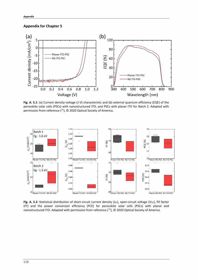
Appendix
118
Appendix for Chapter 5
Fig. A. 5.1: (a) Current density-voltage (J-V) characteristic and (b) external quantum efficiency (EQE) of the perovskite solar cells (PSCs) with nanostructured ITO, and PSCs with planar ITO for Batch 2. Adapted with permission from reference [71], © 2020 Optical Society of America.
Fig. A. 5.2: Statistical distribution of short-circuit current density (JSC), open-circuit voltage (VOC), fill factor (FF) and the power conversion efficiency (PCE) for perovskite solar cells (PSCs) with planar and nanostructured ITO. Adapted with permission from reference [71], © 2020 Optical Society of America.

Appendix
119
Fig. A. 5.3: Schematic of interdigitated back contact crystalline-silicon (c-Si) bottom solar cell. Adapted with permission from reference [71], © 2020 Optical Society of America.
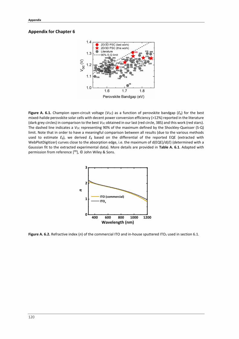
Appendix
120
Appendix for Chapter 6
Figure A. 6.1. Champion open-circuit voltage (VOC) as a function of perovskite bandgap (Eg) for the best mixed-halide perovskite solar cells with decent power conversion efficiency (>12%) reported in the literature (dark grey circles) in comparison to the best VOC obtained in our last (red circle, 38S) and this work (red stars). The dashed line indicates a VOC representing 90% of the maximum defined by the Shockley-Queisser (S-Q) limit. Note that in order to have a meaningful comparison between all results (due to the various methods used to estimate Eg), we derived Eg based on the differential of the reported EQE (extracted with WebPlotDigitizer) curves close to the absorption edge, i.e. the maximum of d(EQE)/d(E) (determined with a Gaussian fit to the extracted experimental data). More details are provided in Table A. 6.1. Adapted with permission from reference [99], © John Wiley & Sons.
Figure A. 6.2. Refractive index (n) of the commercial ITO and in-house sputtered ITOv used in section 6.1.
400 600 800 1000 12000
1
2
3
n
Wavelength (nm)
ITO (commercial)
ITOv
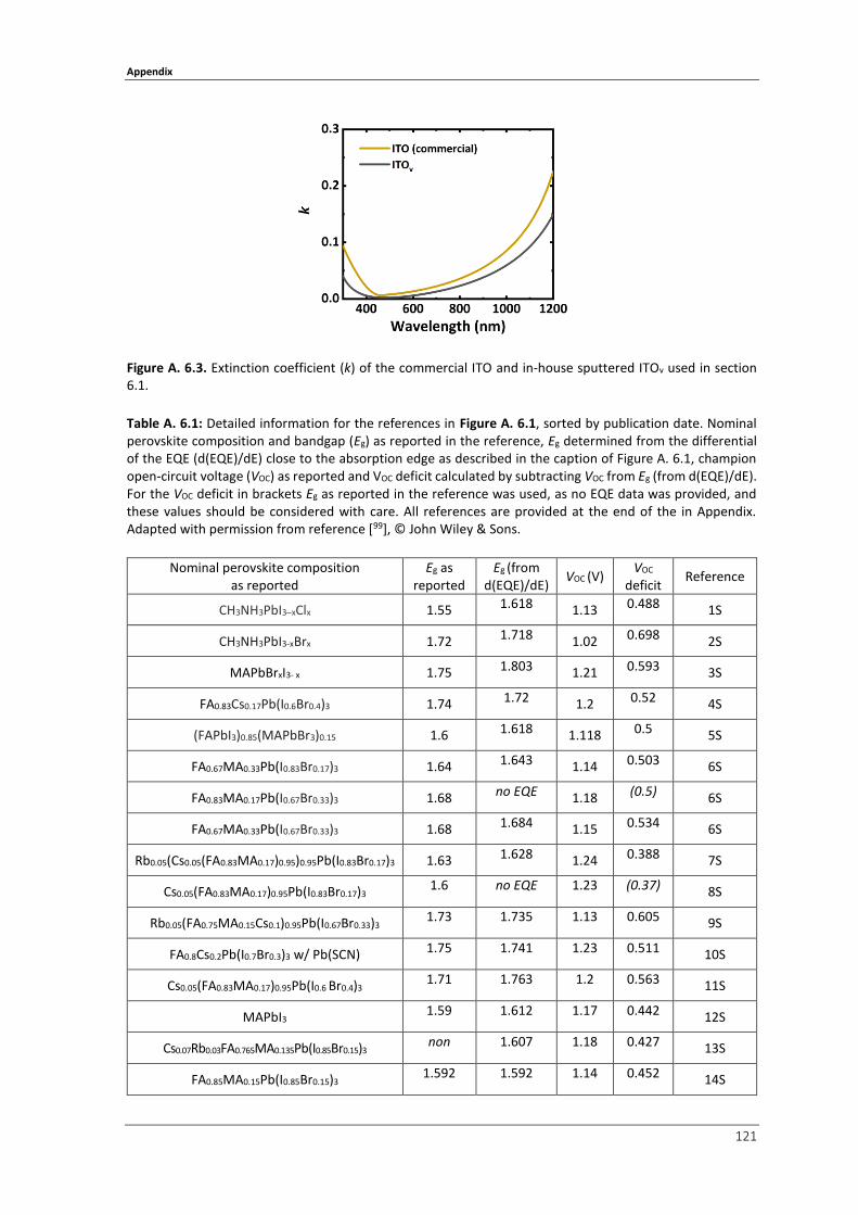
Appendix
121
Figure A. 6.3. Extinction coefficient (k) of the commercial ITO and in-house sputtered ITOv used in section 6.1.
Table A. 6.1: Detailed information for the references in Figure A. 6.1, sorted by publication date. Nominal perovskite composition and bandgap (Eg) as reported in the reference, Eg determined from the differential of the EQE (d(EQE)/dE) close to the absorption edge as described in the caption of Figure A. 6.1, champion open-circuit voltage (VOC) as reported and VOC deficit calculated by subtracting VOC from Eg (from d(EQE)/dE). For the VOC deficit in brackets Eg as reported in the reference was used, as no EQE data was provided, and these values should be considered with care. All references are provided at the end of the in Appendix. Adapted with permission from reference [99], © John Wiley & Sons.
Nominal perovskite composition as reported
Eg as reported
Eg (from d(EQE)/dE)
VOC (V) VOC
deficit Reference
CH3NH3PbI3–xClx 1.55 1.618 1.13 0.488 1S
CH3NH3PbI3‐xBrx 1.72 1.718 1.02 0.698 2S
MAPbBrxI3- x 1.75 1.803 1.21 0.593 3S
FA0.83Cs0.17Pb(I0.6Br0.4)3 1.74 1.72 1.2 0.52 4S
(FAPbI3)0.85(MAPbBr3)0.15 1.6 1.618 1.118 0.5 5S
FA0.67MA0.33Pb(I0.83Br0.17)3 1.64 1.643 1.14 0.503 6S
FA0.83MA0.17Pb(I0.67Br0.33)3 1.68 no EQE 1.18 (0.5) 6S
FA0.67MA0.33Pb(I0.67Br0.33)3 1.68 1.684 1.15 0.534 6S
Rb0.05(Cs0.05(FA0.83MA0.17)0.95)0.95Pb(I0.83Br0.17)3 1.63 1.628 1.24 0.388 7S
Cs0.05(FA0.83MA0.17)0.95Pb(I0.83Br0.17)3 1.6 no EQE 1.23 (0.37) 8S
Rb0.05(FA0.75MA0.15Cs0.1)0.95Pb(I0.67Br0.33)3 1.73 1.735 1.13 0.605 9S
FA0.8Cs0.2Pb(I0.7Br0.3)3 w/ Pb(SCN) 1.75 1.741 1.23 0.511 10S
Cs0.05(FA0.83MA0.17)0.95Pb(I0.6 Br0.4)3 1.71 1.763 1.2 0.563 11S
MAPbI3 1.59 1.612 1.17 0.442 12S
Cs0.07Rb0.03FA0.765MA0.135Pb(I0.85Br0.15)3 non 1.607 1.18 0.427 13S
FA0.85MA0.15Pb(I0.85Br0.15)3 1.592 1.592 1.14 0.452 14S
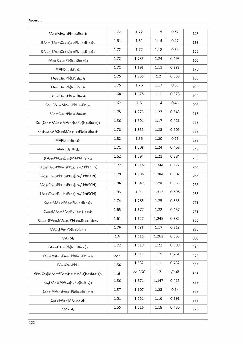
Appendix
122
FA0.83MA0.17Pb(I0.6Br0.4)3 1.72 1.72 1.15 0.57 14S
BA0.05(FA0.83Cs0.17)0.95Pb(I0.8Br0.2)3 1.61 1.61 1.14 0.47 15S
BA0.09(FA0.83Cs0.17)0.91Pb(I0.6Br0.4)3 1.72 1.72 1.18 0.54 15S
FA0.85Cs0.15Pb(I0.73Br0.27)3 1.72 1.735 1.24 0.495 16S
MAPb(I0.8Br0.2)3 1.72 1.695 1.11 0.585 17S
FA0.8Cs0.2Pb(Br0.3I0.7)3 1.75 1.739 1.2 0.539 18S
FA0.6Cs0.4Pb(I0.7Br0.3)3 1.75 1.76 1.17 0.59 19S
FA0.75Cs0.25Pb(I0.8Br0.2)3 1.68 1.678 1.1 0.578 19S
Cs0.1FA0.74MA0.13PbI2.48Br0.39 1.62 1.6 1.14 0.46 20S
FA0.83Cs0.17Pb(I0.6Br0.4)3 1.75 1.773 1.23 0.543 21S
K0.1(Cs0.06FA00.79MA0.15)0.9Pb(I0.85Br0.15)3 1.56 1.591 1.17 0.421 22S
K0.1(Cs0.06FA00.79MA0.15)0.9Pb(I0.4Br0.6)3 1.78 1.835 1.23 0.605 22S
MAPb(I0.6Br0.4)3 1.82 1.83 1.30 0.53 23S
MAPb(I1-xBrx)3 1.71 1.708 1.24 0.468 24S
(FA0.95PbI2.95)0.85(MAPbBr3)0.15 1.62 1.594 1.21 0.384 25S
FA0.83Cs0.17Pb(I0.73Br0.27)3 w/ Pb(SCN) 1.72 1.716 1.244 0.472 26S
FA0.83Cs0.17Pb(I0.6Br0.4)3 w/ Pb(SCN) 1.79 1.786 1.284 0.502 26S
FA0.83Cs0.17Pb(I0.5Br0.5)3 w/ Pb(SCN) 1.86 1.849 1.296 0.553 26S
FA0.83Cs0.17Pb(I0.4Br0.6)3 w/ Pb(SCN) 1.93 1.91 1.312 0.598 26S
Cs0.12MA0.05FA0.83Pb(I0.6Br0.4)3 1.74 1.785 1.25 0.535 27S
Cs0.05MA0.15FA0.8Pb(I0.75Br0.25)3 1.65 1.677 1.22 0.457 27S
Cs0.05((FA0.85MA0.15)Pb(I0.85Br0.15)3)0.95 1.61 1.627 1.245 0.382 28S
MA0.6FA0.4Pb(I0.6Br0.4)3 1.76 1.788 1.17 0.618 29S
MAPbI3 1.6 1.615 1.262 0.353 30S
FA0.85Cs0.15Pb(I0.71Br0.29)3 1.72 1.819 1.22 0.599 31S
Cs0.05MA0.14FA0.81Pb(I0.85Br0.15)3 non 1.611 1.15 0.461 32S
FA0.8Cs0.2PbI3 1.56 1.532 1.1 0.432 33S
GA5(Cs5(MA0.17FA0.83)0.95)0.95Pb(I0.83Br0.17)3 1.6 no EQE 1.2 (0.4) 34S
Csy(FA0.57MA0.43)1-yPb(I1-xBrx)3 1.56 1.571 1.147 0.413 35S
Cs0.05MA0.14FA0.81Pb(I0.85Br0.15)3 1.57 1.607 1.23 0.34 36S
Cs0.05FA0.70MA0.25PbI3 1.51 1.551 1.16 0.391 37S
MAPbI3 1.55 1.616 1.18 0.436 37S
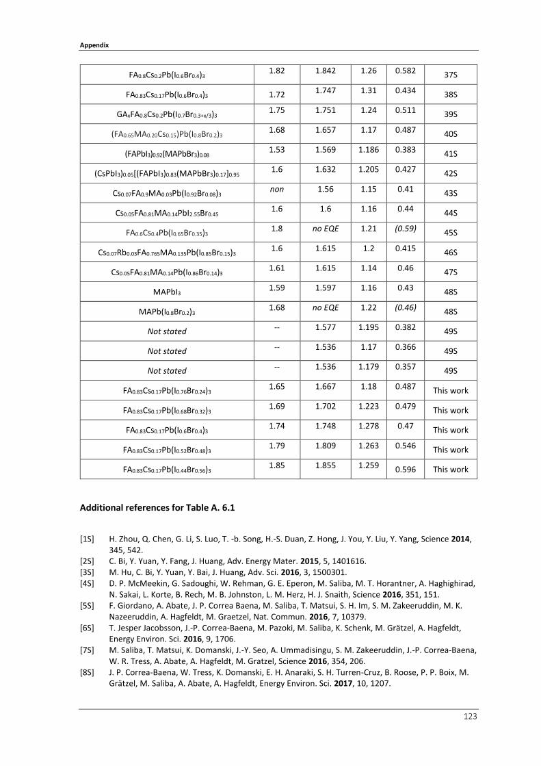
Appendix
123
FA0.8Cs0.2Pb(I0.6Br0.4)3 1.82 1.842 1.26 0.582 37S
FA0.83Cs0.17Pb(I0.6Br0.4)3 1.72 1.747 1.31 0.434 38S
GAxFA0.8Cs0.2Pb(I0.7Br0.3+x/3)3 1.75 1.751 1.24 0.511 39S
(FA0.65MA0.20Cs0.15)Pb(I0.8Br0.2)3 1.68 1.657 1.17 0.487 40S
(FAPbI3)0.92(MAPbBr3)0.08 1.53 1.569 1.186 0.383 41S
(CsPbI3)0.05[(FAPbI3)0.83(MAPbBr3)0.17]0.95 1.6 1.632 1.205 0.427 42S
Cs0.07FA0.9MA0.03Pb(I0.92Br0.08)3 non 1.56 1.15 0.41 43S
Cs0.05FA0.81MA0.14PbI2.55Br0.45 1.6 1.6 1.16 0.44 44S
FA0.6Cs0.4Pb(I0.65Br0.35)3 1.8 no EQE 1.21 (0.59) 45S
Cs0.07Rb0.03FA0.765MA0.135Pb(I0.85Br0.15)3 1.6 1.615 1.2 0.415 46S
Cs0.05FA0.81MA0.14Pb(I0.86Br0.14)3 1.61 1.615 1.14 0.46 47S
MAPbI3 1.59 1.597 1.16 0.43 48S
MAPb(I0.8Br0.2)3 1.68 no EQE 1.22 (0.46) 48S
Not stated -- 1.577 1.195 0.382 49S
Not stated -- 1.536 1.17 0.366 49S
Not stated -- 1.536 1.179 0.357 49S
FA0.83Cs0.17Pb(I0.76Br0.24)3 1.65 1.667 1.18 0.487 This work
FA0.83Cs0.17Pb(I0.68Br0.32)3 1.69 1.702 1.223 0.479 This work
FA0.83Cs0.17Pb(I0.6Br0.4)3 1.74 1.748 1.278 0.47 This work
FA0.83Cs0.17Pb(I0.52Br0.48)3 1.79 1.809 1.263 0.546 This work
FA0.83Cs0.17Pb(I0.44Br0.56)3 1.85 1.855 1.259 0.596 This work
Additional references for Table A. 6.1
[1S] H. Zhou, Q. Chen, G. Li, S. Luo, T. -b. Song, H.-S. Duan, Z. Hong, J. You, Y. Liu, Y. Yang, Science 2014, 345, 542.
[2S] C. Bi, Y. Yuan, Y. Fang, J. Huang, Adv. Energy Mater. 2015, 5, 1401616. [3S] M. Hu, C. Bi, Y. Yuan, Y. Bai, J. Huang, Adv. Sci. 2016, 3, 1500301. [4S] D. P. McMeekin, G. Sadoughi, W. Rehman, G. E. Eperon, M. Saliba, M. T. Horantner, A. Haghighirad,
N. Sakai, L. Korte, B. Rech, M. B. Johnston, L. M. Herz, H. J. Snaith, Science 2016, 351, 151. [5S] F. Giordano, A. Abate, J. P. Correa Baena, M. Saliba, T. Matsui, S. H. Im, S. M. Zakeeruddin, M. K.
Nazeeruddin, A. Hagfeldt, M. Graetzel, Nat. Commun. 2016, 7, 10379. [6S] T. Jesper Jacobsson, J.-P. Correa-Baena, M. Pazoki, M. Saliba, K. Schenk, M. Grätzel, A. Hagfeldt,
Energy Environ. Sci. 2016, 9, 1706. [7S] M. Saliba, T. Matsui, K. Domanski, J.-Y. Seo, A. Ummadisingu, S. M. Zakeeruddin, J.-P. Correa-Baena,
W. R. Tress, A. Abate, A. Hagfeldt, M. Gratzel, Science 2016, 354, 206. [8S] J. P. Correa-Baena, W. Tress, K. Domanski, E. H. Anaraki, S. H. Turren-Cruz, B. Roose, P. P. Boix, M.
Grätzel, M. Saliba, A. Abate, A. Hagfeldt, Energy Environ. Sci. 2017, 10, 1207.

Appendix
124
[9S] T. Duong, Y. Wu, H. Shen, J. Peng, X. Fu, D. Jacobs, E.-C. Wang, T. C. Kho, K. C. Fong, M. Stocks, E. Franklin, A. Blakers, N. Zin, K. McIntosh, W. Li, Y.-B. Cheng, T. P. White, K. Weber, K. Catchpole, Adv. Energy Mater. 2017, 7, 1700228.
[10S] Y. Yu, C. Wang, C. R. Grice, N. Shrestha, D. Zhao, W. Liao, L. Guan, R. A. Awni, W. Meng, A. J. Cimaroli, K. Zhu, R. J. Ellingson, Y. Yan, ACS Energy Lett. 2017, 2, 1177.
[11S] Y. Lin, B. Chen, F. Zhao, X. Zheng, Y. Deng, Y. Shao, Y. Fang, Y. Bai, C. Wang, J. Huang, Adv. Mater. 2017, 29, 1700607.
[12S] Y. Bai, S. Xiao, C. Hu, T. Zhang, X. Meng, H. Lin, Y. Yang, S. Yang, Adv. Energy Mater. 2017, 7, 1701038.
[13S] J. Peng, Y. Wu, W. Ye, D. A. Jacobs, H. Shen, X. Fu, Y. Wan, T. Duong, N. Wu, C. Barugkin, H. T. Nguyen, D. Zhong, J. Li, T. Lu, Y. Liu, M. N. Lockrey, K. J. Weber, K. R. Catchpole, T. P. White, Energy Environ. Sci. 2017, 10, 1792.
[14S] X. Zheng, B. Chen, J. Dai, Y. Fang, Y. Bai, Y. Lin, H. Wei, X. C. Zeng, J. Huang, Nat. Energy 2017, 2, 17102.
[15S] Z. Wang, Q. Lin, F. P. Chmiel, N. Sakai, L. M. Herz, H. J. Snaith, Nat. Energy 2017, 2, 17135. [16S] Y. Zhou, F. Wang, Y. Cao, J.-P. Wang, H.-H. Fang, M. A. Loi, N. Zhao, C.-P. Wong, Adv. Energy Mater.
2017, 7, 1701048. [17S] G. Longo, C. Momblona, M.-G. La-Placa, L. Gil-Escrig, M. Sessolo, H. J. Bolink, ACS Energy Lett. 2018,
3, 214. [18S] D. Zhao, C. Wang, Z. Song, Y. Yu, C. Chen, X. Zhao, K. Zhu, Y. Yan, ACS Energy Lett. 2018, 3, 305. [19S] K. A. Bush, K. Frohna, R. Prasanna, R. E. Beal, T. Leijtens, S. A. Swifter, M. D. McGehee, ACS Energy
Lett. 2018, 3, 428. [20S] K. T. Cho, G. Grancini, Y. Lee, E. Oveisi, J. Ryu, O. Almora, M. Tschumi, P. A. Schouwink, G. Seo, S.
Heo, J. Park, J. Jang, S. Paek, G. Garcia-Belmonte, M. K. Nazeeruddin, Energy Environ. Sci. 2018, 11, 952.
[21S] J. Kim, M. I. Saidaminov, H. Tan, Y. Zhao, Y. Kim, J. Choi, J. W. Jo, J. Fan, R. Quintero-Bermudez, Z. Yang, L. N. Quan, M. Wei, O. Voznyy, E. H. Sargent, Adv. Mater. 2018, 30, 1706275.
[22S] M. Abdi-Jalebi, Z. Andaji-Garmaroudi, S. Cacovich, C. Stavrakas, B. Philippe, J. M. Richter, M. Alsari, E. P. Booker, E. M. Hutter, A. J. Pearson, S. Lilliu, T. J. Savenije, H. Rensmo, G. Divitini, C. Ducati, R. H. Friend, S. D. Stranks, Nature 2018, 555, 497.
[23S] A. Rajagopal, R. J. Stoddard, S. B. Jo, H. W. Hillhouse, A. K. Y. Jen, Nano Lett. 2018, 18, 3985. [24S] D. B. Khadka, Y. Shirai, M. Yanagida, T. Noda, K. Miyano, ACS Appl. Mater. Interfaces 2018, 10,
22074. [25S] D. Luo, W. Yang, Z. Wang, A. Sadhanala, Q. Hu, R. Su, R. Shivanna, G. F. Trindade, J. F. Watts, Z. Xu,
T. Liu, K. Chen, F. Ye, P. Wu, L. Zhao, J. Wu, Y. Tu, Y. Zhang, X. Yang, W. Zhang, R. H. Friend, Q. Gong, H. J. Snaith, R. Zhu, Science 2018, 360, 1442.
[26S] Y. Zhou, Y.-H. Jia, H.-H. Fang, M. A. Loi, F.-Y. Xie, L. Gong, M.-C. Qin, X.-H. Lu, C.-P. Wong, N. Zhao, Adv. Funct. Mater. 2018, 28, 1803130.
[27S] H. Tan, F. Che, M. Wei, Y. Zhao, M. I. Saidaminov, P. Todorović, D. Broberg, G. Walters, F. Tan, T. Zhuang, B. Sun, Z. Liang, H. Yuan, E. Fron, J. Kim, Z. Yang, O. Voznyy, M. Asta, E. H. Sargent, Nat. Commun. 2018, 9, 3100.
[28S] M. M. Tavakoli, W. Tress, J. V. Milić, D. Kubicki, L. Emsley, M. Grätzel, Energy Environ. Sci. 2018, 11, 3310.
[29S] S. Chen, Y. Hou, H. Chen, X. Tang, S. Langner, N. Li, T. Stubhan, I. Levchuk, E. Gu, A. Osvet, C. J. Brabec, Adv. Energy Mater. 2018, 8, 1701543.
[30S] Z. Liu, L. Krückemeier, B. Krogmeier, B. Klingebiel, J. A. Márquez, S. Levcenko, S. Öz, S. Mathur, U. Rau, T. Unold, T. Kirchartz, ACS Energy Lett. 2019, 4, 110.
[31S] M. Jaysankar, B. A. L. Raul, J. Bastos, C. Burgess, C. Weijtens, M. Creatore, T. Aernouts, Y. Kuang, R. Gehlhaar, A. Hadipour, J. Poortmans, ACS Energy Lett. 2019, 4, 259.
[32S] P. Guo, Q. Ye, X. Yang, J. Zhang, F. Xu, D. Shchukin, B. Wei, H. Wang, J. Mater. Chem. A 2019, 7, 2497.
[33S] D. Prochowicz, R. Runjhun, M. M. Tavakoli, P. Yadav, M. Saski, A. Q. Alanazi, D. J. Kubicki, Z. Kaszkur, S. M. Zakeeruddin, J. Lewiński, M. Grätzel, Chem. Mater. 2019, 31, 1620.
[34S] D. Prochowicz, M. M. Tavakoli, A. Kalam, R. D. Chavan, S. Trivedi, M. Kumar, P. Yadav, J. Mater. Chem. A 2019, 7, 8218.
[35S] Y. Chen, N. Li, L. Wang, L. Li, Z. Xu, H. Jiao, P. Liu, C. Zhu, H. Zai, M. Sun, W. Zou, S. Zhang, G. Xing, X. Liu, J. Wang, D. Li, B. Huang, Q. Chen, H. Zhou, Nat. Commun. 2019, 10, 1112.

Appendix
125
[36S] S. Yang, J. Dai, Z. Yu, Y. Shao, Y. Zhou, X. Xiao, X. C. Zeng, J. Huang, J. Am. Chem. Soc. 2019, 141, 5781.
[37S] W.-Q. Wu, Z. Yang, P. N. Rudd, Y. Shao, X. Dai, H. Wei, J. Zhao, Y. Fang, Q. Wang, Y. Liu, Y. Deng, X. Xiao, Y. Feng, J. Huang, Sci. Adv. 2019, 5, eaav8925.
[38S] S. Gharibzadeh, B. Abdollahi Nejand, M. Jakoby, T. Abzieher, D. Hauschild, S. Moghadamzadeh, J. A. Schwenzer, P. Brenner, R. Schmager, A. A. Haghighirad, L. Weinhardt, U. Lemmer, B. S. Richards, I. A. Howard, U. W. Paetzold, Adv. Energy Mater. 2019, 9, 1803699.
[39S] C. Chen, Z. Song, C. Xiao, D. Zhao, N. Shrestha, C. Li, G. Yang, F. Yao, X. Zheng, R. J. Ellingson, C.-S. Jiang, M. Al-Jassim, K. Zhu, G. Fang, Y. Yan, Nano Energy 2019, 61, 141.
[40S] D. H. Kim, C. P. Muzzillo, J. Tong, A. F. Palmstrom, B. W. Larson, C. Choi, S. P. Harvey, S. Glynn, J. B. Whitaker, F. Zhang, Z. Li, H. Lu, M. F. A. M. van Hest, J. J. Berry, L. M. Mansfield, Y. Huang, Y. Yan, K. Zhu, Joule 2019, 3, 1734.
[41S] J. J. Yoo, S. Wieghold, M. C. Sponseller, M. R. Chua, S. N. Bertram, N. T. P. Hartono, J. S. Tresback, E. C. Hansen, J.-P. Correa-Baena, V. Bulović, T. Buonassisi, S. S. Shin, M. G. Bawendi, Energy Environ. Sci. 2019, 12, 2192.
[42S] M. Stolterfoht, P. Caprioglio, C. M. Wolff, J. A. Márquez, J. Nordmann, S. Zhang, D. Rothhardt, U. Hörmann, Y. Amir, A. Redinger, L. Kegelmann, F. Zu, S. Albrecht, N. Koch, T. Kirchartz, M. Saliba, T. Unold, D. Neher, Energy Environ. Sci. 2019, 12, 2778.
[43S] E. A. Alharbi, A. Y. Alyamani, D. J. Kubicki, A. R. Uhl, B. J. Walder, A. Q. Alanazi, J. Luo, A. Burgos-Caminal, A. Albadri, H. Albrithen, M. H. Alotaibi, J.-E. Moser, S. M. Zakeeruddin, F. Giordano, L. Emsley, M. Grätzel, Nat. Commun. 2019, 10, 3008.
[44S] S. Yang, S. Chen, E. Mosconi, Y. Fang, X. Xiao, C. Wang, Y. Zhou, Z. Yu, J. Zhao, Y. Gao, F. De Angelis, J. Huang, Science 2019, 365, 473.
[45S] Z. Yang, Z. Yu, H. Wei, X. Xiao, Z. Ni, B. Chen, Y. Deng, S. N. Habisreutinger, X. Chen, K. Wang, J. Zhao, P. N. Rudd, J. J. Berry, M. C. Beard, J. Huang, Nat. Commun. 2019, 10, 4498.
[46S] M. A. Mahmud, T. Duong, Y. Yin, H. T. Pham, D. Walter, J. Peng, Y. Wu, L. Li, H. Shen, N. Wu, N. Mozaffari, G. Andersson, K. R. Catchpole, K. J. Weber, T. P. White, Adv. Funct. Mater. 2019, doi: 10.1002/adfm.201907962.
[47S] Y. Lv, X. Song, Y. Yin, Y. Feng, H. Ma, C. Hao, S. Jin, Y. Shi, ACS Appl. Mater. Interfaces 2020, 12, 698. [48S] C.-T. Lin, J. Lee, J. Kim, T. J. Macdonald, J. Ngiam, B. Xu, M. Daboczi, W. Xu, S. Pont, B. Park, H. Kang,
J.-S. Kim, D. J. Payne, K. Lee, J. R. Durrant, M. A. McLachlan, Adv. Funct. Mater. 2019, 1906763, 1906763.
[49S] M. A. Green, A. W. Y. Ho-Baillie, ACS Energy Lett. 2019, 4, 1639.

126
References
1. Masson-Delmotte, V. et al. IPCC, 2018: Global Warming of 1.5°C. https://www.ipcc.ch/site/assets/uploads/sites/2/2019/06/SR15_Full_Report_High_Res.pdf (2019) doi:10.1038/291285a0.
2. Nukunudompanich, M., Budiutama, G., Suzuki, K., Hasegawa, K. & Ihara, M. Dominant effect of the grain size of the MAPbI 3 perovskite controlled by the surface roughness of TiO 2 on the performance of perovskite solar cells . CrystEngComm (2020) doi:10.1039/d0ce00169d.
3. Heede, R. & Oreskes, N. Potential emissions of CO2 and methane from proved reserves of fossil fuels: An alternative analysis. Glob. Environ. Chang. 36, 12–20 (2016).
4. Michael Oppenheimer. Global warming and the stability of the West Antarctic Ice Sheet. Nature 393, 325–332 (1998).
5. Dobson, A., Jolly, A., Rubenstein, D. & Woodwell, G. The Greenhouse Effect and Biological Diversity. Tree 4, 64–68 (1989).
6. UNFCCC. Conference of the Parties, Paris Agreement 2015. doi:FCCC/CP/2015/L.9/Rev.1.
7. IEA, World Energy Outlook 2019, Paris. https://www.iea.org/reports/world-energy-outlook-2019 (2019).
8. Kost, C. et al. Fraunhofer ISE: Levelized Cost of Electricity - Renewable Energy Technologies, March 2018. Fraunhofer ISE: Levelized Cost of Electricity - Renewable Energy Technologies (2018).
9. Howard, I. A. et al. Coated and Printed Perovskites for Photovoltaic Applications. Adv. Mater. 31, 1806702 (2019).
10. NREL. National Renewable Energy Laboratory (NREL), Efficiency chart, 2020. https://www.nrel.gov/pv/cell-efficiency.html (2020).
11. Hwang, K. et al. Toward large scale roll-to-roll production of fully printed perovskite solar cells. Adv. Mater. 27, 1241–1247 (2015).
12. Albrecht, S. & Rech, B. Perovskite solar cells: On top of commercial photovoltaics. Nat. Energy 2, 16196 (2017).
13. Duong, T. et al. High Efficiency Perovskite-Silicon Tandem Solar Cells: Effect of Surface Coating versus Bulk Incorporation of 2D Perovskite. Adv. Energy Mater. 10, 1–15 (2020).
14. Chen, B. et al. Enhanced optical path and electron diffusion length enable high-efficiency perovskite tandems. Nat. Commun. 11, (2020).

References
127
15. Jacobs, D. A. et al. Light Management: A Key Concept in High-Efficiency Perovskite/Silicon Tandem Photovoltaics. J. Phys. Chem. Lett. 10, 3159–3170 (2019).
16. Duong, T. et al. Semitransparent Perovskite Solar Cell With Sputtered Front and Rear Electrodes for a Four-Terminal Tandem. IEEE J. Photovoltaics 6, 679–687 (2016).
17. Eperon, G. E., Hörantner, M. T. & Snaith, H. J. Metal halide perovskite tandem and multiple-junction photovoltaics. Nat. Rev. Chem. 1, (2017).
18. Futscher, M. H. & Ehrler, B. Efficiency Limit of Perovskite/Si Tandem Solar Cells. ACS Energy Lett. 1, 863–868 (2016).
19. Hoke, E. T. et al. Reversible photo-induced trap formation in mixed-halide hybrid perovskites for photovoltaics. Chem. Sci. 6, 613–617 (2015).
20. Levine, I. et al. Deep Defect States in Wide-Band-Gap ABX 3 Halide Perovskites. ACS Energy Lett. 4, 1150–1157 (2019).
21. Tan, H. et al. Dipolar cations confer defect tolerance in wide-bandgap metal halide perovskites. Nat. Commun. 9, 3100 (2018).
22. Lin, Y. et al. Matching Charge Extraction Contact for Wide-Bandgap Perovskite Solar Cells. Adv. Mater. 29, 1700607 (2017).
23. Belisle, R. A. et al. Impact of surfaces on photoinduced halide segregation in mixed-halide perovskites. ACS Energy Lett. 3, 2694–2700 (2018).
24. Jaysankar, M. et al. Minimizing Voltage Loss in Wide-Bandgap Perovskites for Tandem Solar Cells. ACS Energy Lett. 4, 259–264 (2019).
25. Bush, K. A. et al. Compositional Engineering for Efficient Wide Band Gap Perovskites with Improved Stability to Photoinduced Phase Segregation. ACS Energy Lett. 3, 428–435 (2018).
26. Unger, E. L. et al. Roadmap and roadblocks for the band gap tunability of metal halide perovskites. J. Mater. Chem. A 5, 11401–11409 (2017).
27. Yang, T. C. J., Fiala, P., Jeangros, Q. & Ballif, C. High-Bandgap Perovskite Materials for Multijunction Solar Cells. Joule 2, 1421–1436 (2018).
28. Mahmood, K., Sarwar, S. & Mehran, M. T. Current status of electron transport layers in perovskite solar cells: materials and properties. RSC Adv. 7, 17044–17062 (2017).
29. Wu, W.-Q., Chen, D., Caruso, R. A. & Cheng, Y.-B. Recent progress in hybrid perovskite solar cells based on n-type materials. J. Mater. Chem. A 5, 10092–10109 (2017).

References
128
30. Yang, G., Tao, H., Qin, P., Ke, W. & Fang, G. Recent progress in electron transport layers for e ffi cient perovskite solar cells. J. Mater. Chem. A Mater. energy Sustain. 4, 3970–3990 (2016).
31. Yang, W. S. et al. Iodide management in formamidinium-lead-halide–based perovskite layers for efficient solar cells. Science 356, 1376–1379 (2017).
32. Saliba, M. et al. Cesium-containing triple cation perovskite solar cells: improved stability, reproducibility and high efficiency. Energy Environ. Sci. 9, 1989–1997 (2016).
33. Saliba, M. et al. Incorporation of rubidium cations into perovskite solar cells improves photovoltaic performance. Science 354, 206–209 (2016).
34. Duong, T. et al. Rubidium Multication Perovskite with Optimized Bandgap for Perovskite-Silicon Tandem with over 26% Efficiency. Adv. Energy Mater. 7, 1700228 (2017).
35. Kim, H. S. & Park, N. G. Parameters affecting I-V hysteresis of CH3NH3PbI3 perovskite solar cells: Effects of perovskite crystal size and mesoporous TiO2 layer. J. Phys. Chem. Lett. 5, 2927–2934 (2014).
36. Schultes, M. et al. Sputtered Transparent Electrodes (IO:H and IZO) with Low Parasitic Near-Infrared Absorption for Perovskite-Cu(In,Ga)Se2 Tandem Solar Cells. ACS Appl. Energy Mater. 2, 7823–7831 (2019).
37. Schultes, M. Four – Terminal Perovskite – CIGS Tandem Solar Cells with Improved Near – Infrared Response. (2019).
38. Jaysankar, M. et al. Perovskite-silicon tandem solar modules with optimised light harvesting. Energy Environ. Sci. 11, 1489–1498 (2018).
39. Brewer, S. H. & Franzen, S. Indium tin oxide plasma frequency dependence on sheet resistance and surface adlayers determined by reflectance FTIR spectroscopy. J. Phys. Chem. B 106, 12986–12992 (2002).
40. Sathiaraj, T. S. Effect of annealing on the structural, optical and electrical properties of ITO films by RF sputtering under low vacuum level. Microelectronics J. 39, 1444–1451 (2008).
41. Paetzold, U. W., Qiu, W., Finger, F., Poortmans, J. & Cheyns, D. Nanophotonic front electrodes for perovskite solar cells. Appl. Phys. Lett. 106, (2015).
42. Chen, D. et al. Nanophotonic Light Management for Perovskite-Silicon Tandem Solar Cells. 1–14 (2018) doi:10.1117/1.JPE.8.022601.
43. Tockhorn, P. et al. Improved Quantum Efficiency by Advanced Light Management in Nanotextured Solution-Processed Perovskite Solar Cells. ACS Photonics 7, 2589–2600 (2020).

References
129
44. Langenhorst, M. et al. Energy yield of all thin-film perovskite/CIGS tandem solar modules. Prog. Photovoltaics Res. Appl. 290–298 (2018) doi:10.1002/pip.3091.
45. Kim, D. H. et al. Bimolecular Additives Improve Wide-Band-Gap Perovskites for Efficient Tandem Solar Cells with CIGS. Joule 3, 1734–1745 (2019).
46. Scharber, M. C. & Sariciftci, N. S. Efficiency of bulk-heterojunction organic solar cells. Prog. Polym. Sci. 38, 1929–1940 (2013).
47. Carlson, D. E. & Wronski, C. R. Amorphous silicon solar cell. Appl. Phys. Lett. 28, 671–673 (1976).
48. Kojima, A., Teshima, K., Shirai, Y. & Miyasaka, T. Organometal halide perovskites as visible-light sensitizers for photovoltaic cells. J. Am. Chem. Soc. 131, 6050–6051 (2009).
49. Kasap, S. O. Principles of Electronic Materials and Devices. (Tata McGraw-Hill, 2006).
50. Stranks, S. D. et al. Electron-hole diffusion lengths exceeding 1 micrometer in an organometal trihalide perovskite absorber. Science 342, 341–344 (2013).
51. Hellmann, T. et al. The difference in electronic structure of MAPI and MASI perovskites and its effect on the interface alignment to the HTMs spiro-MeOTAD and CuI. J. Mater. Chem. C 7, 5324–5332 (2019).
52. Byeon, J. et al. Charge transport layer dependent electronic band bending in perovskite solar cells and its correlation to device degradation. arXiv (2019).
53. Wurfel, U., Cuevas, A. & Wurfel, P. Charge carrier separation in solar cells. IEEE J. Photovoltaics 5, 461–469 (2015).
54. NREL. AM 1.5G spectrum. https://www.nrel.gov/grid/solar-resource/spectra-am1.5.html.
55. Rau, U., Paetzold, U. W. & Kirchartz, T. Thermodynamics of light management in photovoltaic devices. Phys. Rev. B - Condens. Matter Mater. Phys. 90, 1–16 (2014).
56. Mäckel, H. & Cuevas, A. Determination of the surface recombination velocity of unpassivated silicon from spectral photoconductance measurements. Proc. 3rd World Conf. Photovolt. Energy Convers. A, 71–74 (2003).
57. Köhler, A. & Bässler, H. Electronic Processes in Organic Semiconductors. (Wiley-VCH, 2015).
58. Shen, H. et al. Mechanically-stacked perovskite/CIGS tandem solar cells with efficiency of 23.9% and reduced oxygen sensitivity. Energy Environ. Sci. 11, 394–406 (2018).
59. Deinega, A., Valuev, I., Potapkin, B. & Lozovik, Y. Minimizing light reflection from

References
130
dielectric textured surfaces. J. Opt. Soc. Am. A 28, 770 (2011).
60. Schneider, B. W., Lal, N. N., Baker-Finch, S. & White, T. P. Pyramidal surface textures for light trapping and antireflection in perovskite-on-silicon tandem solar cells. Opt. Express 22, A1422 (2014).
61. Schmager, R. et al. Texture of the Viola Flower for Light Harvesting in Photovoltaics. ACS Photonics 4, 2687–2692 (2017).
62. Dottermusch, S. et al. Micro-cone textures for improved light in-coupling and retroreflection-inspired light trapping at the front surface of solar modules. Prog. Photovoltaics Res. Appl. 27, 593–602 (2019).
63. Jošt, M. et al. Textured interfaces in monolithic perovskite/silicon tandem solar cells: Advanced light management for improved efficiency and energy yield. Energy Environ. Sci. 11, 3511–3523 (2018).
64. Wei, J. et al. Enhanced Light Harvesting in Perovskite Solar Cells by a Bioinspired Nanostructured Back Electrode. Adv. Energy Mater. 7, 1–7 (2017).
65. Zhang, H., Kramarenko, M., Osmond, J., Toudert, J. & Martorell, J. Natural Random Nanotexturing of the Au Interface for Light Backscattering Enhanced Performance in Perovskite Solar Cells. ACS Photonics 5, 2243–2250 (2018).
66. Yablonovitch, E. Statistical Ray Optics. J. Opt. Soc. Am. 72, 899–907 (1982).
67. Yablonovitch, E. & Cody, G. D. Intensity enhancement in textured optical sheets for solar cells. IEEE Trans. Electron Devices 2, 300 (1982).
68. Yu, Z., Raman, A. & Fan, S. Fundamental limit of nanophotonic light trapping in solar cells. Proc. Natl. Acad. Sci. U. S. A. 107, 17491–17496 (2010).
69. Schmager, R., Gomard, G., Richards, B. S. & Paetzold, U. W. Nanophotonic perovskite layers for enhanced current generation and mitigation of lead in perovskite solar cells. Sol. Energy Mater. Sol. Cells 192, 65–71 (2019).
70. Jiang, Q. et al. Enhanced electron extraction using SnO2 for high-efficiency planar-structure HC(NH2)2 PbI3-based perovskite solar cells. Nat. Energy 2, (2017).
71. Hossain, I. M. et al. Nanostructured front electrodes for perovskite/c-Si tandem photovoltaics. Opt. Express 28, 8878 (2020).
72. Khan, I., Bauch, M., Dimopoulos, T. & Dostalek, J. Nanostructured as-deposited indium tin oxide thin films for broadband antireflection and light trapping. Nanotechnology 28, 325201 (2017).
73. Shockley, W. & Queisser, H. J. Detailed balance limit of efficiency of p-n junction solar cells. J. Appl. Phys. 32, 510–519 (1961).
74. Bremner, S. P., Levy, M. Y. & Honsberg, C. B. Analysis of tandem solar cell

References
131
efficiencies under AM1.5G spectrum using a rapid flux calculation method. Prog. Photovoltaics Res. Appl. 16, 225–233 (2008).
75. Vos, a De, De Vos, A. & Vos, a De. Detailed balance limit of the efficiency of tandem solar cells. J. Phys. D. Appl. Phys. 13, 839–846 (1980).
76. Schmager, R. et al. Methodology of energy yield modelling of perovskite-based multi-junction photovoltaics. Opt. Express 27, A507 (2019).
77. Lehr, J. et al. Energy yield modelling of perovskite/silicon two-terminal tandem PV modules with flat and textured interfaces. Sustain. Energy Fuels 2, 2754–2761 (2018).
78. Lal, N. N. et al. Perovskite Tandem Solar Cells. Adv. Energy Mater. 1602761, 1–18 (2017).
79. Sahli, F. et al. Fully textured monolithic perovskite/silicon tandem solar cells with 25.2% power conversion efficiency. Nat. Mater. 17, 820–826 (2018).
80. Al-Ashouri, A. et al. Conformal monolayer contacts with lossless interfaces for perovskite single junction and monolithic tandem solar cells. Energy Environ. Sci. 12, 3356–3369 (2019).
81. Eperon, G. E. et al. Perovskite-perovskite tandem photovoltaics with optimized band gaps. Science (80-. ). 354, 861–865 (2016).
82. Abdollahi Nejand, B. et al. Vacuum-Assisted Growth of Low-Bandgap Thin Films (FA0.8MA0.2Sn0.5Pb0.5I3) for All-Perovskite Tandem Solar Cells. Adv. Energy Mater. 10, (2020).
83. Eperon, G. E. et al. Formamidinium lead trihalide: A broadly tunable perovskite for efficient planar heterojunction solar cells. Energy Environ. Sci. 7, 982–988 (2014).
84. Brenner, P. et al. Triple cation mixed-halide perovskites for tunable lasers. Opt. Mater. Express 7, 4082 (2017).
85. Bailie, C. D. et al. Semi-transparent perovskite solar cells for tandems with silicon and CIGS. Energy Environ. Sci. 8, 956–963 (2015).
86. Whitfield, P. S. et al. Structures, Phase Transitions and Tricritical Behavior of the Hybrid Perovskite Methyl Ammonium Lead Iodide. Sci. Rep. 6, 1–16 (2016).
87. Baikie, T. et al. Synthesis and crystal chemistry of the hybrid perovskite (CH 3NH3)PbI3 for solid-state sensitised solar cell applications. J. Mater. Chem. A 1, 5628–5641 (2013).
88. Goldschmidt, V. M. et al. Krystallbau und chemische Zusammensetzun. (1927).
89. Farooq, A. et al. Spectral Dependence of Degradation under Ultraviolet Light in Perovskite Solar Cells. ACS Appl. Mater. Interfaces 10, 21985–21990 (2018).
References
132
90. Chen, Y. et al. 2D Ruddlesden–Popper Perovskites for Optoelectronics. Adv. Mater. 30, 1–15 (2018).
91. Gharibzadeh, S. et al. Record Open-Circuit Voltage Wide-Bandgap Perovskite Solar Cells Utilizing 2D/3D Perovskite Heterostructure. Adv. Energy Mater. 9, 1–10 (2019).
92. Ahmad, S. et al. Dion-Jacobson Phase 2D Layered Perovskites for Solar Cells with Ultrahigh Stability. Joule 3, 794–806 (2019).
93. Lee, J. W. et al. 2D perovskite stabilized phase-pure formamidinium perovskite solar cells. Nat. Commun. 9, 1–10 (2018).
94. Koh, T. M. et al. Enhancing moisture tolerance in efficient hybrid 3D/2D perovskite photovoltaics. J. Mater. Chem. A 6, 2122–2128 (2018).
95. Liu, G. et al. Introduction of Hydrophobic Ammonium Salts with Halogen Functional Groups for High-Efficiency and Stable 2D/3D Perovskite Solar Cells. Adv. Funct. Mater. 29, 1–9 (2019).
96. De Wolf, S. et al. Organometallic halide perovskites: Sharp optical absorption edge and its relation to photovoltaic performance. J. Phys. Chem. Lett. 5, 1035–1039 (2014).
97. Wehrenfennig, C., Eperon, G. E., Johnston, M. B., Snaith, H. J. & Herz, L. M. High charge carrier mobilities and lifetimes in organolead trihalide perovskites. Adv. Mater. 26, 1584–1589 (2014).
98. McMeekin, D. P. et al. A mixed-cation lead mixed-halide perovskite absorber for tandem solar cells. Science (80-. ). 351, 151–155 (2016).
99. Gharibzadeh, S. et al. 2D/3D Heterostructure for Semitransparent Perovskite Solar Cells with Engineered Bandgap Enables Efficiencies Exceeding 25% in Four-Terminal Tandems with Silicon and CIGS. Adv. Funct. Mater. (2020) doi:10.1002/adfm.201909919.
100. Kumawat, N. K., Liu, X. K., Kabra, D. & Gao, F. Blue perovskite light-emitting diodes: Progress, challenges and future directions. Nanoscale 11, 2109–2120 (2019).
101. Mali, S. S. & Hong, C. K. P-i-n/n-i-p type planar hybrid structure of highly efficient perovskite solar cells towards improved air stability: Synthetic strategies and the role of p-type hole transport layer (HTL) and n-type electron transport layer (ETL) metal oxides. Nanoscale 8, 10528–10540 (2016).
102. Yang, G., Tao, H., Qin, P., Ke, W. & Fang, G. Recent progress in electron transport layers for efficient perovskite solar cells. J. Mater. Chem. A 4, 3970–3990 (2016).
103. Chueh, C. C., Li, C. Z. & Jen, A. K. Y. Recent progress and perspective in solution-processed Interfacial materials for efficient and stable polymer and organometal

References
133
perovskite solar cells. Energy Environ. Sci. 8, 1160–1189 (2015).
104. Xiong, L. et al. Review on the Application of SnO2 in Perovskite Solar Cells. Adv. Funct. Mater. 28, 1–18 (2018).
105. Hu, Z. et al. Effects of heteroatom substitution in spiro-bifluorene hole transport materials. Chem. Sci. 7, 5007–5012 (2016).
106. Saliba, M. et al. How to Make over 20% Efficient Perovskite Solar Cells in Regular (n-i-p) and Inverted (p-i-n) Architectures. Chem. Mater. 30, 4193–4201 (2018).
107. Wu, C.-G. et al. High efficiency stable inverted perovskite solar cells without current hysteresis. Energy Environ. Sci. 8, 2725–2733 (2015).
108. Abzieher, T. et al. Electron‐Beam‐Evaporated Nickel Oxide Hole Transport Layers for Perovskite‐Based Photovoltaics. Adv. Energy Mater. 9, 1802995 (2019).
109. Bastos, J. P. et al. Low-cost electrodes for stable perovskite solar cells. Appl. Phys. Lett. 110, (2017).
110. Li, L. et al. The Additive Coordination Effect on Hybrids Perovskite Crystallization and High-Performance Solar Cell. Adv. Mater. 28, 9862–9868 (2016).
111. Zheng, X. et al. Defect passivation in hybrid perovskite solar cells using quaternary ammonium halide anions and cations. Nat. Energy 2, 1–9 (2017).
112. Yin, W. J., Shi, T. & Yan, Y. Unusual defect physics in CH3NH3PbI3 perovskite solar cell absorber. Appl. Phys. Lett. 104, (2014).
113. Aranda, C., Guerrero, A. & Bisquert, J. Ionic Effect Enhances Light Emission and the Photovoltage of Methylammonium Lead Bromide Perovskite Solar Cells by Reduced Surface Recombination. ACS Energy Lett. 4, 741–746 (2019).
114. Yang, D. et al. Stable Efficiency Exceeding 20.6% for Inverted Perovskite Solar Cells through Polymer-Optimized PCBM Electron-Transport Layers. Nano Lett. 19, 3313–3320 (2019).
115. Abdi-Jalebi, M. et al. Charge extraction via graded doping of hole transport layers gives highly luminescent and stable metal halide perovskite devices. Sci. Adv. 5, 1–10 (2019).
116. Halvani Anaraki, E. et al. Low-Temperature Nb-Doped SnO2 Electron-Selective Contact Yields over 20% Efficiency in Planar Perovskite Solar Cells. ACS Energy Lett. 3, 773–778 (2018).
117. Arora, N. et al. Perovskite solar cells with CuSCN hole extraction layers yield stabilized efficiencies greater than 20 %. 5655, 1–9 (2017).
118. Snaith, H. J. et al. Anomalous hysteresis in perovskite solar cells. J. Phys. Chem. Lett. 5, 1511–1515 (2014).

References
134
119. Van Reenen, S., Kemerink, M. & Snaith, H. J. Modeling Anomalous Hysteresis in Perovskite Solar Cells. J. Phys. Chem. Lett. 6, 3808–3814 (2015).
120. Hermes, I. M., Hou, Y., Bergmann, V. W., Brabec, C. J. & Weber, S. A. L. The Interplay of Contact Layers: How the Electron Transport Layer Influences Interfacial Recombination and Hole Extraction in Perovskite Solar Cells. J. Phys. Chem. Lett. 9, 6249–6256 (2018).
121. Christians, J. A., Manser, J. S. & Kamat, P. V. Best practices in perovskite solar cell efficiency measurements. Avoiding the error of Making Bad Cells Look Good. J. Phys. Chem. Lett. 6, 852–857 (2015).
122. Khenkin, M. V. et al. Consensus statement for stability assessment and reporting for perovskite photovoltaics based on ISOS procedures. Nat. Energy 5, 35–49 (2020).
123. Wang, R. et al. A Review of Perovskites Solar Cell Stability. Adv. Funct. Mater. 29, 1–25 (2019).
124. Leijtens, T. et al. Overcoming ultraviolet light instability of sensitized TiO2 with meso-superstructured organometal tri-halide perovskite solar cells. Nat. Commun. 4, 2885 (2013).
125. Du, T. et al. Formation, location and beneficial role of PbI2 in lead halide perovskite solar cells. Sustain. Energy Fuels 1, 119–126 (2017).
126. Ren, H. et al. Efficient and stable Ruddlesden–Popper perovskite solar cell with tailored interlayer molecular interaction. Nat. Photonics 14, 154–163 (2020).
127. Kim, D. et al. Efficient, stable silicon tandem cells enabled by anion-engineered wide-bandgap perovskites. Science (80-. ). 368, 155–160 (2020).
128. Christians, J. A. et al. Tailored interfaces of unencapsulated perovskite solar cells for >1,000 hour operational stability. Nat. Energy 3, 68–74 (2018).
129. Yang, D. et al. High efficiency planar-type perovskite solar cells with negligible hysteresis using EDTA-complexed SnO2. Nat. Commun. 9, (2018).
130. Frank, G. & Köstlin, H. Electrical properties and defect model of tin-doped indium oxide layers. Appl. Phys. A Solids Surfaces 27, 197–206 (1982).
131. Chen, J., Cranton, W. & Fihn, M. Handbook of visual display technology. Handb. Vis. Disp. Technol. 1–3564 (2016) doi:10.1007/978-3-319-14346-0.
132. Karabanov, A. Sputtered Indium Tin Oxide for Semi-transparent Perovskite Solar Cells Erklärung. (2018).
133. Lippens, P., Segers, A., Haemers, J. & De Gryse, R. Chemical instability of the target surface during DC-magnetron sputtering of ITO-coatings. Thin Solid Films 317, 405–408 (1998).
References
135
134. Wahl, T., Hanisch, J., Meier, S., Schultes, M. & Ahlswede, E. Sputtered indium zinc oxide rear electrodes for inverted semitransparent perovskite solar cells without using a protective bu ff er layer. Org. Electron. 54, 48–53 (2018).
135. Tvaroěk, V., Novotný, I., Harman, R. & Kováč, J. Rf reactive sputtering of indium-tin-oxide films. Vacuum 36, 479–482 (1986).
136. Sytchkova, A. et al. Depth dependent properties of ITO thin films grown by pulsed DC sputtering. Mater. Sci. Eng. B Solid-State Mater. Adv. Technol. 178, 586–592 (2013).
137. Schackmar, F. et al. Perovskite Solar Cells with All-Inkjet-Printed Absorber and Charge Transport Layers. Adv. Mater. Technol. (2020) doi:10.1002/admt.202000271.
138. Goth, K. Reducing reflection losses in perovskite silicon tandem solar cells by introducing nanophotonic front contacts.
139. Hossain, I. M. et al. Scalable processing of low-temperature TiO 2 nanoparticles for high-efficiency perovskite solar cells. ACS Appl. Energy Mater. 2, 47–58 (2019).
140. Jaysankar, M. et al. Crystallisation dynamics in wide-bandgap perovskite films. J. Mater. Chem. A 4, 10524–10531 (2016).
141. Baena, J. P. C. et al. Highly efficient planar perovskite solar cells through band alignment engineering. Energy Environ. Sci. 8, 2928–2934 (2015).
142. Ke, W. et al. Low-temperature solution-processed tin oxide as an alternative electron transporting layer for efficient perovskite solar cells. J. Am. Chem. Soc. 137, 6730–6733 (2015).
143. Rueda-Delgado, D. et al. Solution-processed and evaporated C60 interlayers for improved charge transport in perovskite photovoltaics. Org. Electron. 77, 105526 (2020).
144. Ponseca, C. S. et al. Organometal halide perovskite solar cell materials rationalized: Ultrafast charge generation, high and microsecond-long balanced mobilities, and slow recombination. J. Am. Chem. Soc. 136, 5189–5192 (2014).
145. Wu, Y. et al. Highly compact TiO2 layer for efficient hole-blocking in perovskite solar cells. Appl. Phys. Express 7, 52301 (2014).
146. Matas Adams, A., Marin-Beloqui, J. M., Stoica, G. & Palomares, E. The influence of the mesoporous TiO2 scaffold on the performance of methyl ammonium lead iodide (MAPI) perovskite solar cells: charge injection, charge recombination and solar cell efficiency relationship. J. Mater. Chem. A 3, 22154–22161 (2015).
147. Choi, K. H., Chung, K. B. & Kim, H. K. D-orbital ordering of oxygen-deficient amorphous and anatase TiO2-xchannels for high mobility thin film transistors.

References
136
Appl. Phys. Lett. 102, 153511 (2013).
148. Snaith, H. J. & Ducati, C. SnO2-Based dye-sensitized hybrid solar cells exhibiting near unity absorbed photon-to-electron conversion efficiency. Nano Lett. 10, 1259–1265 (2010).
149. Fedorov, F. et al. Toward new gas-analytical multisensor chips based on titanium oxide nanotube array. Sci. Rep. 7, 9732 (2017).
150. Gardecka, A. J., Goh, G. K. L., Sankar, G. & Parkin, I. P. On the nature of niobium substitution in niobium doped titania thin films by AACVD and its impact on electrical and optical properties. J. Mater. Chem. A 3, 17755–17762 (2015).
151. Fuchs, M. et al. Characterization of core/shell nanoparticle thin films for gas analytical applications. Surf. Interface Anal. 42, 1131–1134 (2010).
152. Zydziak, N., Hübner, C., Bruns, M. & Barner-Kowollik, C. One-step functionalization of single-walled carbon nanotubes (SWCNTs) with cyclopentadienyl-capped macromolecules via diels-alder chemistry. Macromolecules 44, 3374–3380 (2011).
153. Zhang, J., Zhou, P., Liu, J. & Yu, J. New understanding of the difference of photocatalytic activity among anatase, rutile and brookite TiO 2. Phys. Chem. Chem. Phys. 16, 20382–20386 (2014).
154. Niederberger, M., Bartl, M. H. & Stucky, G. D. Benzyl Alcohol and Titanium Tetrachloride s A Versatile Reaction System for the Nonaqueous and Low-Temperature Preparation of Crystalline and Luminescent Titania Nanoparticles. Chem. Mater. 14, 4364–4370 (2002).
155. Zhou, H. et al. Interface engineering of highly efficient perovskite solar cells. Science 345, 542–546 (2014).
156. Wojciechowski, K., Saliba, M., Leijtens, T., Abate, A. & Snaith, H. J. Sub-150 °C processed meso-superstructured perovskite solar cells with enhanced efficiency. Energy Environ. Sci. 7, 1142–1147 (2014).
157. Chen, B. et al. Origin of J-V Hysteresis in Perovskite Solar Cells. J. Phys. Chem. Lett. 7, 905–917 (2016).
158. Unger, E. L. et al. Hysteresis and transient behavior in current–voltage measurements of hybrid-perovskite absorber solar cells. Energy Environ. Sci. 7, 3690–3698 (2014).
159. Rao, H. S. et al. Improving the Extraction of Photogenerated Electrons with SnO2 Nanocolloids for Efficient Planar Perovskite Solar Cells. Adv. Funct. Mater. 25, 7200–7207 (2015).
160. Roose, B. et al. Mesoporous SnO2 electron selective contact enables UV-stable perovskite solar cells. Nano Energy 30, 517–522 (2016).
References
137
161. Song, J. et al. Lowerature SnO2-based electron selective contact for efficient and stable perovskite solar cells. J. Mater. Chem. A 3, 10837–10844 (2015).
162. Dong, Q. et al. Insight into perovskite solar cells based on SnO2 compact electron-selective layer. J. Phys. Chem. C 119, 10212–10217 (2015).
163. Liu, Q. et al. Enhanced Stability of Perovskite Solar Cells with Low-Temperature Hydrothermally Grown SnO2 Electron Transport Layers. Adv. Funct. Mater. 26, 6069–6075 (2016).
164. Anaraki, E. H. et al. Highly efficient and stable planar perovskite solar cells by solution-processed tin oxide. Energy Environ. Sci. 9, 3128–3134 (2016).
165. Wojciechowski, K. et al. Heterojunction modification for highly efficient organic-inorganic perovskite solar cells. ACS Nano 8, 12701–12709 (2014).
166. Wang, F., Bai, S., Tress, W., Hagfeldt, A. & Gao, F. Defects engineering for high-performance perovskite solar cells. npj Flex. Electron. 2, (2018).
167. Zhao, C. et al. Revealing Underlying Processes Involved in Light Soaking Effects and Hysteresis Phenomena in Perovskite Solar Cells. Adv. Energy Mater. 5, 1–6 (2015).
168. Moghadamzadeh, S. et al. Spontaneous enhancement of the stable power conversion efficiency in perovskite solar cells. J. Mater. Chem. A 8, 670–682 (2020).
169. Werner, J., Niesen, B. & Ballif, C. Perovskite/Silicon Tandem Solar Cells: Marriage of Convenience or True Love Story? - An Overview. Adv. Mater. Interfaces 5, 1700731 (2018).
170. Ramírez Quiroz, C. O. et al. Balancing electrical and optical losses for efficient 4-terminal Si-perovskite solar cells with solution processed percolation electrodes. J. Mater. Chem. A 6, 3583–3592 (2018).
171. Schmager, R. Advanced light management concepts for perovskite photovoltaics. (Karlsruhe Institute of Technology, 2020). doi:10.5445/IR/1000119647.
172. Luo, Y., Liu, S., Barange, N., Wang, L. & So, F. Perovskite Solar Cells on Corrugated Substrates with Enhanced Efficiency. Small 12, 6346–6352 (2016).
173. Zheng, X. et al. Designing nanobowl arrays of mesoporous TiO2as an alternative electron transporting layer for carbon cathode-based perovskite solar cells. Nanoscale 8, 6393–6402 (2016).
174. Jang, S. et al. Facile fabrication of three-dimensional TiO2 structures for highly efficient perovskite solar cells. Nano Energy 22, 499–506 (2016).
175. Wang, Y. et al. Diffraction-Grated Perovskite Induced Highly Efficient Solar Cells through Nanophotonic Light Trapping. Adv. Energy Mater. 8, 1–8 (2018).
176. Meng, K. et al. Two-Dimensional Organic-Inorganic Hybrid Perovskite Photonic
References
138
Films. Nano Lett. 16, 4166–4173 (2016).
177. Tavakoli, M. M. et al. Efficient, flexible and mechanically robust perovskite solar cells on inverted nanocone plastic substrates. Nanoscale 8, 4276–4283 (2016).
178. Oskooi, A. et al. Partially disordered photonic-crystal thin films for enhanced and robust photovoltaics. Appl. Phys. Lett. 100, 1–5 (2012).
179. Python, M. et al. Influence of the substrate geometrical parameters on microcrystalline silicon growth for thin-film solar cells. Sol. Energy Mater. Sol. Cells 93, 1714–1720 (2009).
180. Siddique, R. H. et al. Bioinspired phase-separated disordered nanostructures for thin photovoltaic absorbers. (2017).
181. Donie, Y. J. et al. Phase-separated nanophotonic structures by inkjet printing (submitted).
182. Haase, F. et al. Laser contact openings for local poly-Si-metal contacts enabling 26.1%-efficient POLO-IBC solar cells. Sol. Energy Mater. Sol. Cells 186, 184–193 (2018).
183. Jackson, P. et al. Properties of Cu(In,Ga)Se2 solar cells with new record efficiencies up to 21.7%. Phys. Status Solidi - Rapid Res. Lett. 9, 28–31 (2015).
184. Shen, H. et al. Metal halide perovskite: a game-changer for photovoltaics and solar devices via a tandem design. Sci. Technol. Adv. Mater. 19, 53–75 (2018).
185. Tockhorn, P. et al. Improved Quantum Efficiency by Advanced Light Management in Nanotextured Solution-Processed Perovskite Solar Cells.
186. Moghadamzadeh, S. et al. Triple-cation low-bandgap perovskite thin-films for high-efficiency four-terminal all-perovskite tandem solar cells. J. Mater. Chem. A 24608–24619 (2020) doi:10.1039/d0ta07005j.
187. Holman, Z. C. et al. 23.6%-Efficient Monolithic Perovskite/Silicon Tandem Solar Cells With Improved Stability. Nat. Energy 2, 1–7 (2017).
188. Chen, B. et al. Grain Engineering for Perovskite/Silicon Monolithic Tandem Solar Cells with Efficiency of 25.4%. Joule 3, 177–190 (2019).
189. Luo, Y. et al. The Relationship between Chemical Flexibility and Nanoscale Charge Collection in Hybrid Halide Perovskites. Adv. Funct. Mater. 28, 1–22 (2018).
190. Bailie, C. D. et al. Semi-transparent perovskite solar cells for tandems with silicon and CIGS. Energy Environ. Sci. 8, 956–963 (2015).
191. Fu, F. et al. Low-temperature-processed efficient semi-transparent planar perovskite solar cells for bifacial and tandem applications. Nat. Commun. 6, 8932 (2015).

References
139
192. Chen, A., Zhu, K., Zhong, H., Shao, Q. & Ge, G. A new investigation of oxygen flow influence on ITO thin films by magnetron sputtering. Sol. Energy Mater. Sol. Cells 120, 157–162 (2014).
193. Ruf, F. et al. Excitonic nature of optical transitions in electroabsorption spectra of perovskite solar cells. Appl. Phys. Lett. 112, (2018).
194. Krückemeier, L., Rau, U., Stolterfoht, M. & Kirchartz, T. How to Report Record Open-Circuit Voltages in Lead-Halide Perovskite Solar Cells. Adv. Energy Mater. 10, (2020).
195. Jesper Jacobsson, T. et al. Exploration of the compositional space for mixed lead halogen perovskites for high efficiency solar cells. Energy Environ. Sci. 9, 1706–1724 (2016).
196. Stolterfoht, M. et al. The impact of energy alignment and interfacial recombination on the internal and external open-circuit voltage of perovskite solar cells. Energy Environ. Sci. 12, 2778–2788 (2019).
197. Leijtens, T., Bush, K. A., Prasanna, R. & McGehee, M. D. Opportunities and challenges for tandem solar cells using metal halide perovskite semiconductors. Nat. Energy 3, 828–838 (2018).
198. Hosseinian Ahangharnejhad, R. et al. Irradiance and temperature considerations in the design and deployment of high annual energy yield perovskite/CIGS tandems. Sustain. Energy Fuels 3, 1841–1851 (2019).
199. Hörantner, M. T. & Snaith, H. J. Predicting and optimising the energy yield of perovskite-on-silicon tandem solar cells under real world conditions. Energy Environ. Sci. 10, 1983–1993 (2017).
200. Meng, L. J., Gao, J., Silva, R. A. & Song, S. Effect of the oxygen flow on the properties of ITO thin films deposited by ion beam assisted deposition (IBAD). Thin Solid Films 516, 5454–5459 (2008).
201. Fallah, H. R., Ghasemi, M., Hassanzadeh, A. & Steki, H. The effect of deposition rate on electrical, optical and structural properties of tin-doped indium oxide (ITO) films on glass at low substrate temperature. Phys. B Condens. Matter 373, 274–279 (2006).
202. Thirumoorthi, M. & Thomas Joseph Prakash, J. Structure, optical and electrical properties of indium tin oxide ultra thin films prepared by jet nebulizer spray pyrolysis technique. J. Asian Ceram. Soc. 4, 124–132 (2016).
203. Kim, Y. S., Park, Y. C., Ansari, S. G., Lee, B. S. & Shin, H. S. Effect of substrate temperature on the bonded states of indium tin oxide thin films deposited by plasma enhanced chemical vapor deposition. Thin Solid Films 426, 124–131 (2003).
204. Gwamuri, J., Marikkannan, M., Mayandi, J., Bowen, P. K. & Pearce, J. M. Influence

References
140
of oxygen concentration on the performance of ultra-thin RF magnetron sputter deposited indium tin oxide films as a top electrode for photovoltaic devices. Materials (Basel). 9, (2016).
205. Cojocaru, L. et al. Effect of TiO2 Surface Treatment on the Current–Voltage Hysteresis of Planar-Structure Perovskite Solar Cells Prepared on Rough and Flat Fluorine-Doped Tin Oxide Substrates. Energy Technol. 5, 1762–1766 (2017).
206. Qiu, W. et al. Pinhole-free perovskite films for efficient solar modules. Energy Environ. Sci. 9, 484–489 (2016).
207. Li, G. et al. Overcoming the Limitations of Sputtered Nickel Oxide for High-Efficiency and Large-Area Perovskite Solar Cells. Adv. Sci. 4, 1–8 (2017).
208. Langenhorst, M. et al. Liquid Glass for Photovoltaics: Multifunctional Front Cover Glass for Solar Modules. ACS Appl. Mater. Interfaces 11, 35015–35022 (2019).
209. Ji, S., Song, K., Nguyen, T. B., Kim, N. & Lim, H. Optimal moth eye nanostructure array on transparent glass towards broadband antireflection. ACS Appl. Mater. Interfaces 5, 10731–10737 (2013).
210. Rieger, J. The glass transition temperature of polystyrene. J. Therm. Anal. 46, 965–972 (1996).
211. Manzoor, S. et al. Optical modeling of wide-bandgap perovskite and perovskite/silicon tandem solar cells using complex refractive indices for arbitrary-bandgap perovskite absorbers. Opt. Express 26, 27441 (2018).
212. Green, M. A. Self-consistent optical parameters of intrinsic silicon at 300 K including temperature coefficients. Sol. Energy Mater. Sol. Cells 92, 1305–1310 (2008).
213. Kirchartz, T. Generalized detailed balance theory of solar cells. Booksgooglecom 38, 203 (2009).
214. Lai, W. C., Lin, K. W., Guo, T. F., Chen, P. & Liao, Y. Y. Perovskite-based solar cells with inorganic inverted hybrid planar heterojunction structure. AIP Adv. 8, (2018).

References
141
142
List of publications and contributions to conferences
Peer-review publication (first author)
I. M. Hossain, D. Hudry, F. Mathies, T. Abzieher, S. Moghadamzadeh, D. Rueda-Delgado, F.
Schackmar, M. Bruns, R. Andriessen, T. Aernouts, F. Di Giacomo, U. Lemmer, B. S. Richards,
U. W. Paetzold, and A. Hadipour, "Scalable processing of low-temperature TiO 2
nanoparticles for high-efficiency perovskite solar cells," ACS Appl. Energy Mater. 2(1), 47–
58 (2019).
S. Gharibzadeh, I. M. Hossain, P. Fassl, B. A. Nejand, T. Abzieher, M. Schultes, E. Ahlswede,
P. Jackson, M. Powalla, S. Schäfer, M. Rienäcker, T. Wietler, R. Peibst, U. Lemmer, B. S.
Richards, and U. W. Paetzold, "2D/3D Heterostructure for Semitransparent Perovskite
Solar Cells with Engineered Bandgap Enables Efficiencies Exceeding 25% in Four-Terminal
Tandems with Silicon and CIGS," Adv. Funct. Mater. (2020).
I. M. Hossain, Y. J. Donie, R. Schmager, M. S. Abdelkhalik, M. Rienäcker, T. F. Wietler, R.
Peibst, A. Karabanov, J. A. Schwenzer, S. Moghadamzadeh, U. Lemmer, B. S. Richards, G.
Gomard, and U. W. Paetzold, "Nanostructured front electrodes for perovskite/c-Si tandem
photovoltaics," Opt. Express 28(6), 8878 (2020).
Peer-reviewed publications (co-author)
A. Farooq, I. M. Hossain, S. Moghadamzadeh, J. A. Schwenzer, T. Abzieher, B. S. Richards,
E. Klampaftis, and U. W. Paetzold, "Spectral Dependence of Degradation under Ultraviolet
Light in Perovskite Solar Cells," ACS Appl. Mater. Interfaces 10(26), 21985–21990 (2018).
I. A. Howard, T. Abzieher, I. M. Hossain, H. Eggers, F. Schackmar, S. Ternes, B. S. Richards,
U. Lemmer, and U. W. Paetzold, "Coated and Printed Perovskites for Photovoltaic
Applications," Adv. Mater. 31(26), 1806702 (2019).
R. Schmager, I. M. Hossain, F. Schackmar, B. S. Richards, G. Gomard, and U. W. Paetzold,
"Light coupling to quasi-guided modes in nanoimprinted perovskite solar cells," Sol. Energy
Mater. Sol. Cells 201(May), 110080 (2019).
S. Ternes, T. Börnhorst, J. A. Schwenzer, I. M. Hossain, T. Abzieher, W. Mehlmann, U.
Lemmer, P. Scharfer, W. Schabel, B. S. Richards, and U. W. Paetzold, "Drying Dynamics of
Solution‐Processed Perovskite Thin‐Film Photovoltaics: In Situ Characterization, Modeling,
and Process Control," Adv. Energy Mater. 9(39), 1901581 (2019).
M. Schultes, T. Helder, E. Ahlswede, M. F. Aygüler, P. Jackson, S. Paetel, J. A. Schwenzer, I.
M. Hossain, U. W. Paetzold, and M. Powalla, "Sputtered Transparent Electrodes (IO:H and
IZO) with Low Parasitic Near-Infrared Absorption for Perovskite-Cu(In,Ga)Se2 Tandem
Solar Cells," ACS Appl. Energy Mater. 2(11), 7823–7831 (2019).

List of publications and contributions to conferences
143
S. Moghadamzadeh, I. M. Hossain, M. Jakoby, B. Abdollahi Nejand, D. Rueda-Delgado, J.
A. Schwenzer, S. Gharibzadeh, T. Abzieher, M. R. Khan, A. A. Haghighirad, I. A. Howard, B.
S. Richards, U. Lemmer, and U. W. Paetzold, "Spontaneous enhancement of the stable
power conversion efficiency in perovskite solar cells," J. Mater. Chem. A 8(2), 670–682
(2020).
D. Rueda-Delgado, I. M. Hossain, M. Jakoby, J. A. Schwenzer, T. Abzieher, I. A. Howard, B.
S. Richards, U. Lemmer, and U. W. Paetzold, "Solution-processed and evaporated C60
interlayers for improved charge transport in perovskite photovoltaics," Org. Electron. 77,
105526 (2020).
B. Abdollahi Nejand, I. M. Hossain, M. Jakoby, S. Moghadamzadeh, T. Abzieher, S.
Gharibzadeh, J. A. Schwenzer, P. Nazari, F. Schackmar, D. Hauschild, L. Weinhardt, U.
Lemmer, B. S. Richards, I. A. Howard, and U. W. Paetzold, "Vacuum-Assisted Growth of
Low-Bandgap Thin Films (FA0.8MA0.2Sn0.5Pb0.5I3) for All-Perovskite Tandem Solar Cells,"
Adv. Energy Mater. 10(5), (2020).
J. A. Schwenzer, L. Rakocevic, T. Abzieher, Di. Rueda-Delgado, S. Moghadamzadeh, S.
Gharibzadeh, I. M. Hossain, R. Gehlhaar, B. S. Richards, U. Lemmer, and U. W. Paetzold,
"Toward Stable Perovskite Solar Cell Architectures: Robustness Against Temperature
Variations of Real-World Conditions," IEEE J. Photovoltaics 10(3), 777–784 (2020).
T. Duong, H. Pham, T. C. Kho, P. Phang, K. C. Fong, D. Yan, Y. Yin, J. Peng, M. A. Mahmud,
S. Gharibzadeh, B. A. Nejand, I. M. Hossain, M. R. Khan, N. Mozaffari, Y. L. Wu, H. Shen, J.
Zheng, H. Mai, W. Liang, C. Samundsett, M. Stocks, K. McIntosh, G. G. Andersson, U.
Lemmer, B. S. Richards, U. W. Paetzold, A. Ho-Ballie, Y. Liu, D. Macdonald, A. Blakers, J.
Wong-Leung, T. White, K. Weber, and K. Catchpole, "High Efficiency Perovskite-Silicon
Tandem Solar Cells: Effect of Surface Coating versus Bulk Incorporation of 2D Perovskite,"
Adv. Energy Mater. 10(9), 1–15 (2020).
S. Moghadamzadeh, I. M. Hossain, T. Duong, S. Gharibzadeh, T. Abzieher, H. Pham, H. Hu,
P. Fassl, U. Lemmer, B. A. Nejand, and U. W. Paetzold, " Triple-cation low-bandgap
perovskite thin-films for high-efficiency four-terminal all-perovskite tandem solar cells," J.
Mater. Chem. A 24608–24619 (2020) doi:10.1039/d0ta07005j.
M. M. Byranvand , F. Behboodi-Sadabad, A. A Eliwi, V. Trouillet, A. Welle, S. Ternes, I. M.
Hossain, M. R. Khan, J. A. Schwenzer, A. Farooq, B. S. Richards, J. Lahann, and U. W.
Paetzold, " Chemical vapor deposited polymer layer for efficient passivation of planar
perovskite solar cells," J. Mater. Chem. A 8, 20122–20132 (2020).

List of publications and contributions to conferences
144
Submitted articles (co-author)
Y. J. Donie, S. Schlisske, R. H. Siddique, A. Mertens, V. Narasimhan, F. Schackmar, M.
Pietsch, I. M. Hossain, G. Hernandez-Sosa, U. Lemmer, G. Gomard, "Phase-separated
nanophotonic structures by inkjet printing," (submitted).
Contributions to conferences
I. M. Hossain, F. Mathies, T. Abzieher, S. Moghadamzadeh, U. Lemmer, B. S. Richards, U.
W. Paetzold, and A. Hadipour, "Printable Low-temperature TiO2 Nanoparticles for High
Efficiency Stable Perovskite Solar Cells," Oral talk, ABXPV-Peroopto18, Rennes, France
(2018).
I. M. Hossain, F. Mathies, T. Abzieher, S. Moghadamzadeh, B. S. Richards, U. Lemmer, D.
Hudry, U. W. Paetzold, and A. Hadipour, "Printable Low-Temperature TiO2 Nanoparticles
for High Efficiency Stable Perovskite Solar Cells," Oral talk, MRS Spring Meeting, Arizona,
USA (2018).
I. M. Hossain, Y. J. Donie, R. Schmager, M. S. Abdelkhalik, A. Karabanov, S.
Moghadamzadeh, J. A. Schwenzer, U. Lemmer, B. S. Richards, G. Gomard, and U. W.
Paetzold, "Nanophotonic front electrodes for perovskite-based tandem photovoltaics,"
Oral talk, HOPV19, Rome, Italy (2019).
I. M. Hossain, K. Goth, Y. J. Donie, R. Schmager, S. Gharibzadeh, M. Rienäcker, T. Wietler,
R. Peibst, S. Moghadamzadeh, J. A. Schwenzer, U. Lemmer, B. S. Richards, G. Gomard, and
U. W. Paetzold, "Periodic and disordered nanophotonic front electrodes for perovskite-
based tandem photovoltaics," Oral talk, SPIE Optics + Photonics 2020 Digital Forum (2020).
I. M. Hossain, S. Gharibzadeh, P. Fassl, A. Mertens, S. Schäfer, M. Rienäcker, T. Wietler, R.
Peibst, U. Lemmer, B. S. Richards, G. Gomard, and U. W. Paetzold, " 2D surface passivation
for semi-transparent perovskite solar cells with engineered bandgap for 4T tandem
photovoltaics," Oral talk, EUPVSEC online, (2020).

145
Acknowledgements
First of all, I would like to thank the Almighty Allah (SW) for everything.
I also would like to take the opportunity to thank everyone who supported me on my
journey in my PhD. A special thanks go to Dr. Ulrich W. Paetzold for giving me the
opportunity to pursue my PhD as one of the first students in his research group “Advanced
Optics for Photovoltaics”. I would like to express my sincere gratitude for his guidance,
motivation, patience and enthusiasm in supervising me during this time. Moreover, I would
like to offer my special thanks to Prof. Dr. Bryce S. Richards and Prof. Dr. Uli Lemmer for
their continuous support during my time at the Institute of Microstructure Technology and
the Light Technology Institute at KIT. Furthermore, I would like to thank Prof. Dr. Heinz Kalt
for taking his time and agreeing to act as my second referee.
A special thanks goes to my best friends at the institute, Saba Gharibzadeh (Saaba Jaan)
and Isabel Allegro (Lsa), who were always there to provide me with intellectual and
emotional support whenever it was needed. Without them, the time during my PhD would
not be as fun and exciting as it has been.
I would also like to take the opportunity to thank my first friend at LTI: Sara, with whom I
spent some of my best times during my PhD. I would also like to thank Diana (Dianita), who
has been there always as a constant supportive friend.
Also, I would like to thank my colleagues Donie, Raphael, Abzieher, Schwenzer and Malte,
with whom I have had the pleasure to start my PhD. On our journey, we shared many
successful joint projects, had endless scientific and non-scientific discussions and truly an
exciting time.
Additionally, I am very grateful to all my colleagues during my thesis. Special thanks go to
Fassl (der übersetzer), Thomas, Ahmed, Julie, Mahdi, Roja, David, Simon, Fabrizio, Felix,
Bahram (Bahru Jaan), Schackmar, Helge, Christian, Jonathan, Dominik, Henning, Brenner,
Qihao, Adrian, Damien, Desky, Natalia, Marius, and Moritz. And indeed, all other former
and current group members as well. It was really an enjoyable time with many scientific
discussions and lots of fun activities.
I am particularly grateful to Dr. Guillaume Gomard for numerous fruitful discussions during
our project together.
Moreover, special thanks go to all the external collaboration partners, namely Dr. Afshin
Hadipour (IMEC), Dr. Erik Ahlswede (ZSW), Michael Rienaecker (ISFH), Dr. Robby Peibst
(ISFH), Dr. Tobias Wietler (ISFH) and Dr. The Duong (ANU).

Acknowledgements
146
I also want to thank the Karlsruhe School of Optics and Photonics (KSOP) for providing a
graduate program and for the great organization of many social events.
A very special thanks is directed to all my students: Andrei, Mathias, Sheri, Pramit, Ashif
and Lovro.
Moreover, my PhD journey would not be completed without my Karlsruhe family: Salek,
Rimi, Adib bhai, Nabila, Dewan and Asif bhai. Also, I would like to show my deepest
gratitude towards the Karlsruhe Bangladeshi Community.
And last but not the least, I would like to thank my family: my Mom, who had to endure
this long distance for the last few years, my Dad, who can now change the name tag on
the door, my brother Mishu, who had the most awesome time at home without me, and
Khalamoni, Khalu, Nishi, Zayyan, Mim, Babu mama and Khasru mama.