implementing qubits with superconducting integrated...
TRANSCRIPT

Quantum Information Processing, Vol. 3, Nos. 1–5, October 2004 (© 2004)
Implementing Qubits with SuperconductingIntegrated Circuits
Michel H. Devoret1,4 and John M. Martinis2,3
Received March 2, 2004; accepted June 2, 2004
Superconducting qubits are solid state electrical circuits fabricated using tech-niques borrowed from conventional integrated circuits. They are based on theJosephson tunnel junction, the only non-dissipative, strongly non-linear circuit ele-ment available at low temperature. In contrast to microscopic entities such asspins or atoms, they tend to be well coupled to other circuits, which make themappealling from the point of view of readout and gate implementation. Veryrecently, new designs of superconducting qubits based on multi-junction circuitshave solved the problem of isolation from unwanted extrinsic electromagnetic per-turbations. We discuss in this review how qubit decoherence is affected by theintrinsic noise of the junction and what can be done to improve it.
KEY WORDS: Quantum information; quantum computation; superconductingdevices; Josephson tunnel junctions; integrated circuits.
PACS: 03.67.−a, 03.65.Yz, 85.25.−j, 85.35.Gv.
1. INTRODUCTION
1.1. The Problem of Implementing a Quantum Computer
The theory of information has been revolutionized by the discoverythat quantum algorithms can run exponentially faster than their classicalcounterparts, and by the invention of quantum error-correction proto-cols.(1) These fundamental breakthroughs have lead scientists and engi-neers to imagine building entirely novel types of information processors.However, the construction of a computer exploiting quantum—rather than
1Applied Physics Department, Yale University, New Haven, CT 06520, USA.2National Institute of Standards and Technology, Boulder, CO 80305, USA.3Present address: Physics Department, University of California, Santa Barbara, CA 93106,USA.
4To whom correspondence should be addressed. E-mail: [email protected]
163
1570-0755/04/1000-0163/0 © 2004 Springer Science+Business Media, Inc.

164 Devoret and Martinis
classical—principles represents a formidable scientific and technologicalchallenge. While quantum bits must be strongly inter-coupled by gatesto perform quantum computation, they must at the same time be com-pletely decoupled from external influences, except during the write, controland readout phases when information must flow freely in and out of themachine. This difficulty does not exist for the classical bits of an ordinarycomputer, which each follow strongly irreversible dynamics that damp thenoise of the environment.
Most proposals for implementing a quantum computer have beenbased on qubits constructed from microscopic degrees of freedom: spin ofeither electrons or nuclei, transition dipoles of either atoms or ions in vac-uum. These degrees of freedom are naturally very well isolated from theirenvironment, and hence decohere very slowly. The main challenge of theseimplementations is enhancing the inter-qubit coupling to the level requiredfor fast gate operations without introducing decoherence from parasiticenvironmental modes and noise.
In this review, we will discuss a radically different experimentalapproach based on “quantum integrated circuits.” Here, qubits are con-structed from collective electrodynamic modes of macroscopic electricalelements, rather than microscopic degrees of freedom. An advantage ofthis approach is that these qubits have intrinsically large electromagneticcross-sections, which implies they may be easily coupled together in com-plex topologies via simple linear electrical elements like capacitors, induc-tors, and transmission lines. However, strong coupling also presents arelated challenge: is it possible to isolate these electrodynamic qubits fromambient parasitic noise while retaining efficient communication channelsfor the write, control, and read operations? The main purpose of this arti-cle is to review the considerable progress that has been made in the pastfew years towards this goal, and to explain how new ideas about meth-odology and materials are likely to improve coherence to the thresholdneeded for quantum error correction.
1.2. Caveats
Before starting our discussion, we must warn the reader that thisreview is atypical in that it is neither historical nor exhaustive. Someimportant works have not been included or are only partially covered. Onthe other hand, the reader may feel we too frequently cite our own work,but we wanted to base our speculations on experiments whose details wefully understand. We have on purpose narrowed our focus: we adopt thepoint of view of an engineer trying to determine the best strategy forbuilding a reliable machine given certain design criteria. This approach

Implementing Qubits with Superconducting Integrated Circuits 165
obviously runs the risk of presenting a biased and even incorrect accountof recent scientific results, since the optimization of a complex system isalways an intricate process with both hidden passageways and dead-ends.We hope nevertheless that the following sections will at least stimulate dis-cussions on how to harness the physics of quantum integrated circuits intoa mature quantum information processing technology.
2. BASIC FEATURES OF QUANTUM INTEGRATED CIRCUITS
2.1. Ultra-low Dissipation: Superconductivity
For an integrated circuit to behave quantum mechanically, the firstrequirement is the absence of dissipation. More specifically, all metallicparts need to be made out of a material that has zero resistance at thequbit operating temperature and at the qubit transition frequency. This isessential in order for electronic signals to be carried from one part of thechip to another without energy loss—a necessary (but not sufficient) con-dition for the preservation of quantum coherence. Low temperature super-conductors such as aluminium or niobium are ideal for this task.(2) Forthis reason, quantum integrated circuit implementations have been nick-named “superconducting qubits”1.
2.2. Ultra-low Noise: Low Temperature
The degrees of freedom of the quantum integrated circuit must becooled to temperatures where the typical energy kT of thermal fluctua-tions is much less that the energy quantum �ω01 associated with the tran-sition between the states |qubit = 0〉 and |qubit = 1〉. For reasons whichwill become clear in subsequent sections, this frequency for superconduct-ing qubits is in the 5–20 GHz range and therefore, the operating tem-perature T must be around 20 mK (recall that 1 K corresponds to about20 GHz). These temperatures may be readily obtained by cooling the chipwith a dilution refrigerator. Perhaps more importantly though, the “elec-tromagnetic temperature” of the wires of the control and readout portsconnected to the chip must also be cooled to these low temperatures,which requires careful electromagnetic filtering. Note that electromagnetic
1In principle, other condensed phases of electrons, such as high-Tc superconductivity or thequantum Hall effect, both integer and fractional, are possible and would also lead to quan-tum integrated circuits of the general type discussed here. We do not pursue this subject fur-ther than this note, however, because dissipation in these new phases is, by far, not as wellunderstood as in low-Tc superconductivity.

166 Devoret and Martinis
SUPERCONDUCTINGBOTTOM
ELECTRODE
SUPERCONDUCTINGTOP ELECTRODE
TUNNEL OXIDELAYER
I0 CJ
(a)
(b)
Fig. 1. (a) Josephson tunnel junction made with two superconducting thin films; (b)Schematic representation of a Josephson tunnel junction. The irreducible Josephson elementis represented by a cross.
damping mechanisms are usually stronger at low temperatures than thoseoriginating from electron–phonon coupling. The techniques(3) and require-ments(4) for ultra-low noise filtering have been known for about 20 years.From the requirements kT � �ω01 and �ω01 � �, where � is the energygap of the superconducting material, one must use superconducting mate-rials with a transition temperature greater than about 1 K.
2.3. Non-linear, Non-dissipative Elements: Tunnel Junctions
Quantum signal processing cannot be performed using only purelylinear components. In quantum circuits, however, the non-linear elementsmust obey the additional requirement of being non-dissipative. Elementslike PIN diodes or CMOS transistors are thus forbidden, even if theycould be operated at ultra-low temperatures.
There is only one electronic element that is both non-linear and non-dissipative at arbitrarily low temperature: the superconducting tunnel junc-tion2 (also known as a Josephson tunnel junction(5)). As illustrated inFig. 1, this circuit element consists of a sandwich of two superconductingthin films separated by an insulating layer that is thin enough (typically∼1 nm) to allow tunneling of discrete charges through the barrier. In later
2A very short superconducting weak link (see for instance Ref. 6) is a also a possible can-didate, provided the Andreev levels would be sufficiently separated. Since we have too fewexperimental evidence for quantum effects involving this device, we do not discuss this oth-erwise important matter further.

Implementing Qubits with Superconducting Integrated Circuits 167
sections we will describe how the tunneling of Cooper pairs creates aninductive path with strong non-linearity, thus creating energy levels suit-able for a qubit. The tunnel barrier is typically fabricated from oxidationof the superconducting metal. This results in a reliable barrier since theoxidation process is self-terminating.(7) The materials properties of amor-phous aluminum oxide, alumina, make it an attractive tunnel insulatinglayer. In part because of its well-behaved oxide, aluminum is the materialfrom which good quality tunnel junctions are most easily fabricated, and itis often said that aluminium is to superconducting quantum circuits whatsilicon is to conventional MOSFET circuits. Although the Josephson effectis a subtle physical effect involving a combination of tunneling and super-conductivity, the junction fabrication process is relatively straightforward.
2.4. Design and Fabrication of Quantum Integrated Circuits
Superconducting junctions and wires are fabricated using techniquesborrowed from conventional integrated circuits3. Quantum circuits aretypically made on silicon wafers using optical or electron-beam lithogra-phy and thin film deposition. They present themselves as a set of micron-size or sub-micron-size circuit elements (tunnel junctions, capacitors, andinductors) connected by wires or transmission lines. The size of the chipand elements are such that, to a large extent, the electrodynamics of thecircuit can be analyzed using simple transmission line equations or evena lumped element approximation. Contact to the chip is made by wiresbonded to mm-size metallic pads. The circuit can be designed using con-ventional layout and classical simulation programs.
Thus, many of the design concepts and tools of conventional semi-conductor electronics can be directly applied to quantum circuits. Nev-ertheless, there are still important differences between conventional andquantum circuits at the conceptual level.
2.5. Integrated Circuits that Obey Macroscopic Quantum Mechanics
At the conceptual level, conventional and quantum circuits differ inthat, in the former, the collective electronic degrees of freedom such ascurrents and voltages are classical variables, whereas in the latter, thesedegrees of freedom must be treated by quantum operators which donot necessarily commute. A more concrete way of presenting this rather
3It is worth mentioning that chips with tens of thousands of junctions have been successfullyfabricated for the voltage standard and for the Josephson signal processors, which are onlyexploiting the speed of Josephson elements, not their macroscopic quantum properties.

168 Devoret and Martinis
abstract difference is to say that a typical electrical quantity, such as thecharge on the plates of a capacitor, can be thought of as a simple num-ber is conventional circuits, whereas in quantum circuits, the charge onthe capacitor must be represented by a wave function giving the proba-bility amplitude of all charge configurations. For example, the charge onthe capacitor can be in a superposition of states where the charge is bothpositive and negative at the same time. Similarly the current in a loopmight be flowing in two opposite directions at the same time. These sit-uations have originally been nicknamed “macroscopic quantum coherenceeffects” by Tony Leggett(8) to emphasize that quantum integrated circuitsare displaying phenomena involving the collective behavior of many par-ticles, which are in contrast to the usual quantum effects associated withmicroscopic particles such as electrons, nuclei or molecules4.
2.6. DiVicenzo Criteria
We conclude this section by briefly mentioning how quantum inte-grated circuits satisfy the so-called DiVicenzo criteria for the implemen-tation of quantum computation.(9) The non-linearity of tunnel junctionsis the key property ensuring that non-equidistant level subsystems can beimplemented (criterion #1: qubit existence). As in many other implemen-tations, initialization is made possible (criterion #2: qubit reset) by theuse of low temperature. Absence of dissipation in superconductors is oneof the key factors in the quantum coherence of the system (criterion #3:qubit coherence). Finally, gate operation and readout (criteria #4 and #5)are easily implemented here since electrical signals confined to and travel-ing along wires constitute very efficient coupling methods.
3. THE SIMPLEST QUANTUM CIRCUIT
3.1. Quantum LC Oscillator
We consider first the simplest example of a quantum integrated cir-cuit, the LC oscillator. This circuit is shown in Fig. 2, and consistsof an inductor L connected to a capacitor C, all metallic parts beingsuperconducting. This simple circuit is the lumped-element version of asuperconducting cavity or a transmission line resonator (for instance, thelink between cavity resonators and LC circuits is elegantly discussed by
4These microscopic effects determine also the properties of materials, and explain phenomenasuch as superconductivity and the Josephson effect itself. Both classical and quantum cir-cuits share this bottom layer of microscopic quantum mechanics.

Implementing Qubits with Superconducting Integrated Circuits 169
LC
Fig. 2. Lumped element model for an electromagnetic resonator: LC oscillator.
Feynman(10)). The equations of motion of the LC circuit are those of anharmonic oscillator. It is convenient to take the position coordinate asbeing the flux � in the inductor, while the role of conjugate momentumis played by the charge Q on the capacitor playing the role of its conju-gate momentum. The variables � and Q have to be treated as canonicallyconjugate quantum operators that obey [�,Q] = i�. The hamiltonian ofthe circuit is H = (1/2)�2/L+ (1/2)Q2/C, which can be equivalently writ-ten as H =�ω0(n+ (1/2)) where n is the number operator for photons inthe resonator and ω0 =1/
√LC is the resonance frequency of the oscillator.
It is important to note that the parameters of the circuit hamiltonian arenot fundamental constants of Nature. They are engineered quantities witha large range of possible values which can be modified easily by chang-ing the dimensions of elements, a standard lithography operation. It isin this sense, in our opinion, that the system is unambiguously “macro-scopic”. The other important combination of the parameters L and C isthe characteristic impedance Z =√
L/C of the circuit. When we combinethis impedance with the residual resistance of the circuit and/or its radi-ation losses, both of which we can lump into a resistance R, we obtainthe quality factor of the oscillation: Q=Z/R. The theory of the harmonicoscillator shows that a quantum superposition of ground state and firstexcited state decays on a time scale given by 1/RC. This last equality illus-trates the general link between a classical measure of dissipation and theupper limit of the quantum coherence time.
3.2. Practical Considerations
In practice, the circuit shown in Fig. 2 may be fabricated using pla-nar components with lateral dimensions around 10 µm, giving values of L
and C approximately 0.1 nH and 1 pF, respectively, and yielding ω0/2π �16 GHz and Z0 = 10�. If we use aluminium, a good BCS superconduc-tor with transition temperature of 1.1 K and a gap �/e�200µV , dissipa-tion from the breaking of Cooper pairs will begin at frequencies greaterthan 2�/h � 100 GHz. The residual resistivity of a BCS superconduc-tor decreases exponentially with the inverse of temperature and linearly

170 Devoret and Martinis
with frequency, as shown by the Mattis-Bardeen (MB) formula ρ (ω) ∼ρ0(�ω/kBT ) exp (−�/kBT ),(11) where ρ0 is the resistivity of the metal inthe normal state (we are treating here the case of the so-called “dirty”superconductor,(12) which is well adapted to thin film systems). Accord-ing to MB, the intrinsic losses of the superconductor at the temperatureand frequency (typically 20 mK and 20 GHz) associated with qubit dynam-ics can be safely neglected. However, we must warn the reader that theintrisinsic losses in the superconducting material do not exhaust, by far,sources of dissipation, even if very high quality factors have been demon-strated in superconducting cavity experiments.(13)
3.3. Matching to the Vacuum Impedance: A Useful Feature, not a Bug
Although the intrisinsic dissipation of superconducting circuits can bemade very small, losses are in general governed by the coupling of thecircuit with the electromagnetic environment that is present in the formsof write, control and readout lines. These lines (which we also refer toas ports) have a characteristic propagation impedance Zc � 50�, whichis constrained to be a fraction of the impedance of the vacuum Zvac =377�. It is thus easy to see that our LC circuit, with a characteristicimpedance of Z0 = 10�, tends to be rather well impedance-matched toany pair of leads. This circumstance occurs very frequently in circuits, andalmost never in microscopic systems such as atoms which interact veryweakly with electromagnetic radiation5. Matching to Zvac is a useful fea-ture because it allows strong coupling for writing, reading, and logic oper-ations. As we mentioned earlier, the challenge with quantum circuits is toisolate them from parasitic degrees of freedom. The major task of thisreview is to explain how this has been achieved so far and what level ofisolation is attainable.
3.4. The Consequences of being Macroscopic
While our example shows that quantum circuits can be mass-pro-duced by standard micro-fabrication techniques and that their parameterscan be easily engineered to reach some optimal condition, it also pointsout evident drawbacks of being “macroscopic” for qubits.
5The impedance of an atom can be crudely seen as being given by the impedance quantumRK =h/e2. We live in a universe where the ratio Zvac/2RK , also known as the fine structureconstant 1/137.0, is a small number.
Implementing Qubits with Superconducting Integrated Circuits 171
The engineered quantities L and C can be written as
L = Lstat +�L(t),
C = Cstat +�C(t).(1)
(a) The first term on the right-hand side denotes the static part of theparameter. It has statistical variations: unlike atoms whose transition fre-quencies in isolation are so reproducible that they are the basis of atomicclocks, circuits will always be subject to parameter variations from onefabrication batch to another. Thus prior to any operation using the circuit,the transition frequencies and coupling strength will have to be determinedby “diagnostic” sequences and then taken into account in the algorithms.
(b) The second term on the right-hand side denotes the time-depen-dent fluctuations of the parameter. It describes noise due to residualmaterial defects moving in the material of the substrate or in the mate-rial of the circuit elements themselves. This noise can affect for instancethe dielectric constant of a capacitor. The low frequency components ofthe noise will make the resonance frequency wobble and contribute to thedephasing of the oscillation. Furthermore, the frequency component of thenoise at the transition frequency of the resonator will induce transitionsbetween states and will therefore contribute to the energy relaxation.
Let us stress that statistical variations and noise are not problemsaffecting superconducting qubit parameters only. For instance when sev-eral atoms or ions are put together in microcavities for gate operation,patch potential effects will lead to expressions similar in form to Eq. (1)for the parameters of the hamiltonian, even if the isolated single qubitparameters are fluctuation-free.
3.5. The Need for Non-linear Elements
Not all aspects of quantum information processing using quantumintegrated circuits can be discussed within the framework of the LCcircuit, however. It lacks an important ingredient: non-linearity. In theharmonic oscillator, all transitions between neighbouring states are degen-erate as a result of the parabolic shape of the potential. In order to havea qubit, the transition frequency between states |qubit=0〉 and |qubit=1〉must be sufficiently different from the transition between higher-lying ei-genstates, in particular 1 and 2. Indeed, the maximum number of 1-qubitoperations that can be performed coherently scales as Q01 |ω01 −ω12| /ω01where Q01 is the quality factor of the 0 → 1 transition. Josephson tunneljunctions are crucial for quantum circuits since they bring a strongly non-parabolic inductive potential energy.

172 Devoret and Martinis
4. THE JOSEPHSON NON-LINEAR INDUCTANCE
At low temperatures, and at the low voltages and low frequencies cor-responding to quantum information manipulation, the Josephson tunneljunction behaves as a pure non-linear inductance (Josephson element) inparallel with the capacitance corresponding to the parallel plate capaci-tor formed by the two overlapping films of the junction (Fig. 1b). Thisminimal, yet precise model, allows arbitrary complex quantum circuits tobe analysed by a quantum version of conventional circuit theory. Eventhough the tunnel barrier is a layer of order ten atoms thick, the value ofthe Josephson non-linear inductance is very robust against static disorder,just like an ordinary inductance—such as the one considered in Sec. 3—isvery insensitive to the position of each atom in the wire. We refer to(14)
for a detailed discussion of this point.
4.1. Constitutive Equation
Let us recall that a linear inductor, like any electrical element, can befully characterized by its constitutive equation. Introducing a generaliza-tion of the ordinary magnetic flux, which is only defined for a loop, wedefine the branch flux of an electric element by �(t)=∫ t
−∞ V (t1)dt1, whereV (t) is the space integral of the electric field along a current line inside theelement. In this language, the current I (t) flowing through the inductor isproportional to its branch flux �(t):
I (t)= 1L
�(t). (2)
Note that the generalized flux �(t) can be defined for any electric ele-ment with two leads (dipole element), and in particular for the Josephsonjunction, even though it does not resemble a coil. The Josephson elementbehaves inductively, as its branch flux–current relationship(5) is
I (t)= I0 sin [2π �(t)/�0] . (3)
This inductive behavior is the manifestation, at the level of collec-tive electrical variables, of the inertia of Cooper pairs tunneling across theinsulator (kinetic inductance). The discreteness of Cooper pair tunnelingcauses the periodic flux dependence of the current, with a period givenby a universal quantum constant �0, the superconducting flux quantumh/2e. The junction parameter I0 is called the critical current of the tun-nel element. It scales proportionally to the area of the tunnel layer anddiminishes exponentially with the tunnel layer thickness. Note that the

Implementing Qubits with Superconducting Integrated Circuits 173
constitutive relation Eq. (3) expresses in only one equation the two Joseph-son relations.(5) This compact formulation is made possible by the intro-duction of the branch flux (see Fig. 3).
The purely sinusoidal form of the constitutive relation Eq. (3) canbe traced to the perturbative nature of Cooper pair tunneling in a tunneljunction. Higher harmonics can appear if the tunnel layer becomes verythin, though their presence would not fundamentally change the discus-sion presented in this review. The quantity 2π �(t)/�0 = δ is called thegauge-invariant phase difference accross the junction (often abridged into“phase”). It is important to realize that at the level of the constitutive rela-tion of the Josephson element, this variable is nothing else than an electro-magnetic flux in dimensionless units. In general, we have
θ = δ mod 2π,
where θ is the phase difference between the two superconducting conden-sates on both sides of the junction. This last relation expresses how thesuperconducting ground state and electromagnetism are tied together.
4.2. Other Forms of the Parameter Describing the JosephsonNon-linear Inductance
The Josephson element is also often described by two other parame-ters, each of which carry exactly the same information as the critical cur-rent. The first one is the Josephson effective inductance LJ0 =ϕ0/I0, whereϕ0 = �0/2π is the reduced flux quantum. The name of this other formbecomes obvious if we expand the sine function in Eq. (3) in powers of� around � = 0. Keeping the leading term, we have I = �/LJ0. Notethat the junction behaves for small signals almost as a point-like kinetic
I
Φ
Φ0
Fig. 3. Sinusoidal current-flux relationship of a Josephson tunnel junction, the simplestnon-linear, non-dissipative electrical element (solid line). Dashed line represents current–fluxrelationship for a linear inductance equal to the junction effective inductance.

174 Devoret and Martinis
inductance: a 100 nm × 100 nm area junction will have a typical induc-tance of 100 nH, whereas the same inductance is only obtained magneti-cally with a loop of about 1 cm in diameter. More generally, it is conve-nient to define the phase-dependent Josephson inductance
LJ (δ)=(
∂I
∂�
)−1
= LJ0
cos δ.
Note that the Josephson inductance not only depends on δ, it canactually become infinite or negative! Thus, under the proper conditions,the Josephson element can become a switch and even an active circuit ele-ment, as we will see below.
The other useful parameter is the Josephson energy EJ =ϕ0I0. If wecompute the energy stored in the junction E(t) = ∫ t
−∞ I (t1)V (t1)dt1, wefind E(t) = −EJ cos [2π �(t)/�0]. In contrast with the parabolic depen-dence on flux of the energy of an inductance, the potential associatedwith a Josephson element has the shape of a cosine washboard. The totalheight of the corrugation of the washboard is 2EJ.
4.3. Tuning the Josephson Element
A direct application of the non-linear inductance of the Josephsonelement is obtained by splitting a junction and its leads into two equaljunctions, such that the resulting loop has an inductance much smallerthe Josephson inductance. The two smaller junctions in parallel thenbehave as an effective junction(15) whose Josephson energy varies with�ext, the magnetic flux externally imposed through the loop
EJ(�ext)=EJ cos (π�ext/�0) . (4)
Here, EJ the total Josephson energy of the two junctions. The Josephsonenergy can also be modulated by applying a magnetic field in the planeparallel to the tunnel layer.
5. THE QUANTUM ISOLATED JOSEPHSON JUNCTION
5.1. Form of the Hamiltonian
If we leave the leads of a Josephson junction unconnected, we obtainthe simplest example of a non-linear electrical resonator. In order to ana-lyze its quantum dynamics, we apply the prescriptions of quantum circuit

Implementing Qubits with Superconducting Integrated Circuits 175
theory briefly summarized in Appendix 1. Choosing a representation priv-ileging the branch variables of the Josephson element, the momentum cor-responds to the charge Q=2eN having tunneled through the element andthe canonically conjugate position is the flux �=ϕ0θ associated with thesuperconducting phase difference across the tunnel layer. Here, N and θ
are treated as operators that obey [θ,N ] = i. It is important to note thatthe operator N has integer eigenvalues whereas the phase θ is an opera-tor corresponding to the position of a point on the unit circle (an anglemodulo 2π ).
By eliminating the branch charge of the capacitor, the hamiltonianreduces to
H =ECJ(N −Qr/2e)2 −EJ cos θ (5)
where ECJ = (2e)2
2CJis the Coulomb charging energy corresponding to one
Cooper pair on the junction capacitance CJ and where Qr is the residualoffset charge on the capacitor.
One may wonder how the constant Qr got into the hamiltonian, sinceno such term appeared in the corresponding LC circuit in Sec. 3. The con-tinuous charge Qr is equal to the charge that pre-existed on the capaci-tor when it was wired with the inductor. Such offset charge is not somenit-picking theoretical construct. Its physical origin is a slight differencein work function between the two electrodes of the capacitor and/or anexcess of charged impurities in the vicinity of one of the capacitor platesrelative to the other. The value of Qr is in practice very large comparedto the Cooper pair charge 2e, and since the hamiltonian (5) is invariantunder the transformation N → N ± 1, its value can be considered com-pletely random.
Such residual offset charge also exists in the LC circuit. However, wedid not include it in our description of Sec. 3 since a time-independentQr does not appear in the dynamical behavior of the circuit: it can beremoved from the hamiltonian by performing a trivial canonical transfor-mation leaving the form of the hamiltonian unchanged.
It is not possible, however, to remove this constant from the junctionhamiltonian (5) because the potential is not quadratic in θ . The parameterQr plays a role here similar to the vector potential appearing in the ham-iltonian of an electron in a magnetic field.
5.2. Fluctuations of the Parameters of the Hamiltonian
The hamiltonian 5 thus depends thus on three parameters which, fol-lowing our discussion of the LC oscillator, we write as

176 Devoret and Martinis
Qr = Qstatr +�Qr(t),
EC = EstatC +�EC(t), (6)
EJ = EstatJ +�EJ(t)
in order to distinguish the static variation resulting from fabrication of thecircuit from the time-dependent fluctuations. While Qstat
r can be consid-ered fully random (see above discussion), Estat
C and EstatJ can generally be
adjusted by construction to a precision better than 20%. The relative fluc-tuations �Qr(t)/2e and �EJ(t)/EJ are found to have a 1/f power spec-tral density with a typical standard deviations at 1 Hz roughly of order10−3 Hz−1/2 and 10−5 Hz−1/2, respectively, for a junction with a typicalarea of 0.01 µm2.(16) The noise appears to be produced by independenttwo-level fluctuators.(17) The relative fluctuations �EC(t)/EC are muchless known, but the behavior of some glassy insulators at low tempera-tures might lead us to expect also a 1/f power spectral density, but prob-ably with a weaker intensity than those of �EJ(t)/EJ. We refer to thethree noise terms in Eq. (6) as offset charge, dielectric and critical currentnoises, respectively.
6. WHY THREE BASIC TYPES OF JOSEPHSON QUBITS?
The first-order problem in realizing a Josephson qubit is to suppressas much as possible the detrimental effect of the fluctuations of Qr, whileretaining the non-linearity of the circuit. There are three main stategiesfor solving this problem and they lead to three fundamental basic type ofqubits involving only one Josephson element.
6.1. The Cooper Pair Box
The simplest circuit is called the “Cooper pair box” and was firstdescribed theoretically, albeit in a slightly different version than presentedhere, by Buttiker.(18) It was first realized experimentally by the Saclaygroup in 1997.(19) Quantum dynamics in the time domain were first seenby the NEC group in 1999.(20)
In the Cooper pair box, the deviations of the residual offset chargeQr are compensated by biasing the Josephson tunnel junction with avoltage source U in series with a “gate” capacitor Cg (see Fig. 4a). Onecan easily show that the hamiltonian of the Cooper pair box is
H =EC(N −Ng
)2 −EJ cos θ. (7)

Implementing Qubits with Superconducting Integrated Circuits 177
Here EC = (2e)2 /(2(CJ +Cg)
)is the charging energy of the island of the
box and Ng = Qr + CgU/2e. Note that this hamiltonian has the sameform as hamiltonian (5). Often Ng is simply written as CgU/2e since U atthe chip level will anyhow deviate substantially from the generator valueat high-temperature due to stray emf’s in the low-temperature cryogenicwiring.
In Fig. 5, we show the potential in the θ representation as well asthe first few energy levels for EJ/EC =1 and Ng =0. As shown in Appen-dix 2, the Cooper pair box eigenenergies and eigenfunctions can be calcu-lated with special functions known with arbitrary precision, and in Fig. 6we plot the first few eigenenergies as a function of Ng for EJ/EC = 0.1and EJ/EC =1. Thus, the Cooper box is to quantum circuit physics whatthe hydrogen atom is to atomic physics. We can modify the spectrum withthe action of two externally controllable electrodynamic parameters: Ng,which is directly proportional to U , and EJ, which can be varied by apply-ing a field through the junction or by using a split junction and apply-ing a flux through the loop, as discussed in Sec. 3. These parameters bearsome resemblance to the Stark and Zeeman fields in atomic physics. Forthe box, however much smaller values of the fields are required to changethe spectrum entirely.
We now limit ourselves to the two lowest levels of the box. Near thedegeneracy point Ng =1/2 where the electrostatic energy of the two chargestates |N =0〉 and |N =1〉 are equal, we get the reduced hamiltonian(19,21)
Hqubit =−Ez(σZ +XcontrolσX), (8)
where, in the limit EJ/EC�1, Ez=EJ/2 and Xcontrol=2(EC/EJ)((1/2)−Ng
).
In Eq. (8), σZ and σX refer to the Pauli spin operators. Note that theX-direction is chosen along the charge operator, the variable of the boxwe can naturally couple to.
Ug IbCg
L
Φext(a) (b) (c)
Fig. 4. The three basic superconducting qubits. (a) Cooper pair box (prototypal chargequbit); (b) RF-SQUID (prototypal flux qubit); and (c) current-biased junction (prototypalphase qubit). The charge qubit and the flux qubit requires small junctions fabricated withe-beam lithography while the phase qubit can be fabricated with conventional optical lithog-raphy.

178 Devoret and Martinis
-π 0-1
0
1
2
3
4
π
E/EJ
θ
Fig. 5. Potential landscape for the phase in a Cooper pair box (thick solid line). The firstfew levels for EJ/EC =1 and Ng =1/2 are indicated by thin horizontal solid lines.
If we plot the energy of the eigenstates of hamiltonian (8) as afunction of the control parameter Xcontrol, we obtain the universal levelrepulsion diagram shown in Fig. 7. Note that the minimum energy
0.5 1 1.5 2 2.5 3
1
2
3
4
5
6
7
0
E
(2EJEC)1/2
1
2
3
4
5
6
7
E
(2EJEC)1/2
Ng = CgU/2e
EJ
EC
= 0.1
EJ
EC
= 1
Fig. 6. Energy levels of the Cooper pair box as a function of Ng, for two values of EJ/EC.As EJ/EC increases, the sensitivity of the box to variations of offset charge diminishes, butso does the non-linearity. However, the non-linearity is the slowest function of EJ/EC and acompromise advantageous for coherence can be found.

Implementing Qubits with Superconducting Integrated Circuits 179
-1.0 -0.5 0.0 0.5 1.0
-1.0
-0.5
0.0
0.5
1.0
E/Ez
Xcontrol
Fig. 7. Universal level anticrossing found both for the Cooper pair box and theRF-SQUID at their “sweet spot”.
splitting is given by EJ. Comparing Eq. (8) with the spin hamiltonianin NMR, we see that EJ plays the role of the Zeeman field while theelectrostatic energy plays the role of the transverse field. Indeed we cansend on the control port corresponding to U time-varying voltage signalsin the form of NMR-type pulses and prepare arbitrary superpositions ofstates.(22)
The expression 8 shows that at the “sweet spot” Xcontrol = 0, i.e., thedegeneracy point Ng =1/2, the qubit transition frequency is to first orderinsentive to the offset charge noise �Qr. We will discuss in Sec. 6.2 howan extension of the Cooper pair box circuit can display quantum coher-ence properties on long time scales by using this property.
In general, circuits derived from the Cooper pair box have been nick-named “charge qubits”. One should not think, however, that in chargequbits, quantum information is encoded with charge. Both the charge N
and phase θ are quantum variables and they are both uncertain for ageneric quantum state. Charge in “charge qubits” should be understoodas refering to the “controlled variable”, i.e., the qubit variable that couplesto the control line we use to write or manipulate quantum information. Inthe following, for better comparison between the three qubits, we will befaithful to the convention used in Eq. (8), namely that σX represents thecontrolled variable.
6.2. The RF-SQUID
The second circuit—the so-called RF-SQUID(23)—can be consideredin several ways the dual of the Cooper pair box (see Fig. 4b). It employs

180 Devoret and Martinis
-1 1-0.5 0 0.5
0
1
2
3
E/EJ
Φ/Φ0
Fig. 8. Schematic potential energy landcape for the RF-SQUID.
a superconducting transformer rather than a gate capacitor to adjust thehamiltonian. The two sides of the junction with capacitance CJ are con-nected by a superconducting loop with inductance L. An external flux�ext is imposed through the loop by an auxiliary coil. Using the methodsof Appendix 1, we obtain the hamiltonian(8)
H = q2
2CJ+ φ2
2L−EJ cos
[2e
�(φ −�ext)
]. (9)
We are taking here as degrees of freedom the integral φ of the voltageacross the inductance L, i.e., the flux through the superconducting loop,and its conjugate variable, the charge q on the capacitance CJ; they obey[φ, q]= i�. Note that in this representation, the phase θ , corresponding tothe branch flux across the Josephson element, has been eliminated. Notealso that the flux φ, in contrast to the phase θ , takes its values on a lineand not on a circle. Likewise, its conjugate variable q, the charge on thecapacitance, has continuous eigenvalues and not integer ones like N . Notethat we now have three adjustable energy scales: EJ, ECJ = (2e)2/2CJ andEL =�2
0/2L.The potential in the flux representation is schematically shown in
Fig. 8 together with the first few levels, which have been seen experi-mentally for the first time by the SUNY group.(24) Here, no analyticalexpressions exist for the eigenvalues and the eigenfunctions of the prob-lem, which has two aspect ratios: EJ/ECJ and λ=LJ/L−1.
Whereas in the Cooper box the potential is cosine-shaped and hasonly one well since the variable θ is 2π -periodic, we have now in gen-eral a parabolic potential with a cosine corrugation. The idea here for cur-ing the detrimental effect of the offset charge fluctuations is very different

Implementing Qubits with Superconducting Integrated Circuits 181
than in the box. First of all Qstatr has been neutralized by shunting the two
metallic electrodes of the junction by the superconducting wire of the loop.Then, the ratio EJ/ECJ is chosen to be much larger than unity. This tendsto increase the relative strength of quantum fluctuations of q, making off-set charge fluctuations �Qr small in comparison. The resulting loss in thenon-linearity of the first levels is compensated by taking λ close to zeroand by flux-biasing the device at the half-flux quantum value �ext =�0/2.Under these conditions, the potential has two degenerate wells separatedby a shallow barrier with height EB = (3λ2/2)EJ. This corresponds to thedegeneracy value Ng =1/2 in the Cooper box, with the inductance energyin place of the capacitance energy. At �ext =�0/2, the two lowest energylevels are then the symmetric and antisymmetric combinations of the twowavefunctions localized in each well, and the energy splitting between thetwo states can be seen as the tunnel splitting associated with the quantummotion through the potential barrier between the two wells, bearing closeresemblance to the dynamics of the ammonia molecule. This splitting ESdepends exponentially on the barrier height, which itself depends stronglyon EJ. We have ES = η
√EBECJ exp
(−ξ√
EB/ECJ)
where the numbers η
and ξ have to be determined numerically in most practical cases. The non-linearity of the first levels results thus from a subtle cancellation betweentwo inductances: the superconducting loop inductance L and the junctioneffective inductance −LJ0 which is opposed to L near �ext =�0/2. How-ever, as we move away from the degeneracy point �ext =�0/2, the splitting2E� between the first two energy levels varies linearly with the appliedflux E� = ζ(�2
0/2L) (N� −1/2). Here the parameter N� = �ext/�0, alsocalled the flux frustration, plays the role of the reduced gate charge Ng.The coefficient ζ has also to be determined numerically. We are there-fore again, in the vicinity of the flux degeneracy point �ext = �0/2 andfor EJ/ECJ � 1, in presence of the universal level repulsion behavior (seeFig. 7) and the qubit hamiltonian is again given by
Hqubit =−Ez (σZ +XcontrolσX) , (10)
where now Ez = ES/2 and Xcontrol = 2(E�/ES)((1/2)−N�). The qubitsderived from this basic circuit(25,33) have been nicknamed “flux qubits”.Again, quantum information is not directly represented here by the fluxφ, which is as uncertain for a general qubit state as the charge q on thecapacitor plates of the junction. The flux φ is the system variable to whichwe couple when we write or control information in the qubit, which isdone by sending current pulses on the primary of the RF-SQUID trans-former, thereby modulating N�, which itself determines the strength ofthe pseudo-field in the X-direction in the hamiltonian 10. Note that the
182 Devoret and Martinis
parameters ES, E�, and N� are all influenced to some degree by the crit-ical current noise, the dielectric noise and the charge noise. Another inde-pendent noise can also be present, the noise of the flux in the loop, whichis not found in the box and which will affect only N�. Experiments onDC-SQUIDS(15) have shown that this noise, in adequate conditions, canbe as low as 10−8(h/2e)/Hz−1/2 at a few kHz. However, experimentalresults on flux qubits (see below) seem to indicate that larger apparent fluxfluctuations are present, either as a result of flux trapping or critical cur-rent fluctuations in junctions implementing inductances.
6.3. Current-biased Junction
The third basic quantum circuit biases the junction with a fixedDC-current source (Fig. 7c). Like the flux qubit, this circuit is alsoinsensitive to the effect of offset charge and reduces the effect of chargefluctuations by using large ratios of EJ/ECJ. A large non-linearity in theJosephson inductance is obtained by biasing the junction at a current I
very close to the critical current. A current bias source can be understoodas arising from a loop inductance with L → ∞ biased by a flux � → ∞such that I =�/L. The Hamiltonian is given by
H =ECJp2 − Iϕ0δ − I0ϕ0 cos δ, (11)
where the gauge invariant phase difference operator δ is, apart from thescale factor ϕ0, precisely the branch flux across CJ. Its conjugate vari-able is the charge 2ep on that capacitance, a continuous operator. Wehave thus [δ,p]= i. The variable δ, like the variable φ of the RF-SQUID,takes its value on the whole real axis and its relation with the phase θ isδ mod 2π = θ as in our classical analysis of Sec. 4.
The potential in the δ representation is shown in Fig. 9. It has theshape of a tilted washboard, with the tilt given by the ratio I/I0. WhenI approaches I0, the phase is δ ≈π/2, and in its vicinity, the potential isvery well approximated by the cubic form
U (δ)=ϕ0 (I0 − I ) (δ −π/2)− I0ϕ0
6(δ −π/2)3 , (12)
Note that its shape depends critically on the difference I0 − I . For I � I0,there is a well with a barrier height �U = (2
√2/3)I0ϕ0 (1− I/I0)
3/2 andthe classical oscillation frequency at the bottom of the well (so-calledplasma oscillation) is given by

Implementing Qubits with Superconducting Integrated Circuits 183
-1 -0.5 0 0.5 1
-4
-2
0
2
E/EJ
δ/2π
Fig. 9. Tilted washboard potential of the current-biased Josephson junction.
ωp = 1√LJ(I )CJ
= 1√LJ0CJ
[1− (I/I0)
2]1/4
.
Quantum-mechanically, energy levels are found in the well (see Fig. 11)(3)
with non-degenerate spacings. The first two levels can be used for qubitstates,(26) and have a transition frequency ω01 �0.95ωp.
A feature of this qubit circuit is built-in readout, a property missingfrom the two previous cases. It is based on the possibility that states inthe cubic potential can tunnel through the cubic potential barrier into thecontinuum outside the barrier. Because the tunneling rate increases bya factor of approximately 500 each time we go from one energy level tothe next, the population of the |1〉 qubit state can be reliably measured bysending a probe signal inducing a transition from the 1 state to a higherenergy state with large tunneling probability. After tunneling, the parti-cle representing the phase accelerates down the washboard, a convenientself-amplification process leading to a voltage as large as 2�/e across thejunction. Therefore, a finite voltage V = 0 suddenly appearing across thejunction just after the probe signal implies that the qubit was in state |1〉,whereas V =0 implies that the qubit was in state |0〉.
In practice, like in the two previous cases, the transition frequencyω01/2π falls in the 5–20 GHz range. This frequency is only determined bymaterial properties of the barrier, since the product CJ LJ does not dependon junction area. The number of levels in the well is typically �U/�ωp ≈4.
184 Devoret and Martinis
Setting the bias current at a value I and calling �I the variations ofthe difference I − I0 (originating either in variations of I or I0), the qubitHamiltonian is given by
Hqubit =�ω01σZ +√
�
2ω01CJ
�I (σX +χσZ), (13)
where χ =√�ω01/3�U �1/4 for typical operating parameters. In contrast
with the flux and phase qubit circuits, the current-biased Josephson junc-tion does not have a bias point where the 0→1 transition frequency has alocal minimum. The hamiltonian cannot be cast into the NMR-type formof Eq. (8). However, a sinusoidal current signal �I (t)∼ sin ω01t can stillproduce σX rotations, whereas a low-frequency signal produces σZ opera-tions.(27)
In analogy with the preceding circuits, qubits derived from this circuitand/or having the same phase potential shape and qubit properties havebeen nicknamed “phase qubits” since the controlled variable is the phase(the X pseudo-spin direction in hamiltonian (13)).
6.4. Tunability versus Sensitivity to Noise in Control Parameters
The reduced two-level hamiltonians Eqs. (8), (10) and (13) have beentested thoroughly and are now well-established. They contain the veryimportant parametric dependence of the coefficient of σX, which can beviewed on one hand as how much the qubit can be tuned by an externalcontrol parameter, and on the other hand as how much it can be dephasedby uncontrolled variations in that parameter. It is often important to real-ize that even if the control parameter has a very stable value at the level ofroom-temperature electronics, the noise in the electrical components relay-ing its value at the qubit level might be inducing detrimental fluctuations.An example is the flux through a superconducting loop, which in princi-ple could be set very precisely by a stable current in a coil, and which inpractice often fluctuates because of trapped flux motion in the wire of theloop or in nearby superconducting films. Note that, on the other hand,the two-level hamiltonian does not contain all the non-linear properties ofthe qubit, and how they conflict with its intrinsic noise, a problem whichwe discuss in the next Sec. 6.5.
6.5. Non-linearity versus Sensitivity to Intrinsic Noise
The three basic quantum circuit types discussed above illustrate a gen-eral tendency of Josephson qubits. If we try to make the level structure

Implementing Qubits with Superconducting Integrated Circuits 185
very non-linear, i.e. |ω01 −ω12| � ω01, we necessarily expose the systemsensitively to at least one type of intrinsic noise. The flux qubit is contruc-ted to reach a very large non-linearity, but is also maximally exposed, rela-tively speaking, to critical current noise and flux noise. On the other hand,the phase qubit starts with a relatively small non-linearity and acquires itat the expense of a precise tuning of the difference between the bias cur-rent and the critical current, and therefore exposes itself also to the noisein the latter. The Cooper box, finally, acquires non-linearity at the expenseof its sensitivity to offset charge noise. The search for the optimal qubitcircuit involves therefore a detailed knowledge of the relative intensities ofthe various sources of noise, and their variations with all the constructionparameters of the qubit, and in particular—this point is crucial—the prop-erties of the materials involved in the tunnel junction fabrication. Such in-depth knowledge does not yet exist at the time of this writing and one canonly make educated guesses.
The qubit optimization problem is also further complicated by thenecessity to readout quantum information, which we address just afterreviewing the relationships between the intensity of noise and the decayrates of quantum information.
7. QUBIT RELAXATION AND DECOHERENCE
A generic quantum state of a qubit can be represented as a unit vec-tor −→
S pointing on a sphere—the so-called Bloch sphere. One distinguishestwo broad classes of errors. The first one corresponds to the tip of theBloch vector diffusing in the latitude direction, i.e., along the arc joiningthe two poles of the sphere to or away from the north pole. This process iscalled energy relaxation or state-mixing. The second class corresponds tothe tip of the Bloch vector diffusing in the longitude direction, i.e., perpen-dicularly to the line joining the two poles. This process is called dephasingor decoherence.
In Appendix 3, we define precisely the relaxation and decoherencerates and show that they are directly proportional to the power spectraldensities of the noises entering in the parameters of the hamiltonian ofthe qubit. More precisely, we find that the decoherence rate is proportionalto the total spectral density of the quasi-zero-frequency noise in the qubitLarmor frequency. The relaxation rate, on the other hand, is proportionalto the total spectral density, at the qubit Larmor frequency, of the noisein the field perpendicular to the eigenaxis of the qubit.
In principle, the expressions for the relaxation and decoherence ratecould lead to a ranking of the various qubit circuits: from their reduced

186 Devoret and Martinis
spin hamiltonian, one can find with what coefficient each basic noisesource contributes to the various spectral densities entering in the rates.In the same manner, one could optimize the various qubit parameters tomake them insensitive to noise, as much as possible. However, before dis-cussing this question further, we must realize that the readout itself canprovide substantial additional noise sources for the qubit. Therefore, thedesign of a qubit circuit that maximizes the number of coherent gate oper-ations is a subtle optimization problem which must treat in parallel boththe intrinsic noises of the qubit and the back-action noise of the readout.
8. READOUT OF SUPERCONDUCTING QUBITS
8.1. Formulation of the Readout Problem
We have examined so far the various basic circuits for qubit imple-mentation and their associated methods to write and manipulate quantuminformation. Another important task quantum circuits must perform is thereadout of that information. As we mentioned earlier, the difficulty of thereadout problem is to open a coupling channel to the qubit for extractinginformation without at the same time submitting it to both dissipation andnoise.
Ideally, the readout part of the circuit—referred to in the follow-ing simply as “readout”—should include both a switch, which defines an“OFF” and an “ON” phase, and a state measurement device. During theOFF phase, where reset and gate operations take place, the measurementdevice should be completely decoupled from the qubit degrees of freedom.During the ON phase, the measurement device should be maximally cou-pled to a qubit variable that distinguishes the 0 and the 1 state. However,this condition is not sufficient. The back-action of the measurement deviceduring the ON phase should be weak enough not to relax the qubit.(28)
The readout can be characterized by 4 parameters. The first onedescribes the sensitivity of the measuring device while the next twodescribe its back-action, factoring in the quality of the switch (see Appen-dix 3 for the definitions of the rates �):
(i) the measurement time τm defined as the time taken by the measuringdevice to reach a signal-to-noise ratio of 1 in the determination of thestate.
(ii) the energy relaxation rate �ON1 of the qubit in the ON state.
(iii) the coherence decay rate �OFF2 of the qubit information in the OFF
state.
Implementing Qubits with Superconducting Integrated Circuits 187
(iv) the dead time td needed to reset both the measuring device and qubitafter a measurement. They are usually perturbed by the energy expen-diture associated with producing a signal strong enough for externaldetection.
Simultaneously minimizing these parameters to improve readout per-formance cannot be done without running into conflicts. An importantquantity to optimize is the readout fidelity. By construction, at the end ofthe ON phase, the readout should have reached one of two classical states:0c and 1c, the outcomes of the measurement process. The latter can bedescribed by two probabilities: the probability p00c (p11c ) that starting fromthe qubit state |0〉 (|1〉) the measurement yields 0c(1c). The readout fidelity(or discriminating power) is defined as F =p00c +p11c − 1. For a measur-ing device with a signal-to-noise ratio increasing like the square of mea-surement duration τ , we would have, if back-action could be neglected,F = erf
(2−1/2τ/τm
).
8.2. Requirements and General Strategies
The fidelity and speed of the readout, usually not discussed in thecontext of quantum algorithms because they enter marginally in the eval-uation of their complexity, are actually key to experiments studying thecoherence properties of qubits and gates. A very fast and sensitive read-out will gather at a rapid pace information on the imperfections and driftsof qubit parameters, thereby allowing the experimenter to design fabrica-tion strategies to fight them during the construction or even correct themin real time.
We are thus mostly interested in “single-shot” readouts,(28) for whichF is of order unity, as opposed to schemes in which a weak measurementis performed continuously.(29) If F �1, of order F−2 identical preparationand readout cycles need to be performed to access the state of the qubit.The condition for “single-shot” operation is
�ON1 τm <1.
The speed of the readout, determined both by τm and td, should besufficiently fast to allow a complete characterization of all the propertiesof the qubit before any drift in parameters occurs. With sufficient speed,the automatic correction of these drits in real time using feedback will bepossible.
Rapidly pulsing the readout to full ON and OFF states is done witha fast, strongly non-linear element, which is provided by one or more

188 Devoret and Martinis
auxiliary Josephson junctions. Decoupling the qubit from the readout inthe OFF phase requires balancing the circuit in the manner of a Wheat-stone bridge, with the readout input variable and the qubit variable corre-sponding to two orthogonal electrical degrees of freedom. Finally, to be ascomplete as possible even in presence of small asymmetries, the decouplingalso requires an impedance mismatch between the qubit and the dissipa-tive degrees of freedom of the readout. In Sec. 8.3, we discuss how thesegeneral ideas have been implemented in second generation quantum cir-cuits. The examples we have chosen all involve a readout circuit which isbuilt-in the qubit itself to provide maximal coupling during the ON phase,as well as a decoupling scheme which has proven effective for obtaininglong decoherence times.
8.3. Phase Qubit: Tunneling Readout with a DC-SQUID On-chipAmplifier.
The simplest example of a readout is provided by a system derivedfrom the phase qubit (see Fig. 10). In the phase qubit, the levels in thecubic potential are metastable and decay in the continuum, with level n+1having roughly a decay rate �n+1 that is 500 times faster than the decay�n of level n. This strong level number dependence of the decay rate leadsnaturally to the following readout scheme: when readout needs to be per-formed, a microwave pulse at the transition frequency ω12 (or better atω13) transfers the eventual population of level 1 into level 2, the latterdecaying rapidly into the continuum, where it subsequently loses energyby friction and falls into the bottom state of the next corrugation of thepotential (because the qubit junction is actually in a superconducting loopof large but finite inductance, the bottom of this next corrugation is in factthe absolute minimum of the potential and the particle representing thesystem can stay an infinitely long time there). Thus, at the end of the read-out pulse, the sytem has either decayed out of the cubic well (readout state1c) if the qubit was in the |1〉 state or remained in the cubic well (read-out state 0c) if the qubit was in the |0〉 state. The DC-SQUID amplifieris sensitive enough to detect the change in flux accompanying the exit ofthe cubic well, but the problem is to avoid sending the back-action noiseof its stabilizing resistor into the qubit circuit. The solution to this prob-lem involves balancing the SQUID loop in such a way, that for readoutstate 0c, the small signal gain of the SQUID is zero, whereas for readoutstate 1c, the small signal gain is non-zero.(17) This signal dependent gain isobtained by having two junctions in one arm of the SQUID whose totalJosephson inductance equals that of the unique junction in the other arm.
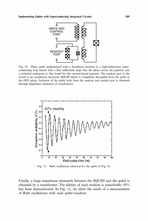
Implementing Qubits with Superconducting Integrated Circuits 189
WRITE ANDCONTROL
PORT
READOUTPORT
Fig. 10. Phase qubit implemented with a Josephson junction in a high-inductance super-conducting loop biased with a flux sufficiently large that the phase across the junction seesa potential analogous to that found for the current-biased junction. The readout part of thecircuit is an asymmetric hysteretic SQUID which is completely decoupled from the qubit inthe OFF phase. Isolation of the qubit both from the readout and control port is obtainedthrough impedance mismatch of transformers.
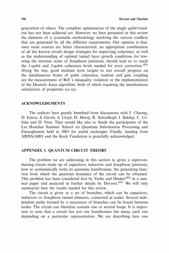
Fig. 11. Rabi oscillations observed for the qubit of Fig. 10.
Finally, a large impedance mismatch between the SQUID and the qubit isobtained by a transformer. The fidelity of such readout is remarkable: 95%has been demonstrated. In Fig. 11, we show the result of a measurementof Rabi oscillations with such qubit+readout.

190 Devoret and Martinis
WRITE ANDCONTROL PORT
READOUTPORT
Fig. 12. “Quantronium" circuit consisting of a Cooper-pair box with a non-linear induc-tive readout. A Wheatstone bridge configuration decouples qubit and readout variables whenreadout is OFF. Impedance mismatch isolation is also provided by additional capacitance inparallel with readout junction.
8.4. Cooper-pair Box with Non-linear Inductive Readout: The“Quantronium” Circuit
The Cooper-pair box needs to be operated at its “sweet spot” (degen-eracy point) where the transition frequency is to first order insensitive tooffset charge fluctuations. The “Quantronium” circuit presented in Fig. 12is a 3-junction bridge configuration with two small junctions defining aCooper box island, and thus a charge-like qubit which is coupled capac-itively to the write and control port (high-impedance port). There is alsoa large third junction, which provides a non-linear inductive coupling tothe read port. When the read port current I is zero, and the flux throughthe qubit loop is zero, noise coming from the read port is decoupledfrom the qubit, provided that the two small junctions are identical both incritical current and capacitance. When I is non-zero, the junction bridge isout of balance and the state of the qubit influences the effective non-linearinductance seen from the read port. A further protection of the impedancemismatch type is obtained by a shunt capacitor across the large junc-tion: at the resonance frequency of the non-linear resonator formed bythe large junction and the external capacitance C, the differential modeof the circuit involved in the readout presents an impedance of the orderof an ohm, a substantial decoupling from the 50 � transmission line car-rying information to the amplifier stage. The readout protocol involves aDC pulse(22,30) or an RF pulse(31) stimulation of the readout mode. Theresponse is bimodal, each mode corresponding to a state of the qubit.Although the theoretical fidelity of the DC readout can attain 95%, only amaximum of 40% has been obtained so far. The cause of this discrepancyis still under investigation.
In Fig. 13 we show the result of a Ramsey fringe experiment dem-onstrating that the coherence quality factor of the quantronium can reach

Implementing Qubits with Superconducting Integrated Circuits 191
Fig. 13. Measurement of Ramsey fringes for the Quantronium. Two π/2 pulses separatedby a variable delay are applied to the qubit before measurement. The frequency of the pulseis slightly detuned from the transition frequency to provide a stroboscopic measurement ofthe Larmor precession of the qubit.
25,000 at the sweet spot.(22) By studying the degradation of the qubitabsorption line and of the Ramsey fringes as one moves away from thesweet spot, it has been possible to show that the residual decoherence islimited by offset charge noise and by flux noise.(32) In principle, the influ-ence of these noises could be further reduced by a better optimizationof the qubit design and parameters. In particular, the operation of thebox can tolerate ratios of EJ/EC around 4 where the sensitivity to offsetcharge is exponentially reduced and where the non-linearity is still of order15%. The quantronium circuit has so far the best coherence quality factor.We believe this is due to the fact that critical current noise, one dominantintrinsic source of noise, affects this qubit far less than the others, rela-tively speaking, as can be deduced from the qubit hamiltonians of Sec. 6.
8.5. 3-Junction Flux Qubit with Built-in Readout
Figure 14 shows a third example of built-in readout, this time fora flux-like qubit. The qubit by itself involves three junctions in a loop,the larger two of the junctions playing the role of the loop inductancein the basic RF-SQUID.(33) The advantage of this configuration is toreduce the sensitivity of the qubit to external flux variations. The read-out part of the circuit involves two other junctions forming a hystereticDC-SQUID whose offset flux depends on the qubit flux state. The criti-cal current of this DC-SQUID has been probed by a DC pulse, but an

192 Devoret and Martinis
READOUTPORT
WRITE ANDCONTROL
PORT
Fig. 14. Three-junction flux qubit with a non-linear inductive readout. The medium-sizejunctions play the role of an inductor. Bridge configuration for nulling out back-action ofreadout is also employed here, as well as impedance mismatch provided by additional capac-itance.
Fig. 15. Ramsey fringes obtained for qubit of Fig. 14.
RF pulse could be applied as in another flux readout. Similarly to the twoprevious cases, the readout states 1c and 0c, which here correspond to theDC-SQUID having switched or not, map very well the qubit states |1〉 and|0〉, with a fidelity better than 60%. Here also, a bridge technique orthogo-nalizes the readout mode, which is the common mode of the DC-SQUID,and the qubit mode, which is coupled to the loop of the DC-SQUID.External capacitors provide additional protection through impedance mis-match. Figure 15 shows Ramsey oscillations obtained with this system.

Implementing Qubits with Superconducting Integrated Circuits 193
8.6. Too much On-chip Dissipation is Problematic: Do not Stir up the Dirt
All the circuits above include an on-chip amplification scheme pro-ducing high-level signals which can be read directly by high-temperaturelow-noise electronics. In the second and third examples, these signals leadto non-equilibrium quasi-particle excitations being produced in the nearvicinity of the qubit junctions. An elegant experiment has recently dem-onstrated that the presence of these excitations increases the offset chargenoise.(34) More generally, one can legitimately worry that large energydissipation on the chip itself will lead to an increase of the noises dis-cussed in Sec. 5.2. A broad class of new readout schemes addresses thisquestion.(31,35,36) They are based on a purely dispersive measurement ofa qubit susceptibility (capacitive or inductive). A probe signal is sentto the qubit. The signal is coupled to a qubit variable whose averagevalue is identical in the two qubit states (for instance, in the capacitivesusceptibility, the variable is the island charge in the charge qubit at thedegeneracy point). However, the susceptibility, which is the derivative ofthe qubit variable with respect to the probe, differs from one qubit stateto the other. The resulting state-dependent phase shift of the reflected sig-nal is thus amplified by a linear low temperature amplifier and finally dis-criminated at high temperature against an adequately chosen threshold.In addition to being very thrifty in terms of energy being dissipated onchip, these new schemes also provide a further natural decoupling action:when the probe signal is off, the back-action of the amplifier is also com-pletely shut off. Finally, the interrogation of the qubit in a frequency bandexcluding zero facilitates the design of very efficient filters.
9. COUPLING SUPERCONDUCTING QUBITS
A priori, three types of coupling scheme can be envisioned:
(a) In the first type, the transition frequency of the qubits are all equaland the coupling between any pair is switched on using one or sev-eral junctions as non-linear elements.(37,38)
(b) In the second type, the couplings are fixed, but the transition frequen-cies of a pair of qubits, originally detuned, are brought on resonancewhen the coupling between them needs to be turned on.(39–41)
(c) In the third type, which bears close resemblance to the methods usedin NMR,(1) the couplings and the resonance frequencies of the qubitsremain fixed, the qubits being always detuned. Being off-diagonal,the coupling elements have negligible action on the qubits. However,when a strong micro-wave field is applied to the target and control

194 Devoret and Martinis
qubits their resonant frequency with an appropriate amplitude, theybecome in “speaking terms” for the exchange of energy quanta andgate action can take place.(42)
So far only scheme (b) has been tested experimentally.The advantage of schemes (b) and (c) is that they work with purely
passive reactive elements like capacitors and inductors which shouldremain very stable as a function of time and which also should presentvery little high-frequency noise. In a way, we must design quantum inte-grated circuits in the manner that vacuum tube radios were designed inthe 1950s: only six tubes were used for a complete heterodyne radio set,including the power supply. Nowadays several hundreds of transistors areused in a radio or any hi-fi system. In that ancient era of classical elec-tronics, linear elements like capacitors, inductors or resistors were “free”because they were relatively reliable whereas tubes could break down eas-ily. We have to follow a similar path in quantum integrated circuit, the reli-ability issues having become noise minimization issues.
10. CAN COHERENCE BE IMPROVED WITH BETTERMATERIALS?
Up to now, we have discussed how, given the power spectral densi-ties of the noises �Qr, �EC and �EJ, we could design a qubit equippedwith control, readout and coupling circuits. It is worthwhile to ask at thispoint if we could improve the material properties to improve the coher-ence of the qubit, assuming all other problems like noise in the controlchannels and the back-action of the readout have been solved. A modelput forward by one of us (JMM) and collaborators shed some light onthe direction one would follow to answer this question. The 1/f spec-trum of the materials noises suggests that they all originate from 2-levelfluctuators in the amorphous alumina tunnel layer of the junction itself,or its close vicinity. The substrate or the surface of the superconductingfilms are also suspect in the case of �Qr and �EC but their influencewould be relatively weaker and we ignore them for simplicity. These two-level systems are supposed to be randomly distributed positional degreesof freedom ξi with effective spin-1/2 properties, for instance an impurityatom tunneling between two adjacent potential well. Each two-level sys-tem is in principle characterized by three parameters: the energy splitting�ωi , and the two coefficients αi and βi of the Pauli matrix representa-tion of ξi = αiσiz + βiσix (z is here by definition the eigen-energy axis).The random nature of the problem leads us to suppose that αi and βi
are both Gaussian random variables with the same standard deviation ρi .

Implementing Qubits with Superconducting Integrated Circuits 195
By carrying a charge, the thermal and quantum motion of ξi can contrib-
ute to �Qr = ∑i qiξi and �EC = ∑
i ciβ2
i
ωiσiz. Likewise, by modifying the
transmission of a tunneling channel in its vicinity, the motion of ξi cancontribute to �EJ = ∑
i giξi . We can further suppose that the quality ofthe material of the junction is simply characterized by a few numbers. Theessential one is the density ν of the transition frequencies ωi in frequencyspace and in real space, assuming a ω−1 distribution (this is necessary toexplain the 1/f behavior) and a uniform spatial distribution on the sur-face of the junction. Recent experiments indicate that the parameter ν isof order 105 µm−2 per decade. Then, assuming a value for ρi independentof frequency, only one coefficient is needed per noise, namely, the averagemodulation efficiency of each fluctuator. Such analysis provides a commonlanguage for describing various experiments probing the dependence of de-coherence on the material of the junction. Once the influence of the junc-tion fabrication parameters (oxydation pressure and temperature, impuritycontents, and so on) on these noise intensities will be known, it will bepossible to devise optimized fabrication procedures, in the same way per-haps as the 1/f noise in C-MOS transistors has been reduced by carefulmaterial studies.
11. CONCLUDING REMARKS AND PERSPECTIVES
The logical thread through this review of superconducting qubits hasbeen the question “What is the best qubit design?”. Because some crucialexperimental data is still missing, we unfortunately, at present, cannot con-clude by giving a definitive answer to this complex optimization problem.
Yet, a lot has already been achieved, and superconducting qubits arebecoming serious competitors of trapped ions and atoms. The followingproperties of quantum circuits have been demonstrated:
(a) Coherence quality factors Qϕ =Tϕω01 can attain at least 2×10⁴.(b) Readout and reset fidelity can be greater than 95%.(c) All states on the Bloch sphere can be addressed.(d) Spin echo techniques can null out low frequency drift of offset
charges.(e) Two qubits can be coupled and RF pulses can implement gate oper-
ation.(f) A qubit can be fabricated using only optical lithography techniques.
The major problem we are facing is that these various results have notbeen obtained at the same time IN THE SAME CIRCUIT, although suc-cesful design elements in one have often been incorporated into the next
196 Devoret and Martinis
generation of others. The complete optimization of the single qubit+read-out has not been achieved yet. However, we have presented in this reviewthe elements of a systematic methodology resolving the various conflictsthat are generated by all the different requirements. Our opinion is that,once noise sources are better characterized, an appropriate combinationof all the known circuit design strategies for improving coherence, as wellas the understanding of optimal tunnel layer growth conditions for low-ering the intrinsic noise of Josephson junctions, should lead us to reachthe 1-qubit and 2-qubit coherence levels needed for error correction.(45)
Along the way, good medium term targets to test overall progress onthe simultaneous fronts of qubit coherence, readout and gate couplingare the measurement of Bell ’s inequality violation or the implementationof the Deutsch–Josza algorithm, both of which requiring the simultaneoussatisfaction of properties (a)–(e).
ACKNOWLEDGMENTS
The authors have greatly benefited from discussions with I. Chuang,D. Esteve, S. Girvin, S. Lloyd, H. Mooij, R. Schoelkopf, I. Siddiqi, C. Ur-bina and D. Vion. They would like also to thank the participants of theLes Houches Summer School on Quantum Information Processing andEntanglement held in 2003 for useful exchanges. Finally, funding fromARDA/ARO and the Keck Fundation is gratefully acknowledged.
APPENDIX 1. QUANTUM CIRCUIT THEORY
The problem we are addressing in this section is, given a supercon-ducting circuit made up of capacitors, inductors and Josephson junctions,how to systematically write its quantum hamiltonian, the generating func-tion from which the quantum dynamics of the circuit can be obtained.This problem has been considered first by Yurke and Denker(46) in a sem-inal paper and analyzed in further details by Devoret.(47) We will onlysummarize here the results needed for this review.
The circuit is given as a set of branches, which can be capacitors,inductors or Josephson tunnel elements, connected at nodes. Several inde-pendent paths formed by a succession of branches can be found betweennodes. The circuit can therefore contain one or several loops. It is impor-tant to note that a circuit has not one hamiltonian but many, each onedepending on a particular representation. We are describing here one

Implementing Qubits with Superconducting Integrated Circuits 197
particular type of representation, which is usually well adapted to cir-cuits containing Josephson junctions. Like in classical circuit theory, aset of independent current and voltages has to be found for a particularrepresentation. We start by associating to each branch b of the circuit, thecurrent ib flowing through it and the voltage vb across it (a convention hasto be made first on the direction of the branches). Kirchhoff’s laws imposerelations among branch variables and some of them are redundant. Thefollowing procedure is used to eliminate redundant branches: one node ofthe circuit is first chosen as ground. Then from the ground, a loop-freeset of branches called spanning tree is selected. The rule behind the selec-tion of the spanning tree is the following: each node of the circuit must belinked to the ground by one and only one path belonging to the tree. Ingeneral, inductors (linear or non-linear) are preferred as branches of thetree but this is not necessary. Once the spanning tree is chosen (note thatwe still have many possibilities for this tree), we can associate to each nodea “node voltage” vn which is the algebraic sum of the voltages along thebranches between ground and the node. The conjugate “node current” inis the algebraic sum of all currents flowing to the node through capaci-tors ONLY. The dynamical variables appearing in the hamiltonian of thecircuit are the node fluxes and node charges defined as
φn =∫ t
−∞v (t1) dt1,
qn =∫ t
−∞i (t1) dt1.
Using Kirchhoff’s laws, it is possible to express the flux and thecharge of each branch as a linear combination of all the node fluxesand charges, respectively. In this inversion procedure, important physicalparameters appear: the magnetic fluxes through the loops imposed byexternal static magnetic fields and the polarization charges imposed bycharge bias sources.
If we now sum the energies of all branches of the circuit expressedin terms of node flux and charges, we will obtain the hamiltonian ofthe circuit corresponding to the representation associated with the par-ticular spanning tree. In this hamiltonian, capacitor energies behave likekinetic terms while the inductor energies behave as potential terms. Thehamiltonian of the LC circuit written in Sec. 2 is an elementary exampleof this procedure.
Once the hamiltonian is obtained it is easy get its quantum version byreplacing all the node fluxes and charges by their quantum operator equiv-alent. The flux and charge of a node have a commutator given by i�, like

198 Devoret and Martinis
the position and momentum of a particle
φ → φ,
q → q,[φ, q
]= i�.
One can also show that the flux and charge operators correspondingto a branch share the same commutation relation. Note that for the spe-cial case of the Josephson element, the phase θ and Cooper pair numberN , which are its dimensionless electric variables, have the property[
θ , N]= i.
In the so-called charge basis, we have
N =∑N
N |N〉 〈N | ,
cos θ = 12
∑N
(|N〉 〈N +1|+ |N+〉 〈N |)
while in the so-called phase basis, we have
N =|θ〉 ∂
i∂〈θ | .
Note that since the Cooper pair number N is an operator with integereigenvalues, its conjugate variable θ , has eigenvalues behaving like angles,i.e., they are defined only modulo 2π .
In this review, outside this appendix, we have dropped the hat onoperators for simplicity.
APPENDIX 2. EIGENENERGIES AND EIGENFUNCTIONSOF THE COOPER PAIR BOX
From Appendix 1, it easy to see that the hamiltonian of the Cooperpair box leads to the Schrodinger equation[
EC
(∂
i ∂θ−Ng
)2
−EJ cos θ
]�k(θ)=Ek�k(θ).

Implementing Qubits with Superconducting Integrated Circuits 199
The functions �k (θ) e−iNg and energies Ek are solutions of the Mat-hieu equation and can be found with arbitrary precision for all values ofthe parameters Ng and EJ/EC.(48) For instance, using the program Math-ematica, we find
Ek = ECMA
[k +1− (k +1)mod 2+2Ng(−1)k,−2EJ/EC
],
�k (θ) = eiNgθ
√2π
{MC
[4Ek
EC,−2EJ
EC,θ
2
]+ i(−1)k+1MS
[4Ek
EC,−2EJ
EC,θ
2
]},
where MA(r, q)=MathieuCharacteristicA[r,q],MC (a, q, z)=MathieuC[a,q,z],MS (a, q, z)=MathieuS[a,q,z].
APPENDIX 3. RELAXATION AND DECOHERENCE RATESFOR A QUBIT
Definition of the Rates
We start by introducing the spin eigenreference frame z, x and y con-sisting of the unit vector along the eigenaxis and the associated orthogonalunit vectors (x is in the XZ plane). For instance, for the Cooper pair box,we find that z = cos αZ + sin αX, with tan α = 2EC
(Ng −1/2
)/EJ, while
x =− sin αZ + cos αX.Starting with −→
S pointing along x at time t = 0, the dynamics of theBloch vector in absence of relaxation or decoherence is
−→S 0(t)= cos(ω01)x + sin(ω01)y
In presence of relaxation and decoherence, the Bloch vector will devi-ate from −→
S 0 (t) and will reach eventually the equilibrium value Seqz z,
where Seqz = tanh (�ω01/2kBT ).
We define the relaxation and decoherence rates as
�1 = limt→∞
ln⟨Sz(t)−S
eqz
⟩t
,
�φ = limt→∞
ln
[⟨−→S (t).
−→S 0(t)
⟩∣∣∣−→S (t)−S
eqz z
∣∣∣]
t.
Note that these rates have both a useful and rigorous meaning only ifthe evolution of the components of the average Bloch vector follows, after

200 Devoret and Martinis
a negligibly short settling time, an exponential decay. The �1 and �φ ratesare related to the NMR spin relaxation times T1 and T2
(49) by
T1 = �−11 ,
T2 = (�φ +�1/2
)−1.
The T2 time can be seen as the net decay time of quantum informa-tion, including the influence of both relaxation and dephasing processes.In our discussion of superconducting qubits, we must separate the contri-bution of the two type of processes since their physical origin is in generalvery different and cannot rely on the T2 time alone.
Expressions for the Rates
The relaxation process can be seen as resulting from unwanted tran-sitions between the two eigenstate of the qubit induced by fluctuations inthe effective fields along the x and y axes. Introducing the power spectraldensity of this field, one can demonstrate from Fermi’s Golden Rule that,for perturbative fluctuations,
�1 = Sx(ω01)+Sy(ω01)
�2
.
Taking the case of the Cooper-pair box as an example, we find thatSy(ω01)=0 and that
Sx(ω)=∫ +∞
−∞dt eiωt 〈A(t)A(0)〉+〈B(t)B(0)〉 ,
where
A(t) = �EJ(t)Eel
2√
E2J +E2
el
,
B(t) = EJ�Eel(t)
2√
E2J +E2
el
,
Eel = 2EC(Ng −1/2).
Since the fluctuations �Eel(t) can be related to the impedance of theenvironment of the box,(19,21,50) an order of magnitude estimate of therelaxation rate can be performed, and is in rough agreement with obser-vations.(22,51)

Implementing Qubits with Superconducting Integrated Circuits 201
The decoherence process, on the other hand, is induced by fluctua-tions in the effective field along the eigenaxis z. If these fluctuations areGaussian, with a white noise spectral density up to frequencies of orderseveral �φ (which is often not the case because of the presence of 1/fnoise) we have
�φ = Sz (ω�0)
�2
.
In presence of a low frequency noise with an 1/f behavior, the formulais more complicated.(52) If the environment producing the low frequencynoise consists of many degrees of freedom, each of which is very weaklycoupled to the qubit, then one is in presence of classical dephasing which,if slow enough, can in principle be fought using echo techniques. If, onethe other hand, only a few degrees of freedom like magnetic spins orglassy two-level systems are dominating the low frequency dynamics, deph-asing is quantum and not correctable, unless the transition frequencies ofthese few perturbing degrees of freedom is itself very stable.
REFERENCES
1. M. A. Nielsen and I. L. Chuang, Quantum Computation and Quantum Information (Cam-bridge, 2000).
2. M. Tinkham, Introduction to Superconductivity (Krieger, Malabar, 1985).3. J. M. Martinis, M. H. Devoret, J. Clarke, Phys. Rev. Lett. 55, 1543 (1985); M. H. Dev-
oret, J. M. Martinis, J. Clarke, Phys. Rev. Lett. 55, 1908 (1985); J. M. Martinis, M. H.Devoret and J. Clarke, Phys. Rev. 35, 4682 (1987).
4. J. M. Martinis and M. Nahum, Phys Rev. B 48, 18316 (1993).5. B. D. Josephson, in Superconductivity, R. D. Parks (ed.) (Marcel Dekker, New York,
1969).6. K. K. Likharev, Dynamics of Josephson Junctions and Circuits (Gordon and Breach, New
York, 1986).7. I. Giaever, Phys. Rev. Lett. 5, 147, 464 (1960).8. A. O. Caldeira and A. J. Leggett, Ann. Phys. (N.Y.) 149, 347 (1983); A. J. Leggett,
J. Phys. CM 14, R415 (2002).9. D. P. DiVincenzo, arXiv:quant-ph/0002077.
10. R. P. Feynman, Lectures on Physics, Vol. 2, Chap. 23, (Addison-Wesley, Reading, 1964).11. D. C. Mattis and J. Bardeen, Phys. Rev. 111, 412 (1958).12. P. G. de Gennes, Superconductivity of Metals and Alloys (Benjamin, New York, 1966).13. J. M. Raimond, M. Brune, and S. Haroche, Rev. Mod. Phys. 73, 565 (2001).14. J. M. Martinis and K. Osborne, in Quantum Information and Entanglement, eds. J. M.
Raimond, D. Esteve, and J. Dalibard, Les Houches Summer School Series, arXiv:cond-mat/0402430.
15. J. Clarke, Proc. IEEE 77, 1208 (1989).16. D. J. Van Harlingen, B. L. T. Plourde, T. L. Robertson, P. A. Reichardt, and John
Clarke, preprint.

202 Devoret and Martinis
17. R. W. Simmonds, K. M. Lang, D. A. Hite, D. P. Pappas, and J. M. Martinis, acceptedfor publication in Phys. Rev. Lett.
18. M. Buttiker, Phys. Rev. B 36, 3548 (1987).19. V. Bouchiat, D. Vion, P. Joyez, D. Esteve, M. H. Devoret, Physica Scripta T 76, 165
(1998).20. Y. Nakamura , Yu. A. Pashkin, and J. S. Tsai, Nature 398, 786 (1999).21. Yu. Makhlin, G. Schon, and A. Shnirman, Rev. Mod. Phys. 73, 357 (2001).22. D. Vion, A. Aassime, A. Cottet, P. Joyez, H. Pothier, C. Urbina, D. Esteve, and M. H.
Devoret, Science 296, 286 (2002).23. A. Barone and G. Paterno, Physics and Applications of the Josephson Effect (Wiley, New
York, 1992).24. S. Han, R. Rouse, and J. E. Lukens, Phys. Rev. Lett. 84, 1300 (2000); J. R. Friedman,
V. Patel, W. Chen, S. K. Tolpygo, and J. E. Lukens, Nature 406, 43 (2000).25. J. E. Mooij, T. P. Orlando, L. Levitov, Lin Tian, C. H. van der Wal, and S. Lloyd,
Science 285, 1036 (1999); C. H. van der Wal, A. C. J. ter Haar, F. K. Wilhem, R. N.Schouten, C. Harmans, T. P. Orlando, S. Loyd, and J. E. Mooij, Science 290, 773 (2000).
26. J. M. Martinis, S. Nam, J. Aumentado, and C. Urbina, Phys. Rev. Lett. 89, 117901(2002).
27. M. Steffen, J. Martinis, and I. L. Chuang, PRB 68, 224518 (2003).28. M. H. Devoret and R. J. Schoelkopf, Nature 406, 1039 (2002).29. A. N. Korotkov and D. V. Averin, Phys. Rev. B 64, 165310 (2001).30. A. Cottet, D. Vion, A. Aassime, P. Joyez, D. Esteve, and M. H. Devoret, Physica C 367,
197 (2002).31. I. Siddiqi, R. Vijay, F. Pierre, C. M. Wilson, M. Metcalfe, C. Rigetti, L. Frunzio, and
M. H. Devoret, cond-mat/0312623, submitted to Phys. Rev. Lett.32. D. Vion, A. Aassime, A. Cottet, P. Joyez, H. Pothier, C. Urbina, D. Esteve, and M. H.
Devoret, Fortschritte der Physik 51, 462 (2003).33. I. Chiorescu, Y. Nakamura, C. J. P. M. Harmans, and J. E. Mooij, Science 299, 1869
(2003).34. J. Mannik and J. E. Lukens, Phys. Rev. Lett. 92, 057004 (2004).35. A. Wallraff, D. I. Schuster, A. Blais, L. Frunzio, R.-S. Huang, J. Majer, S. Kumar, S. M.
Girvin, R. J. Schoelkopf, cond-mat/0408367, accepted by Nature.36. A. Lupascu, C. J. M. Verwijs, R. N. Schouten, C. J. P. M. Harmans, J. E. Mooij, cond-
mat/0311510, submitted to Phys. Rev. Lett.37. Variable electrostatic transformer: controllable coupling of two charge qubits, D.V. Aver-
in, C. Bruder, Phys. Rev. Lett. 91, 057003 (2003).38. A. Blais, A. Maassen van den Brink, A. M. Zagoskin, Phys. Rev. Lett. 90, 127901 (2003)39. A. Pashkin Yu, T. Yamamoto, O. Astafiev, Y. Nakamura, D. V. Averin, and J. S. Tsai,
Nature 421 (2003).40. J. B. Majer, Superconducting Quantum Circuits, PhD Thesis, TU Delft, (2002);
J. B. Majer, F. G. Paauw, A. C. J. ter Haar, C. P. J. Harmans, and J. E. Mooij,arXiv:cond-mat/0308192.
41. A. J. Berkley, H. Xu, R. C. Ramos, M. A. Gubrud, F. W. Strauch, P. R. Johnson, J. R.Anderson, A. J. Dragt, C. J. Lobb, and F. C. Wellstood, Science 300, 1548 (2003).
42. C. Rigetti and M. Devoret, unpublished.43. Y. Nakamura, A. Pashkin Yu, and J. S. Tsai, Phys. Rev. Lett. 88, 047901 (2002).44. D. Vion, A. Aassime, A. Cottet, P. Joyez, H. Pothier, C. Urbina, D. Esteve, and M. H.
Devoret, Forts. der Physik 51, 462 (2003); E. Collin, G. Ithier, A. Aassime, P. Joyez, D.Vion and D. Esteve, submitted.
45. J. Preskill, J. Proc. R. Soc. London Ser. A 454, 385 (1998).

Implementing Qubits with Superconducting Integrated Circuits 203
46. B. Yurke and J. S. Denker, Phys. Rev. A 29, 1419 (1984).47. M. H. Devoret in “Quantum Fluctuations” , S. Reynaud, E. Giacobino, J. Zinn-Justin
(eds.) (Elsevier, Amsterdam, 1996), p. 351.48. A. Cottet, Implementation of a quantum bit in a superconducting circuit, PhD Thesis, Uni-
versite Paris 6, 2002.49. A. Abragam, Principles of Nuclear Magnetic Resonance (Oxford University Press,
Oxford, 1985).50. R. J. Schoelkopf, A. A. Clerk, S. M. Girvin, K. W. Lehnert, and M. H. Devoret. ar-
Xiv:cond-mat/0210247.51. K. W. Lehnert, K. Bladh, L. F. Spietz, D. Gunnarsson, D. I. Schuster, P. Delsing, and
R. J. Schoelkopf, Phys. Rev.Lett. 90, 027002 (2002).52. J. M. Martinis, S. Nam, J. Aumentado, K. M. Lang, and C. Urbina, Phys. Rev. B 67, 462
(2003).