imaging and manipulating electrons in a 1d quantum dot
TRANSCRIPT
Imaging and Manipulating Electrons in a 1D Quantum Dot with Coulomb Blockade Microscopy
CitationQian, Jiang, Bertrand Halperin, and Eric Heller. 2010. Imaging and manipulating electrons in a 1D quantum dot with Coulomb blockade microscopy. Physical Review B 81(12): 125323.
Published Versiondoi:10.1103/PhysRevB.81.125323
Permanent linkhttp://nrs.harvard.edu/urn-3:HUL.InstRepos:7486326
Terms of UseThis article was downloaded from Harvard University’s DASH repository, and is made available under the terms and conditions applicable to Open Access Policy Articles, as set forth at http://nrs.harvard.edu/urn-3:HUL.InstRepos:dash.current.terms-of-use#OAP
Share Your StoryThe Harvard community has made this article openly available.Please share how this access benefits you. Submit a story .
Accessibility

arX
iv:0
809.
0834
v2 [
cond
-mat
.mes
-hal
l] 1
9 M
ar 2
010
Imaging and manipulating electrons in a 1D quantum dot with Coulomb blockade microscopy
Jiang Qian1,2, Bertrand I. Halperin1 and Eric J. Heller11 Physics Department, Harvard University, Cambridge, MA 02138, USA
2 Arnold Sommerfeld Center for Theoretical Physics and Center for NanoScience, Ludwig-Maximilians-Universitat Munchen, Germany(Dated: March 23, 2010)
Motivated by recent experiments by the Westervelt group, which used a mobile tip to probe the electronicstate of a segmented nanowire, we calculate shifts in Coulomb blockade peak positions, as a function of tiplocation, which we term “Coulomb blockade microscopy”. We show that if the tip can be brought sufficientlyclose to the nanowire, one can distinguish a high density electronic liquid state from a Wigner crystal state bymicroscopy with a weak tip potential. In the opposite limit of a strongly negative tip potential, the potentialdepletes the electronic density under it and divides the quantum wire into two partitions. There the tip can pushindividual electrons from one partition to the other, and the Coulomb blockade micrograph can clearly track suchtransitions. We show that this phenomenon can be used to qualitatively estimate the relative importance of theelectron interaction compared to one particle potential and kinetic energies. Finally, we propose that a weak tipCoulomb blockade micrograph focusing on the transition between electron numberN = 0 andN = 1 states maybe used to experimentally map the one-particle potential landscape produced by impurities and inhomogeneities.
I. INTRODUCTION
Studies of nanoscale electronic structures hold importantpromise both as laboratories for few-body, interacting quan-tum mechanical systems and as technological testbeds forfuture classical or quantum computing technologies. Novelprobe technologies1,2 are very important for studying elec-tronic properties in nanoscale systems because they are oftenbeyond the resolution of conventional imaging techniques likeoptical microscopy, and traditional transport measurementscan only measure spatially averaged physical properties suchas the conductance or the current. One scanning probe mi-croscopy (SPM)2 technique utilizes a charged metallic tip toperturb the local electronic density in a nanoelectronic struc-ture while monitoring the resulting change in transport prop-erties. Using this technique one can obtain spatially resolvedmeasurement of the electronic properties, including the localelectron density and, in principle, the wavefunction itself inthe case of a one-electron system3(see discussions below).This imaging technique has been fruitfully applied to studythe flow of ballistic electrons across a range of two dimen-sional heterostructures.
Recently, a series of experiments4 applied SPM techniquesto study quantum wires. In these experiments a segment ofan InAs nanowire lying on top of a two-dimensional SiOxlayer was isolated from the rest of the wire by two shortInP segments, forming a one-dimensional quantum dot withlithographically defined boundaries. A negatively chargedprobe scanned controllably the two dimensional area aroundthe wire and the conductance across the 1D quantum dot wasmeasured as a function of the probe location. Both the voltageof the probe and its height above the surface can also be inde-pendently varied. Motivated by these new experimental pos-sibilities, we turn to exact diagonalization techniques tostudythe conductance response of a few-electron quantum dot as afunction of a spatially varied probe potential, in order to illus-trate the kind of information that can be extracted in the caseof a system of several electrons.
FIG. 1: Schematic geometry of Coulomb blockade microscopy ofa quantum wire containing four electrons. When calculatingtheelectron-electron interaction and the electron-tip interaction, we as-sume that the InP barriers have zero thickness, the InAs wireis in-finitely long, and the substrate layers extend to infinity in xand ydirections.
II. MODEL
We consider a uniform InAs (dielectric constantε = 15.4,Bohr radiusaB ≈ 34nm) nanowire of radiusR= 10nm, whichlies in vacuum atop a SiOx (ε = 3.9) layer 100nm thick, sep-arating it from conducting doped bulk silicon (see Fig. 1).Electrons are modelled as point charges traveling along thecenter axis of the wire, confined to interval− L
2 < x < L2
by hard walls, representing the InP layers. We considerlength L from 110nm to 500nm. The electron-electron in-teractionU(x1 − x2) was calculated using the commercialfinite-element program ComsolTMto solve the classical Pois-son equation for a point charge on the axis of an infinite wireabove in a substrate with the geometry described in Fig. 1. Atshort distance∆x, the potential was softened to account forthe finite thickness of the electron wavefunction, by replac-ing ∆x−1 with [(∆x)2+R2]−1/2. Following the approximationused by Topinka5, we model the negatively charged probe as afixed point charge of strengthq at a location~r0 relative to thecenter point of the wire. This gives rise to a one-body poten-tial V(x;~r0,q) for an electron on the wire axis at pointx, whichwe again obtain by solving the Poisson equation (results are
2
0
10
20
30
40
50
60
0 100 200 300 400 500
0
4
8
12
16
20
-200 -100 0 100 200
U(
∆x) (meV)
V(x) (meV)
∆x (nm)
x (nm)
U(∆x)
V(x) z0= 30nm
z0= 50nm
z0=100nm
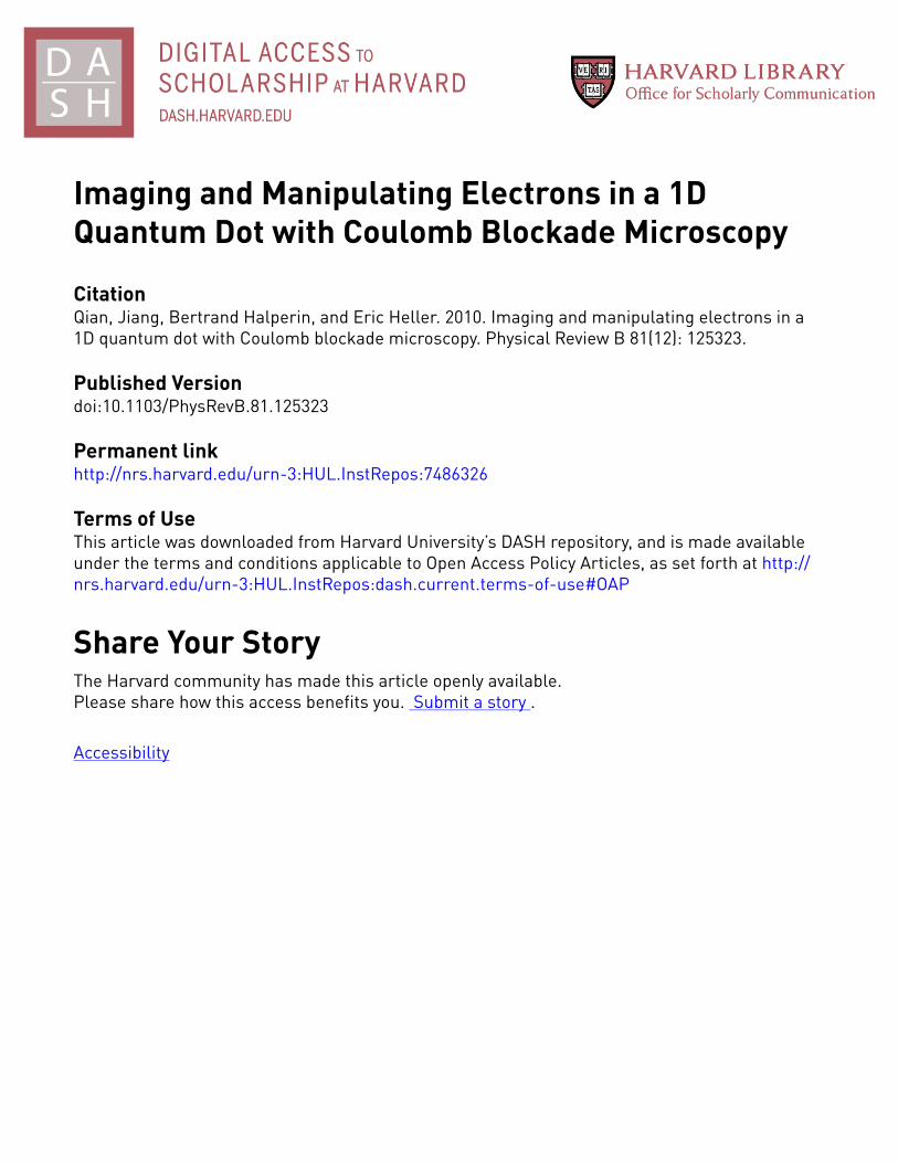
FIG. 2: (Color Online) (Dotted)Interaction potentialU(∆z).(Solid,long and short dashed) TipV(x) potentials with a tip chargeq = eand locations~r0 = (0,0,z0) wherez0 = 30nm,50nm,100nm.
shown in Fig. 2).In this paper, we diagonalize the exact 1D many-body
Hamiltonian with the Lanczos method6 for up to electronnumberN = 4:
−h2
2m∗∇2Ψ+
N
∑i=1
V(xi ;~r0,q)Ψ+N
∑i=1
i−1
∑j=1
U(xi ,x j)Ψ = E Ψ,
(1)where Ψ is the full many-body wavefunction, dependingon the positionxi and spinσi of the electrons. To con-nect to the experimentally observable variables, we considerthe Coulomb blockade peakpositionsof the transition from(N−1) to N electron ground states. The conductance throughthe quantum wire is maximum when the chemical potentialdifference between the lead and the wire, controlled by thevoltageVg on a back gate, is equal to the ground state en-ergy difference between the two states in question. We maywrite this condition as∆E ≡ EN −EN−1 = αVg + β , whereβ is a constant andα is the proportionality constant betweenchanges in the back gate voltage and the chemical potential inthe quantum dot. We probe the electronic states in the quan-tum wire through the dependence of∆E on the tip position~r0 and potential strengthq. An interesting set of spatially re-solved information about the electrons in the wire can be ex-tracted from this function, and we call this method “Coulombblockade microscopy”. It is a special application of the “scan-ning probe microscopy” developed by the Westervelt group2.In calculations in this paper we focus on the transition fromN = 3 to N = 4 electrons, but most of our conclusions areeasily generalizable to other ground state transitions.
Finally, we note that for four non-interacting electrons withspin in a wire of radiusR = 10nm, when the dot lengthL>Lm= 18.2nm, the lowest four single particle energy levelsare all longitudinal modes. The shortest wire length we con-sider in this paperL = 110nm≫ Lm, we therefore expect thewires under consideration can be well approximated as strictly1D under the assumption of weak interaction effects. Indeed,the gap between the transverse ground state and first excited
0
2
4
6
8
10
12
0 0.1 0.2 0.3 0.4 0.5
ρ(x)*L
x/L
L=110nm
L=500nm
FIG. 3: (Color Online) Electronic densities for aL= 110nmwire andfor a L = 500nmwire in absence of tip potential. Only the right halfis shown, as the plot is symmetric aboutx= 0. We rescale thex andρ(x) with wire lengthL to ease the comparison.
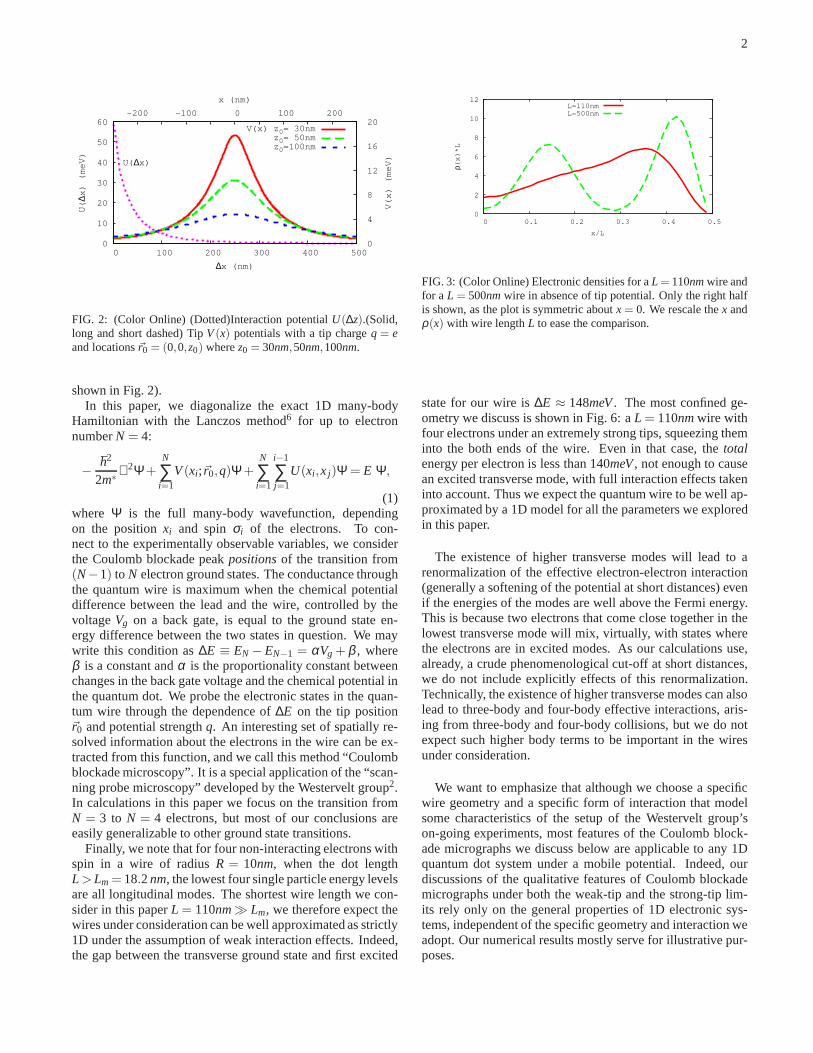
state for our wire is∆E ≈ 148meV. The most confined ge-ometry we discuss is shown in Fig. 6: aL = 110nmwire withfour electrons under an extremely strong tips, squeezing theminto the both ends of the wire. Even in that case, thetotalenergy per electron is less than 140meV, not enough to causean excited transverse mode, with full interaction effects takeninto account. Thus we expect the quantum wire to be well ap-proximated by a 1D model for all the parameters we exploredin this paper.
The existence of higher transverse modes will lead to arenormalization of the effective electron-electron interaction(generally a softening of the potential at short distances)evenif the energies of the modes are well above the Fermi energy.This is because two electrons that come close together in thelowest transverse mode will mix, virtually, with states wherethe electrons are in excited modes. As our calculations use,already, a crude phenomenological cut-off at short distances,we do not include explicitly effects of this renormalization.Technically, the existence of higher transverse modes can alsolead to three-body and four-body effective interactions, aris-ing from three-body and four-body collisions, but we do notexpect such higher body terms to be important in the wiresunder consideration.
We want to emphasize that although we choose a specificwire geometry and a specific form of interaction that modelsome characteristics of the setup of the Westervelt group’son-going experiments, most features of the Coulomb block-ade micrographs we discuss below are applicable to any 1Dquantum dot system under a mobile potential. Indeed, ourdiscussions of the qualitative features of Coulomb blockademicrographs under both the weak-tip and the strong-tip lim-its rely only on the general properties of 1D electronic sys-tems, independent of the specific geometry and interaction weadopt. Our numerical results mostly serve for illustrativepur-poses.

3
9.48
9.52
9.56
9.6
9.64
9.68
0 50 100 150 200 250
E4-E3(meV)
x0 (nm)
z0= 30nm
z0= 50nm
z0=100nm
FIG. 4: (Color Online) Coulomb blockade micrographs for a 1Ddot with L = 500nm and tip chargeq = 0.02e for three tip poten-tial shown in Fig.2. Again, the right half is shown.
III. ELECTRONIC DENSITY
In the absence of a probe potentialV, both theN = 3 andN = 4 wires the electronic density profileρ(x) undergoes acrossover as a function ofL from a liquid state characterizedby a 2kF Friedel oscillations to a quasi-Wigner crystal statecharacterized by a 4kF density oscillation. Such a crossoverfrom a liquid state to quasi-Wigner states with a decrease indensity a very generic phenomenon for 1D interacting fermionsystem7,8. Indeed, for any interacting decaying no faster thanx−2 at long distance a quasi-Wigner crystal state is knownto emerge at low density8. This requirement for interactionwill hold for a system with long screening length as comparedto mean inter-particle distance, as is the case for our geom-etry when the screening doped silicon layer is relatively far(100µm) away. For our specific geometry and interaction, thecrossover happens at around densityρ∗ ≈ 35µm−1. A Wignercrystallized density variation is shown in the dashed curveofFig. 3 for a quantum dot ofL = 500nm, whereas forL = 110the four electron density exhibits Friedel oscillations.
IV. WEAK TIP LIMIT
Now we introduce a weak tip potential, corresponding to anegatively charged tip of strengthq= 0.02e, scanning abovethe center axis of the quantum wire along its direction(1,0,0),with the tip location vector~r0 = (x0,0,z0). For a 1D quan-tum dot of lengthL = 500nm, which as shown in Fig. 3 has4kF Wigner-crystal density variation, let us consider the threetip heights above the quantum wire,z0 = 30nm,50nm,100nm,corresponding to the three tip potential shown in Fig. 2. Theresulting Coulomb blockade peak position∆E as a function ofthe tip coordinatex0 along the wire, i.e. the Coulomb block-ade micrograph, is shown in Fig. 4. Clearly, in Fig. 2 thecloser the tip approaches the wire, the more localized is thetippotential and a sharper tip potential make it easier to resolvethe density variations, this is reflected in Coulomb blockademicrograph scans in Fig. 4. Atz0 = 30nm,50nmfrom the tipto the center of the wire, the 4kF density oscillation of the
73.62
73.64
73.66
73.68
0 10 20 30 40 50
9.48
9.52
9.56
9.6
9.64
9.68
0 50 100 150 200 250 300
L=110nm E4-E3(meV)
L=500nm E4-E3(meV)
L=110nm x0(nm)
L=500nm x0(nm)
L=110nm
L=500nm
FIG. 5: (Color Online)q = 0.02e weak tip limit for theN = 3 toN = 4 Coulomb blockade transition for densities shown in Fig. 3.The tip distance to the wire isz0 = 30nm. Only the right half isshown.
150
160
170
180
190
0 10 20 30 40 50 15
20
25
30
35
40 0 50 100 150 200 250 300
L=11
0nm
E4-
E3(
meV
)
L=50
0nm
E4-
E3(
meV
)
L=110nm x0(µm)
L=500nm x0(µm)
L=110nmL=500nm
FIG. 6: (Color Online)q= 8e strong tip limit for theN = 3 toN = 4Coulomb blockade transition for densities shown in Fig. 3 The tip towire distance is 30nm. Only the right half is scanned.
quasi-Wigner crystal state on the right can be detected in theCoulomb blockade micrograph, whereas whenz0 = 100nmaway, the tip potential becomes much too broad to resolve thefine features of the density oscillations. We note that althoughthe resolution of the tip is largely determined by the distancez0, the contrast of a Coulomb blockade micrograph, i.e. themagnitude of the 4kF variations in the micrographs, can beimproved by modestly increasing the tip potential.
By contrast, in Fig. 5 theL = 110nm micrograph atz0 =30nm does not show features of Wigner crystal oscillations.However, this micrograph does not by itself give a clearcutindication of the absence of Wigner crystal order forL =110nm. With the current interaction and tip parameters, onecannot observe the crossover from the Wigner crystal to theFriedel oscillations because it happens at a inter-particle spac-ing ∆x ≈ 30nm, below the resolution of the micrograph evenat z= 30nm. To be more specific, we may define the onsetof Wigner-crystal order for our four-electron system as thelengthL at which there first appears a local minimum of themean densityρ(x) in the vicinity of x/L = 0.25. Accordingto our calculations, this should occur at L=135 nm. However,with the tip at height 30nm, in the weak charge limit, the reso-
4
density
-250 -200 -150 -100 -50 0 50 100 150 200 250
x (nm)
0
100
200
300x 0
(nm
)
0
0.02
0.04
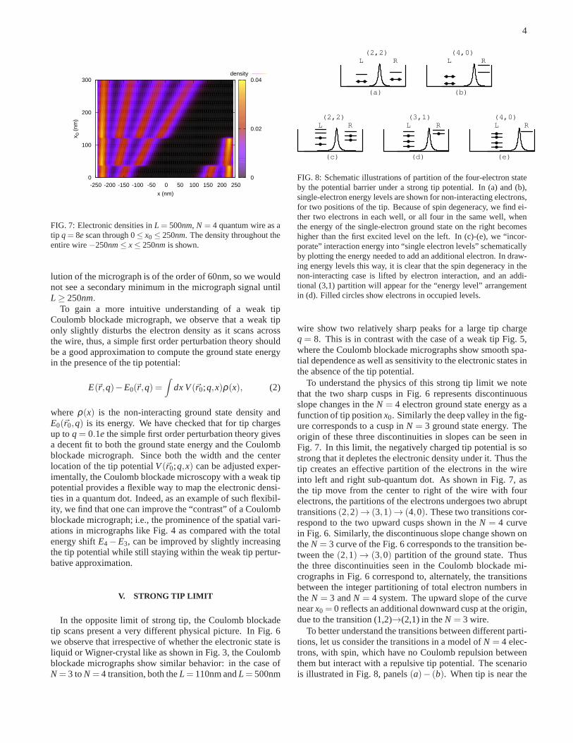
FIG. 7: Electronic densities inL = 500nm, N = 4 quantum wire as atip q= 8escan through 0≤ x0 ≤ 250nm. The density throughout theentire wire−250nm≤ x≤ 250nm is shown.
lution of the micrograph is of the order of 60nm, so we wouldnot see a secondary minimum in the micrograph signal untilL ≥ 250nm.
To gain a more intuitive understanding of a weak tipCoulomb blockade micrograph, we observe that a weak tiponly slightly disturbs the electron density as it scans acrossthe wire, thus, a simple first order perturbation theory shouldbe a good approximation to compute the ground state energyin the presence of the tip potential:
E(~r,q)−E0(~r ,q) =∫
dx V(~r0;q,x)ρ(x), (2)
whereρ(x) is the non-interacting ground state density andE0(~r0,q) is its energy. We have checked that for tip chargesup toq= 0.1e the simple first order perturbation theory givesa decent fit to both the ground state energy and the Coulombblockade micrograph. Since both the width and the centerlocation of the tip potentialV(~r0;q,x) can be adjusted exper-imentally, the Coulomb blockade microscopy with a weak tippotential provides a flexible way to map the electronic densi-ties in a quantum dot. Indeed, as an example of such flexibil-ity, we find that one can improve the “contrast” of a Coulombblockade micrograph; i.e., the prominence of the spatial vari-ations in micrographs like Fig. 4 as compared with the totalenergy shiftE4−E3, can be improved by slightly increasingthe tip potential while still staying within the weak tip pertur-bative approximation.
V. STRONG TIP LIMIT
In the opposite limit of strong tip, the Coulomb blockadetip scans present a very different physical picture. In Fig.6we observe that irrespective of whether the electronic state isliquid or Wigner-crystal like as shown in Fig. 3, the Coulombblockade micrographs show similar behavior: in the case ofN= 3 toN= 4 transition, both theL= 110nm andL= 500nm
(2,2)
(a)
RL
(4,0)
(b)
RL
(2,2)
(c)
RL
(3,1)
(d)
RL
(4,0)
(e)
RL
FIG. 8: Schematic illustrations of partition of the four-electron stateby the potential barrier under a strong tip potential. In (a)and (b),single-electron energy levels are shown for non-interacting electrons,for two positions of the tip. Because of spin degeneracy, we find ei-ther two electrons in each well, or all four in the same well, whenthe energy of the single-electron ground state on the right becomeshigher than the first excited level on the left. In (c)-(e), we“incor-porate” interaction energy into “single electron levels” schematicallyby plotting the energy needed to add an additional electron.In draw-ing energy levels this way, it is clear that the spin degeneracy in thenon-interacting case is lifted by electron interaction, and an addi-tional (3,1) partition will appear for the “energy level” arrangementin (d). Filled circles show electrons in occupied levels.
wire show two relatively sharp peaks for a large tip chargeq= 8. This is in contrast with the case of a weak tip Fig. 5,where the Coulomb blockade micrographs show smooth spa-tial dependence as well as sensitivity to the electronic states inthe absence of the tip potential.
To understand the physics of this strong tip limit we notethat the two sharp cusps in Fig. 6 represents discontinuousslope changes in theN = 4 electron ground state energy as afunction of tip positionx0. Similarly the deep valley in the fig-ure corresponds to a cusp inN = 3 ground state energy. Theorigin of these three discontinuities in slopes can be seen inFig. 7. In this limit, the negatively charged tip potential is sostrong that it depletes the electronic density under it. Thus thetip creates an effective partition of the electrons in the wireinto left and right sub-quantum dot. As shown in Fig. 7, asthe tip move from the center to right of the wire with fourelectrons, the partitions of the electrons undergoes two abrupttransitions(2,2)→ (3,1)→ (4,0). These two transitions cor-respond to the two upward cusps shown in theN = 4 curvein Fig. 6. Similarly, the discontinuous slope change shown ontheN = 3 curve of the Fig. 6 corresponds to the transition be-tween the(2,1) → (3,0) partition of the ground state. Thusthe three discontinuities seen in the Coulomb blockade mi-crographs in Fig. 6 correspond to, alternately, the transitionsbetween the integer partitioning of total electron numbersintheN = 3 andN = 4 system. The upward slope of the curvenearx0 = 0 reflects an additional downward cusp at the origin,due to the transition (1,2)→(2,1) in theN = 3 wire.
To better understand the transitions between different parti-tions, let us consider the transitions in a model ofN = 4 elec-trons, with spin, which have no Coulomb repulsion betweenthem but interact with a repulsive tip potential. The scenariois illustrated in Fig. 8, panels(a)− (b). When tip is near the

5
50
51
52
53
54
55
56
57
58
0.09 0.1 0.11 0.12 0.13 0.14 0.15 0.16 0.17 0.18 60
61
62
63
64
65
66
67
68
q=0.
6 E
4-E
3(m
eV)
q=1.
8 E
4-E
3(m
eV)
x0 (nm)
tip q=0.6tip q=1.8
FIG. 9: (Color Online).q= 0.6e andq= 1.8e intermediate tip po-tentials forN = 3 toN = 4 Coulomb blockade transition in a wire oflengthL = 180nm. The tip distance to the wire isz0 = 30nm. Onlythe right half is shown.
center of the wire, the electrons are partitioned(2,2) and bothelectrons in each side reside in the single-particle groundstate.As the tip moves rightward, the energy levels rise in the rightpartition and fall in the left. When the first excited level ontheleft partition crosses the ground state on the right,bothelec-trons will move to the left partition. Therefore, contrary to theinteracting case, there is no energetically favorable state of(3,1) partitioning in the non-interacting system. In theN = 3case, the(2,1) partition is not affected by this, and for non-interacting system the transition(2,1)→ (3,0) will coincidewith the transition inN = 4, so the Coulomb blockade micro-graph will show only a single peak. This analysis can alsobe generalized to a wire containing multiple non-interactingelectrons, such that all the(odd,odd) partitionings of elec-tron number will be missing.
As schematically illustrated in Fig. 8, panels(c)− (e),when we take electron interaction into consideration, the oneand two electron state would no longer be degenerate in eitherpartition, so contrary to the non-interacting scenarios inpanel(a)− (b), here a(3,1) partition can survive as an interme-diate stage between the(2,2) and(4,0) partitions. With thenon-interacting case in mind, we postulate that the distancebetween two peaks inN = 3 to N = 4 micrographs, corre-sponding to the tip positions where(3,1) partitioning in theN = 4 wire is stable, can serve as an indicator of the rela-tive importance of the interaction energy versus the sum ofkinetic and single particle potential energies. The less impor-tant interaction is compared to single particle energies, the lesssplitting would the one and two particle energies be, and thesmaller is the region of stable(3,1) partition. This can be seenin Fig. 6. The potential energy should have a larger share inthe total energy in the longer wire with lower electronic den-sity, and indeed we observe that the longer wire has a widerdistance between the two peaks marking(2,2) → (3,1) and(3,1)→ (4,0) transitions.
0
1
2
3
4
5
6
7
8
9
10
0 0.1 0.2 0.3 0.4 0.5
ρ(x)
*L
x/L
effective charge q=0 effective charge q=0.6effective charge q=1.8
FIG. 10: (Color Online) Electronic density for aL = 180nm wireunder three tip potentials, with effective chargesq = 0e, q = 0.6eandq= 1.8e. Only the right half is shown, as the plot is symmetricaboutx= 0. We rescale thex andρ(x) with the wire lengthL.
VI. INTERMEDIATE TIP CHARGE
We have carried out calculations with various tip chargesintermediate between the two limits discussed above. In gen-eral, the larger the charge on the tip, the more readily onesees the secondary minima in the micrograph signal, whichare seen in Fig. 6 for a chargeq = 8e, even atL = 110nm.As one illustration, for a wire of length 180 nm, with a tipheight of 30 nm, we find that the micrograph signal shows asecondary minimum atx/L ≈ 0.15 forq= 1.8e, but shows nosecondary minimum whenq = 0.6e, as seen in Fig. 9 How-ever, if we calculate the electron density in the wire whenthe tip is over the center of the wire (x0 = 0), we find thata tip charge ofq= 0.6e is enough to substantially modify thedensity relative to the density in the absence of the tip. Asseen in Fig. 10, the electron density below the tip, atx = 0is reduced by a factor of three relative to the density with notip charge. Nevertheless, the oscillations seen inρ(x) remainqualitatively similar to structure seen in the absence of the tip.For example, the charged tip only pushes out the position ofthe secondary minimum in the density fromx/L = 0.25 tox/L = 0.3.
In general, when we increase the tip potential to intermedi-ate values, the resolution of our micrographs improves com-pared with the weak tip limit. This is evident in the fact thatatq= 1.8ewe can already see signs of Wigner crystallization atL = 180nm, in contrast with the weak tip case withq= 0.02ewhere we can only detect quasi-Wigner crystal atL = 250nm.On the other hand, atq= 1.8e there isnosignature of Wignercrystallization when the electrons are in a liquid state in aL = 110nm wire. Thus we do not have ”false positive” sig-nature of quasi-Wigner crystal, in contrast with the strongtiplimit described in SectionV, where the micrographs showNpeaks for aN-electron wire regardless whether, in the wire inthe absence of the tip, the electrons are in a liquid or a quasi-Wigner crystal state.
Because of these two characteristics, an intermediate tip po-tential may help an experimentalist to reliably detect the pres-ence of a quasi-Wigner crystal state in a shorter, higher density

6
wire closer to the crossover from a liquid state.
VII. SINGLE ELECTRON
Beyond the system of interacting electrons discussed above,a possible further application of Coulomb blockade mi-croscopy is to experimentally “map” the rugged potentiallandscape produced by wire inhomogeneities and charged im-purities in the substrate. One would focus on the transitionfrom N = 0 toN = 1 state, in which case the Coulomb block-ade micrograph would reveal information about the single par-ticle density. By inverting the transformation in Eq. 2, onemay be able to approximately obtain the single particle groundstate densityρ(x). In the absence of an external magneticfield, the ground state wavefunctionψ(x) has no nodes andcan be chosen to beψ(x) = (ρ(x))1/2 It is then straightfor-ward to invert the Schrodinger’s equation to extract the poten-tial landscape from the single particle wavefunction.
VIII. SUMMARY
In summary, in this paper we show that tracking the peakposition shift as a charged mobile tip moves above and acrossa nanowire, a technique we term Coulomb blockade mi-croscopy, can reveal spatially-resolved information about theelectronic density and states of a quantum 1D dot. A weak tippotential can serve as a probe with a tunable width, to revealthe spatial distribution of the electronic density in the wire.A strong tip potential that depletes part of the wire can beused to manipulate individual electrons from one partitionto
the other, and the accompanying Coulomb blockade micro-graph can indicate the transitions between different partition-ings. Furthermore, a feature of the resulting micrograph, thedistance between peaks marking the(odd,odd) partitioning,can serve as an indicator of the relative strength of the inter-action.
In this paper we have chosen extreme values of the tipchargeq to illustrate the physics in the two limits. However,our calculations show that the discussions above hold true fora wider range of moderately small and large values ofq.
To obtain a quantitative description of the energy shifts ex-pected in Coulomb blockade microscopy, particularly in theintermediate coupling regime, we see that it is necessary toperform a realistic calculation, which takes into account boththe electron-electron interaction and the non-linear effects ofthe charged tip on the electronic state of the wire. If one isprepared to carry out such a calculation, however, Coulombblockade microscopy can be a powerful probe of interactioneffects in the wire.
IX. ACKNOWLEDGEMENTS
We would like to thank Erin Boyd, Halvar Trodahl andJesse Berezovsky and especially Bob Westervelt for helpfuldiscussions. This work is supported in part by NSF grantsPHY-0646094 and DMR-0906475. Numerical work was per-formed in part at the Center for Nanoscale Systems, a mem-ber of the National Nanotechnology Infrastructure Network(NNIN) supported by NSF award ECS-0335765. JQ is alsosupported in part by NIM and DFG through SFB 631.
1 O. M. Auslaender, A. Yacoby, R. de Picciotto, K. W. Baldwin,L. N. Pfeiffer and K. W. WestScience, 295(5556):825–828, 2002.
2 M. A. Topinka, R. M. Westervelt and E. J. HellerPhysics Today,56(47), 2003 and refs. therein.
3 P. Fallahi, A. C. Bleszynski-Jayich, R. M. Westervelt, J. Huang,J. D. Walls, E. J. Heller, M. Hanson and A. C. Gossard,Proc. 27thInt. Conf. on Phys. of Semiconductor, AIP, 2005, p. 779.
4 A. C. Bleszynski-Jayich, L. E. Froberg, M. T. Bjork, H. J. Trodahl,Lars Samuelson and R. M. Westervelt,Phys. Rev. B, 77, 245327
2008.5 M. A. Topinka. PhD thesis, Harvard University, 2002.6 J. K. Cullum and R. A. Willoughby.Lanczos Method for Large
Symmetric Eigenvalue Computation, Vol. 1. Birkhauser BostonInc., Boston, MA, 1985.
7 G. A. Fiete, J. Qian, Y. Tserkovnyak, and B. I. HalperinPhys. Rev.B, 72, 045315, 2005.
8 K. A. Matveev,Phys. Rev. B, 70, 245319, 2004.