images of failures in microelectronics packaging and … · images of failures in microelectronics...
TRANSCRIPT

http://www.semlab.comhttp://www.semlab.com 11
Images of Failures in Images of Failures in Microelectronics Packaging Microelectronics Packaging
and Assemblyand Assembly
Ed Hare, Ph.D./Ed Hare, Ph.D./SEM Lab, Inc.SEM Lab, Inc.
IMAPS NW IMAPS NW -- Feb. 11th 2004 Feb. 11th 2004 Redmond, WARedmond, WA

http://www.semlab.comhttp://www.semlab.com 22
What is this?What is this?

http://www.semlab.comhttp://www.semlab.com 33
Inner Layer Separation Inner Layer Separation
Between laminate Between laminate copper and copper and electrolesselectroless coppercopperFound Ca & S Found Ca & S residues at failed residues at failed interfaceinterface

http://www.semlab.comhttp://www.semlab.com 44
Inner Layer SeparationInner Layer Separation
QC coupon mount QC coupon mount from PWB fabricatorfrom PWB fabricator““lines of demarcationlines of demarcation””Missed during routine Missed during routine QC examinationQC examination

http://www.semlab.comhttp://www.semlab.com 55
What is this?What is this?

http://www.semlab.comhttp://www.semlab.com 66
MicroviaMicrovia
This is a poorly This is a poorly fabricated fabricated microviamicroviaThere is little or no There is little or no copper plating copper plating connecting to the connecting to the layerlayer--2 pad2 pad
http://www.semlab.comhttp://www.semlab.com 77
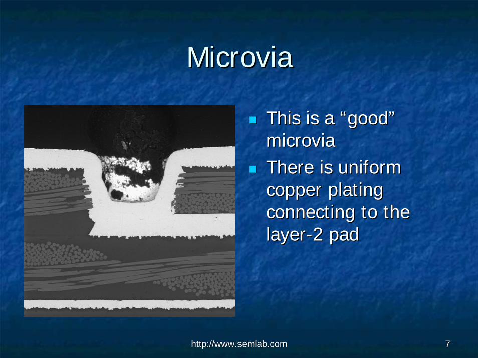
MicroviaMicrovia
This is a “good” This is a “good” microviamicroviaThere is uniform There is uniform copper plating copper plating connecting to the connecting to the layerlayer--2 pad2 pad

http://www.semlab.comhttp://www.semlab.com 88
What is this?What is this?

http://www.semlab.comhttp://www.semlab.com 99
Drill BreakoutDrill Breakout
The inner layer lands The inner layer lands probably should have probably should have been larger diameter been larger diameter in this designin this designThis condition fails This condition fails Class 3 criteria in IPCClass 3 criteria in IPC--AA--600 (min. annular 600 (min. annular ring 0.001 in)ring 0.001 in)

http://www.semlab.comhttp://www.semlab.com 1010
What is this?What is this?

http://www.semlab.comhttp://www.semlab.com 1111
EOS FailureEOS Failure
All four All four VccVcc wire wire bonds are fused openbonds are fused openThere is no damage There is no damage on the dieon the dieExcessive current Excessive current failure likely due to failure likely due to latchlatch--upup

http://www.semlab.comhttp://www.semlab.com 1212
EOS FailureEOS Failure
VccVcc wire bond is wire bond is fused openfused openFusing current of 1Fusing current of 1--mil gold wire is ~ mil gold wire is ~ 0.75 amps0.75 amps

http://www.semlab.comhttp://www.semlab.com 1313
EOS FailureEOS Failure
A short segment ofA short segment ofmetallizationmetallization was was fused open fused open Likely caused by a Likely caused by a voltage transientvoltage transient

http://www.semlab.comhttp://www.semlab.com 1414
EOS FailureEOS Failure
A short segment ofA short segment ofmetallizationmetallization was was fused open fused open Likely caused by a Likely caused by a voltage transientvoltage transient

http://www.semlab.comhttp://www.semlab.com 1515
EOS FailureEOS Failure
A short segment ofA short segment ofmetallizationmetallization was was fused open fused open Likely caused by a Likely caused by a voltage transient or voltage transient or ESDESD

http://www.semlab.comhttp://www.semlab.com 1616
EOS FailureEOS Failure
Gross electrical Gross electrical overstress damage overstress damage

http://www.semlab.comhttp://www.semlab.com 1717
What is this?What is this?

http://www.semlab.comhttp://www.semlab.com 1818
Bond Pad CorrosionBond Pad Corrosion
Contributing causes Contributing causes ––* moisture* moisture* * ““poppop--corncorn”” damagedamage* internal * internal delamdelam* P contamination* P contamination
http://www.semlab.comhttp://www.semlab.com 1919
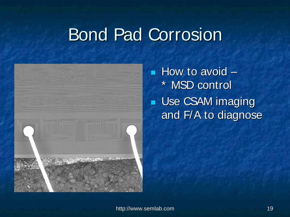
Bond Pad CorrosionBond Pad Corrosion
How to avoid How to avoid ––* MSD control* MSD controlUse CSAM imaging Use CSAM imaging and F/A to diagnoseand F/A to diagnose

http://www.semlab.comhttp://www.semlab.com 2020
Bond Pad CorrosionBond Pad Corrosion
Trace of PTrace of PP due to molding P due to molding compound or residual compound or residual from IC from IC fabfab

http://www.semlab.comhttp://www.semlab.com 2121
Bond Pad CorrosionBond Pad Corrosion
Bright spots are TiBright spots are Ti--W W barrier layer where Al barrier layer where Al is missingis missing

http://www.semlab.comhttp://www.semlab.com 2222
What is this?What is this?

http://www.semlab.comhttp://www.semlab.com 2323
DendriticDendritic Growth on IC DieGrowth on IC Die
Silver and copper Silver and copper dendritesdendritesFor all the same For all the same reasons as bond pad reasons as bond pad corrosioncorrosion

http://www.semlab.comhttp://www.semlab.com 2424
DendriticDendritic Growth on IC DieGrowth on IC Die
…… or most of the or most of the same reasons as bond same reasons as bond pad corrosionpad corrosion-- moisturemoisture-- ionic contaminationionic contamination-- biasbias-- internal internal delamdelam

http://www.semlab.comhttp://www.semlab.com 2525
What is this?What is this?

http://www.semlab.comhttp://www.semlab.com 2626
Bond Wire SweepBond Wire Sweep
Bond wires are swept Bond wires are swept by the injection by the injection molding compoundmolding compound

http://www.semlab.comhttp://www.semlab.com 2727
What is this?What is this?

http://www.semlab.comhttp://www.semlab.com 2828
Gold EmbrittlementGold Embrittlement
This is goldThis is gold--embrittledembrittledeutecticeutectic SnSn--PbPb soldersolderAuSn4 & AuSn2 AuSn4 & AuSn2 platelets dispersed platelets dispersed throughout the throughout the microstructuremicrostructure

http://www.semlab.comhttp://www.semlab.com 2929
Gold EmbrittlementGold Embrittlement
Theory Theory –– the goldthe gold--embrittlementembrittlement caused caused voiding!voiding!AuSn4 & AuSn2 AuSn4 & AuSn2 platelets trap volatilesplatelets trap volatiles

http://www.semlab.comhttp://www.semlab.com 3030
Gold EmbrittlementGold Embrittlement
Theory Theory –– the goldthe gold--embrittlementembrittlement caused caused voiding!voiding!AuSn4 & AuSn2 AuSn4 & AuSn2 platelets trap volatilesplatelets trap volatiles

http://www.semlab.comhttp://www.semlab.com 3131
What is this?What is this?

http://www.semlab.comhttp://www.semlab.com 3232
BGA Mechanical DamageBGA Mechanical Damage
Probably tool damageProbably tool damageMost extreme cases Most extreme cases had missing ballshad missing balls

http://www.semlab.comhttp://www.semlab.com 3333
BGA Mechanical DamageBGA Mechanical Damage
Corner has a missing Corner has a missing ball ball

http://www.semlab.comhttp://www.semlab.com 3434
What is this?What is this?
http://www.semlab.comhttp://www.semlab.com 3535
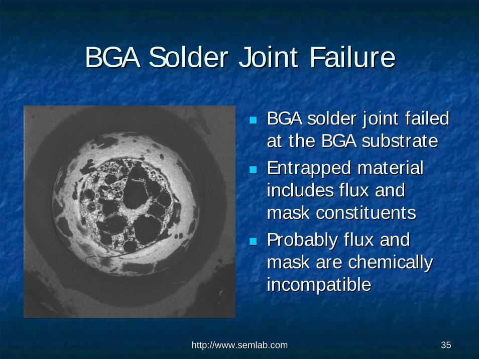
BGA Solder Joint FailureBGA Solder Joint Failure
BGA solder joint failed BGA solder joint failed at the BGA substrateat the BGA substrateEntrapped material Entrapped material includes flux and includes flux and mask constituentsmask constituentsProbably flux and Probably flux and mask are chemically mask are chemically incompatibleincompatible

http://www.semlab.comhttp://www.semlab.com 3636
BGA Solder Joint FailureBGA Solder Joint Failure
This is a different This is a different exampleexampleEntrapped material Entrapped material likely debris from likely debris from plastic traysplastic trays
http://www.semlab.comhttp://www.semlab.com 3737
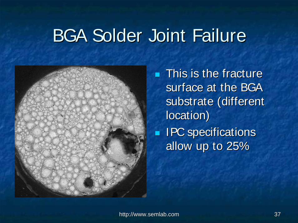
BGA Solder Joint FailureBGA Solder Joint Failure
This is the fracture This is the fracture surface at the BGA surface at the BGA substrate (different substrate (different location)location)IPC specifications IPC specifications allow up to 25%allow up to 25%

http://www.semlab.comhttp://www.semlab.com 3838
What is this?What is this?

http://www.semlab.comhttp://www.semlab.com 3939
ENIG Black Pad SyndromeENIG Black Pad Syndrome
Brittle fracture at the Brittle fracture at the solder/PWB pad solder/PWB pad interfaceinterfaceMore specifically More specifically between the Ni3Sn4 between the Ni3Sn4 IMC layer and the PIMC layer and the P--rich ENrich EN

http://www.semlab.comhttp://www.semlab.com 4040
ENIG Black Pad SyndromeENIG Black Pad Syndrome
Very fine line brittle Very fine line brittle fracture at the fracture at the solder/PWB pad solder/PWB pad interfaceinterface
http://www.semlab.comhttp://www.semlab.com 4141
ENIG Black Pad SyndromeENIG Black Pad Syndrome
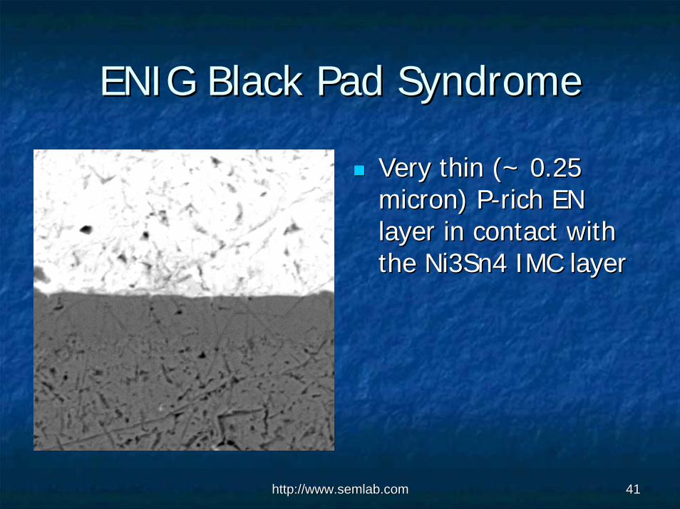
Very thin (~ 0.25 Very thin (~ 0.25 micron) Pmicron) P--rich EN rich EN layer in contact with layer in contact with the Ni3Sn4 IMC layerthe Ni3Sn4 IMC layer
http://www.semlab.comhttp://www.semlab.com 4242
ENIG Black Pad SyndromeENIG Black Pad Syndrome
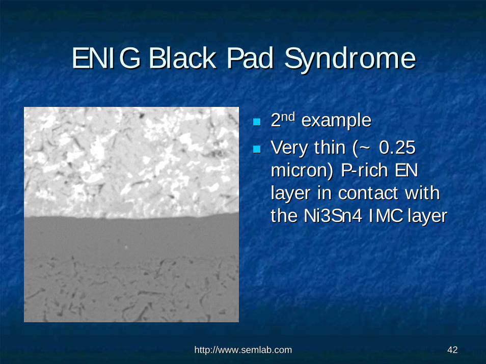
22ndnd exampleexampleVery thin (~ 0.25 Very thin (~ 0.25 micron) Pmicron) P--rich EN rich EN layer in contact with layer in contact with the Ni3Sn4 IMC layerthe Ni3Sn4 IMC layer
http://www.semlab.comhttp://www.semlab.com 4343
ENIG Black Pad SyndromeENIG Black Pad Syndrome
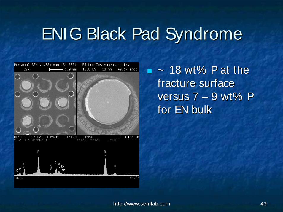
~ 18 wt% P at the ~ 18 wt% P at the fracture surface fracture surface versus 7 versus 7 –– 9 wt% P 9 wt% P for EN bulkfor EN bulk

http://www.semlab.comhttp://www.semlab.com 4444
ENIG Black Pad SyndromeENIG Black Pad Syndrome
IG spikingIG spikingHyperHyper--etching of EN etching of EN in IG bathin IG bath

http://www.semlab.comhttp://www.semlab.com 4545
ENIG Black Pad SyndromeENIG Black Pad Syndrome
22ndnd exampleexampleIG spikingIG spikingHyperHyper--etching of EN etching of EN in IG bathin IG bath

http://www.semlab.comhttp://www.semlab.com 4646
What is this?What is this?

http://www.semlab.comhttp://www.semlab.com 4747
Failed SMD InductorFailed SMD Inductor
Discoloration of Discoloration of magnet wiremagnet wireOpen circuited coilOpen circuited coil

http://www.semlab.comhttp://www.semlab.com 4848
Failed SMD InductorFailed SMD Inductor
EncapsulantEncapsulant voids voids around magnet wirearound magnet wireMagnet wire crossMagnet wire cross--section reduced due section reduced due to corrosionto corrosion

http://www.semlab.comhttp://www.semlab.com 4949
Failed SMD InductorFailed SMD Inductor
Corrosion due toCorrosion due to ClCl & & Br from activated flux Br from activated flux that wicked into the that wicked into the coilcoil

http://www.semlab.comhttp://www.semlab.com 5050
Failed SMD InductorFailed SMD Inductor
Corrosion due toCorrosion due to ClCl & & Br from activated flux Br from activated flux that wicked into the that wicked into the coilcoil

http://www.semlab.comhttp://www.semlab.com 5151
What is this?What is this?

http://www.semlab.comhttp://www.semlab.com 5252
Failed Resistor Network JointFailed Resistor Network Joint
Classic thermal Classic thermal fatigue failurefatigue failureVoids may be a Voids may be a contributing factorcontributing factor

http://www.semlab.comhttp://www.semlab.com 5353
Failed Resistor Network JointsFailed Resistor Network Joints
Classic thermal Classic thermal fatigue failurefatigue failureThermal expansion Thermal expansion mismatch too largemismatch too largeFailed after ~ 5 years Failed after ~ 5 years of serviceof service

http://www.semlab.comhttp://www.semlab.com 5454
What is this?What is this?

http://www.semlab.comhttp://www.semlab.com 5555
MLCC Knit Line FailureMLCC Knit Line Failure
MLCC manufacturing MLCC manufacturing defectdefectCrack propagates and Crack propagates and crosses plates causingcrosses plates causingelectromigrationelectromigration shortshort

http://www.semlab.comhttp://www.semlab.com 5656
MLCC Knit Line FailureMLCC Knit Line Failure
DelaminationDelamination between between plate and dielectricplate and dielectric

http://www.semlab.comhttp://www.semlab.com 5757
MLCC Dielectric VoidsMLCC Dielectric Voids
Void bridges plates Void bridges plates and createsand createselectromigrationelectromigration pathpath

http://www.semlab.comhttp://www.semlab.com 5858
MLCC Dielectric VoidsMLCC Dielectric Voids
Another example of Another example of MLCC dielectric voidsMLCC dielectric voids

http://www.semlab.comhttp://www.semlab.com 5959
What is this?What is this?
http://www.semlab.comhttp://www.semlab.com 6060
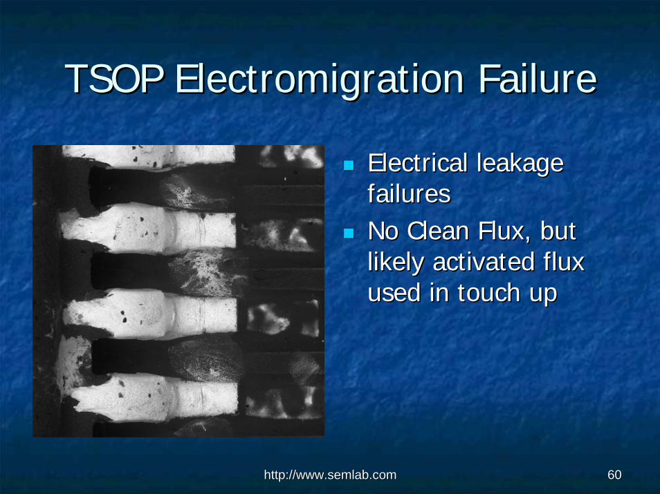
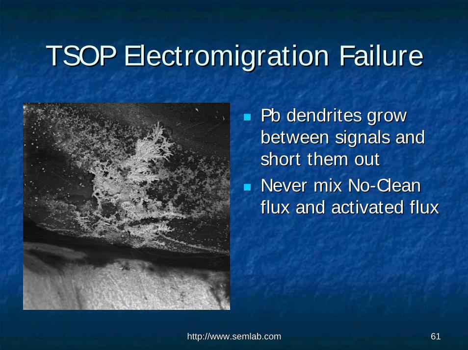
TSOP Electromigration FailureTSOP Electromigration Failure
Electrical leakage Electrical leakage failuresfailuresNo Clean Flux, but No Clean Flux, but likely activated flux likely activated flux used in touch upused in touch up
http://www.semlab.comhttp://www.semlab.com 6161
TSOP Electromigration FailureTSOP Electromigration Failure
PbPb dendrites grow dendrites grow between signals and between signals and short them outshort them outNever mix NoNever mix No--Clean Clean flux and activated fluxflux and activated flux

http://www.semlab.comhttp://www.semlab.com 6262
TSOP Electromigration FailureTSOP Electromigration Failure
Its even growing Its even growing across the mold flash across the mold flash up by the package up by the package body!body!

http://www.semlab.comhttp://www.semlab.com 6363
TSOP Electromigration FailureTSOP Electromigration Failure
There is nothing quite There is nothing quite like a pretty picture of like a pretty picture of aa PbPb--dendritedendrite

http://www.semlab.comhttp://www.semlab.com 6464
CONCLUSIONSCONCLUSIONS
Dendrites? Go ahead, make my day …Dendrites? Go ahead, make my day …Bond pad corrosion? Bring it on!Bond pad corrosion? Bring it on!Black pad syndrome? Not a HASLBlack pad syndrome? Not a HASL
Ed Hare, Ph.D./Ed Hare, Ph.D./SEM Lab, Inc.SEM Lab, Inc.