image processing using one-dimensional processor...
TRANSCRIPT
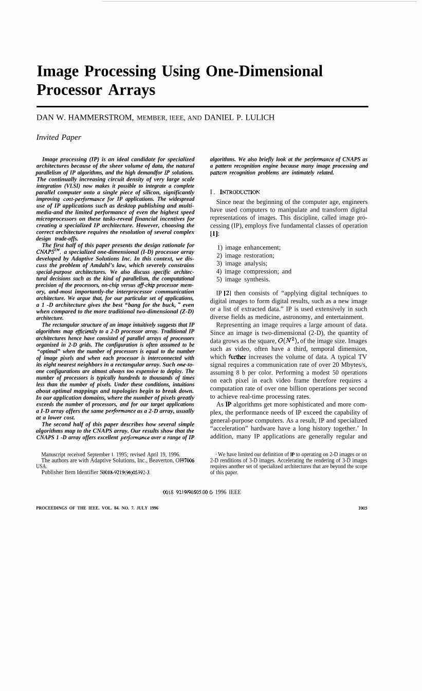
Image Processing Using One-DimensionalProcessor ArraysDAN W. HAMMERSTROM, MEMBER, IEEE, AND DANIEL P. LULICH
Invited Paper
Image processing (IP) is an ideal candidate for specializedarchitectures because of the sheer volume of data, the naturalparallelism of IP algorithms, and the high demandfor IP solutions.The continually increasing circuit density of very large scaleintegration (VLSI) now makes it possible to integrate a completeparallel computer onto a single piece of silicon, significantlyimproving cost-pelfonnance for IP applications. The widespreaduse of IP applications such as desktop publishing and multi-media-and the limited performance of even the highest speedmicroprocessors on these tasks-reveal financial incentives forcreating a specialized IP architecture. However, choosing thecorrect architecture requires the resolution of several complexdesign trade-offs.
The first half of this paper presents the design rationale forCNAPSTM, a specialized one-dimensional (I-D) processor arraydeveloped by Adaptive Solutions Inc. In this context, we dis-cuss the problem of Amdahl’s law, which severely constrainsspecial-purpose architectures. We also discuss specific architec-tural decisions such as the kind of parallelism, the computationalprecision of the processors, on-chip versus off-chip processor mem-ory, and-most importantly-the interprocessor communicationarchitecture. We argue that, for our particular set of applications,a 1 -D architecture gives the best “bang for the buck, ” evenwhen compared to the more traditional two-dimensional (Z-D)architecture.
The rectangular structure of an image intuitively suggests that IPalgorithms map eficiently to a 2-D processor array. Traditional IParchitectures hence have consisted of parallel arrays of processorsorganized in 2-D grids. The configuration is often assumed to be“optimal” when the number of processors is equal to the numberof image pixels and when each processor is interconnected withits eight nearest neighbors in a rectangular array. Such one-to-one configurations are almost always too expensive to deploy. Thenumber of processors is typically hundreds to thousands of timesless than the number of pixels. Under these conditions, intuitionsabout optimal mappings and topologies begin to break down.In our application domains, where the number of pixels greatlyexceeds the number of processors, and for our target applicationsa I-D array offers the same pegormance as a 2-D array, usuallyat a lower cost.
The second half of this paper describes how several simplealgorithms map to the CNAPS array. Our results show that theCNAPS 1 -D array offers excellent pelformance over a range of IP
Manuscript received September 1, 1995; revised April 19, 1996.The authors are with Adaptive Solutions, Inc., Beaverton, OR 97006
USA.Publisher Item Identifier S Oolg-9219(96)05392-3.
algorithms. We also briefly look at the per$ormance of CNAPS asa pattern recognition engine because many image processing andpanem recognition problems are intimately related.
I . INTRODU~~N
Since near the beginning of the computer age, engineershave used computers to manipulate and transform digitalrepresentations of images. This discipline, called image pro-cessing (IP), employs five fundamental classes of operationUl:
1) image enhancement;2) image restoration;3) image analysis;4) image compression; and5) image synthesis.
IP [2] then consists of “applying digital techniques todigital images to form digital results, such as a new imageor a list of extracted data.” IP is used extensively in suchdiverse fields as medicine, astronomy, and entertainment.
Representing an image requires a large amount of data.Since an image is two-dimensional (2-D), the quantity ofdata grows as the square, O(N*), of the image size. Imagessuch as video, often have a third, temporal dimension,which further increases the volume of data. A typical TVsignal requires a communication rate of over 20 Mbytes/s,assuming 8 b per color. Performing a modest 50 operationson each pixel in each video frame therefore requires acomputation rate of over one billion operations per secondto achieve real-time processing rates.
As IP algorithms get more sophisticated and more com-plex, the performance needs of IP exceed the capability ofgeneral-purpose computers. As a result, IP and specialized“acceleration” hardware have a long history together.’ Inaddition, many IP applications are generally regular and
’ We have limited our definition of IP to operating on 2-D images or on2-D renditions of 3-D images. Accelerating the rendering of 3-D imagesrequires another set of specialized architectures that are beyond the scopeof this paper.
OO1&9219/96$OSOO 0 1996 IEEE
PROCEEDINGS OF THE IEEE. VOL. 84. NO. 7. JULY 1996 1005
therefore relatively easy to parallelize.2 IP is a naturaldata parallel problem because it involves applying manyidentical, independent operations to an array of data, Thisregularity in the problem lends itself to regular computer ar-chitectures, which are similarly straightforward to build andprogram. IP and specialized hardware therefore also havea long future together, especially because IP is becomingmore common in large markets such as desktop publishing,multimedia, and image recognition.
As the requirements for image processing have increased,so have the capabilities of integrated circuit technology.The ability to integrate large numbers of transistors ontoone piece of silicon and operate them at a very highfrequency has increased at a constant rate over the last20-30 years. This increase, often called Moore’s Law,was formulated by Gordon Moore, one of the foundersof Intel Corporation [3]. Moore’s law states that siliconperformance and density roughly double every 1.5 years.This continuing increase in silicon performance (coupledto decreases in implementation cost) motivated us to createcustom silicon devices for accelerating IP and the relatedfunction of pattern recognition. The result of our designefforts is the CNAPS architecture and chip set.
The designer of a high-performance chip architecturemust consider some serious pitfalls including the dev-astating effects of Amdahl’s law [4], cost-performancetrade-offs, and the appropriate range of functionality. Wedo not claim to have made the correct decision in all cases,and some decisions had better results than others. But wedo feel that a discussion of the design rationale and of theapplications used by the resulting architecture would be ofinterest to those who work in IP and beyond.
This paper has two major parts. The first describesthe CNAPSTM architecture and the design rationale forits major features. This discussion concentrates on theinterprocessor communication design, since that topic offersinsight into building large VLSI-based arrays of parallelprocessors. The second part describes some real-world ap-plications that use CNAPS to show how these applicationsmap to the architecture.
I I . CNAPS A R C H I T E CT U R E- DESIGN R A T I O N A L E
One goal of CNAPS was to exploit the data parallelismof IP to give a significant cost-performance advantageover existing high-speed microprocessor technology (“killermicros”). Another goal was to make CNAPS fairly easyto program and flexible enough to support a fairly widerange of algorithms. In addition, we wanted it to be small,compact, and inexpensive so that an entire IP engine couldfit on one PC card for desktop applications.
The first problem a designer of special-purpose com-puters runs into is Amdahl’s Law.s When parallelizing anapplication, Amdahl says that the part of the application that
aThis parallelism has been leveraged in several image processingarchitectures from systolic pipelines to parallel processor arrays. The latterwill be the primary focus of this article.
3Amdahl’s law [4] states simply that an application is only as fast asits slowest component.
(1 O* opskec)
l flexible digital (10’)
0 specialized digital
\(10’0)
. analog(10”)
performance/cost (log scale)
Fig. 1. “Flexibility” versus cost-performance.
is not sped up dominates the total speed-up possible. Forexample, suppose that you have invented a new special-purpose chip that can speed up part of an applicationup by a factor of 1000. As often happens, the portionof the application your chip accelerate accounts for onlya small part of the total application’s cycles, say 30%.Consequently, the total application is sped up only by 30%.Unless your new chip is inexpensive and easy to program,few customers will use it, since by the time they port theirapplications to it, general-purpose processors will be 30%faster anyhow. IP is one of the few areas where specializedarchitectures can compete with “killer micros” in spite ofAmdahl’s law, mainly because IP algorithms have a highdegree of natural parallelism that makes it relatively easyto create powerful, economical IP engines. Nevertheless,the designer of an IP engine for use with general-purposeapplications must be .aware of Amdahl’s law.
The CNAPS solution to Amdahl’s law was two-fold. Thefirst objective was to find a specific set of applications thatshare similar computational characteristics and optimize thearchitecture for these and nothing else. We make no claimsthat CNAPS is a general-purpose machine. It was designedfor IP and pattern recognition (PR).
The second objective was to create an architecture thatwas as flexible as possible within the general performanceobjectives needed for our target markets, another strongargument for a programmable architecture. Fig. 1 demon-strates this trade-off. The horizontal dimension indicatescost-performance,4 usually measured in operations/secondper dollar. The vertical dimension is more subjective, butdescribes a “flexibility” measure. Although it is difficultto quantify, computer architects agree that there is a cleartrade-off between flexibility and performance. When youdesign a chip for a specific application, you can leveragesignificant parallel opportunities and forego certain kindsof computation, thus allowing a higher cost-performancethan a general-purpose machine that must do everything.Through the middle of the figure is the “technology barrier,”which moves to the right over time. The technology banier
4We use the colloquial term “cost-performance” to mean performancedivided by cost.
1006 PROCEEDINGS OF THE IEEE. VOL. 84. NO. 7. JULY 1996
results from practical issues: you can put only so manytransistors on a chip, they cost so much, and can performonly so much computational work. At the left end of thespectrum are the latest generations of general-purpose pro-cessors (i.e., the Intel PentiumTM), which give reasonablecost-performance over a wide range of applications. At theother end are the very specialized devices, often built toexecute a single function (i.e., a modem chip).
Flexibility is extremely important, because even a simplepattern recognition application must execute a fairly broadrange of algorithms. Amdahl tells us that the total systemspeed up is proportional to the percentage of algorithms thatwe cannot map to our specialized processor-that is, thosealgorithms that must be executed by the host. So exceptfor certain high-volume, very specialized chips, Amdahltends to push specialized architectures to the left end ofthe scale. An architecture that is too close to the general-purpose processors in cost-performance cannot competewith them. The trick when designing CNAPS was to createenough flexibility to avoid the perils of Amdahl’s law, yethave a sufficiently superior cost-performance over existingmicroprocessor technology to justify its cost in a system.
The next few sections highlight and justify the majorarchitecture decisions in light of the above reasoning.
A. SIMD ParallelismMost parallel computer architectures fall into two broad
categories: multiple instruction stream multiple data stream(MI&ID) and single instruction stream and single datastream (SIMD) [5]. In M&ID-parallel machines, each arith-metic logic unit (ALU) unit has its own, independentinstruction sequencer. Each ALU therefore can act inde-pendently. In SIMD-parallel machines, all ALU’s share onesequencer. Each ALU therefore does the same thing at thesame time, but on a different piece of data. SIMD compu-tation is often called data parallelism. MIMD is generallymore powerful and flexible than SIMD, but SIMD is lessexpensive. SIMD is also much easier to program becauseit has one thread of control. MIMD, on the other hand,has multiple, interacting, relatively asynchronous controlthreads, greatly complicating the programming model.
Almost all custom IP architectures have been SIMD,since IP is very much a data parallel problem [5]. Wedecided to use SIMD parallelism for the same reasons: ourtarget algorithms consisted of performing the same opera-tion, in parallel, over many pieces of data in large, arrayedcomputing structures. We were also attracted to the simplerprogramming model and to the favorable cost-performanceachieved through a simple restriction in functionality.
So our first decision was to obtain the needed perfor-mance by exploiting the inherent data parallelism in thealgorithms used in our target applications, and to implementthis parallelism in a SIMD design. Our machine wouldconsist of an array of processor nodes (PN’s)~ operatingin lock-step synchrony and controlled by one instruction
‘For historical reasons, we use the term processor node (PN) instead ofthe traditional SIMD term processor element (PE).
sequence unit. As with all SIMD architectures, the PN’swould be able to conditionally execute an instruction basedon some internal logical condition (for example, adderoutput equal to zero, or negative).
B. Arithmetic PrecisionThe next major architectural question concerned the
representation of the data computed by each PN. Thealternatives here broadly range from bit-serial to full bit-parallel floating point. Bit-serial representation means thateach bit of an arithmetic operation is computed one bit at atime. A fixed-point add of 72 bits thus requires O(n) clocks,and a multiply requires O(n*) clocks. Bit-serialism thusallows arbitrary precision (just use more clocks), which isuseful in many IP problems. Bit-serial PN’s are extremelysimple, so many PN’s can be placed in one chip. Inter-PNinterconnect likewise tends to be serial.
Bit-parallel designs, on the other hand, can perform entireadds or multiplies in one clock cycle. This bit-parallelarithmetic tends to be easier to program and faster than bit-serial arithmetic. A drawback is that bit-parallel PN’s areharder to design than bit-serial PN’s and also require moresilicon area.6 In addition to “pure” bit-serial or bit-paralleldesigns, there are also a range of intermediate designs.For example, an ALU could do 4-b arithmetic with theprogrammer doing higher precision fixed-point operationsby serially combining 4-b operations.
All of these options lead to different siliconspace/computation time trade-offs. We decided toimplement bit-parallel arithmetic because it is easierto program and faster for higher precision. The nextquestion was whether to use a fixed-point (where theprogrammer statically manages the radix point) or afloating-point representation (where the machine itselfdynamically manages the radix point). Floating point ismuch easier for programmers to use and generally hasbetter arithmetic characteristics such as greater precisionand dynamic range. Unfortunately, floating point isexpensive, since it requires hardware to perform thevarious shifting and normalization operations, exponentarithmetic, and bit truncation (usually rounding).
For CNAPS, floating point had an additional expense.Our PN’s were small enough to use PN redundancy to im-prove semiconductor yield (the number of good dice-thatis, chips-per wafer), much like the way many memorymanufacturers use extra columns and rows to replace faultyrows or columns. Due to the current defect density ratesof silicon processes, the use of redundant componentscan significantly improve yield. It works only if the unitof redundancy is small, the exact size being a complexfunction of the percentage of nonredundant circuitry (suchas global interconnect) and the defect density per unit of
6The cost of a chip is generally proportional to its size, since siliconwafers have a fixed cost, and the number of finished chips per waferdepends on the size of the chip. Chip size and wafer yield have a complex.nonlinear relationship, not only do bigger chips take up more space on thewafer, but also each chip is more likely to fail due to manufacturingdefects.
HAMMERSTROM AND LULICH: IMAGE PROCESSING USING ONE-DIMENSIONAL PROCESSOR ARRAYS 1007
wafer area. In our analysis, a 32-b floating-point PN wasroughly three to four times larger than the 8116-b fixed-point PN we used,l assuming that we implemented theIEEE floating-point standard. This analysis showed thatthe floating-point PN was too large to effectively employredundancy, but the smaller 8/16-b PN could do so anddouble the yield. Extensive simulation showed that theproblem domains we have targeted, such as IP, can operatequite effectively at 8 and 16-b precision.
C. Processor Memory ArchitectureAs the PN’s compute, they need input data to compute
with. In most IP applications, the multiply-accumulate(MAC) operation dominates, which requires two inputoperands per clock. In most of our computations, the PN’scan share one of those operands, but the other is uniqueto each PN. The question then is, where are these uniqueoperands stored, and how are they moved to each PN’sarithmetic unit? The two general techniques are on-chipstorage and off-chip storage.
Storing operands off-chip requires moving them onto thechip and into each PN during computation, which in turnrequires a separate, independent pathway from an off-chipmemory to each PN. An advantage is that each PN canhave essentially unlimited memory space, implemented incommercially available memory. A drawback is that thelimited bandwidth going on and off the chip (the maximumnumber of pins, their maximum switching rate, and theirpower consumption) imposes limits on the speed and/ornumber of PN’s on the chip. Likewise, due to off-chipbandwidth limitations, off-chip memory systems generallyuse a single address for all PN memory-that is, each PNmust access the same location as its brethren.
The other technique is to put a memory next to eachPN. One advantage is reducing the off-chip circuitry, pins,and power dissipation. Another is that each PN can nowhave one clock access to its own local memory, andeach PN can access a different location, allowing morecomplex functionality such as table lookup and per PNindirect addressing. The big disadvantages are the expense,in silicon area, of the memory, and limitations on the totalamount of memory available.
The memory design was one of the most complex ar-chitecture decisions, since both techniques had comparableadvantages and disadvantages. Several factors influencedour final decision to use on-chip per-PN memory. Theprimary influence was the silicon capability available tous. We were able to use a commercial SRAM processthat permitted a large number of dense memory cells onthe chip. The first version of the CNAPS architecture wasfabricated in a 0.8 pm CMOS SRAM process with fourlayers of metal and two layer polysilicon. The SRAM cellwas 47 pm’, using four transistors (with poly load pull
‘lr is possible to have a 16-b Roatinp-point number, but it is usefulonly for a limited range of algorithms. For a commercial product, we feltthat any floating point representation would have to be the one thar peopleare used to using. The analysis therefore assumed 32-b IEEE standardrepresentation. with an 8-b exponent and 24-b mantissa.
1008
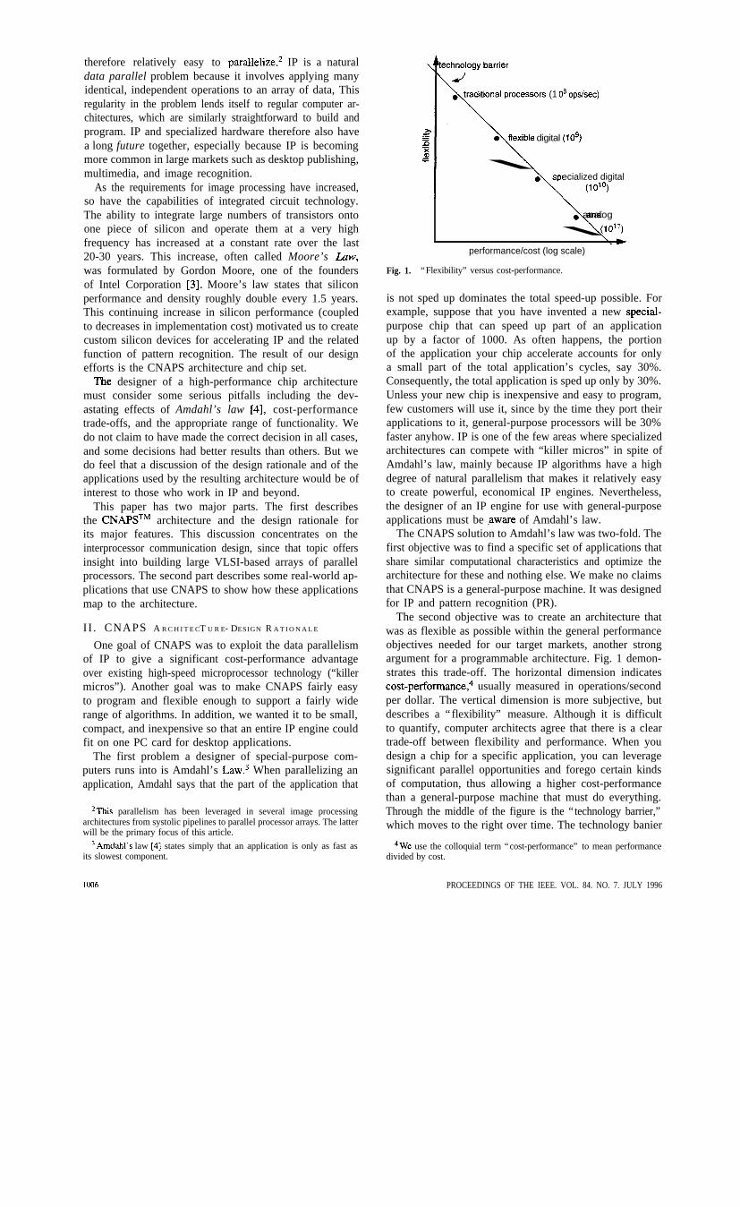
2D:
Fig. 2. I-D and 2-D processor arrays. Each “chip” has 64 pro-cessors.
ups). The second capability was using redundant com-ponents via a proprietary laser fusing technology. Thisredundancy-developed independently for memory prod-ucts-coupled with the ability to stitch together multiplemask exposures, let us build a single, large die. The firstCNAPS implementation had 64 working PN’s on a singlechip: 80 were fabricated in a 8 x 10 array, leaving 16spare for redundancy. This level of integration preventedthe use of off-chip memory, but it permitted significanteconomies of scale, lowering the price per PN. So the finaldecision was between limited (on-chip) memory per PN,but low per PN cost, or unlimited (off-chip) memory perPN, but high PN cost. We analyzed the mapping of severalalgorithms to the architecture, such as those shown in thesecond half of this paper. This analysis is not repeated here,but our conclusion was that the algorithms could adequatelyexecute within a 4 KB PN memory. In retrospect, 4 KB perPN was a sufficiently large “local programmable cache”for a broad range of IP and PR algorithms, even thoughsome applications (general speech recognition being one ofthe most prominent) could not use CNAPS due to memoryconstraints.
D. Inter-processor Communication ArchitectureThe next major decision was how to connect the PN’s
to each other. Over the years, several interconnectionarchitectures have been developed for parallel processorarrays [5]. Choosing the wrong interconnection architecturecould severely impact the cost-performance of CNAPS. Instudying our target applications, we realized that they in-volved almost exclusively global and local communication.We concluded that providing efficient global, intermediate,and local communication was too expensive, so we decidedto provide local and global connectivity.
In our target applications, the global interconnect patternswe looked at were dominated by “one to many” and “manyto many” style communication. The most efficient wayto perform this type of communication is with a simplebroadcast bus connecting all PN’s. The sequential broadcastof data allows us to perform 0(n2) communication in O(n)clocks. Broadcast is inefficient, however, when loadingper-PN data (such as filling PN memories) because each
PROCEEDINGS OF THE IEEE. VOL. 84. NO. 7. JULY 1996
chip does not have enough pins to give each PN its ownpath to memory. Our solution was to use “multiple tappedbroadcast,” where a tap can broadcast to a subset of PN’s,with each tap broadcasting in parallel to its subset. The topof Fig. 2 shows a 1-D array architecture of four chips witha single I/O “tap” per chip. The current implementation ofCNAPS offers one tap per chip, which in multichip systemsmatches the bandwidth of most buses.
We use multiple taps in our 1-D architecture to increasethe ratio of external chip UO paths to PN’s. Today’ssilicon technology provides a particular ratio of pin count(proportional to the length of the chip periphery) to the areafor internal logic. These silicon area and power limitationsultimately constrain the ratio of I/O per PN. A 1-D archi-tecture generally has too low a ratio, thereby not effectivelyusing the available I/O capabilities. As we will show below,a 2-D architecture actually has too high a ratio. So, thoughit is also possible to add multiple taps to a 2-D array, doingso would increase what is already too high of a ratio ofI/O to compute.
For outputting data, we have a single “broadcast” likeoutput bus, the OutBus, that allows simultaneous or in-dividual transmission. Several arbitration techniques areavailable to guarantee that only one PN is using theOutBus at a time. When simultaneous output from twoor more PN’s, the OutBus performs a logical AND ofthe various PN’s outputs. This lets CNAPS perform globallogic operations across all PN’s.
The next issue concerned how to support local inter-PNcommunication, where PN’s in a small neighborhood sharedata with each other. Over the years, several excellent IParchitectures have shown great flexibility and speed in theirtargeted applications [6], [7]. Probably the best example isMartin Marietta’s GAPP series [8], which uses a 2-D arrayof bit-serial processors.
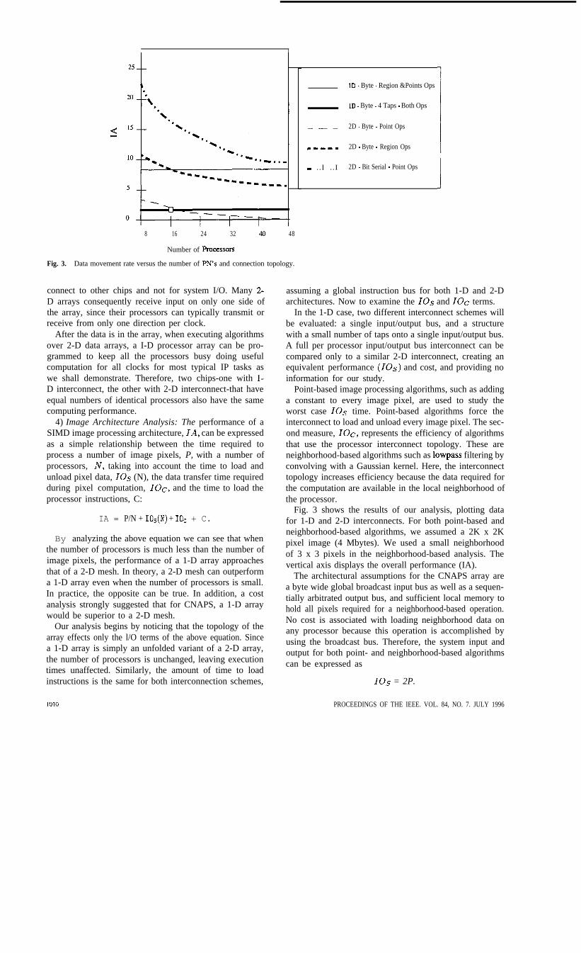
The GAPP and its brethren are 2-D architectures, de-signed to look like the data structures they compute over.Since images are 2-D, a 2-D grid structure lets the IP pro-grammer assign one processor to each pixel, or to a squareor rectangular group of pixels. However, as we progressto higher-density VLSI implementations, 2-D structuresstart to become unwieldy to implement. Consequently,there have been some 1-D IP architectures [9], [lo] thathave been proposed through the years. Fig. 2 shows someexamples of 1-D and 2-D arrays. We found through ouranalysis that in our IP and PR applications, we neededonly a 1-D structure. Since 1-D is cheaper and our goalwas build an effective and inexpensive image processingarchitecture, we came to the conclusion that for CNAPSand our target applications, the 1-D and 2-D architectureswith identical processors (same precision, storage, function,and speed) offered roughly the same performance, and the1-D case was cheaper to build because it used less siliconarea and off-chip bandwidth.
I) Scalability: The first problem with 2-D architecturesis scalability. In theory, 2-D grid structures are infinitelyscaleable; in practice, today’s VLSI technology imposesseveral limits [ll], the most serious being off-chip I/O
bandwidth, which is expensive in systems cost (pads, traces,packages) and in power dissipation (a growing problem inhigher-frequency computing). Consequently, scaling up thenumber of processors per chip makes the chip and systemmore expensive.
Several factors influence pin requirements. A 2-D chipwith an N x N array requires 4 x N x W pins, whereW is the word width A 1-D chip requires only 2W pins.In 2-D, adding processors (N) significantly increases thenumber of pins; in I-D, adding processors leaves the pincount unchanged. While it is sometimes possible to put theentire 2-D grid on one chip, our target applications requiredmore processors than one die can hold. In spite of the highlevel of VLSI integration, future applications are likely tocontinue to use multichip processor arrays for some time.
As on-chip clock frequencies get higher and higher-andthe difference between on-chip and off-chip frequenciesgets larger and larger-the word width grows to avoidbecoming a bottleneck. Increasing W adds yet more pins. Itis easy to see that 2-D arrays (4 x N x W) exhaust the pinlimits imposed by packaging technology long before 1-Darrays (2W) do. Therefore, as VLSI densities continue toscale, multichip 2-D grids reach bandwidth limits beforemultichip 1-D grids do.
A 2-D processor grid has on-chip costs as well. Eachprocessor must communicate with four (or eight in somecases) other processors, not with two, forcing additionalinternal silicon area to be dedicated to busing and control.In addition, a processor typically executes one operation ata time. Therefore, each processor normally can transfer datato only one neighbor per clock cycle. Each I-D processorhas essentially one external bus, which it can fully employat each clock. Each 2-D processor has two buses, so the2-D array generally underutilizes half of its potential extrabandwidth.
2) Redundancy: As discussed above, another cost issuewas our intended use of redundant processors. As siliconarea gets larger, the probability of a defect occurring ona chip gets rapidly larger. While the latest generation ofprocess technology has the lowest defect densities yet, de-fects are still present. Redundancy improves silicon yieldsby printing extra copies of certain circuits, then turningoff flawed copies in favor of good ones. Redundancy canrescue many dice that would be wasted otherwise 1121.Redundancy has its own cost and ultimately must “pay itsway.”
It is possible-but difficult and expensive-to employredundancy in a 2-D array. A 2-D design introduces ge-ometrical constraints that make it difficult to specify aredundancy mechanism that pays for itself by improvingyield enough to justify the extra silicon cost. With a l-D design it is possible to easily bypass any number ofprocessors (within electrical limits). A 1-D array can easilyuse redundancy to improve yield, decreasing the cost perfinished chip.
3) L/O Bandwidth: A 1-D system has much less I/Obandwidth than a 2-D system (2W pins versus 4 x N x Wpins). In a 2-D design many of those pins are used to
HAMMERSTROM AND LULICH: IMAGE PROCESSING USING ONE-DIMENSIONAL PROCESSOR ARRAYS 1009
1D - Byte - Region &Points Ops
1D - Byte - 4 Taps - Both Ops
--- 2D - Byte - Point Ops
1--1- 2D - Byte - Region Ops
I . . I . . I 2D - Bit Serial - Point Ops
8 16 24 32 40 48
Number of Processors
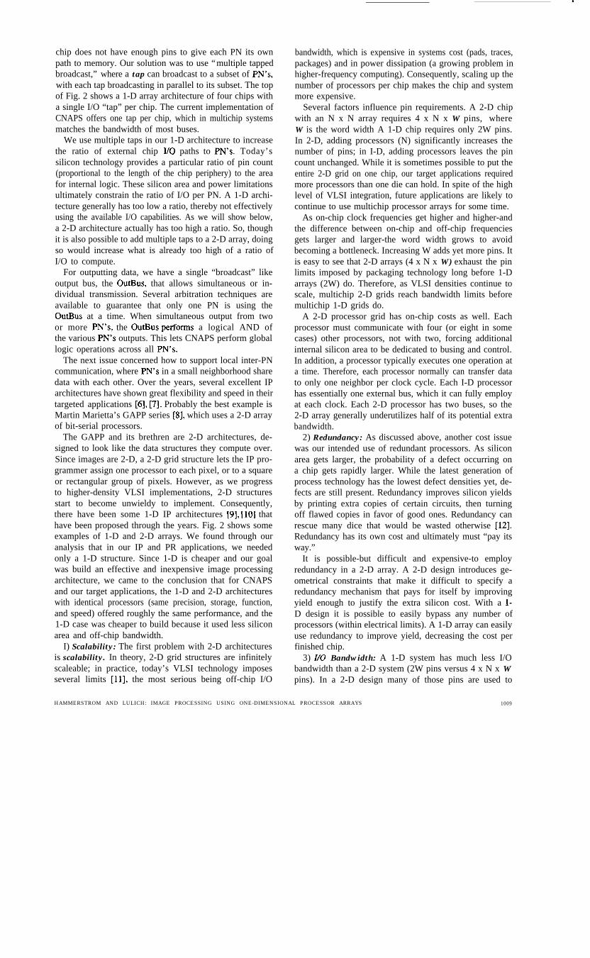
Fig. 3. Data movement rate versus the number of PN’s and connection topology.
connect to other chips and not for system I/O. Many 2-D arrays consequently receive input on only one side ofthe array, since their processors can typically transmit orreceive from only one direction per clock.
After the data is in the array, when executing algorithmsover 2-D data arrays, a I-D processor array can be pro-grammed to keep all the processors busy doing usefulcomputation for all clocks for most typical IP tasks aswe shall demonstrate. Therefore, two chips-one with l-D interconnect, the other with 2-D interconnect-that haveequal numbers of identical processors also have the samecomputing performance.
4) Image Architecture Analysis: The performance of aSIMD image processing architecture, IA, can be expressedas a simple relationship between the time required toprocess a number of image pixels, P, with a number ofprocessors, N, taking into account the time to load andunload pixel data, IOs (N), the data transfer time requiredduring pixel computation, IOc, and the time to load theprocessor instructions, C:
IA = P/N + I&(N) + IOc + C.
By analyzing the above equation we can see that whenthe number of processors is much less than the number ofimage pixels, the performance of a 1-D array approachesthat of a 2-D mesh. In theory, a 2-D mesh can outperforma 1-D array even when the number of processors is small.In practice, the opposite can be true. In addition, a costanalysis strongly suggested that for CNAPS, a 1-D arraywould be superior to a 2-D mesh.
Our analysis begins by noticing that the topology of thearray effects only the l/O terms of the above equation. Sincea 1-D array is simply an unfolded variant of a 2-D array,the number of processors is unchanged, leaving executiontimes unaffected. Similarly, the amount of time to loadinstructions is the same for both interconnection schemes,
IO10
assuming a global instruction bus for both 1-D and 2-Darchitectures. Now to examine the IOs and IOC terms.
In the 1-D case, two different interconnect schemes willbe evaluated: a single input/output bus, and a structurewith a small number of taps onto a single input/output bus.A full per processor input/output bus interconnect can becompared only to a similar 2-D interconnect, creating anequivalent performance (IOs) and cost, and providing noinformation for our study.
Point-based image processing algorithms, such as addinga constant to every image pixel, are used to study theworst case IOS time. Point-based algorithms force theinterconnect to load and unload every image pixel. The sec-ond measure, IOc, represents the efficiency of algorithmsthat use the processor interconnect topology. These areneighborhood-based algorithms such as lowpass filtering byconvolving with a Gaussian kernel. Here, the interconnecttopology increases efficiency because the data required forthe computation are available in the local neighborhood ofthe processor.
Fig. 3 shows the results of our analysis, plotting datafor 1-D and 2-D interconnects. For both point-based andneighborhood-based algorithms, we assumed a 2K x 2Kpixel image (4 Mbytes). We used a small neighborhoodof 3 x 3 pixels in the neighborhood-based analysis. Thevertical axis displays the overall performance (IA).
The architectural assumptions for the CNAPS array area byte wide global broadcast input bus as well as a sequen-tially arbitrated output bus, and sufficient local memory tohold all pixels required for a neighborhood-based operation.No cost is associated with loading neighborhood data onany processor because this operation is accomplished byusing the broadcast bus. Therefore, the system input andoutput for both point- and neighborhood-based algorithmscan be expressed as
IOS = 2P.
PROCEEDINGS OF THE IEEE. VOL. 84, NO. 7. JULY 1996
We also examined the case where the 1-D array hasmultiple taps on the I/O bus. Such taps enable a concurrentI/O capability that improves the overall IO performance asa function of the number of taps. The 1-D multitap l/O canbe compared Jo a 2-D mesh because it is simply a hybridI-D case, not a variant of a 2-D mesh. The 1-D hybrid lacksthe neighborhood topology of a 2-D array, but overcomesthis omission with the judicious use of local memory. Bothpoint-based and neighborhood-based algorithms use the l-D multitap tiay in the same way as the single I/O bus.Performance depends on the number of taps; we analyzeda 1-D array with four taps
Point-based algorithms do not benefit from the mesh con-nected topology of a 2-D array, but inpur and output muststill be performed. The number of point-based operationsfor a 2-D mesh where input and output occur along oneside of the array can be written as
IOS = 2%.Neighborhood-based algorithms take advantage of the 2-
D interconnect topology to improve IOC in two ways.First, multiple data paths improve input and output. Sec-ond, they also improve communications efficiency becausenearby processors can rapidly pass data required for thecomputation. The following equation expresses this kind ofcommunication efficiency and introduces a new term, R,which is the extent of the local neighborhood required forprocessing [ 131
IOc = [R2 - l+fi+2[R-I]];.
The last case examined, the bit-serial implementation ofthe 2-D mesh, shows the power of bit parallelism. Wideningthe bus to a one byte (8-b) width improves IOs by afactor of eight. Only the IOs performance of point-basedalgorithms is plotted. The IOC can be easily computed aseight times the L/O value of the 2-D neighborhood case.This value was not plotted because the performance alongmost of the curve was so slow that it was outside the scaleof the graph. The difference in performance between thebit-serial bus and byte wide bus is expressed as
IO.5=82 -5H 11Referring to Fig. 3, when the number of processors is
small, I-D arrays with a byte-wide input bus outperformbit-serial 2-D mesh implementations for both point- andneighborhood-based algorithms. Since bit-serial implemen-tations of the interconnect have so far been the typicalchoice for mesh connected architectures, our data show thatthe number of processors must exceed 48 to compete withI-D byte wide arrays.
Although point operations show improvement for smallnumbers of processors, a 1-D array is more efficient than
a 2-D array for neighborhood-based operations. Addingmore taps to a 1-D array further improves its efficiency.For example, a 16-processor 1-D system with four taps isequivalent to a 16-processor 2-D mesh where data is inputalong one side, as marked with a square on Fig. 3.
Notice that a 1-D multitap array is consistently more effi-cient for neighborhood-based algorithms for configurationsup to at least 48 processors. This advantage results fromthe 1 -D array having a global broadcast bus and using localmemory. When the number of processors exceeds 16, themultiple-tap broadcast8 architecture is roughly equivalentto 2-D, showing better performance in the neighborhood-based operations and slightly worse performance in thepoint-based operations. Without taking the cost of extra pinsinto account, it is easy to argue for the I-D architecture interms of communications performance. When the numberof processors is small and multiple taps can be employed,a I-D CNAPS array could offer equal-or in some casesbetter-performance than a 2-D bit-serial mesh.
To see why better performance is possible, consider thesituation where a column of pixels are stored in eachPN, and it processes the column one pixel at a time.Horizontal data transfer is required to obtain informationfrom neighboring columns on neighboring PN’s. Whenfetching data in the vertical dimension, however, the accessis essentially independent of the number of elements away,since it exists in the memory of the PN itself.
Using pin cost as a metric, we can strengthen ourargument by weighing our (IOs) performance equationsby the cost of additional pins. Let us look at the equationfor IOs for point-based operations using a 2-D mesh.We normalize this equation by the cost of the additionalinterconnect. Since we are inputting data via one side ofthe array, the 2-D mesh uses fi more pins than a 1-Dsingle bus array. We can state the meaning of this equationas input/output cycles per pin
IOs= 2-$ dR or IOs = 2p.
Upon simplification the performance per pin is exactlythe VO performance of the 1-D case per pin. This result isnot really surprising, but drives home the cost-performanceargument. Similar normalization can be performed for theremaining I/O equations-the result is the same.
Based on this analysis we concluded that a I-D CNAPSPN array was sufficient for our application space. We nextpresent a general discussion of the resulting architecture.We find it interesting that Jonker [ 141 recommended manyof our architectural decisions independently. His analysiscorroborates our choices of 1-D interconnect, byte, andwordwide buses and arithmetic units, and large local mem-ory for subimage caching.
‘Having too many taps makes it difficult to leverage redundancyeffectively even for a 1-D architecture. In CNAPS, we have found thatusing 16 PN’s between taps adds reasonable IOs performance, andredundancy within groups of 16 PN’s does not impact yield significantly.Also, as the number of taps increases. the inter-PN interconnect layoutcost starts to approach that of 2-D.
HAMMERSTROM AND LULICH: IMAGE PROCESSING USING ONE-DIMENSIONAL PROCESSOR ARRAYS 101 I
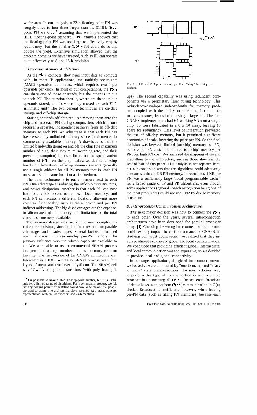
CNAPS 1 CNAPS 1
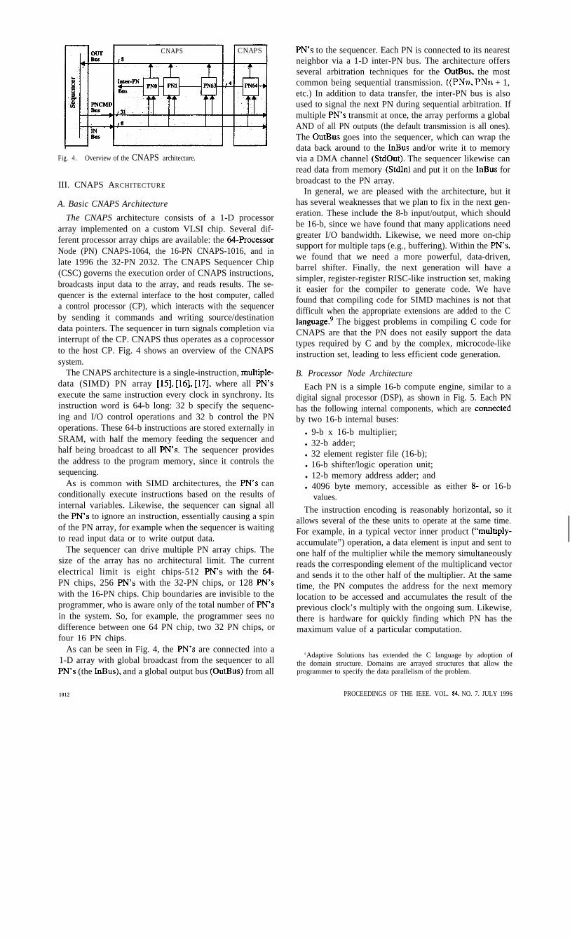
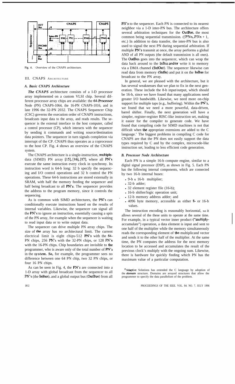
I IFig. 4. Overview of the CNAPS architecture.
III. CNAPS ARCHITECTURE
A. Basic CNAPS ArchitectureThe CNAPS architecture consists of a 1-D processor
array implemented on a custom VLSI chip. Several dif-ferent processor array chips are available: the 64ProcessorNode (PN) CNAPS-1064, the 16-PN CNAPS-1016, and inlate 1996 the 32-PN 2032. The CNAPS Sequencer Chip(CSC) governs the execution order of CNAPS instructions,broadcasts input data to the array, and reads results. The se-quencer is the external interface to the host computer, calleda control processor (CP), which interacts with the sequencerby sending it commands and writing source/destinationdata pointers. The sequencer in turn signals completion viainterrupt of the CP. CNAPS thus operates as a coprocessorto the host CP. Fig. 4 shows an overview of the CNAPSsystem.
The CNAPS architecture is a single-instruction, multiple-data (SIMD) PN array [15], [16], [17], where all PN’sexecute the same instruction every clock in synchrony. Itsinstruction word is 64-b long: 32 b specify the sequenc-ing and I/O control operations and 32 b control the PNoperations. These 64-b instructions are stored externally inSRAM, with half the memory feeding the sequencer andhalf being broadcast to all PN’s. The sequencer providesthe address to the program memory, since it controls thesequencing.
As is common with SIMD architectures, the PN’s canconditionally execute instructions based on the results ofinternal variables. Likewise, the sequencer can signal allthe PN’s to ignore an instruction, essentially causing a spinof the PN array, for example when the sequencer is waitingto read input data or to write output data.
The sequencer can drive multiple PN array chips. Thesize of the array has no architectural limit. The currentelectrical limit is eight chips-512 PN’s with the 64-PN chips, 256 PN’s with the 32-PN chips, or 128 PN’swith the 16-PN chips. Chip boundaries are invisible to theprogrammer, who is aware only of the total number of PN’sin the system. So, for example, the programmer sees nodifference between one 64 PN chip, two 32 PN chips, orfour 16 PN chips.
As can be seen in Fig. 4, the PN’s are connected into a1-D array with global broadcast from the sequencer to allPN’s (the InBus), and a global output bus (OutBus) from all
1012 PROCEEDINGS OF THE IEEE. VOL. 84, NO. 7. JULY 1996
PN’s to the sequencer. Each PN is connected to its nearestneighbor via a 1-D inter-PN bus. The architecture offersseveral arbitration techniques for the OutBus, the mostcommon being sequential transmission. ((PNn, PNn + 1,etc.) In addition to data transfer, the inter-PN bus is alsoused to signal the next PN during sequential arbitration. Ifmultiple PN’s transmit at once, the array performs a globalAND of all PN outputs (the default transmission is all ones).The OutBus goes into the sequencer, which can wrap thedata back around to the InBus and/or write it to memoryvia a DMA channel (StdOut). The sequencer likewise canread data from memory (StdIn) and put it on the InBus forbroadcast to the PN array.
In general, we are pleased with the architecture, but ithas several weaknesses that we plan to fix in the next gen-eration. These include the 8-b input/output, which shouldbe 16-b, since we have found that many applications needgreater I/O bandwidth. Likewise, we need more on-chipsupport for multiple taps (e.g., buffering). Within the PN’s,we found that we need a more powerful, data-driven,barrel shifter. Finally, the next generation will have asimpler, register-register RISC-like instruction set, makingit easier for the compiler to generate code. We havefound that compiling code for SIMD machines is not thatdifficult when the appropriate extensions are added to the Clanguage.9 The biggest problems in compiling C code forCNAPS are that the PN does not easily support the datatypes required by C and by the complex, microcode-likeinstruction set, leading to less efficient code generation.
B. Processor Node ArchitectureEach PN is a simple 16-b compute engine, similar to a
digital signal processor (DSP), as shown in Fig. 5. Each PNhas the following internal components, which are COnneCtedby two 16-b internal buses:
l 9-b x 16-b multiplier;l 32-b adder;l 32 element register file (16-b);l 16-b shifter/logic operation unit;l 12-b memory address adder; andl 4096 byte memory, accessible as either 8- or 16-b
values.The instruction encoding is reasonably horizontal, so it
allows several of the these units to operate at the same time.For example, in a typical vector inner product (“multiply-accumulate”) operation, a data element is input and sent toone half of the multiplier while the memory simultaneouslyreads the corresponding element of the multiplicand vectorand sends it to the other half of the multiplier. At the sametime, the PN computes the address for the next memorylocation to be accessed and accumulates the result of theprevious clock’s multiply with the ongoing sum. Likewise,there is hardware for quickly finding which PN has themaximum value of a particular computation.
‘Adaptive Solutions has extended the C language by adoption ofthe domain structure. Domains are arrayed structures that allow theprogrammer to specify the data parallelism of the problem.
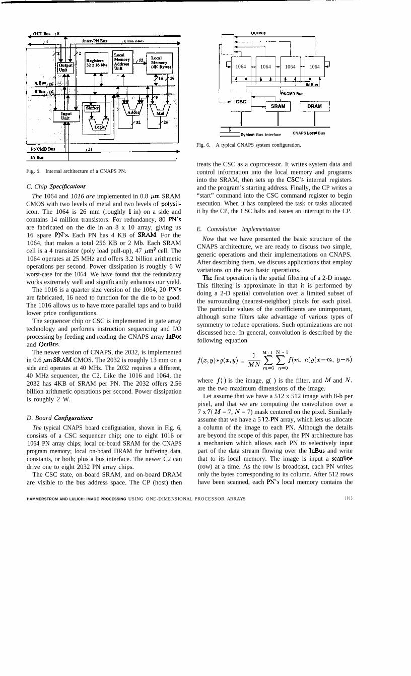
Fig. 5. Internal architecture of a CNAPS PN.
C. Chip SpecijcationsThe 1064 and 1016 are implemented in 0.8 bum SRAM
CMOS with two levels of metal and two levels of polysil-icon. The 1064 is 26 mm (roughly 1 in) on a side andcontains 14 million transistors. For redundancy, 80 PN’sare fabricated on the die in an 8 x 10 array, giving us16 spare PN’s. Each PN has 4 KB of SBAM. For the1064, that makes a total 256 KB or 2 Mb. Each SRAMcell is a 4 transistor (poly load pull-up), 47 pm* cell. The1064 operates at 25 MHz and offers 3.2 billion arithmeticoperations per second. Power dissipation is roughly 6 Wworst-case for the 1064. We have found that the redundancyworks extremely well and significantly enhances our yield.
The 1016 is a quarter size version of the 1064, 20 PN’sare fabricated, 16 need to function for the die to be good.The 1016 allows us to have more parallel taps and to buildlower price configurations.
The sequencer chip or CSC is implemented in gate arraytechnology and performs instruction sequencing and I/Oprocessing by feeding and reading the CNAPS array InBusand OutBus.
The newer version of CNAPS, the 2032, is implementedin 0.6 pm SPAM CMOS. The 2032 is roughly 13 mm on aside and operates at 40 MHz. The 2032 requires a different,40 MHz sequencer, the C2. Like the 1016 and 1064, the2032 has 4KB of SRAM per PN. The 2032 offers 2.56billion arithmetic operations per second. Power dissipationis roughly 2 W.
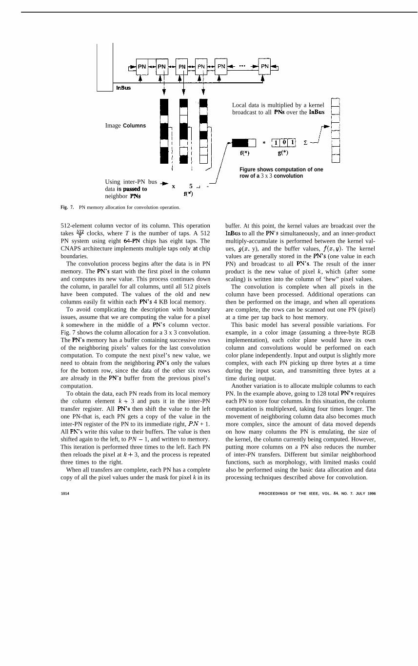
D. Board ConjigurationsThe typical CNAPS board configuration, shown in Fig. 6,
consists of a CSC sequencer chip; one to eight 1016 or1064 PN array chips; local on-board SRAM for the CNAPSprogram memory; local on-board DRAM for buffering data,constants, or both; plus a bus interface. The newer C2 candrive one to eight 2032 PN array chips.
The CSC state, on-board SRAM, and on-board DRAMare visible to the bus address space. The CP (host) then
OUTbub
c 1064 - 1064 - 1064 - 1064 3
4 c c 41
II 1 System Bus Interface CNAPS Local Bus
Fig. 6. A typical CNAPS system configuration.
HAMMERSTROM AND LULICH: IMAGE PROCESSING USING ONE-DIMENSIONAL PROCESSOR ARRAYS 1013
treats the CSC as a coprocessor. It writes system data andcontrol information into the local memory and programsinto the SRAM, then sets up the CSC’s internal registersand the program’s starting address. Finally, the CP writes a“start” command into the CSC command register to beginexecution. When it has completed the task or tasks allocatedit by the CP, the CSC halts and issues an interrupt to the CP.
E. Convolution ImplementationNow that we have presented the basic structure of the
CNAPS architecture, we are ready to discuss two simple,generic operations and their implementations on CNAPS.After describing them, we discuss applications that employvariations on the two basic operations.
The first operation is the spatial filtering of a 2-D image.This filtering is approximate in that it is performed bydoing a 2-D spatial convolution over a limited subset ofthe surrounding (nearest-neighbor) pixels for each pixel.The particular values of the coefficients are unimportant,although some filters take advantage of various types ofsymmetry to reduce operations. Such optimizations are notdiscussed here. In general, convolution is described by thefollowing equation
fb,!J)*d?Y) = j&
M - l N - l
c c f(m, n)dz-m, Y-n)m=O n=O
where f( ) is the image, g( ) is the filter, and M and N,are the two maximum dimensions of the image.
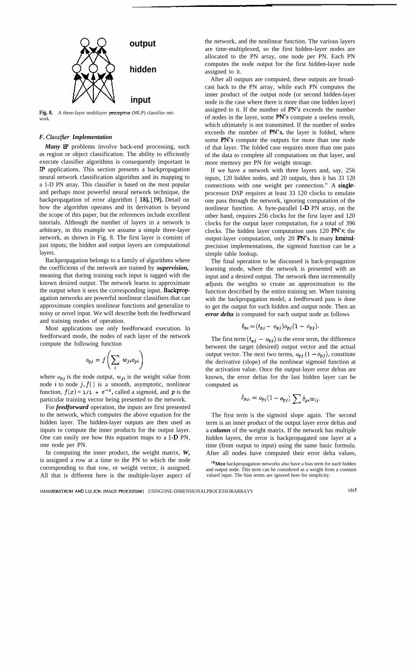
Let assume that we have a 512 x 512 image with 8-b perpixel, and that we are computing the convolution over a7 x 7( M = 7, N = 7) mask centered on the pixel. Similarlyassume that we have a 5 12-PN array, which lets us allocatea column of the image to each PN. Although the detailsare beyond the scope of this paper, the PN architecture hasa mechanism which allows each PN to selectively inputpart of the data stream flowing over the InBus and writethat to its local memory. The image is input a scanline(row) at a time. As the row is broadcast, each PN writesonly the bytes corresponding to its column. After 512 rowshave been scanned, each PN’s local memory contains the
@ PN - PN - PN
InBus
Image Columns
Using inter-PN bus -)data is passed to x 5 --I_ ,neighbor PNs I(‘)
Fig. 7. PN memory allocation for convolution operation.
512-element column vector of its column. This operationtakes y clocks, where T is the number of taps. A 512PN system using eight 64-PN chips has eight taps. TheCNAPS architecture implements multiple taps only It chipboundaries.
The convolution process begins after the data is in PNmemory. The PN’s start with the first pixel in the columnand computes its new value. This process continues downthe column, in parallel for all columns, until all 512 pixelshave been computed. The values of the old and newcolumns easily fit within each PN’s 4 KB local memory.
To avoid complicating the description with boundaryissues, assume that we are computing the value for a pixelk somewhere in the middle of a PN’s column vector.Fig. 7 shows the column allocation for a 3 x 3 convolution.The PN’s memory has a buffer containing successive rowsof the neighboring pixels’ values for the last convolutioncomputation. To compute the next pixel’s new value, weneed to obtain from the neighboring PN’s only the valuesfor the bottom row, since the data of the other six rowsare already in the PN’s buffer from the previous pixel’scomputation.
To obtain the data, each PN reads from its local memorythe column element k + 3 and puts it in the inter-PNtransfer register. All PN’s then shift the value to the leftone PN-that is, each PN gets a copy of the value in theinter-PN register of the PN to its immediate right, PN + 1.All PN’s write this value to their buffers. The value is thenshifted again to the left, to PN - 1, and written to memory.This iteration is performed three times to the left. Each PNthen reloads the pixel at k + 3, and the process is repeatedthree times to the right.
When all transfers are complete, each PN has a completecopy of all the pixel values under the mask for pixel k in its
Local data is multiplied by a kernelbroadcast to all PNs over the InBus
Figure shows computation of onerow of a 3 x 3 convolution
buffer. At this point, the kernel values are broadcast over theInBus to all the PN’s simultaneously, and an inner-productmultiply-accumulate is performed between the kernel val-ues, g(z, y), and the buffer values, f(z,v). The kernelvalues are generally stored in the PN’s (one value in eachPN) and broadcast to all PN’s. The result of the innerproduct is the new value of pixel k, which (after somescaling) is written into the column of ‘hew” pixel values.
The convolution is complete when all pixels in thecolumn have been processed. Additional operations canthen be performed on the image, and when all operationsare complete, the rows can be scanned out one PN (pixel)at a time per tap back to host memory.
This basic model has several possible variations. Forexample, in a color image (assuming a three-byte RGBimplementation), each color plane would have its owncolumn and convolutions would be performed on eachcolor plane independently. Input and output is slightly morecomplex, with each PN picking up three bytes at a timeduring the input scan, and transmitting three bytes at atime during output.
Another variation is to allocate multiple columns to eachPN. In the example above, going to 128 total PN’s requireseach PN to store four columns. In this situation, the columncomputation is multiplexed, taking four times longer. Themovement of neighboring column data also becomes muchmore complex, since the amount of data moved dependson how many columns the PN is emulating, the size ofthe kernel, the column currently being computed. However,putting more columns on a PN also reduces the numberof inter-PN transfers. Different but similar neighborhoodfunctions, such as morphology, with limited masks couldalso be performed using the basic data allocation and dataprocessing techniques described above for convolution.
1014 PROCEEDINGS OF THE IEEE, VOL. 84. NO. 7. JULY 1996
output
hidden
inputFig. 8. A three-layer multilayer perceptron (MLP) classifier net-work.
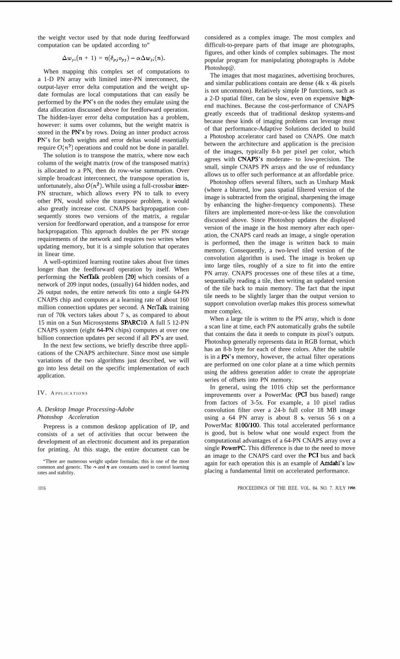
F. ClassiJer ImplementationMany Ip problems involve back-end processing, such
as region or object classification. The ability to efficientlyexecute classifier algorithms is consequently important inIP applications. This section presents a backpropagationneural network classification algorithm and its mapping toa 1-D PN array. This classifier is based on the most popularand perhaps most powerful neural network technique, thebackpropagation of error algorithm [ 181, [ 191. Detail onhow the algorithm operates and its derivation is beyondthe scope of this paper, but the references include excellenttutorials. Although the number of layers in a network isarbitrary, in this example we assume a simple three-layernetwork, as shown in Fig. 8. The first layer is consists ofjust inputs; the hidden and output layers are computationallayers.
Backpropagation belongs to a family of algorithms wherethe coefficients of the network are trained by supervision,meaning that during training each input is tagged with theknown desired output. The network learns to approximatethe output when it sees the corresponding input. Backprop-agation networks are powerful nonlinear classifiers that canapproximate complex nonlinear functions and generalize tonoisy or novel input. We will describe both the feedforwardand training modes of operation.
Most applications use only feedforward execution. Infeedforward mode, the nodes of each layer of the networkcompute the following function
/- \Opj = f LL WjiOpii )
where opj is the node output, Wj; is the weight value fromnode i to node j, f( ) is a smooth, asymptotic, nonlinearfunction, f(z) = l/l + em2, called a sigmoid, and p is theparticular training vector being presented to the network.
For feedforward operation, the inputs are first presentedto the network, which computes the above equation for thehidden layer. The hidden-layer outputs are then used asinputs to compute the inner products for the output layer.One can easily see how this equation maps to a I-D PN,one node per PN.
In computing the inner product, the weight matrix, W,is assigned a row at a time to the PN to which the nodecorresponding to that row, or weight vector, is assigned.All that is different here is the multiple-layer aspect of
the network, and the nonlinear function. The various layersare time-multiplexed, so the first hidden-layer nodes areallocated to the PN array, one node per PN. Each PNcomputes the node output for the first hidden-layer nodeassigned to it.
After all outputs are computed, these outputs are broad-cast back to the PN array, while each PN computes theinner product of the output node (or second hidden-layernode in the case where there is more than one hidden layer)assigned to it. If the number of PN’s exceeds the numberof nodes in the layer, some PN’s compute a useless result,which ultimately is not transmitted. If the number of nodesexceeds the number of PN’s, the layer is folded, wheresome PN’s compute the outputs for more than one nodeof that layer. The folded case requires more than one passof the data to complete all computations on that layer, andmore memory per PN for weight storage.
If we have a network with three layers and, say, 256inputs, 120 hidden nodes, and 20 outputs, then it has 33 120connections with one weight per connection.” A single-processor DSP requires at least 33 120 clocks to emulateone pass through the network, ignoring computation of thenonlinear function. A byte-parallel I-D PN array, on theother hand, requires 256 clocks for the first layer and 120clocks for the output layer computation, for a total of 396clocks. The hidden layer computation uses 120 PN’s; theoutput-layer computation, only 20 PN’s. In many limited-precision implementations, the sigmoid function can be asimple table lookup.
The final operation to be discussed is back-propagationlearning mode, where the network is presented with aninput and a desired output. The network then incrementallyadjusts the weights to create an approximation to thefunction described by the entire training set. When trainingwith the backpropagation model, a feedforward pass is doneto get the output for each hidden and output node. Then anerror delta is computed for each output node as follows
6pi = (tpj - Opj)Opj(l- Opj).
The first term (tpj - Opj) is the error term, the differencebetween the target (desired) output vector and the actualoutput vector. The next two terms, opj (1 - opj), constitutethe derivative (slope) of the nonlinear sigmoid function atthe activation value. Once the output-layer error deltas areknown, the error deltas for the last hidden layer can becomputed as
4% = OZJIi(l - Opj) C SpiWij.
The first term is the sigmoid slope again. The secondterm is an inner product of the output layer error deltas anda column of the weight matrix. If the network has multiplehidden layers, the error is backpropagated one layer at atime (from output to input) using the same basic formula.After all nodes have computed their error delta values,
‘OMost backpropagation networks also have a bias term for each hiddenand output node. This term can be considered as a weight from a constantvalued input. The bias terms are ignored here for simplicity.
HAMMERSTROMANDLULICH:IMAGEPROCESSING USINGONE-DIMENSIONALPROCESSORARRAYS 1015
the weight vector used by that node during feedforwardcomputation can be updated according to”
Aw+(n + 1) = q(&orj) + crAwji(n).
When mapping this complex set of computations toa 1-D PN array with limited inter-PN interconnect, theoutput-layer error delta computation and the weight up-date formulas are local computations that can easily beperformed by the PN’s on the nodes they emulate using thedata allocation discussed above for feedforward operation.The hidden-layer error delta computation has a problem,however: it sums over columns, but the weight matrix isstored in the PN’s by rows. Doing an inner product acrossPN’s for both weights and error deltas would essentiallyrequire O(n2) operations and could not be done in parallel.
The solution is to transpose the matrix, where now eachcolumn of the weight matrix (row of the transposed matrix)is allocated to a PN, then do row-wise summation. Oversimple broadcast interconnect, the transpose operation is,unfortunately, also 0(n2). While using a full-crossbar inter-PN structure, which allows every PN to talk to everyother PN, would solve the transpose problem, it wouldalso greatly increase cost. CNAPS backpropagation con-sequently stores two versions of the matrix, a regularversion for feedforward operation, and a transpose for errorbackpropagation. This approach doubles the per PN storagerequirements of the network and requires two writes whenupdating memory, but it is a simple solution that operatesin linear time.
A well-optimized learning routine takes about five timeslonger than the feedforward operation by itself. Whenperforming the NetTalk problem [20] which consists of anetwork of 209 input nodes, (usually) 64 hidden nodes, and26 output nodes, the entire network fits onto a single 64-PNCNAPS chip and computes at a learning rate of about 160million connection updates per second. A NetTalk trainingrun of 70k vectors takes about 7 s, as compared to about15 min on a Sun Microsystems SPARClO. A full 5 12-PNCNAPS system (eight 64PN chips) computes at over onebillion connection updates per second if all PN’s are used.
In the next few sections, we briefly describe three appli-cations of the CNAPS architecture. Since most use simplevariations of the two algorithms just described, we willgo into less detail on the specific implementation of eachapplication.
IV. A P P L I C A T I O N S
A. Desktop Image Processing-AdobePhotoshop Acceleration
Prepress is a common desktop application of IP, andconsists of a set of activities that occur between thedevelopment of an electronic document and its preparationfor printing. At this stage, the entire document can be
“There are numerous weight update formulas; this is one of the mostcommon and generic. The (x and 9 are constants used to control learningrates and stability.
1016
considered as a complex image. The most complex anddifficult-to-prepare parts of that image are photographs,figures, and other kinds of complex subimages. The mostpopular program for manipulating photographs is AdobePhotoshop@.
The images that most magazines, advertising brochures,and similar publications contain are dense (4k x 4k pixelsis not uncommon). Relatively simple IP functions, such asa 2-D spatial filter, can be slow, even on expensive high-end machines. Because the cost-performance of CNAPSgreatly exceeds that of traditional desktop systems-andbecause these kinds of imaging problems can leverage mostof that performance-Adaptive Solutions decided to builda Photoshop accelerator card based on CNAPS. One matchbetween the architecture and application is the precisionof the images, typically 8-b per pixel per color, whichagrees with CNAPS’s moderate- to low-precision. Thesmall, simple CNAPS PN arrays and the use of redundancyallows us to offer such performance at an affordable price.
Photoshop offers several filters, such as Unsharp Mask(where a blurred, low pass spatial filtered version of theimage is subtracted from the original, sharpening the imageby enhancing the higher-frequency components). Thesefilters are implemented more-or-less like the convolutiondiscussed above. Since Photoshop updates the displayedversion of the image in the host memory after each oper-ation, the CNAPS card reads an image, a single operationis performed, then the image is written back to mainmemory. Consequently, a two-level tiled version of theconvolution algorithm is used. The image is broken upinto large tiles, roughly of a size to fit into the entirePN array. CNAPS processes one of these tiles at a time,sequentially reading a tile, then writing an updated versionof the tile back to main memory. The fact that the inputtile needs to be slightly larger than the output version tosupport convolution overlap makes this process somewhatmore complex.
When a large tile is written to the PN array, which is donea scan line at time, each PN automatically grabs the subtilethat contains the data it needs to compute its pixel’s outputs.Photoshop generally represents data in RGB format, whichhas an 8-b byte for each of three colors. After the subtileis in a PN’s memory, however, the actual filter operationsare performed on one color plane at a time which permitsusing the address generation adder to create the appropriateseries of offsets into PN memory.
In general, using the 1016 chip set the performanceimprovements over a PowerMac (PC1 bus based) rangefrom factors of 3-5x. For example, a 10 pixel radiusconvolution filter over a 24-b full color 18 MB imageusing a 64 PN array is about 8 s, versus 56 s on aPowerMac 8100/100. This total accelerated performanceis good, but is below what one would expect from thecomputational advantages of a 64-PN CNAPS array over asingle PowerPC. This difference is due to the need to movean image to the CNAPS card over the PC1 bus and backagain for each operation this is an example of Amdabl’s lawplacing a fundamental limit on accelerated performance.
PROCEEDINGS OF THE IEEE. VOL. 84. NO. 7. JULY 19%
B. Medical Image Classification
An important area of IP and PR is processing andclassifying medical images, a field that has significantcomputing requirements and increasing pressure to decreasecosts. Reading and analyzing scanned images-whetherMRI scans, optical scans such as Pap smears, or X-raysfor suspicious structures such as cancer cells-is a matterof life or death. The process deals with noisy, ambiguousdata, and is error prone. R2 Technology in Mountain View,CA, has developed a neural network based classificationalgorithm for flagging areas of interest in mammograms.
Some of the R2 algorithm is proprietary, but we can givea simplified view of it here to show how the CNAPS 1-Darchitecture fits the problem. The X-ray images are 4K x 4Kpixels, and each pixel is a 12-b value. The basic algorithmconsists of performing two sequential convolutions of theimage using a 9 x 9 filter. The output of each filter passesthrough a nonlinear function similar to the sigmoid functionused in the back-propagation algorithm discussed above.
As with Photoshop filtering, the basic X-ray image isbroken up first into large overlapping tiles. These tiles areread into the PN array. R2 uses the 128-PN PC1 card, whichconstrains the size of the major tiles. Each major tile isthen broken into a set of 128 overlapping subtiles. Each PNoperates on its own subtile using the data in its memory. Forthe first convolution, each PN computes the values for anarray of pixels that is four units smaller (the overlap area)than the subtile. The final result of the convolution filteris then passed through the nonlinear operator (using tablelook-up). Then a smaller group of pixels (four units smalleralong the edge) are convolved using the outputs of the firstpass, and again a nonlinear operation is performed on theoutput. Finally, the output values of the last convolutionfor the major tile is output, one scanline at a time to thehost memory. Data output is overlapped with the input ofthe next tile to the PN array.
Because the algorithm employs two successive convo-lution operations, the overlap between each PN’s tile iseight, and there is some redundant computation of first-layer pixels. The tile for which PN is responsible is largeenough that the inefficiency of this overlap is minimal.
The PC1 board can scan au entire 4K x 4K X-ray forsuspicious structures in 14 s, which meets R2’s performancerequirements.
V. SUM MARY AND C ONCLUSIONS
This paper has described the Adaptive Solutions CNAPS,a 1-D SIMD processor array for IP and PR applications. Wediscussed the major architecture decisions and motivatedthese decisions. For interprocessor communication, we haveargued that for our target applications a 1-D CNAPSarray has greater cost-performance when compared to a2-D CNAPS array. We showed that if the number ofpixels is generally greater than the number of PN’s, thena I-D array can be as efficient as a 2-D array in PNutilization. We discussed internal and external I/O costissues as well as manufacturing issues such as the use of
redundant processors, indicating that a 1-D CNAPS scalesbetter and is cheaper to build. We then presented severalbrief descriptions of some real world applications of a 1-Darchitecture in image processing and recognition.
We believe that as multimedia applications and the ma-nipulation of images by computers become more wide-spread, there will be a continual need for inexpensivedesktop imaging. We also believe that architectures of thetype described here-l-D SIMD arrays with simple, low-precision fixed-point arithmetic and on-chip memory-willprovide enough performance improvement to compete fa-vorably against the fastest “super-micros” on the desktop.CNAPS, is one of the first of several chips that are startingto appear which have similar architectures. Other examplesinclude the MPACT from Toshiba and Chromatics, theMedia-Engine from MicroUnity, and the Tri-Media fromPhilips [21]. Even some of the super-micros are beginningto adopt these SIMD techniques internally, i.e., the Multi-media Extensions (MMX) to the Intel PentiumTM, the VISextensions to SparcTM, and the MAX multimedia extensionsto the HP PA 1221.
REFERENCES
[II
[21131
G. A. Baxes, Digital Image Processing-Principles and Appli-cations. New York: Wiley, 1994.Ibid, p. 21.G. D. Hutcheson and J. D. Hutcheson, ‘“Technology and eco-nomics in the semiconductor industry,” Scienrif: Amer., pp.5452, Jan. 1996.I.
[41 J. L. Hennessy and D. A. Patterson, Computer Architecture:A Quanrifative Approach. Palo Alto, CA: Morgan Kaufmann,1991.
[51
[61
[71
181
191
M. J. Quinn, Parallel Computing: Theory and Practice. NewYork: McGraw-Hill, 1994-,“The second generation image understandino.” Architec-
I101
[ill
[121
[131
ture and Beyond, pc 276285, CAMP1993. -P. Kuma, Parallel Architectures and Algorithms for ImageUnderstanding. New York: Academic, 1991.K. Preston, “Scilindustrial image processing: New systembenchmark results,” Advanced Imag., p. 46, Sept. 1992.D. Helman and J. J&U, “Efficient image processing algorithmson the scan line array processor,” IEEE Trans. Part. Anal. andMach. Intell., vol. 17, pp. 47-56, Jan. 1995.L. A. Schmitt er al., “The AIS- parallel processor,” IEEETrans. Parr. Anal. and Mach. Intell., vol. 10, pp. 320-330, May1988.N. Weste and K. Eshraghian, Principles of CMOS VLSI De-Y$~;TA System Perspective. Reading, MA: Addison-Wesley,
J. F. McDonald er al., “Yield of wafer-scale interconnections,”VLSI Sysr. Des., pp. 62-66, Dec. 1986.
I141
[I51
cl61
Cl71
V. Cantoni, C. Guerra, and S. Levialdi, “Toward an evaluationof an image processing system,” in Computing Structures forImage Processing, M. J. B. Duff, Ed. London: Academic,1983, pp. 43-56.P. P. Jonker, “Why linear arrays are better image processors,” inProc. 12th IAPR Conf: on Part. Recogn., Jerusalem, Israel, vol.3, ICPR 12; IEEE Computer Sot. Press, 1994, pp. 334-338.M. Griffin er al., “An 11 million transistor digital neural network;Tx&o; engine,” IEEE Int. Solid-Stare Circ. Co& 1991, pp.
D. Hammerstrom, W. Henry, and M. Kuhn, “The CNAPSarchitecture for neural network emulation,” in Parallel DigitalImplementations of Neural Networks, K. W. Przytula and V. K.Prasanna Kumar, Eds. Englewood Cliffs, NJ: Prentice-Hall,1993, pp. 107-138.D. Hammerstrom, “A highly parallel digital architecture forneural networks,” VLSI for Artificial Intelligence and NeuralNerworks, J. Delgado-Frias and W. Moore, Eds. New York:Plenum, 1991.
HAMMERSTROM AND LULICH: IMAGE PROCESSING USING ONE-DIMENSIONAL PROCESSOR ARRAYS 1017
[I81
[I91
PO1
Pll
WI
D. E. Rumelhart, G. E. Hinton, and R. J. Williams, “Learninginternal representations by error propagation,” in Parallel Dis-tributed Processing-Vol. I: Foundations, D. E. Rumelhart andJ. L. McClelland, Eds. Cambridge, MA: MIT Press, 1986,pp. 3 18-364.M. Smith, Neural Networks for Statistical Modeling. NewYork: Van Nostrand Reinhold, 1993.T. Sejnowski and C. Rosenberg, “NETtalk: A parallel networkthat learns to read aloud,” Tech Rep. JHUIEECS-86/01, JohnsHopkins Univ. EE and CS Dept., 1986.“DSP’s caught breaking and entering,” OEM Mug., pp. 52-58,Oct. 1995.R. B. Lee, “Accelerating multimedia with enhanced micropro-cessors,” IEEE Micro, pp. 22-32, Apr. 1995.
Daniel P. Lulich was born in 1953. He receivedthe B.S. degrees in philosophy and psychologyfrom Portland State University, Portland, OR, in1982. He also received the M.S. degree in com-puter science and engineering from the OregonGraduate Institute of Technology, Beaverton,OR.
He is presently an Applications Engineer forAdaptive Solutions Inc., Beaverton, OR. His re-search interests are image processing, computervision, neural networks, and the psychophysical
study of biological vision systems.
Dan W. Hammerstrom (Member, IEEE) wasborn in 1948. He received the B.S. degree (withdistinction) from Montana State University,Bozeman, the MS. degree from Stanford Uni-versity, Stanford, CA, and the Ph.D. degree fromthe University of Illinois, Urbana-Champaign,all in electrical engineering, in 1971, 1972, and1977, respectively.
He is presently an Associate Professor in tbeComputer Science/Engineering Department atthe Oregon Graduate Institute and is the founder
and Chief Technical Officer of Adaptive Solutions, Inc., where he workson image processing and pattern recognition applications and hardware.From 1980 to 1985 be was with Intel Corp., where he participated inthe development and implementation of the iAPX-432, the i960, and theiWarp. From 1977 to 1980, he was an Assistant Professor of ElectricalEngineering at Cornell University, Ithaca, NY, and a Computer SystemsDesign Officer in the U.S. Air Force from 1972 to 1975. He was also aVisiting Researcher at the Royal Institute of Technology in Stockholm,Sweden, in 1979 and 1984. He has been an Associate Editor for the IEEETRANSACTIONS ON NEURAL NETWORKS , the Journal of the InternationalNeural Network Sociev (INNS), and the International Journal of NeuralNetworks. He has authored over 40 research papers and seven bookchapters, and holds seven patents.
1018 PROCEEDINGS OF THE IEEE. VOL. 84, NO. 7. JULY 1996
1 I ]E -11 1 -1Fig. 4. Overview of the CNAPS architecture.
III. CNAPS A RCHITECTURE
A. Basic CNAPS ArchitectureThe CNAPS architecture consists of a I-D processor
array implemented on a custom VLSI chip. Several dif-ferent processor array chips are available: the 64ProcessorNode (PN) CNAPS-1064, the 16-PN CNAPS-1016, and inlate 1996 the 32-PN 2032. The CNAPS Sequencer Chip(CSC) governs the execution order of CNAPS instructions,broadcasts input data to the array, and reads results. The se-quencer is the external interface to the host computer, calleda control processor (CP), which interacts with the sequencerby sending it commands and writing source/destinationdata pointers. The sequencer in turn signals completion viainterrupt of the CP. CNAPS thus operates as a coprocessorto the host CP. Fig. 4 shows an overview of the CNAPSsystem.
The CNAPS architecture is a single-instruction, multiple-data (SIMD) PN array [15], [16], [17], where all PN’sexecute the same instruction every clock in synchrony. Itsinstruction word is 64-b long: 32 b specify the sequenc-ing and I/O control operations and 32 b control the PNoperations. These 64-b instructions are stored externally inSRAM, with half the memory feeding the sequencer andhalf being broadcast to all PN’s. The sequencer providesthe address to the program memory, since it controls thesequencing.
As is common with SIMD architectures, the PN’s canconditionally execute instructions based on the results ofinternal variables. Likewise, the sequencer can signal allthe PN’s to ignore an instruction, essentially causing a spinof the PN array, for example when the sequencer is waitingto read input data or to write output data.
The sequencer can drive multiple PN array chips. Thesize of the array has no architectural limit. The currentelectrical limit is eight chips-512 PN’s with the 64-PN chips, 256 PN’s with the 32-PN chips, or 128 PN’swith the 16-PN chips. Chip boundaries are invisible to theprogrammer, who is aware only of the total number of PN’sin the system. So, for example, the programmer sees nodifference between one 64 PN chip, two 32 PN chips, orfour 16 PN chips.
As can be seen in Fig. 4, the PN’s are connected into a1-D array with global broadcast from the sequencer to allPN’s (the InBus), and a global output bus (OutBus) from all
1012
PN’s to the sequencer. Each PN is connected to its nearestneighbor via a 1-D inter-PN bus. The architecture offersseveral arbitration techniques for the OutBus, the mostcommon being sequential transmission. ((PNn, PNn + 1,etc.) In addition to data transfer, the inter-PN bus is alsoused to signal the next PN during sequential arbitration. Ifmultiple PN’s transmit at once, the array performs a globalAND of all PN outputs (the default transmission is all ones).The OutBus goes into the sequencer, which can wrap thedata back around to the InBus and/or write it to memoryvia a DMA channel (StdOut). The sequencer likewise canread data from memory (StdIn) and put it on the InBus forbroadcast to the PN array.
In general, we are pleased with the architecture, but ithas several weaknesses that we plan to fix in the next gen-eration. These include the 8-b input/output, which shouldbe 16-b, since we have found that many applications needgreater I/O bandwidth. Likewise, we need more on-chipsupport for multiple taps (e.g., buffering). Within the PN’s,we found that we need a more powerful, data-driven,barrel shifter. Finally, the next generation will have asimpler, register-register RISC-like instruction set, makingit easier for the compiler to generate code. We havefound that compiling code for SIMD machines is not thatdifficult when the appropriate extensions are added to the Clanguage.’ The biggest problems in compiling C code forCNAPS are that the PN does not easily support the datatypes required by C and by the complex, microcode-likeinstruction set, leading to less efficient code generation.
B. Processor Node ArchitectureEach PN is a simple 16-b compute engine, similar to a
digital signal processor (DSP), as shown in Fig. 5. Each PNhas the following internal components, which are connectedby two 16-b internal buses:
l 9-b x 16-b multiplier;l 32-b adder;l 32 element register file (16-b);l 16-b shifter/logic operation unit;l 12-b memory address adder; andl 4096 byte memory, accessible as either 8- or 16-b
values.The instruction encoding is reasonably horizontal, SO it
allows several of the these units to operate at the same time.For example, in a typical vector inner product (“multiply-accumulate”) operation, a data element is input and sent toone half of the multiplier while the memory simultaneouslyreads the corresponding element of the multiplicand vectorand sends it to the other half of the multiplier. At the sametime, the PN computes the address for the next memorylocation to be accessed and accumulates the result of theprevious clock’s multiply with the ongoing sum. Likewise,there is hardware for quickly finding which PN has themaximum value of a particular computation.
9Adaptive Solutions has extended the C language by adoption ofthe domain structure. Domains are arrayed structures that allow theprogrammer to specify the data parallelism of the problem.
PROCEEDINGS OF THE IEEE. VOL. 84. NO. 7. JULY 1996