ilsf - 3-llrf - francis...
TRANSCRIPT

RF systems
Francis Perez

Part III:
Low
Level
RF
RF signal generatorRF signal generator
LowLow --level RF controllevel RF control
RF power distributionRF power distribution
Accelerating structureAccelerating structure
RF power AmplifierRF power Amplifier

Main Functionalities
� Control of amplitude and phase of the RF Cavity Voltage to be
synchronized with the bunch beams.
� Control of resonance frequency of the cavity (Tuning)
� RF Diagnostics
� RF interlocks
Why do we need LLRF?
� Ripples of amplifiers.
� Gain and Phase of amplifiers not linear.
� Beam loading (current of beam changes voltage of the cavity).
� Cavity drifts
LLRF

Three magnitudes have to be regulated in the RF system
Three main control loops:
• Amplitude
Precision 0.05 - 1 %
• Phase
Precision 0.01 - 0.5 °
• FrequencyPrecision 1 - 100 Hz
LLRF main loops

RF Drive
Plunger
Cav
Volt
IOT
Pre
Amp
Analog Front End
SR LLRF
Analog Front End
RF ( 500 MHz )
IF ( 20 . MHz )
IF ( 20 . MHz )
RF Control
Beam
General concept:
- Measure the relevant
parameter
- Compare with reference
- Use the difference and PI
control to define the action.
- Act in the amplifier chain
LLRF control loops

LLRF amplitude/phase loop
- Pick up a sample of the voltage inside the
cavity, get amplitude and phase.
- Compute the error (difference measured
respect the setting)
- Use the error signal to drive the amplifier
chainPickup loop

LLRF tuning loop
- A way to measure the mismatch of cavity with amplifier
- Compute the error (difference measured respect the setting)
- Use the error signal to drive the tuner motor

RF Drive
Beam
Plunger Plunger
Cav
Volt
Cell 2
Volt
Cell 4
Volt
Booster LLRF
IOT
Cav Fw
Pre
Amp
Other loops
Field flatness loop in a multicell cavity.Maintain the voltage along the cells constant
Act on plunger in cells 2 and 4.
ALBA

The idea is to pickup a sample of the voltage in the cavity and, after
proper amplification, combine it, 180° dephased, with the driving
signal of the amplitude loop.
CavityPickup
PowerCouplerAmplitude
Loop
RF Drive Combiner VariableAttenuator
VariableAttenuator
180Phase shifter
o
Amplifier
Amplifier Gain K
Directive Coupler
Other loops
Fast RF feedback for beam loading compensation
ANKA
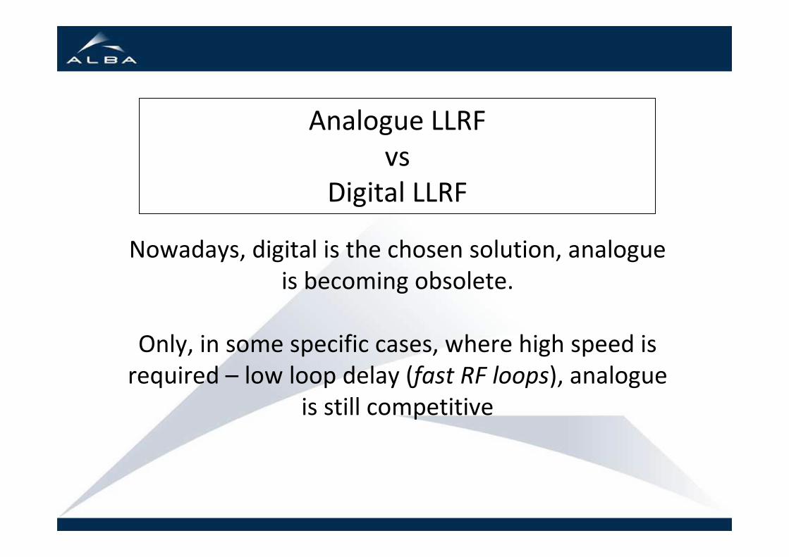
Analogue LLRF
vs
Digital LLRF
Nowadays, digital is the chosen solution, analogue
is becoming obsolete.
Only, in some specific cases, where high speed is
required – low loop delay (fast RF loops), analogue
is still competitive

» Higher precision, lower noise
amplitude down to 0.01% and phase 0.01 degrees
» Flexible, modifications in “software”
by reprogramming the FPGA
» Allows the parameterization of the loopsfor example, change the loop gains on the flight
» Allows better diagnostics
one can check how the loop is working with inside FPGA diagnostics
» Nowadays, can even be cheaper than analogue
Advantages of the digital system

As an example
the
ALBA Digital LLRF system
by Angela Salom
Analog Front End
Down Conversion
FPGA
Digital IQ Demodulation
8DACs80MHz
Analog Front End
UpConversion
IOT2
RF Cavity Voltage (500MHz)
IF
RF Forward Cavity Voltage(500MHz)
Analog Timing System520MHz 500MHz
80MHz 80MHz
CAVITY
Tuning Control Loop
Digital Timing SystemPCI Bus
ICEPAPMotor Controller
13 RF Diagnostic Signals (500MHz)
IQ Ctrl IOT1& IOT2
IOT1CACO
DC
500MHz
8 ADCs80MHz
8 ADCs80MHz
FPGA
Digital IQ Demodulation and Control Loops
Digital Timing System
Analog Front End
Down Conversion
FPGA
Digital IQ Demodulation
8DACs80MHz
Analog Front End
UpConversion
IOT2
RF Cavity Voltage (500MHz)
IF
RF Forward Cavity Voltage(500MHz)
Analog Timing System520MHz 500MHz
80MHz 80MHz
CAVITY
Tuning Control Loop
cPCI Bus
ICEPAPMotor Controller
13 RF Diagnostic Signals (500MHz)
IQ Ctrl IOT1& IOT2
IOT1CACO
DC
500MHz
8 ADCs80MHz
8 ADCs80MHz
FPGA
Digital IQ Demodulation and Control Loops
Commercial Digital Board: cPCI
Analog Front End
Down Conversion
FPGA
Digital IQ Demodulation
8DACs80MHz
Analog Front End
UpConversion
IOT2
RF Cavity Voltage (500MHz)
IF
RF Forward Cavity Voltage(500MHz)
Analog Timing System520MHz 500MHz
80MHz 80MHz
CAVITY
Tuning Control Loop
Digital Timing SystemPCI Bus
ICEPAPMotor Controller
13 RF Diagnostic Signals (500MHz)
IQ Ctrl IOT1& IOT2
IOT1CACO
DC
500MHz
8 ADCs80MHz
8 ADCs80MHz
FPGA
Digital IQ Demodulation and Control Loops
Analog Front End
Down Conversion
FPGA
Digital IQ Demodulation
8DACs80MHz
Analog Front End
UpConversion
IOT2
RF Cavity Voltage (500MHz)
IF
RF Forward Cavity Voltage(500MHz)
Analog Timing System520MHz 500MHz
80MHz 80MHz
CAVITY
Tuning Control Loop
Digital Timing SystemPCI Bus
ICEPAPMotor Controller
13 RF Diagnostic Signals (500MHz)
IQ Ctrl IOT1& IOT2
IOT1CACO
DC
500MHz
8 ADCs80MHz
8 ADCs80MHz
FPGA
Digital IQ Demodulation and Control Loops
Control Inputs
Diagnostics Inputs
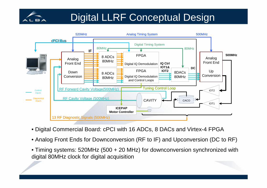
Digital LLRF Conceptual Design
• Digital Commercial Board: cPCI with 16 ADCs, 8 DACs and Virtex-4 FPGA
• Analog Front Ends for Downconversion (RF to IF) and Upconversion (DC to RF)
• Timing systems: 520MHz (500 + 20 MHz) for downconversion synchronized with digital 80MHz clock for digital acquisition
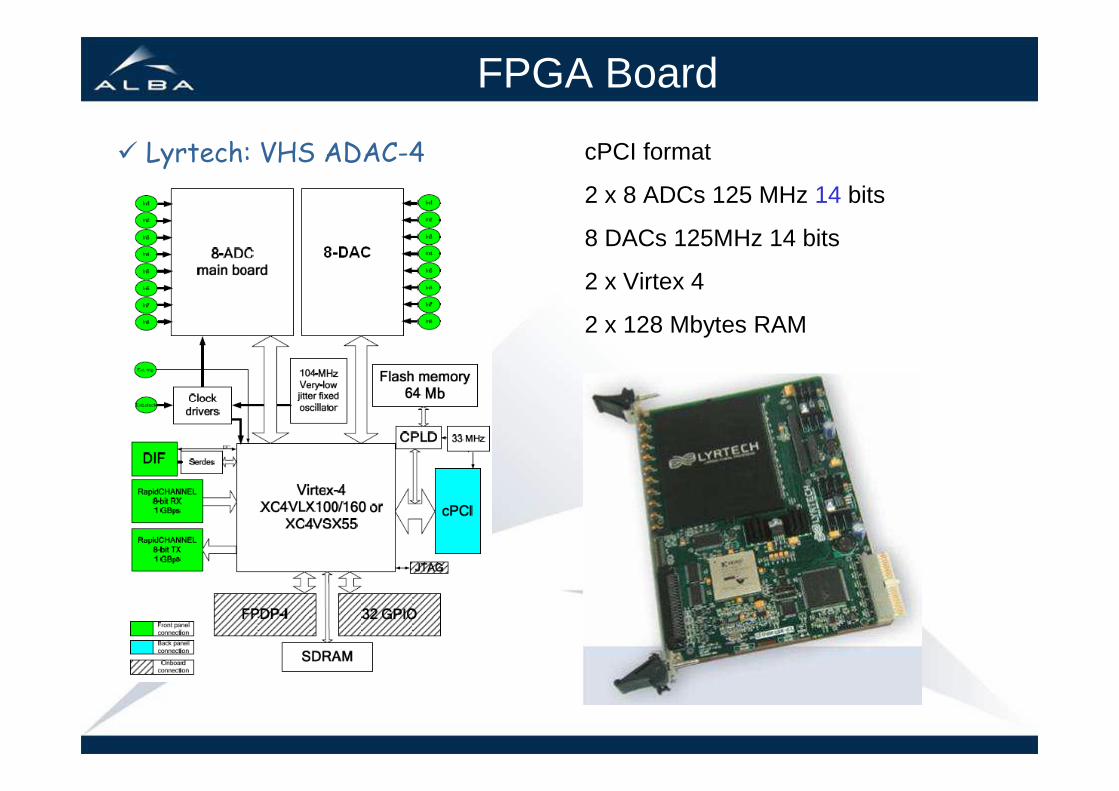
FPGA Board
� Lyrtech: VHS ADAC-4 cPCI format
2 x 8 ADCs 125 MHz 14 bits
8 DACs 125MHz 14 bits
2 x Virtex 4
2 x 128 Mbytes RAM

IQ Demodulation� Demodulation
Removal of the periodic variation of a signal keeping its information, i.e. transform a waveform signal into baseband or DC.
�IQ Demodulation
Comparison between two signals to obtain the quadrature and in phase components of the signal demodulated in comparison to the reference signal
Reference: Master Oscillator Clock (500MHz)
Cavity Voltage: 500MHz
I: In Phase Component (0°)
Q: In Quadrature component (90°)
Amp:
Φ:
22 QI +
)tan(IQ
a
R F C avity Vo ltage
M aster O sc illator
I Q
IQ
I Q
IQ
φ
Amp
I
Q
Master Oscillator
φ
�Phasor Diagram: I&Q
RF Systems of ALBA, March 13th, 2013 15/67

Freq ( MHz )20 1020
cos ( ß ) · cos (α ) = ½ · ( cos (α - ß ) + cos ( α + ß ))
+
Freq ( MHz )500 520
cos ( ß ) · cos (α )
Downconversion: From RF to IF
Ref Signal (520 MHz) = MO + IF
ADCs Clock = 4*IF
Phase shifter to adjust phase
delay lines between RF plants

Upconversion: From DC to RF
IQ Modulator
DC I Control
DC Q Control
MO (500MHz)
RF Drive
The MO signal is modulated, by I & Q,
in amplitude and phase

Timing System
VCXO (160MHz)
1/2
1/8
0/90º
IQ Mod
520MHz for Downconversion
Bandpass filter
Digital Timing System Analog Timing System
20MHz
80MHzCLK
10MHz
MO (500MHz)
Needed for proper digitalization and synchronization

Control Loops

Amplitude and Phase Control Loops� Digital IQ Demodulation
� PI Control Loop for IQ
Accumulator
+
-
+
+
+
+
P action
Integral
action
Set Point Kp
Input
(I,Q)Control
Signal
Ki
error
Settings
Diagnostics
IQ
-I
-Q
IQ
20 MHz
I
Q
I
QIF 20 MHz
Dem
uxADC80MHz
80MHz Clk
80MHz Clk
1 2 3 4 1 2 3 ... SW Reference Counter
ActionIntegral ActionalProportion
k Error
k Error
kError
InputSetPoint
operator) theby set be (to
achieve to VoltageCav
voltageCavity of Components IQ
i
ti
P
+⋅
⋅⋅
−
∑
Inputs:
Set Point:
Error:
P Action:
I Action:
Accum Error:
Control Signal:

Amplitude and Phase Control LoopsDifferent PI Loop responses: Over-damp
Cavity Gain: 0.25; Kp gain = 1; Ki gain = 1
tInput Ref
error
Error accum e * kp
e accum * ki
Control action
0 0.0 0.0 0.0 0.0 0.0 0.0 0.0
1 0.0 100 100 100 100 100 200
2 50 100 50 150 50 150 200
3 50 100 50 200 50 200 250
4 62.5 100 37.5 237.5 37.5 237.5 275
… … … … … … … …
30 99.8 100.0 0.2 399.3 0.2 399.3 399.5
Accumulator
+
-
+
+
+
+
P action
Integral action
Set Point Kp
Input
Control Signal
Ki
error
Cavity
Input = Control Signal * Cavity Transfer Function
Cavity Gain 0.25; Ki 1; Kp 1
0.0
50.0
100.0
150.0
200.0
250.0
300.0
350.0
400.0
450.0
0 5 10 15 20 25 30 35
Input Reference control

Amplitude and Phase Control LoopsDifferent PI Loop responses: Under-damp
Cavity Gain: 0.25; Kp gain = 2; Ki gain = 3
t Input Ref errorError accum e * kp
e accum * ki
Control action
0 0.0 0 0 0 0 0 0
1 0.0 100 100 100 200 300 500
2 125 100 -25 75 -50 225 175
3 43.8 100 56.3 131.3 112.5 393.8 506.3
4 126.6 100 -26.6 104.7 -53.1 314.1 260.9
… … … … … … … …
30 100.4 100 -0.4 133.1 -0.8 399.4 398.6
Accumulator
+
-
+
+
+
+
P action
Integral action
Set Point Kp
Input
Control Signal
Ki
error
Cavity
Input = Control Signal * Cavity Transfer Function
Cavity Gain 0.25; kp 2; ki 3
0.0
100.0
200.0
300.0
400.0
500.0
600.0
0 5 10 15 20 25 30 35
input reference Control action

Characterization of Cavity Transfer Function
Transfer Function: Mathematical representation of a system (model)� to be calculated analytically
� to be measured experimentally
Experimentally: Step response in Open Loop
Cav Volt
Reference
� Group Delay = 1.93µs� ζ (63%) = 9.7 µs� Gain = 0.8� Filling time = 29.3 µs
Transfer Function
s.
e.s
eK sTs
6
102
10791
80
1
6
−
⋅⋅−−
⋅+⋅=
τ+⋅
−
System Characterization (1st Order)
(DAMPY Cavity)

Amplitude and Phase Control Loop
Step response in Close Loop (Cav&DACs)
0.95 1 1.05 1.1 1.15
x 10-3
30
40
50
60
70
80
90
100
t(s)
Cav
Sig
nals
(m
V)
ICavQCavCavAmpIRefCavRef
0.95 1 1.05 1.1 1.15 1.2
x 10-3
20
40
60
80
100
120
140
160
t(s)
DA
Cs
Out
put
(mV
)
IDACQDAC
Diagnostics signals of Loops
IQ Cav IQ FwCav Amplitude Fw AmplitudeCav Phase Fw Phase
IQ Error Control AmplitudeIQ Integral Action Control PhaseIQ PID Output
fRF
freq
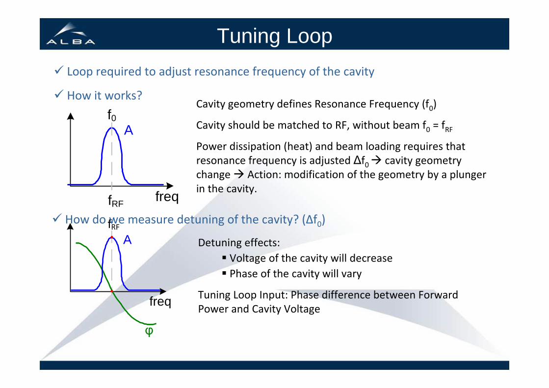
Tuning Loop
� Loop required to adjust resonance frequency of the cavity
� How it works?
� How do we measure detuning of the cavity? (Δf0)
Cavity geometry defines Resonance Frequency (f0)
Cavity should be matched to RF, without beam f0 = fRF
Power dissipation (heat) and beam loading requires that
resonance frequency is adjusted ∆f0 � cavity geometry
change � Action: modification of the geometry by a plunger
in the cavity.
Af0
freqfRF
Detuning effects:
� Voltage of the cavity will decrease
� Phase of the cavity will vary
Tuning Loop Input: Phase difference between Forward
Power and Cavity Voltage
φ
A

Tuning Loop� Cordic Algorithm to calculate Cav – Fw phase difference
Iterative process to calculate phase without employing any multipliersResolution better than 0.001º after 16 iterations (1/80MHz * 16 = 0.2 µs)
� Tuning Loop not always active to avoid plunger oscillations around 0ºphase
t=t0 ∆φ < -3º Tuning Ont=t1 ∆φ = 1º Tuning Offt=t2 ∆φ < -3º Tuning Ont=t3 ∆φ = 1º Tuning Off
� Tuning Outputs: Two LVTTL signals (Pulse and direction)
Motor Driver Control : IcepapFrequency of the pulses adjustable (from 100Hz to 2kHz)
Results on real cavity @ 20kW
t0 t1 t2 t3-3
-101
3
Fw&Cav Dephase
Cavity Reflected Power
t(s)
Pha
se (
º)
Pow
er (
a.u.
)

High Power testUp to 80 kW
y = 0.0004x2 - 0.0007x
R2 = 1
0
10
20
30
40
50
60
70
80
90
0 50 100 150 200 250 300 350 400 450 500
IQ Drive [mV]
Pow
er [k
W]
Power Tests
Power tests at ALBA High Power RF Lab from 80W to 80kW
0 50 100 150 200 250
0
10
20
30
40
50
60
70
80
90
100
t(s)
mV
- D
egre
es
Reflected Cav
Cav Volt
Fw Cav Volt
Amp & Ph loop OFFAmp & Ph loop ON -
Slow PID
Amp & Ph loop ON -Fast PID
Dynamic range: 30 dB
Loops performance:
Amplitude, Phase and Tuning loops simultaneously in
operation
Close Loop
Open Loop

Booster Ramping� Ramping to accelerate from 100MeV to 3GeV
100MeV
3GeV
333ms
BTS extraction
LTB Injection
333ms
3Hz TRG
t1 t2 t3 t4 t1 t2 t3 t4
Cav Volt Init
Cav Volt End
Tuning Pulses
Ramping Timing
� Parameters to be set by LLRFTiming
t1: Time to start ramp up after trigger
t2: Ramp up timet3:Top ramping time
t4: Ramping down time
Cavity Voltage
Cavity voltage at Ramping startCavity Voltage at Top Ramp
� Amplitude and Phase loops always active
�Tuning Loop only active at Top of the ramp

Booster Field Flatness (FF)� Booster Cavity: 5 cells
� Field Flatness loop: to keep the same voltage at 5 cells
� How does it work?
RF Drive
Beam
Plunger Plunger
Cav Volt
Cell2 Volt
Cell4 Volt
Booster LLRF
IOT
Cav Fw
Pre Amp
Cell 3: Input of Amplitude and Phase loop (Cavity Voltage)
Cell 2 and Cell 4: Inputs of Field Flatness loop
Actuator: Two Plungers
φ (CavFw) ∆A (Cell2-Cell4) Tuning FF PLG1 PLG2
φ > TM -- ON OFF ↑ ↑
φ < -TM -- ON OFF ↓ ↓
-TM < φ < TM ∆A > FFM OFF ON ↑ ↓
-TM < φ < TM ∆A < -FFM OFF ON ↓ ↑
-TM < φ < TM -FFM < ∆A < FFM OFF OFF Stop Stop
TM: Tuning Margin FFM: FF Margin
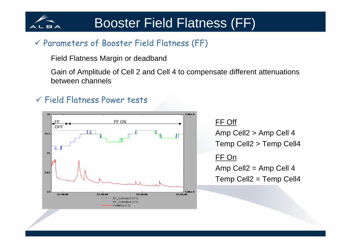
Booster Field Flatness (FF)� Parameters of Booster Field Flatness (FF)
Field Flatness Margin or deadband
Gain of Amplitude of Cell 2 and Cell 4 to compensate different attenuations between channels
� Field Flatness Power tests
FF ONFF OFF
FF OffAmp Cell2 > Amp Cell 4
Temp Cell2 > Temp Cell4
FF On
Amp Cell2 = Amp Cell 4Temp Cell2 = Temp Cell4
RF Diagnostics

RF Diagnostics
�CavityCavity PowerForward and Reversed Cavity Power
� Waveguide SystemFw and Rv Circulator InputFw and Rv Circulator OutputFw and RV Load Power
�Transmitter SignalsFw Transmitter1 Input PowerFw Transmitter2 Input PowerFw and Rv IOT-01 PowerFw and Rv IOT-02 Power
Other RF signals Digital IQ Demodulated
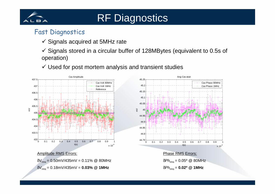
RF DiagnosticsFast Diagnostics
� Signals acquired at 5MHz rate
� Signals stored in a circular buffer of 128MBytes (equivalent to 0.5s of operation)
� Used for post mortem analysis and transient studies
Booster Ramping @ 3Hz
0 0.1 0.2 0.3 0.4 0.5 0.6 0.7 0.8 0.9 1
x 10-4
433
433.5
434
434.5
435
435.5
436
436.5
437
437.5Cav Amplitude
t(s)
mV
Cav Volt 80MHz
Cav Volt 1MHzReference
Amplitude RMS Errors:
δVrms = 0.50mV/435mV = 0.11% @ 80MHz
δVrms = 0.18mV/435mV = 0.03% @ 1MHz
0 0.1 0.2 0.3 0.4 0.5 0.6 0.7 0.8 0.9 1
x 10-4
44.75
44.8
44.85
44.9
44.95
45
45.05
45.1
45.15
45.2
45.25Ang Cav atan
t(s)
mV
Cav Phase 80MHz
Cav Phase 1MHz
Phase RMS Errors:
δPhrms = 0.05º @ 80MHz
δPhrms = 0.02º @ 1MHz

RF Diagnostics
0 0.5 1 1.5 2 2.5 3 3.5 4
x 10-3
100
110
120
130
140
150Beam Phase
t(s)
(º)
Beam Phase (º)
0 0.5 1 1.5 2 2.5 3 3.5 4
x 10-3
0
2
4
6
8
10
12Cav Dis - RvCav - Beam Power
t(s)
kW
Cav DisBeamPowerRvCav
Behavior of 06B after a trip in 10B and no beam dump (61mA)
Post Mortem Analysis Example
�Power to beam increases
�Beam phsae gets reduced
�Frequency oscillations ~ 6kHz (synchrotron freq)
�Stabilization time ~ 3ms (longitudinal damping time)
RF Diagnostics
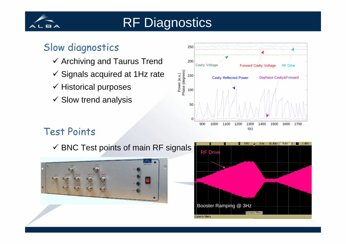
Slow diagnostics� Archiving and Taurus Trend
� Signals acquired at 1Hz rate
� Historical purposes
� Slow trend analysis
Test Points
� BNC Test points of main RF signals
900 1000 1100 1200 1300 1400 1500 1600 1700
0
50
100
150
200
250
t(s)
Pow
er (
a.u.
)P
hase
(de
gree
s)
Dephase Cavity&ForwardCavity Reflected Power
Cavtiy Voltage Forward Cavtiy Voltage RF Drive
Booster Ramping @ 3Hz
RF Drive
Conditioning
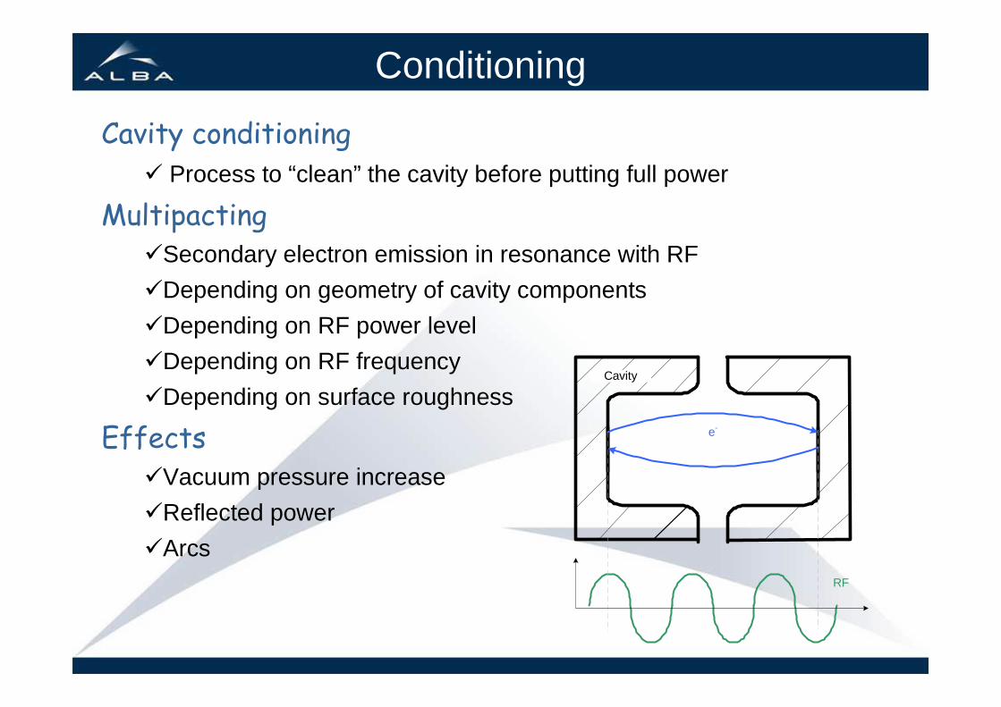
Conditioning
Cavity conditioning� Process to “clean” the cavity before putting full power
Multipacting�Secondary electron emission in resonance with RF
�Depending on geometry of cavity components
�Depending on RF power level
�Depending on RF frequency
�Depending on surface roughness
Effects�Vacuum pressure increase
�Reflected power
�Arcs
e-
RF
Cavity

Manual ConditioningRF Drive square modulated
�Duty Cycle of pulses adjustable (1-100%)
�Amplitude adjustable
�Time between pulses = 100ms (10Hz)
� Tuning Loop only enable at top of the pulses
Drawbacks
�Operator needed to adjust amplitude and duty cycle
�Vacuum levels not considered by LLRF �frequent interlocks

Automated Conditioning
�Amplitude and duty cycle increase depending on vacuum levels
�Amplitude increase rate (slope): adjusted by operator
�Vacuum signal connected to LLRF
� Vacuum < Limit Down � Voltage Amplitude Increases/Decreases
� Vacuum > Limit Up � Voltage Amplitude remains constant until vacuum is below limit down
Voltage Increase rate set to 0.03mV/s Voltage Decrease rate set to 1mV/s
8kW
1kW
600W
Pow
er (
kW)
Power Down
0 50 100 1500
2
4
6x 10
-7
Vac
uum
(m
bar)
Vacuum
Cavity Reference
Cavity Voltage0
2
5
x 10-7 Power Up
Vac
(m
bar)
0 50 100 150 200 250 300 35045
50
55
60
65
Pow
er (
a.u.
)
Cavity Reference
Cavity Voltage
Vacuum
Vac Limit Up
Vac Limit Down

Automatic Startup

RF Power
Tuning pulses
Plungers direction
After an RF trip, LLRF goes to Standby State:�Low RF Drive�Tuning Disable�Amplitude and Phase loops opened
After resetting the interlock and switching on transmitter� Detection of RF presence in cavity� Cavity tuning before increasing power� Amplitude and Phase Loops closed at low power� Smooth power increase� Message: Ready for beam operation
Automatic Startup without beam

RF Plant GUI

RF Plant GUI
Transmitters Information Cavity Interlocks from EPS
Fast Interlocks
(FIM)
EPS Interlocks of RF Auxiliaries
LLRF Settings
Operation Modes

Thank you
Francis Perez