ihp bicmos technologies for rf and mixed signal...
TRANSCRIPT
IHPIm Technologiepark 2515236 Frankfurt (Oder)
Germany
IHP Im Technologiepark 25 15236 Frankfurt (Oder) Germany www.ihp-microelectronics.com © 2011 - All rights reserved
IHP BiCMOS technologies for RF and mixed signal applications
August 26 - 28, 2012
R.F. Scholz, F. Teply, M. Cirillo
Fourth International Workshop onAnalogue and Mixed Signal Integrated Circuits
for Space Applications
IHP Im Technologiepark 25 15236 Frankfurt (Oder) Germany www.ihp-microelectronics.com © 2012 - All rights reserved
Introduction
0.25µm BiCMOS – SGB25V/SGB25RH
- Technology description
- Evaluation Status
- Running radhard library project
- Other projects using SGB25V technology
0.13µm BiCMOS - SG13S
Outline

IHP Im Technologiepark 25 15236 Frankfurt (Oder) Germany www.ihp-microelectronics.com © 2012 - All rights reserved
IHP in a Nutshell● Institute of the Leibniz Association Owned by the State of Brandenburg; limited liability
company since 1991
● Founded in 1983 Long term experience in silicon technology & materials research
● Silicon based high-frequency technologies, circuits and systems
for the wireless and broadband communication
● 300 people from 20 countriesAmong them 139 scientists
● Certified DIN EN ISO 9001:2008
IHP Im Technologiepark 25 15236 Frankfurt (Oder) Germany www.ihp-microelectronics.com © 2012 - All rights reserved
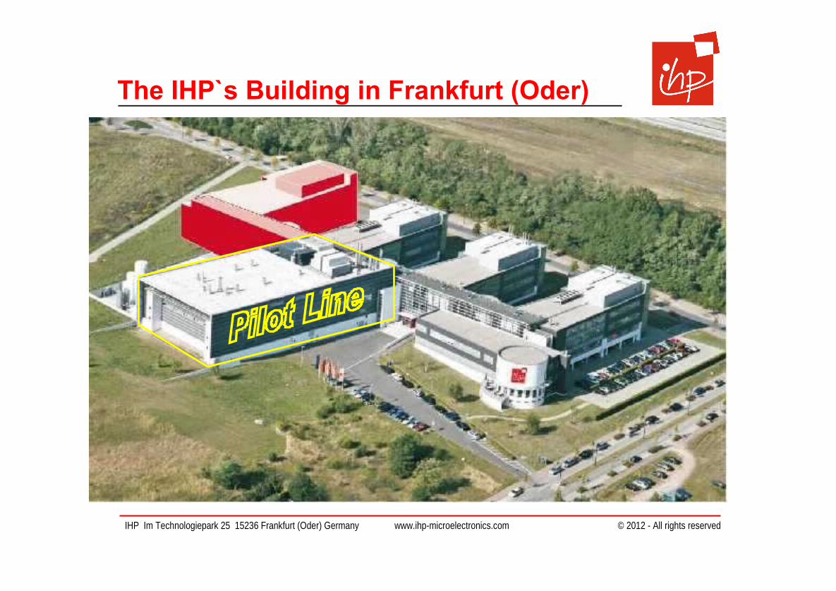
The IHP`s Building in Frankfurt (Oder)
IHP Im Technologiepark 25 15236 Frankfurt (Oder) Germany www.ihp-microelectronics.com © 2012 - All rights reserved
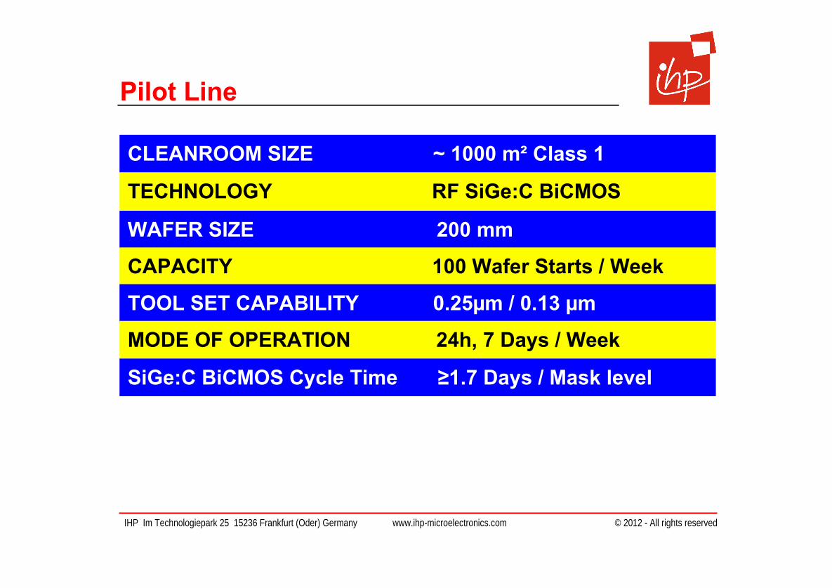
Pilot Line
Summer 2001
TECHNOLOGY RF SiGe:C BiCMOS
CLEANROOM SIZE ~ 1000 m² Class 1
WAFER SIZE 200 mm
CAPACITY 100 Wafer Starts / Week
TOOL SET CAPABILITY 0.25µm / 0.13 µm
MODE OF OPERATION 24h, 7 Days / Week
SiGe:C BiCMOS Cycle Time ≥1.7 Days / Mask level
IHP Im Technologiepark 25 15236 Frankfurt (Oder) Germany www.ihp-microelectronics.com © 2012 - All rights reserved
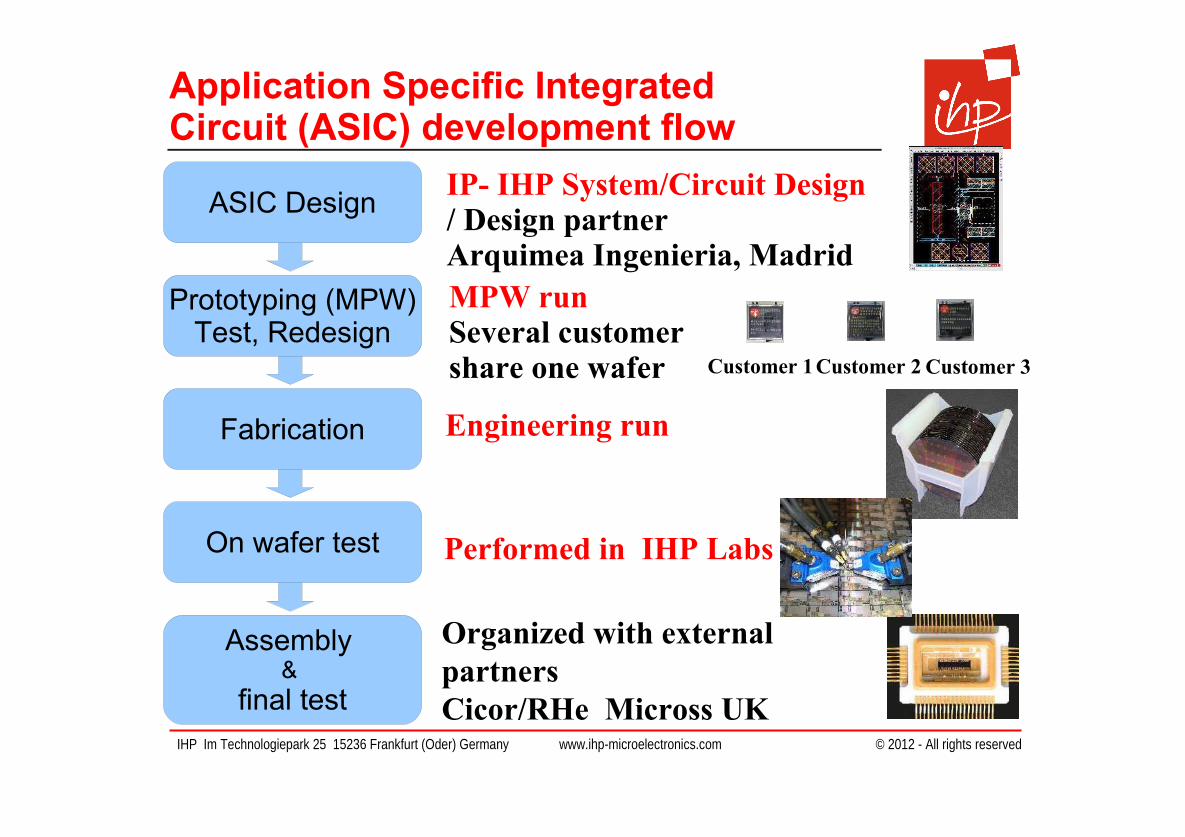
IP- IHP System/Circuit Design / Design partner Arquimea Ingenieria, Madrid
Application Specific Integrated Circuit (ASIC) development flow
MPW runSeveral customer share one wafer Customer 2Customer 1 Customer 3
ASIC Design
Fabrication
Assembly &
final test
On wafer test
Prototyping (MPW)Test, Redesign
Organized with external partnersCicor/RHe Micross UK
Engineering run
Performed in IHP Labs
IHP Im Technologiepark 25 15236 Frankfurt (Oder) Germany www.ihp-microelectronics.com © 2012 - All rights reserved
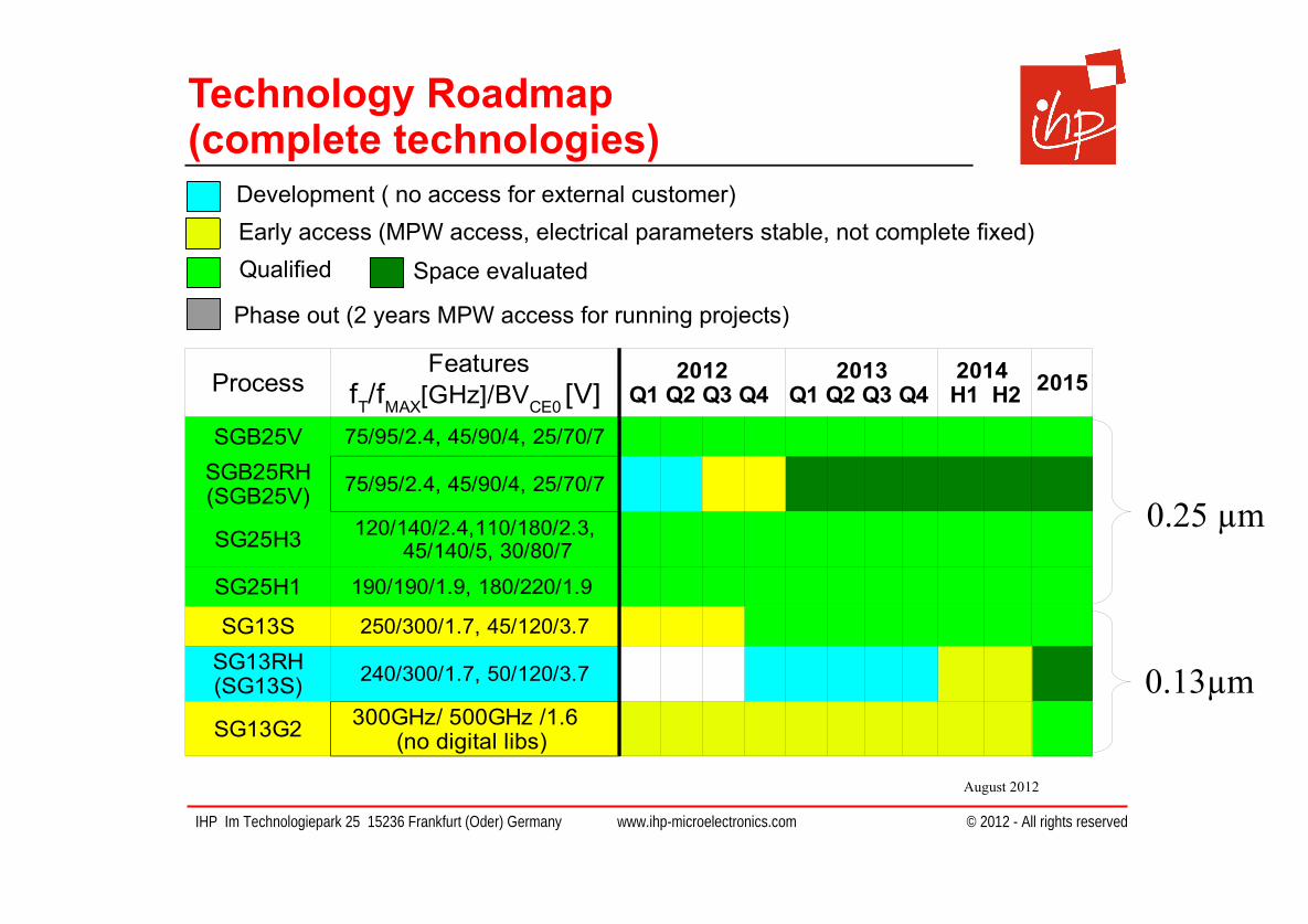
Technology Roadmap (complete technologies)
Development ( no access for external customer)
Early access (MPW access, electrical parameters stable, not complete fixed)
Qualified
Phase out (2 years MPW access for running projects)
Space evaluated
August 2012
2015
SGB25V 75/95/2.4, 45/90/4, 25/70/7
75/95/2.4, 45/90/4, 25/70/7
SG25H3
SG25H1
SG13S 250/300/1.7, 45/120/3.7
240/300/1.7, 50/120/3.7
SG13G2
Process Features
fT/f
MAX[GHz]/BV
CE0 [V]
2012 Q1 Q2 Q3 Q4
2013 Q1 Q2 Q3 Q4
2014 H1 H2
SGB25RH (SGB25V)
120/140/2.4,110/180/2.3, 45/140/5, 30/80/7
190/190/1.9, 180/220/1.9
SG13RH (SG13S)
300GHz/ 500GHz /1.6 (no digital libs)
0.25 µm
0.13µm
IHP Im Technologiepark 25 15236 Frankfurt (Oder) Germany www.ihp-microelectronics.com © 2012 - All rights reserved
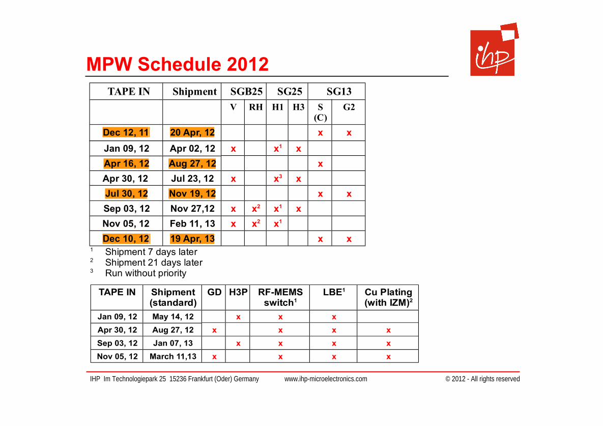
MPW Schedule 2012TAPE IN Shipment SGB25 SG25 SG13
V RH H1 H3 S(C)
G2
Dec 12, 11 20 Apr, 12 x x
Jan 09, 12 Apr 02, 12 x x1 x
Apr 16, 12 Aug 27, 12 x
Apr 30, 12 Jul 23, 12 x x3 x
Jul 30, 12 Nov 19, 12 x x
Sep 03, 12 Nov 27,12 x x2 x1 x
Nov 05, 12 Feb 11, 13 x x2 x1
Dec 10, 12 19 Apr, 13 x x1 Shipment 7 days later2 Shipment 21 days later3 Run without priority
TAPE IN Shipment(standard)
GD H3P RF-MEMSswitch1
LBE1 Cu Plating(with IZM)2
Jan 09, 12 May 14, 12 x x x
Apr 30, 12 Aug 27, 12 x x x x
Sep 03, 12 Jan 07, 13 x x x x
Nov 05, 12 March 11,13 x x x x
IHP Im Technologiepark 25 15236 Frankfurt (Oder) Germany www.ihp-microelectronics.com © 2012 - All rights reserved
Introduction
0.25µm BiCMOS – SGB25V/SGB25RH
- Technology description
- Evaluation Status
- Running radhard library project
- Other projects using SGB25V technology
0.13µm BiCMOS - SG13S
Outline

IHP Im Technologiepark 25 15236 Frankfurt (Oder) Germany www.ihp-microelectronics.com © 2012 - All rights reserved
SGB25RH Process Options
Features SGB25V / SGB25RH Full BiCMOS
CMOS Vdd=2.5V, Tox=5nm
CMOS logic Digital libraries
Passives
Interconnects 5 layer Al incl. 2µm & 3µm thick layers
Bipolar (fT/fmax/BVCE0)
High-speed HBT: 80 GHz/ 100 GHz/ 2.4 V Medium-voltage HBT: 45 Ghz/ 120 GHz /4 V High-voltage HBT: 28 GHz/ 120 GHz/ 7 V
Poly-Si resistors, MIM capacitors, MOS varactors, a.o.
IHP Im Technologiepark 25 15236 Frankfurt (Oder) Germany www.ihp-microelectronics.com © 2012 - All rights reserved
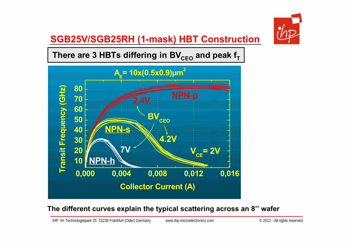
SGB25V/SGB25RH (1-mask) HBT Construction
The different curves explain the typical scattering across an 8’’ wafer
There are 3 HBTs differing in BVCEO and peak fT
0,000 0,004 0,008 0,012 0,016
1020304050607080
NPN-h7V
4.2VNPN-s
2.4V
BVCEO
NPN-p
AE= 10x(0.5x0.9)µm2
VCE
= 2V
Tra
nsi
t F
req
uen
cy (
GH
z)
Collector Current (A)

IHP Im Technologiepark 25 15236 Frankfurt (Oder) Germany www.ihp-microelectronics.com © 2012 - All rights reserved
SGB25RH Elements and Applications
Basic structure elements:
PMOS NMOSI solated NMOS MOS Varactor RPND resistor RSIL resistor RPPD resistor RHIGH resistor MIM Capacitor npnVS bipolar HBT npnVH bipolar HBT npnVP bipolar HBT Inductor made by backend metal layer Antenna diode ESD clamp Digital standard cells Digital IO cells
Components in CMOS, bipolarand BiCMOS
Maximal application frequency up to 20 GHz as chip or packaged Mixed Signal Technology fast counters fast shift register FlipFlops Dividers Frequency-/Phase comparator Charge pumps VCOs Linear amplifiers Current sources PLLs (integer and fractional) Digital Analog Converters etc.

IHP Im Technologiepark 25 15236 Frankfurt (Oder) Germany www.ihp-microelectronics.com © 2012 - All rights reserved
Schematic entry
Virtuoso
IHP Cadence DFII Design Flow
layout input
Virtuoso
LVS
Assura
EM simulation
MOMENTUM SONNET
Waveform Viewer
AWD, DDSGDSII
xstream
Layout design SimulationSchematic entry
Parasitic Extraction
Assura/QRCCOLUMBUS
Filler Generation
Assura
DRC
Assura
Mixed signal & RF simulation
APS (AMS Designer)Spectre/GoldenGate
Tape-out
Digital entry
Encounter
IHP Im Technologiepark 25 15236 Frankfurt (Oder) Germany www.ihp-microelectronics.com © 2012 - All rights reserved
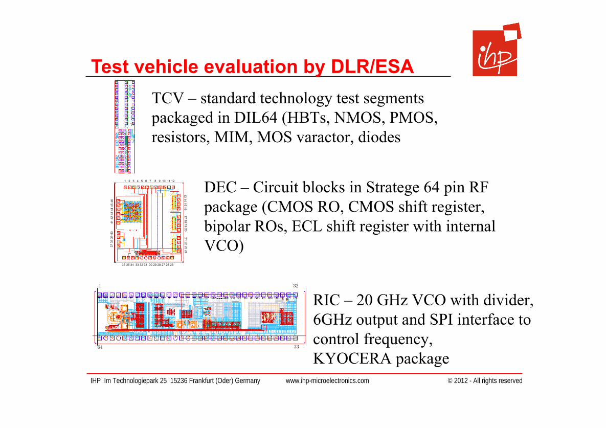
Test vehicle evaluation by DLR/ESA
1 2 3 4 5 6 7 8 9 10 11 12
36 35 34 33 32 31 30 29 28 27 26 25
13 1 4 1 5 16 17 18 19 2 0 2 1 2 2 23 24
37 3
8 39
40
41
42 4
3 44
45
46
TCV – standard technology test segments packaged in DIL64 (HBTs, NMOS, PMOS, resistors, MIM, MOS varactor, diodes
DEC – Circuit blocks in Stratege 64 pin RF package (CMOS RO, CMOS shift register, bipolar ROs, ECL shift register with internal VCO)
RIC – 20 GHz VCO with divider, 6GHz output and SPI interface to control frequency,KYOCERA package
IHP Im Technologiepark 25 15236 Frankfurt (Oder) Germany www.ihp-microelectronics.com © 2012 - All rights reserved
Status of SGB25RH evaluation
• TCV: 4000 hours passed, Expected failures occurred, test report available, 250°C storage test OK but gold wire packages fail, 275°C storage test up to 500h OK, 125°C storage test in package OK• RIC:Long term stress test passed 4000 hours without errors• DEC: 2 step stress done without errors as of May 2012, 2 more to do, Long Term stress to be done afterwards• All tests (DEC) finished end of 2012• Parts for DPA sent to ESA• DLR/ESA Audit performed successfully 19th/20th of October 2011• Final Goal IHP technology in preferred part list
IHP Im Technologiepark 25 15236 Frankfurt (Oder) Germany www.ihp-microelectronics.com © 2012 - All rights reserved
Radiation test Data SGB25V/SGB25RH• Teply et. al.: Radiation Hardness Evaluation of a 0.25 μm SiGeBiCMOS Technology with LDMOS Module, RADECS 2011 Data Workshop, available online at IEEE Xplore
• Kayser-Threde: Radiation Test Report - TID on early Structures (30-20-RP-KT-001_2)• Kayser-Threde: Radiation Test Report - SEE on early Structures (30-20-RP-KT-002_2)• Kayser-Threde: Radiation Test Report - TID Verification LO7 (3020-RP-KT-005)• Kayser-Threde: Radiation Test Report - SEE Verification LO7 (3020-RP-KT-006)
IHP Im Technologiepark 25 15236 Frankfurt (Oder) Germany www.ihp-microelectronics.com © 2012 - All rights reserved
Additional activity:
Test of Radhard library in SGB25RH
17
• New DRC Rules on Transistor Level Disabling of Latchup Rules is Forbidden
Gate Poly extension of MOS gate is limited PWell and Nwell contact rings must have limited dimensions All Devices must be located within contacted NWell/PWell Ring
Gate Poly have not to cross any well border Gate Poly must be within NWell or Pwell Active Shapes on different nets must be shielded with well contact
• Applied in Dolphin cell library and integrated the standard Cadence design flow

IHP Im Technologiepark 25 15236 Frankfurt (Oder) Germany www.ihp-microelectronics.com © 2012 - All rights reserved
Evaluation of Radhard Library
Goal :● Design Test structures to characterize each types of Single Event Upsets
Categories of Test Structres :● Register cells : FlipFlops, latches, RAM● Combinational Logics: Using NAND/NORS● Special Structres: IO, Bandgap circuits● Test pattern – Generator/ion● FPGA / Labview
Radiation Tests :● Heavy ion tests with effective LETs ranging from 1.8 MeV*cm²/mg to >80 MeV*cm²/mg

IHP Im Technologiepark 25 15236 Frankfurt (Oder) Germany www.ihp-microelectronics.com © 2012 - All rights reserved
Test Structures
All digital stuctures are variants : sgb25_cell , sgb25rhd_cell, TMR
TEST STRUCTURES MEASUREMENT1 Registers
a b
2
3 SRAM
4. IO - LVDS
5
6
Static shift registers - Stages 2048Dynamic Shift Registers - 1024
Ring Oscillators
1000+1 stages Operational frequency and power consumptionInverter propogation delay, Tpd with Varying LETs, Power delay wrt VDD with Varying LETs
Transient FaultsStatic and Dynamic Modes of operationSingle Bit and Multi Bits Upset DistributionSEUs (varying VDD and Temperatures over LET)
ECL Shift Registers
Bandgap Reference
IHP Im Technologiepark 25 15236 Frankfurt (Oder) Germany www.ihp-microelectronics.com © 2012 - All rights reserved
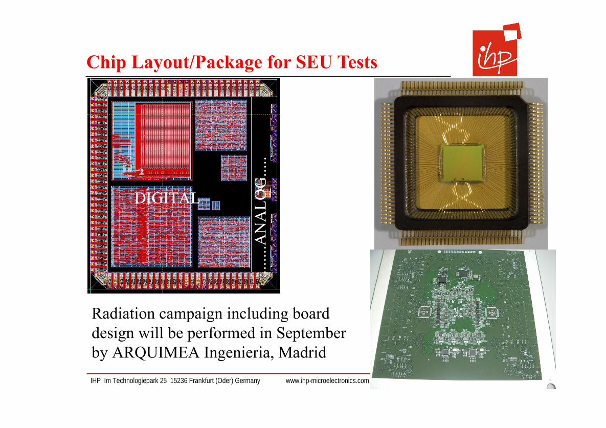
Chip Layout/Package for SEU Tests
DIGITAL
......
..AN
AL
OG
.... .
Radiation campaign including board design will be performed in September by ARQUIMEA Ingenieria, Madrid

IHP Im Technologiepark 25 15236 Frankfurt (Oder) Germany www.ihp-microelectronics.com © 2012 - All rights reserved
DIGITAL
......
..AN
AL
OG
.... .
Space projects in SGB25V/SGB25RHARQUIMEA (Spain – Prime Contractor) : “EUROPEAN LVDS DRIVER Incl. COLD SPARE CAPABILITY; DEVELOPMENT AND ESCC EVALUATION AND QUALIFICATION ” - ESA Tender AO/1-6922/11/NL/LvH.”Project Consortium :Design and Programme Management : ARQUIMEA (Spain)Technology Provider : IHP (Germany)Assembly House : Micross (UK)Test House : Alter Technology Group (Spain)
Full Duration : 30 Months (for Phase I to Phase III)
Objective : Rad-Hard LVDS ICs with the following functions : ● Dual LVDS Transceiver pair IC compatible to NS DS90LV049Q Automotive part.● 4x4 LVDS cross point IC compatible to TI NS65LVDS125 commercial part.
IHP Im Technologiepark 25 15236 Frankfurt (Oder) Germany www.ihp-microelectronics.com © 2012 - All rights reserved
DIGITAL
......
..AN
AL
OG
.... .
Space projects in SGB25V/SGB25RH
Space Engineering (Italy) : “HIGHLY INTEGRATED BFN USING ON CHIP MULTINODE CONCEPT” - ESA Tender AO/1-5920/08/NL/ST.”Current SiGe MMIC technology, allows the design of multinode MMICs integrating more than one beam-forming node on the same chip. The technology allows also the integration of mixed analogue/digital functions on the same chip, thus significantly reducing the complexity part count, yield and overall cost of BFNs for both multibeam reconfigurable payload/antennas and for phased array mobile terminals
Democritus University of Thrace (GREECE): Essential TeleMetry (ETM) support ASICThales Alenia Space (France) partly CNES funded, IHP as subcontractorKayser Threde/IHP (Germany): Fractional-N Synthesizer, 12 bit DAC 1.5Gsamples IHP (Germany): DLR funded, Middleware Switch
IHP Im Technologiepark 25 15236 Frankfurt (Oder) Germany www.ihp-microelectronics.com © 2012 - All rights reserved
Introduction
0.25µm BiCMOS – SGB25V/SGB25RH
- Technology description
- Evaluation Status
- Running radhard library project
- Other projects using SGB25V technology
0.13µm BiCMOS - SG13S
Outline

IHP Im Technologiepark 25 15236 Frankfurt (Oder) Germany www.ihp-microelectronics.com © 2012 - All rights reserved
SG13 Process Options
Features SG13S / SG13RH Full BiCMOS
CMOSCMOS logic Digital libraries
Passives
Interconnects 7 layer Al incl. 2µm & 3µm thick layers
Bipolar (fT/fmax/BVCE0)
High-speed HBT: 250 GHz/ 300 GHz/ 1.7 V High-voltage HBT: 50 GHz/ 130 GHz/ 3.7 V
Vdd=1.2 V, Tox=2 nm + Vdd=3.3 V, Tox=7 nm
Poly-Si resistors, MIM capacitors, MOS varactors, a.o.
IHP Im Technologiepark 25 15236 Frankfurt (Oder) Germany www.ihp-microelectronics.com © 2012 - All rights reserved
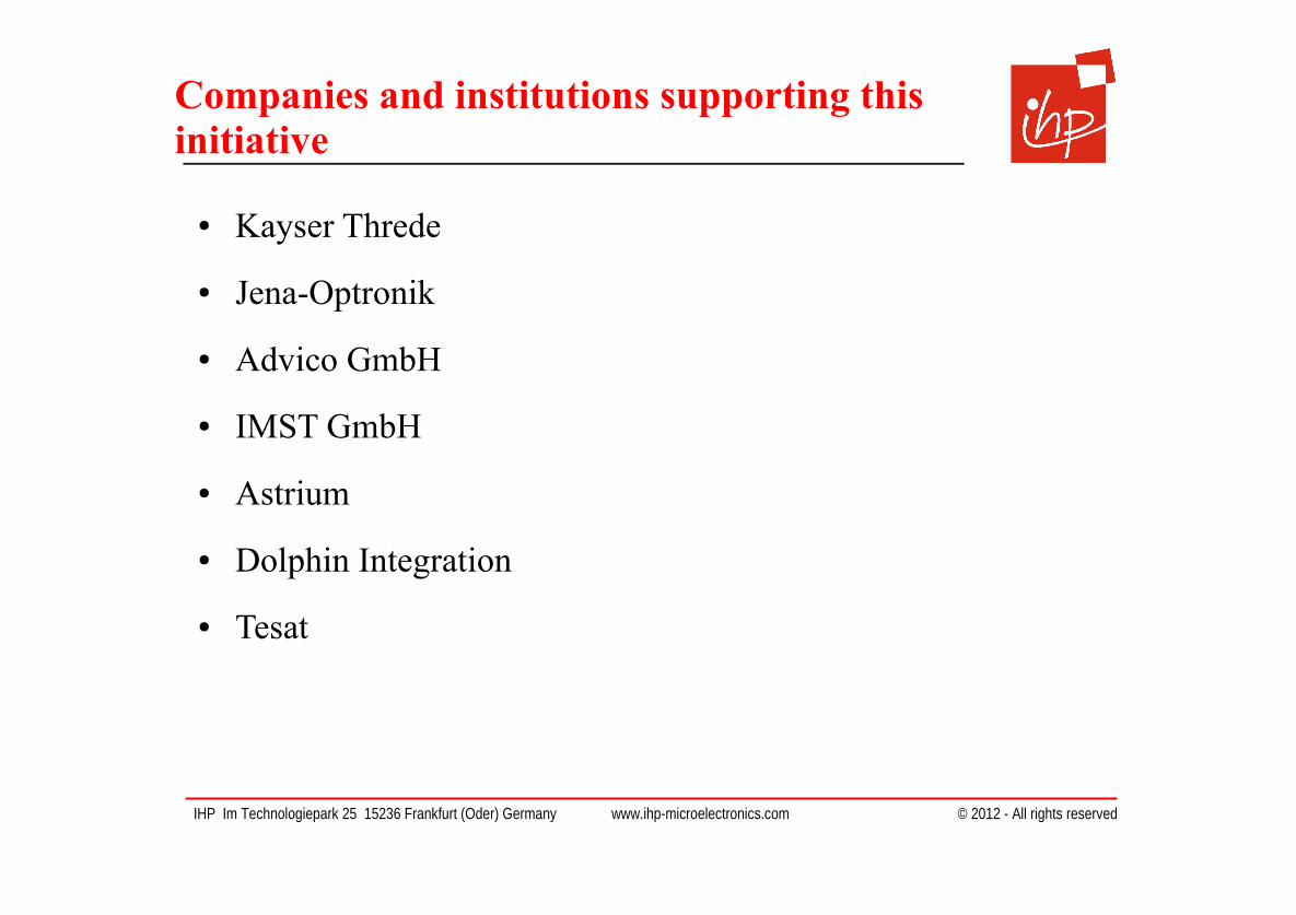
Companies and institutions supporting this initiative
● Kayser Threde
● Jena-Optronik
● Advico GmbH
● IMST GmbH
● Astrium
● Dolphin Integration
● Tesat
IHP Im Technologiepark 25 15236 Frankfurt (Oder) Germany www.ihp-microelectronics.com © 2012 - All rights reserved
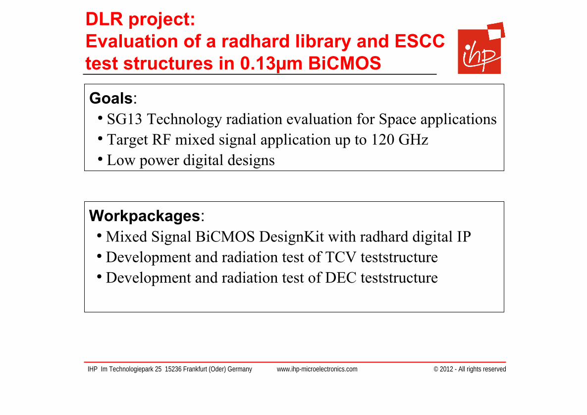
DLR project:Evaluation of a radhard library and ESCC test structures in 0.13µm BiCMOS
Goals:● SG13 Technology radiation evaluation for Space applications● Target RF mixed signal application up to 120 GHz ● Low power digital designs
Workpackages:● Mixed Signal BiCMOS DesignKit with radhard digital IP● Development and radiation test of TCV teststructure ● Development and radiation test of DEC teststructure
IHP Im Technologiepark 25 15236 Frankfurt (Oder) Germany www.ihp-microelectronics.com © 2012 - All rights reserved
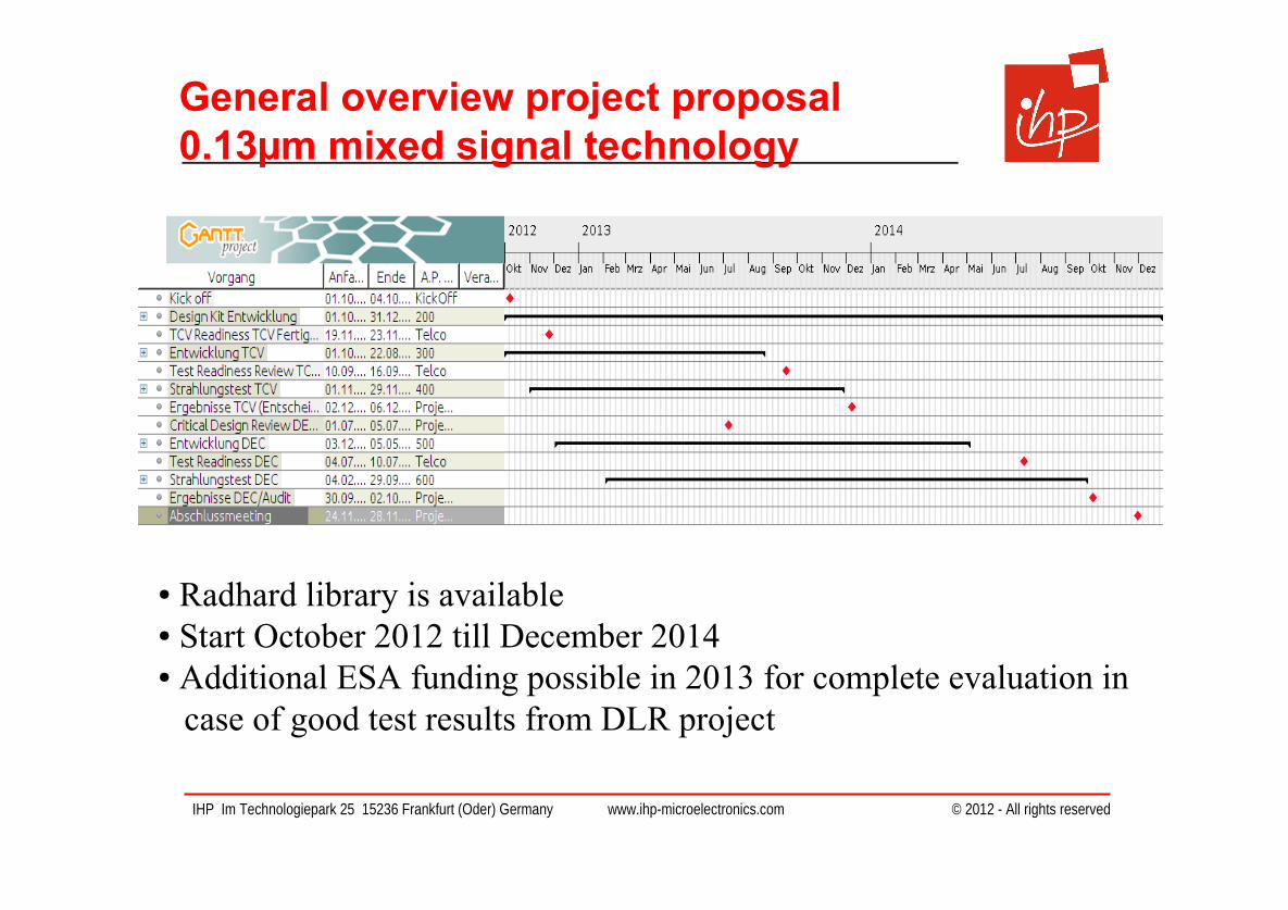
General overview project proposal 0.13µm mixed signal technology
● Radhard library is available● Start October 2012 till December 2014● Additional ESA funding possible in 2013 for complete evaluation in case of good test results from DLR project

IHP Im Technologiepark 25 15236 Frankfurt (Oder) Germany www.ihp-microelectronics.com © 2012 - All rights reserved
Conclusion
● IHP targets to offer its SiGe BiCMOS technologies as foundry service for Space applications
● Evaluation of 0.25µm BiCMOS technology nearly finalized
● Running Space Projects in 0.25µm BiCMOS
● Radhard and ESCC evaluation for 0.13µm BiCMOS will be started October 2012