ieee transactions on biomedical circuits and …mason/pubs/tbcas_oct11_l.li_packaging.pdf · cmos...
TRANSCRIPT

IEEE TRANSACTIONS ON BIOMEDICAL CIRCUITS AND SYSTEMS, VOL. 5, NO. 5, OCTOBER 2011 439
CMOS Amperometric Instrumentation and Packagingfor Biosensor Array Applications
Lin Li, Xiaowen Liu, Student Member, IEEE, Waqar A. Qureshi, Member, IEEE, andAndrew J. Mason, Senior Member, IEEE
Abstract—An integrated CMOS amperometric instrument withon-chip electrodes and packaging for biosensor arrays is pre-sented. The mixed-signal integrated circuit supports a variety ofelectrochemical measurement techniques including linear sweep,constant potential, cyclic and pulse voltammetry. Implemented in� � � CMOS, the � ���
� chip dissipates 22.5 mW for a 200kHz clock. The highly programmable chip provides a wide rangeof user-controlled stimulus rate and amplitude settings with amaximum scan range of 2 V and scan rates between 1 mV/sec and400 V/sec. The amperometric readout circuit provides ��� �
linear resolution and supports inputs up to �� �. A 2 2gold electrode array was fabricated on the surface of the CMOSinstrumentation chip. An all-parylene packaging scheme wasdeveloped for compatibility with liquid test environments as wellas a harsh piranha electrode cleaning process. The chip was testedusing cyclic voltammetry of different concentrations of potassiumferricyanide at 100 mV/s and 200 mV/s, and results were identicalto measurements using commercial instruments.
Index Terms—Biosensor array, biosensor packaging, CMOSamperometry, CMOS potentiostat.
I. INTRODUCTION
A NALYTE detection and quantification in liquid samplesplays a major role in a variety of applications, especially
in health care, environmental monitoring, industrial quality con-trol and clinical investigation. Because of the required sensi-tivity and critical importance in daily lives, these applicationsrequire robust, easy to use, efficient, and highly accurate instru-mentation systems. Miniaturized sensor arrays are capable ofparallel analysis of multiple parameters. Because of the distinctadvantages of microsystem platforms, there has been a trend tointegrate sensor arrays onto the surface of silicon chips and per-form measurement using on-chip CMOS electronics [1]–[5]. Atthe same time, there is a great opportunity to expand lab-on-chipsolutions that replace bulky benchtop sample analysis tools withsimple, low power, portable systems. The fabrication compati-bility between many bio/chemical sensor interfaces and CMOStechnology makes a CMOS circuit an outstanding candidate fora silicon-based lab-on-chip solution [6].
Manuscript received March 22, 2011; revised August 10, 2011; acceptedSeptember 19, 2011. Date of publication October 14, 2011; date of currentversion October 26, 2011. This project was supported by the National ScienceFoundation under Award DBI-0649847 and the NSF Engineering ResearchCenters Program under Award EEC-9986866. This paper was recommendedby Associate Editor Julius Georgiou.
The authors are with the Department of Electrical and Computer Engineering,Michigan State University, East Lansing, MI 48824 USA (e-mail: [email protected]).
Color versions of one or more of the figures in this paper are available onlineat http://ieeexplore.ieee.org.
Digital Object Identifier 10.1109/TBCAS.2011.2171339
Many techniques have been developed to measure analyteconcentration in solutions including electrochemical methods,optical imaging, thermal detection, spectrometry [7] and mag-netic biosensors [8]. Electrochemical methods are attractivebecause they can readily be adapted to CMOS instrumentation.The two techniques most commonly used to acquire qualita-tive information in electrochemical sensors are voltammetryand impedance spectroscopy. We have previously reporteddevelopments in CMOS voltammetry [9], [10] and impedancespectroscopy [11], [12] circuits for biosensor applications. Involtammetry, a voltage is applied to the electrochemical cell re-sulting in an output current between the counter electrode (CE)and the working electrode (WE) which is measured using anamperometric readout circuit [13]. A reference electrode (RE)is also often present in the system to stabilize solution potential.Numerous CMOS potentiostats have been introduced over thepast decade with various functionality and performance to meetdifferent applications demands. Several approaches to permitthe use of CMOS circuitry within liquid test environmentshave been reported [14]–[19]. These methods utilize epoxyadhesives or PDMS to seal the electrical wires and to createmicrofluidic structures. However, these materials cannot sur-vive extreme cleaning procedures, e.g., piranha cleaning, whichare often required to clean electrode surfaces before biosensorinterface formation. Furthermore, epoxy encapsulation hasreliability issues due to poor adhesion to the chip substrate,stress imposed on wire bonds, and lack of an accurate align-ment method. Another approach reported the use of paryleneas the encapsulation material [20]. However, the micromachinglaser source used to ablate the parylene during patterning ishard to control and potentially damaging to the sensing regionunderneath, and the ultrasonic bath used to lift-off the parylenecould compromise sealing around the wire bonds.
Fully integrated electrochemical microsystems for DNAand detection of bacteria and biomolecules have been re-ported [21]–[26], but these systems do not provide all thefeatures needed for nanostructured protein interfaces [12]targeted by this work, such as the necessity for extremelyclean and flat electrodes. This paper reports a complete, singlechip electrochemical instrumentation system with a broadcurrent range amperometric readout circuit and a digitallyprogrammable voltage waveform generator supporting a di-verse set of electrochemical techniques. The multi-functionamperometric instrumentation chip (MAIC) includes a 2 2array of single-ended potentiostats and amperometric readoutcircuits and a waveform generator that produces triangular,saw tooth, constant potential and square pulse signals for
1932-4545/$26.00 © 2011 IEEE

440 IEEE TRANSACTIONS ON BIOMEDICAL CIRCUITS AND SYSTEMS, VOL. 5, NO. 5, OCTOBER 2011
cyclic, linear sweep, constant potential and pulse voltammetrytechniques, respectively. Furthermore, this paper introduces achip-scale integration scheme for protein-based biosensors andelectrochemical circuitry utilizing post-CMOS microfabrica-tion including on-chip flat microelectrode array fabrication andpackaging for liquid environments and harsh chemical cleaning.These post-CMOS fabrication processes were applied to anMAIC chip to form a 2 2 array of gold electrodes suitable forformation of protein biointerfaces. A unique parylene-basedchip-in-package scheme is also introduced, providing excel-lent biocompatibility, reliable insulation for long-term use inliquids, and resistance to aggressive chemical cleaning.
The system architecture for the CMOS electrochemicalsensor array is discussed in Section II. The CMOS electro-chemical instrumentation circuitry is presented in Sections IIIand IV describes the post-CMOS electrode microfabricationand packaging. Finally, test results are presented in Section V.
II. SYSTEM ARCHITECTURE
A. CMOS Electrochemical Instrumentation
Electrochemical amperometry techniques such as cyclicvoltammetry (CV) are often employed to characterizebiosensor interface properties. Such techniques can readilybe implemented within CMOS instrumentation circuits. Forexample, our group has previously reported CMOS readoutelectronics including a compact potentiostat that supports avery broad range of input currents, 6 pA to [10]. Aprototype electrochemical sensor platform utilizing this chipand a miniaturized biosensor array was characterized usingcyclic voltammetry. Our group also reported a CMOS bi-po-tentiostat and amperometric readout chip that uses a commonpotential control unit and two readout channels to implementredox recycling to amplify electrochemical currents [27]. Thesesuccessful circuits provide the foundation for the chip-scalesystem integration described in this paper.
B. CMOS Electrochemical Array System Concept
The chip-scale miniaturization and integration of electro-chemical sensors and their instrumentation electronics hasmany advantages. Through miniaturization of electrodes, thelimits of detection can be extended by improving the signal tonoise ratio. The direct, on-chip, electrical connection of elec-trodes to the instrumentation circuit eliminates external wiringand provides immunity from environmental interference. Thisnoise reduction permits highly sensitive circuits to measurethe responses of miniature biosensors, allowing a high-densitysensor array within the small platform of a CMOS chip.
Many semiconductor devices and fabrication processes arecompatible with biological materials, enabling the expandinguse of these technologies for devices such as neural probes andbiosensor arrays. Combining CMOS instrumentation circuitswith miniaturized electrode arrays fabricated on CMOS chipsintroduces the opportunity for a monolithic measurementsystem. Fig. 1 illustrates the electrochemical biosensor arraymicrosystem that serves as the conceptual model for the work inthis paper. A CMOS electrochemical instrumentation chip actsas the substrate of the microsystem. An array of gold electrodes
Fig. 1. Conceptual illustration of a CMOS circuit with on-chip electrode arrayand packaging for use in a liquid environment.
fabricated post-CMOS on the surface of the chip are connectedthrough overglass contact openings to the underlying CMOSelectronics. These electrodes must be clean and smooth tosupport formation of biosensor interfaces on electrode surfaces.Because the surface is uneven at overglass openings, electrodeareas are defined away from overglass contacts and connectedby surface metal routing. This approach also provides flexibilityin the placement of surface contacts that lessens CMOS layoutconstraints, and it permits modification of electrode patternswithout redesigning the underlying CMOS chip. To insulatesurface metal routing and define size-adjustable openingsover individual electrodes, a passivation layer is applied aftermetallization. This insulation layer also planarizes the surfaceand provides an interface to a variety of possible fluid handlingschemes, including microfluidics or the simple liquid reservoirillustrated in Fig. 1. Alternatively, the entire chip, includingwirebonds, could be coated with an insulating material asdescribed in this paper.
The Fig. 1 electrochemical microsystem concept can beadapted to a wide range of biosensor interfaces. In this work,we have targeted protein-based nanostructured biointerfacesthat can be self assembled on electrodes [12]. These nano-scaleinterfaces permit rapid response but impose additional mi-crosystem design constraints, chiefly the necessity for anelectrode that is flat and smooth to the nano scale.
III. CMOS DESIGN
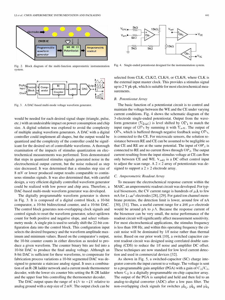
For an autonomous microsystem, the CMOS chip would in-clude all necessary instrumentation electronics and a commu-nication interface to allow user control of measurement opera-tions and reporting of measurement results. For the multi-func-tion amperometric instrumentation chip (MAIC), this requires apotentiostat to control electrode biasing, a multi-function wave-form generator to produce the stimulus signals necessary forvoltammetry techniques, and a highly sensitive amperometricreadout circuit to measure the current resulting from the stim-ulus voltage. Fig. 2 illustrates this arrangement of componentsand serves as the system diagram for the MAIC.
A. Programmable Waveform Generator
A waveform generator is an important component of an au-tonomous electrochemical instrumentation system that requiresdifferent input waveforms for different voltammetry techniques.A multi-mode waveform generator is desired to produce sig-nals of various shapes, amplitudes (scan range) and frequencies(scan rates). Programmable analog circuits could be constructedto generate continuous waveforms, but different analog circuits
LI et al.: CMOS AMPEROMETRIC INSTRUMENTATION AND PACKAGING 441
Fig. 2. Block diagram of the multi-function amperometric instrumentationsystem.
Fig. 3. A DAC-based multi-mode voltage waveform generator.
would be needed for each desired signal shape (triangle, pulse,etc.) with an undesirable impact on power consumption and chipsize. A digital solution was explored to avoid the complexityof multiple analog waveform generators. A DAC with a digitalcontroller could implement all shapes, but the output would bequantized and the complexity of the controller could be signif-icant for the desired set of controllable waveforms. A thoroughexamination of the impacts of stimulus quantization on elec-trochemical measurements was performed. Tests demonstratedthat steps in quantized stimulus signals generated noise in theelectrochemical output current, but the noise reduced as stepsize decreased. It was determined that a stimulus step size of8 mV or lower produced output results comparable to contin-uous stimulus signals. It was also determined that, with carefuldesign, a very efficient digitally controlled waveform generatorcould be realized with low power and chip area. Therefore, aDAC-based multi-mode waveform generator was developed.
The digitally programmable waveform generator is shownin Fig. 3. It is composed of a digital control block, a 10-bitcomparator, a 10-bit bidirectional counter, and a 10-bit DAC.The control block generates non-overlapping clock signals andcontrol signals to reset the waveform generator, select up/downcount for both positive and negative slope, and select voltam-metry mode. A single pin is used to serially shift the 22-bit con-figuration data into the control block. This configuration inputselects the desired frequency and the waveform amplitude max-imum and minimum values. Based on the comparator’s output,the 10-bit counter counts in either direction as needed to pro-duce a given waveform. The counter binary bits are fed into a10-bit DAC to produce the final analog voltage. Although an8-bit DAC is sufficient for these waveforms, to compensate forfabrication process variations a 10-bit segmented DAC was de-signed to generate a staircase analog signal. It uses a combina-tion of an R-2R ladder network and a current mode thermometerdecoder, with the lower six counter bits setting the R-2R ladderand the upper four bits controlling the thermometer decoder.
The DAC output spans the range of to relative toanalog ground with a step size of 2 mV. The output clock can be
Fig. 4. Single-ended potentiostat designed for the instrumentation system.
selected from CLK, CLK/2, CLK/4, or CLK/8, where CLK isthe external input master clock. This provides a stimulus signalup to 2 V pk-pk, which is suitable for most electrochemical mea-surements.
B. Potentiostat Array
The basic function of a potentiostat circuit is to control andmaintain the voltage between the WE and the CE under varyingcurrent conditions. Fig. 4 shows the schematic diagram of the3-electrode single-ended potentiostat. Output from the wave-form generator is level shifted by to match theinput range of by summing it with . The output of
, which is buffered through negative feedback using ,is connected to the CE. For microscale sensors, the solution re-sistance between RE and CE can be assumed to be negligible sothat CE and RE are at the same potential. The input of isconnected to RE and no current flows through . The outputcurrent resulting from the input stimulus voltage at CE can flowonly between CE and WE. is a DC offset control inputto adjust the scan range. A 2 2 array of potentiostats was de-signed to support a 2 2 electrode array.
C. Amperometric Readout Array
To measure the electrochemical response current within theMAIC, an amperometric readout circuit was developed. For typ-ical biosensors, the CV current range is hundreds of to fewmA for electrodes [28], [29]. For gated ion channel mem-brane proteins, the detection limit is lower, around few of nA[30], [31]. Thus, a useful current range for a electrodewould be around pA to . Because the response current ofthe biosensor can be very small, the noise performance of thereadout circuit will significantly affect measurement sensitivity.For most electrochemical applications, the stimulus frequencyis less than 100 Hz, and within this operating frequency the cir-cuit noise will be dominated by 1/f noise rather than thermalnoise. Based on our prior work [10], a switched capacitor cur-rent readout circuit was designed using correlated double sam-pling (CDS) to reduce the 1/f noise and amplifier DC offset.These techniques are now standard for low level current detec-tion and used in commercial devices [32].
As shown in Fig. 5, a switched-capacitor (SC) charge inte-grator converts the input current to a voltage. The voltage is sentto a programmable gain amplifier (PGA) with a gain of ,where is a digitally programmable on-chip capacitor array.The output of the PGA is sampled and held and then fed to ananalog-to-digital converter (ADC) after a low pass filter. Thenon-overlapping clock signals for switches , and

442 IEEE TRANSACTIONS ON BIOMEDICAL CIRCUITS AND SYSTEMS, VOL. 5, NO. 5, OCTOBER 2011
Fig. 5. Schematic of amperometric readout circuit.
are generated by an on-chip clock generator block. The outputvoltage of the current readout circuit is given by
(1)
where is the current at the WE and is the frequencyof switch , is the integrating capacitor. Thus, the inputcurrent range can be adjusted to output of different biosensorsthrough programmable selection of the clock frequency and thePGA gain. These programmable features can be used to cali-brate sensors over time.
Several improvements have been implemented in the newreadout circuit to increase measurement sensitivity. In theCDS technique, the noise reduction factor is typically deter-mined by device matching, timing errors, charge injection andclock feedthrough. To curtail charge injection, all switcheswere realized with minimum size transistors. To reduce clockfeedthrough errors, the NMOS switches were replaced by astructure with one NMOS switch and two NMOS dummy tran-sistors. An on-chip clock generator was developed to provideprecise time sequence control for switch activation.
Noise in the amplifier also directly affects the sensitivity ofthe readout circuit. A folded cascode amplifier was chosen be-cause it provides high DC gain and wide dynamic range. Ac-cording to the noise analysis in [10], the size of the input tran-sistors is critical. Increasing the value of WL and W/L can re-duce the 1/f noise and thermal noise. However, larger inputtransistors will lead to larger input bias current, which limitsthe sensitivity of the readout circuit. An input bias current ofhundreds of fA at was reported for an input NMOS of
[10]. To optimize the tradeoff betweennoise, speed and input bias current, this design sets
for the NMOS inputs transistors. To further im-prove noise performance, all of the analog circuits were sur-rounded by capacitors between and GND to minimizepower supply noise, and the analog and digital power routingswere separated over the whole chip to minimize digital clocknoise coupling onto analog signals. Through these improve-ments, the sensitivity was increased by a factor of six comparedto prior work [10].
IV. POST-CMOS ELECTRODE ARRAYS AND PACKAGING
Realizing a single-chip biosensor array with embeddedinstrumentation circuitry requires the synergistic integration
of CMOS design, electrode fabrication and packaging whilesimultaneously meeting requirements set by 1) IC processcompatibility, 2) biointerface self assembly, 3) electrochemicalanalysis capability and 4) operation in a liquid environment.Fabrication processes such as metal vapor and chemical vapordeposition, wet chemical and plasma dry etching, and pho-tolithography maintain the reliability of active circuits withinthe CMOS substrate when conducted at temperatures lowerthan [33], forming a limited microfabrication tools set.Similarly, requirements for biointerface assembly and operationin a liquid environment constrain the materials and structuresavailable for electrodes and packaging. To meet these complexconstraints, a scheme combining electrode fabrication and chippackaging was developed that utilizes complementary die-leveland package-level process steps.
A. Insulation and Packaging Materials
Operation of the CMOS biosensor array in an aqueous en-vironment establishes a critical requirement to insulate all sur-faces of the CMOS device in contact with the liquid. The smallsurface area available on a CMOS chip necessitates either acomplex fluid handling system or packaging of the entire chipfor immersion in liquid. Because the chip’s surface must re-main accessible for biointerface formation and sensor operation,flip-chip packaging and other approaches that similarly buryI/O bondpads cannot be employed in a straightforward manner.Alternatively, a chip-in-package approach utilizing wirebondeddie was adopted in this work, establishing a need for a protectiveinsulating material capable of coating all surfaces of the 3D chipstructure, including chip sidewalls and wirebonds. At the sametime, the packaging approach must permit patterning of the 2Dchip-electrode surface and cleaning of electrodes to remove anymetal ions or contaminants before biointerface assembly. Forexample, our experiments have shown that aggressive electrodecleaning by piranha solution and organic cleaning are requiredfor reliable self assembly of nanostructured biointerfaces. Thepackaging material must therefore withstand the strong corro-siveness of piranha solution. Several materials were studied tomeet these demands.
SU-8 photoresist is widely used in MEMS fabrication; it isavailable in a wide range of viscosities and is suitable to formthick layers and high aspect ratio structures [34]. However,when tested experimentally, cracks were observed after pro-longed soaking in an aqueous environment. Fig. 6(a) shows aCMOS chip with a thick SU-8 passivation layer, and Fig. 6(b)shows cracks that developed near the pad area and causedcorrosion of the bonding pads that rendered the chip useless.
Polyimide is another insulating polymer material widelyused in bioMEMS packaging applications, although it cannotachieve layers as thick as SU-8. Polyimide can be appliedby spin coating and curing in a low temperature oven. It iseasy to pattern using either wet or dry etching, and our testsindicate it provides excellent coverage and uniformity on 2Dflat surfaces and survives prolonged use in an aqueous envi-ronment. However, when tested for coverage of 3D structureslike a wirebonded chip, cracks in the polyimide layer dueto shrinkage during curing were observed. Fig. 6(c) shows apolyimide-coated CMOS chip with large cracks (light color

LI et al.: CMOS AMPEROMETRIC INSTRUMENTATION AND PACKAGING 443
Fig. 6. (a) A CMOS chip packaged using SU8 with electrodes exposed.(b) A crack in SU8 observed at the interface of the chip and SU8 where leakageoccurs. (c) A polyimide coating on the surface of a packaged chip that crackedafter hard baking.
within the dotted line) where the polyimide layer approacheswirebonds on the chip’s periphery (dark color within dottedline).
Parylene, or poly (p-xylylene), is a thin film polymer thatis also popular for insulating electronics. Parylene is chemi-cally inert, permits conformal coating and has excellent bar-rier properties. Parylene C (poly(monochloro-p-xylylene)) hasthe highest possible biocompatibility rating among polymers forlong term implants and has an extensive history of use in themedical industry. Because of its biocompatibility, biostability,low cytotoxicity and resistance against hydrolytic degradation,Parylene C has been widely used in micro/nano-fabricated de-vices and microfluidics. Parylene C utilizes a simple chemicalvapor deposition method with low process temperature and iscompatible with standard microfabrication processes. Our ex-periments have shown that parylene successfully overcomes theproblems associated with SU-8 and polyimide, providing anexcellent and long-lasting coating of 3D structures like wire-bonded chips.
B. CMOS Design for Surface Electrodes
The amperometric instrumentation circuit described abovewas designed in 3M, 2P, CMOS and implemented on a
chip. The chip layout includes overglass openingsthat permit connection between CMOS metals and an arrayof electrodes formed directly on the surface of the chip usingpost-CMOS processing. These contact openings are placedaway from the desired electrode area so that the electrodesurface can remain flat without a metal planarization step. Tosupport self assembly of nanostructured protein interfaces, thesurface electrodes must be flat to the scale of nanometers. Be-cause the CMOS process is not planarized following depositionof the top metal, the circuit was routed without the top CMOSmetal layer to ensure a flat chip surface for electrode formation.
C. Die-Level Fabrication
To form an on-chip microelectrode array, gold is an out-standing metal because it can readily be deposited andpatterned, is inert and biocompatible in a biosensing liquidenvironment, and permits immobilization of biointerfaces usingwell established adhesion chemistry. The on-chip electrodecould be fabricated using an electroless nickel immersiongold process that replaces the aluminum layer from a standardCMOS process [35]. However, the deposition thickness of goldis difficult to control with this method due to its depositionmechanism, and the process is prone to poor reproducibility
Fig. 7. Single element of an electrode array consisting of WE, RE and CE.
because of variable aluminum alloy composition across a chipand between different chips. Our experimental efforts withthis deposition process have resulted in a non-uniform goldlayer with high surface roughness. Alternatively, the on-chipmicroelectrode array could be fabricated using conventionalphysical vapor deposition (PVD) and photolithography, whichprovides precise control of electrode thickness and area. Withthis method, the roughness of the gold is subject to the surfaceprofile of the CMOS chip, which is typically passivated by aflat silicon dioxide layer. For many protein-based biosensors,the electrode roughness is a critical parameter. For example,a biosensor utilizing a biomimmetic tethered lipid bilayermembrane [12] must have a very smooth surface to preventpinholes in the self assembled lipid bilayer.
To enable electrochemical measurement, each element of theon-chip array includes a WE, CE and RE. Development of a re-liable planar reference electrode remains a research challenge,and a pseudo RE was chosen so that all electrodes could beformed using Au. Fig. 7 describes the electrode pattern that wasdesigned to maximize the electrochemical response current andrealize uniform ion flow by arranging the electrodes concentri-cally. The distance between WE and CE is kept small to mini-mize errors due to potential drop in the solution. The workingelectrode is relatively large to maximize sensor area, and thesize can easily be modified to suit different biosensor interfacesbased on the electrochemical current level (which is a functionof WE area) and desired array density.
The die-level post-CMOS fabrication process begins withformation of the electrode array on the CMOS MAIC chip. Werefer to this as die-level processing because we receive fromthe foundry and process individual die, but the same processescan be applied at a wafer scale. The electrodes are formedby thermal evaporation of titanium/gold (50 Å/1000 Å) andpatterning by wet etching. This metallization step also createsrouting between electrodes and surface contacts to CMOSelectronics, and it covers all surface CMOS metal, includingbondpads, to eliminate chemical reactions between the CMOSaluminum alloy and the alkali photoresist developer, which hasbeen observed to contaminate the surface electrodes. Polyimideis then spin coated on the CMOS chip surface and patternedto insulate surface routings and define the electrode area whileleaving bonding pads open for subsequent wire bonding. Poly-imide was chosen because it provides good coverage of 2Dsurfaces and is much easier to pattern than the parylene appliedlater in the package process. The die-level process steps are

444 IEEE TRANSACTIONS ON BIOMEDICAL CIRCUITS AND SYSTEMS, VOL. 5, NO. 5, OCTOBER 2011
Fig. 8. Process flow for post-CMOS electrode fabrication: (a-b) Ti/Au is de-posited and patterned; (c-d) Polyimide is spin coated and patterned.
illustrated in Fig. 8. At the end of this process, the electrodearray has been formed and the chip surface has been passivatedeverywhere except the desired electrode areas and the wirebond pads.
Die-level microfabrication introduces several challenges thatare worth noting. While performing photolithography on indi-vidual die, such as the chips used in this study, pho-toresist builds up at the edge of the chip during spin coatingdue to surface tension. This leads to uneven coating across thesubstrate that makes proper exposure extremely difficulty. How-ever, we have developed a modified procedure to enable suc-cessful photolithography for die-level processing. To mitigatethick-edge effects, the chip was bonded using photoresist to theouter perimeter of a silicon wafer. This permits the die to spinat maximum speed for a given spin rate, minimizing photoresistbuildup at the edges of the chip. The orientation of the die wasobserved to have a significant impact on photoresist buildup,with more buildup on the sides parallel to the spin radius andless on the sides orthogonal to the spin radius. It was also ob-served that photoresist buildup is worse at bonding pads wherethe overglass contact openings provide a reservoir to hold pho-toresist. Thus, to provide the most uniform coating of photore-sist during die-level processing, the CMOS chip was designedto use bonding pads on only two parallel sides of the chip, andthose sides were placed orthogonal to the spin radius. In addi-tion, the electrode array was located near the center of the chipto avoid any edge buildup effects. As a result, the entire chip sur-face could be properly patterned to define the Au and polyimidelayers. The same methods can be applied to pattern any smallsubstrate for millimeter sized MEMS devices and microsystemapplications.
D. Package-Level Fabrication
To meet packaging demands while keeping cost and com-plexity low, a solution was developed using a chip-in-packageapproach, where the MAIC chip was mounted and wire bondedto a standard dual in-line package (DIP) and the package bodywas used as a liquid reservoir. Fig. 9 describes the package-levelpost-CMOS process for the chip-in-package approach. Fol-lowing the die-level processing described above, the MAIC chipwas wire bonded to a ceramic DIP package. The packaged chipwas then coated with a 5ìm layer of parylene using PVD (PDS2035CR, Specialty Coating Systems). This process covers allsurfaces within the package, including bond wires, packagecontact pads and the electrode array chip. Next, parylene needsto be removed from the electrode array area while leaving all
Fig. 9. Process flow of chip-in-package sealing for liquid environment. (a) Chipis wire-bonded to package and coated by � �� parylene. (b) A PDMS cylinderand silicon chip are attached to a glass slide and clamped to the package tocover the center of the CMOS chip before crystal adhesive is melted to fill thecavity. (c) Glass slide is detached and parylene is etched away by oxygen RIE.(d) Crystal adhesive removed to form final package with all non-electrode sur-faces insulated.
other surfaces coated. Parylene is generally etched by reactiveion etching (RIE) using oxygen gas with photoresist or anothersolid layer deposited and patterned to form a masking layer.However, in this complex three-dimensional structure, suchmethods cannot meet masking requirement, and a customized,non-traditional process was developed to overcome this chal-lenge. First, a hole punch was used to create a cylinder ofPDMS sized to match the area of the chip’s surface from whichparylene would be removed, diameter in this case.A silicon chip of slightly smaller diameter was also cut froma wafer using a dicing saw. The cylinder was then attached,on one side, to the silicon chip using oxygen plasma assistedbonding and, the other side, to a glass slide. The silicon chip wasincluded to eliminate direct contact of PDMS with parylene,which was observed to leave unwanted particle contaminantsthat were difficult to remove. The glass slide was then clampedto the parylene-coated chip-in-package with the silicon chippressed down over the electrode area. Crystal adhesive was theninserted into the cavity beneath the slides and melted atto fill the cavity except where the PDMS/silicon cylinder washeld [Fig. 9(b)]. Later, the slide/PDMS/silicon assembly wasremoved leaving parylene everywhere except the interior ofchip’s surface where previously deposited polyimide remains toinsulate surface routing and leave only the electrodes exposed.Parylene was then etched using RIE, with 300 W RF powerand 500 sccm oxygen flow rate, to expose the desired electrodesurfaces [Fig. 9(c)]. Once the crystal adhesive was removed

LI et al.: CMOS AMPEROMETRIC INSTRUMENTATION AND PACKAGING 445
Fig. 10. The ����� CMOS amperometric instrumentation chip with wave-form generator and 4-channel potentiostat and amperometric readout array.
TABLE IWAVEFORM GENERATOR CHARACTERISTICS
using acetone, the final package provides exposed electrodewith all other surfaces coated with parylene [Fig. 9(d)].
V. RESULTS
A version of the MAIC with the multi-function waveformsignal generator and a 4-channel potentiostat and amperometricreadout circuit array was fabricated in foundry CMOS.The die shown in Fig. 10 was thoroughly tested toverify functionality and characterize performance. Table I sum-marizes the characteristics of the waveform generator suitablefor various cyclic, linear sweep, constant potential and pulsevoltammetry electrochemical techniques. To characterize therange and resolution of the amperometric readout circuit, theinput current was swept using a Keithley 6430 sub-femtoampsource meter at different update clock frequencies and gainsettings to span the functional input current range. Withineach range, the maximum deviation between measured cur-rent and the linear input source was recorded as the linearityerror. Table II shows a set of test results spanning the circuit’sfunctional input range, with range settings from to
. Within each setting, the input range defines the maxcurrent before op-amps become nonlinear and create significantdistortion. The 200 Hz to 2 MHz data show that the resolutiondecreases roughly linearly with clock frequency, and at 2 kHzand above the resolution is about 0.3% of the range. Fig. 11shows test results where the maximum resolution of isachieved with gain setting of 2 at 20 Hz clock; leakage currentsprevent operation at lower frequencies. The power consumptionof the 4-channel instrumentation circuit could not be measured
TABLE IICHARACTERISTICS OF THE CURRENT READOUT CIRCUIT
Fig. 11. The deviation between input current and measured current for 1 pA to30 pA inputs at 20 Hz updating clock and gain=2 setting.
Fig. 12. Photograph of a CMOS biosensor array chip-in-package and close upviews of the post-CMOS surface electrode array.
independently of test circuits but was simulated to be 22.5 mWat a maximum clock frequency of 200 kHz.
A 2 2 electrode array was fabricated on chip, and the chipwas packaged by methods described in Section IV. The finalpackaged CMOS chip with electrode array is shown in Fig. 12.This package scheme is suitable for subsequent integrationwith microfluidic channels mounted either to the chip or to thepackage. The wire bond contact pads are the most vulnerablearea in this type of packaging. To evaluate the package sealing,the chip was powered up and successfully tested after a waterdrop was dispensed on the chip. Subsequently, the packagedchip was exposed to piranha solution to clean the electrodearray, verifying the capability to withstand the aggressive chem-ical processing necessary before protein biosensor interfaceformation on the electrodes.
To verify electrochemical measurement capability of the inte-grated system, a test setup composed of an MAIC chip, a pack-aged on-chip electrode array, and a PC with a DAQ card and a

446 IEEE TRANSACTIONS ON BIOMEDICAL CIRCUITS AND SYSTEMS, VOL. 5, NO. 5, OCTOBER 2011
Fig. 13. CV measurement of 0.5 mM potassium ferricyanide at 100 mV/s and200 mV/s for both CHI 760 commercial instrument and proposed circuit.
Fig. 14. CV measurement of potassium ferricyanide at 0.5 mM and 1 mM forboth CHI 760 commercial instrument and proposed circuit.
LabVIEW user interface was prepared. A typical electrolyte so-lution with 1 M potassium chloride and 0.5 mM potassium fer-ricyanide was prepared, and cyclic voltammetry measurementswere performed at using an on-chip WE, a commercialliquid junction Ag/AgCl RE and a platinum CE. Fig. 13 showsthe results from both a commercial potentiostat (CHI760C, CHInstruments Inc.) and the MAIC at scan rates of 100 mV/s and200 mV/s. In cyclic voltammetry, the peak locations give im-portant information for biochemical identification, and theseresults demonstrate that the peak locations and amplitudes ofthe CMOS system compare extremely well with the commer-cial system even at different scan rates. In another experiment,a second solution with 1 mM potassium ferricyanide was pre-pared and cyclic voltammetry measurements were performed.Fig. 14 shows results from both the commercial potentiostat andthe reported CMOS amperometric system at two different elec-trolyte concentrations. As expected, the peak current increasedwith electrolyte concentration, and again the peak locations andamplitudes of the CMOS system compare extremely well withthe commercial system. These experiments verify the proper op-eration of the MAIC, the functionality of the post-CMOS elec-trodes, and the suitability of the parylene-based packaging foroperation in liquid environments.
Tests were also performed to characterize the measurementvariation arising from differences in readout channels and elec-trodes across the array. Variation results will be reported as
where and are mean and standard deviation,respectively. Variations in readout channels will occur due tointra-chip process variations. When four readout channels onone chip were tested with a input current, the resultswere . Variations in electrodes could be causedby variations in the photolithography process, alignment errors,or differences in the cleanliness of electrodes. When four elec-trode on the same array were tested electrochemically, oxida-tion and reduction peak separations were found to be
. For comparison, peak separation was measured fora single electrode while sweeping the potassium ferricyanidepotential for 15 cycles, and variation in peak separation wasrecorded as . These results indicate that theobserved intra-chip variations in circuits and electrodes are lesssignificant than variations caused by electrochemical solution.
The long term stability of CMOS biosensor arrays are po-tentially limited by a) electronics, b) packaging, c) biointerface.Absent radiation and temperature extremes that are not commonto biosensor applications, CMOS electronics stability will belimited by chemical interactions with the liquid environment,which must be protected by the packaging. The reported pary-lene packaging was chosen specifically for its ability to providethis protection, and a parylene coated CMOS chip has been re-ported to remain stable in saline for more than six months[36]. Thus, stability of biosensors based on the reported CMOSarray will likely be limited by the performance of specific bioin-terfaces chosen to implement the sensor.
VI. CONCLUSION
A CMOS amperometric instrumentation system with on-chipelectrode array and packaging for biosensor arrays was pre-sented. This system can generate multiple voltage waveformswith programmable scan rates of 400 V/sec to 1 mV/sec anda scan range of 0–2 V in 2 mV steps to support a variety ofelectrochemical voltammetry techniques. The chip contains a4-channel single-ended potentiostat and amperometric readoutcircuit that was tested to provide a range andlinear resolution. A post-CMOS fabrication process was de-scribed for forming an on-chip electrode array suitable forprotein-based biosensors and parylene packaging suitable foroperation in a liquid environment. Functionality of the overallsystem was verified by performing cyclic voltammetry in apotassium ferricyanide solution. The on-chip instrumentationcircuits successfully performed electrochemical measurementsat different scan rates and electrolyte concentrations. Theinstrumentation circuitry and post-CMOS fabrication processesreported here are suitable for forming single-chip electrochem-ical analysis microsystems with a wide range of biological andchemical sensor interfaces.
ACKNOWLEDGMENT
The assistance of Dr. L. Meng and the support of the MOSISService are gratefully acknowledged.

LI et al.: CMOS AMPEROMETRIC INSTRUMENTATION AND PACKAGING 447
REFERENCES
[1] X. Zhu and C. H. Ahn, “On-chip electrochemical analysis system usingnanoelectrodes and bioelectronic CMOS chip,” IEEE Sensors J., vol.6, no. 6, pp. 1280–1287, May 2006.
[2] K. S. Yun, H. J. Kim, S. Joo, J. Kwak, and E. Yoon, “Analysis ofheavymetal ions using mercury microelectrodes and a solid-state ref-erence electrode on a Si wafer,” Jpn. J. Appl. Phys. 1, vol. 39, no. 39,pp. 7159–7163, Dec. 2000.
[3] M. S. Schienle et al., “A fully electronic DNA sensor with 128 positionsand in-pixel A/D conversion,” IEEE J. Solid-State Circuits, vol. 39, no.39, pp. 2438–2445, Dec. 2004.
[4] B. Eversmann et al., “A 128� 128 CMOS biosensor array for extra-cellular recording of neural activity,” IEEE J. Solid-State Circuits, vol.38, no. 38, pp. 2306–2317, 2003.
[5] X. Yue et al., “A real-time multi-channel monitoring system for stemcell culture process,” IEEE Trans. Biomed. Circuits Syst., vol. 2, no. 2,pp. 66–77, Jun. 2008.
[6] B. Jang and A. Hassibi, “Biosensor systems in standrard CMOS pro-cesses fact or fiction?,” in Proc. IEEE Symp. Industrial Electronics,2008, pp. 2045–2050.
[7] K. E. Gonsalves, C. L. Laurencin, C. R. Halberstadt, and L. S. Nair,Biomedical Nanostructures. New York: Wiley, 2008, p. 442.
[8] H. Wang, Y. Chen, A. Hassibi, A. Scherer, and A. Hajimiri, “A fre-quency shift CMOS magnetic biosensor array with single-bead sensi-tivity and no external maget,” in Proc. IEEE Int. Solid-State CircuitsConf., Feb. 2009, pp. 438–439.
[9] J. Zhang, Y. Huang, N. Trombly, C. Yang, and A. Mason, “Electro-chemical array microsystem with integrated potentiostat,” in Proc.IEEE Int. Conf. Sensors, Irvine, CA, Oct. 2005, pp. 385–388.
[10] C. Yang, Y. Huang, B. L. Hassler, R. M. Worden, and A. J. Mason,“Amperometric electrochemical microsystem for a miniaturized pro-tein biosensor array,” IEEE Trans. Biomed. Circuits Syst., vol. 3, no. 3,pp. 160–168, Jun. 2009.
[11] C. Yang and A. Mason, “Fully integrated 7-order frequency rangequadrature sinusoid signal generator,” IEEE Trans. Instrum. Meas.,vol. 58, no. 58, pp. 3481–3489, Oct. 2009.
[12] C. Yang, S. R. Jadhav, M. R. Worden, and A. J. Mason, “Compact lowpower impedance-to-digital converter for sensor array microsystems,”IEEE J. Solid-State Circuits, vol. 44, no. 44, pp. 2844–2855, Oct. 2009.
[13] A. J. Bard and L. R. Faulkner, Electrochemical Methods. New York:Wiley, 1980.
[14] T. Prodromakis, P. Georgiou, T. G. Constandinou, K. Michelakis, andC. Toumazou, “Batch encapsulation technique for CMOS based chem-ical sensors,” in Proc. IEEE Biomedical Circuits and Systems Conf.,Oct. 2008, pp. 321–324.
[15] W. Oelßner et al., “Encapsulation of ISFET sensor chips,” Sens. Actu-ators B, Chem., vol. 105, no. 105, pp. 104–117, 2005.
[16] E. Ghafar-Zadeh, M. Sawan, and D. Therriault, “Novel direct-writeCMOS-bsed laboratory-on-chip design, assembly and experimental re-sults,” Sens. Actuators A, Phys., vol. 134, no. 134, pp. 27–36, Feb. 2007.
[17] U. Frey et al., “Switch-matrix-based high-density microelectrode arrayin CMOS technology,” IEEE J. Solid-State Circuits, vol. 45, no. 45, pp.467–482, 2010.
[18] C. Dumschat et al., “Encapsulation of chemically sensitive field-effecttransistors with photocurable epoxy resins,” Sens. Actuators B, Chem.,vol. 2, no. 2, pp. 271–276, 1990.
[19] J. M. B. Christen and A. G. Andreou, “Design, fabrication, and testingof a hybrid CMOS/PDMS microsystem for cel lculture andincubation,”IEEE Trans. Biomed. Circuits Syst., vol. 1, no. 1, pp. 3–18, Mar. 2007.
[20] T. Prodromakis, K. Michelakis, T. Zoumpoulidis, R. Dekker, and C.Toumazou, “Biocompatible encapsulation of CMOS based chemicalsensors,” in Proc. IEEE Int. Conf. Sensors, Oct. 2009, pp. 791–794.
[21] R. Popovtzer et al., “Novel integrated electrochemical nano-biochip fortoxicity detection in water,” Nano Lett., vol. 5, no. 5, pp. 1023–1027,2005.
[22] A. Frey et al., “A digital CMOS DNA chip,” in Proc. IEEE Int. Symp.Circuits and Systems, 2005, vol. 3, pp. 2915–2918.
[23] S. Hwang et al., “CMOS microelectrode array for electrochem-ical lab-on-a-cihp applications,” IEEE J. Sensors, vol. 9, no. 9, pp.609–615, Jun. 2009.
[24] P. M. Levine, P. Gong, R. Levicky, and K. L. Shepard, “Active CMOSsensor array for electrochemical biomolecular detection,” IEEE J.Solid-State Circuits, vol. 43, no. 43, pp. 1859–1871, Aug. 2008.
[25] A. Hassibi and T. H. Lee, “A programmable 0.18-um CMOS electro-chemical sensor microarray for biomolecular detection,” IEEE J. Sen-sors, vol. 6, no. 6, pp. 1380–1388, Dec. 2006.
[26] P. Kruppa et al., “A digital CMOS-based 24� 16 sensor array platformfor fully automatic electrochemical DNA detection,” Biosen. Bioelec-tron., vol. 26, no. 26, pp. 1414–1419, 2010.
[27] Y. Huang and A. J. Mason, “A redox-enzyme-based electrochemicalbiosensor with a CMOS integrated bipotentiastat,” in Proc. IEEEBiomedical Circuits Systems Conf., Beijing, China, Nov. 2009, pp.29–32.
[28] D. Grieshaber, R. MacKenzie, J. Voros, and E. Reimhult, “Electro-chemical biosensors—sensor principles and architectures,” Sens. Ac-tuators B, Chem., vol. 8, no. 8, pp. 1400–1458, 2008.
[29] M. Zhang, A. Smith, and W. Gorski, “Carbon nanotube-chitosansystem for electrochemical sensing basd on dehydrogenase enzymes,”Anal. Chem., vol. 76, no. 76, pp. 5045–5050, 2004.
[30] S. R. Jadhav, D. Sui, M. R. Garavito, and M. R. Worden, “Fabricationof highly insulating tethered bilayer lipid membrane using yeast cellmembrane fractions for measuring ion channel activity,” J. Colloid In-terface Sci., vol. 322, no. 322, pp. 465–472, 2008.
[31] P. Krysinski et al., “Tethered mono- and bilayer lipid membranes onAu and Hg,” Langmuir, vol. 17, no. 17, pp. 3852–3857, 2001.
[32] Texas Instruments, DDC 118: Octal current Input, 20-bit Analog-to-Digital Converter, 2009.
[33] S. M. Martin, F. H. Gebara, B. J. Larivee, and R. B. Brown, “A CMOS-integrated microinstrument for trace detection of heavy metals,” IEEEJ. Solid-State Circuits, vol. 40, no. 40, pp. 2777–2786, Dec. 2005.
[34] X. Liu, L. Li, and A. J. Mason, “Thermal control microsystem for pro-tein characterization and sensing,” in Proc. IEEE Biomedical CircuitsSystems Conf., Beijing, China, Nov. 2009, pp. 277–280.
[35] A. Manickam, A. Chevalier, M. McDermott, A. D. Ellington, and A.Hassibi, “A CMOS electrochemical impedance spectroscopy(EIS)biosensor array,” IEEE. Trans. Biomed. Circuits Syst., vol. 4, no. 4,pp. 379–390, Dec. 2010.
[36] W. Li et al., “Wafer-level parylene packaging with integrated RFelectronics for wireless retinal prostheses,” IEEE J. Microelectromech.Syst., vol. 19, no. 19, pp. 735–742, Aug. 2010.
Lin Li received the B.S. degree in electrical engi-neering from Tsinghua University, Beijing, China, in2006.
Currently, he is working toward the Ph.D. de-gree in electrical engineering at Michigan StateUniversity (MSU), East Lansing. From 2006 to2008, he studied EWOD microfluidics and energyharvesting by PZT and electromagnetics at theUniversity of Missouri-Columbia. In 2008, he joinedthe Advanced Microsystems and Circuits laboratoryat MSU as a Research Assistant. His Ph.D. research
includes CMOS on-chip electrochemical biosensor arrays, CMOS packaging,3D packaging, and microfluidics.
Xiaowen Liu (S’10) received the B.S. and M.S. de-grees in electrical engineering from Hefei Universityof Technology, Hefei, China, in 2002 and 2005, re-spectively.
Currently, she is working toward the Ph.D. degreein electrical engineering at Michigan State Univer-sity, East Lansing. From 2005 to 2007, she was anAnalog Design Engineer at the Beijing Microelec-tronic Technology Institute, Beijing, China, whereshe was involved in the design of high frequencyPLL frequency synthesizers. Her research interest
includes the analog and mixed-signal integrated circuit design, biomedicalelectronics, and biomedical integrated microsystems.
448 IEEE TRANSACTIONS ON BIOMEDICAL CIRCUITS AND SYSTEMS, VOL. 5, NO. 5, OCTOBER 2011
Waqar A. Qureshi (M’08) received the B.Scdegree with honors in electrical engineering fromNWFP University of Engineering and Technology,Peshawar, Pakistan, and the M.S degree in electricalengineering from Michigan State University, EastLansing, in 2004 and 2010, respectively.
Currently, he works at Institute of Applied Tech-nologies (IAT), Islamabad, Pakistan, as Manager ofAnalog/Mixed Signal IC Design. His research inter-ests include low power analog/mixed-signal IC de-sign for bio/electrochemical and image sensor inter-
faces.
Andrew J. Mason (S’90–M’99–SM’06) receivedthe B.S. degreee in physics with highest distinc-tion from Western Kentucky University, BowlingGreen, in 1991, the BSEE degree with honors fromthe Georgia Institute of Technology, Atlanta, in1992, and the M.S and Ph.D. degrees in electricalengineering from The University of Michigan, AnnArbor, in 1994 and 2000, respectively.
From 1999 to 2001, he was an Assistant Professorat the University of Kentucky, Lexington. In 2001,he joined the Department of Electrical and Computer
Engineering, Michigan State University (MSU), East Lansing. Currently,he is an Associate Professor at MSU. His research addresses many areas ofmixed-signal circuit design and the fabrication of integrated microsystems.Current projects include compact low-power bioelectrochemical interrogationcircuits, adaptive chemical sensor interface circuits, post-CMOS fabrication ofelectrochemical sensor arrays, and mixed-signal integrated circuits for signalprocessing in neural implants.
Dr. Mason serves on the Sensory Systems and Biomedical Circuits and Sys-tems Technical Committees of the IEEE Circuits and Systems Society and on thetechnical program committee for several IEEE conferences and workshops. Heis an Associate Editor of the IEEE TRANSACTIONS ON BIOMEDICAL CIRCUITS
AND SYSTEMS and co-General Chair for the 2011 IEEE BioCAS Conference. Heis a recipient of the 2006 MSU Teacher-Scholar Award and the 2010 WithrowAward for Teaching Excellence.