ieee transaction on power electronics regular paper …
TRANSCRIPT
0885-8993 (c) 2021 IEEE. Personal use is permitted, but republication/redistribution requires IEEE permission. See http://www.ieee.org/publications_standards/publications/rights/index.html for more information.
This article has been accepted for publication in a future issue of this journal, but has not been fully edited. Content may change prior to final publication. Citation information: DOI 10.1109/TPEL.2021.3063931, IEEETransactions on Power Electronics
IEEE TRANSACTION ON POWER ELECTRONICS REGULAR PAPER
An Effective Integration of APM and OBC with Simultaneous Operation and Entire ZVS Range for
Electric Vehicles
Gibum Yu, Student Member, IEEE, and Sewan Choi, Fellow, IEEE
Abstract- This paper proposes an effective integration of APM and OBC providing simultaneous operation without extra circuit and entire ZVS range of all switches. The integrated circuit of the proposed charger is configured by combining high voltage-side switch legs of the LLC resonant converter of OBC and the PSFB converter of APM. In the simultaneous mode, by operating the common leg as a lagging leg of the phase-shift full bridge (PSFB) converter, the conduction losses of the common leg switches are decreased due to current cancellation effect, and the lagging leg switches of the PSFB converter achieves entire ZVS operation. Further, in the APM standalone mode, entire ZVS operation of the lagging leg switches is also secured by utilizing magnetizing current of the LLC resonant converter. As a result, the proposed integrated charger achieves comprehensive improvement in terms of efficiency as well as volume and cost. A laboratory prototype combining a 3.7kW LLC resonant converter with a 1kW PSFB converter is built and tested in order to verify the performance and theoretical claims.
Index Terms – Integrated EV charger, LLC resonant converter, PSFB converter, soft switching, high efficiency, variable dc-link control.
I. INTRODUCTION
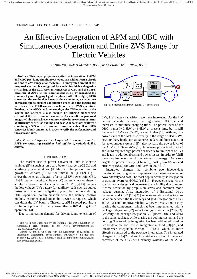
The market size of power conversion units in electric vehicles (EVs) such as on-board battery chargers (OBCs) and auxiliary power modules (APMs) will be proportional to growth of EV sales (2.1 Million units in 2019)[1]-[2]. Fig. 1 shows the schematic diagram of a typical EV power train. OBC [3]-[8] charges the high voltage (HV) battery wherever there is an electric power outlet available, and APM [9]-[13] charges the low voltage (LV) battery for auxiliary loads such as audio, instrument panel and navigation system. Furthermore, during OBC operation, communication with the battery control module, instrument panel and mobile devices is required, which can drain the LV battery. Therefore, APM should provide a continuous power of usually lower than 400W during OBC operation [14].
Due to increasing demand for driving range extension of
EVs, HV battery capacities have been increasing. As the HV battery capacity increases, the high-power OBC demand increases to minimize charging time. The power level of the OBC is mostly 3.3kW or 6.6kW at present time, but it will increase to 11kW and 22kW, or even higher [15]. Although the power level of the APM is currently in the range of 1kW-2kW, new auxiliary loads such as cameras, radars and light detection for autonomous system in EV also increase the power level of the APM up to 3kW- 4kW [16]. Increasing power level of OBC and APM requires high-power density due to limit space of EVs and leads to additional cost and power losses. In order to fulfill these requirements, the US department of energy (DoE) sets targets of power density (4.6kW/L), cost (35-40$/kW) and efficiency (98%) for OBC and APM in 2025 [17].
Integrated chargers that combine two independent functionalities using same components provide improvement of power density and cost. The most popular concept is integration of traction inverter and OBC [18]-[19]. However, it requires the special motor design and decreases the reliability due to motor lifetime reduction by propulsion stress and common mode leakage current. Also, integration of bidirectional dc-dc converter and OBC [20]-[21] reduces reliability due to non-isolation between the HV battery and grid. Integration of OBC and APM could improve reliability, power density and cost by sharing the components, which has been implemented with a package integration [22] or a topology integration [23]-[33]. Basically, the package integration [22] places OBC and APM to the same package, while sharing the cooling system and the housing. The topology integration has been addressed based on two kinds of methods; switch integration method [23]-[29] and transformer integration method [30]-[33], which is more effective compared to the package integration. The integrated chargers in [23]-[24] share full-bridge switches of the ac-dc converter of the OBC with primary switches of the APM.
Fig. 1. Schematic diagram of typical EV power train.
This work was supported by the National Research Foundation of Korea(NRF) grant funded by the Korea government(MSIT). (2020R1A2C2006301)
Gibum Yu and S. Choi are with the Department of Electrical & Information Engineering, Seoul National University of Science and Technology, Seoul 139-743 Korea. (e-mail: [email protected]; [email protected]).
Authorized licensed use limited to: Seoul National Univ of Science & Tech (SNUT). Downloaded on April 10,2021 at 02:51:59 UTC from IEEE Xplore. Restrictions apply.
0885-8993 (c) 2021 IEEE. Personal use is permitted, but republication/redistribution requires IEEE permission. See http://www.ieee.org/publications_standards/publications/rights/index.html for more information.
This article has been accepted for publication in a future issue of this journal, but has not been fully edited. Content may change prior to final publication. Citation information: DOI 10.1109/TPEL.2021.3063931, IEEETransactions on Power Electronics
IEEE TRANSACTION ON POWER ELECTRONICS REGULAR PAPER
However, the OBC and the APM cannot operate simultaneously due to different switching methods of the common switches in each operation. Further, the APM operation has low efficiency due to the 2-stage power process. The integrated charger in [26]-[27] utilizes the high voltage switches of the APM as power decoupling circuit for the OBC. However, the OBC and the APM cannot operate simultaneously, and extra relays are required for mode change. The integrated charger in [30]-[33] combines the OBC and the APM by using a multi-winding transformer. However, the multi-winding transformer has complex design for series leakage inductance value and requires high height. Also, additional buck converter is required in LV-side of the APM for simultaneous operation in [31], which reduces the overall efficiency due to high conduction loss and double switching frequency of the buck switch. The integrated charger in [32] employs the CLLLC and LLC resonant converters based on switching frequency control for the OBC and the APM, respectively. Because operating switching frequencies for CLLLC and LLC resonant converters are different, the integrated charger is not able to provide the simultaneous operation.
From the brief overview mentioned above, it can be seen that the previously existing integrated chargers have at least one of the following drawbacks.
1) The OBC and the APM cannot operate simultaneously or extra component is required for simultaneous operation.
2) Extra relays are required for mode change. 3) Galvanic isolation between high voltage batteries and
grid is not provided. 4) Overall efficiency is decreased by extra components or
multi-stage power process of APM. 5) Complex design and large volume of transformer is
required due to multi-winding transformer. This paper proposes an APM integrated OBC eliminating
the above-mentioned problems. The proposed integration concept, the proposed dc-link control method and the operation principles are presented in section II. Design methods and comparative studies are discussed in section III and section IV, respectively. In section V, the experiment result from the laboratory prototype of the proposed integrated charger is provided to verify the theoretical analysis.
II . PROPOSED INTEGRATED CHARGER
A. Concept of the proposed integration
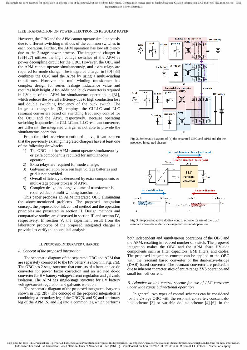
The schematic diagram of the separated OBC and APM that are separately connected to the HV battery is shown in Fig. 2(a). The OBC has 2-stage structure that consists of a front-end ac-dc converter for power factor correction and an isolated dc-dc converter for HV battery voltage/current regulation and galvanic isolation. The APM has single-stage structure for LV battery voltage/current regulation and galvanic isolation.
The schematic diagram of the proposed integrated charger is shown in Fig. 2(b). The concept of the proposed integration is combining a secondary leg of the OBC (S1 and S2) and a primary leg of the APM (S3 and S4) into a common leg which performs
both independent and simultaneous operations of the OBC and the APM, resulting in reduced number of switch. The proposed integration makes the OBC and the APM share HV-side components such as filter capacitors, EMI filters, and cables. The proposed integration concept can be applied to the OBC with the resonant based converter or the dual-active-bridge (DAB) based converter. The resonant converter are preferable due to inherent characteristics of entire range ZVS operation and small turn-off current.
B. Adaptive dc-link control scheme for use of LLC converter under wide range bidirectional operation
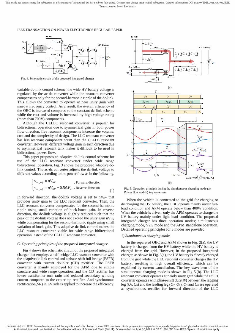
In general, two types of control schemes can be considered for the 2-stage OBC with the resonant converter; constant dc-link scheme [3] or variable dc-link scheme [4]-[6]. In the
Fig. 3. Proposed adaptive dc-link control scheme for use of the LLC resonant converter under wide range bidirectional operation
Fig. 2. Schematic diagram of (a) the separated OBC and APM and (b) the proposed integrated charger
Authorized licensed use limited to: Seoul National Univ of Science & Tech (SNUT). Downloaded on April 10,2021 at 02:51:59 UTC from IEEE Xplore. Restrictions apply.
0885-8993 (c) 2021 IEEE. Personal use is permitted, but republication/redistribution requires IEEE permission. See http://www.ieee.org/publications_standards/publications/rights/index.html for more information.
This article has been accepted for publication in a future issue of this journal, but has not been fully edited. Content may change prior to final publication. Citation information: DOI 10.1109/TPEL.2021.3063931, IEEETransactions on Power Electronics
IEEE TRANSACTION ON POWER ELECTRONICS REGULAR PAPER
variable dc-link control scheme, the wide HV battery voltage is regulated by the ac-dc converter while the resonant converter compensates only for the second-harmonic ripple of the dc-link. This allows the converter to operate at near unity gain with narrow frequency control. As a result, the overall efficiency of the OBC is increased compared to the constant dc-link scheme while the cost and volume is increased by high voltage rating (more than 700V) components.
Although the CLLLC resonant converter is popular for bidirectional operation due to symmetrical gain in both power flow direction, five resonant components increase the volume, cost and the complexity of design. The LLC resonant converter has less resonant component count than the CLLLC resonant converter. However, different voltage gain in each direction due to asymmetrical resonant tank makes it difficult to be used in bidirectional power flow.
This paper proposes an adaptive dc-link control scheme for use of the LLC resonant converter under wide range bidirectional operation. Fig. 3 shows the proposed adaptive dc- link control. The ac-dc converter adjusts the dc-link voltage to different values according to the power flow as in the following.
, Forward direction
, Reverse direction
_
_ 0.5
dc ref HV
dc ref HV dc
v nV
v nV V
= = − ∆ (1)
In forward direction, the dc-link voltage is set to nVHV that provides unity gain to the LLC resonant converter. Then, the LLC resonant converter compensates for the second-harmonic ripple using small variation of buck-boost gain. In reverse direction, the dc-link voltage is slightly reduced such that the peak of the dc-link voltage does not exceed the unity gain nVHV while compensating for the second-harmonic ripple using small variation of buck gain. This adaptive dc-link control makes the LLC resonant converter viable for wide range bidirectional operation instead of the CLLLC resonant converter.
C. Operating principles of the proposed integrated charger
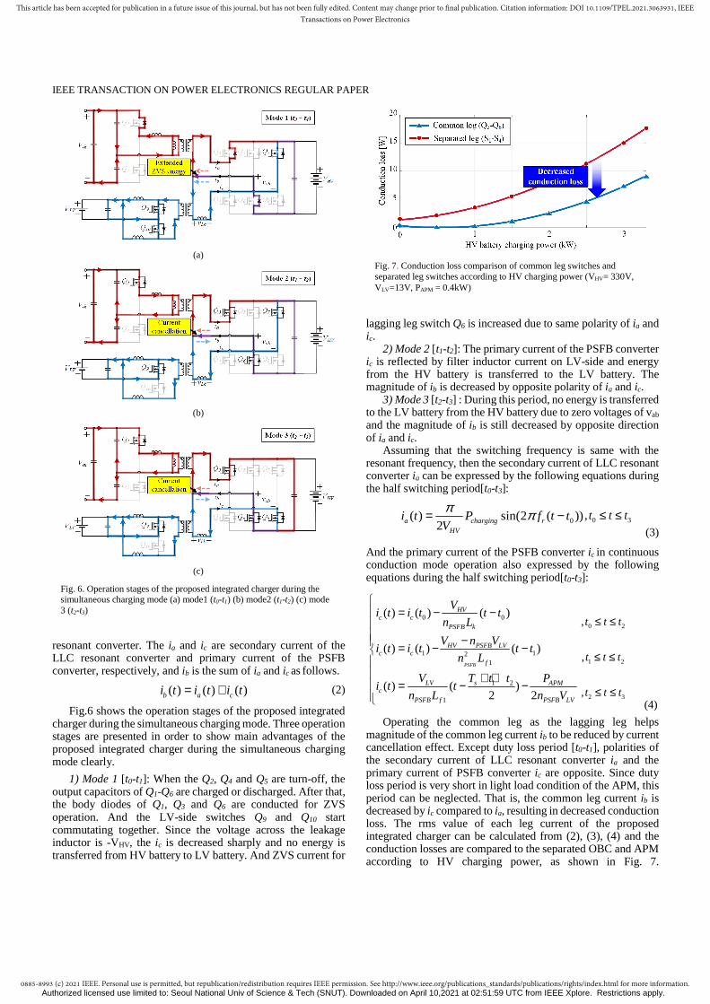
Fig 4 shows the schematic circuit of the proposed integrated charger that employs a half-bridge LLC resonant converter with the adaptive dc-link control and a phase-shift full-bridge (PSFB) converter with current doubler (CD) rectifier. The PSFB converter is mainly employed for the APM due to simple structure and wide range operation, and the CD rectifier has lower transformer turn ratio and reduced secondary winding current compared to the center-tap rectifier. And synchronous rectification(SR) in LV side is applied to increase the efficiency.
When the vehicle is connected to the grid for charging or discharging the HV battery, the OBC operate mainly under full-load condition and APM operate below than 400W condition. When the vehicle is driven, only the APM operates to charge the LV battery mainly under light load condition. The proposed integrated charger has three operation modes; simultaneous charging mode, V2G mode and the APM standalone operation. Detailed operating principles for 3 modes are provided.
1) Simultaneous charging mode
In the separated OBC and APM shown in Fig. 2(a), the LV battery is charged from the HV battery while the HV battery is charged from the grid. However, in the proposed integrated charger, as shown in Fig. 5(a), the LV battery is directly charged from the grid while the LLC resonant converter charges the HV battery, resulting in high overall efficiency, which can be explained by current cancellation. The key waveform of the simultaneous charging mode is shown in Fig 5.(b). The LLC resonant converter operates at nearly unity gain while the PSFB converter operates with phase-shift duty(Φ) between the lagging leg (Q5, Q6) and the leading leg (Q7, Q8). Q3 and Q4 are operated as synchronous rectifier for forward direction of the LLC
(a)
(b)
Fig. 5. Operation principle during the simultaneous charging mode (a) Power flow and (b) key waveform
Fig. 4. Schematic circuit of the proposed integrated charger
Authorized licensed use limited to: Seoul National Univ of Science & Tech (SNUT). Downloaded on April 10,2021 at 02:51:59 UTC from IEEE Xplore. Restrictions apply.
0885-8993 (c) 2021 IEEE. Personal use is permitted, but republication/redistribution requires IEEE permission. See http://www.ieee.org/publications_standards/publications/rights/index.html for more information.
This article has been accepted for publication in a future issue of this journal, but has not been fully edited. Content may change prior to final publication. Citation information: DOI 10.1109/TPEL.2021.3063931, IEEETransactions on Power Electronics
IEEE TRANSACTION ON POWER ELECTRONICS REGULAR PAPER
resonant converter. The ia and ic are secondary current of the LLC resonant converter and primary current of the PSFB converter, respectively, and ib is the sum of ia and ic as follows.
( ) ( ) ( )b a ci t i t i t= + (2)
Fig.6 shows the operation stages of the proposed integrated charger during the simultaneous charging mode. Three operation stages are presented in order to show main advantages of the proposed integrated charger during the simultaneous charging mode clearly.
1) Mode 1 [t0-t1]: When the Q2, Q4 and Q5 are turn-off, the output capacitors of Q1-Q6 are charged or discharged. After that, the body diodes of Q1, Q3 and Q6 are conducted for ZVS operation. And the LV-side switches Q9 and Q10 start commutating together. Since the voltage across the leakage inductor is -VHV, the ic is decreased sharply and no energy is transferred from HV battery to LV battery. And ZVS current for
lagging leg switch Q6 is increased due to same polarity of ia and ic.
2) Mode 2 [t1-t2]: The primary current of the PSFB converter ic is reflected by filter inductor current on LV-side and energy from the HV battery is transferred to the LV battery. The magnitude of ib is decreased by opposite polarity of ia and ic.
3) Mode 3 [t2-t3] : During this period, no energy is transferred to the LV battery from the HV battery due to zero voltages of vab and the magnitude of ib is still decreased by opposite direction of ia and ic.
Assuming that the switching frequency is same with the resonant frequency, then the secondary current of LLC resonant converter ia can be expressed by the following equations during the half switching period[t0-t3]:
(3)
And the primary current of the PSFB converter ic in continuous conduction mode operation also expressed by the following equations during the half switching period[t0-t3]:
0 0
1 121
1 2
1
( ) ( ) ( )
( ) ( ) ( )
( ) ( )2 2
PSFB
HVc c
PSFB k
HV PSFB LVc c
f
LV s APMc
PSFB f PSFB LV
Vi t i t t t
n L
V n Vi t i t t t
n L
V T t t Pi t t
n L n V
= − − − = − − + + = − −
0 2,t t t≤ ≤
1 2,t t t≤ ≤
2 3,t t t≤ ≤ (4)
Operating the common leg as the lagging leg helps magnitude of the common leg current ib to be reduced by current cancellation effect. Except duty loss period [t0-t1], polarities of the secondary current of LLC resonant converter ia and the primary current of PSFB converter ic are opposite. Since duty loss period is very short in light load condition of the APM, this period can be neglected. That is, the common leg current ib is decreased by ic compared to ia, resulting in decreased conduction loss. The rms value of each leg current of the proposed integrated charger can be calculated from (2), (3), (4) and the conduction losses are compared to the separated OBC and APM according to HV charging power, as shown in Fig. 7.
0 3,t t t≤ ≤0( ) sin(2 ( ))2a charging r
HV
i t P f t tV
π π= −
Fig. 7. Conduction loss comparison of common leg switches and separated leg switches according to HV charging power (VHV= 330V, VLV=13V, PAPM = 0.4kW)
(a)
(b)
(c)
Fig. 6. Operation stages of the proposed integrated charger during the simultaneous charging mode (a) mode1 (t0-t1) (b) mode2 (t1-t2) (c) mode 3 (t2-t3)
Authorized licensed use limited to: Seoul National Univ of Science & Tech (SNUT). Downloaded on April 10,2021 at 02:51:59 UTC from IEEE Xplore. Restrictions apply.
0885-8993 (c) 2021 IEEE. Personal use is permitted, but republication/redistribution requires IEEE permission. See http://www.ieee.org/publications_standards/publications/rights/index.html for more information.
This article has been accepted for publication in a future issue of this journal, but has not been fully edited. Content may change prior to final publication. Citation information: DOI 10.1109/TPEL.2021.3063931, IEEETransactions on Power Electronics
IEEE TRANSACTION ON POWER ELECTRONICS REGULAR PAPER
Conduction loss of four switches (S1-S4) of the separated charger in Fig 2.(a) is higher than that of the common leg switches of the proposed integrated charger under entire load range. It is noted that the proposed integrated charger not only reduces the number of switches but also has lower conduction loss due to the current cancellation effect compared to the separated OBC and APM.
In the conventional PSFB converter, ZVS energy of the lagging leg switch may not be sufficient to achieve ZVS operation under light load condition. ZVS operation even under light load condition is important since the APM usually operates under 400W in the simultaneous operation. The proposed integrated charger can extend ZVS range of the lagging leg by operating the common leg as the lagging leg of the PSFB converter. That is, as shown in Fig. 5(b), the ZVS energy of the lagging leg switches of the proposed integrated charger Ecommon during the dead-time period [t3-t4] is increased by ZVS energy of the LLC resonant converter ELLC.
Three HV-side legs operate as two independent full-bridges for OBC and APM; full bridge switches for OBC are Q3-Q6 and full-bridge switches for APM are Q5-Q8. That is, two batteries are independently regulated by different control variables. And ia and ic is determined by the HV battery current and LV battery
current, respectively, which means that sudden load change on one terminal does not affect to the other terminal.
2) V2G mode
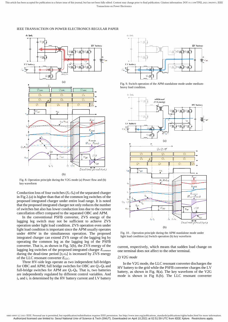
In the V2G mode, the LLC resonant converter discharges the HV battery to the grid while the PSFB converter charges the LV battery, as shown in Fig. 8(a). The key waveform of the V2G mode is shown in Fig 8.(b). The LLC resonant converter
(a)
(b)
Fig. 8. Operation principle during the V2G mode (a) Power flow and (b) key waveform
(a)
(b)
Fig. 10. . Operation principle during the APM standalone mode under light load condition (a) Switch operation (b) key waveform
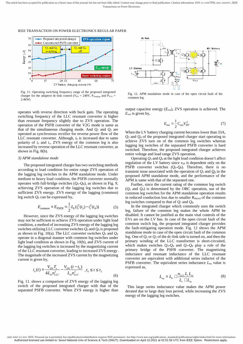
Fig. 9. Switch operation of the APM standalone mode under medium-heavy load condition.
Authorized licensed use limited to: Seoul National Univ of Science & Tech (SNUT). Downloaded on April 10,2021 at 02:51:59 UTC from IEEE Xplore. Restrictions apply.
0885-8993 (c) 2021 IEEE. Personal use is permitted, but republication/redistribution requires IEEE permission. See http://www.ieee.org/publications_standards/publications/rights/index.html for more information.
This article has been accepted for publication in a future issue of this journal, but has not been fully edited. Content may change prior to final publication. Citation information: DOI 10.1109/TPEL.2021.3063931, IEEETransactions on Power Electronics
IEEE TRANSACTION ON POWER ELECTRONICS REGULAR PAPER
operates with reverse direction with buck gain. The operating switching frequency of the LLC resonant converter is higher than resonant frequency slightly due to ZVS operation. The operation of the PSFB converter of the V2G mode is same as that of the simultaneous charging mode. And Q1 and Q2 are operated as synchronous rectifier for reverse power flow of the LLC resonant converter. Although, ib is increased due to same polarity of ia and ic, ZVS energy of the common leg is also increased by reverse operation of the LLC resonant converter, as shown in Fig. 8(b).
3) APM standalone mode
The proposed integrated charger has two switching methods according to load condition for entire range ZVS operation of the lagging leg switches in the APM standalone mode. Under medium to heavy load condition, the PSFB converter normally operates with full-bridge switches (Q5-Q8), as shown in Fig. 9, achieving ZVS operation of the lagging leg switches due to sufficient ZVS energy. ZVS energy of the lagging (common) leg switch Q5 can be expressed by,
2 23 4
1( ( ) ( ))
2common PSFB k c cE E L i t i t= = − (5)
However, since the ZVS energy of the lagging leg switches may not be sufficient to achieve ZVS operation under light load condition, a method of increasing ZVS energy of the lagging leg switches utilizing LLC converter switches Q3 and Q4 is proposed as shown in Fig. 10(a). The LLC converter switches Q3 and Q4 operate in a diagonal manner with common leg switches under light load condition as shown in Fig. 10(b), and ZVS current of the lagging leg switches is increased by the magnetizing current of the LLC resonant converter, leading to increased ZVS energy . The magnitude of the increased ZVS current by the magnetizing current is given by,
02 2
( )( )
4HV s HV
am LLC m LLC
V T V t ti t
L n L n
−= − 0 3,t t t≤ ≤ (6)
Fig. 11. shows a comparison of ZVS energy of the lagging leg switch of the proposed integrated charger with that of the separated PSFB converter. When ZVS energy is higher than
output capacitor energy (Eoss), ZVS operation is achieved. The Eoss is given by,
21
2oss oss HVE C V= (7)
When the LV battery charging current becomes lower than 33A, Q3 and Q4 of the proposed integrated charger start operating to achieve ZVS turn on of the common leg switches whereas lagging leg switches of the separated PSFB converter is hard switched. Therefore, the proposed integrated charger achieves entire voltage and load range ZVS operation. Operating Q3 and Q4 at the light load condition doesn’t affect regulation of the LV battery since vab is dependent only on the PSFB converter switches (Q5-Q8). Therefore, there is no transient issue associated with the operation of Q3 and Q4 in the proposed APM standalone mode, and the performance of the APM is same with that of the separated one.
Further, since the current rating of the common leg switch (Q5 and Q6) is determined by the OBC operation, use of the common leg switches for the APM standalone operation results in reduced conduction loss due to smaller Rds(on) of the common leg switches compared to that of Q7 and Q8.
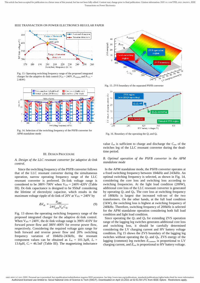
In the integrated charger which commonly uses the switch leg, failure of the common leg makes the whole APM be disabled. It cannot be justified as the main vital controls of the EVs are on the LV bus. In case of the open circuit fault of the common switch leg, the proposed integrated charger provides the fault-mitigating operation mode. Fig. 12 shows the APM standalone mode in case of the open circuit fault of the common leg. One of Q1 or Q2 of the dc-link side is turned on, and then the primary winding of the LLC transformer is short-circuited, which makes switches Q3-Q4 and Q7-Q8 play a role of the primary bridge of the PSFB converter. The magnetizing inductance and resonant inductance of the LLC resonant converter are equivalent with additional series inductor of the PSFB converter. The equivalent series inductance Leq value is expressed as,
LLC r meq k
r m
n L LL L
L L= +
+ (8)
This large series inductance value makes the APM power derated due to large duty loss period, while increasing the ZVS energy of the lagging leg switches.
Fig. 12. APM standalone mode in case of the open circuit fault of the common leg.
Fig. 11. Operating switching frequency range of the proposed integrated charger for the adaptive dc-link control (VHV = 240V, Pcharging and PV2G = 2.4kW)
Authorized licensed use limited to: Seoul National Univ of Science & Tech (SNUT). Downloaded on April 10,2021 at 02:51:59 UTC from IEEE Xplore. Restrictions apply.
0885-8993 (c) 2021 IEEE. Personal use is permitted, but republication/redistribution requires IEEE permission. See http://www.ieee.org/publications_standards/publications/rights/index.html for more information.
This article has been accepted for publication in a future issue of this journal, but has not been fully edited. Content may change prior to final publication. Citation information: DOI 10.1109/TPEL.2021.3063931, IEEETransactions on Power Electronics
IEEE TRANSACTION ON POWER ELECTRONICS REGULAR PAPER
III. DESIGN PROCEDURE
A. Design of the LLC resonant converter for adaptive dc-link control.
Since the switching frequency of the PSFB converter follows that of the LLC resonant converter during the simultaneous operation, narrow operating frequency range of the LLC resonant converter is preferred. Dc-link voltage range is considered to be 380V-700V when VHV = 240V-420V (Table III). Dc-link capacitance is designed to be 950uF considering the lifetime of electrolytic capacitor, which results in the maximum voltage ripple of dc-link of 20V at VHV = 240V by
2
OBCdc
grid dc dc
PV
f V Cπ∆ = (9)
Fig. 13 shows the operating switching frequency range of the proposed integrated charger for the adaptive dc-link control. When VHV = 240V, the dc-link voltage range is 390V-410V for forward power flow and 380V-400V for reverse power flow, respectively. Considering the required voltage gain range for both forward and reverse power flow and 20% switching frequency variation of 184kHz-243kHz, the resonant component values can be obtained as Lm = 101.3μH, Lr = 13.6μH, Cr = 46.5nF (Table III). The magnetizing inductance
value Lm is sufficient to charge and discharge the Coss of the switches leg of the LLC resonant converter during the dead-time period.
B. Optimal operation of the PSFB converter in the APM standalone mode
In the APM standalone mode, the PSFB converter operates at a fixed switching frequency between 184kHz and 243kHz. An optimal switching frequency is selected, as shown in Fig. 14, considering the core loss and switching loss according to switching frequencies. At the light load condition (200W), additional core loss of the LLC resonant converter is generated by operating Q3 and Q4. The core loss at switching frequency of 180kHz is largest due increased volt-sec of the two transformers. On the other hands, at the full load condition (1kW), the switching loss is highest at switching frequency of 240kHz. Therefore, switching frequency of 200kHz is selected for the APM standalone operation considering both full load condition and light load condition. Since operating the Q3 and Q4 for extending ZVS operation
range of the lagging leg switches generates additional core loss and switching loss, it should be carefully determined considering the LV charging current and HV battery voltage condition. Fig 15 shows the ZVS boundary of the lagging leg switches without operating the Q3 and Q4. ZVS energy of the lagging (common) leg switches Ecommon is proportional to LV charging current, and Eoss is proportional to HV battery voltage.
Fig. 14. Selection of the switching frequency of the PSFB converter for APM standalone mode
Fig. 15. ZVS boundary of the separated PSFB converter
Fig. 13. Operating switching frequency range of the proposed integrated charger for the adaptive dc-link control (VHV = 240V, Pcharging and PV2G = 2.4kW)
Fig. 16. Boundary of the operating the Q3 and Q4
Authorized licensed use limited to: Seoul National Univ of Science & Tech (SNUT). Downloaded on April 10,2021 at 02:51:59 UTC from IEEE Xplore. Restrictions apply.
0885-8993 (c) 2021 IEEE. Personal use is permitted, but republication/redistribution requires IEEE permission. See http://www.ieee.org/publications_standards/publications/rights/index.html for more information.
This article has been accepted for publication in a future issue of this journal, but has not been fully edited. Content may change prior to final publication. Citation information: DOI 10.1109/TPEL.2021.3063931, IEEETransactions on Power Electronics
IEEE TRANSACTION ON POWER ELECTRONICS REGULAR PAPER
The ZVS boundary can be obtained with Ecommon = Eoss. Fig. 16 shows the boundary of the operating the Q3 and Q4 considering ZVS boundary of lagging leg switches. Q3 and Q4 operate when ZVS energy of the lagging leg switches is lower than Eoss. Therefore, entire range ZVS operation of the lagging leg switches can be achieved by operating Q3 and Q4 based on the operation boundary that is the same as ZVS boundary in Fig. 15.
IV. COMPARATIVE STUDIES
In order to show the effectiveness of the proposed integrated charger, the proposed integrated charger is compared with the separated OBC and APM in Fig. 2(a) in terms of cost, volume and efficiency. Fig. 17(a) and (b) show volume and cost
comparisons. Overall volume and cost of the proposed integrated charger are decreased by 17% and 19%, respectively, due to reduced switches count and shared input filter. The efficiency of the proposed integrated charger is shown to be higher at both simultaneous mode and APM standalone mode (see fig. 21 and fig. 25). Table II shows the comparison of the proposed integrated
charger to existing integrated chargers [24]-[25], [31]-[32]. The proposed integrated charger provides low profile due to use of two small transformers compared to the transformer integration method using a three-winding transformer [31]-[32]. The proposed integrated charger does not necessitate extra relay for integration and additional circuit for simultaneous operation
TABLE III SYSTEM SPECIFICATIONS OF THE PROPOSED INTEGRATED CHARGER
(VHV:240V-420V, VLV :11-14V)
Operation condition
Parameter Value (unit)
Simultaneous Mode
HV battery charging power (Pcharging) /discharging power (PV2G)
3.3kW
LV battery charging power (PAPM) 0.4kW
Maximum HV battery current 10A
Maximum LV battery current 30A
DC link voltage (Vdc) 380V-700V
APM Standalone Mode
LV battery charging power (PAPM) 1kW
Maximum LV battery current 74A
TABLE II KEY PARAMETERS OF THE PROPOSED INTEGRATED CHARGER
Parameters Symbol Values
LLC resonant converter
Dc-link side switches Q1, Q2 900V, 65mΩ HV-side switches Q3, Q4 650V, 80mΩ Magnetizing inductance Lm 101.3μH Resonant inductance Lr 13.6μH Resonant capacitance Cr 46.5nF Resonant frequency fr 200kHz Transformer turn ratio nLLC 1.2 Dc-link side filter capacitance Cdc 950μF HV battery-side filter capacitance CHV 20μF
PSFB converter
HV-side switches Q7, Q8 650V, 120mΩ LV-side switches Q9, Q10 100V, 1.5mΩ Leakage inductance Lk 3.8μH Filter inductance Lf1, Lf2 2.7μH Transformer turn ratio nPSFB 6.5 LV battery-side filter capacitance Clv 66μF
Common leg switches Q5, Q6 650V, 80mΩ Switching frequency fsw 184kHz~243kHz
TABLE I COMPARISON WITH THE EXISTING INTEGRATED CHARGER
Topology (OBC, APM)
Proposed [24] [25] [31] [32] LLC, PSFB DAB, DAB+buck buck-boost , LLC PSFB, PSFB CLLC, LLC
Galvanic isolation O X X O O Key integration components switches switches switches transformer transformer
Number of relay for integration 0 1 1 1 1 Simultaneous operation O X O (with extra circuit) O (with extra circuit) X Entire load ZVS range O X X X O
(a) (b)
Fig. 17. (a) Volume and (b) cost comparison of the proposed integrated charger and the separated charger
Fig. 18. Prototype of the proposed integrated charger
Authorized licensed use limited to: Seoul National Univ of Science & Tech (SNUT). Downloaded on April 10,2021 at 02:51:59 UTC from IEEE Xplore. Restrictions apply.
0885-8993 (c) 2021 IEEE. Personal use is permitted, but republication/redistribution requires IEEE permission. See http://www.ieee.org/publications_standards/publications/rights/index.html for more information.
This article has been accepted for publication in a future issue of this journal, but has not been fully edited. Content may change prior to final publication. Citation information: DOI 10.1109/TPEL.2021.3063931, IEEETransactions on Power Electronics
IEEE TRANSACTION ON POWER ELECTRONICS REGULAR PAPER
unlikely the existing integrated chargers. In addition, the proposed integrated charger achieves entire ZVS range of all switches of the PSFB converter in both simultaneous charging/V2G mode and the APM standalone operation modes. If the common leg fails, the whole APM is disabled in the existing integrated charger. However, the proposed integrated charger can deliver the partial power to the LV battery, while achieving ZVS operation of the lagging leg switches. Therefore, the proposed integrated charger clearly stands out from not only the separated OBC and APM but also the existing integrated chargers.
V. EXPERIMENT RESULT
In order to verify the performance of the proposed integrated charger, a laboratory prototype integrating 3.7kW LLC resonant converter and 1kW PSFB converter is built on a PCB board, as illustrated in Fig 18. The LLC resonant converter and the PSFB converter share the heats ink, HV battery-side filters and sensors. The key parameters and system specifications of the proposed integrated charger are summarized in Table II and Table III respectively. The dc-link side and HV-side switches were implemented using SiC devices (Q1,Q2 : E3M0065090D from Cree, Q3~Q6 : SCT3080AL from Rohm, Q7, Q8 : SCT3120AL from Rohm) and LV side switches were implemented using Si device (Q9, Q10 : IAUT300N10S5N015 from Infineon). The transformer and filter inductor were implemented with PL15
(a)
(b)
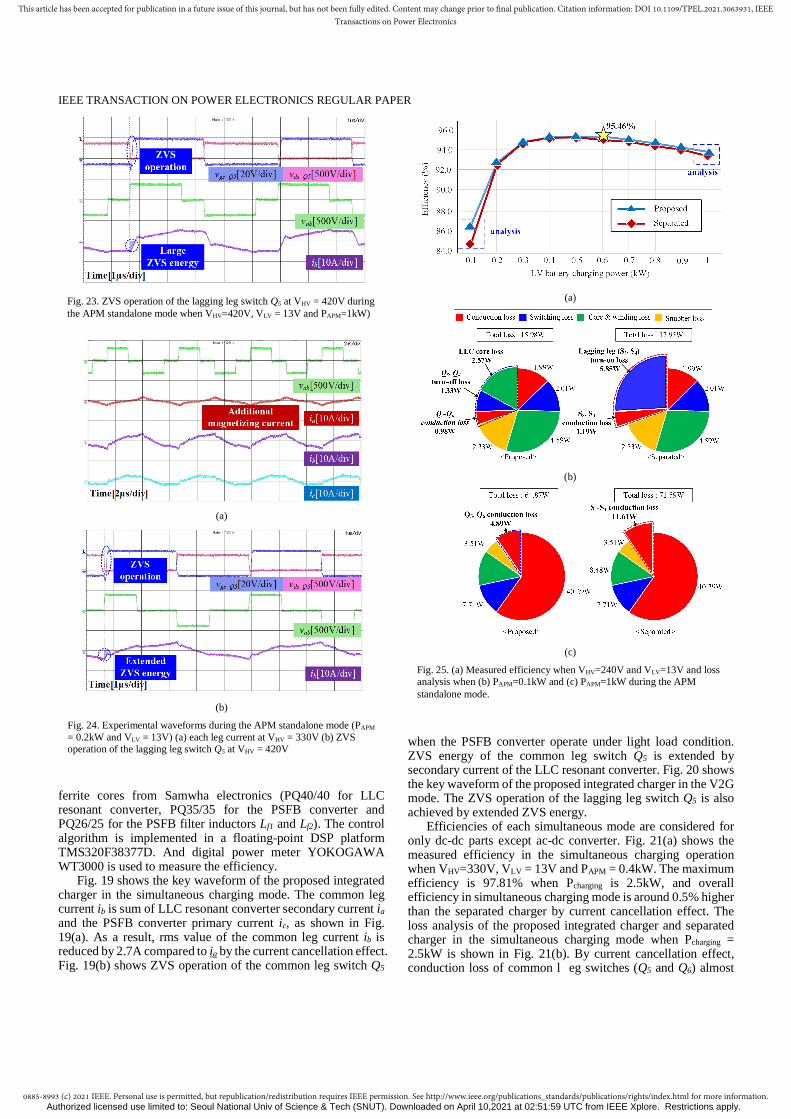
Fig. 21. (a) Measured efficiency when VHV=330V, VLV=13V and PAPM= 0.4kW and (b) loss analysis when Pcharging=2.5kW during the simultaneous charging mode.
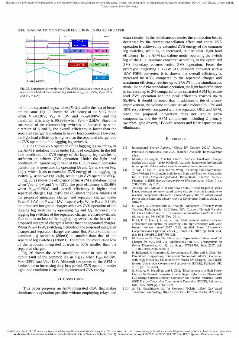
Fig. 20. ZVS operation of the lagging leg switch Q5 at VHV = 420V during the V2G mode (PV2G = 3.3kW, PAPM = 0.4kW and VLV = 13V)
Fig. 22. Measured efficiency during the V2G mode when VHV=330V, VLV= 13V and PAPM=0.2kW.
(a)
(b)
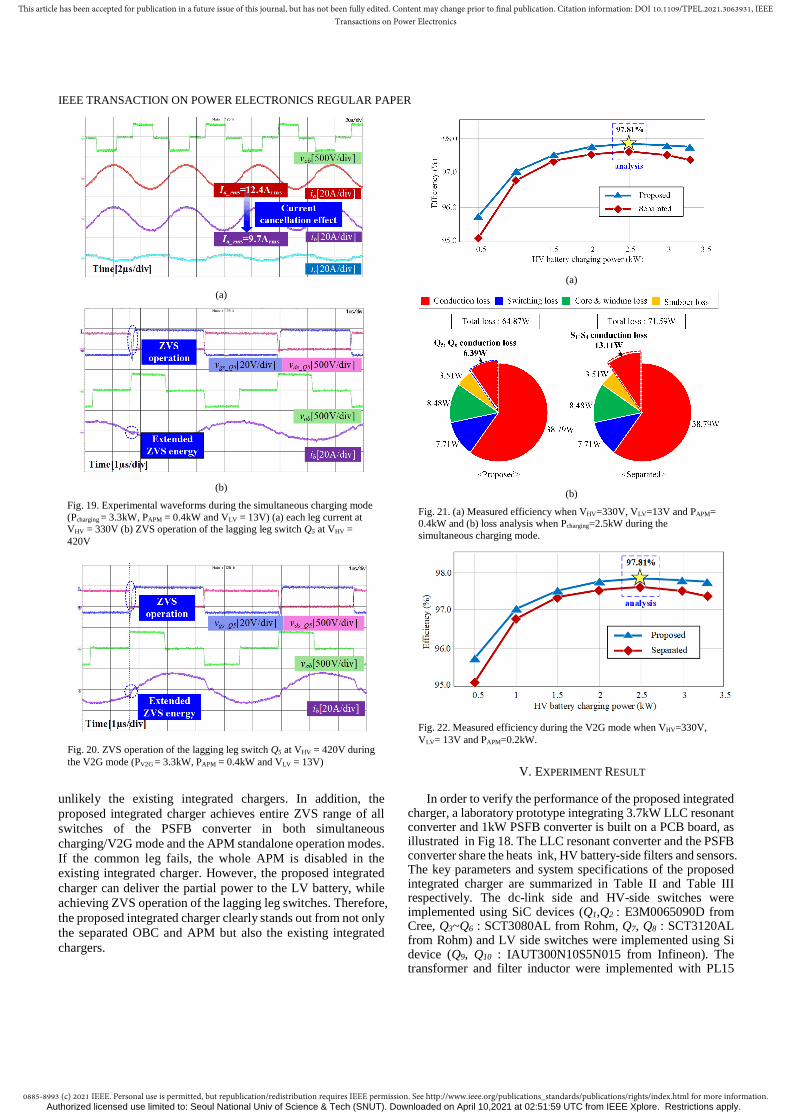
Fig. 19. Experimental waveforms during the simultaneous charging mode (Pcharging = 3.3kW, PAPM = 0.4kW and VLV = 13V) (a) each leg current at VHV = 330V (b) ZVS operation of the lagging leg switch Q5 at VHV = 420V
Authorized licensed use limited to: Seoul National Univ of Science & Tech (SNUT). Downloaded on April 10,2021 at 02:51:59 UTC from IEEE Xplore. Restrictions apply.
0885-8993 (c) 2021 IEEE. Personal use is permitted, but republication/redistribution requires IEEE permission. See http://www.ieee.org/publications_standards/publications/rights/index.html for more information.
This article has been accepted for publication in a future issue of this journal, but has not been fully edited. Content may change prior to final publication. Citation information: DOI 10.1109/TPEL.2021.3063931, IEEETransactions on Power Electronics
IEEE TRANSACTION ON POWER ELECTRONICS REGULAR PAPER
ferrite cores from Samwha electronics (PQ40/40 for LLC resonant converter, PQ35/35 for the PSFB converter and PQ26/25 for the PSFB filter inductors Lf1 and Lf2). The control algorithm is implemented in a floating-point DSP platform TMS320F38377D. And digital power meter YOKOGAWA WT3000 is used to measure the efficiency.
Fig. 19 shows the key waveform of the proposed integrated charger in the simultaneous charging mode. The common leg current ib is sum of LLC resonant converter secondary current ia and the PSFB converter primary current ic, as shown in Fig. 19(a). As a result, rms value of the common leg current ib is reduced by 2.7A compared to ia by the current cancellation effect. Fig. 19(b) shows ZVS operation of the common leg switch Q5
when the PSFB converter operate under light load condition. ZVS energy of the common leg switch Q5 is extended by secondary current of the LLC resonant converter. Fig. 20 shows the key waveform of the proposed integrated charger in the V2G mode. The ZVS operation of the lagging leg switch Q5 is also achieved by extended ZVS energy. Efficiencies of each simultaneous mode are considered for only dc-dc parts except ac-dc converter. Fig. 21(a) shows the measured efficiency in the simultaneous charging operation when VHV=330V, VLV = 13V and PAPM = 0.4kW. The maximum efficiency is 97.81% when Pcharging is 2.5kW, and overall efficiency in simultaneous charging mode is around 0.5% higher than the separated charger by current cancellation effect. The loss analysis of the proposed integrated charger and separated charger in the simultaneous charging mode when Pcharging = 2.5kW is shown in Fig. 21(b). By current cancellation effect, conduction loss of common l eg switches (Q5 and Q6) almost
Fig. 23. ZVS operation of the lagging leg switch Q5 at VHV = 420V during the APM standalone mode when VHV=420V, VLV = 13V and PAPM=1kW)
(a)
(b)
(c)
Fig. 25. (a) Measured efficiency when VHV=240V and VLV=13V and loss analysis when (b) PAPM=0.1kW and (c) PAPM=1kW during the APM standalone mode.
(a)
(b)
Fig. 24. Experimental waveforms during the APM standalone mode (PAPM = 0.2kW and VLV = 13V) (a) each leg current at VHV = 330V (b) ZVS operation of the lagging leg switch Q5 at VHV = 420V
Authorized licensed use limited to: Seoul National Univ of Science & Tech (SNUT). Downloaded on April 10,2021 at 02:51:59 UTC from IEEE Xplore. Restrictions apply.
0885-8993 (c) 2021 IEEE. Personal use is permitted, but republication/redistribution requires IEEE permission. See http://www.ieee.org/publications_standards/publications/rights/index.html for more information.
This article has been accepted for publication in a future issue of this journal, but has not been fully edited. Content may change prior to final publication. Citation information: DOI 10.1109/TPEL.2021.3063931, IEEETransactions on Power Electronics
IEEE TRANSACTION ON POWER ELECTRONICS REGULAR PAPER
half of the separated leg switches (S1-S4), while the rest of losses are the same. Fig. 22 shows the efficiency of the V2G mode when VHV=330V, VLV = 13V and PAPM=200W, and the maximum efficiency is 96.89% when PV2G = 2.5kW. Since the rms value of the common leg switches is increased by same direction of ia and ic, the overall efficiency is lower than the separated charger at medium to heavy load condition. However, the light load efficiency is higher than the separated charger due to ZVS operation of the lagging leg switches. Fig. 23 shows ZVS operation of the lagging leg switch Q5 in the APM standalone mode under full load condition. In the full load condition, the ZVS energy of the lagging leg switches is sufficient to achieve ZVS operation. Under the light load condition, m agnetizing current of the LLC resonant converter transformer is generated by operating Q3 and Q4, as shown Fig. 24(a), which leads to extended ZVS energy of the lagging leg switch Q5, as shown Fig. 24(b), resulting in ZVS operation of Q5.
Fig. 25(a) shows the efficiency of the APM standalone mode when VHV=240V and VLV=13V. The peak efficiency is 95.46% when PAPM=0.6kW, and overall efficiency is higher than separated charger. Fig. 25(b) and (c) shows the loss analysis of the proposed integrated charger and separated charger under PAPM=0.1kW and PAPM=1kW, respectively. When PAPM=0.1kW, the proposed integrated charger achieves ZVS operation of the lagging leg switches by operating Q3 and Q4. However, the lagging leg switches of the separated charger are hard-switched. Due to turn on loss of the lagging leg switches, the loss of the proposed integrated charger is lower than the separated charger. When PAPM=1kW, switching methods of the proposed integrated charger and separated charger are same. But, Rds(on) value of the common leg switches (80mΩ) is smaller than that of the separated leg switches (120mΩ). Therefore, the conduction loss of the proposed integrated charger is 66% smaller than the separated charger.
Fig. 26 shows the APM standalone mode in case of open circuit fault of the common leg in Fig.12 when PAPM=200W, VHV=330V and VLV=13V. Although the power of the APM is limited due to increasing duty-loss period, ZVS operation under light load condition is ensured by increased ZVS energy.
VI. CONCLUSION
This paper proposes an APM integrated OBC that makes simultaneous operation possible without employing relays and
extra circuits. In the simultaneous mode, the conduction loss is decreased by the current cancellation effect and entire ZVS operation is achieved by extended ZVS energy of the common leg switches, resulting in increased, in particular, light load efficiency. In the APM standalone mode, operating the switch leg of the LLC resonant converter according to the optimized ZVS boundary ensures entire ZVS operation. From the prototype integrating a 3.7kW LLC resonant converter with a 1kW PSFB converter, it is shown that overall efficiency is increased by 0.5% compared to the separated charger and maximum efficiency reaches up to 97.61% in the simultaneous mode. In the APM standalone operation, the light load efficiency is increased up to 2% compared to the separated APM by entire load ZVS operation and the peak efficiency reaches up to 95.46%. It should be noted that in addition to the efficiency improvement, the volume and cost are also reduced by 17% and 19%, respectively, compared with the separated OBC and APM, since the proposed integration does not require extra components, and the APM components including 2 primary switches, gate drivers, HV-side sensors and filter capacitor are eliminated.
REFERENCES
[1] International Energy Agency, “Global EV Outlook 2020,” France, Paris:IEA Publications, June 2020. [Online]. Available: https://webstor e.iea.
[2] Mobility Foresights, “Global Electric Vehicle On-Board Charger Market 2019-2025,” 2019. [Online]. Available: https://mobilityforesigh ts.com/product/global-electric-vehicle-on-board-charger-market/
[3] Y. Yan, H. Bai, A. Foote and W. Wang, "Securing Full-Power-Range Zero-Voltage Switching in Both Steady-State and Transient Operations for a Dual-Active-Bridge-Based Bidirectional Electric Vehicle Charger," in IEEE Transactions on Power Electronics, vol. 35, no. 7, pp. 7506-7519, July 2020..
[4] Junsung Park, Minjae Kim and Sewan Choi, "Fixed frequency series loaded resonant converter based battery charger which is insensitive to resonant component tolerances," Proceedings of The 7th International Power Electronics and Motion Control Conference, Harbin, 2012, pp. 918-922,
[5] H. Wang, S. Dusmez and A. Khaligh, "Maximum Efficiency Point Tracking Technique for LLC-Based PEV Chargers Through Variable DC Link Control," in IEEE Transactions on Industrial Electronics, vol. 61, no. 11, pp. 6041-6049, Nov. 2014.
[6] B. Li, F. C. Lee, Q. Li and Z. Liu, "Bi-directional on-board charger architecture and control for achieving ultra-high efficiency with wide battery voltage range," 2017 IEEE Applied Power Electronics Conference and Exposition (APEC), Tampa, FL, 2017, pp. 3688-3694, doi: 10.1109/APEC.2017.7931228.
[7] M. Kwon and S. Choi, "An Electrolytic Capacitorless Bidirectional EV Charger for V2G and V2H Applications," in IEEE Transactions on Power Electronics, vol. 32, no. 9, pp. 6792-6799, Sept. 2017, doi: 10.1109/TPEL.2016.2630711.
[8] H. Belkamel, K. Hyungjin, K. Beywongwoo, Y. Shin and S. Choi, "Bi-Directional Single-Stage Interleaved Totem-Pole AC-DC Converter with High Frequency Isolation for On-Board EV Charger," 2018 IEEE Energy Conversion Congress and Exposition (ECCE), Portland, OR, 2018, pp. 6721-6724,
[9] S. Kim, A. M. Naradhipa and S. Choi, "Development of a High Power Density GaN-based Transistor Low-Voltage High-Current Phase-Shift Full-Bridge Current Doubler Converter for Electric Vehicles," 2019 IEEE Energy Conversion Congress and Exposition (ECCE), Baltimore, MD, USA, 2019, pp. 1364-1369
[10] A. M. Naradhipa et al., "A Compact 700kHz 1.8kW GaN-based Transistor Low Voltage High Current DC-DC Converter for xEV using
Fig. 26. Experimental waveforms of the APM standalone mode in case of open circuit fault of the common leg switches (PAPM = 0.2kW, VHV=330V and VLV = 15V)
Authorized licensed use limited to: Seoul National Univ of Science & Tech (SNUT). Downloaded on April 10,2021 at 02:51:59 UTC from IEEE Xplore. Restrictions apply.

0885-8993 (c) 2021 IEEE. Personal use is permitted, but republication/redistribution requires IEEE permission. See http://www.ieee.org/publications_standards/publications/rights/index.html for more information.
This article has been accepted for publication in a future issue of this journal, but has not been fully edited. Content may change prior to final publication. Citation information: DOI 10.1109/TPEL.2021.3063931, IEEETransactions on Power Electronics
IEEE TRANSACTION ON POWER ELECTRONICS REGULAR PAPER
Planar Matrix Transformer," 2019 10th International Conference on Power Electronics and ECCE Asia (ICPE 2019 - ECCE Asia), Busan, Korea (South), 2019, pp. 1-6.
[11] B. Kim, K. Kim and S. Choi, "A 800V/14V Soft-switched Converter with Low-Voltage Rating of Switch for xEV applications," 2018 International Power Electronics Conference (IPEC-Niigata 2018 -ECCE Asia), Niigata, 2018, pp. 256-260.
[12] F. Krismer and J. W. Kolar, "Efficiency-Optimized High-Current Dual Active Bridge Converter for Automotive Applications," in IEEE Transactions on Industrial Electronics, vol. 59, no. 7, pp. 2745-2760, July 2012.
[13] G. Yang, P. Dubus and D. Sadarnac, "Double-Phase High-Efficiency, Wide Load Range High- Voltage/Low-Voltage LLC DC/DC Converter for Electric/Hybrid Vehicles," in IEEE Transactions on Power Electronics, vol. 30, no. 4, pp. 1876-1886, April 2015.
[14] Khasawneh, B., Sabra, M., and Zohdy, M., "Novel Operating Mode for DC-to-DC Converters in PHEVs," SAE Technical Paper 2013-01-1761, 2013.
[15] A. Khaligh and M. D'Antonio, "Global Trends in High-Power On-Board Chargers for Electric Vehicles," in IEEE Transactions on Vehicular Technology, vol. 68, no. 4, pp. 3306-3324, April 2019
[16] J. A. Baxter, D. A. Merced, D. J. Costinett, L. M. Tolbert and B. Ozpineci, "Review of Electrical Architectures and Power Requirements for Automated Vehicles," 2018 IEEE Transportation Electrification Conference and Expo (ITEC), Long Beach, CA, 2018
[17] U.S. DRIVE Department of Energy, “Electrical and electronics technical team roadmap,” Oct. 2017. [Online]. Available: https:// www.energy.gov/sites/prod/files/2017/11/f39/EETT%20Roadmap%2010-27-17.pdf
[18] I. Subotic, N. Bodo, E. Levi, B. Dumnic, D. Milicevic and V. Katic, "Overview of fast on-board integrated battery chargers for electric vehicles based on multiphase machines and power electronics," in IET Electric Power Applications, vol. 10, no. 3, pp. 217-229, 3 2016
[19] C. Shi and A. Khaligh, "A Two-Stage Three-Phase Integrated Charger for Electric Vehicles With Dual Cascaded Control Strategy," in IEEE Journal of Emerging and Selected Topics in Power Electronics, vol. 6, no. 2, pp. 898-909, June 2018
[20] N. Sakr, D. Sadarnac and A. Gascher, "A new combined bidirectional boost converter and battery charger for electric vehicles," IECON 2015 - 41st Annual Conference of the IEEE Industrial Electronics Society, Yokohama, 2015
[21] Y. Lee, A. Khaligh and A. Emadi, "Advanced Integrated Bidirectional AC/DC and DC/DC Converter for Plug-In Hybrid Electric Vehicles," in IEEE Transactions on Vehicular Technology, vol. 58, no. 8, pp. 3970-3980, Oct. 2009
[22] BorgWarner, “OBC + APM package integrated charger,” 2019. [Online]. Available:https://www.borgwarner.com/newsroom/press-releases/2019 /05/16/class-leading-onboard-battery-charger-strengthens-borgwarner-s-ev-systems-leadership
[23] J. G. Pinto, V. Monteiro, H. Gonçalves and J. L. Afonso, "Onboard Reconfigurable Battery Charger for Electric Vehicles With Traction-to-Auxiliary Mode," in IEEE Transactions on Vehicular Technology, vol. 63, no. 3, pp. 1104-1116, March 2014.
[24] S. Kim and F. Kang, "Multifunctional Onboard Battery Charger for Plug-in Electric Vehicles," in IEEE Transactions on Industrial Electronics, vol. 62, no. 6, pp. 3460-3472, June 2015,
[25] D. Kim, M. Kim and B. Lee, "An Integrated Battery Charger With High Power Density and Efficiency for Electric Vehicles," in IEEE Transactions on Power Electronics, vol. 32, no. 6, pp. 4553-4565, June 2017.
[26] H. V. Nguyen, D. To and D. Lee, "Onboard Battery Chargers for Plug-in Electric Vehicles With Dual Functional Circuit for Low-Voltage Battery Charging and Active Power Decoupling," in IEEE Access, vol. 6, pp. 70212-70222, 2018.
[27] R. Hou and A. Emadi, "A Primary Full-Integrated Active Filter Auxiliary Power Module in Electrified Vehicles With Single-Phase Onboard Chargers," in IEEE Transactions on Power Electronics, vol. 32, no. 11, pp. 8393-8405, Nov. 2017.
[28] I. Aghabali, J. Bauman and A. Emadi, "Analysis of Auxiliary Power Unit and Charging for an 800V Electric Vehicle," 2019 IEEE Transportation Electrification Conference and Expo (ITEC), Detroit, MI, USA, 2019, pp. 1-6.
[29] C. Liu et al., "High-Efficiency Hybrid Full-Bridge–Half-Bridge Converter With Shared ZVS Lagging Leg and Dual Outputs in Series," in IEEE Transactions on Power Electronics, vol. 28, no. 2, pp. 849-861, Feb. 2013.
[30] H. Ma, Y. Tan, L. Du, X. Han and J. Ji, "An integrated design of power converters for electric vehicles," 2017 IEEE 26th International Symposium on Industrial Electronics (ISIE), Edinburgh, 2017, pp. 600-605.
[31] Y. Kim, C. Oh, W. Sung and B. K. Lee, "Topology and Control Scheme of OBC–LDC Integrated Power Unit for Electric Vehicles," in IEEE Transactions on Power Electronics, vol. 32, no. 3, pp. 1731-1743, March 2017.
[32] Y. Tang, J. Lu, B. Wu, S. Zou, W. Ding and A. Khaligh, "An Integrated Dual-Output Isolated Converter for Plug-in Electric Vehicles," in IEEE Transactions on Vehicular Technology, vol. 67, no. 2, pp. 966-976, Feb. 2018.
[33] G. Su and L. Tang, "A new integrated onboard charger and accessory power converter for plug-in electric vehicles," 2014 IEEE Energy Conversion Congress and Exposition (ECCE), Pittsburgh, PA, 2014, pp. 4790-4796.
[34] C. Liu et al., "High-Efficiency Hybrid Full-Bridge–Half-Bridge Converter With Shared ZVS Lagging Leg and Dual Outputs in Series," in IEEE Transactions on Power Electronics, vol. 28, no. 2, pp. 849-861, Feb. 2013.
Gibum Yu received the B.S. and M.S. degrees in control and instrumentation engineering from Seoul National University of Science and Technology (Seoul Tech), Seoul, South Korea, in 2019 and 2021, respectively.
His research interests include power conversion technologies for renewable energy systems and electric vehicles.
Sewan Choi (Fellow. IEEE) received the Ph.D. degree in electrical engineering from Texas A&M University, College Station, TX, USA, in 1995. From 1985 to 1990, he was with Daewoo Heavy Industries as a Research Engineer. From 1996 to 1997, he was a Principal Research Engineer with Samsung Electro-Mechanics Co., South Korea. In 1997, he joined the Department of Electrical and Information Engineering, Seoul National University of Science and Technology (Seoul Tech), Seoul, South Korea, where he is currently a
Professor. He is President of Korean Institute of Power Electronics in 2021. He was TPC chair of ICPE2019-IEEE ECCE Asia held in Busan, Korea. He is currently serving as Chairman of IEEE PELS Seoul section.
His research interests include power conversion technologies for renewable energy systems and dc–dc converters and battery chargers for electric vehicles.
Dr. Choi has been serving as an Associate Editor of the IEEE Transactions on Power Electronics since 2006.
Authorized licensed use limited to: Seoul National Univ of Science & Tech (SNUT). Downloaded on April 10,2021 at 02:51:59 UTC from IEEE Xplore. Restrictions apply.