i multi-scale simulations for high efficiency low …
TRANSCRIPT

i
i
MULTI-SCALE SIMULATIONS FOR HIGH EFFICIENCY LOW POWER
NANOELECTRONIC DEVICES
A Dissertation
Submitted to the Faculty
of
Purdue University
by
Zhengping Jiang
In Partial Fulfillment of the
Requirements for the Degree
of
Doctor of Philosophy
December 2015
Purdue University
West Lafayette, Indiana

ii
ii
This thesis is dedicated to my parents and my wife
for their love, endless support and encouragement.

iii
iii
ACKNOWLEDGEMENTS
As I am approaching the end of the long journey to pursue the Ph.D. degree, I would
like to express my sincere gratitude to my adviser, Prof. Gerhard Klimeck. Even after so
many years, I still remember the first interview with him in the Electrical Engineering
building in 2008. Although at that time I was not experienced in this field and, from my
point of view, not well qualified, Prof. Klimeck generously provided me the financial
support and more importantly the opportunity to study in the group. I appreciate his
patience for me to develop myself over these years and his guidance on my career
development. I admire his passion and dedication to work and life. I am thankful for all
the “hard times” and critical ideas he gave during my research which eventually makes
my profile stronger. The experience at Purdue has made me a real professional and I will
bear his guidance for my future career pursuits.
I would like to thank Prof. Timothy Boykin for serving on my advisory committee. I
consider it great fortune to work with him from the very early stage of my career. His
knowledge and rigorousness have inspired me since the first year of my Ph.D.
I would like to thank Prof. Michael Povolotskyi for serving on my advisory committee.
He provided invaluable suggestions to ensure the success of my research. I am deeply
impressed by his passion to science and innovation. I always learn new knowledge from
the technical discussions with him. I consider him a great mentor and friend.

iv
iv
I would like to thank Prof. Alejandro Strachan for serving on my advisory committee.
He introduced me to the area of molecular dynamics. I am thankful for his supports and
advices during the CBRAM project.
I would like to thank Prof. Zhihong Chen for serving on my advisory committee. I am
very grateful for her trust and patience. I consider it a great honor to have the opportunity
to defend my work in front of her.
I would like to pay my respect to Prof. Mark Lundstrom and Prof. Supriyo Datta for
offering great courses. Their insightful lectures have endowed me with the knowledge on
quantum transport and modern device physics.
I am grateful to Dr. Hong Hyun Park, Prof. Tillmann Kubis, Dr. Dmitri Nikonov and
Dr. Sebastian Steiger for various discussions and instructions on my research projects. I
would like to thank Dr. Jim Fonseca, Dr. Bozidar Novakovic, Dr. Rajib Rahman and Dr.
Jun Huang for their supports on NEMO5 development.
I would like to thank Dr. Glenn Martyna, Dr. Dennis Newns and Dr. Marcelo Kuroda
for providing me the opportunity to work in IBM. I am grateful for their support during
my stay in IBM and the continuous support after my return to Purdue.
I would like to thank Dr. Behtash Behin-Aein and Dr. Zoran Krivokapic for providing
me the opportunity to work in GLOBALFOUNDARIES and their instructions.
I would like to thank Dr. Woosung Choi and Dr. Jing Wang for providing me the
opportunity to work in Samsung Semiconductor and their instructions. I would like to
thank my colleagues Dr. Nuo Xu, Dr. Yang Lu, Dr. Seonghoon Jin and Dr. Anh-Tuan
Pham in Samsung Semiconductor Inc. for valuable discussions.

v
v
I would like to thank Dr. Nicolas Onofrio and David Guzman for their help on
molecular dynamics. I would like to thank Daniel Mejia, Santiago Perez and Daniel
Valencia on their support on NEMO5 development. I would like to thank Yaohua Tan,
Dr. Yu He for their valuable discussions; Dr. Saumitra Mehrotra, Dr. Mehdi Salmani, Dr.
Matthias Tan, Dr. Seung Hyun Park, Dr. Ganesh Hegde, Dr. Parijat Sengupta,
Hesameddin Ilatikhameneh, Junzhe Geng, Kai Miao, Dr. Sung Geun Kim for their help
when working on different projects; all the other group members for their support. I
would like to thank Dr. Sunhee Lee and Dr. Hoon Ryu for their help on quantum
computing and for sharing their experiences on career development, Dr. Neerav Kharche,
Dr. Samarth Agarwal for their help and guidance during my earlier stay in the group.
I would like to thank Dr. Xufeng Wang, Dr. Yunfei Gao, Dr. Libo Wang, Dr. Xing Su,
Dr. Jing Pan, Dr. Chao Lv and Dr. Qian Huang for their help during my stay at Purdue.
I would like to thank all my colleagues and staffs from the NCN and the Klimeck
group for providing a stimulating and fun environment in which to learn and grow.
Finally, I would like to thank my parents and my wife Xiaosi Yang for their love and
support. I would like to express my apology to my parents for not being able to stay with
them for so many years. Without the understanding and encouragement from family I am
not able to finish all the works.

vi
vi
TABLE OF CONTENTS
Page
LIST OF TABLES ............................................................................................................. ix
LIST OF FIGURES ............................................................................................................ X
ABSTRACT ................................................................................................................... xviii
1. INTRODUCTION ........................................................................................................ 1
1.1 Scaling of MOSFET and requirements for low power devices ............................1
1.1.1 Short channel effects ..................................................................................2
1.1.2 Complex bandstructure and tunneling current ...........................................3
1.2 Emerging logic devices .........................................................................................4
1.2.1 Tunneling FET ...........................................................................................4
1.2.2 Piezoelectronic transistor ...........................................................................5
1.3 Emerging memory devices ...................................................................................6
1.4 Electronic Bandstructures .....................................................................................7
1.4.1 Density Functional Theory .........................................................................7
1.4.2 Empirical Pseudo-potential Method ...........................................................8
1.4.3 Extended Hückel Theory ............................................................................9
1.4.4 Empirical tight binding...............................................................................9
1.5 High performance computation ..........................................................................10
1.5.1 NEMO5 and nanoHUB.org ......................................................................10
1.5.2 Parallel computing ....................................................................................11
1.6 Contributions of the present work and thesis organization ................................11
1.7 Reuse of published work ....................................................................................13
2. SCALING OF INGAAS FINFET .............................................................................. 14
2.1 Methods for alloy simulation ..............................................................................14
2.2 Scaling of InGaAs DG MOSFET .......................................................................17
2.2.1 Scaling of gate length ...............................................................................20
2.2.2 Comparison with Si DGUTB ...................................................................23
2.2.3 Source Starvation .....................................................................................25

vii
vii
Page
2.2.4 Comparison of 3D and 2D geometries .....................................................26
2.3 Atomic simulations of alloy scattering ...............................................................26
2.3.1 Effects of alloy scattering to transport .....................................................26
2.3.2 Random alloy in InGaAs nanowire ..........................................................31
2.3.2.1 VFF Relaxation.................................................................................... 31
2.3.2.2 Local bandstructure ............................................................................. 32
2.4 Summary and outlook .........................................................................................35
3. OPTIMIZATION OF LSHAPED TFET .................................................................... 36
3.1 Overview .............................................................................................................36
3.1.1 Electron-hole duality ................................................................................38
3.2 Simulation methods ............................................................................................39
3.3 Simulation of L-shaped TFETs ..........................................................................40
3.3.1 Band offset ...............................................................................................41
3.3.2 Comparison with dynamic nonlocal path band-to-band model ...............42
3.3.3 Effects of drain contact doping and geometry .........................................44
3.3.4 Summary and Outlook .............................................................................46
3.4 Comparison to other types of geometries ...........................................................47
3.4.1 Simulations of gate-recessed vertical nTFETs .........................................48
3.4.2 Performance benchmarking with UTB and NW TFETs: .........................49
3.4.3 Conclusions: .............................................................................................52
4. PIEZOELECTRONIC DEVICES .............................................................................. 53
4.1 Introduction .........................................................................................................53
4.2 Methods ..............................................................................................................54
4.3 Results .................................................................................................................55
4.3.1 Parameterization .......................................................................................55
4.3.2 Quantum transport ....................................................................................58
4.4 Summary and outlook .........................................................................................60
5. MULTIDIMENSIONAL SIMULATION ON CBRAM ............................................ 61
5.1 Working principles of CBRAM ..........................................................................61
5.2 Multi-scale, multi-physics simulation ................................................................63
5.3 Methods ..............................................................................................................64
5.3.1 Molecular dynamics .................................................................................65
5.4 Material Parameterization and properties ...........................................................66
5.4.1 Amorphous SiO2 ......................................................................................66
5.4.2 Cu .............................................................................................................70
5.4.2.1 Confinement effects on Cu filaments .................................................. 70
5.4.3 Validation of Cu parameters in Grain boundary study ............................72
5.4.4 Cu oxides ..................................................................................................80

viii
viii
Page
5.5 Quantum transport ..............................................................................................85
6. FUTURE WORK ........................................................................................................ 87
6.1 Relaxation and transport in disordered system ...................................................87
6.1.1 Ordering structure in SiGe and InGaAs ...................................................87
6.2 Validation of the Modeling Approach for CBRAM ...........................................89
LIST OF REFERENCES .................................................................................................. 90
A. CU PARAMETERS.................................................................................................... 99
B. COPYRIGHT ............................................................................................................ 100
VITA ............................................................................................................................... 109

ix
ix
LIST OF TABLES
Table .............................................................................................................................. Page
1.1 Mobility of different materials[3, 4] ..............................................................................1
1.2 ITRS 2013 emerging memory technologies. Green color shows the advantages
and red color shows major drawbacks. .......................................................................6
1.3 Quantum chemistry softwares used in this work with major features (Hartree-
Fock (HF); molecular mechanics (Mol. mech.)) ........................................................8
3.1 Summary TFETs doping and performance (*Inw (µA/µm) normalized by diameter) ...52
5.1 Short-range structural characteristics of glass samples. The average pair distances
are reported with standard deviation for the simulated values. [95] .........................67
5.2 Bandgap for SiO2 obtained from ref. [98]. Most results based on LDA/GGA will
underestimate experimental bandgap (8.9eV for α-quartz)[100]. A study based
on Hatree-Fock over estimate bandgap significantly [101]. .....................................68
5.3 Resistivity calculated by DFT from Ref. [120] and by 2nd
nearest neighbor TB and
3rd
nearest neighbor EHT models in this work. ........................................................76

x
x
LIST OF FIGURES
Figure ............................................................................................................................. Page
1.1 Power consumption of top 10 supercomputer (Nov. 2013). Source:
http://www.top500.org/ ...............................................................................................1
1.2 Electron and hole mobility versus lattice constant. The impact of biaxial strain is
indicated by an arrow representing increasing compressive biaxial strain.[1]
Reprinted by permission from Macmillan Publishers Ltd: Nature (479, 317–323
doi:10.1038/nature10677), copyright (17 November 2011) .......................................2
1.3 Effects of DIBL. (a) IV for InGaAs and Si UTB MOSFET with different Vd.
Shift of threshold voltage shows effects of DIBL. (b) Lowering of barrier due to
Vd. ...............................................................................................................................3
1.4 Complex bandstructure of In0.53GaAs and Si in 5nm UTB. (a) A single imaginary
band will connect conduction and valence band. (b) Imaginary bands cross over
each other. A single band could not be separated from other bands. ..........................4
1.5 Comparison of MOSFET and TFET density of states (logarithm scale) and
current spectrum (logarithm scale) at Vd=0.2V. .........................................................5
1.6 Nearly 250,000 users participate in nanoHUB, an online meeting place for
simulation, research, collaboration, teaching, learning and publishing. The red
dots indicate users of online lectures, seminars, courses and teaching materials,
while yellow dots indicate simulation users. (Photo illustration by Office of the
Vice President for Research) ....................................................................................10
2.1 Illustration of InGaAs in random alloy and VCA. (a) Random alloy crystal with In
atoms replaced by Ga. (b) VCA crystal with two types of atom: As and virtual
atom InGa..................................................................................................................15
2.2 Effects of non-parabolic parameters for InAs under confinement. (a) Bulk band
structure (blue) and 3×3nm NW band structure (red) simulated by VCA. (b-d)
Bulk band structure simulated with VCA (green) compared with bulk (blue) and
NW (red) band structure simulated by EM with different non-parabolic
parameters. ................................................................................................................16

xi
xi
Figure ............................................................................................................................. Page
2.3 Effects of non-parabolic in FinFET. Number of subband is affected by non-
parabolicity of InAs in FinFET. ................................................................................16
2.4 Bond length distribution for InGaAs after relaxation by VFF. The lengths of the
In-As and Ga-As bonds are close to the values in binary materials InAs and
GaAs. ........................................................................................................................17
2.5 Simulated device geometries and In53Ga47As parameters. (a) Left: 3D FinFET
dimensions with simulated crystal directions for InGaAs and Si. Right: Cross
section of FinFET showing gate position. (b) DGUTB dimensions and doping
densities for InGaAs and Si. (c) In53Ga47As bulk bandstructure calculated by
VCA with sp3d
5s
* basis and extracted band parameters defined in the figure.
Also parameters used for different valleys in effective mass approximation for
InGaAs. Difference in bandgap between two models is due to ignoring spin
orbit coupling in TB-VCA. .......................................................................................18
2.6 Effects of gate length scaling from Lg=30nm to Lg=7nm for different body widths,
directions and materials. Calculations are done with TB and compared with
MVEM in (a-c). (a) InGaAs UTB with Wbody=10nm. (b) InGaAs UTB with
Wbody=5nm. (c) Si (001)/<100> UTB with Wbody=5nm. (100) (d) Comparison
between InGaAs (line with markers) and Si(1-10)/<110> (solid and dashed lines)
DGUTBs at different doping conditions. Wbody=5nm, Lg=10nm calculated with
TB for all devices. .....................................................................................................20
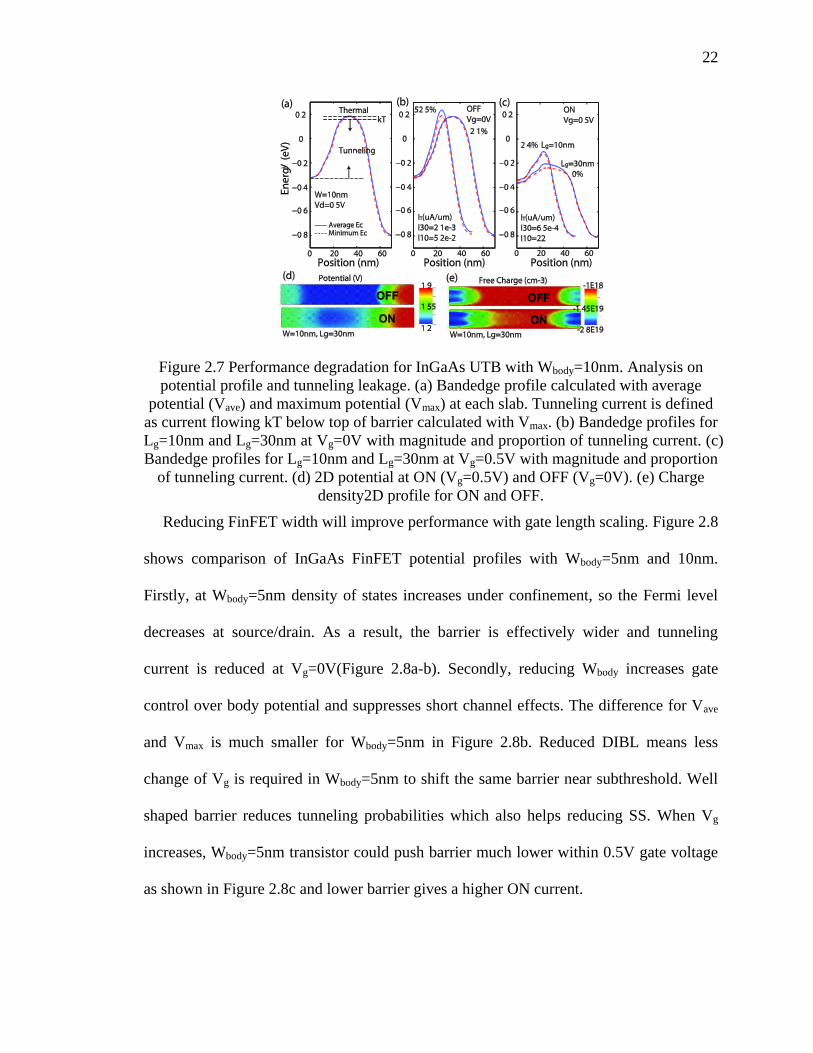
2.7 Performance degradation for InGaAs UTB with Wbody=10nm. Analysis on
potential profile and tunneling leakage. (a) Bandedge profile calculated with
average potential (Vave) and maximum potential (Vmax) at each slab. Tunneling
current is defined as current flowing kT below top of barrier calculated with
Vmax. (b) Bandedge profiles for Lg=10nm and Lg=30nm at Vg=0V with
magnitude and proportion of tunneling current. (c) Bandedge profiles for
Lg=10nm and Lg=30nm at Vg=0.5V with magnitude and proportion of tunneling
current. (d) 2D potential at ON (Vg=0.5V) and OFF (Vg=0V). (e) Charge
density2D profile for ON and OFF. ..........................................................................22
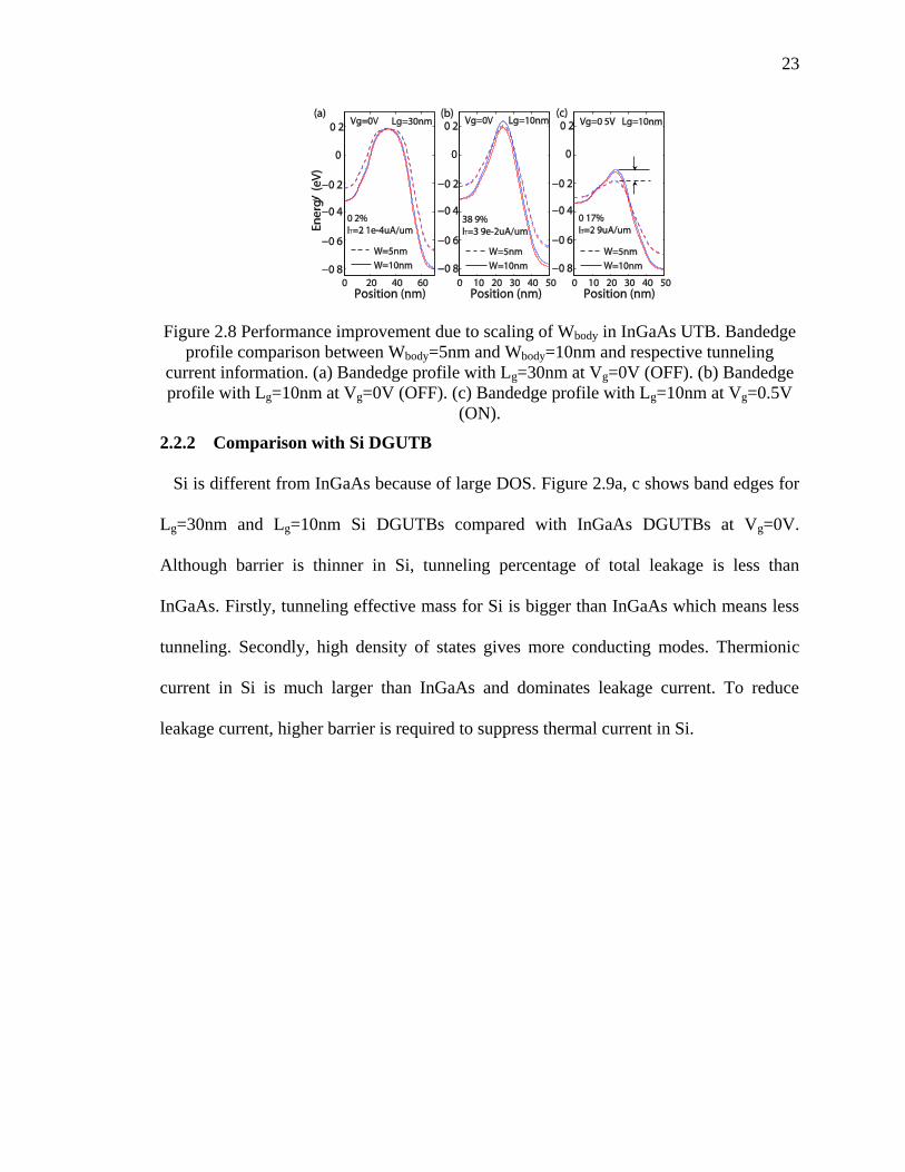
2.8 Performance improvement due to scaling of Wbody in InGaAs UTB. Bandedge
profile comparison between Wbody=5nm and Wbody=10nm and respective
tunneling current information. (a) Bandedge profile with Lg=30nm at Vg=0V
(OFF). (b) Bandedge profile with Lg=10nm at Vg=0V (OFF). (c) Bandedge
profile with Lg=10nm at Vg=0.5V (ON). ..................................................................23

xii
xii
Figure ............................................................................................................................. Page
2.9 Comparison of Si and InGaAs UTB gate length scaling at Wbody=5nm. (a-d) Band
edge profiles for (001)/<100> Si UTB with Lg=10nm and 30nm at Vg=0V and
0.5V, compared with InGaAs at the same Lg and Vg. Deviation for two potential
profiles is bigger for Si due to higher channel charge density (Blue: Ec-Vave, red:
Ec-Vmax). (e) Effects of DIBL for Si (dashed line) and InGaAs (solid line) UTBs.
(f) Si and InGaAs UTBs I-V at different Vd. Shifting of Vth indicates stronger
DIBL for Si. ..............................................................................................................24
2.10 Source starvation in InGaAs DGUTB. (a) Comparison of IV characteristics at
Vd=0.7V. (b-c) Band profiles for InGaAs and Si DGUTB at Vg=0.1, 0.3, 0.5,
0.7V. Because of higher drain bias, high doping regions of InGaAs with ND1 are
increased to 30nm. Device length for InGaAs DGUTB is 90nm. ............................26
2.11 Comparison of InGaAs 2D UTB and 3D FinFET with different heights at
Lg=15nm. (a) InGaAs FinFET with W=5nm and W=10nm at different heights.
Current of FinFET normalized by height to compare with UTB at the same
width. (b) Charge profiles for FinFET with different height and width at TOB at
Vg=0.5V. ..................................................................................................................27
2.12 Geometries of InGaAs nanowire for VCA and random alloy. (a) Cross section of
3×3 InGaAs nanowire for VCA. (b) VCA for contacts and random alloy for
channel. (c) Displacement of atoms in channel which is relaxed by VFF. ...............27
2.13 Transmission of InGaAs nanowires shown in Figure 2.12. (a) Transmission of
pure VCA. Transmission is integer number which corresponds to the number of
modes at the energy. (b) With random alloy, the transmission is reduced due to
alloy scattering and reflection at the VCA-RA boundaries. (c) Transmission
after relaxation in the RA region. .............................................................................28
2.14 Geometry of InGaAs MOSFET simulated with VCA and with RA at channel.
When RA is included in device, the thickness in periodic direction is defined
with 1 and 2 unit cells. ..............................................................................................29
2.15 Results calculated with semiclassical potential. (a) IV characteristics for InGaAs
MOSFET with VCA and RA of different seeds. (b) Charge density for OFF
state. Only half of the device is shown. (c) Charge density for ON state. Only
half of the device is shown. .......................................................................................30
2.16 Transmission and current spectrum at OFF state. (a) Electron density for one of
the 1uc device. Band profile is calculated with VCA band edges. (b)
Transmission is reduced at higher energies due to alloy scattering. Transmission
is increased at lower energies due to tunneling. (c) Current spectrum shows
tunneling peaks due to random alloy. .......................................................................30

xiii
xiii
Figure ............................................................................................................................. Page
2.17 (a) IV characteristics in linear scale. (b) The semiclassical band profile at ON
state. (c) Current spectrum from the VCA and two examples for the 1UC and
2UC cases which show lower current than the VCA. ...............................................31
2.18 Calculate equilibrium lattice constant for InGaAs. Results are converged with
respect to supercell sizes. ..........................................................................................32
2.19 Equilibrium lattice constant calculated for (a) In53Ga47As and (b) In65Ga35As.
The values predicted by VFF match well with experimental values. .......................32
2.20 Local conduction band minimum for InGaAs nanowire of different diameters. .......33
2.21 Local band minimum and number of In atoms in each slab. .....................................33
2.22 Simulation flow and the local electron density for 3nm × 3nm nanowire. ................34
2.23 Transmission function for structure in Figure 2.22. The transmission through
random alloy nanowire shows resonance tunneling features. ...................................34
3.1 . Comparison of published TFET channel current per unit width versus gate-to-
source voltage for (a) p-channel [40, 41] and (b) n-channel [39, 42-46]
transistors. Dashed lines bordering the shaded area indicate measured high-
performance (HP) and low-power (LP) 32-nm node MOSFET technology[47].
The black dashed lines are measured characteristics for I-MOS transistors. [7] ......37
3.2 Comparison of simulated TFET channel current per unit width versus gate-to-
source voltage for (a)p-channel and (b)n-channel transistors. [7] ............................38
3.3 Illustration of electron-hole duality and convergence issure for full quantum self-
consistent simulation.(a) Geometry of 10nm width UTB and local density of
states under homogeneous potential. (b) Charge density normalized for each
slab showing inhomogeneous charge distribution near the interface due to
density penetration into bandgap. .............................................................................39
3.4 (a) Device geometry of L shaped TFET. (b) Band profile plotted along dashed
line in (a). 4nm InAs and 10nm AlGaSb keeps staggered band alignment at
interface. ....................................................................................................................41
3.5 Comparison of quantum transport between DNL model and NEGF shows effects
of tunneling model. (a) IV characteristic for different undercut lengths. (b) Band
to band electron generation rate for Luc=10nm at Vg=0.15V and Vg=3V. (c)
Potential for tunneling junction at Vg=0.15V and Vg=3V. Contour lines are
spaced at equal spacing. ............................................................................................44

xiv
xiv
Figure ............................................................................................................................. Page
3.6 Effects of underlap (Ld) length. (a) IV characteristics with different drain length.
(b) Current spectrum for Ld=20nm at Vg=0. (c) Current spectrum for Ld=0 at
Vg=0. .........................................................................................................................45
3.7 Ambipolar current mechanisms and optimizations on doping, material, geometry.
(a) Effects of source materials and source doping profile. (b) Effects of drain
width and drain voltage. (c) Effects of supply voltage and high doping extension.
Current is higher at Ld=0 than Ld=20nm at OFF state after including Lex. (d)
Current spectrum after including high doping extension at drain contacts. .............47
3.8 (a) Structure for gate-recessed vTFETs. Arrows show current flow with (dash
black) and without (dash red) vertical drain contact. (b-c) UTB and NW TFETs.
...................................................................................................................................48
3.9 Simulated gate-recessed vTFETs compared with experimental measurements and
effects of serial resistance. ........................................................................................49
3.10 (a) Effects of drain doping and drain extension length at Vd=0.5V. Leakage
currents result from parasitic (b) ambipolar tunneling and (c) direct source-drain
tunneling. ..................................................................................................................49
3.11 (a) IV characteristics for n-type and p-type L-shaped TFETs shown in Fig. 1a. (b)
Extracted SS. .............................................................................................................50
3.12 (a) IV characteristics of n-type and p-type TFETs with double gate UTB
structures. (b) Extracted SS. ......................................................................................50
3.13 (a) IV-characteristics for single gate UTB TFETs. (b) Performance
improvements of UTB TFETs due to δ doping, shifted gate position and
increased gate length. ................................................................................................51
3.14 Band diagrams illustrating effects of δ doping and gate length in the UTB TFETs
shown in Fig. 6. .........................................................................................................51
3.15 (a) IV characteristics for NW TFETs. (b) Modification of band edges with body
thickness in UTB and diameters in NW. ..................................................................51
4.1 Stacked DFT DOS and DFT/TB bandstructure comparison. (a) DOS within
muffin-tin radius of Sm/Se and interstitial DOS. (b) DOS within Se atom
decomposed by angular momentum. (c) DOS within Sm atom decomposed by
angular momentum. (d) Band structure by spdfs*_SO TB model without strain
(black) and DFT band structure without strain (red). E=0 at top of valence band. ..57

xv
xv
Figure ............................................................................................................................. Page
4.2 Comparison of bandgap modulations with strain calculated by DFT and TB. (a)
Bandgap extracted from DFT and TB bandstructure under hydrostatic and
uniaxial strain. (b) TB bandstructure with ε=-3% compressive hydrostatic strain
(ax=ay=az=(1+ε)×a0). (c) TB bandstructure with ε=-3% compressive uniaxial
strain in growth direction (ax= (1+ε)×a0; ay=az=a0). Dashed lines show bulk
band edges in (b, c). ..................................................................................................58
4.3 Transport simulation for SmSe with hydrostatic strain. (a) Simulated structure in
and 6nm channel super cell in transport simulation. (b) Real and imaginary band
structure for 0% and -3% hydrostatic strain. (c) Transmission with 0V and
0.05V linear drop potential. (d) Vd=0.05V, spectral current, dJ/dE, with linear
drop potential. ...........................................................................................................59
5.1 Principle of CBRAM. Directions of metal ion diffusion and electron conduction.
[73] ............................................................................................................................61
5.2 Typical IV characteristics of CBRAM showing bipolar asymmetric
programming/erase feature. [75] Reprinted from Microelectronic Enginnering,
88 (5), pp814-816, Y. Bernard,V.T. Renard,P. Gonon,V. Jousseaume “Back-
end-of-line compatible Conductive Bridging RAM based on Cu and SiO2”(2011)
with permission from Elsevier. .................................................................................63
5.3 Simulation flow. Structures and charge profiles are generated by MD simulations.
The electrostatic potential is calculated based on atomic charges. Current is
calculated by NEGF and conductance is extracted. ..................................................65
5.4 Bond length and bond angle in amorphous SiO2 generated by ReaxFF. (a)
Geometry of amorphous SiO2. (b-c) Distribution of bond length. (d-e)
Distribution of bond angle. .......................................................................................67
5.5 Bandstructure for β-cristobalite obtained with parameters of O’Reilly and
Robertson[93]. This parameter set captures band position and could serve as
initial values for our TB parameterization. ...............................................................68
5.6 Bandstructure for 4 different crystalline SiO2 calculated by LDA. .............................69
5.7 Copyright © 2015, IEEE. Comparison of bandstructure calculated by optimized
TB parameters and DFT. Two crystalline SiO2 are calculated by the same set of
parameters. ................................................................................................................69
5.8 Bond radius in TB determines number of neighbor atoms coupled. ...........................70
5.9 Effects of confinement simulated with environmental dependent TB with 2nd
nearest neighbor model. [27] ....................................................................................71

xvi
xvi
Figure ............................................................................................................................. Page
5.10 Comparisons of Cu nanowire bandstructures calculated with DFT and TB. ............72
5.11 (a) Relaxation of grain boundary. Atom positions of top and bottom layers are
fixed. Periodic boundary condition is applied to directions parallel to GB. N
layer atoms from the GB are allowed to move. (b-d) Total potential energies for
(b) Ʃ3 (48 atoms), (c) Ʃ5 (40 atoms) and (d) Ʃ17a (136 atoms) GBs when N
layers of atoms are relaxed. ......................................................................................75
5.12 Extract Fermi level from density calculation. (a) Density of states spectrum. (b)
Cumulative total electron states. ...............................................................................76
5.13 Geometry generation. (a) Generate random seed → Voronoi diagram → Divide
original geometry into grains. (b) Simulation domain with leads attached. .............77
5.14 Definition of special grain boundaries. (a) Bamboo and random GBs. (b) Tilt and
twist GBs. ..................................................................................................................78
5.15 Resistance of (a) tilt and (b) twist GBs. .....................................................................78
5.16 (a) Resistance of GBs with general rotations. (b) Voronoi diagram for random
GBs with 4 grains. (c) Voronoi diagram for bamboo GBs with 4 grains. ................79
5.17 Bandstructure of Cu2O simulated with GGA and Hybrid functional (VASP
results calculated by Yaohua Tan). Only Hybrid functional result shows
bandgap close to experimental value. [136] .............................................................81
5.18 Crystal structure constructed from ATK builder. (a) Primitive unit cell of Cu2O.
(b) Primitive unit cell of CuO. (c) Antiferromagnetic unit cell for CuO. Thick
arrows indicate orientations of local magnetic moments. Thin arrows along [011]
direction shows atom chain with strongest superexchange. .....................................82
5.19 Bandstructure of Cu2O calculated with (a) ATK with LDA+U (b) ELK with
LDA+U compare to ref [136] with HSE. Results of (b) is calculated with crystal
structure from Wyckoff [143] with 11×11×11 k point and plane wave cut-off
roughly 400eV. .........................................................................................................83
5.20 Comparison of bandstructure calculated by HSE (HSE06 in VASP) and LDA+U
(ELK). Bandstructure of LDA+U has been modified with scissor operation to
match band gap with HSE. ........................................................................................83
5.21 Density of state for Cu2O and contributions of O and Cu atom to each band. ..........84
5.22 Geometry of Cu2O unit cell. Based on the decomposition of bandstructure, sp3d
5
TB model is used and coupled atoms up to 3rd
nearest neighbor are included.
Bandstructure after optimization captures important band features of DFT. ...........85

xvii
xvii
Figure ............................................................................................................................. Page
5.23 Copyright © 2015, IEEE. Diffusion of Cu atoms in SiO2 at t=0, 250, 500,
1000ps. Si and O atoms are not plotted for better visibility. (a) Distance between
electrodes is 1.5nm in initial structure. (b) Clusters are formed in SiO2. Two
electrodes are not connected by filaments. (c) Two electrodes are connected by
Cu filaments. The connectivity is plotted based on a coupling radius of 0.39nm.
(d) More filaments are formed. .................................................................................86
5.24 Copyright © 2015, IEEE. (a) Current for structures at Fig.3 at Vd=-1V. (b) Total
transmission at t=0ps and t=250ps. ...........................................................................86
6.1 SiGe with RH1 ordering generated by NEMO5. .........................................................87
6.2 Grains of SiGe with different ordering directions in RH2 ordering. (a) Each color
shows a grain with uniform ordering direction. (b) SiGe with RH2 ordering. .........88
6.3 SixGe1-x with x=0.2, 0.5, 0.8. Each chunk with 2 grains with degree of
ordering=0.9. Ordering direction are (1,1,1) (-1,-1,1) (-1,1,-1) (1,-1,-1) with
probabilities (0.2609, 0.3043, 0.2174, 0.2174) .........................................................89
xviii
xviii
ABSTRACT
Jiang, Zhengping. Ph.D., Purdue University, December 2015. Multi-Scale Simulations
For High Efficiency Low Power Nanoelectronic Devices. Major Professor: Gerhard
Klimeck.
Silicon based CMOS technology has been the driven force for semiconductor industry
for decades. With higher degree of integration, transistors working under low supply
voltage are desired to reduce power consumption. FinFET has been introduced to
suppress the short channel effects and quantum tunneling; devices like Tunneling FET
(TFET) and Piezoelectronic Transistor have been designed to achieve the subthreshold
swing (SS) below 60mV/dec; novel memory cells like conductive bridging RAM
(CBRAM) are able to operate at lower voltages and are more scalable than flash memory.
In this work, several emerging logic and memory devices have been studied. The
devices are optimized for high efficiency low power applications. Non-equilibrium
Green’s function formulism with empirical tight binding (ETB) basis is used for quantum
transport. The scaling of InGaAs FinFET is studied within virtual crystal approximation
in the ballistic limit. The effects of random alloy scattering are discussed. The
heterojunction TFETs are designed to achieve both low SS and high on-current. SmSe is
parameterized to reproduce the metal insulator transition in Piezoelectronic Transistor.
Copper is parameterized with the environmental dependent tight binding model and used
for the study of grain boundary resistance in interconnects. Finally to study the resistive

xix
xix
switching of CBRAM, functionalities to import structures generated by Molecular
Dynamics simulations and perform quantum transport have been developed. Calculations
are done with efficient offloading scheme to accommodate the memory and speed
requirements for realistic geometries.

1
1
1. INTRODUCTION
1.1 Scaling of MOSFET and requirements for low power devices
Si based MOSFET has been the most important device in the semiconductor industry
history. Scaling of MOSFET has enabled the integration of high density of transistors in a
single chip. As a result, modern circuits could accomplish more and more functionalities,
while the cost is reduced. In 2011, Intel unveiled the world’s first 3-D transistor in a high
volume logic process with 22nm Tri-Gate transistor. Innovation in semiconductor
technology has revolutionized our lives.
However, higher order of integration brings about another problem. Modern circuit
faces severe problem of power consumption. As computer speed increases, power
consumption also increases aggressively (Figure 1.1). To reduce power consumption,
transistors are required to operate in lower supply voltage. However, logic device must
maintain certain ON/OFF current ratio (~104) to distinguish logic states. For MOSFET,
the minimum subthreshold swing is 60mV/dec, which makes reducing supply voltage
below 0.5V extremely hard. As transistor scales down, subthreshold swing is getting
worse because of short channel effects and leakage due to tunneling. As a result, the
supply voltage has stopped to scale at around 1V for long time.

1
1
Figure 1.1 Power consumption of top 10 supercomputer (Nov. 2013). Source:
http://www.top500.org/
To continue Moore’s law, innovations are required to control short channel effects and
reduce tunneling to keep subthreshold swing close to or below 60mV/dec. New materials
have been explored to increase ON current e.g. InGaAs[1], SiGe because of the high
mobility over Si as shown in Table 1.1. Different orientations have been explored to
reduce tunneling[2]. Optimizations of geometries are also actively studied. In Chapter 2
the short channel effects and tunneling of InGaAs NFET will be discussed in details. The
performance of InGaAs NFET will be optimized and compared with Si NFET.
Table 1.1 Mobility of different materials[3, 4]
Si Ge GaAs InP In0.53GaAs
e mob.
(cm2/Vs) 1600 3900 9200 5400 12000
m*e (mt/m0) 0.19 0.082 0.067 0.082 0.041
h mob. 430 1900 400 200 -

2
2
Figure 1.2 Electron and hole mobility versus lattice constant. The impact of biaxial strain
is indicated by an arrow representing increasing compressive biaxial strain.[1] Reprinted
by permission from Macmillan Publishers Ltd: Nature (479, 317–323
doi:10.1038/nature10677), copyright (17 November 2011)
1.1.1 Short channel effects
As the transistor is scaled down, one of the major short channel effects is drain
introduced barrier lowering (DIBL). DIBL has two effects on device performance. It will
firstly shift the threshold voltage. When channel length is further reduced, it will also
affect the subthreshold slope. Figure 1.3a shows IV curve for InGaAs and Si MOSFET
simulated in 2D double gate ultra-thin-body (UTB) geometry. Shift of threshold voltage
shows the effects of DIBL. Barrier height is changed with Vd even with the same gate
voltage. It is shown DIBL affects differently for different materials, which gives freedom
for optimization.

3
3
Copyright © 2015, IEEE
Figure 1.3 Effects of DIBL. (a) IV for InGaAs and Si UTB MOSFET with different Vd.
Shift of threshold voltage shows effects of DIBL. (b) Lowering of barrier due to Vd.
1.1.2 Complex bandstructure and tunneling current
Quantum tunneling is one of the fundamental effects in quantum mechanisms. As
shown in Ref. [5], as electron tunnels through a barrier, the electron wave will decay
according to its complex wave vectors. In Wentzel-Kramers-Brillouin (WKB)
approximation, for Zener tunneling [6], the transmission is , where
κ(x) is the imaginary wave vector. It has been shown that single band model with
parabolic band will underestimate tunneling probability[5]. Compared with the full band
tight binding model, for indirect bandgap materials like Si and Ge, it is even hard for fit a
single κ(x) as in Figure 1.4.

4
4
Figure 1.4 Complex bandstructure of In0.53GaAs and Si in 5nm UTB. (a) A single
imaginary band will connect conduction and valence band. (b) Imaginary bands cross
over each other. A single band could not be separated from other bands.
1.2 Emerging logic devices
Improving MOSFET will make subthreshold swing close to 60mV/dec, but that will
be the fundamental limitation for MOSFET. To reduce supply voltage further, new
device designs are required which is not limited by Boltzmann distribution of carriers in
contacts.
1.2.1 Tunneling FET
Tunneling FET (TFET) is one of the most promising devices which could provide SS
extremely low[7]. As shown in Figure 1.5 InAs UTB MOSFET and TFET with 10nm
width are simulated at the same gate bias. In MOSFET, the leakage current is flowing at
higher energies over the barrier, while in TFET bandgap of the source material will block
the high energy carriers which are distributed according to Boltzmann distribution. In this
condition, TFET gives 3 orders of magnitude smaller leakage current. Ideally, TFETs
should have a sharp turn on when conduction band edge of channel is lower than valence
band edge in source. However, there are new leakage mechanisms: firstly carrier still
could tunneling through gate barrier like in MOSFET; secondly, when bandgap is small

5
5
and drain bias is big, addition tunneling happens near channel drain junction like shown
in Figure 1.5 which is the main leakage path here.
In Chapter 3, a novel design of TFET with gate electric field in-line with tunneling
direction is discussed. The advantages and limitations of the L-shaped TFET have been
studied. A multi-physics simulation flow is designed to model the broken gap TFET.
Figure 1.5 Comparison of MOSFET and TFET density of states (logarithm scale) and
current spectrum (logarithm scale) at Vd=0.2V.
1.2.2 Piezoelectronic transistor
Another way to overcome the subthreshold limit is by internally boost the gate voltage
to generate larger barrier change than gate voltage change. One example is the
Piezoelectronic Transistor (PET) [8-10].
In the PET the limitation on the Subthreshold Swing (SS) imposed by the thermal tail
of Boltzmann distribution is overcome through internal transduction. A small gate
voltage (Vg) is transduced to an acoustic wave through a high-performance piezoelectric
(PE) actuator fabricated from a relaxor piezoelectric material. The expansion of the PE
layer exerts pressure to a channel layer consisting of a piezoresistive (PR) material
capable of undergoing a pressure-induced insulator to metal transition. Rare earth
chalcogenide PR materials - such as SmSe and SmTe - can vary conductance by several

6
6
orders of magnitude when subjected to modest pressure changes[11]. Such conductance
change is predicted to exceed the maximum conductance gain achievable in the MOSFET,
which is 10 × Vg/60mV.
Chapter 4 focuses on the material properties of SmSe, which is the key element of
PET. The electronic bandstructure of SmSe has been modeled with ab initio approach.
The metal-insulator transition of SmSe has been explained in terms of strain response of
electronic bandstructure. SmSe has been parameterized in empirical tight binding basis
which is well suited for large scale transport simulations.
1.3 Emerging memory devices
Memory is an indispensable part of computer system, especially non volatile memory
(NVM), which retains stored information even when power is cut-off. Floating gate flash
memory is the dominating NVM in market, widely used in all sizes of electronic devices.
However, scaling of flash memory is far behind scaling of logic devices. Also flash
memory requires very high operation voltage. New memory cells which are more
scalable, low power are in demand. Many new memory technologies have been proposed.
Table 1.2 lists some of the most promising designs. PCM and RRAM attract a lot of
interests.
Table 1.2 ITRS 2013 emerging memory technologies. Green color shows the advantages
and red color shows major drawbacks.
Prototypical Emerging
FeRAM STT-
MRAM
PCRAM Ferroelectric
memory
Redox
memory
Macromolec-
ular memory
Scalability ?
MLC
Integration
Cost
Endurance
7
7
In Chapter 5 the Conductive Bridging RAM (CBRAM) is introduced. Modeling of
CBRAM requires multi-physics, multi-dimensional efforts. In this work, CBRAM based
on SiO2/Cu is simulated. A complete simulation flow has been proposed to model both
the electrochemical process and the electronic properties. Parameter sets for Cu and SiO2
have been developed and enhanced. The Cu parameterization has been tested in modeling
grain boundaries of nanoscale interconnect. The results are compared with literature
results and show good agreement with ab inito simulations.
1.4 Electronic Bandstructures
When device is at nanometer scale, the atoms in active region are countable. Atomistic
simulation is nature choice for future computer aided design. Depending on size of
system, different methods are available with different accuracies and convey different
physics.
1.4.1 Density Functional Theory
For system with small amount of atoms usually below a few hundreds, density
functional theory (DFT) could be used. In DFT, properties of a many electron system are
determined by functionals or density here. The Kohn-Sham DFT reduces the many-body
problem of interacting electrons into non-interacting electrons moving in an effective
potential called Kohn-Sham potential[12, 13]. The non-interacting particles will generate
the same density as the original system. The effective potential includes the external
potential and effects of the Coulomb interactions. However, the exact functionals for
exchange and correlation are not known except for the free electron gas. Approximations
are used including local-density approximation (LDA), generalized gradient
approximations (GGA), metaGGA and hybrid functionals.

8
8
Varieties of quantum chemistry and solid state physics software are available.
Different basis sets have been used. Earlier calculations use atomic orbitals composed of
Slater-type orbitals (STOs); later STOs are approximated by linear combinations of
Gaussian-type orbitals (GTOs); in addition to localized basis sets, plane-wave basis (PW)
sets can also be used. Typically, a finite number of plane-wave functions are used defined
by a specific cutoff energy; in the linearised augmented planewave (LAPW) method[14],
based on atomic spheres approximation (ASA) the basis is atomic-like within muffin-tin
spheres and connected to planewaves outside.
Table 1.3 Quantum chemistry softwares used in this work with major features (Hartree-
Fock (HF); molecular mechanics (Mol. mech.))
basis HF post-HF Mol. mech.
ELK FP-LAPW Yes No No
VASP PW Yes Yes Yes
ATK NAO/EHT No No Yes
SIESTA NAO No No Yes
1.4.2 Empirical Pseudo-potential Method
The Empirical Pseudopotential Method (EPM) was originally developed as an
efficient way to solve the Schrodinger’s equation for bulk crystals. It assumes that the
core electrons are tightly bound to the nuclei (frozen core approximation) and the valence
electrons are only influenced by an effective potential. This potential could be
represented by a truncated Fourier series. The expansion coefficients are generally fitted
to reproduce important material properties.
9
9
1.4.3 Extended Hückel Theory
Extended Hückel method (EHT) is another semi-empirical method to calculate
electronic properties of materials. In the EHT model the Hamiltonian is expanded in a
basis of local atomic orbitals. The orbitals are not required to be orthogonal to each other.
EHT requires very small number of parameters, which makes the fitting process much
easier. However, because EHT uses non-orthogonal basis, transport simulation requires
calculation of overlap matrix. This potentially increases the memory and turnaround time.
1.4.4 Empirical tight binding
DFT has successfully predicted properties of material properties, but the total atoms in
calculation are limited to a few hundreds. For more realistic device, empirical tight
binding method could be highly parallelized and handle hundred thousand atoms in
quantum transport and over million atoms in electronic calculation [15-17]. The empirical
tight binding method or the modified linear combination of atomic orbitals (LCAO)
method published by Slater and Koster (SK)[18] is an extension of Bloch’s original
LCAO method[19]. The parameters could be obtained by fitting to electronic energy
bands and density of states [20-23]. In the Naval Research Laboratory tight-binding
(NRL-TB)[24, 25], total energy is included as fitting target and distance and
environment-dependent SK parameters are used to include transferability. Also there are
some recent works which generate SK parameters from directly mapping of DFT[26] and
include environmental dependency for metals[27].
10
10
1.5 High performance computation
1.5.1 NEMO5 and nanoHUB.org
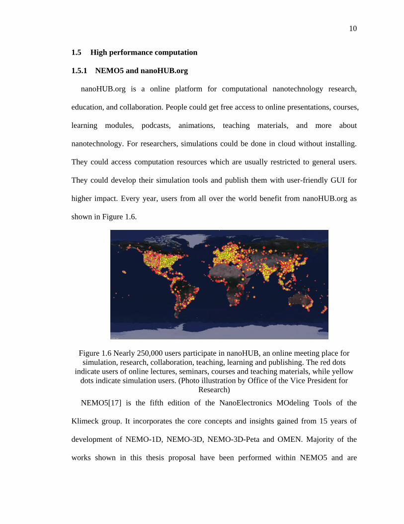
nanoHUB.org is a online platform for computational nanotechnology research,
education, and collaboration. People could get free access to online presentations, courses,
learning modules, podcasts, animations, teaching materials, and more about
nanotechnology. For researchers, simulations could be done in cloud without installing.
They could access computation resources which are usually restricted to general users.
They could develop their simulation tools and publish them with user-friendly GUI for
higher impact. Every year, users from all over the world benefit from nanoHUB.org as
shown in Figure 1.6.
Figure 1.6 Nearly 250,000 users participate in nanoHUB, an online meeting place for
simulation, research, collaboration, teaching, learning and publishing. The red dots
indicate users of online lectures, seminars, courses and teaching materials, while yellow
dots indicate simulation users. (Photo illustration by Office of the Vice President for
Research)
NEMO5[17] is the fifth edition of the NanoElectronics MOdeling Tools of the
Klimeck group. It incorporates the core concepts and insights gained from 15 years of
development of NEMO-1D, NEMO-3D, NEMO-3D-Peta and OMEN. Majority of the
works shown in this thesis proposal have been performed within NEMO5 and are
11
11
incorporated into the NEMO5 development. Some of the functionalities of NEMO5 are
accessible through online simulation tools in nanoHUB.org.
1.5.2 Parallel computing
In the area of computational nanoelectronics, accurate band models are desired to
describe the simulated system. Meanwhile complicated models require more
computational resources. Nowadays, it is extremely difficult to achieve meaningful
modeling without massive parallelization. Different parallelization schemes have been
used for the studies in this thesis including Message Passing Interface (MPI) and Open
MPI. Computation is further accelerated by offloading the computationally heavy matrix
multiplication operations into coprocessors. The speed up with offloading is presented in
Chapter 5.
1.6 Contributions of the present work and thesis organization
As the scaling of Si MOSFET becomes more and more difficult, semiconductor
industry has been looking for new approaches to continue the Moore’s law. This
requirement imposes great challenges as well as great opportunities to the advance of
computational nanoelectronics. On one hand, there is the growing need for more accurate
modeling. As device sizes shrink, the granularity of materials starts to show profound
effects; random dopants, roughness, grain boundaries, impurities all bring uncertainties to
the device performances. Atomistic modeling is getting more and more recognition. As
new materials are utilized and devices with new physics are developed, predictive
simulations are desired for prototyping and path finding study. Even for the traditional
materials and technologies, existing modeling frameworks need recalibration with more
advanced models. On the other hand, modeling approaches have limitations by

12
12
themselves. New modeling approaches need to be developed to fulfill the growing need
to match new experimental observations. While the complexities of models are limited by
the computational resources; due to the balance of accuracy and productivity, no single
modeling approach is able to fulfill all the simulation requirements.
This thesis work deals with the dilemma from the following aspects:
(1) Path-finding studies on the new materials and new devices with the atomistic
modeling approaches.
(2) Design modeling flows with high accuracy while maintain manageable
computational complexities.
(3) Explore the multi-physics multi-dimensional modeling flow to break the
limitation of individual approach.
The thesis is organized as follows:
In Chapter 2, the design space of InGaAs MOSFET is explored to suppress short
channel effects and tunneling. Empirical tight binding model and effective mass model
are compared for this application and the limitations of both models are revealed. Effects
of alloy scattering are studied with the atomistic approach.
In Chapter 3, the semiclassical potential is used for fast prototyping of the novel L-
shaped Tunneling FET. The advantages and limitations of the TFET for continuous
scaling are studied. The non-equilibrium Green’s function approach is compared with the
non-local dynamic band to band tunneling model. This study proves the necessity of full
quantum transport approach in predictive modeling of TFETs.
In Chapter 4, the working principles of the Piezoelectronic Transistor are introduced
which could achieve subthreshold swing below 60mV/dec. One of the key component

13
13
materials SmSe has been modeled using the ab inito approach with LDA+U functional. A
physics based process has been used to parameterize SmSe in the empirical tight binding
basis.
In Chapter 5, the multi-physics flow is designed to modeling the Conductive Bridging
RAM. Cu and SiO2 are parameterized in the empirical tight binding basis. Grain
boundary resistance is also studied with the obtained Cu parameter set. The results are
compared with more advanced DFT-NEGF approach. Both models show consistent
results while our approach allows for large scale simulations.
In Chapter 6, future works are presented.
1.7 Reuse of published work
The work in this thesis is based on the papers published in different journals. Figures
and contents have been reused from these publications in this work. The permissions for
the reuse of contents and figures from the publishers have been obtained which are
present in the Appendix B.
14
14
2. SCALING OF INGAAS FINFET
2.1 Methods for alloy simulation
Figures and portions of this chapter have been reproduced verbatim from Electron
Devices, IEEE Transactions on (Volume:62 , Issue: 2 ) “Tunneling and Short Channel
Effects in Ultrascaled InGaAs Double Gate MOSFETs” Zhengping Jiang, Behtash
Behin-Aein, Zoran Krivokapic, Michael Povolotskyi, Gerhard Klimeck. Copyright 2015
IEEE.
Scaling of Si based MOSFET has been driven force for semiconductor industry.
FinFET with 22nm channel length has been announced and further scaling of channel
length is down to 7nm. To continue scaling, InGaAs attracts great attention as alternative
channel material and efforts have been made for fabricating non-planar devices [28-30].
With shrinking size, devices will operate beyond drift diffusion regime and quantum
effects start to show profound impacts; material properties will alter dramatically under
confinement. Understanding of FinFET scaling behavior by quantum transport simulation
is in demand.
Unlike binary materials, InGaAs is alloy as shown in Figure 2.1a. It could be
considered as GaAs binary material with Ga atoms randomly replaced by In according to
certain composition.

15
15
(a) (b)
Figure 2.1 Illustration of InGaAs in random alloy and VCA. (a) Random alloy crystal
with In atoms replaced by Ga. (b) VCA crystal with two types of atom: As and virtual
atom InGa.
Simulation of alloy material usually has two types of methods. Firstly, randomness of
alloy is ignored. Effective mass approximation (EM) and virtual crystal approximation
(VCA) [31] fall into this category. Otherwise, alloy is simulated by replacing atoms
explicitly[32, 33] which is called random alloy method (RA) in this work.
EM used to provide good approximation when device dimension is big and transport
happens near bottom of conduction band. However, under confinement strong non-
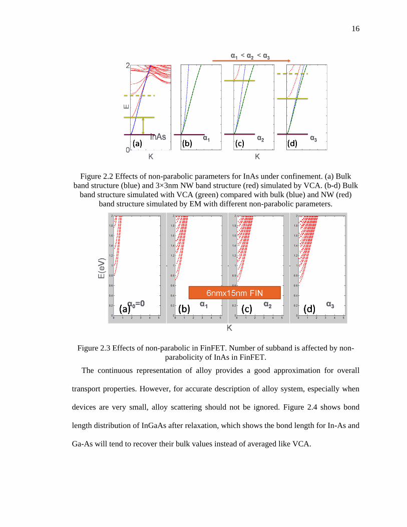
parabolicity must be taken into consideration. Figure 2.2a shows band structure of bulk
InAs and in 3×3nm nanowire. Confinement raises the subbands and changes the effective
masses. Solid and dashed horizontal lines show the first and second subband positions. In
EM if non-parabolic parameter is not accurate, the subband position will be
overestimated greatly as shown in Figure 2.2b-d with increasing α, similarly for subbands
in FinFET as shown in Figure 2.3.
VCA is a better approximation. Figure 2.1b shows the VCA crystal with only two
types of atoms. The TB parameter is usually obtained by simple interpolation rule for
InxGa1-xAs: VInGaAs=x·VInAs+(1-x)·VGaAs. Higher order correction and bowing factor
could be included[31]. This method strongly depends on transferability of TB
parameterization.
16
16
Figure 2.2 Effects of non-parabolic parameters for InAs under confinement. (a) Bulk
band structure (blue) and 3×3nm NW band structure (red) simulated by VCA. (b-d) Bulk
band structure simulated with VCA (green) compared with bulk (blue) and NW (red)
band structure simulated by EM with different non-parabolic parameters.
Figure 2.3 Effects of non-parabolic in FinFET. Number of subband is affected by non-
parabolicity of InAs in FinFET.
The continuous representation of alloy provides a good approximation for overall
transport properties. However, for accurate description of alloy system, especially when
devices are very small, alloy scattering should not be ignored. Figure 2.4 shows bond
length distribution of InGaAs after relaxation, which shows the bond length for In-As and
Ga-As will tend to recover their bulk values instead of averaged like VCA.
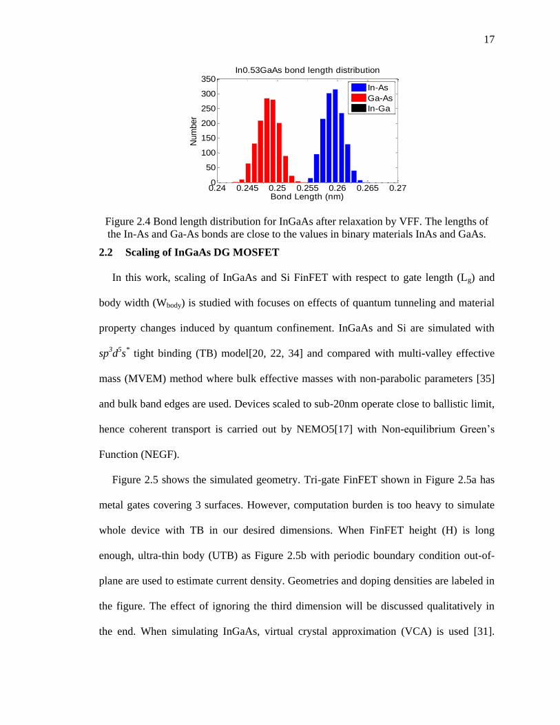
17
17
Figure 2.4 Bond length distribution for InGaAs after relaxation by VFF. The lengths of
the In-As and Ga-As bonds are close to the values in binary materials InAs and GaAs.
2.2 Scaling of InGaAs DG MOSFET
In this work, scaling of InGaAs and Si FinFET with respect to gate length (Lg) and
body width (Wbody) is studied with focuses on effects of quantum tunneling and material
property changes induced by quantum confinement. InGaAs and Si are simulated with
sp3d
5s
* tight binding (TB) model[20, 22, 34] and compared with multi-valley effective
mass (MVEM) method where bulk effective masses with non-parabolic parameters [35]
and bulk band edges are used. Devices scaled to sub-20nm operate close to ballistic limit,
hence coherent transport is carried out by NEMO5[17] with Non-equilibrium Green’s
Function (NEGF).
Figure 2.5 shows the simulated geometry. Tri-gate FinFET shown in Figure 2.5a has
metal gates covering 3 surfaces. However, computation burden is too heavy to simulate
whole device with TB in our desired dimensions. When FinFET height (H) is long
enough, ultra-thin body (UTB) as Figure 2.5b with periodic boundary condition out-of-
plane are used to estimate current density. Geometries and doping densities are labeled in
the figure. The effect of ignoring the third dimension will be discussed qualitatively in
the end. When simulating InGaAs, virtual crystal approximation (VCA) is used [31].
0.24 0.245 0.25 0.255 0.26 0.265 0.270
50
100
150
200
250
300
350
Bond Length (nm)N
um
ber
In0.53GaAs bond length distribution
In-As
Ga-As
In-Ga

18
18
Figure 2.5c shows the In53Ga47As bulk band structure calculated from VCA. The band
edges extracted from TB are compared with values used in MVEM, where the non-
parabolic parameter is roughly approximated as 1/Eg. TB describes more accurately band
non-parabolicity away from band minima, but available parameterization does not
reproduce Г-L valley splitting accurately. Transport in Si is considered in two directions
as shown in Figure 2.5a. For [100], both TB and MVEM are considered. Three valleys
are included independently with effective masses (valley 1: mx/my,z=0.916/0.19, valley 2:
my/mz,x=0.916/0.19, valley 3: mz/mx,y=0.916/0.19), each with 2 fold degeneracy. For
[110], transport direction is not the same as the semi-principal axes of the ellipsoid and
hence there are no appropriate masses. Only TB is used in this orientation.
Figure 2.5 Simulated device geometries and In53Ga47As parameters. (a) Left: 3D FinFET
dimensions with simulated crystal directions for InGaAs and Si. Right: Cross section of
FinFET showing gate position. (b) DGUTB dimensions and doping densities for InGaAs
and Si. (c) In53Ga47As bulk bandstructure calculated by VCA with sp3d
5s
* basis and
extracted band parameters defined in the figure. Also parameters used for different
valleys in effective mass approximation for InGaAs. Difference in bandgap between two
models is due to ignoring spin orbit coupling in TB-VCA.
Figure 2.6 summarizes the transfer characteristics. For all devices gate length (Lg) is
scaled from 30nm to 7nm. All curves are shifted to match the same leakage level (Ioff) of

19
19
100nA/um, so Vg is actually Vg’=Vg-Vth in all figures; Vth is threshold voltage. Figure
2.6a-b show InGaAs FinFET with Wbody=10nm and 5nm simulated by MVEM and TB.
Figure 2.6c-d show [100]/(100) and [110]/(100) Si FinFET with Wbody=5nm simulated by
TB. The [100]/(100) FinFET TB result is compared with MVEM. From Figure 2.6, all
devices at short gate length show higher subthreshold swing (SS) and lower ON current
(Ion). Comparison between Wbody=10nm and 5nm InGaAs FinFET (Figure 2.6a-b) shows
thinner Wbody suffers less degradation upon scaling. Figure 2.6b-c show Si has higher Ion
at long gate length than InGaAs, but InGaAs will outperform at short gate length.
Switching to [110] direction does not show improvements for Si FinFET. Comparisons
between two band models show MVEM model matches quite well for InGaAs at
Wbody=10nm and give qualitatively the right trend at Wbody=5nm. For [100] Si MVEM
matches well with TB even at Wbody=5nm.

20
20
Figure 2.6 Effects of gate length scaling from Lg=30nm to Lg=7nm for different body
widths, directions and materials. Calculations are done with TB and compared with
MVEM in (a-c). (a) InGaAs UTB with Wbody=10nm. (b) InGaAs UTB with Wbody=5nm.
(c) Si (001)/<100> UTB with Wbody=5nm. (100) (d) Comparison between InGaAs (line
with markers) and Si(1-10)/<110> (solid and dashed lines) DGUTBs at different doping
conditions. Wbody=5nm, Lg=10nm calculated with TB for all devices.
2.2.1 Scaling of gate length
Degradation of SS and Ion at short Lg is due to combined effects of drain introduced
barrier lowing (DIBL) and increasing of tunneling leakage. Current of FinFET is
composed of thermal current and tunneling current (IT). To evaluate tunneling, top of
barrier (TOB) should be defined. However band edges across the body are not
homogeneous as shown in Figure 2.7d, which plots the electrostatic potential (V(x))
profile at Vg=0V and 0.5V for InGaAs FinFET with Wbody=10nm, Lg=30nm. Conduction
band (Ec) calculated from averaged potential (Vave(x)) and maximum potential(Vmax(x))
for each slab along transport direction are plotted in Figure 2.7a. To avoid overestimating

21
21
effects of tunneling, in this work the energy threshold for IT is chosen as kT below the
top of barrier calculated from Vmax(x).
Under effects of DIBL, depletion region of channel-drain junction extends into
channel. Gate voltage has to reduce more to increase channel barrier height, because gate
voltage will deplete drain contact at the same time and drain capacitance is big due to
high charge density. Figure 2.7b shows the band edges at Vg=0V for Lg=30nm and 10nm.
Though channel is depleted, strong deviation of Vave and Vmax magnitude at Lg=10nm
indicates only surface potential is following change of Vg, while body potential is
affected by Vd and remain unchanged. SS will increase accordingly when gate control is
weak as DIBL is getting stronger.
Tunneling leakage further enhance effects of DIBL. According to TOB model, if
current is purely thermionic, barrier height should be the same at the same current level.
However thinner barrier allows more carriers to tunnel through, so barrier height has to
increase to maintain the same leakage level. This means gate voltage has to be further
decreased when effects of DIBL are already strong. With high barrier, both tunneling and
thermal components will decrease at the same time. Figure 2.7b shows at Lg=10nm
barrier height is higher than at Lg=30nm and thermal current is only half of the value at
Lg=30nm, rest of leakage current is due to tunneling.
When transistor turns on at Vg=Vd=0.5V (Figure 2.7c), for Lg=10nm FinFET because
barrier is already higher at OFF state and gate voltage has to balance effects of DIBL
when increasing, for the same Vg swing total barrier change is smaller at Lg=10nm as
shown in Figure 2.7c. At Vg=0.5V total current is dominated by thermal current and
higher barrier means lower thermal current or lower Ion at shorter gate length.
22
22
Figure 2.7 Performance degradation for InGaAs UTB with Wbody=10nm. Analysis on
potential profile and tunneling leakage. (a) Bandedge profile calculated with average
potential (Vave) and maximum potential (Vmax) at each slab. Tunneling current is defined
as current flowing kT below top of barrier calculated with Vmax. (b) Bandedge profiles for
Lg=10nm and Lg=30nm at Vg=0V with magnitude and proportion of tunneling current. (c)
Bandedge profiles for Lg=10nm and Lg=30nm at Vg=0.5V with magnitude and proportion
of tunneling current. (d) 2D potential at ON (Vg=0.5V) and OFF (Vg=0V). (e) Charge
density2D profile for ON and OFF.
Reducing FinFET width will improve performance with gate length scaling. Figure 2.8
shows comparison of InGaAs FinFET potential profiles with Wbody=5nm and 10nm.
Firstly, at Wbody=5nm density of states increases under confinement, so the Fermi level
decreases at source/drain. As a result, the barrier is effectively wider and tunneling
current is reduced at Vg=0V(Figure 2.8a-b). Secondly, reducing Wbody increases gate
control over body potential and suppresses short channel effects. The difference for Vave
and Vmax is much smaller for Wbody=5nm in Figure 2.8b. Reduced DIBL means less
change of Vg is required in Wbody=5nm to shift the same barrier near subthreshold. Well
shaped barrier reduces tunneling probabilities which also helps reducing SS. When Vg
increases, Wbody=5nm transistor could push barrier much lower within 0.5V gate voltage
as shown in Figure 2.8c and lower barrier gives a higher ON current.
23
23
Figure 2.8 Performance improvement due to scaling of Wbody in InGaAs UTB. Bandedge
profile comparison between Wbody=5nm and Wbody=10nm and respective tunneling
current information. (a) Bandedge profile with Lg=30nm at Vg=0V (OFF). (b) Bandedge
profile with Lg=10nm at Vg=0V (OFF). (c) Bandedge profile with Lg=10nm at Vg=0.5V
(ON).
2.2.2 Comparison with Si DGUTB
Si is different from InGaAs because of large DOS. Figure 2.9a, c shows band edges for
Lg=30nm and Lg=10nm Si DGUTBs compared with InGaAs DGUTBs at Vg=0V.
Although barrier is thinner in Si, tunneling percentage of total leakage is less than
InGaAs. Firstly, tunneling effective mass for Si is bigger than InGaAs which means less
tunneling. Secondly, high density of states gives more conducting modes. Thermionic
current in Si is much larger than InGaAs and dominates leakage current. To reduce
leakage current, higher barrier is required to suppress thermal current in Si.

24
24
Figure 2.9 Comparison of Si and InGaAs UTB gate length scaling at Wbody=5nm. (a-d)
Band edge profiles for (001)/<100> Si UTB with Lg=10nm and 30nm at Vg=0V and 0.5V,
compared with InGaAs at the same Lg and Vg. Deviation for two potential profiles is
bigger for Si due to higher channel charge density (Blue: Ec-Vave, red: Ec-Vmax). (e)
Effects of DIBL for Si (dashed line) and InGaAs (solid line) UTBs. (f) Si and InGaAs
UTBs I-V at different Vd. Shifting of Vth indicates stronger DIBL for Si.
Figure 2.9b, d compare band edges at Vg=0.5V. At Lg=30nm although barrier for Si
FinFET is higher than InGaAs, current is still larger in Si due to more conducting modes.
However as Lg is reduced to 10nm, Si current goes lower than InGaAs. At Lg=10nm,
Figure 2.9e shows output characteristics of Si and InGaAs DGUTBs and Figure 2.9f
shows Si and InGaAs DGUTBs with Vd=0.3-0.5V. It is shown DIBL is more severe in Si

25
25
than InGaAs. As gate length scales down, Si barrier increasing at Vg=0.5V due to DIBL
is more obvious and Ion will become smaller than InGaAs.
2.2.3 Source Starvation
DOS bottleneck is known for III-V transistors[36], which could lead to source
starvation at high bias. InGaAs and Si DGUTBs are simulated with Vd=0.7V in Figure
2.10a. The potential changes are shown in Figure 2.10b-c at different gate biases.
Because of low density in InGaAs, the inversion layer capacitance is small. As gate
voltage increases, more barrier reduction is desired to sustain enough charges to carry
current. At Vg=0.7V, band minimum in InGaAs channel has been the same as in the
contact. Increasing gate voltage will not further increase charge density[37]. While for Si
DGUTB current could still increase because channel could hold more charges. Source
starvation does not happen at Vd=0.5V. Firstly transverse confinement increases channel
density of states which delays onset of source starvation. Secondly as gate voltage
increases, density in source contact will reduce because of reduced confinement in
transport direction. Fermi level in source will increase to maintain charge neutrality. As a
result, source starvation will happen in higher biases because of reduction in source
barrier. Increasing source doping will have similar effects and prevent current saturation
at high bias, but it will also degrade performances as shown in Figure 2.6d.
26
26
Figure 2.10 Source starvation in InGaAs DGUTB. (a) Comparison of IV characteristics at
Vd=0.7V. (b-c) Band profiles for InGaAs and Si DGUTB at Vg=0.1, 0.3, 0.5, 0.7V.
Because of higher drain bias, high doping regions of InGaAs with ND1 are increased to
30nm. Device length for InGaAs DGUTB is 90nm.
2.2.4 Comparison of 3D and 2D geometries
UTB is used as approximation for FinFET because of computation burden of TB.
Since MVEM are proved to be qualitatively accurate, we could simulate FinFET with full
structure and compare it with UTB results after normalization by height. Figure 2.11
shows simulated InGaAs FinFET with Wbody=5nm, H=5, 10, 15, 20, 30nm and
Wbody=10nm, H=10nm. It is shown with H>2W I-V curves will converge to UTB results.
For H<2W, FinFET performance will be better than UTB. This is because firstly extra
gate provide better electrostatic control when height is small. Also different confinement
change DOS near corners. As height increases, corner effects will be small compared
with current carried by body charges after normalization.
2.3 Atomic simulations of alloy scattering
2.3.1 Effects of alloy scattering to transport
Alloy scattering has big effects on transport properties of transistors. Firstly a
homogeneous InGaAs nanowire is simulated without external potential. Figure 2.12a
shows the nanowire simulated with VCA. In Figure 2.12b, length of 7nm channel in the

27
27
middle is replaced by random alloy InGaAs. The RA part is relaxed by valence force
field method with two boundaries at interface with VCA regions fixed. Figure 2.12c
shows displacement after relaxation.
Figure 2.11 Comparison of InGaAs 2D UTB and 3D FinFET with different heights at
Lg=15nm. (a) InGaAs FinFET with W=5nm and W=10nm at different heights. Current
of FinFET normalized by height to compare with UTB at the same width. (b) Charge
profiles for FinFET with different height and width at TOB at Vg=0.5V.
Figure 2.12 Geometries of InGaAs nanowire for VCA and random alloy. (a) Cross
section of 3×3 InGaAs nanowire for VCA. (b) VCA for contacts and random alloy for
channel. (c) Displacement of atoms in channel which is relaxed by VFF.
Transmissions are calculated for VCA and RA before and after relaxation as shown in
Figure 2.13. Without RA region, the transmission is integer for all energy range. When
RA region is included, the transmission for higher energy is reduced significantly, but for

28
28
lower energy transmission only reduces slightly, possibly because similar orbital
contribute to the lower energy band in both VCA and RA while orbitals for higher
energies are mixed up.
Figure 2.13 Transmission of InGaAs nanowires shown in Figure 2.12. (a) Transmission
of pure VCA. Transmission is integer number which corresponds to the number of modes
at the energy. (b) With random alloy, the transmission is reduced due to alloy scattering
and reflection at the VCA-RA boundaries. (c) Transmission after relaxation in the RA
region.
Then effect of alloy scattering is tested in MOSFET. Similar to previous simulations,
Figure 2.14 shows the simulated 2D double gate MOSFET with VCA and VCA+RA.
This time the length of RA is increased into source and drain underlap regions, but the
structure is not relaxed. For 2D simulation, the thickness of RA MOSFET is taken to be 1
and 2 unit cell. Ideally this dimension should be as thick as possible because periodicity
does not exist in this direction in real RA. A choice of 2D geometry is only limited by
computational resources. Convergence with respect to thickness should be further tested.

29
29
Figure 2.14 Geometry of InGaAs MOSFET simulated with VCA and with RA at channel.
When RA is included in device, the thickness in periodic direction is defined with 1 and 2
unit cells.
Current is calculated by NEGF on top of the same semiclassical potential for all
geometries. Figure 2.15a shows the IV characteristics. RA devices with different
thicknesses are simulated with 3 random seeds. It is shown with the same potential the
threshold voltage is shifted for RA devices. On current is also reduced for RA devices.
With 2 unit cell layers, the threshold shift is smaller. Charge density in Figure 2.15b-c
shows strong fluctuation and localization due to alloy. Charge density is much smoother
in the 2 unit cell device.
Figure 2.16 shows the reason for higher current at OFF state for RA devices.
Transmission shows that, for high energies alloy scattering will reflect injection electrons,
so transmission is reduced. For energies close to and below bandedge of VCA InGaAs,
transmission for VCA will decay, but with the same potential RA devices give higher
current at this energy range. This is because RA does not have accurate band edges;
instead band edge at the top of barrier is determined by local composition. The In rich

30
30
region will possess lower band edge than VCA and allows more current to flow through
channel barrier.
Figure 2.15 Results calculated with semiclassical potential. (a) IV characteristics for
InGaAs MOSFET with VCA and RA of different seeds. (b) Charge density for OFF state.
Only half of the device is shown. (c) Charge density for ON state. Only half of the device
is shown.
Figure 2.16 Transmission and current spectrum at OFF state. (a) Electron density for one
of the 1uc device. Band profile is calculated with VCA band edges. (b) Transmission is
reduced at higher energies due to alloy scattering. Transmission is increased at lower
energies due to tunneling. (c) Current spectrum shows tunneling peaks due to random
alloy.

31
31
For ON current, Figure 2.17c shows RA samples will have lower current over top of
barrier, which is consistent with previous observation.
Figure 2.17 (a) IV characteristics in linear scale. (b) The semiclassical band profile at ON
state. (c) Current spectrum from the VCA and two examples for the 1UC and 2UC cases
which show lower current than the VCA.
2.3.2 Random alloy in InGaAs nanowire
2.3.2.1 VFF Relaxation
To generate 3D InGaAs nanowire with random alloy, the equilibrium lattice constant
is firstly calculated with VFF model. The Keating energy per unit cell is calculated with
different lattice constant. The equilibrium lattice constant is fitted to get the lowest
energy. As shown in Figure 2.18, the result is tested for different sizes of supercell and
the calculate is well converged.

32
32
Figure 2.18 Calculate equilibrium lattice constant for InGaAs. Results are converged with
respect to supercell sizes.
The calculated equilibrium bond length for In53Ga47As is a=0.58569nm and for
In65Ga35As is a=0.59047nm.
(a) (b)
Figure 2.19 Equilibrium lattice constant calculated for (a) In53Ga47As and (b) In65Ga35As.
The values predicted by VFF match well with experimental values.
2.3.2.2 Local bandstructure
With the calculated lattice constant for In53Ga47As, square nanowires with diameters
of 2nm, 3nm and 4nm are constructed and relaxed with VFF. After relaxation, it is
possible to repartition the nanowires into slabs by every 4 layers of atoms. For each slab,
the bandstructure is calculated and the local conduction band minimum is extracted. This
local band minimum is plotted in Figure 2.20.
0.584 0.586 0.588 0.59
0.128
0.13
0.132
0.134
0.136
0.138
0.14
0.142
0.144
0.146
Lattice Constant (nm)
Ke
atin
g E
ne
rgy p
er
Un
it C
ell
(eV
)
30X30X30 unit cells
20X20X20 unit cells
0.57 0.58 0.59 0.6 0.610.1
0.15
0.2
0.25
0.3
0.35
0.4
0.45
0.5
0.55
0.6
Lattice Constant (nm)
Keating E
nerg
y p
er
Unit C
ell
(eV
)
0.58 0.59 0.6 0.610.1
0.15
0.2
0.25
0.3
0.35
0.4
0.45
0.5
0.55
0.6
Lattice Constant (nm)
Keating E
nerg
y p
er
Unit C
ell
(eV
)

33
33
From Figure 2.20, it is clear that the local properties of nanowires are very different
because the In and Ga atoms are not homogeneously distributed at each slab. This effect
is stronger in nanowires with smaller cross sections. Figure 2.21 plots also the number of
In atoms in each slab. The local band profile shows correlation with In composition as the
binary material InAs has much lower band edge than GaAs.
Figure 2.20 Local conduction band minimum for InGaAs nanowire of different diameters.
Figure 2.21 Local band minimum and number of In atoms in each slab.
In Figure 2.22, a simulation flow is proposed for random alloy InGaAs nanowire
transistors. The center of the device is relaxed random alloy structure. The leads are
0 5 10 15 20 25 301
1.2
1.4
1.6
1.8
Position (nm)
Local conduction b
and (
eV
)
2X2 nm2
3X3 nm2
4X4 nm2
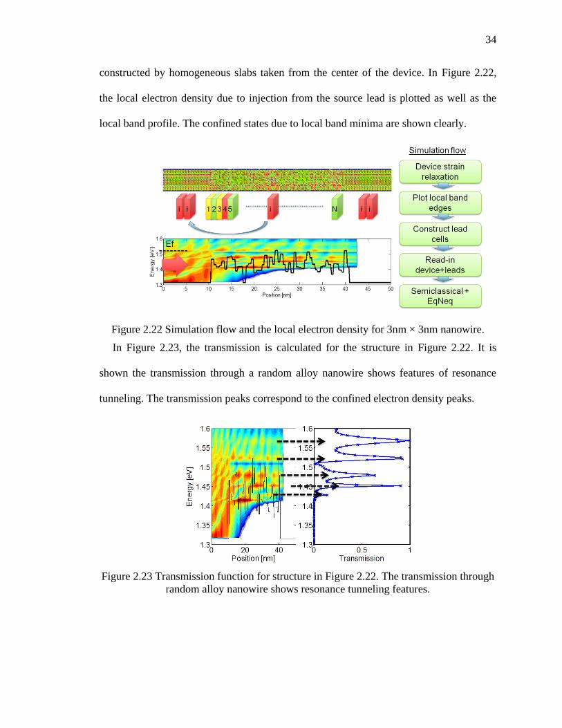
34
34
constructed by homogeneous slabs taken from the center of the device. In Figure 2.22,
the local electron density due to injection from the source lead is plotted as well as the
local band profile. The confined states due to local band minima are shown clearly.
Figure 2.22 Simulation flow and the local electron density for 3nm × 3nm nanowire.
In Figure 2.23, the transmission is calculated for the structure in Figure 2.22. It is
shown the transmission through a random alloy nanowire shows features of resonance
tunneling. The transmission peaks correspond to the confined electron density peaks.
Figure 2.23 Transmission function for structure in Figure 2.22. The transmission through
random alloy nanowire shows resonance tunneling features.

35
35
2.4 Summary and outlook
In summary with fixed leakage level FinFET ON current degrades with shrinking gate
length. Gate control over channel is weakened by DIBL. Channel barrier is getting more
and more transparent to quantum tunneling. Tunneling leakage further enhances the
effects of DIBL. Reducing FinFET width proves to suppress short channel effects, limit
tunneling and improve performance. InGaAs could outperform Si when channel length is
short. To certain scale MVEM is still valid and predict qualitatively the right trend for
both InGaAs and Si. With H>2Wbody in FinFET corner effects are small and conclusions
based on UTB match with 3D geometry.
As the dimensions of InGaAs FinFET or nanowire are reduced to a few nanometers,
the local variations due to alloy scattering cannot be ignored. Simulations with random
alloy structure relaxed by VFF are important to capture the localization effects. For
random alloy simulation, the lead structures must be chosen carefully with either the
general lead method[38] or homogeneous lead as proposed in this work. For the
homogeneous lead, multiple lead slabs must be considered and the averaged result is
taken to capture the variations.
36
36
3. OPTIMIZATION OF LSHAPED TFET
3.1 Overview
Figures and portions of this chapter have been reproduced verbatim from Electron
Devices, IEEE Transactions on (Volume: 62, Issue: 8) “Quantum Transport in
AlGaSb/InAs TFETs With Gate Field In-Line With Tunneling Direction” Zhengping
Jiang, Yeqing Lu, Yaohua Tan, Yu He, Michael Povolotskyi, Tillmann Kubis, Alan C
Seabaugh, Patrick Fay, Gerhard Klimeck. Copyright 2015 IEEE.
Figures and portions of this chapter have been reproduced verbatim from Device
Research Conference (DRC), 2013 71st Annual 145-146 “Atomistic simulation on gate-
recessed InAs/GaSb TFETs and performance benchmark” Zhengping Jiang, Yu He,
Guangle Zhou, Tillmann Kubis, Huili Grace Xing, Gerhard Klimeck. Copyright 2015
IEEE.
In the review paper by A. Seabaugh and Q. Zhang[7] two figures show the state-of-
the-art TFETs performance comparison against CMOS. From these data, it is shown that
most of the demonstrated TFETs with SS<60mV/dec are of the ON current level in
pA/µm, far away from neither high-performance nor low-power applications. Higher ON
current could be achieved in low bandgap materials like InGaAs [39], but it does not
show a sub-60mV/dec SS due to a parasitic tunneling mechanism involving traps in the
source junction.

37
37
Copyright @ 2010, IEEE
Figure 3.1 . Comparison of published TFET channel current per unit width versus gate-
to-source voltage for (a) p-channel [40, 41] and (b) n-channel [39, 42-46] transistors.
Dashed lines bordering the shaded area indicate measured high-performance (HP) and
low-power (LP) 32-nm node MOSFET technology[47]. The black dashed lines are
measured characteristics for I-MOS transistors. [7]
Simulations show promising performances for low bandgap materials or
heterostructures. Depending on geometry, materials, doping profile there are huge design
space to optimize TFET performances.
Among all the material systems, heterostructure of AlGaSb/InAs and GaSb/InAs
attracts great attention. Researchers from University of Notre Dame designed a novel top-
gated TFET based on p-type AlGaSb and n-type InAs [48, 49] which gives record high
ON current.

38
38
Copyright @ 2010, IEEE
Figure 3.2 Comparison of simulated TFET channel current per unit width versus gate-to-
source voltage for (a)p-channel and (b)n-channel transistors. [7]
3.1.1 Electron-hole duality
Unlike in MOSFET where electrons and holes are well separated by bandgap and
transport usually involves one type of carriers, tunneling carriers reside inside the
bandgap in TFETs and are therefore difficult to classify as either electrons or holes.
Figure 3.3a shows TB local density of states along the center of a 10nm thick lateral PN
heterojunction with GaSb and InAs without any potential. As commonly adopted, the
intrinsic level is calculated as Ei = (Ec+Ev) / 2 + 0.5 * Vt * log(Nv/Nc) and it is taken as
the separation for electron (e-) and hole (h
+). Assume Fermi level is at E=0eV, integration
of free charge density at each atom layer through device is plotted in Figure 3.3b. By
looking at the positive charge, hole density first drops then increases. It drops due to
reflection of electron wave near barrier. Deficiency of charge will generate a built-in field

39
39
and if this charge is used in solving Poisson equation, potential will drop to increase
charge density. Also from Figure 3.3a it is shown InAs density will penetrate into GaSb
bandgap. Because the density is far from Ef, when it is populated as electrons, the
negative charge is small, but when it is populated as holes it will generate the hole
density peak in Figure 3.3b. Similarly for the electron density spike on the InAs side due
to penetration of GaSb density. This dipole near interface will further push down the
potential in the arrow direction shown in Figure 3.3a. However in ballistic simulation,
carriers could not change energy when propagating, so carriers will not fill the potential
well which results in insufficient feedback when solving Poisson. Potential will be further
pushed down. These two effects combined will results in unphysical divergence of
electrostatic potential.
Figure 3.3 Illustration of electron-hole duality and convergence issure for full quantum
self-consistent simulation.(a) Geometry of 10nm width UTB and local density of states
under homogeneous potential. (b) Charge density normalized for each slab showing
inhomogeneous charge distribution near the interface due to density penetration into
bandgap.
3.2 Simulation methods
To relieve the problem, carriers could be thermalized to fill the potential well by
including phonon scattering, but it will also impose huge computational burden. Instead
in this work quasi Fermi level is introduced implying quasi-thermal equilibrium. Since

40
40
tunneling charge is quite small and channel is mostly in equilibrium with drain contact in
nTFET, channel could be considered as non-degenerate and Boltzmann distribution could
be applied. As a result, charge density is approximated as
.
Quantum effects are included as corrections in two ways. Band edges takes confinement
effects into account. The effective density (Nc) is treated as fitting parameter to preserve
degeneracy energy ηc=Ec-Ef (ηv=Ev-Ef) at each contact as predicted by tight binding for
respective doping densities. This is crucial step to ensure an accurate result, since the
current in TFET largely depends on the energy range which allows tunneling and the
range is controlled by bandedges at two contacts. The charge density is then coupled to
Poisson equation to achieve a self-consistent potential profile. NEGF calculations then
run on top of the potential. This method is sufficiently accurate for a quick solution and
comparable to Drift-Diffusion formulism in computational resources. With effects of
confinement partially covered through electrostatics by introducing corrected parameters,
tunneling current is calculated by NEGF.
3.3 Simulation of L-shaped TFETs
Simulations based on drift-diffusion and the dynamic nonlocal path band-to-band
model (DNL) [50] have been performed and minimum SS of 7mV/dec is predicted [51].
Without considering effects of quantization, the results revealed dependencies of the
device on electrostatics and geometry variations. Further modeling requires inclusion of
quantum effects and generalized tunneling formalisms. Tunneling is sensitive to material
properties like bandgap and effective mass which will change dramatically in nanoscale
devices subjected to quantum confinement especially for III-V materials with strong non-
parabolic dispersion[52]. The tunneling formulism adopted in DNL band-to-band model

41
41
assumes a classical particle-like trajectory which would underestimate possible tunneling
paths under some conditions.
Figure 3.4a shows the simulated structure. The tunneling structure consists of AlGaSb
source with Ts=20nm, WGaSb=10nm and InAs drain with TInAs=4nm. A p-type δ-doping
layer is inserted in the source to improve electric field at junction which is composed of
Tδ=1nm with peak doping Nδ=5×10¹⁹
cm-3
and 1nm decay with Nδ=1.9×10¹⁹
cm-3
at each
side. The channel under gate (Lg) and spacer oxide (Lox) and drain extension or underlap
(Ld) are doped with ND1=5×10¹⁷
cm-3
. An extra high doping extension (Lex) is included in
some simulation configurations with ND2=4×10¹⁸
cm-3
. Channel is gated with oxide of
EOT=1nm and spacer of Lox=10nm is used.
Figure 3.4 (a) Device geometry of L shaped TFET. (b) Band profile plotted along dashed
line in (a). 4nm InAs and 10nm AlGaSb keeps staggered band alignment at interface.
3.3.1 Band offset
In this device, band alignment at heterojunction is re-evaluated with sp3s
* model with
spin orbit coupling. Bulk band offset is adjusted to 150eV for GaSb/InAs in this
parameterization by shifting diagonal energy of InAs. The key benefit for using AlGaSb
(GaSb)/InAs is the staggered (broken) gap heterojunction in bulk measurement, as
tunneling probability will reduce exponentially with barrier thickness. As shown in
Figure 3.4b bandstructure calculation results in a staggered heterojunction with an offset
of ΔE=215meV between 10nm AlGaSb and 4nm InAs after confinement, which is much

42
42
larger than the effective offset when confinement is not considered. When InAs increases
to 6nm, the heterojunction offset reduced to ΔE=122meV. If 10nm GaSb and 4nm InAs
is used, the value will reduce to ΔE=53meV, but is still a type II alignment. The broken
gap (type III) alignment of ΔE=-40meV could be recovered when 10nm GaSb and 6 nm
InAs is used. These predictions are based on purely quantization. High doping could
introduce bandgap narrowing and strain could also change the bandgap.
3.3.2 Comparison with dynamic nonlocal path band-to-band model
Comparison is made for two models in the same structures. NEGF calculation is done
with NEMO5 and DNL calculation is done with Sentaurus TCAD. The structure is
similar as shown previously, with NA=4×1018cm
-3, Nδ=6×10¹⁹
cm-3
, ND=5×1017cm
-3 and
Ld=30nm. To highlight the effects of current and tunneling mechanisms, differences
between two potentials are minimized by applying the same effective mass and band
edges. The primary deviation in density is the extra generation charges in TCAD, but
these charges are small compared with thermal charges especially when TFET is in
subthreshold regime.
Figure 3.5a plots the comparison of Id-Vg for different Lu/Lg at Vd=0.3V. ON current
for two models are similar which indicates that in III-V, WKB used in DNL and NEGF
predict consistent tunneling current. Especially for heterojunction where the tunneling
distance is short and wave vectors are small, the effect of complex bandstructure is very
small. However the subthreshold performance is quite different. Best matching is
achieved only with Luc=20nm, Lg=30nm. This difference is because DNL model
underestimate direct source-drain tunneling which is major leakage at OFF state when
gate length is short.
43
43
Figure 3.5b, c show electron generation rate in DNL model at Vg=0.15 and 0.3V.
Vg=0V is not plotted which has almost no electron band to band generation observed
through device. At Vg=0.15V, the generation mainly happens near the tunneling junction
and also small generation observed in undercut region. At Vg=0.3V, most of the
generation happens near the tunneling junction. Based on the DNL tunneling model, the
tunneling direction is calculated opposite to the gradient of the valence band energy and
the path is approximated by a straight line with starting position at the vertex. Figure 3.5d
and e shows potential profile near the tunneling junctions at Vg=0.15 and 0.3V. Contour
lines with equal potential spacing are plotted. Electric field lines are normal to the
contour lines. Figure 3.5e shows strong electric field is generated at high Vg. From
Figure 3.5d, e, the contour lines are mostly flat in GaSb, so electrons tunneling vertically
through the junction with limited number of carriers tunneling towards drain sides.
Generation is mainly directly under gated drain region on top of source. While for NEGF,
tunneling is not limited by geometry, instead major leakage is tunneling from source to
drain reservoir through gate at this length scale as will be shown later, so large portion of
the tunneling current in NEGF model is prohibited in DNL due to the geometry.
Moreover, as shown in Figure 3.5d, e the red line indicates a minimum of potential,
which is at the position of δ doping. The appearance of δ doping layer creates a local
minimum of potential and hence the electric field gradient will point in the opposite
direction. This reduces tunneling since the electrons below the red line can only tunnel to
the source contact as defined by the electric field gradient. In DNL the source reservoir
of tunneling electrons is limited to area between δ doping peak and the hetero-junction.
Finally, as Luc is increased, the barrier at undercut region is getting longer and the direct

44
44
source drain tunneling is reduced to minimum. In this limit DNL and NEGF will reach
better agreement, e.g. Luc=20nm in Figure 3.5a.
Figure 3.5 Comparison of quantum transport between DNL model and NEGF shows
effects of tunneling model. (a) IV characteristic for different undercut lengths. (b) Band
to band electron generation rate for Luc=10nm at Vg=0.15V and Vg=3V. (c) Potential for
tunneling junction at Vg=0.15V and Vg=3V. Contour lines are spaced at equal spacing.
3.3.3 Effects of drain contact doping and geometry
Length of Ld plays an important role in decoupling gate and drain. Because charge
density is low in InAs, the screening length for electric field generated by gate drain
voltage difference (Vgd) is long. If Ld is not sufficient, change of Vg will shift the band
edge at drain contact. Figure 3.6a shows comparison of Id-Vg for different underlap
lengths ranging from 0nm to 50nm. At Vg=0V leakage current increases for Ld>0nm and
converges after Ld=20nm. At Vg>0.1V, all transistors show similar IV characteristics. At
Vg<0V, the ambipolar current will be higher for shorter Ld. Figure 3.6b-c show current

45
45
spectrum (dJ/dE) at Vg=0V for Ld=0nm and 20nm device. It is shown that for Ld=0nm
the main component of current is thermal current, while for Ld=20nm the main current is
tunneling current. At Ld=0nm, the potential profile at drain contact is coupled closely to
gate. The underlap region is fully depleted. In this condition tunneling is blocked by
bandgap of drain contact. As Ld increases continuously, bandedge at drain contact will
drop until Ld equals to screening length and charge neutral condition is fulfilled. Thermal
current will keep decreasing because of increasing potential barrier for hole transport and
tunneling current will increase because the energy window for tunneling is opened by
bandgap. The overall current will firstly drop then increase when tunneling current
surpasses thermal current. Ambipolar current here is not due to tunneling but thermal
current. This is shown from SS for electron and hole branches. Double arrows in Figure
3.6a show SS of 60mV/dec. For electron branch, SS value is smaller than 60mV/dec, but
for hole branch SS is over 60mV/dec.
Figure 3.6 Effects of underlap (Ld) length. (a) IV characteristics with different drain
length. (b) Current spectrum for Ld=20nm at Vg=0. (c) Current spectrum for Ld=0 at
Vg=0.
Inserting a high doping region before drain contact will also suppress gate drain
coupling. However, the effect of Ld will be different with the high doping extension (Lex).
Figure 3.7c shows IV for TFET with 4nm InAs drain, Ld=0nm, 20nm and Lex=20nm with

46
46
high doping ND2=4×10¹⁸
cm-3
. Different from Figure 3.6a, current for Ld=0nm at Vg=0V
is higher than Ld=20nm. Current spectrum in Figure 3.7d shows the reason. Extra high
doping region will reduce Debye length significantly, so even at Ld=0nm, the band edge
at drain is not increased. Instead, more tunneling current will occur because barrier length
is reduced with Ld. At the same time, thermal current is kept unchanged because of the
barrier at high doping region for hole transport, so ambipolar current does not appear
unless gate voltage is further reduced. As sketched in Figure 3.7c, there are three current
paths. The electron branch is labeled as one, which happens in source-channel junction.
When there is not high doping extension, the ambipolar branch comes from the third path.
When bandgap is wide or drain bias is small, e.g. WInAs=4nm with Vd=0.3V, the second
path which happens in channel drain junction is blocked. When Lex is included, the third
path will be suppressed as shown in Figure 3.7c. If bandgap is reduced (dashed line in
sketch) or drain bias is increased, the second path will be open.
3.3.4 Summary and Outlook
In this work, device performances of top-gated TFETs are evaluated by quantum
simulation. A simulation flow is designed combining efficient potential calculation and
NEGF. Comparison with the DNL model shows that in this structure, DNL model will
underestimate leakage current. Ambipolar current due to thermal emission and channel-
drain tunneling is discussed, which is controlled by doping condition and bandgap near
channel-drain junction. Device performances are optimized with respect to geometry and
materials.

47
47
Figure 3.7 Ambipolar current mechanisms and optimizations on doping, material,
geometry. (a) Effects of source materials and source doping profile. (b) Effects of drain
width and drain voltage. (c) Effects of supply voltage and high doping extension. Current
is higher at Ld=0 than Ld=20nm at OFF state after including Lex. (d) Current spectrum
after including high doping extension at drain contacts.
3.4 Comparison to other types of geometries
Recently a record high ON current of 180 µA/µm at Vds = 0.5 V has been reported in
InAs/GaSb n-type vertical TFETs with a recessed gate and the tunnel direction aligned
with the gate field [48] and for the first time GaSb/InAs p-type TFETs are also
experimentally demonstrated with sidewall gates and the tunnel direction perpendicular
to the gate field showing a highest ON current among III-V pTFETs. Experimental
InAsSb/GaSb nanowire TFETs [53] have also been studied as they are expected to
benefit from good electrostatic control. When TFETs are scaled to nanometer size, effects
of confinement and atomistic material properties cannot be ignored. In this paper, the

48
48
fabricated InAs/GaSb nTFETs with recessed gates are simulated and performances of
TFETs with different geometries are explored for both pTFET and nTFETs.
3.4.1 Simulations of gate-recessed vertical nTFETs
The simulated structure (Figure 3.8a) is L-shaped (L-TFET). Carriers flow from the
GaSb source (ts=10 nm, Ns1=1x10¹⁹
cm-3
, Ns2=4x10¹⁸
cm-3
) and tunnel vertically into the
InAs channel (tb=6 nm, Nc=1x10¹⁷
cm-3
). A gate is placed on top of the tunneling
junction. A 1-nm thick InP layer is included between the InAs channel and the gate stack
(4nm HfO2 and 1nm Al2O3) to reduce interface states (Dit). The n+InAs drain contact
region is doped with Nd=3x10¹⁹
cm-3
.
Figure 3.8 (a) Structure for gate-recessed vTFETs. Arrows show current flow with (dash
black) and without (dash red) vertical drain contact. (b-c) UTB and NW TFETs.
Simulation results show an Ion of 244 µA/µm and an Ioff of 1.7x10⁻³
µA/µm at Vg=Vd=
0.5 V with a minimum subthreshold swing (Smin) of 48.7 mV/dec (Figure 3.9a). The drain
contact resistance can reduce current at low Vd and high Vg, but it is observed to show
limited effects at Vd=0.5 V due to a tunnel current saturation (Figure 3.9b). Two leakage
mechanisms are identified to limit the OFF current: a) parasitic ambipolar tunneling
(Figure 3.10b) and b) direct source-drain tunneling (Figure 3.10c). The device
performance is expected to improve when the drain doping is reduced and the drain
extension is increased (Figure 3.10a). Removing the InP barrier from the drain contact
will also increase the ON current (Figure 3.9a).

49
49
Figure 3.9 Simulated gate-recessed vTFETs compared with experimental measurements
and effects of serial resistance.
Figure 3.10 (a) Effects of drain doping and drain extension length at Vd=0.5V. Leakage
currents result from parasitic (b) ambipolar tunneling and (c) direct source-drain
tunneling.
3.4.2 Performance benchmarking with UTB and NW TFETs:
The performance of n- and p-L-TFETs is benchmarked with ultra-thin body (UTB)
and nanowire (NW) TFETs. A constant EOT=0.6 nm is used for all devices. The vertical
drain contact is removed in the L-TFETs for the best device performance. The doping
densities in all devices are listed in Table 3.1. Figure 3.11 and Figure 3.12 show the
performances of the L-TFETs and double gate (DG) UTB TFETs with the extracted
subthreshold swing (SS). It is shown that L-TFETs possess SS < 60 mV/dec for large
bias ranges with body thickness up to tb= 6 nm. The pTFETs show better SS due to the

50
50
larger bandgap of GaSb. This bandgap blocks the leakage tunneling current and reduces
the ambipolar thermal current better. For DG-TFETs, the SS values are always larger
than 60 mV/dec. The body thickness should be limited below 10 nm for an effective gate
control.
Figure 3.11 (a) IV characteristics for n-type and p-type L-shaped TFETs shown in Fig. 1a.
(b) Extracted SS.
Figure 3.12 (a) IV characteristics of n-type and p-type TFETs with double gate UTB
structures. (b) Extracted SS.
Single gate UTB-TFETs show similar current levels, but with degraded SS (Figure
3.13a). The UTB-TFET performance is expected to improved by inserting δ-doping in
front of the tunneling junction, by shifting the gate position (Lshift in Figure 3.8b), or by
increasing the gate length. Figure 3.13b shows an improved SS when a 2 nm δ-doping
layer (1x10¹⁹
cm-3
), and a Lg of 15nm is used (see also the band diagrams and current
spectrum in Figure 3.14).
51
51
Figure 3.13 (a) IV-characteristics for single gate UTB TFETs. (b) Performance
improvements of UTB TFETs due to δ doping, shifted gate position and increased gate
length.
Figure 3.14 Band diagrams illustrating effects of δ doping and gate length in the UTB
TFETs shown in Fig. 6.
The NW-TFETs (dnw=3 nm) show better SS than UTB TFETs, but their current level
is several orders of magnitude smaller than the one of the other structures. Increasing the
diameter to 4 nm will increase Ion by a factor of 1000, since the band overlap at
GaSb/InAs interface is then reduced by 200 meV (Figure 3.15b).
Figure 3.15 (a) IV characteristics for NW TFETs. (b) Modification of band edges with
body thickness in UTB and diameters in NW.

52
52
3.4.3 Conclusions:
Fully atomistic simulations for realistically extended complex devices show the best
performing SSmin are summarized in Table 3.1. The L-shaped TFETs show best
performance; however, their scaling is limited by the undercut. The ON currents in UTB
TFETs are limited by source-gate coupling, which can be improved by including a δ-
doping layer. NW TFETs suffer from strong confinement effects, which reduce the ON
current densities significantly. Wire diameters of more than 10 nm are required to get the
broken-gap band alignment.
Table 3.1 Summary TFETs doping and performance (*Inw (µA/µm) normalized by
diameter)
tb nm SSmin Ns1 Ns2 Nc Nd Vd V Ion/Imax Ioff Lg nm Ion/Ioff
L-nTFET 4 41.5 1E19 4E18 1E17 5E18 0.3 137.8/693 1e-3 20 1.3e5
L-pTFET 2 29.6 1E19 5E17 5E17 1E19 0.3 105.7/174 1e-3 20 1.0e5
n-UTB 4 87.4 1E19 2E18 1E18 5E18 0.3 1.4/18.3 1e-3 10 1.4e3
P-UTB 4 69.4 5E18 1E18 2E18 1E19 0.3 4.1/21.4 1e-3 10 4.1e3
n-NW* 3 79.5 1E20 2E19 1E19 5E19 0.3 0.025/0.057 3.2e-5 10 7.8e2
p-NW* 4 61.1 5E19 1E19 2E19 1E20 0.3 1.28/4.89 1.9e-4 10 6.7e3
53
53
4. PIEZOELECTRONIC DEVICES
4.1 Introduction
Figures and portions of this chapter have been reproduced verbatim from Appl. Phys.
Lett. 102, 193501 (2013) “Electron transport in nano-scaled piezoelectronic devices”
Zhengping Jiang, Marcelo A. Kuroda, Yaohua Tan, Dennis M. Newns, Michael
Povolotskyi, Timothy B. Boykin, Tillmann Kubis, Gerhard Klimeck and Glenn J.
Martyna. Copyright 2013 American Institute of Physics.
For decades, scaling of the Si-based MOSFET has enabled an exponentially increasing
level of integration, packaging density and clock speed. Today heat dissipation prevents
any performance improvement through increasing clock frequency because the supply
voltage has reached the scaling limit of MOSFET technology and cannot be lowered
much below about 1 V without performance degradation. This fundamental power
consumption issue has spurred the exploration of alternative switching mechanisms.[54]
The recently proposed Piezoelectronic Transistor (PET)[9, 10] shows great potential to
achieve a high ON/OFF ratio with a small voltage swing. In the PET the limitation on
the Subthreshold Swing (SS) imposed by the thermal tail of Boltzmann distribution is
overcome through internal transduction. A small gate voltage (Vg) is transduced to an
acoustic wave through a high-performance piezoelectric (PE) actuator fabricated from a
relaxor piezoelectric material. The expansion of the PE layer exerts pressure to a channel

54
54
layer consisting of a piezoresistive (PR) material capable of undergoing a pressure-
induced insulator to metal transition. Rare earth chalcogenide PR materials - such as
SmSe and SmTe - can vary conductance by several orders of magnitude when subjected
to modest pressure changes.[55, 56] Such a conductance change is predicted to exceed
the maximum conductance gain achievable in the MOSFET, which is 10 × Vg/60mV.
The promising qualities of SmSe as a channel material have been experimentally
demonstrated in thin film[57] and bulk crystalline form.[11, 58] When a PET is scaled
down to nanometer size, quantum effects will dominate carrier dynamics and classical
transport models assuming a continuous medium will eventually fail to predict device
performance. Though the bulk properties of SmSe have been studied by density
functional theory (DFT)[59], quantum transport at realistic dimensions cannot be
performed at the DFT level due to its prohibitive computational burden and inability to
model non-equilibrium carrier transport. Approaches such as the empirical tight binding
(ETB) method may open the possibility for the modeling of realistically extended devices
provided that they can embody the physics underlying the piezoresistive effect. Indeed
ETB has been widely used in simulations of nanoelectronic devices[20, 60, 61].
4.2 Methods
In this work, the pressure induced Metal Insulator Transition in SmSe is modeled by
ETB. The effect arises from the high sensitivity of the deformation potential to strain
which rapidly shrinks the electronic bandgap. SmSe is parameterized for ETB[26] and
results are calibrated to DFT calculations which in turn agree well with experimental
measurements. Both ETB and DFT models capture the reported responses of the

55
55
bandgap to external pressures.[11] The non-equilibrium Green’s function (NEGF)
method is then used to study ballistic transport with NEMO5.[17]
Our ETB parameterization features a basis transformation from DFT, in a plane wave
representation, to an orthogonal TB basis – i.e. Löwdin orbitals[18] – and subsequent
refinement by numerical optimization. With band structures and wavefunctions obtained
from DFT calculations at the minimum-energy lattice constant, a DFT Hamiltonian is
constructed and transformed to the TB Hamiltonian,[26] from which onsite energies and
two center integrals for the TB basis are extracted following the Slater and Koster
notation.[18, 62] Effects of strain are accounted for through additional parameters which
scale two center integrals and shift onsite energies according to bond stretching and
bending.[60] Parameters are then refined with the simplex algorithm with fitting targets
set to band structure along high symmetry directions L→Γ→X.[63] Finally, NEGF is
employed to study the ballistic transport in SmSe with the new ETB parameters. Leads
with the same modes as SmSe, perfectly coupled to the channel, are assumed in transport,
which is standard practice in quantum transport simulations.
4.3 Results
4.3.1 Parameterization
The ETB model is determined based on the analysis of DFT results. First principles
calculations within the generalized gradient approximation (GGA)[64] with spin-orbit
(SO) coupling and a Hubbard-type on-site electron-electron repulsion U[65] within the
localized 4f-orbital are performed with ELK – an all-electron full-potential linearised
augmented-plane wave (FP-LAPW) code. An empirical value of U (U=5.5eV) is used to
match x-ray photoemission spectra.[59] Figure 4.1d shows the DFT band structure

56
56
(dashed lines). The double arrow indicates the large (~ 6 eV) splitting between the 6
occupied 4f5/2 bands and the 8 empty 4f7/2 bands, which arises partly from the Hubbard U,
and partly from the much smaller spin-orbit coupling. Figure 4.1a shows the
decomposition of the DFT DOS in terms of the atomic species. The dominant weight of
Sm projected DOS (pDOS) in the conduction band and Se pDOS in the lower bands
implies an ionically bonded crystal with relatively weak covalent nearest neighbor
interactions. This physics implies the need to include longer range orbital-orbital
interactions in order to capture the valence and conduction bands. A decomposition of
the DOS into angular momentum components in Figure 4.1b and c shows that the valence
band is primarily formed by Sm 4f states (weakly coupled via Se 4p states) and the
conduction band is Sm 5d. As a result, an ETB model with second nearest neighbor
coupling is implemented with full sets of spdfs* orbitals. SO couplings for p, d and f
orbitals are also included for both atoms given the high band splitting at critical
symmetry points. Such coupling leads to an enhanced SO interaction within the 4f
manifold in order to capture the large 4f5/2-4f7/2 splitting.

57
57
Figure 4.1 Stacked DFT DOS and DFT/TB bandstructure comparison. (a) DOS within
muffin-tin radius of Sm/Se and interstitial DOS. (b) DOS within Se atom decomposed by
angular momentum. (c) DOS within Sm atom decomposed by angular momentum. (d)
Band structure by spdfs*_SO TB model without strain (black) and DFT band structure
without strain (red). E=0 at top of valence band.
In the energy range relevant to transport, the band dispersion is accurately reproduced
as shown in Figure 4.1d. The conduction band minimum and effective mass are
primarily determined by the second nearest neighbor Sm-Sm coupling of the 5d orbital.
The matrix element ratios between d states (Vddσ:Vddπ:Vddδ) are close to Harrison’s model
for transition elements.[66] The 4f band splitting, which stems from the Hubbard-type U
and SO coupling, emerges in our model via an enhanced 4f band SO coupling.[67]
Though the two splitting mechanisms are different, the appropriate symmetry is
preserved. An optimized value of SO coupling δf = 2.06eV is obtained for Sm following
the definition of Podolskiy and Vogl.[68].
The insulator to metal transition in SmSe originates from the reduction of the 4f5/2-5d
bandgap under pressure until the occupied 4f5/2 eventually merges with empty the 5d.
Figure 4.2a shows the extracted indirect bandgap under two kinds of applied strain,
hydrostatic pressure and uniaxial strain along the (100) direction. The TB parameters are
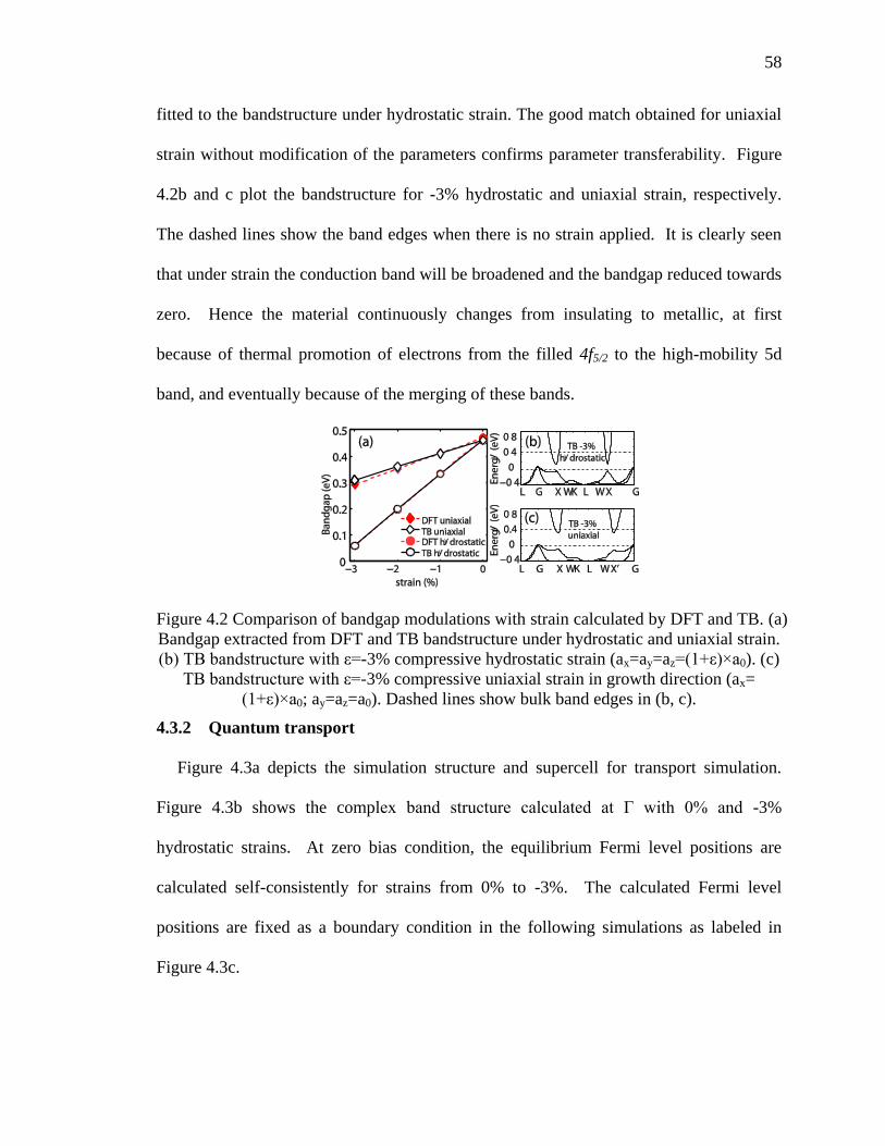
58
58
fitted to the bandstructure under hydrostatic strain. The good match obtained for uniaxial
strain without modification of the parameters confirms parameter transferability. Figure
4.2b and c plot the bandstructure for -3% hydrostatic and uniaxial strain, respectively.
The dashed lines show the band edges when there is no strain applied. It is clearly seen
that under strain the conduction band will be broadened and the bandgap reduced towards
zero. Hence the material continuously changes from insulating to metallic, at first
because of thermal promotion of electrons from the filled 4f5/2 to the high-mobility 5d
band, and eventually because of the merging of these bands.
Figure 4.2 Comparison of bandgap modulations with strain calculated by DFT and TB. (a)
Bandgap extracted from DFT and TB bandstructure under hydrostatic and uniaxial strain.
(b) TB bandstructure with ε=-3% compressive hydrostatic strain (ax=ay=az=(1+ε)×a0). (c)
TB bandstructure with ε=-3% compressive uniaxial strain in growth direction (ax=
(1+ε)×a0; ay=az=a0). Dashed lines show bulk band edges in (b, c).
4.3.2 Quantum transport
Figure 4.3a depicts the simulation structure and supercell for transport simulation.
Figure 4.3b shows the complex band structure calculated at Γ with 0% and -3%
hydrostatic strains. At zero bias condition, the equilibrium Fermi level positions are
calculated self-consistently for strains from 0% to -3%. The calculated Fermi level
positions are fixed as a boundary condition in the following simulations as labeled in
Figure 4.3c.

59
59
Figure 4.3 Transport simulation for SmSe with hydrostatic strain. (a) Simulated structure
in and 6nm channel super cell in transport simulation. (b) Real and imaginary band
structure for 0% and -3% hydrostatic strain. (c) Transmission with 0V and 0.05V linear
drop potential. (d) Vd=0.05V, spectral current, dJ/dE, with linear drop potential.
Current is calculated when 0.05V bias is applied to the drain contact which is assumed
to drop linearly along a 6nm SmSe channel (Figure 4.3a) via integration over the whole
Brillouin Zone with k-space spacing of 0.1π/a (a=0.62nm). Figure 4.3c shows the
transmission coefficient at Γ before and after applying bias. At zero bias, each
transmission step corresponds to a sub-band in Figure 4.3b.[61] When a linear drop
potential is applied, the values of transmission will not equal the numbers of incident
waves and the localized bands will no longer carry current due to the small band width.
For example, comparing the dashed and solid lines in Figure 4.3c, the transmission
diminishes at the top of the valence band and the transmission peak at E=-0.4eV becomes
a valley. Figure 3d plots the spectral current, dJ/dE, under the two strain conditions.[61,
69] The large variation in the spectral current with strain (> 103) indicates that a large
piezoresistive effect is still observed in the ballistic regime. After the same calculations
for 0% to -3% strain, ballistic resistances can be extracted. Ignoring the interference

60
60
effects between real contacts and channel, a change of resistance by 3 orders of
magnitude is obtained between -3% and 0% hydrostatic strain samples (0.075A/µm2 and
4.58×10⁻⁵
A/µm2). The exact value of the current requires accounting for the effect of the
electrodes, which we will leave for future studies.
The transport results in SmSe presented here are based on the band structure as
obtained from DFT calculations. At this level of sophistication the predicted band width
of the 4f valence band is of the order of 0.5 eV. As a result the top of the 4f valence bands
have relatively low hole masses allowing for the contributions to tunneling from modes
in the valence band. In contrast a much narrower width (of < 50 meV), suggesting strong
localization of the 4f states in SmX materials (X=S, Se, Te), can be deduced from data at
low temperatures. [70-72] Such localization (due to strong correlations which are not
properly be captured by DFT) would suppress tunneling via the valence band with the
increase of hole masses. Further experimental investigation is required to properly
characterize these material systems.
4.4 Summary and outlook
In this work, an ETB model accounting for second nearest neighbor coupling with full
sets of spdfs* orbitals has been developed to describe the band structure of rare-earth
chalcogenide SmSe. The parameterization captures the band structure obtained from
DFT and the effect of strain as obtained in DFT calculations. Calculations of the ballistic
current in nanoscale films within the NEGF formalism demonstrate that a large
piezoresistive effect is still observed in the ballistic regime. This work enables the
realistic modeling of piezoelectronic devices and serves as a valuable tool to optimize its
performance.

61
61
5. MULTIDIMENSIONAL SIMULATION ON CBRAM
5.1 Working principles of CBRAM
As shown in Table 1.2, Conductive bridging RAM (CBRAM)[73-75] as one of the
emerging memory technologies has advantages over the dominating flash memory on
high scalability, low power consumption, high resistance ratio and long retention.
CBRAM Utilizes the electrochemical formation and removal of metallic pathways in thin
films of solid electrode to get low and high resistances. CBRAM is based on redox
reaction of active electrode (Cu, Ag) and ion migration inside solid electrolyte (GeSe,
GeS, SiO2, TiO2) as shown in Figure 5.1. Electrolyte is insulating to electrons, but allows
metal ions to diffuse inside.
Copyright © 2005, IEEE
Figure 5.1 Principle of CBRAM. Directions of metal ion diffusion and electron
conduction. [73]
Figure 5.2 shows typical I-V characteristics of CBRAM. During the forming cycle,
active metal will dissolves into the solid electrolyte and forms metallic conductive

62
62
filaments. At anode Ag→Ag++e
-, ions are generated. Cation will swim towards cathode
and gain electron at cathode: Ag++e
-→Ag. Ag atoms will start to accumulate at cathode
and form filaments. Eventually, device will switch from high resistance to low resistance
when formation of filaments reaches anode. To help the forming process, metal clusters
could be doped prior to forming cycle in the electrolyte. Once the initial forming is
achieved, the filament will not be dissolved completely in following cycles. A much
smaller voltage is required to break the filament beginning from anode. The required
voltage to rebuild the filament should be smaller than the forming voltage as shown in
Figure 5.2.
However it is worth to mention that the process described in Figure 5.2(b) is not true
in nanoscale CBRAM cells in a recent simulation[76, 77]. There are two significant
differences: (1) The Cu ions will not deposit directly to the inactive electrode. Small
clusters of Cu atoms will be formed inside electrolyte and the clusters will make contact
with the inactive electrode. When the filament is formed, it will have a conical shape and
it is thicker at the active electrode, consistent with microscopy observations in larger cells.
(2) In nanoscale CBRAM cells, the filament after reset stage will dissolve into the
electrolyte quickly. A new filament will be formed, although the new filament is mostly
formed by atoms from the previously dissolved partial filament.

63
63
Figure 5.2 Typical IV characteristics of CBRAM showing bipolar asymmetric
programming/erase feature. [75] Reprinted from Microelectronic Enginnering, 88 (5),
pp814-816, Y. Bernard,V.T. Renard,P. Gonon,V. Jousseaume “Back-end-of-line
compatible Conductive Bridging RAM based on Cu and SiO2”(2011) with permission
from Elsevier.
5.2 Multi-scale, multi-physics simulation
Modeling this electrochemical process requires simulations in different physical
complexities. The filament formation has been simulated by molecular dynamics (MD)
with reactive potential ReaxFF [76, 78, 79], but quantum transport is prohibited due to
computational burden within density function theory (DFT). Empirical tight binding
(ETB) could handle quantum transport in structures of more realistic size by non-
equilibrium Green’s function (NEGF) calculations. Filaments at different stages in MD
will be taken as inputs for ETB calculations for ballistic conductance. For extremely
small devices containing a few hundred atoms, DFT-NEGF could even be used.
The conductance changes with respect to Morphologies of conducting filaments are
important for evaluating performance and reliability. Tunneling through electrolyte
before filament formation could be potentially harmful for achieving high resistance ratio.
Quantum simulations are important in predicting conductance changes in switching
process.

64
64
5.3 Methods
The electrochemical process modeling requires application of different physical
models in different scales. The filament formation is simulated by molecular dynamics
(MD) with the ReaxFF reactive force field [76, 78, 80]. Quantum transport is simulated
with non-equilibrium Green’s function [17].
The atom positions and the Mulliken charges calculated from charge equilibrium
calculation under external electrochemical potentials are taken from the MD simulations.
The charges are used to calculate the electrostatic potential with Poisson equation. The
atomic charge density is assumed to have a Gaussian distribution centered at atom.
Empirical Tight Binding Hamiltonian is constructed for an atomic configuration. The
simulation flow is shown in Figure 5.3.
The device is partitioned into slabs based on coupling with the Breadth-first search
method[81]. Such slab structure is suitable for transmission coefficient calculation with
the recursive Green’s function (RGF) technique. Because the charge self-consistent
calculation is not required at this stage, only forward RGF is performed. The self energy
is calculated with the Sancho-Rubio method[82].
The calculation is performed at Conte supercomputer. Each compute node is equipped
with two 8-core Intel Xeon-E5 processors and two 60-core Xeon Phi coprocessors. The
calculation is paralleled at each node with 2 MPI ranks and 8 OMP threads. The
computationally heavy matrix operations have been offloaded to Xeon Phi coprocessors
to gain maximum performance which gives speed up 3.2×. It takes roughly 800 seconds
to finish 1 energy point on 1 MPI rank.

65
65
Copyright © 2015, IEEE
Figure 5.3 Simulation flow. Structures and charge profiles are generated by MD
simulations. The electrostatic potential is calculated based on atomic charges. Current is
calculated by NEGF and conductance is extracted.
5.3.1 Molecular dynamics
For computer simulation of assemblies of molecules, two families of methods widely
used are Monte Carlo method (MC) [83] and molecular dynamics (MD)[84, 85]. MD
gives the dynamical properties of the system. Classical MD simulations treat molecules
as classical objects following the law of classical mechanics. The quantum MD considers
the quantum nature of chemical bond instead of “ball and stick” type model. However,
quantum MD for all valence electrons is still impractical for large systems.
The atomic force field which defines the forces between particles is important for
realistic MD simulation. Classical MD uses predefined potentials based on empirical data
or on independent structure calculations. The full interaction is broken up into two-body,
three-body and many-body contributions. Ab-initio MD could calculate the force “on-the-
fly” and consider electronic behavior from DFT, but it requires much higher
computational resources.

66
66
5.4 Material Parameterization and properties
5.4.1 Amorphous SiO2
Real electrolyte is made with amorphous SiO2, but parameterization of amorphous
material is difficult. Amorphous materials do not possess crystal structure, so there is no
dispersion, whereas dispersion is usually one of the most important targets in
parameterization and optimization.
When dealing with transport through SiO2 in literature within TB framework, it is
usually assume a well-defined crystallographic structure of SiO2 such as β-quartz,
tridymite or β-cristobalite[86-88] with up to 2nd
nearest neighbor coupling for oxygen
atoms. Otherwise fictitious SiO2 atom is assumed with first nearest neighbor sp3
description [89, 90].
There are a few researches on defects in amorphous SiO2 and they use empirical tight
binding [91, 92]. Their parameters mostly based on an early study conducted by Reilly
and Robertson [93, 94]. In these studies, they are not targeting on accurate matching
exact bandstructures rather they focus on qualitative understanding of effects of disorder
in amorphous SiO2. The distortion of bond length and bond angle has effects on onsite
and coupling parameters in TB. These effects are mostly considered through Harrison’s
rule of 1/d2 dependency and Slater-Koster table[18]. Effects of disorder on onsite
energies are considered through Madelung potential which is imposed on onsite energies
in [91].
In our study, Cu ions will diffuse inside amorphous SiO2 electrolyte. The whole
structure is generated through MD with ReaxFF[79]. Previous DFT and MD study [95,

67
67
96] shows the bond and angle distribution in α-SiO2 is not constant but follows certain
distribution like Table 5.1.
Several MD studies [97-99] have shown that the tetrahedral O-Si-O bond angle is
quite firm even in amorphous structures with 109.18o. Each oxygen is bonded to two
silicon atoms with Si-O-Si angle distributed from 120o to 180
o. The crystalline forms of
SiO2 are determined by the Si-O-Si angle.
Table 5.1 Short-range structural characteristics of glass samples. The average pair
distances are reported with standard deviation for the simulated values. [95]
Size Method Density(g/cm3) RSi-O RO-O RSi-Si
72 atoms
GGA 2.2 1.632(0.020) 2.67(0.104) 3.105(0.114)
LDA 2.2 1.621(0.022) 2.65(0.109) 3.100(0.113)
BKS 2.2 1.619(0.019) 2.64(0.119) 3.122(0.103)
BKS-NPT 2.33-2.52 1.609(0.018) 2.63(0.121) 3.059(0.108)
1479 atoms NVT 2.2 1.616(0.024) 2.64(0.116) 3.104(0.106)
NPT 2.33 1.609(0.024) 2.63(0.118) 3.072(0.111)
Figure 5.4 Bond length and bond angle in amorphous SiO2 generated by ReaxFF. (a)
Geometry of amorphous SiO2. (b-c) Distribution of bond length. (d-e) Distribution of
bond angle.

68
68
In our study, the amorphous SiO2 is generated by ReaxFF. As shown in Figure 5.4, the
calculated distribution is consistent with experiment and other simulations.
There has been comparison between GGA and LDA in SiO2 systems. Both methods
underestimate bandgap comparing to experimental values as shown in Table 5.2. Most of
the works conducted in literatures are done with LDA though.
Table 5.2 Bandgap for SiO2 obtained from ref. [98]. Most results based on LDA/GGA
will underestimate experimental bandgap (8.9eV for α-quartz)[100]. A study based on
Hatree-Fock over estimate bandgap significantly [101].
SiO2 Crystal Indirect Eg(eV) Direct Eg(eV)
α-quartz 5.785 6.073
α-cristobalite 5.525 5.525
β-cristobalite 5.317 5.317
Stishovite 5.606 5.606
Figure 5.5 Bandstructure for β-cristobalite obtained with parameters of O’Reilly and
Robertson[93]. This parameter set captures band position and could serve as initial values
for our TB parameterization.
Beginning with the initial value, fitting targets are summarized in Figure 5.6. The unit
cells and DFT bandstructure are shown for 4 different crystalline SiO2. For α-quartz, the
experimental bandgap is 8.9eV. The bandstructure is modified accordingly by scissor

69
69
operation during fitting. To keep consistency, the same scissor operation has been also
applied to all other crystalline SiO2.
Figure 5.6 Bandstructure for 4 different crystalline SiO2 calculated by LDA.
Figure 5.7 Copyright © 2015, IEEE. Comparison of bandstructure calculated by
optimized TB parameters and DFT. Two crystalline SiO2 are calculated by the same set
of parameters.
Figure 5.7 shows bandstructure of α-quartz and β-cristobalite. Both bandstructures
have been optimized and calculated with the same set of parameters. It is shown a

70
70
reasonable agreement is achieved for valence band. To fix the mismatch in higher
conduction bands it might require inclusion of orbital with higher energy.
5.4.2 Cu
After years of development, the Cu interconnection is finally compatible with the
Back-End-Of-Line (BEOL) of Si CMOS process. Therefore Cu is an ideal low cost
material for the anode of resistive memory embedded in Si integrated circuit. As a result,
Cu is chosen as active electrode in our study. Electrolyte could be SiO2 or Al2O3.
5.4.2.1 Confinement effects on Cu filaments
Shape of conduction filaments and tunneling between Cu clusters is the focus of this
study. Figure 5.8 shows positions of neighbors coupled to Cu atom determined by bond
radius which defines a sphere cut off boundary. In TB, atoms within the sphere are
coupled to the central atom.
Figure 5.8 Bond radius in TB determines number of neighbor atoms coupled.
For nanostructures, a 2NN parameterization is used for this work [27]. Figure 5.9
shows bandstructure calculated with the 2NN model for nanowire with different cross
sections.

71
71
Figure 5.9 Effects of confinement simulated with environmental dependent TB with 2nd
nearest neighbor model. [27]
Figure 5.10 shows comparison of bandstructures for Cu nanowire calculated by DFT
with ATK and TB with NEMO5. Transmission calculated by QTBM matches with
dispersion. It is shown although bulk bandstructures simulated with two methods match
very well, parameters still needs to be optimized for nanostructures under confinement.
However, the bandstructures near Fermi level are matching well, which means this TB
parameterization is good for qualitatively predicting Cu nanowire conductance.
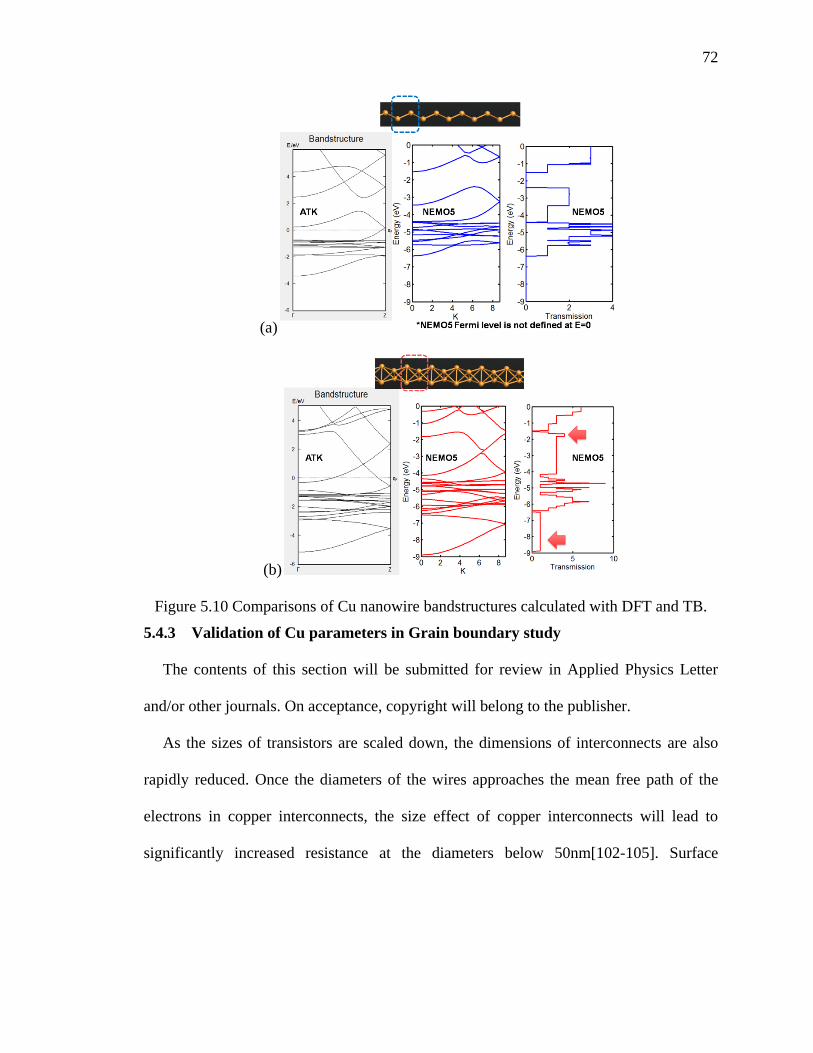
72
72
(a)
(b)
Figure 5.10 Comparisons of Cu nanowire bandstructures calculated with DFT and TB.
5.4.3 Validation of Cu parameters in Grain boundary study
The contents of this section will be submitted for review in Applied Physics Letter
and/or other journals. On acceptance, copyright will belong to the publisher.
As the sizes of transistors are scaled down, the dimensions of interconnects are also
rapidly reduced. Once the diameters of the wires approaches the mean free path of the
electrons in copper interconnects, the size effect of copper interconnects will lead to
significantly increased resistance at the diameters below 50nm[102-105]. Surface
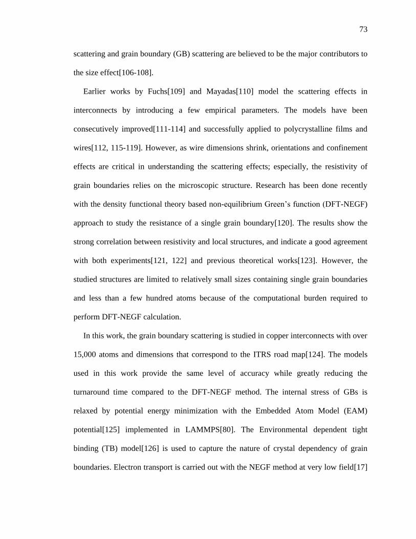
73
73
scattering and grain boundary (GB) scattering are believed to be the major contributors to
the size effect[106-108].
Earlier works by Fuchs[109] and Mayadas[110] model the scattering effects in
interconnects by introducing a few empirical parameters. The models have been
consecutively improved[111-114] and successfully applied to polycrystalline films and
wires[112, 115-119]. However, as wire dimensions shrink, orientations and confinement
effects are critical in understanding the scattering effects; especially, the resistivity of
grain boundaries relies on the microscopic structure. Research has been done recently
with the density functional theory based non-equilibrium Green’s function (DFT-NEGF)
approach to study the resistance of a single grain boundary[120]. The results show the
strong correlation between resistivity and local structures, and indicate a good agreement
with both experiments[121, 122] and previous theoretical works[123]. However, the
studied structures are limited to relatively small sizes containing single grain boundaries
and less than a few hundred atoms because of the computational burden required to
perform DFT-NEGF calculation.
In this work, the grain boundary scattering is studied in copper interconnects with over
15,000 atoms and dimensions that correspond to the ITRS road map[124]. The models
used in this work provide the same level of accuracy while greatly reducing the
turnaround time compared to the DFT-NEGF method. The internal stress of GBs is
relaxed by potential energy minimization with the Embedded Atom Model (EAM)
potential[125] implemented in LAMMPS[80]. The Environmental dependent tight
binding (TB) model[126] is used to capture the nature of crystal dependency of grain
boundaries. Electron transport is carried out with the NEGF method at very low field[17]

74
74
and electronic resistivity is extracted by the Landauer formula. At finite temperature, the
conductance is
where Tn is the transmission function for
subband n.
The resistivities of geometries containing single grain boundaries are first calculated
and compared with the DFT-NEGF method[120] and the Extended Hückel (EHT)
model[127]. Single grain boundaries, also known as coherent grain boundaries[120, 128,
129], have shown high rates of appearance in real interconnects because of the low
interface energy. Figure 5.11a shows a Ʃ5 coherent GB following the notation of
Coincidence Site Lattice (CSL). The coherent grain boundary structures are generated
with GBSTUDIO[130]. The lattice constant of 0.3615nm is used which is calculated by
potential energy minimization with the EAM potential[125] and the value matches with
experiment[131]. The structure is then relaxed. Only N layers of atoms from the
boundary layer are relaxed while all other layers are fixed as illustrated in Figure 5.11a. It
is found that beyond N=3, the total energies no longer change significantly as shown in
Figure 5.11(b-d) for three different twin GBs. This result shows the same trend as
predicted by ab inito approach[120].
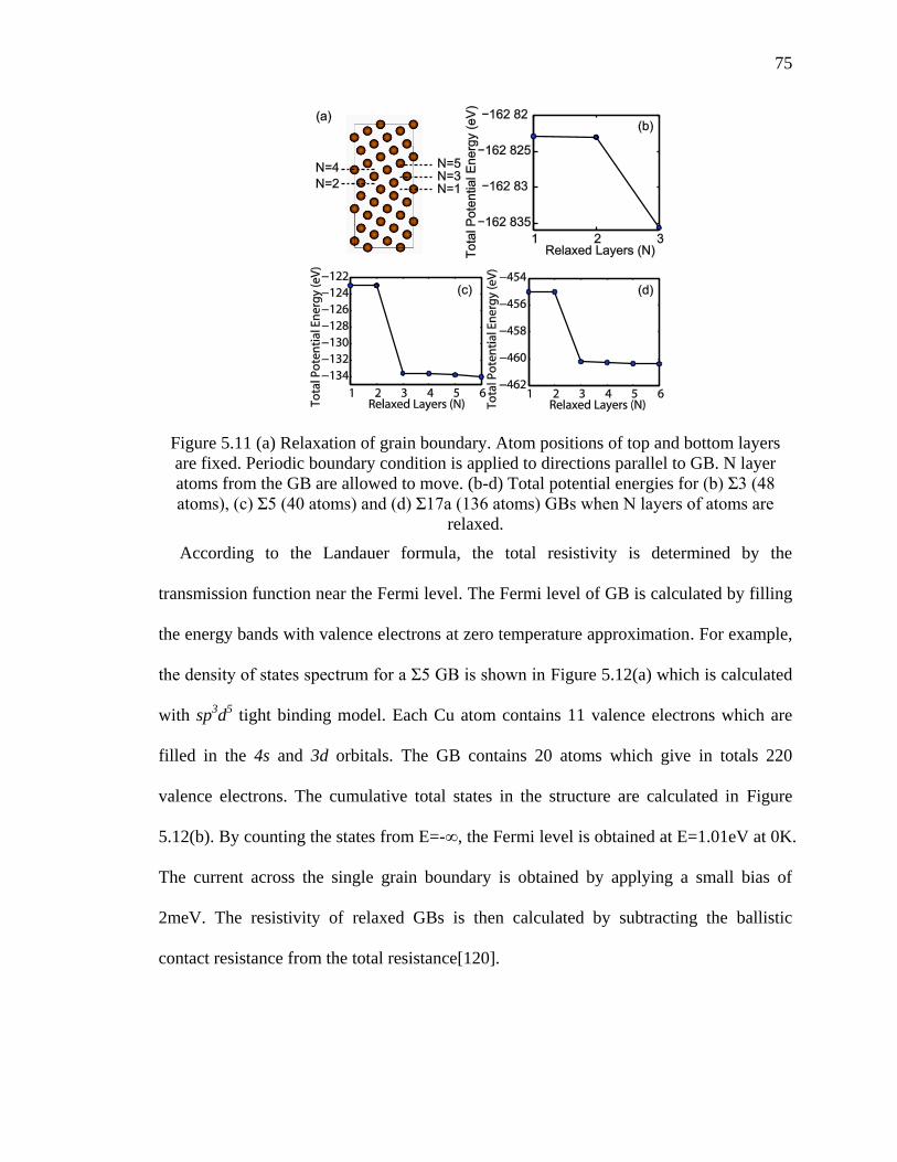
75
75
Figure 5.11 (a) Relaxation of grain boundary. Atom positions of top and bottom layers
are fixed. Periodic boundary condition is applied to directions parallel to GB. N layer
atoms from the GB are allowed to move. (b-d) Total potential energies for (b) Ʃ3 (48
atoms), (c) Ʃ5 (40 atoms) and (d) Ʃ17a (136 atoms) GBs when N layers of atoms are
relaxed.
According to the Landauer formula, the total resistivity is determined by the
transmission function near the Fermi level. The Fermi level of GB is calculated by filling
the energy bands with valence electrons at zero temperature approximation. For example,
the density of states spectrum for a Ʃ5 GB is shown in Figure 5.12(a) which is calculated
with sp3d
5 tight binding model. Each Cu atom contains 11 valence electrons which are
filled in the 4s and 3d orbitals. The GB contains 20 atoms which give in totals 220
valence electrons. The cumulative total states in the structure are calculated in Figure
5.12(b). By counting the states from E=-∞, the Fermi level is obtained at E=1.01eV at 0K.
The current across the single grain boundary is obtained by applying a small bias of
2meV. The resistivity of relaxed GBs is then calculated by subtracting the ballistic
contact resistance from the total resistance[120].

76
76
Figure 5.12 Extract Fermi level from density calculation. (a) Density of states spectrum.
(b) Cumulative total electron states.
6 types of coherent GBs are calculated and the results are summarized in Table 5.3. It
is shown that the TB results match well with NEGF-DFT and available experimental
values. It shows better trend than the EHT model. Even with the similar accuracy, the TB
model is more efficient because it has smaller interaction radius and it does not require
the evaluation of overlapping matrix.
Table 5.3 Resistivity calculated by DFT from Ref. [120] and by 2nd
nearest neighbor TB
and 3rd
nearest neighbor EHT models in this work.
Resistivity (10-12
Ω-cm2)
DFT(exp.)[120] ETB 2NN EHT 3NN
Ʃ3 0.158 / 0.148 / 0.155 / 0.202 (0.17) 0.116 0.248
Ʃ5 1.49 / 1.885 1.28 0.997
Ʃ9 1.75 1.49 1.008
Ʃ11 0.75 0.715 0.574
Ʃ13a 2.41 2.272 1.368
Ʃ17a 2.01 1.916 1.15
The TB model is then applied to study the effects of random grain boundaries in
copper interconnect. The primary transport orientation of the interconnects is fixed at
[110] direction, which gives the highest conductance. This is also confirmed by the
previous study[126].

77
77
Starting from a homogeneous [110] oriented structure, the multi-GB geometry is
created according to the following steps: (1) Generate scattered grain seeds. (2) Create
Voronoi diagram with Qhull.[132] (3) Divide the atomistic domain into grains according
to the Voronoi diagram. (4) Determine rotation angles for each grain. (5) Geometry
relaxation. The process is outlined in Figure 5.13a for a 2D structure.
Figure 5.13 Geometry generation. (a) Generate random seed → Voronoi diagram →
Divide original geometry into grains. (b) Simulation domain with leads attached.
According to the directions of the GBs along the transport direction, the structures are
categorized into two classes. If the neighboring GBs are aligned in parallel, it is called
“bamboo” structures. Otherwise the GBs are distributed in random patterns. Both
geometries are shown in Figure 5.14a.
The crystal orientations of neighboring GBs are different by a misorientation angle θ.
In general cases, if the misorientation θ is less than 15 degree, it is known as low angle
grain boundary (LAGB)[133]; if the misorientation is more than 15 degree, it is called
high angle grain boundary (HAGB). The orientations of the GBs as well as the
misorientation angles both have big effects on the resistance of interconnect.
To study the effects of the misorientation angle, the GBs are idealized into two groups.
The first group is “tilt” GBs. As shown in Figure 5.14b, the tilt GB is formed by a

78
78
rotation axis parallel to the GB plane. The second group is “twist” GBs. As shown in
Figure 5.14c the twist GB is formed by a rotation axis vertical to the GB plane.
Figure 5.14 Definition of special grain boundaries. (a) Bamboo and random GBs. (b) Tilt
and twist GBs.
The tile GBs are simulated with 2D geometries as shown in Figure 5.14b. The
“bamboo” structure is constructed with 3 grains (W=5nm and L=10nm). The middle
grain is rotated by θ = 0 to 45 degrees. The twist GBs are simulated with 3D nanowire
geometries as shown in Figure 5.13c. Three grains are constructed with T=W=3nm,
L=5nm. The middle grain is rotated by θ = 0 to 90 degrees. The calculated resistance is
shown inFigure 5.15. The twist GB resistances are normalized by T=3nm.
Figure 5.15 Resistance of (a) tilt and (b) twist GBs.

79
79
From Figure 5.15, it is shown that the LAGBs in general have smaller resistance than
HAGBs. This is due to fewer defects at LAGBs.
The tilt and twist GBs are idealized conditions. Real GBs contain both in-plane and
out-of-plane rotations. To study general rotation conditions, total of 31 3D structures are
constructed with both “tilt” and “twist” rotations including 15 bamboo structures and 16
random structures with 2 to 5 grains. In this study, the “tilt” and “twist” rotation angles
are limited to -15 to 15 degrees. The results are summarized in Figure 5.16.
Figure 5.16 (a) Resistance of GBs with general rotations. (b) Voronoi diagram for
random GBs with 4 grains. (c) Voronoi diagram for bamboo GBs with 4 grains.
From Figure 5.16a, it is shown that with the same number of grains, “bamboo”
structure does not necessary provide lower resistance. This could be explained from
Figure 5.16b,c. With random GB configurations, carriers usually go through less GBs
from one lead to the other. With more grains, the average resistance will increase. The
wide distribution of resistances shows that the dominating factor is the orientation of GBs
rather than the number of grains.
In summary, the interconnect resistances with the coherent single grain boundary and
random grain boundaries are studied with the environment - dependent tight binding
model. The proposed simulation models are efficient and suitable to study more realistic

80
80
geometries. The accuracy of the model is validated against the DFT and the EHT models.
Some representative GB geometries are studied. The GB orientations and misorientation
angles both show big impacts on the GB resistance. With more samples, a statistical
model could be generated for compact modeling purposes. This study could be easily
coupled to lattice dynamic simulations for other types of defects in the metal interconnect.
5.4.4 Cu oxides
Study of metal contact is critical for understanding of device performance. Most
studies treated the barrier in phenomenological way [134, 135]. In this work, the metal-
semiconductor and metal-insulator (electrolyte) interface will be constructed
atomistically and this study will be composed of two parts.
Morphology at the interface will be studied at first. This study will be carried out by
DFT and MD with ReaxFF. Then the interface coupling will be parameterized. Currently,
we propose that a transferable TB parameter set should be able to reproduce multiple Cu
oxide crystals as CuO, Cu2O which are common oxidized status for Cu in the Cu-SiO2
interface. Our preliminary study shows that normal LDA and GGA could not reproduce
Cu oxide bandgap correctly. For Cu2O, only Hybrid functional could give close bandgap
to experiments as shown in Figure 5.17. For CuO and Cu4O3, LDA+U could reproduce
bandgap accurately according to [136].

81
81
Figure 5.17 Bandstructure of Cu2O simulated with GGA and Hybrid functional (VASP
results calculated by Yaohua Tan). Only Hybrid functional result shows bandgap close to
experimental value. [136]
We have conducted calculations on Cu2O and CuO with LDA+U[137]. Cu2O has a
simple cubic crystal structure, whereas CuO has structure of monoclinic. Primitive cells
are shown in Figure 5.18a-b. However, because CuO has an unpaired electron in d-orbital,
the antiferromagnetic unit cell is twice of the size of the primitive cell. For all simulations,
U=7.5eV and J=0.98eV are adopted from [65]. These value has been adopted in several
studies, though there is also study testing U-J over a wide range for a optimal value [138].
In the same work, the bandgap of CuO is found more sensitive to value of U while Cu2O
is less affected. Decomposition of PDOS shows that this is because in Cu2O the valence
band is mixture of Cu 3d, O 2p and Cu 4s and conduction band is mixture of Cu 3d, O 3s
and Cu 4s. Since LDA+U affects only the localized d orbital, it is not efficient in Cu2O.
This has been confirmed by our preliminary results.

82
82
Figure 5.18 Crystal structure constructed from ATK builder. (a) Primitive unit cell of
Cu2O. (b) Primitive unit cell of CuO. (c) Antiferromagnetic unit cell for CuO. Thick
arrows indicate orientations of local magnetic moments. Thin arrows along [011]
direction shows atom chain with strongest superexchange.
Figure 5.19 shows our preliminary DFT calculation results from ATK and ELK
(http://elk.sourceforge.net/). We note that although the crystal structures of Cu2O and
CuO are clear. The equilibrium lattice constants are ambiguous in literatures. Various
values have been provided both from experiments and DFT calculations [138-142]. Our
preliminary simulations simply take value from Wyckoff [143]. The geometry should be
optimized later with respect to total energy. The lattice constant should have impact on
the final bandgap.

83
83
Figure 5.19 Bandstructure of Cu2O calculated with (a) ATK with LDA+U (b) ELK with
LDA+U compare to ref [136] with HSE. Results of (b) is calculated with crystal structure
from Wyckoff [143] with 11×11×11 k point and plane wave cut-off roughly 400eV.
In Figure 5.19, ATK and ELK give very close bandgap. The value is not quite
different from Figure 5.17a-b, which are LDA/GGA calculation without U. HSE provides
a much better match with experiments.
Figure 5.20 Comparison of bandstructure calculated by HSE (HSE06 in VASP) and
LDA+U (ELK). Bandstructure of LDA+U has been modified with scissor operation to
match band gap with HSE.
In Figure 5.20, bandstructure of LDA+U has been shifted with scissor operation to
match the bandgap of HSE. Although HSE and LDA+U give different bandgap, the

84
84
effective masses for the lowest conduction band and valence band are very similar. To
reduce computational burden, the LDA+U results with scissor operation will be used as
fitting target in this work.
Figure 5.21 shows the density of states for Cu2O. Interstitial DOS implies coupling of
neighbor atoms outside the muffin-tin radius, while the localized DOS shows a strong
localized orbital. In Cu2O, the localized orbital is d-orbital in Cu atoms. Decompositions
of contributions by atom and orbital in Figure 5.21 show the main contributions from O
atom are s- and p-orbital. The main contributions from Cu atom are s-, p- and d-orbital.
As a result, TB model of sp3d
5 is used for fitting.
Figure 5.21 Density of state for Cu2O and contributions of O and Cu atom to each band.
Figure 5.22 shows the unit cell of Cu2O. Two unit cells are shown here to demonstrate
coupling of atoms up to 4th
nearest neighbor. In our model, coupling of Cu-O(I), Cu-Cu
and Cu-O(II) are included. The comparison of the initial TB results and DFT is also
shown in Figure 5.22.
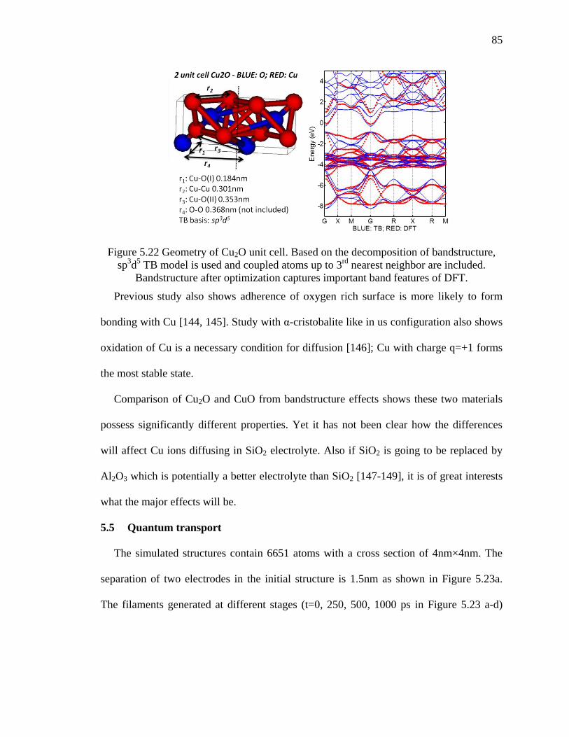
85
85
Figure 5.22 Geometry of Cu2O unit cell. Based on the decomposition of bandstructure,
sp3d
5 TB model is used and coupled atoms up to 3
rd nearest neighbor are included.
Bandstructure after optimization captures important band features of DFT.
Previous study also shows adherence of oxygen rich surface is more likely to form
bonding with Cu [144, 145]. Study with α-cristobalite like in us configuration also shows
oxidation of Cu is a necessary condition for diffusion [146]; Cu with charge q=+1 forms
the most stable state.
Comparison of Cu2O and CuO from bandstructure effects shows these two materials
possess significantly different properties. Yet it has not been clear how the differences
will affect Cu ions diffusing in SiO2 electrolyte. Also if SiO2 is going to be replaced by
Al2O3 which is potentially a better electrolyte than SiO2 [147-149], it is of great interests
what the major effects will be.
5.5 Quantum transport
The simulated structures contain 6651 atoms with a cross section of 4nm×4nm. The
separation of two electrodes in the initial structure is 1.5nm as shown in Figure 5.23a.
The filaments generated at different stages (t=0, 250, 500, 1000 ps in Figure 5.23 a-d)

86
86
from MD are taken as inputs for the ETB calculations for ballistic conductance. The time
step for MD simulations is 0.5fs.
With the generated structures, current through the devices are calculated at Vd=-1V.
Figure 5.24 shows the calculated current at different times at Vd=-1V and the
transmission coefficient at t=0ps and 250ps. It is shown as soon as the Cu atoms start to
form clusters inside SiO2, the current increases. Current ratio of I(t0=0ps)/I(t1=250ps) =
195 is obtained. When more filaments are constructed, the resistance is lowered and the
current will keep increasing.
Figure 5.23 Copyright © 2015, IEEE. Diffusion of Cu atoms in SiO2 at t=0, 250, 500,
1000ps. Si and O atoms are not plotted for better visibility. (a) Distance between
electrodes is 1.5nm in initial structure. (b) Clusters are formed in SiO2. Two electrodes
are not connected by filaments. (c) Two electrodes are connected by Cu filaments. The
connectivity is plotted based on a coupling radius of 0.39nm. (d) More filaments are
formed.
Figure 5.24 Copyright © 2015, IEEE. (a) Current for structures at Fig.3 at Vd=-1V. (b)
Total transmission at t=0ps and t=250ps.
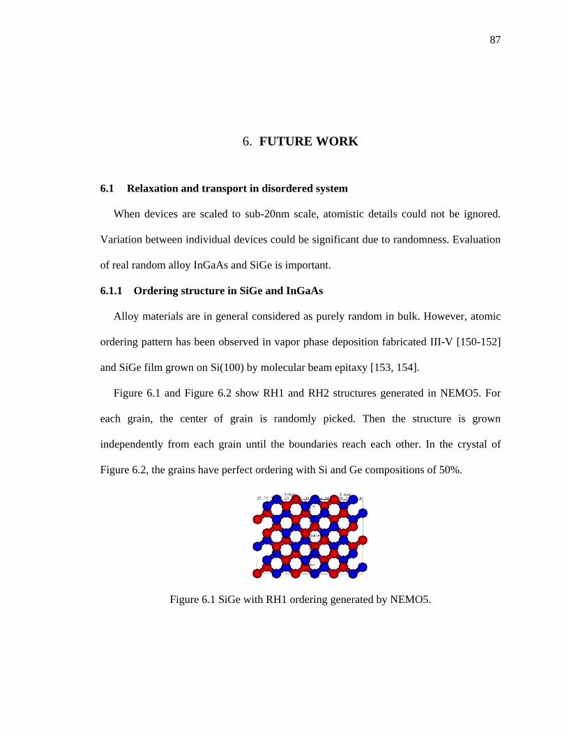
87
87
6. FUTURE WORK
6.1 Relaxation and transport in disordered system
When devices are scaled to sub-20nm scale, atomistic details could not be ignored.
Variation between individual devices could be significant due to randomness. Evaluation
of real random alloy InGaAs and SiGe is important.
6.1.1 Ordering structure in SiGe and InGaAs
Alloy materials are in general considered as purely random in bulk. However, atomic
ordering pattern has been observed in vapor phase deposition fabricated III-V [150-152]
and SiGe film grown on Si(100) by molecular beam epitaxy [153, 154].
Figure 6.1 and Figure 6.2 show RH1 and RH2 structures generated in NEMO5. For
each grain, the center of grain is randomly picked. Then the structure is grown
independently from each grain until the boundaries reach each other. In the crystal of
Figure 6.2, the grains have perfect ordering with Si and Ge compositions of 50%.
Figure 6.1 SiGe with RH1 ordering generated by NEMO5.

88
88
(a) (b)
Figure 6.2 Grains of SiGe with different ordering directions in RH2 ordering. (a) Each
color shows a grain with uniform ordering direction. (b) SiGe with RH2 ordering.
Figure 6.3 shows SixGe1-x with different Si compositions. The process of building
these crystals is listed below:
Build perfect Si crystal.
Generate random grain centers. Choose equivalent ordering direction for each
grain and grow all grains independently.
Generate disorder inside ordering geometry. Take out N Si atoms and replace
them with Ge. Take out the same amount of Ge atoms and replace them with
Si. N is determined by input option degree of ordering.
Randomly replace Si or Ge atoms to preserve desired SixGe1-x composition.
It could be shown, even with 50% Si atoms, the crystal is not perfect ordered due to
defined degree of ordering.
This short range ordering near surface could be important since the charge is
usually confined in the triangular potential well near surface. The challenges of this
study will be how to connect the simulated structure to realistic devices which requires
experimental input or advanced process modeling.

89
89
(a) (b) (c)
Figure 6.3 SixGe1-x with x=0.2, 0.5, 0.8. Each chunk with 2 grains with degree of
ordering=0.9. Ordering direction are (1,1,1) (-1,-1,1) (-1,1,-1) (1,-1,-1) with probabilities
(0.2609, 0.3043, 0.2174, 0.2174)
6.2 Validation of the Modeling Approach for CBRAM
The flow for simulation has been presented in chapter 5. The initial parameterization
for SiO2 and Cu has been validated and applied to realistic devices. Before applying the
modeling approach to realistic devices, firstly the validation of the simulations should be
performed.
Empirical tight binding provides the possibility to simulation large scale devices,
while the accuracy should be tested in smaller devices. For small devices, it is possible to
perform DFT based NEGF simulations. The obtained results should be consistent with
TB.
Secondly, the EHT model could be applied to the CBRAM. The advantages of the
EHT model in CBRAM simulation is the dealing of the interface. The EHT model does
not require the fitting of special parameters for the interface bonding. However, fitting of
bulk parameters are still required and the transferability is not always guaranteed.

LIST OF REFERENCES

90
90
LIST OF REFERENCES
[1] J. A. Del Alamo, "Nanometre-scale electronics with III-V compound
semiconductors," Nature, vol. 479, pp. 317-323, 2011.
[2] S. R. Mehrotra, et al., "Simulation Study of Thin-Body Ballistic n-MOSFETs
Involving Transport in Mixed Γ-L Valleys," Electron Device Letters, IEEE,
vol.34, no.9, pp.1196-1198, 2013.
[3] S. Takagi, et al., "Device structures and carrier transport properties of advanced
CMOS using high mobility channels," Solid-State Electronics, vol. 51, pp. 526-
536, 2007.
[4] S. Kim, et al., "Strained extremely-thin body In 0.53 Ga 0.47 As-on-insulator
MOSFETs on Si substrates," in VLSI Technology (VLSIT), 2013 Symposium on,
2013, pp. T50-T51.
[5] R. C. Bowen, et al., "Quantitative simulation of a resonant tunneling diode,"
Journal of Applied Physics, vol. 81, pp. 3207-3213, 1997.
[6] S. Sze, "Physics of semiconductor devices. 1981," ed: Wiley, New York, 1981.
[7] A. C. Seabaugh and Q. Zhang, "Low-voltage tunnel transistors for beyond CMOS
logic," Proceedings of the IEEE, vol. 98, pp. 2095-2110, 2010.
[8] Z. Jiang, et al., "Empirical Tight-binding Parameterization of SmSe in the
sp3d5f7s* model," in https://nanohub.org/resources/17369, ed, 2013.
[9] D. M. Newns, et al., "High Response Piezoelectric and Piezoresistive Materials
for Fast, Low Voltage Switching: Simulation and Theory of Transduction Physics
at the Nanometer‐Scale," Advanced Materials, 2012.
[10] D. Newns, et al., "The piezoelectronic transistor: A nanoactuator-based post-
CMOS digital switch with high speed and low power," MRS Bulletin, vol. 37, pp.
1071-1076, 2012.
[11] A. Jayaraman, et al., "Continuous and Discontinuous Semiconductor-Metal
Transition in Samarium Monochalcogenides Under Pressure," Physical Review
Letters, vol. 25, pp. 1430-1433, 1970.
[12] P. Hohenberg and W. Kohn, "Inhomogeneous electron gas," Physical Review, vol.
136, p. B864, 1964.
[13] W. Kohn and L. J. Sham, "Self-consistent equations including exchange and
correlation effects," Physical Review, vol. 140, p. A1133, 1965.
[14] L. Nordstrom and D. J. Singh, "Planewaves, Pseudopotentials, and the LAPW
method" Springer Science & Business Media, 2006.
[15] G. Klimeck, et al., "Atomistic simulation of realistically sized nanodevices using
NEMO 3-D - Part I: Models and benchmarks," IEEE Transactions on Electron
Devices, vol. 54, pp. 2079-2089, 2007.
91
91
[16] G. Klimeck and M. Luisier, "Atomistic modeling of realistically extended
semiconductor devices with NEMO and OMEN," Computing in Science &
Engineering, vol. 12, pp. 28-35, 2010.
[17] S. Steiger, et al., "NEMO5: a parallel multiscale nanoelectronics modeling tool,"
IEEE Trans on Nano, vol. 10, 2011.
[18] J. C. Slater and G. Koster, "Simplified LCAO method for the periodic potential
problem," Physical Review, vol. 94, pp. 1498, 1954.
[19] F. Bloch, "Quantum mechanics of electrons in crystal lattices," Z. Phys, vol. 52,
pp. 555-600, 1928.
[20] T. B. Boykin, et al., "Valence band effective-mass expressions in the sp(3)d(5)s(*)
empirical tight-binding model applied to a Si and Ge parametrization," Physical
Review B, vol. 69, 2004.
[21] G. Klimeck, et al., "sp3s* Tight-binding parameters for transport simulations in
compound semiconductors," Superlattices and Microstructures, vol. 27, pp. 519-
524, 2000.
[22] T. B. Boykin, et al., "Diagonal parameter shifts due to nearest-neighbor
displacements in empirical tight-binding theory," Physical Review B, vol. 66, p.
125207, 2002.
[23] J.-M. Jancu, et al., "Empirical spds* tight-binding calculation for cubic
semiconductors: General method and material parameters," Physical Review B,
vol. 57, p. 6493, 1998.
[24] R. E. Cohen, et al., "Tight-binding total-energy method for transition and noble
metals," Physical Review B, vol. 50, p. 14694, 1994.
[25] M. J. Mehl and D. A. Papaconstantopoulos, "Applications of a tight-binding total-
energy method for transition and noble metals: Elastic constants, vacancies, and
surfaces of monatomic metals," Physical Review B, vol. 54, p. 4519, 1996.
[26] Y. Tan, et al., "Empirical tight binding parameters for GaAs and MgO with
explicit basis through DFT mapping," Journal of Computational Electronics, pp.
1-5, 2013.
[27] G. Hegde, et al., "An Environment-dependent Semi-Empirical Tight Binding
Model Suitable for Electron Transport in Bulk Metals, Metal Alloys, Metallic
Interfaces and Metallic Nanostructures I-Model and Validation," arXiv preprint
arXiv:1311.6082, 2013.
[28] Y. Q. Wu, et al., "0.8-V Supply Voltage Deep-Submicrometer Inversion-Mode
In0.75Ga0.25As MOSFET," Electron Device Letters, IEEE, vol. 30, pp. 700-702,
2009.
[29] P. Seung Hyun, et al., "Performance Comparisons of III-V and Strained-Si in
Planar FETs and Nonplanar FinFETs at Ultrashort Gate Length (12 nm),"
Electron Devices, IEEE Transactions on, vol. 59, pp. 2107-2114, 2012.
[30] M. Radosavljevic, et al., "Non-planar, multi-gate InGaAs quantum well field
effect transistors with high-κ gate dielectric and ultra-scaled gate-to-drain/gate-to-
source separation for low power logic applications," in Electron Devices Meeting
(IEDM), 2010 IEEE International, pp. 6.1. 1-6.1. 4, 2010

92
92
[31] A. Paul, et al., "Performance Prediction of Ultrascaled SiGe/Si Core/Shell
Electron and Hole Nanowire MOSFETs," IEEE Electron Device Letters, vol. 31,
pp. 278-280, 2010.
[32] Z. Jiang, et al., "Effects of interface disorder on valley splitting in SiGe/Si/SiGe
quantum wells," Applied Physics Letters, vol. 100, p. 103502, 2012.
[33] S. R. Mehrotra, et al., "Atomistic approach to alloy scattering in Si1− xGex,"
Applied Physics Letters, vol. 98, p. 173503, 2011.
[34] M. Luisier, "Performance comparison of GaSb, strained-Si, and InGaAs double-
gate ultrathin-body n-FETs," Electron Device Letters, IEEE, vol. 32, pp. 1686-
1688, 2011.
[35] M. Lundstrom, Fundamentals of carrier transport, 2nd ed. Cambridge, U.K. ;
New York: Cambridge University Press, 2000.
[36] M. V. Fischetti, et al., "Theoretical study of some physical aspects of electronic
transport in nMOSFETs at the 10-nm gate-length," Electron Devices, IEEE
Transactions on, vol. 54, pp. 2116-2136, 2007.
[37] N. Neophytou, et al., "Performance analysis of 60-nm gate-length III–V InGaAs
HEMTs: Simulations versus experiments," Electron Devices, IEEE Transactions
on, vol. 56, pp. 1377-1387, 2009.
[38] Y. He, et al., "Non-equilibrium Green's functions method: Non-trivial and
disordered leads," Applied Physics Letters, vol. 105, p. 213502, 2014.
[39] S. Mookerjea, et al., "Experimental demonstration of 100nm channel length In
0.53 Ga 0.47 As-based vertical inter-band tunnel field effect transistors (TFETs)
for ultra low-power logic and SRAM applications," in Electron Devices Meeting
(IEDM), 2009 IEEE International, 2009, pp. 1-3.
[40] F. Mayer, et al., "Impact of SOI, Si 1-x Ge x OI and GeOI substrates on CMOS
compatible tunnel FET performance," in Electron Devices Meeting, 2008. IEDM
2008. IEEE International, 2008, pp. 1-5.
[41] D. Leonelli, et al., "Performance enhancement in multi gate tunneling field effect
transistors by scaling the fin-width," Japanese Journal of Applied Physics, vol. 49,
p. 04DC10, 2010.
[42] Y. Lu, et al., "DNA functionalization of carbon nanotubes for ultrathin atomic
layer deposition of high κ dielectrics for nanotube transistors with 60 mv/decade
switching," Journal of the American Chemical Society, vol. 128, pp. 3518-3519,
2006.
[43] W. Y. Choi, et al., "Tunneling field-effect transistors (TFETs) with subthreshold
swing (SS) less than 60 mV/dec," Electron Device Letters, IEEE, vol. 28, pp. 743-
745, 2007.
[44] J. Appenzeller, et al., "Band-to-band tunneling in carbon nanotube field-effect
transistors," Physical Review Letters, vol. 93, p. 196805, 2004.
[45] T. Krishnamohan, et al., "Double-Gate Strained-Ge Heterostructure Tunneling
FET (TFET) With record high drive currents and << 60mV/dec subthreshold
slope," in Electron Devices Meeting, 2008. IEDM 2008. IEEE International, 2008,
pp. 1-3.
[46] S. H. Kim, et al., "Germanium-source tunnel field effect transistors with record
high I ON/I OFF," in VLSI Technology, 2009 Symposium on, 2009, pp. 178-179.

93
93
[47] C. H. Jan, et al., "A 32nm SoC platform technology with 2<sup>nd</sup>
generation high-k/metal gate transistors optimized for ultra low power, high
performance, and high density product applications," in Electron Devices Meeting
(IEDM), 2009 IEEE International, pp. 1-4, 2009
[48] G. Zhou, et al., "Novel gate-recessed vertical InAs/GaSb TFETs with record high
ION of 180 μA/μm at VDS= 0.5 V." Electron Devices Meeting (IEDM), 2012
IEEE International, pp.32.6.1-32.6.4, 10-13 Dec. 2012
[49] R. Li, et al., "InAs/AlGaSb heterojunction tunnel field‚Äêeffect transistor with
tunnelling in‚Äêline with the gate field," Physica Status Solidi (c), 2012.
[50] Sentaurus Device User Guide, E-2010.12 ed., 2010.
[51] Y. Lu, et al., "Performance of AlGaSb/InAs TFETs With Gate Electric Field and
Tunneling Direction Aligned," Electron Device Letters, IEEE , vol.33, no.5,
pp.655-657, May 2012
[52] M. Luisier and G. Klimeck, "Simulation of nanowire tunneling transistors: From
the Wentzel–Kramers–Brillouin approximation to full-band phonon-assisted
tunneling," Journal of Applied Physics, 107, 084507, 2010
[53] A. W. Dey, et al., "Single InAs/GaSb Nanowire Low-Power CMOS Inverter,"
Nano Letters, vol. 12, pp. 5593-5597, 2012/11/14 2012.
[54] T. N. Theis and P. M. Solomon, "It’s time to reinvent the transistor!," Science, vol.
327, pp. 1600-1601, 2010.
[55] M. Imada, et al., "Metal-insulator transitions," Reviews of Modern Physics, vol.
70, p. 1039, 1998.
[56] N. Mott, "Metal-insulator transition," Reviews of Modern Physics, vol. 40, pp.
677-683, 1968.
[57] M. Copel, P. M. Solomon and T.M. Shaw (private communication).
[58] A. Jayaraman, et al., "Pressure-volume relationship and pressure-induced
electronic and structural transformations in Eu and Yb monochalcogenides,"
Physical Review B, vol. 9, pp. 2513-2520, 1974.
[59] V. N. Antonov, et al., "Electronic structure of mixed-valence semiconductors in
the LSDA+U approximation. I. Sm monochalcogenides," Physical Review B, vol.
66, p. 165208, 2002.
[60] T. B. Boykin, et al., "Diagonal parameter shifts due to nearest-neighbor
displacements in empirical tight-binding theory," Physical Review B, vol. 66,
2002.
[61] M. Luisier, et al., "Atomistic simulation of nanowires in the sp3d3s* tight-binding
formalism: From boundary conditions to strain calculations," Physical Review B,
vol. 74, p. 205323, 2006.
[62] P. O. Löwdin, "On the Non-Orthogonality Problem Connected with the Use of
Atomic Wave Functions in the Theory of Molecules and Crystals," The Journal of
Chemical Physics, vol. 18, p. 365, 1950.
[63] See supplementary material at http://dx.doi.org/10.1063/1.4804601 for list of ETB
paremeters of SmSe.
[64] Y. Zhang and W. Yang, "Comment on “Generalized Gradient Approximation
Made Simple”," Physical Review Letters, vol. 80, pp. 890-890, 1998.

94
94
[65] V. I. Anisimov, et al., "Band theory and Mott insulators: Hubbard U instead of
Stoner I," Physical Review B, vol. 44, pp. 943-954, 1991.
[66] W. A. Harrison and S. Froyen, "Universal linear-combination-of-atomic-orbitals
parameters for d-state solids," Physical Review B, vol. 21, pp. 3214-3221, 1980.
[67] M. D. Jones and R. C. Albers, "Spin-orbit coupling in an f-electron tight-binding
model: Electronic properties of Th, U, and Pu," Physical Review B, vol. 79, p.
045107, 2009.
[68] A. V. Podolskiy and P. Vogl, "Compact expression for the angular dependence of
tight-binding Hamiltonian matrix elements," Physical Review B, vol. 69, p.
233101, 2004.
[69] Y. Meir and N. S. Wingreen, "Landauer formula for the current through an
interacting electron region," Physical Review Letters, vol. 68, pp. 2512-2515,
1992.
[70] M. B. Maple and D. Wohlleben, "Nonmagnetic 4f Shell in the High-Pressure
Phase of SmS," Physical Review Letters, vol. 27, pp. 511-515, 1971.
[71] S. D. Bader, et al., "Heat Capacity and Resistivity of Metallic SmS at High
Pressure," Physical Review B, vol. 7, pp. 4686-4688, 1973.
[72] C. M. Varma, "Mixed-valence compounds," Reviews of Modern Physics, vol. 48,
pp. 219-238, 1976.
[73] M. Kund, et al., "Conductive bridging RAM (CBRAM): An emerging non-
volatile memory technology scalable to sub 20nm," in Electron Devices Meeting,
2005. IEDM Technical Digest. IEEE International, 2005, pp. 754-757.
[74] T. Sakamoto, et al., "A Ta2O5 solid-electrolyte switch with improved reliability,"
in VLSI Technology, 2007 IEEE Symposium on, 2007, pp. 38-39.
[75] Y. Bernard, et al., "Back-end-of-line compatible Conductive Bridging RAM
based on Cu and SiO2," Microelectronic Engineering, vol. 88, pp. 814-816, 2011.
[76] N. Onofrio, et al., "Atomic origin of ultrafast resistance switching in nanoscale
electrometallization cells," Nat Mater, vol. 14, pp. 440-446, 2015.
[77] Y. Yang, et al., "Observation of conducting filament growth in nanoscale resistive
memories," Nature Communications, vol. 3, p. 732, 2012.
[78] A. C. T. van Duin, et al., "ReaxFF: A Reactive Force Field for Hydrocarbons,"
The Journal of Physical Chemistry A, vol. 105, pp. 9396-9409, 2001/10/01 2001.
[79] A. C. Van Duin, et al., "ReaxFF SiO reactive force field for silicon and silicon
oxide systems," The Journal of Physical Chemistry A, vol. 107, pp. 3803-3811,
2003.
[80] S. Plimpton, "Fast Parallel Algorithms for Short-Range Molecular Dynamics,"
Journal of Computational Physics, vol. 117, pp. 1-19, 1995.
[81] M. Wimmer and K. Richter, "Optimal block-tridiagonalization of matrices for
coherent charge transport," Journal of Computational Physics, vol. 228, pp. 8548-
8565, 2009.
[82] M. P. L. Sancho, et al., "Highly convergent schemes for the calculation of bulk
and surface Green functions," Journal of Physics F: Metal Physics, vol. 15, p. 851,
1985.
[83] N. Metropolis and S. Ulam, "The monte carlo method," Journal of the American
Statistical Association, vol. 44, pp. 335-341, 1949.

95
95
[84] B. Alder and T. Wainwright, "Phase transition for a hard sphere system," The
Journal of Chemical Physics, vol. 27, p. 1208, 1957.
[85] A. Rahman, "Correlations in the motion of atoms in liquid argon," Physical
Review, vol. 136, p. A405, 1964.
[86] M. Städele, et al., "Tunneling through ultrathin SiO2 gate oxides from
microscopic models," Journal of Applied Physics, vol. 89, pp. 348-363, 2001.
[87] F. Sacconi, et al., "Electronic and transport properties of silicon nanowires,"
Journal of Computational Electronics, vol. 6, pp. 329-333, 2007.
[88] F. Sacconi, et al., "Full-Band Tunneling in High-κ Oxide MOS Structures,"
Electron Devices, IEEE Transactions on, vol. 54, pp. 3168-3176, 2007.
[89] F. Sacconi, et al., "Full-band approaches to the electronic properties of
nanometer-scale MOS structures," Solid-State Electronics, vol. 48, pp. 575-580,
2004.
[90] S. Kim, et al., "Full three-dimensional quantum transport simulation of atomistic
interface roughness in silicon nanowire FETs," Electron Devices, IEEE
Transactions on, vol. 58, pp. 1371-1380, 2011.
[91] T. Koslowski, et al., "Numerical study of the electronic structure of amorphous
silica," Physical Review B, vol. 56, p. 9469, 1997.
[92] R. P. Gupta, "Electronic structure of crystalline and amorphous silicon dioxide,"
Physical Review B, vol. 32, p. 8278, 1985.
[93] E. P. O'Reilly and J. Robertson, "Theory of defects in vitreous silicon dioxide,"
Physical Review B, vol. 27, p. 3780, 1983.
[94] J. Robertson, "Electronic structure of amorphous semiconductors," Advances in
Physics, vol. 32, pp. 361-452, 1983.
[95] R. M. Van Ginhoven, et al., "Silica glass structure generation for ab initio
calculations using small samples of amorphous silica," Physical Review B, vol. 71,
p. 024208, 2005.
[96] P. V. Sushko, et al., "Structure and properties of defects in amorphous silica: new
insights from embedded cluster calculations," Journal of Physics: Condensed
Matter, vol. 17, p. S2115, 2005.
[97] T. Bakos, "Defects in amorphous SiO2: Reactions, dynamics and optical
properties," Diss. Vanderbilt University, 2003.
[98] C. Sevik and C. Bulutay, "Theoretical study of the insulating oxides and nitrides:
SiO2, GeO2, Al2O3, Si3N4, and Ge3N4," Journal of materials science, vol. 42,
pp. 6555-6565, 2007.
[99] B. N. Doblack, "The Structure and Properties of Silica Glass Nanostructures using
Novel Computational Systems," 2013.
[100] Y.-n. Xu and W. Ching, "Electronic and optical properties of all polymorphic
forms of silicon dioxide," Physical Review B, vol. 44, p. 11048, 1991.
[101] E. Gnani, et al., "Band-structure calculations of SiO 2 by means of Hartree-Fock
and density-functional techniques," Electron Devices, IEEE Transactions on, vol.
47, pp. 1795-1803, 2000.
[102] W. Steinhögl, et al., "Size-dependent resistivity of metallic wires in the
mesoscopic range," Physical Review B, vol. 66, p. 075414, 2002.

96
96
[103] G. Steinlesberger, et al., "Electrical assessment of copper damascene
interconnects down to sub-50 nm feature sizes," Microelectronic engineering, vol.
64, pp. 409-416, 2002.
[104] W. Wu and K. Maex, "Studies on size effect of copper interconnect lines," in
Solid-State and Integrated-Circuit Technology, 2001. Proceedings. 6th
International Conference on, 2001, pp. 416-418.
[105] C.-U. Kim, et al., "Study of electron-scattering mechanism in nanoscale Cu
interconnects," Journal of electronic materials, vol. 32, pp. 982-987, 2003.
[106] T. Kuan, et al., "Fabrication and Performance limits of sub-0.1 µm Cu
Interconnects," in MRS Proceedings, 2000pp. D7. 1.1 , 2000
[107] S. Rossnagel and T. Kuan, "Alteration of Cu conductivity in the size effect
regime," Journal of Vacuum Science & Technology B, vol. 22, pp. 240-247, 2004.
[108] D. Josell, et al., "Size-dependent resistivity in nanoscale interconnects," Annual
Review of Materials Research, vol. 39, pp. 231-254, 2009.
[109] K. Fuchs, "The conductivity of thin metallic films according to the electron theory
of metals," in Mathematical Proceedings of the Cambridge Philosophical Society,
1938, pp. 100-108.
[110] A. Mayadas and M. Shatzkes, "Electrical-resistivity model for polycrystalline
films: the case of arbitrary reflection at external surfaces," Physical Review B, vol.
1, pp. 1382, 1970.
[111] Y. Ke, et al., "Resistivity of thin Cu films with surface roughness," Physical
Review B, vol. 79, p. 155406, 2009.
[112] C. Durkan and M. E. Welland, "Size effects in the electrical resistivity of
polycrystalline nanowires," Physical Review B, vol. 61, pp. 14215-14218, 2000.
[113] T. Sun, et al., "Surface and grain-boundary scattering in nanometric Cu films,"
Physical Review B, vol. 81, p. 155454, 2010.
[114] J. S. Chawla, et al., "Electron scattering at surfaces and grain boundaries in Cu
thin films and wires," Physical Review B, vol. 84, pp. 235423, 2011.
[115] J. Vancea, "Unconventional features of free electrons in polycrystalline metal
films," International Journal of Modern Physics B, vol. 3, pp. 1455-1501, 1989.
[116] J. Vancea, et al., "Mean-free-path concept in polycrystalline metals," Physical
Review B, vol. 35, pp. 6435, 1987.
[117] J. M. Camacho and A. Oliva, "Surface and grain boundary contributions in the
electrical resistivity of metallic nanofilms," Thin Solid Films, vol. 515, pp. 1881-
1885, 2006.
[118] J. Plombon, et al., "Influence of phonon, geometry, impurity, and grain size on
Copper line resistivity," Applied physics letters, vol. 89, pp. 3124, 2006.
[119] Y. Kitaoka, et al., "Direct detection of grain boundary scattering in damascene Cu
wires by nanoscale four-point probe resistance measurements," Applied Physics
Letters, vol. 95, pp. 052110, 2009.
[120] M. César, et al., "Calculated Resistances of Single Grain Boundaries in Copper,"
Physical Review Applied, vol. 2, pp. 044007, 2014.
[121] T.-H. Kim, et al., "Large discrete resistance jump at grain boundary in copper
nanowire," Nano Letters, vol. 10, pp. 3096-3100, 2010.

97
97
[122] L. Lu, et al., "Ultrahigh strength and high electrical conductivity in copper,"
Science, vol. 304, pp. 422-426, 2004.
[123] B.-h. Zhou, et al., "An ab initio investigation on boundary resistance for metallic
grains," Solid State Communications, vol. 150, pp. 1422-1424, 2010.
[124] "The International Technology Roadmap for Semiconductors (ITRS),"
http://www.itrs.net.
[125] Y. Mishin, et al., "Structural stability and lattice defects in copper: Ab initio,
tight-binding, and embedded-atom calculations," Physical Review B, vol. 63, p.
224106, 2001.
[126] G. Hegde, et al., "An environment-dependent semi-empirical tight binding model
suitable for electron transport in bulk metals, metal alloys, metallic interfaces, and
metallic nanostructures. I. Model and validation," Journal of Applied Physics, vol.
115, p. 123703, 2014.
[127] J. Cerdá and F. Soria, "Accurate and transferable extended Hückel-type tight-
binding parameters," Physical Review B, vol. 61, pp. 7965-7971, 2000.
[128] B.-A. McLaughlin, "Grain Boundary Characterization and Electrical Resistivity
Studies of High Purity Copper", Thesis (M.A.Sc.)--University of Toronto, 1993.
[129] Y. Kaneno and T. Takasugi, "Grain-Boundary character distribution in
recrystallized L12 ordered intermetallic alloys," Metallurgical and materials
transactions A, vol. 34, pp. 2429-2439, 2003.
[130] H. Ogawa, "GBstudio: A Builder Software on Periodic Models of CSL
Boundaries for Molecular Simulation," Materials Transactions, vol. 47, pp. 2706-
2710, 2006.
[131] M. Straumanis and L. Yu, "Lattice parameters, densities, expansion coefficients
and perfection of structure of Cu and of Cu-In phase," Acta Crystallographica
Section A: Crystal Physics, Diffraction, Theoretical and General Crystallography,
vol. 25, pp. 676-682, 1969.
[132] C. B. Barber, et al., "The quickhull algorithm for convex hulls," ACM
Transactions on Mathematical Software (TOMS), vol. 22, pp. 469-483, 1996.
[133] P. Lejcek, "Grain boundary segregation in metals" vol. 136: Springer Science &
Business Media, 2010.
[134] J. Guo, et al., "A numerical study of scaling issues for Schottky-barrier carbon
nanotube transistors," Electron Devices, IEEE Transactions on, vol. 51, pp. 172-
177, 2004.
[135] M. L. Jing Guo, "A computational study of thin-body, double-gate, Schottky
barrier MOSFETs," Electron Device, IEEE Trans., vol. 49, pp. 1897-1902, 2002.
[136] M. Heinemann, et al., "Band structure and phase stability of the copper oxides Cu
2 O, CuO, and Cu 4 O 3," Physical Review B, vol. 87, pp. 115111, 2013.
[137] S. Dudarev, et al., "Electron-energy-loss spectra and the structural stability of
nickel oxide: An LSDA+ U study," Physical Review B, vol. 57, pp. 1505-1509,
1998.
[138] L. Y. Isseroff and E. A. Carter, "Importance of reference Hamiltonians containing
exact exchange for accurate one-shot G W calculations of Cu 2 O," Physical
Review B, vol. 85, pp. 235142, 2012.

98
98
[139] H.-J. Koo and M.-H. Whangbo, "Magnetic superstructures of cupric oxide CuO as
ordered arrangements of one-dimensional antiferromagnetic chains," Inorganic
chemistry, vol. 42, pp. 1187-1192, 2003.
[140] B. Yang, et al., "Magnetic neutron scattering study of single-crystal cupric oxide,"
Physical Review B, vol. 39, pp. 4343, 1989.
[141] D. Wu, et al., "LSDA+ U study of cupric oxide: electronic structure and native
point defects," Physical Review B, vol. 73, pp. 235206, 2006.
[142] P. A. Korzhavyi and B. Johansson, "Literature review on the properties of
cuprous oxide Cu2O and the process of copper oxidation", Swedish Nuclear Fuel
and Waste Management Company, 2011.
[143] R. W. G. Wyckoff and R. Wyckoff, "Crystal structures vol. 1", Interscience Publ.,
1971.
[144] K. Nagao, et al., "First-principles study of adhesion at C u/S i O 2 interfaces,"
Physical Review B, vol. 68, pp. 125403, 2003.
[145] T.-R. Shan, et al., "Molecular dynamics study of the adhesion of Cu/SiO 2
interfaces using a variable-charge interatomic potential," Physical Review B, vol.
83, pp. 115327, 2011.
[146] M. Zelený, et al., "Ab initio study of Cu diffusion in α-cristobalite," New Journal
of Physics, vol. 14, pp. 113029, 2012.
[147] G. Gutiérrez and B. Johansson, "Molecular dynamics study of structural
properties of amorphous Al2O3," Physical Review B, vol. 65, pp. 104202, 2002.
[148] S.-D. Mo and W. Y. Ching, "Electronic and optical properties of theta-Al2O3 and
comparison to alpha-Al2O3," Physical Review B, vol. 57, pp. 15219-15228, 1998.
[149] W.-Y. Ching, et al., "Ab initio study of the physical properties of γ-Al 2 O 3:
lattice dynamics, bulk properties, electronic structure, bonding, optical properties,
and ELNES/XANES spectra," Physical Review B, vol. 78, pp. 014106, 2008.
[150] T. Kuan, et al., "Long-Range Order in Al x Ga 1-x As," Physical Review Letters,
vol. 54, pp. 201, 1985.
[151] A. Gomyo, et al., "Observation of Strong Ordering in Ga x In 1-x P alloy
semiconductors," Physical Review Letters, vol. 60, pp. 2645, 1988.
[152] M. Shahid, et al., "Atomic ordering in Ga 0.47 In 0.53 As and Ga x In 1-x As y P
1-y alloy semiconductors," Physical Review Letters, vol. 58, pp. 2567, 1987.
[153] T. Araki, et al., "Structural characterization of ordered SiGe films grown on Ge
(100) and Si (100) substrates," Journal of Applied Physics, vol. 80, pp. 3804-3807,
1996.
[154] K. Whiteaker, et al., "Compositional ordering in SiGe alloy thin films," Physical
Review B, vol. 57, pp. 12410, 1998.

APPENDICES

99
99
A. CU PARAMETERS
Parameter
Name
Value Parameter
Name
Value
VBO 3.6540 Iddσ -0.15
Es -4.5236 Iddπ -0.2498
Epx -0.1458 Iddδ -0.08
Epy -0.1458 Issσ 0.4
Epz -0.1458 Ispσ 0.4457
Edxy -4.3034 Isdσ -0.36819
Edyz -4.3034 Ippσ 1.5605
Edxz -4.3034 Ippπ -0.1348
Edz2 -4.3034 Ipdσ -0.2532
Edx2-y2 -4.3034 Ipdπ 0.0135
Vssσ -0.9588 qddσ 4.8355
Vspσ 1.4063 qddπ 4.7528
Vsdσ -0.1841 qddδ 4.2950
Vppσ 1.4025 qssσ 2.20333
Vppπ -0.5730 qspσ 2.6554
Vpdσ -0.4607 qsdσ 0.2495
Vpdπ 0.3373 qppσ 1.5905
Vddσ -0.3709 qppπ 2.9059
Vddπ 0.2760 qpdσ 3.8124
Vddδ -0.0735 qpdπ 3.9330
pssσ 1.3692 Ro_inter 0.25526
pspσ 2.8794 Ro_intra 0.25526
psdσ 3.94296
pppσ 5.5023
pppπ 0.536231
ppdσ -1
ppdπ -1
pddσ -0.83723
pddπ 0.66507
pddδ 4.8475

100
100
B. COPYRIGHT

101
101

102
102

103
103
104
104

105
105

106
106

107
107

108
108

VITA

109
109
VITA
Zhengping Jiang was born in Xinzhou, Shanxi, China, in April 4th
1985. He received
the Bachelor of Engineering degree from Tianjin University, Tianjin, China in 2008. He
received the Master of Science in Electrical and Computer Engineering from Purdue
University, West Lafayette, USA in 2011. From 2011 to 2015 he continued to pursue his
Ph.D. degree at Purdue University. From 2008 to 2015 Zhengping has been under the
supervision of Professor Gerhard Klimeck.