hysteresis controller with constant switching...
TRANSCRIPT

1
Hysteresis Controller with constant switching frequency
Abstract - Switch mode audio power amplifiers are showing up
on market in still greater numbers because of advantages in form of high efficiency and low total system cost especially for high power amplifiers Several different modulator topologies have been made ranging from standard PWM to various self oscillating and digital modulators Performance in terms of low distortion noise and dynamic range differs significantly with the modulator topology used Highest system performance is generally achieved with analog modulators made as a modulator loop including at least the power stage of the amplifier because of benefits from continuous time operation and non-quantized resolution This type of modulator uses no external carrier signal and is called self oscillating modulators
The work presented in this paper refers to switch mode audio amplifier but can be used within a wide range of DC-DC or DC-AC converters as well
I BASIC HYSTERESIS CONTROLLERS Basic self oscillating controllers based on hysteresis are well
described in the literature [12] The hysteresis controller can be made with either a current- or a voltage loop
The benefits of hysteresis controllers are primarily the linear modulation caused by the sawtooth-shaped carrier with ideally straight slopes and by the infinite power supply rejection ratio PSRR if the supply variation can be considered very slow compared to the switching frequency Power supply variations at higher frequencies are not suppressed totally and will result in sum and difference products of the reference signal and the power supply variation but these still meets high suppression For use in audio amplifier applications the hysteresis controller is very desirable due to the high linearity and simple design However hysteresis controllers suffers from a switching frequency dependent on the modulation index M of the amplifier All other basic types of self oscillating modulators suffer from this phenomena too
Figure 1 Current mode hysteresis controller
Figure 2 Voltage mode hysteresis controller
Figure 1 and Figure 2 shows current mode and voltage mode implementations of the basic hysteresis controller The basic operation of the current mode hysteresis controller is The output inductor integrates the differential voltage between the output voltage of the power stage and the output voltage of the amplifier If the output voltage of the amplifier can be considered constant within one switching period the integration results in a sawtooth shaped inductor current which is subtracted from the reference current programming voltage and fed into a hysteresis window to control the switching frequency by controlling the time-delay trough the controller loop
The voltage mode hysteresis controller differs from the current mode controller by integrating the difference between the output voltage of the power stage and the input reference voltage with an active integrator which again results in a sawtooth shaped carrier which is fed to a hysteresis window
The major functional difference between the two is that the current mode controller is a voltage controlled current source with an integrated output filter The voltage mode controller is a voltage controlled voltage source without output filter Both controllers have a first order closed loop function
In switch mode audio amplifier applications some additional control feedback loops are often desired to reduce distortion caused by non-linearities in the circuit Furthermore if a current mode controller is used a voltage feedback control loop is required since an audio amplifier as often is a voltage amplifier
To reduce distortion as much as possible it is desired to apply the voltage feedback after the output filter so errors from both power stage and output filter will be reduced
The biggest drawback with basic hysteresis controllers used in audio and a lot of other applications is the non-constant switching frequency In the ideal model for a hysteresis controller the switching frequency is dependent on the modulation index M by
Soslashren Poulsen OslashrstedDTU Automation
Technical University of Denmark Building 325
DK-2800 Lyngby Denmark Phone (+45) 4525 3486
spooersteddtudk
Michael A E Andersen OslashrstedDTU Automation
Technical University of Denmark Building
DK-2800 Lyngby Denmark Phone (+45) 4525 3601
maoersteddtudk
2
( ) ( )20 1s sf M f M= sdot minus
The variation in switching frequency basically causes two
main functional problems Increased high frequency ripple voltage on the output at high modulation index caused by less attenuation of the lower switching frequencys harmonics and reduced open loop bandwidth and -loop gain causing increased distortion as well A variable hysteresis window that follows M or the absolute value of the input signal has been proposed in prior art [3] If the variable hysteresis window is made such that it follows the square of the absolute value as well as the derivative of the input signal the switching frequency can be made constant but at a much higher system complexity than the basic design In this paper a second integrator block inserted before the hysteresis window in either a current or a voltage mode controller is proposed to obtain a close to constant switching frequency regardless of M
Figure 3 Proposed current mode controller
Figure 4 Proposed voltage mode controller
The proposed modulator is shown in Figure 3 and Figure 4
for both current and voltage mode operation The extra integrator integrates the sign of the first sawtooth shaped carrier signal which results in a pure triangular shaped second carrier overlapped by the reference signal The PWM signal to the power stage is made from the second carrier signal fed into a hysteresis window The modulator loop has maintained a 1st order behavior at high frequencies since the first comparator effectively differentiates the high frequencies and followed by the second integrator the -90ordm phase shift at high frequencies is maintained
The variable modulator forward gain is made by the second carrier signal which will be a triangular shaped signal overlapped by the reference signal For a DC reference signal the second integrator will simply increase the forward gain by shift the second carrier signal with respect to ground and ideally obtaining exactly the same forward gain and thereby the same switching frequency at all modulation indexes M The ability of keeping the switching frequency constant depends on the slopes of the reference signal since the correction of the falling switching frequency corresponds to the gain of the second integrator which means that the switching frequency will have larger deviations from a constant value with high frequency reference signals at high levels but if the time
constant of the second integrator is high compared to the corresponding time constant for the reference signal only small variations will occur at the switching frequency Because of the constant switching frequency the open loop gain and -bandwidth is maintained and performance of the controller is not reduced at high M
II REQUIREMENT FOR SWITCH MODE AUDIO AMPLIFIERPRECISION CONTROLLERS
The main performance requirement for audio amplifiers is low distortion Even though the basic hysteresis controller has excellent linearity in the idealized implementation additional control loops are often required to obtain the specified performance The largest source of distortion is the power stage and it is often required to have a larger reduction of this distortion than the abilities of the modulator itself Another key parameter is high frequency noise on the output When using a modulator with a switching frequency decreasing with increasing M a high switching frequency is often required to ensure low high frequency noise on the output Furthermore the strongly varying switching frequency makes design of additional control loops difficult because of the changing loop bandwidth and -gain for the modulator loop itself
When applying additional control loops the cleanliness of the carrier is of severe importance It is impossible to design a stable control loop totally without any high frequency components from the switching frequency and its harmonics When the output of the control loop holds a high frequency output this high frequency content will effectively add to the sawtooth shaped carrier and thereby distort the carrier and thus compromising performance However if the inner control loop is designed together with the additional control loop in such a way that the high frequency content on the output of the control loop is missing in the generation of the carrier in the inner controller loop the high frequency components will summarize to the ideal sawtooth shaped carrier waveform
Figure 5 Combining inner and outer loop functions
Figure 5 illustrates how the inner controller loop and the outer control loop can be shaped to achieve the desired pure 1 order function for the combined circuit This will be met if the phase of the control loop is shifted 180ordm with respect to the phase of the controller loop at high frequencies ensuring generation of a perfect sawtooth shaped carrier signal
3
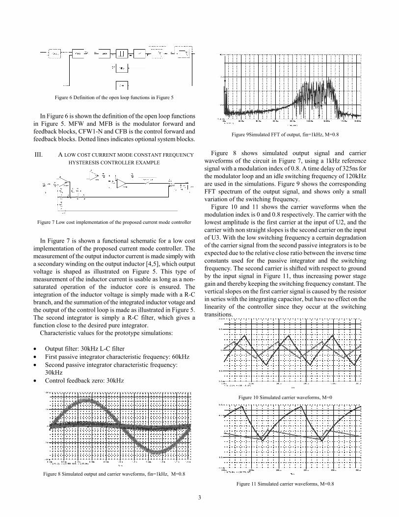
Figure 6 Definition of the open loop functions in Figure 5
In Figure 6 is shown the definition of the open loop functions
in Figure 5 MFW and MFB is the modulator forward and feedback blocks CFW1-N and CFB is the control forward and feedback blocks Dotted lines indicates optional system blocks
III A LOW COST CURRENT MODE CONSTANT FREQUENCY HYSTERESIS CONTROLLER EXAMPLE
Figure 7 Low cost implementation of the proposed current mode controller
In Figure 7 is shown a functional schematic for a low cost
implementation of the proposed current mode controller The measurement of the output inductor current is made simply with a secondary winding on the output inductor [45] which output voltage is shaped as illustrated on Figure 5 This type of measurement of the inductor current is usable as long as a non-saturated operation of the inductor core is ensured The integration of the inductor voltage is simply made with a R-C branch and the summation of the integrated inductor votage and the output of the control loop is made as illustrated in Figure 5 The second integrator is simply a R-C filter which gives a function close to the desired pure integrator
Characteristic values for the prototype simulations
bull Output filter 30kHz L-C filter bull First passive integrator characteristic frequency 60kHz bull Second passive integrator characteristic frequency
30kHz bull Control feedback zero 30kHz
Figure 8 Simulated output and carrier waveforms fin=1kHz M=08
Figure 9Simulated FFT of output fin=1kHz M=08
Figure 8 shows simulated output signal and carrier
waveforms of the circuit in Figure 7 using a 1kHz reference signal with a modulation index of 08 A time delay of 325ns for the modulator loop and an idle switching frequency of 120kHz are used in the simulations Figure 9 shows the corresponding FFT spectrum of the output signal and shows only a small variation of the switching frequency
Figure 10 and 11 shows the carrier waveforms when the modulation index is 0 and 08 respectively The carrier with the lowest amplitude is the first carrier at the input of U2 and the carrier with non straight slopes is the second carrier on the input of U3 With the low switching frequency a certain degradation of the carrier signal from the second passive integrators is to be expected due to the relative close ratio between the inverse time constants used for the passive integrator and the switching frequency The second carrier is shifted with respect to ground by the input signal in Figure 11 thus increasing power stage gain and thereby keeping the switching frequency constant The vertical slopes on the first carrier signal is caused by the resistor in series with the integrating capacitor but have no effect on the linearity of the controller since they occur at the switching transitions
Figure 10 Simulated carrier waveforms M=0
Figure 11 Simulated carrier waveforms M=08
4
IV 3-LEVEL VOLTAGE MODE FIXED FREQUENCY HYSTERESIS CONTROLLER EXAMPLE
Figure 12 Proposed synchronized 3-level voltage mode controller
Figure 12 illustrates one implementation of two voltage mode
controllers of the proposed topology synchronized for a 3-level modulated output The implementation shown is a low cost implementation comparable to the current mode example above The same synchronization can be made with the proposed current mode controller and the voltage mode modulator in Figure 12 can be realized as a single modulator without any synchronization as well The synchronization is obtained by coupling the two hysteresis blocks with an impedance in this model a simple resistor This impedance synchronizes the two second carriers in a way that makes the two triangular shaped carriers in phase at high frequencies Compared to synchronization of basic of hysteresis controllers or other types of self oscillating oscillators [6] the two carriers will cause less distortion on each other caused by the pure triangular shape
Figure 13 Simulated output amp carrier waveforms fin=1kHz M=08
Figure 14 Simulated carrier Waveforms M=08
Figure 13 and Figure 14 show waveforms from the circuit in
Figure 12 a time delay of 325 ns is used in the power stage model and an idle switching frequency of 150kHz The pulse signal is the differential output of the two power stages shown in Figure 12 In Figure 14 is shown the carrier waveforms when the output is at its maximum where the sawtooth shaped carriers are the first carriers at the input of U2 and the triangular are the second carriers on the input of U3
V EXPERIMENTAL RESULTS
Figure 15 Constant switching frequency prototype
A prototype of the proposed constant frequency hysteresis
modulator illustrated in Figure 7 has been build The prototype is realized as a low cost solution with the modulator loop based on LM319 comparators The achieved total time delay trough the modulator loop is in the order of 325ns due to the 80ns propagation delay of each comparator as well as the delay from the HIP2106 FET driver and two logic devices The prototype was running with an idle switching frequency of 120kHz which is low for full bandwidth audio applications but sufficient to prove the theory of operation Nevertheless the prototype was able to prove the constant switching frequency behavior
Prototype measurements
0
02
04
06
08
1
12
0 01 02 03 04 05 06 07 08 09
Modulation index [M]
fs(M
) rel
to fs
0
Prototype Std Hyst
Figure 16 Prototype and standard hysteresis controller normalized switching frequency vs M
5
Figure 16 shows measured switching frequency vs
modulation index M for DC operation normalized with the idle switching frequency The results are shown together with values expected with a standard hysteresis modulator It is clearly seen that the degradation of the switching frequency is significant smaller with the proposed modulator than with a standard hysteresis modulator
Figure 17 Prototype carrier waveforms M=0
Figure 18 Prototype carrier waveforms M=08
Figure 17 and 18 shows carrier waveforms for the prototype
for M=0 and M=08 The waveforms corresponds to the simulated waveforms in Figure 10 and 11 The shape of the first carrier signal is purely sawtooth shaped due to the combination of the inner modulator loop and the outer control loop where the high frequency components are controlled to add up to a perfect carrier waveform with straight slopes
Figure 19 Prototype FFT fin=10Hz M=08
Figure 20 Prototype FFT fin=100Hz M=08
Figure 21 Prototype FFT fin=1kHz M=08
Figure 19-21 shows FFT of the switching frequency for the
prototype A sinusoidal input signal of 10Hz 100Hz and 1kHz is used with a maximum modulation index of 08 The constant frequency behavior is best obtained with low input frequencies as expected but even with 1kHz the minimum switching frequency is 67 of the idle switching frequency compared to an expected 36 for a standard hysteresis modulator
6
VI CONCLUSION A constant switching frequency hysteresis controller is
proposed The controller can be of either current or voltage mode operation The proposed controller differs from prior art hysteresis controllers by having a second integrator inserted in the controller loops forward path thus increasing power stage gain with increasing input signal level The fixed frequency controller maintains the controller loops bandwidth and gain at all modulation indexes thus maintaining high performance at all signal levels Furthermore a low cost implementation of the proposed controller with an additional control loop is illustrated in a way that maintains the perfect sawtooth carrier waveform ensuring high linearity The constant switching frequency behavior of the modulator maintains modulator loop open loop gain and -bandwidth for all modulation indexes which means that performance is not degraded at high modulation indexes as is the case with standard hysteresis controllers
The proposed controller can be made as either a single 2-level or a synchronized 3-level modulator
The constant switching frequency behavior of the modulator is proved by simulations and prototype measurements
ACKNOWLEDGMENTS The work presented in this paper is some of the results from
an on-going PhD research project ACT - ACtive Transducers at Technical University of Denmark financed by The Danish Energy Authority journal number 127301-006 The project is in co-operation with Bang amp Olufsen ICEpower AS and Danish Sound Technology AS
REFERENCES [1] Robert W Erickson Dragan Maksimovic Fundamentals of Power
Electronics Second Edition 2001 ISBN 0-7923-7270-0 page 657-659 [2] ELBO GmbH Selbstshwingender Digitalverstaumlrker DE 198 38 765 A1
German patent May 2000 [3] Andreacute Veltman Johannes Jacobus Hendrikus Amplifier Circuit WO
0042702 Int patent January 2000 [4] Allen F Rozman Jeffrey J Boylan Band Pass Current Control IEEE
May 1994 [5] F C Lee R P Iwens Y Yu Generalized Computer-aided Discrete Time
Domain Modelling And Analysis Of DC-DC Converters PESC 77 Record [6] Karsten Nielsen Jesper Lind Hansen Synchronized Controlled Oscillation
Modulator WO 03055060 A1 Int patent July 2003

2
( ) ( )20 1s sf M f M= sdot minus
The variation in switching frequency basically causes two
main functional problems Increased high frequency ripple voltage on the output at high modulation index caused by less attenuation of the lower switching frequencys harmonics and reduced open loop bandwidth and -loop gain causing increased distortion as well A variable hysteresis window that follows M or the absolute value of the input signal has been proposed in prior art [3] If the variable hysteresis window is made such that it follows the square of the absolute value as well as the derivative of the input signal the switching frequency can be made constant but at a much higher system complexity than the basic design In this paper a second integrator block inserted before the hysteresis window in either a current or a voltage mode controller is proposed to obtain a close to constant switching frequency regardless of M
Figure 3 Proposed current mode controller
Figure 4 Proposed voltage mode controller
The proposed modulator is shown in Figure 3 and Figure 4
for both current and voltage mode operation The extra integrator integrates the sign of the first sawtooth shaped carrier signal which results in a pure triangular shaped second carrier overlapped by the reference signal The PWM signal to the power stage is made from the second carrier signal fed into a hysteresis window The modulator loop has maintained a 1st order behavior at high frequencies since the first comparator effectively differentiates the high frequencies and followed by the second integrator the -90ordm phase shift at high frequencies is maintained
The variable modulator forward gain is made by the second carrier signal which will be a triangular shaped signal overlapped by the reference signal For a DC reference signal the second integrator will simply increase the forward gain by shift the second carrier signal with respect to ground and ideally obtaining exactly the same forward gain and thereby the same switching frequency at all modulation indexes M The ability of keeping the switching frequency constant depends on the slopes of the reference signal since the correction of the falling switching frequency corresponds to the gain of the second integrator which means that the switching frequency will have larger deviations from a constant value with high frequency reference signals at high levels but if the time
constant of the second integrator is high compared to the corresponding time constant for the reference signal only small variations will occur at the switching frequency Because of the constant switching frequency the open loop gain and -bandwidth is maintained and performance of the controller is not reduced at high M
II REQUIREMENT FOR SWITCH MODE AUDIO AMPLIFIERPRECISION CONTROLLERS
The main performance requirement for audio amplifiers is low distortion Even though the basic hysteresis controller has excellent linearity in the idealized implementation additional control loops are often required to obtain the specified performance The largest source of distortion is the power stage and it is often required to have a larger reduction of this distortion than the abilities of the modulator itself Another key parameter is high frequency noise on the output When using a modulator with a switching frequency decreasing with increasing M a high switching frequency is often required to ensure low high frequency noise on the output Furthermore the strongly varying switching frequency makes design of additional control loops difficult because of the changing loop bandwidth and -gain for the modulator loop itself
When applying additional control loops the cleanliness of the carrier is of severe importance It is impossible to design a stable control loop totally without any high frequency components from the switching frequency and its harmonics When the output of the control loop holds a high frequency output this high frequency content will effectively add to the sawtooth shaped carrier and thereby distort the carrier and thus compromising performance However if the inner control loop is designed together with the additional control loop in such a way that the high frequency content on the output of the control loop is missing in the generation of the carrier in the inner controller loop the high frequency components will summarize to the ideal sawtooth shaped carrier waveform
Figure 5 Combining inner and outer loop functions
Figure 5 illustrates how the inner controller loop and the outer control loop can be shaped to achieve the desired pure 1 order function for the combined circuit This will be met if the phase of the control loop is shifted 180ordm with respect to the phase of the controller loop at high frequencies ensuring generation of a perfect sawtooth shaped carrier signal
3
Figure 6 Definition of the open loop functions in Figure 5
In Figure 6 is shown the definition of the open loop functions
in Figure 5 MFW and MFB is the modulator forward and feedback blocks CFW1-N and CFB is the control forward and feedback blocks Dotted lines indicates optional system blocks
III A LOW COST CURRENT MODE CONSTANT FREQUENCY HYSTERESIS CONTROLLER EXAMPLE
Figure 7 Low cost implementation of the proposed current mode controller
In Figure 7 is shown a functional schematic for a low cost
implementation of the proposed current mode controller The measurement of the output inductor current is made simply with a secondary winding on the output inductor [45] which output voltage is shaped as illustrated on Figure 5 This type of measurement of the inductor current is usable as long as a non-saturated operation of the inductor core is ensured The integration of the inductor voltage is simply made with a R-C branch and the summation of the integrated inductor votage and the output of the control loop is made as illustrated in Figure 5 The second integrator is simply a R-C filter which gives a function close to the desired pure integrator
Characteristic values for the prototype simulations
bull Output filter 30kHz L-C filter bull First passive integrator characteristic frequency 60kHz bull Second passive integrator characteristic frequency
30kHz bull Control feedback zero 30kHz
Figure 8 Simulated output and carrier waveforms fin=1kHz M=08
Figure 9Simulated FFT of output fin=1kHz M=08
Figure 8 shows simulated output signal and carrier
waveforms of the circuit in Figure 7 using a 1kHz reference signal with a modulation index of 08 A time delay of 325ns for the modulator loop and an idle switching frequency of 120kHz are used in the simulations Figure 9 shows the corresponding FFT spectrum of the output signal and shows only a small variation of the switching frequency
Figure 10 and 11 shows the carrier waveforms when the modulation index is 0 and 08 respectively The carrier with the lowest amplitude is the first carrier at the input of U2 and the carrier with non straight slopes is the second carrier on the input of U3 With the low switching frequency a certain degradation of the carrier signal from the second passive integrators is to be expected due to the relative close ratio between the inverse time constants used for the passive integrator and the switching frequency The second carrier is shifted with respect to ground by the input signal in Figure 11 thus increasing power stage gain and thereby keeping the switching frequency constant The vertical slopes on the first carrier signal is caused by the resistor in series with the integrating capacitor but have no effect on the linearity of the controller since they occur at the switching transitions
Figure 10 Simulated carrier waveforms M=0
Figure 11 Simulated carrier waveforms M=08
4
IV 3-LEVEL VOLTAGE MODE FIXED FREQUENCY HYSTERESIS CONTROLLER EXAMPLE
Figure 12 Proposed synchronized 3-level voltage mode controller
Figure 12 illustrates one implementation of two voltage mode
controllers of the proposed topology synchronized for a 3-level modulated output The implementation shown is a low cost implementation comparable to the current mode example above The same synchronization can be made with the proposed current mode controller and the voltage mode modulator in Figure 12 can be realized as a single modulator without any synchronization as well The synchronization is obtained by coupling the two hysteresis blocks with an impedance in this model a simple resistor This impedance synchronizes the two second carriers in a way that makes the two triangular shaped carriers in phase at high frequencies Compared to synchronization of basic of hysteresis controllers or other types of self oscillating oscillators [6] the two carriers will cause less distortion on each other caused by the pure triangular shape
Figure 13 Simulated output amp carrier waveforms fin=1kHz M=08
Figure 14 Simulated carrier Waveforms M=08
Figure 13 and Figure 14 show waveforms from the circuit in
Figure 12 a time delay of 325 ns is used in the power stage model and an idle switching frequency of 150kHz The pulse signal is the differential output of the two power stages shown in Figure 12 In Figure 14 is shown the carrier waveforms when the output is at its maximum where the sawtooth shaped carriers are the first carriers at the input of U2 and the triangular are the second carriers on the input of U3
V EXPERIMENTAL RESULTS
Figure 15 Constant switching frequency prototype
A prototype of the proposed constant frequency hysteresis
modulator illustrated in Figure 7 has been build The prototype is realized as a low cost solution with the modulator loop based on LM319 comparators The achieved total time delay trough the modulator loop is in the order of 325ns due to the 80ns propagation delay of each comparator as well as the delay from the HIP2106 FET driver and two logic devices The prototype was running with an idle switching frequency of 120kHz which is low for full bandwidth audio applications but sufficient to prove the theory of operation Nevertheless the prototype was able to prove the constant switching frequency behavior
Prototype measurements
0
02
04
06
08
1
12
0 01 02 03 04 05 06 07 08 09
Modulation index [M]
fs(M
) rel
to fs
0
Prototype Std Hyst
Figure 16 Prototype and standard hysteresis controller normalized switching frequency vs M
5
Figure 16 shows measured switching frequency vs
modulation index M for DC operation normalized with the idle switching frequency The results are shown together with values expected with a standard hysteresis modulator It is clearly seen that the degradation of the switching frequency is significant smaller with the proposed modulator than with a standard hysteresis modulator
Figure 17 Prototype carrier waveforms M=0
Figure 18 Prototype carrier waveforms M=08
Figure 17 and 18 shows carrier waveforms for the prototype
for M=0 and M=08 The waveforms corresponds to the simulated waveforms in Figure 10 and 11 The shape of the first carrier signal is purely sawtooth shaped due to the combination of the inner modulator loop and the outer control loop where the high frequency components are controlled to add up to a perfect carrier waveform with straight slopes
Figure 19 Prototype FFT fin=10Hz M=08
Figure 20 Prototype FFT fin=100Hz M=08
Figure 21 Prototype FFT fin=1kHz M=08
Figure 19-21 shows FFT of the switching frequency for the
prototype A sinusoidal input signal of 10Hz 100Hz and 1kHz is used with a maximum modulation index of 08 The constant frequency behavior is best obtained with low input frequencies as expected but even with 1kHz the minimum switching frequency is 67 of the idle switching frequency compared to an expected 36 for a standard hysteresis modulator
6
VI CONCLUSION A constant switching frequency hysteresis controller is
proposed The controller can be of either current or voltage mode operation The proposed controller differs from prior art hysteresis controllers by having a second integrator inserted in the controller loops forward path thus increasing power stage gain with increasing input signal level The fixed frequency controller maintains the controller loops bandwidth and gain at all modulation indexes thus maintaining high performance at all signal levels Furthermore a low cost implementation of the proposed controller with an additional control loop is illustrated in a way that maintains the perfect sawtooth carrier waveform ensuring high linearity The constant switching frequency behavior of the modulator maintains modulator loop open loop gain and -bandwidth for all modulation indexes which means that performance is not degraded at high modulation indexes as is the case with standard hysteresis controllers
The proposed controller can be made as either a single 2-level or a synchronized 3-level modulator
The constant switching frequency behavior of the modulator is proved by simulations and prototype measurements
ACKNOWLEDGMENTS The work presented in this paper is some of the results from
an on-going PhD research project ACT - ACtive Transducers at Technical University of Denmark financed by The Danish Energy Authority journal number 127301-006 The project is in co-operation with Bang amp Olufsen ICEpower AS and Danish Sound Technology AS
REFERENCES [1] Robert W Erickson Dragan Maksimovic Fundamentals of Power
Electronics Second Edition 2001 ISBN 0-7923-7270-0 page 657-659 [2] ELBO GmbH Selbstshwingender Digitalverstaumlrker DE 198 38 765 A1
German patent May 2000 [3] Andreacute Veltman Johannes Jacobus Hendrikus Amplifier Circuit WO
0042702 Int patent January 2000 [4] Allen F Rozman Jeffrey J Boylan Band Pass Current Control IEEE
May 1994 [5] F C Lee R P Iwens Y Yu Generalized Computer-aided Discrete Time
Domain Modelling And Analysis Of DC-DC Converters PESC 77 Record [6] Karsten Nielsen Jesper Lind Hansen Synchronized Controlled Oscillation
Modulator WO 03055060 A1 Int patent July 2003