effect of valley switching and switching-frequency ... ccm huber.pdfeffect of valley switching and...
TRANSCRIPT
IEEE TRANSACTIONS ON POWER ELECTRONICS, VOL. 24, NO. 2, FEBRUARY 2009 339
Effect of Valley Switching and Switching-FrequencyLimitation on Line-Current Distortions of
DCM/CCM Boundary Boost PFC ConvertersLaszlo Huber, Member, IEEE, Brian T. Irving, and Milan M. Jovanovic, Fellow, IEEE
Abstract—A systematic analysis of line-current distortions of thediscontinuous-conduction-mode and the continuous-conduction-mode boundary boost power factor correction converter due to val-ley switching (VS) and switching-frequency limitation, where VSis either maintained or lost after the onset of switching-frequencylimitation, is provided. Closed-form expressions for the line currentare derived. It is shown that if the switching frequency is limitedand VS is not maintained, the line current is more distorted withvoltage-mode control than with current-mode control. The effectsof line-current distortions are demonstrated with both simulationand experimental results.
Index Terms—Boost converter, discontinuous conduction mode(DCM)/continuous conduction mode (CCM) boundary, line-current distortion, power factor correction (PFC), single-phaserectifier, switching-frequency limitation, valley switching (VS).
I. INTRODUCTION
IN LOW-POWER offline power supplies, a boost converter(see Fig. 1) operating at the boundary of the discontinu-
ous conduction mode (DCM) and continuous conduction mode(CCM) is a popular topology for implementing the front-endconverter with active power factor correction (PFC) [1]–[9].The major benefit of the DCM/CCM boundary boost converter,compared to the CCM boost converter, is that the reverse re-covery losses related to the boost diode are eliminated [12].In addition, turn-on with zero-voltage switching (ZVS) or nearZVS of the boost switch, also called valley switching (VS),can be easily achieved [9]–[11]. VS is due to the resonance be-tween the parasitic capacitances of the boost switch and boostdiode with the boost inductor after the demagnetization of theboost inductor. Neither the CCM nor the DCM boost PFC con-verter, which operate with a constant switching frequency, canachieve ZVS without an additional active snubber circuit [12].Other benefits of the DCM/CCM boundary boost PFC convertercompared to the constant-switching-frequency DCM boost PFCconverter [13], [14] are a lower total harmonic distortion (THD)of the line current and a smaller peak inductor current result-
Manuscript received April 3, 2008; revised July 11, 2008. First publishedDecember 22, 2008; current version published February 6, 2009. This paperwas presented at the 23rd Annual IEEE Applied Power Electronics Conference(APEC), Austin, TX, February 24–28, 2008. Recommended for publication byAssociate Editor D. Perreault.
The authors are with Delta Products Corporation, Power ElectronicsLaboratory, Research Triangle Park, NC 27709 USA (e-mail: [email protected]).
Color versions of one or more of the figures in this paper are available onlineat http://ieeexplore.ieee.org.
Digital Object Identifier 10.1109/TPEL.2008.2006053
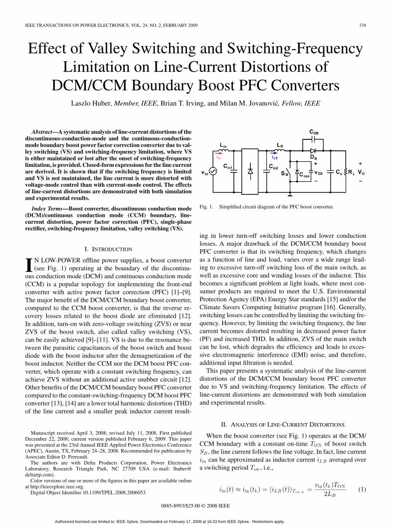
Fig. 1. Simplified circuit diagram of the PFC boost converter.
ing in lower turn-off switching losses and lower conductionlosses. A major drawback of the DCM/CCM boundary boostPFC converter is that its switching frequency, which changesas a function of line and load, varies over a wide range lead-ing to excessive turn-off switching loss of the main switch, aswell as excessive core and winding losses of the inductor. Thisbecomes a significant problem at light loads, where most con-sumer products are required to meet the U.S. EnvironmentalProtection Agency (EPA) Energy Star standards [15] and/or theClimate Savers Computing Initiative program [16]. Generally,switching losses can be controlled by limiting the switching fre-quency. However, by limiting the switching frequency, the linecurrent becomes distorted resulting in decreased power factor(PF) and increased THD. In addition, ZVS of the main switchcan be lost, which degrades the efficiency and leads to exces-sive electromagnetic interference (EMI) noise, and therefore,additional input filtration is needed.
This paper presents a systematic analysis of the line-currentdistortions of the DCM/CCM boundary boost PFC converterdue to VS and switching-frequency limitation. The effects ofline-current distortions are demonstrated with both simulationand experimental results.
II. ANALYSIS OF LINE-CURRENT DISTORTIONS
When the boost converter (see Fig. 1) operates at the DCM/CCM boundary with a constant on-time TON of boost switchSB , the line current follows the line voltage. In fact, line currentiin can be approximated as inductor current iLB averaged overa switching period Tsw , i.e.,
iin(t) ≈ iin (tk ) = 〈iLB (t)〉T sw , k=
vin(tk )TON
2LB(1)
0885-8993/$25.00 © 2008 IEEE
Authorized licensed use limited to: IEEE Xplore. Downloaded on February 17, 2009 at 16:33 from IEEE Xplore. Restrictions apply.
340 IEEE TRANSACTIONS ON POWER ELECTRONICS, VOL. 24, NO. 2, FEBRUARY 2009
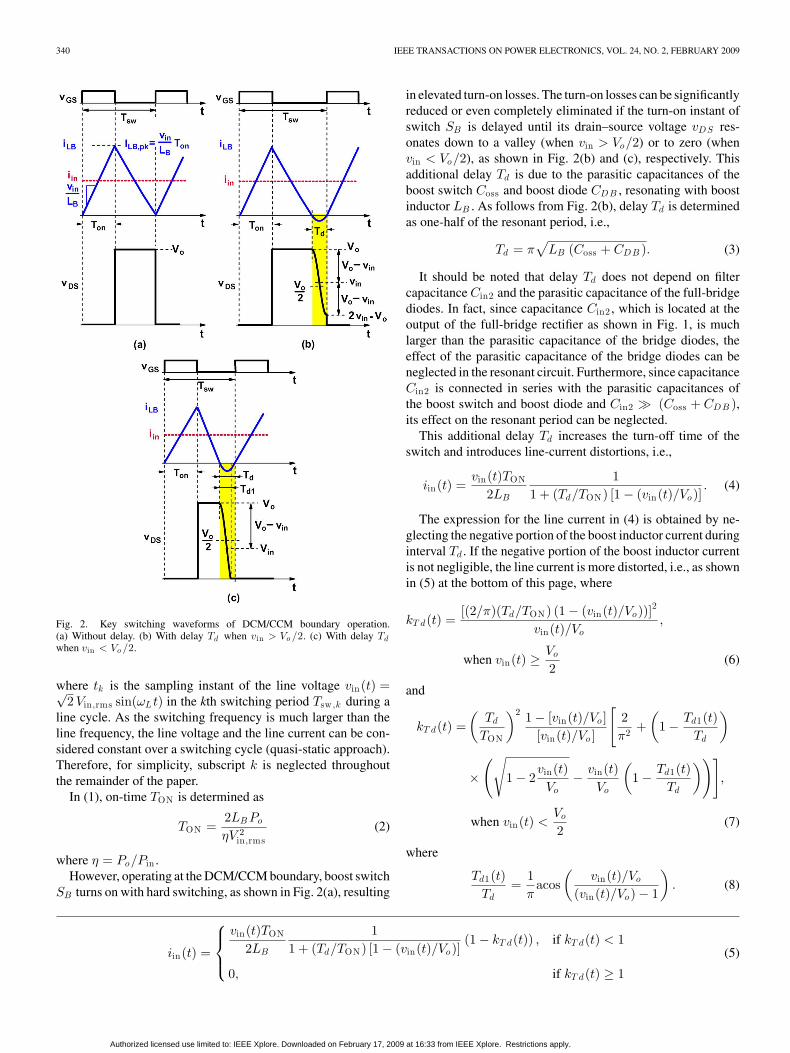
Fig. 2. Key switching waveforms of DCM/CCM boundary operation.(a) Without delay. (b) With delay Td when vin > Vo /2. (c) With delay Td
when vin < Vo /2.
where tk is the sampling instant of the line voltage vin(t) =√2 Vin,rms sin(ωLt) in the kth switching period Tsw ,k during a
line cycle. As the switching frequency is much larger than theline frequency, the line voltage and the line current can be con-sidered constant over a switching cycle (quasi-static approach).Therefore, for simplicity, subscript k is neglected throughoutthe remainder of the paper.
In (1), on-time TON is determined as
TON =2LB Po
ηV 2in,rms
(2)
where η = Po/Pin .However, operating at the DCM/CCM boundary, boost switch
SB turns on with hard switching, as shown in Fig. 2(a), resulting
in elevated turn-on losses. The turn-on losses can be significantlyreduced or even completely eliminated if the turn-on instant ofswitch SB is delayed until its drain–source voltage vDS res-onates down to a valley (when vin > Vo/2) or to zero (whenvin < Vo/2), as shown in Fig. 2(b) and (c), respectively. Thisadditional delay Td is due to the parasitic capacitances of theboost switch Coss and boost diode CDB , resonating with boostinductor LB . As follows from Fig. 2(b), delay Td is determinedas one-half of the resonant period, i.e.,
Td = π√
LB (Coss + CDB ). (3)
It should be noted that delay Td does not depend on filtercapacitance Cin2 and the parasitic capacitance of the full-bridgediodes. In fact, since capacitance Cin2 , which is located at theoutput of the full-bridge rectifier as shown in Fig. 1, is muchlarger than the parasitic capacitance of the bridge diodes, theeffect of the parasitic capacitance of the bridge diodes can beneglected in the resonant circuit. Furthermore, since capacitanceCin2 is connected in series with the parasitic capacitances ofthe boost switch and boost diode and Cin2 � (Coss + CDB ),its effect on the resonant period can be neglected.
This additional delay Td increases the turn-off time of theswitch and introduces line-current distortions, i.e.,
iin(t) =vin(t)TON
2LB
11 + (Td/TON) [1 − (vin(t)/Vo)]
. (4)
The expression for the line current in (4) is obtained by ne-glecting the negative portion of the boost inductor current duringinterval Td . If the negative portion of the boost inductor currentis not negligible, the line current is more distorted, i.e., as shownin (5) at the bottom of this page, where
kT d(t) =[(2/π)(Td/TON) (1 − (vin(t)/Vo))]
2
vin(t)/Vo,
when vin(t) ≥ Vo
2(6)
and
kT d(t) =(
Td
TON
)2 1 − [vin(t)/Vo ][vin(t)/Vo ]
[2π2 +
(1 − Td1(t)
Td
)
×(√
1 − 2vin(t)Vo
− vin(t)Vo
(1 − Td1(t)
Td
))],
when vin(t) <Vo
2(7)
where
Td1(t)Td
=1π
acos(
vin(t)/Vo
(vin(t)/Vo) − 1
). (8)
iin(t) =
vin(t)TON
2LB
11 + (Td/TON) [1 − (vin(t)/Vo)]
(1 − kT d(t)) , if kT d(t) < 1
0, if kT d(t) ≥ 1
(5)
Authorized licensed use limited to: IEEE Xplore. Downloaded on February 17, 2009 at 16:33 from IEEE Xplore. Restrictions apply.
HUBER et al.: EFFECT OF VALLEY SWITCHING AND SWITCHING-FREQUENCY LIMITATION ON LINE-CURRENT DISTORTIONS 341
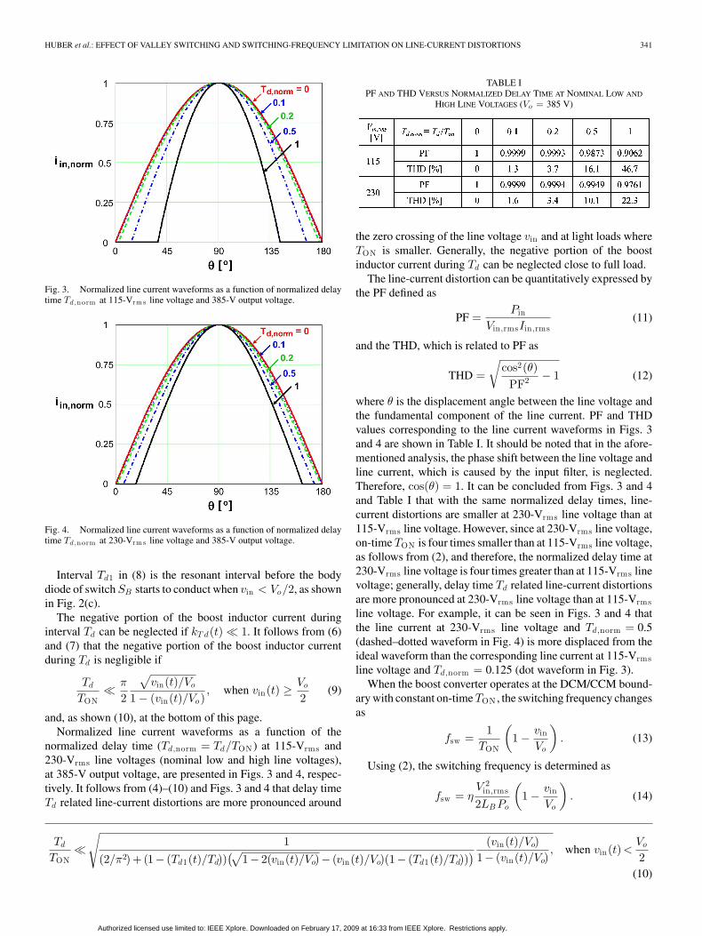
Fig. 3. Normalized line current waveforms as a function of normalized delaytime Td,norm at 115-Vrm s line voltage and 385-V output voltage.
Fig. 4. Normalized line current waveforms as a function of normalized delaytime Td,norm at 230-Vrm s line voltage and 385-V output voltage.
Interval Td1 in (8) is the resonant interval before the bodydiode of switch SB starts to conduct when vin < Vo/2, as shownin Fig. 2(c).
The negative portion of the boost inductor current duringinterval Td can be neglected if kT d(t) � 1. It follows from (6)and (7) that the negative portion of the boost inductor currentduring Td is negligible if
Td
TON� π
2
√vin(t)/Vo
1 − (vin(t)/Vo), when vin(t) ≥ Vo
2(9)
and, as shown (10), at the bottom of this page.Normalized line current waveforms as a function of the
normalized delay time (Td,norm = Td/TON ) at 115-Vrms and230-Vrms line voltages (nominal low and high line voltages),at 385-V output voltage, are presented in Figs. 3 and 4, respec-tively. It follows from (4)–(10) and Figs. 3 and 4 that delay timeTd related line-current distortions are more pronounced around
TABLE IPF AND THD VERSUS NORMALIZED DELAY TIME AT NOMINAL LOW AND
HIGH LINE VOLTAGES (Vo = 385 V)
the zero crossing of the line voltage vin and at light loads whereTON is smaller. Generally, the negative portion of the boostinductor current during Td can be neglected close to full load.
The line-current distortion can be quantitatively expressed bythe PF defined as
PF =Pin
Vin,rmsIin,rms(11)
and the THD, which is related to PF as
THD =
√cos2(θ)PF2 − 1 (12)
where θ is the displacement angle between the line voltage andthe fundamental component of the line current. PF and THDvalues corresponding to the line current waveforms in Figs. 3and 4 are shown in Table I. It should be noted that in the afore-mentioned analysis, the phase shift between the line voltage andline current, which is caused by the input filter, is neglected.Therefore, cos(θ) = 1. It can be concluded from Figs. 3 and 4and Table I that with the same normalized delay times, line-current distortions are smaller at 230-Vrms line voltage than at115-Vrms line voltage. However, since at 230-Vrms line voltage,on-time TON is four times smaller than at 115-Vrms line voltage,as follows from (2), and therefore, the normalized delay time at230-Vrms line voltage is four times greater than at 115-Vrms linevoltage; generally, delay time Td related line-current distortionsare more pronounced at 230-Vrms line voltage than at 115-Vrmsline voltage. For example, it can be seen in Figs. 3 and 4 thatthe line current at 230-Vrms line voltage and Td,norm = 0.5(dashed–dotted waveform in Fig. 4) is more displaced from theideal waveform than the corresponding line current at 115-Vrmsline voltage and Td,norm = 0.125 (dot waveform in Fig. 3).
When the boost converter operates at the DCM/CCM bound-ary with constant on-time TON , the switching frequency changesas
fsw =1
TON
(1 − vin
Vo
). (13)
Using (2), the switching frequency is determined as
fsw = ηV 2
in,rms
2LB Po
(1 − vin
Vo
). (14)
Td
TON�
√1
(2/π2) + (1− (Td1(t)/Td))(√
1− 2(vin(t)/Vo)− (vin(t)/Vo)(1− (Td1(t)/Td))) (vin(t)/Vo)
1− (vin(t)/Vo), when vin(t)<
Vo
2(10)
Authorized licensed use limited to: IEEE Xplore. Downloaded on February 17, 2009 at 16:33 from IEEE Xplore. Restrictions apply.
342 IEEE TRANSACTIONS ON POWER ELECTRONICS, VOL. 24, NO. 2, FEBRUARY 2009
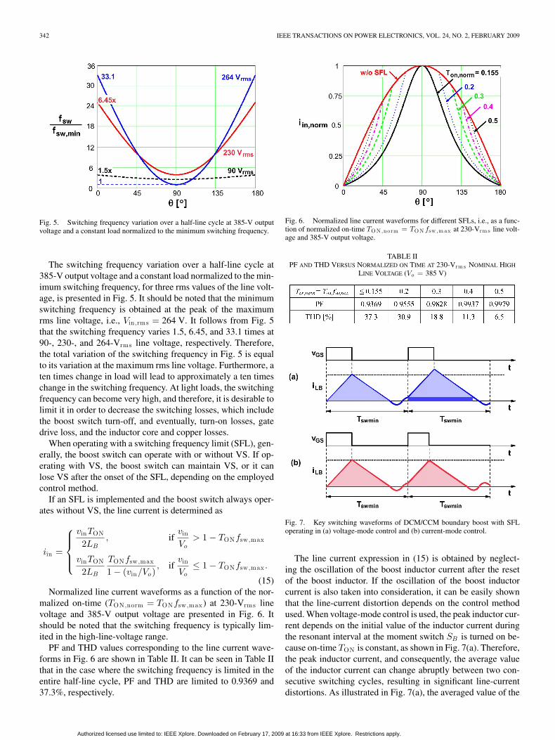
Fig. 5. Switching frequency variation over a half-line cycle at 385-V outputvoltage and a constant load normalized to the minimum switching frequency.
The switching frequency variation over a half-line cycle at385-V output voltage and a constant load normalized to the min-imum switching frequency, for three rms values of the line volt-age, is presented in Fig. 5. It should be noted that the minimumswitching frequency is obtained at the peak of the maximumrms line voltage, i.e., Vin,rms = 264 V. It follows from Fig. 5that the switching frequency varies 1.5, 6.45, and 33.1 times at90-, 230-, and 264-Vrms line voltage, respectively. Therefore,the total variation of the switching frequency in Fig. 5 is equalto its variation at the maximum rms line voltage. Furthermore, aten times change in load will lead to approximately a ten timeschange in the switching frequency. At light loads, the switchingfrequency can become very high, and therefore, it is desirable tolimit it in order to decrease the switching losses, which includethe boost switch turn-off, and eventually, turn-on losses, gatedrive loss, and the inductor core and copper losses.
When operating with a switching frequency limit (SFL), gen-erally, the boost switch can operate with or without VS. If op-erating with VS, the boost switch can maintain VS, or it canlose VS after the onset of the SFL, depending on the employedcontrol method.
If an SFL is implemented and the boost switch always oper-ates without VS, the line current is determined as
iin =
vinTON
2LB, if
vin
Vo> 1 − TONfsw ,max
vinTON
2LB
TONfsw ,max
1 − (vin/Vo), if
vin
Vo≤ 1 − TONfsw ,max .
(15)Normalized line current waveforms as a function of the nor-
malized on-time (TON ,norm = TONfsw ,max ) at 230-Vrms linevoltage and 385-V output voltage are presented in Fig. 6. Itshould be noted that the switching frequency is typically lim-ited in the high-line-voltage range.
PF and THD values corresponding to the line current wave-forms in Fig. 6 are shown in Table II. It can be seen in Table IIthat in the case where the switching frequency is limited in theentire half-line cycle, PF and THD are limited to 0.9369 and37.3%, respectively.
Fig. 6. Normalized line current waveforms for different SFLs, i.e., as a func-tion of normalized on-time TON ,norm = TON fsw ,m ax at 230-Vrm s line volt-age and 385-V output voltage.
TABLE IIPF AND THD VERSUS NORMALIZED ON TIME AT 230-Vrm s NOMINAL HIGH
LINE VOLTAGE (Vo = 385 V)
Fig. 7. Key switching waveforms of DCM/CCM boundary boost with SFLoperating in (a) voltage-mode control and (b) current-mode control.
The line current expression in (15) is obtained by neglect-ing the oscillation of the boost inductor current after the resetof the boost inductor. If the oscillation of the boost inductorcurrent is also taken into consideration, it can be easily shownthat the line-current distortion depends on the control methodused. When voltage-mode control is used, the peak inductor cur-rent depends on the initial value of the inductor current duringthe resonant interval at the moment switch SB is turned on be-cause on-time TON is constant, as shown in Fig. 7(a). Therefore,the peak inductor current, and consequently, the average valueof the inductor current can change abruptly between two con-secutive switching cycles, resulting in significant line-currentdistortions. As illustrated in Fig. 7(a), the averaged value of the
Authorized licensed use limited to: IEEE Xplore. Downloaded on February 17, 2009 at 16:33 from IEEE Xplore. Restrictions apply.
HUBER et al.: EFFECT OF VALLEY SWITCHING AND SWITCHING-FREQUENCY LIMITATION ON LINE-CURRENT DISTORTIONS 343
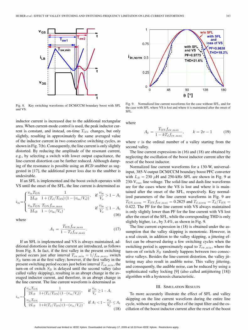
Fig. 8. Key switching waveforms of DCM/CCM boundary boost with SFLand VS.
inductor current is increased due to the additional rectangulararea. When current-mode control is used, the peak inductor cur-rent is constant, and instead, on-time TON changes, but onlyslightly, resulting in approximately the same averaged valueof the inductor current in two consecutive switching cycles, asshown in Fig. 7(b). Consequently, the line current is only slightlydistorted. By reducing the amplitude of the resonant current,e.g., by selecting a switch with lower output capacitance, theline-current distortion can be further reduced. Although damp-ing of the resonance is possible using an RCD snubber as sug-gested in [17], the additional power loss due to the snubber isundesirable.
If an SFL is implemented and the boost switch operates withVS until the onset of the SFL, the line current is determined as
iin=
vinTON
2LB
11 + (Td/TON) (1− (vin/Vo))
, ifvin
Vo> 1−A1
vinTON
2LB
TONfsw ,max
1 − (vin/Vo), if
vin
Vo≤ 1−A1
(16)where
A1 =TONfsw ,max
1 − Tdfsw ,max. (17)
If an SFL is implemented and VS is always maintained, ad-ditional distortions in the line current are introduced, as followsfrom Fig. 8. In fact, if the first valley in the present switchingperiod occurs just after interval Tsw ,min = 1/fsw ,max , switchSB turns on at the first valley; however, if the first valley in thepresent switching period occurs just before interval Tsw ,min , theturn-on of switch SB is delayed until the second valley (alsocalled valley skipping), resulting in an abrupt change in the av-eraged inductor current, and therefore, in an abrupt change inthe line current. The line current waveform is determined as
iin=
vinTON
2LB
11+(Td/TON) (1−(vin/Vo))
, ifvin
Vo≥ 1−A1
vinTON
2LB
11+k(Td/TON) (1−(vin/Vo))
, if A1 < 1− vin
Vo≤Ak
(18)
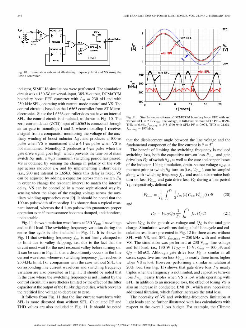
Fig. 9. Normalized line current waveforms for the case without SFL, and forthe case with SFL where VS is lost and where it is maintained after the onset ofSFL.
where
Ak =TONfsw ,max
1 − kTdfsw ,max, k = 2v − 1 (19)
where v is the ordinal number of a valley starting from thesecond valley.
The line current expressions in (16) and (18) are obtained byneglecting the oscillation of the boost inductor current after thereset of the boost inductor.
Normalized line current waveforms for a 130-W, universal-input, 385-V-output DCM/CCM boundary boost PFC converterwith LB = 230 µH and 250-kHz SFL are shown in Fig. 9 at230-Vrms line voltage. The solid-line and dash-line waveformsare for the cases where the VS is lost and where it is main-tained after the onset of the SFL, respectively. Key normal-ized parameters of the line current waveforms in Fig. 9 areTON ,norm = TONfsw ,max = 0.2825 and Td,norm = Td/TON =0.422. The PF for the line current with VS always maintainedis only slightly lower than PF for the line current with VS lostafter the onset of the SFL, while the corresponding THD is onlyslightly higher, i.e., by 3.4%, as shown in Fig. 9.
The line current expression in (18) is obtained under the as-sumption that the valley skipping is monotonic. However, ina real circuit, in addition to the valley skipping, a jittering ef-fect can be observed during a few switching cycles when theswitching period is approximately equal to Tsw ,min , where theturn-on of switch SB randomly happens between two consec-utive valleys. Besides the line-current distortion, the valley jit-tering may also result in audible noise. This valley jittering,and consequently, the audible noise, can be reduced by using asophisticated valley locking [9] (also called antijittering [18])algorithm with a hysteresis characteristic.
III. SIMULATION RESULTS
To more accurately illustrate the effect of SFL and valleyskipping on the line current waveform during the entire linecycle, without neglecting the effect of the input filter and the os-cillation of the boost inductor current after the reset of the boost
Authorized licensed use limited to: IEEE Xplore. Downloaded on February 17, 2009 at 16:33 from IEEE Xplore. Restrictions apply.
344 IEEE TRANSACTIONS ON POWER ELECTRONICS, VOL. 24, NO. 2, FEBRUARY 2009
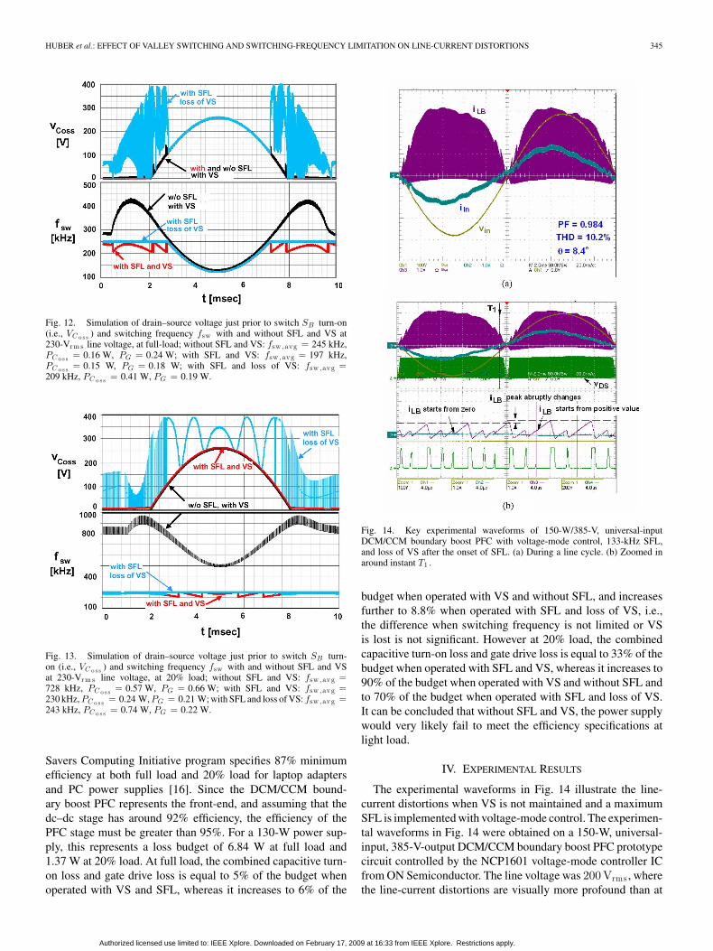
Fig. 10. Simulation subcircuit illustrating frequency limit and VS using theL6563 controller.
inductor, SIMPLIS simulations were performed. The simulationcircuit was a 130-W, universal-input, 385-V-output, DCM/CCMboundary boost PFC converter with LB = 230 µH and with250-kHz SFL, operating with current-mode control and VS. Thecontrol circuit is based on the L6563 controller from ST Micro-electronics. Since the L6563 controller does not have an internalSFL, the control circuit is simulated, as shown in Fig. 10. Thezero-current detect (ZCD) input of L6563 is connected throughan OR gate to monoflops 1 and 2, where monoflop 1 receivesa signal from a comparator monitoring the voltage of the aux-iliary winding of boost inductor LB , and produces a 100-nspulse when VS is maintained and a 4.1-µs pulse when VS isnot maintained. Monoflop 2 produces a 4-µs pulse when thegate drive signal goes high, which prevents the turn-on of mainswitch SB until a 4-µs minimum switching period has passed.VS is obtained by sensing the change in polarity of the volt-age across inductor LB and by implementing a short delay(i.e., 200 ns) internal to L6563. Since this delay is fixed, VScan be adjusted by adding a capacitor across main switch SB
in order to change the resonant interval to match the internaldelay. VS can be controlled in a more sophisticated way bysensing when the slope of the ringing voltage across the aux-iliary winding approaches zero [9]. It should be noted that the100-ns pulsewidth of monoflop 1 is shorter than a typical reso-nant interval, whereas the 4.1-µs pulsewidth guarantees properoperation even if the resonance becomes damped, and therefore,undetectable.
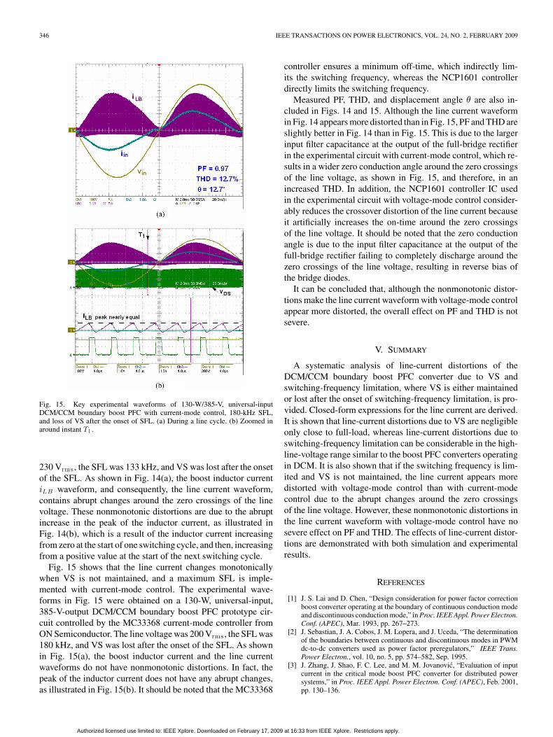
Fig. 11 shows simulation waveforms at 230-Vrms line voltageand at full load. The switching frequency variation during theentire line cycle is also included in Fig. 11. It is shown inFig. 11 that switching frequency fsw is not firmly clamped toits limit due to valley skipping, i.e., due to the fact that thecircuit must wait for the next resonant valley before turning on.It can be seen in Fig. 11 that a discontinuity occurs in the linecurrent waveform whenever switching frequency fsw reaches its250-kHz limit. For comparison with the case without SFL, thecorresponding line current waveform and switching frequencyvariation are also presented in Fig. 11. It should be noted thatin the case where the switching frequency is not limited by thecontrol circuit, it is nevertheless limited by the effect of the filtercapacitor at the output of the full-bridge rectifier, which preventsthe rectified line voltage to decrease to zero.
It follows from Fig. 11 that the line current waveform withSFL is more distorted than without SFL. Calculated PF andTHD values are also included in Fig. 11. It should be noted
Fig. 11. Simulation waveforms of DCM/CCM boundary boost PFC with andwithout SFL at 230-Vrm s line voltage, at full-load; without SFL: PF = 0.994,THD = 6.6%, fsw ,avg = 245 kHz; with SFL: PF = 0.974, THD = 21.6%,fsw ,avg = 197 kHz.
that the displacement angle between the line voltage and thefundamental component of the line current is θ = 5◦.
The benefit of limiting the switching frequency is reducedswitching loss, both the capacitive turn-on loss PCo s s and gatedrive loss PG of switch SB , as well as the core and copper lossesof the inductor. Using simulation, drain–source voltage vDS , amoment prior to switch SB turn-on (i.e., VCo s s ), can be sampledalong with switching frequency fsw and used to determine bothturn-on loss PCo s s and gate drive loss PG during a line periodTL , respectively, defined as
PCo s s =1
TL
∫ TL
0
12fsw (t)CossV
2Co s s
(t) dt (20)
and
PG = VGGQG1
TL
∫ TL
0fsw (t) dt (21)
where VGG is the gate drive voltage and QG is the total gatecharge. Simulation waveforms during a half-line cycle and cal-culation results are presented in Fig. 12 for three cases: withoutSFL with VS, and SFL fsw ,max = 250 kHz with and withoutVS. The simulation was performed at 230-Vrms line voltageand full load, i.e., 130 W (VGG = 15 V, Coss = 100 pF, andQG = 60 nC). Although gate drive loss PG is similar in allcases, capacitive turn-on loss PCo s s is nearly three times higherwhen VS is lost. However, performing a similar simulation at20% load (see Fig. 13) shows that gate drive loss PG nearlytriples when the frequency is not limited, and capacitive turn-onloss PCo s s nearly triples when VS is lost while operating withSFL. In addition to an increased loss, the effect of losing VS isalso an increase in conducted EMI [9], which may necessitateadditional filtration, which further increases the total loss.
The necessity of VS and switching-frequency limitation atlight loads can be further illustrated with loss calculations withrespect to the overall loss budget. For example, the Climate
Authorized licensed use limited to: IEEE Xplore. Downloaded on February 17, 2009 at 16:33 from IEEE Xplore. Restrictions apply.
HUBER et al.: EFFECT OF VALLEY SWITCHING AND SWITCHING-FREQUENCY LIMITATION ON LINE-CURRENT DISTORTIONS 345
Fig. 12. Simulation of drain–source voltage just prior to switch SB turn-on(i.e., VC o s s ) and switching frequency fsw with and without SFL and VS at230-Vrm s line voltage, at full-load; without SFL and VS: fsw ,avg = 245 kHz,PC o s s = 0.16 W, PG = 0.24 W; with SFL and VS: fsw ,avg = 197 kHz,PC o s s = 0.15 W, PG = 0.18 W; with SFL and loss of VS: fsw ,avg =209 kHz, PC o s s = 0.41 W, PG = 0.19 W.
Fig. 13. Simulation of drain–source voltage just prior to switch SB turn-on (i.e., VC o s s ) and switching frequency fsw with and without SFL and VSat 230-Vrm s line voltage, at 20% load; without SFL and VS: fsw ,avg =728 kHz, PC o s s = 0.57 W, PG = 0.66 W; with SFL and VS: fsw ,avg =230 kHz, PC o s s = 0.24 W, PG = 0.21 W; with SFL and loss of VS: fsw ,avg =243 kHz, PC o s s = 0.74 W, PG = 0.22 W.
Savers Computing Initiative program specifies 87% minimumefficiency at both full load and 20% load for laptop adaptersand PC power supplies [16]. Since the DCM/CCM bound-ary boost PFC represents the front-end, and assuming that thedc–dc stage has around 92% efficiency, the efficiency of thePFC stage must be greater than 95%. For a 130-W power sup-ply, this represents a loss budget of 6.84 W at full load and1.37 W at 20% load. At full load, the combined capacitive turn-on loss and gate drive loss is equal to 5% of the budget whenoperated with VS and SFL, whereas it increases to 6% of the
Fig. 14. Key experimental waveforms of 150-W/385-V, universal-inputDCM/CCM boundary boost PFC with voltage-mode control, 133-kHz SFL,and loss of VS after the onset of SFL. (a) During a line cycle. (b) Zoomed inaround instant T1 .
budget when operated with VS and without SFL, and increasesfurther to 8.8% when operated with SFL and loss of VS, i.e.,the difference when switching frequency is not limited or VSis lost is not significant. However at 20% load, the combinedcapacitive turn-on loss and gate drive loss is equal to 33% of thebudget when operated with SFL and VS, whereas it increases to90% of the budget when operated with VS and without SFL andto 70% of the budget when operated with SFL and loss of VS.It can be concluded that without SFL and VS, the power supplywould very likely fail to meet the efficiency specifications atlight load.
IV. EXPERIMENTAL RESULTS
The experimental waveforms in Fig. 14 illustrate the line-current distortions when VS is not maintained and a maximumSFL is implemented with voltage-mode control. The experimen-tal waveforms in Fig. 14 were obtained on a 150-W, universal-input, 385-V-output DCM/CCM boundary boost PFC prototypecircuit controlled by the NCP1601 voltage-mode controller ICfrom ON Semiconductor. The line voltage was 200Vrms , wherethe line-current distortions are visually more profound than at
Authorized licensed use limited to: IEEE Xplore. Downloaded on February 17, 2009 at 16:33 from IEEE Xplore. Restrictions apply.
346 IEEE TRANSACTIONS ON POWER ELECTRONICS, VOL. 24, NO. 2, FEBRUARY 2009
Fig. 15. Key experimental waveforms of 130-W/385-V, universal-inputDCM/CCM boundary boost PFC with current-mode control, 180-kHz SFL,and loss of VS after the onset of SFL. (a) During a line cycle. (b) Zoomed inaround instant T1 .
230 Vrms , the SFL was 133 kHz, and VS was lost after the onsetof the SFL. As shown in Fig. 14(a), the boost inductor currentiLB waveform, and consequently, the line current waveform,contains abrupt changes around the zero crossings of the linevoltage. These nonmonotonic distortions are due to the abruptincrease in the peak of the inductor current, as illustrated inFig. 14(b), which is a result of the inductor current increasingfrom zero at the start of one switching cycle, and then, increasingfrom a positive value at the start of the next switching cycle.
Fig. 15 shows that the line current changes monotonicallywhen VS is not maintained, and a maximum SFL is imple-mented with current-mode control. The experimental wave-forms in Fig. 15 were obtained on a 130-W, universal-input,385-V-output DCM/CCM boundary boost PFC prototype cir-cuit controlled by the MC33368 current-mode controller fromON Semiconductor. The line voltage was 200 Vrms , the SFL was180 kHz, and VS was lost after the onset of the SFL. As shownin Fig. 15(a), the boost inductor current and the line currentwaveforms do not have nonmonotonic distortions. In fact, thepeak of the inductor current does not have any abrupt changes,as illustrated in Fig. 15(b). It should be noted that the MC33368
controller ensures a minimum off-time, which indirectly lim-its the switching frequency, whereas the NCP1601 controllerdirectly limits the switching frequency.
Measured PF, THD, and displacement angle θ are also in-cluded in Figs. 14 and 15. Although the line current waveformin Fig. 14 appears more distorted than in Fig. 15, PF and THD areslightly better in Fig. 14 than in Fig. 15. This is due to the largerinput filter capacitance at the output of the full-bridge rectifierin the experimental circuit with current-mode control, which re-sults in a wider zero conduction angle around the zero crossingsof the line voltage, as shown in Fig. 15, and therefore, in anincreased THD. In addition, the NCP1601 controller IC usedin the experimental circuit with voltage-mode control consider-ably reduces the crossover distortion of the line current becauseit artificially increases the on-time around the zero crossingsof the line voltage. It should be noted that the zero conductionangle is due to the input filter capacitance at the output of thefull-bridge rectifier failing to completely discharge around thezero crossings of the line voltage, resulting in reverse bias ofthe bridge diodes.
It can be concluded that, although the nonmonotonic distor-tions make the line current waveform with voltage-mode controlappear more distorted, the overall effect on PF and THD is notsevere.
V. SUMMARY
A systematic analysis of line-current distortions of theDCM/CCM boundary boost PFC converter due to VS andswitching-frequency limitation, where VS is either maintainedor lost after the onset of switching-frequency limitation, is pro-vided. Closed-form expressions for the line current are derived.It is shown that line-current distortions due to VS are negligibleonly close to full-load, whereas line-current distortions due toswitching-frequency limitation can be considerable in the high-line-voltage range similar to the boost PFC converters operatingin DCM. It is also shown that if the switching frequency is lim-ited and VS is not maintained, the line current appears moredistorted with voltage-mode control than with current-modecontrol due to the abrupt changes around the zero crossingsof the line voltage. However, these nonmonotonic distortions inthe line current waveform with voltage-mode control have nosevere effect on PF and THD. The effects of line-current distor-tions are demonstrated with both simulation and experimentalresults.
REFERENCES
[1] J. S. Lai and D. Chen, “Design consideration for power factor correctionboost converter operating at the boundary of continuous conduction modeand discontinuous conduction mode,” in Proc. IEEE Appl. Power Electron.Conf. (APEC), Mar. 1993, pp. 267–273.
[2] J. Sebastian, J. A. Cobos, J. M. Lopera, and J. Uceda, “The determinationof the boundaries between continuous and discontinuous modes in PWMdc-to-dc converters used as power factor preregulators,” IEEE Trans.Power Electron., vol. 10, no. 5, pp. 574–582, Sep. 1995.
[3] J. Zhang, J. Shao, F. C. Lee, and M. M. Jovanovic, “Evaluation of inputcurrent in the critical mode boost PFC converter for distributed powersystems,” in Proc. IEEE Appl. Power Electron. Conf. (APEC), Feb. 2001,pp. 130–136.
Authorized licensed use limited to: IEEE Xplore. Downloaded on February 17, 2009 at 16:33 from IEEE Xplore. Restrictions apply.
HUBER et al.: EFFECT OF VALLEY SWITCHING AND SWITCHING-FREQUENCY LIMITATION ON LINE-CURRENT DISTORTIONS 347
[4] M. Shen, Z. Qian, and M. Chen, “Analysis and average modeling of criticalmode boost PFC converter,” in Proc. IEEE Power Electron. Drive Syst.Conf. (PEDS), Oct. 2001, pp. 138–141.
[5] M. Gotfryd, “Limits in boost power factor corrector operating in border-line mode,” IEEE Trans. Power Electron., vol. 18, no. 6, pp. 1330–1335,Nov. 2003.
[6] J. W. Kim, S. M. Choi, and K. T. Kim, “Variable on-time control ofthe critical conduction mode boost power factor correction converter toimprove zero-crossing distortion,” in Proc. IEEE Power Electron. DriveSyst. Conf. (PEDS), Nov. 2005, pp. 1542–1546.
[7] A. Abramovitz, “Effect of the ripple current on power factor of CRMboost APFC,” in Proc. CES/IEEE Int. Power Electron. Motion ControlConf. (IPEMC), Aug. 2006, pp. 1412–1415.
[8] Y.-K. Lo, J.-Y. Lin, and S.-Y. Ou, “Switching-frequency control for regu-lated discontinuous-conduction-mode boost rectifiers,” IEEE Trans. Ind.Electron., vol. 54, no. 2, pp. 760–768, Apr. 2007.
[9] W. Langeslag, R. Pagano, K. Schetters, A. Strijker, and A. Zoest, “VLSIdesign and application of a high-voltage-compatible SoC-ASIC in bipo-lar CMOS/DMOS technology for AC-DC rectifiers,” IEEE Trans. Ind.Electron., vol. 54, no. 5, pp. 2626–2641, Oct. 2007.
[10] L. Huber and M. M. Jovanovic, “Single-stage single-switch input currentshaping technique with reduced switching loss,” IEEE Trans. PowerElectron., vol. 15, no. 4, pp. 681–687, Jul. 2000.
[11] Y. Panov and M. M. Jovanovic, “Adaptive off-time control for variable-frequency, soft-switched flyback converter at light loads,” IEEE Trans.Power Electron., vol. 17, no. 4, pp. 596–603, Jul. 2002.
[12] M. M. Jovanovic and Y. Jang, “State-of-the-art, single-phase, active power-factor-correction techniques for high-power applications—An overview,”IEEE Trans. Ind. Electron., vol. 52, no. 3, pp. 701–708, Jun. 2005.
[13] K. H. Liu and Y. L. Lin, “Current waveform distortion in power factorcorrection circuits employing discontinuous-mode boost converters,” inProc. IEEE Power Electron. Spec. Conf. (PESC), Jun. 1989, pp. 825–829.
[14] D. S. L. Simonetti, J. L. F. Vieira, and G. C. D. Sousa, “Modeling ofthe high-power factor discontinuous boost rectifier,” IEEE Trans. Ind.Electron., vol. 46, no. 4, pp. 788–795, Aug. 1999.
[15] Environmental Protection Agency (EPA), “Energy Star Program Require-ments for Single Voltage External AC-DC and AC-AC Power Supplies,Eligibility Criteria (version 2.0),” [Online]. Available: http://www.energystar.gov/ia/partners/prod_development/revisions/downloads/eps_spec_v2.pdf
[16] “Climate Savers Computing Initiative,” White paper. (2008).[Online]. Available: http://www.climatesaverscomputing.org/media/White_Paper_11.25.08.pdf
[17] K. De Gusseme, D. M. Van de Sype, A. P. M. Van Den Bossche, andJ. A. Melkebeek, “Input-current distortion of CCM boost PFC convertersoperated in DCM,” IEEE Trans. Ind. Electron., vol. 54, no. 2, pp. 858–865,Apr. 2007.
[18] P. Preller, “A controller family for switch mode power supplies supportinglow power standby and power factor correction,” Infineon Technol. AG,Munich, Germany, Appl. Note AN-TDA 1684X, Jun. 2000.
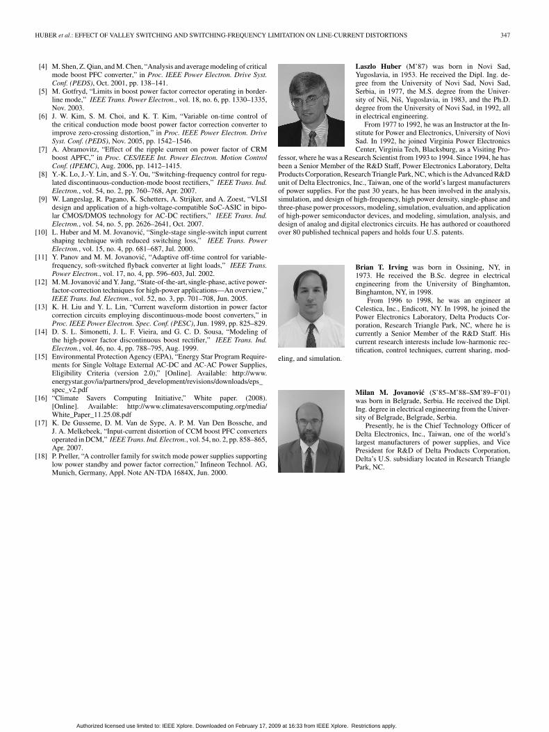
Laszlo Huber (M’87) was born in Novi Sad,Yugoslavia, in 1953. He received the Dipl. Ing. de-gree from the University of Novi Sad, Novi Sad,Serbia, in 1977, the M.S. degree from the Univer-sity of Nis, Nis, Yugoslavia, in 1983, and the Ph.D.degree from the University of Novi Sad, in 1992, allin electrical engineering.
From 1977 to 1992, he was an Instructor at the In-stitute for Power and Electronics, University of NoviSad. In 1992, he joined Virginia Power ElectronicsCenter, Virginia Tech, Blacksburg, as a Visiting Pro-
fessor, where he was a Research Scientist from 1993 to 1994. Since 1994, he hasbeen a Senior Member of the R&D Staff, Power Electronics Laboratory, DeltaProducts Corporation, Research Triangle Park, NC, which is the Advanced R&Dunit of Delta Electronics, Inc., Taiwan, one of the world’s largest manufacturersof power supplies. For the past 30 years, he has been involved in the analysis,simulation, and design of high-frequency, high power density, single-phase andthree-phase power processors, modeling, simulation, evaluation, and applicationof high-power semiconductor devices, and modeling, simulation, analysis, anddesign of analog and digital electronics circuits. He has authored or coauthoredover 80 published technical papers and holds four U.S. patents.
Brian T. Irving was born in Ossining, NY, in1973. He received the B.Sc. degree in electricalengineering from the University of Binghamton,Binghamton, NY, in 1998.
From 1996 to 1998, he was an engineer atCelestica, Inc., Endicott, NY. In 1998, he joined thePower Electronics Laboratory, Delta Products Cor-poration, Research Triangle Park, NC, where he iscurrently a Senior Member of the R&D Staff. Hiscurrent research interests include low-harmonic rec-tification, control techniques, current sharing, mod-
eling, and simulation.
Milan M. Jovanovic (S’85–M’88–SM’89–F’01)was born in Belgrade, Serbia. He received the Dipl.Ing. degree in electrical engineering from the Univer-sity of Belgrade, Belgrade, Serbia.
Presently, he is the Chief Technology Officer ofDelta Electronics, Inc., Taiwan, one of the world’slargest manufacturers of power supplies, and VicePresident for R&D of Delta Products Corporation,Delta’s U.S. subsidiary located in Research TrianglePark, NC.
Authorized licensed use limited to: IEEE Xplore. Downloaded on February 17, 2009 at 16:33 from IEEE Xplore. Restrictions apply.