how to drive gan enhancement mode power switching ... systems_gn001 app... · mode power switching...
TRANSCRIPT

APPLICATION NOTE
GN001 Rev 2014-10-21 © 2009 - 2014 GaN Systems Inc. 1
How to Drive GaN Enhancement Mode Power Switching Transistors
This application note sets out design guidelines and circuit layout considerations for the gate drive of GaN Systems enhancement mode power switching transistors. The first section covers basic principles and the following section shows a specific design example.
1. Principles of driver design
Gate characteristics The equivalent gate circuit of a typical GaN Systems enhancement mode HEMT (E-‐‑HEMT) is shown in Figure 1. The model consists of two capacitors (CGS and CGD), and an internal gate resistor RG,int. Full enhancement of the channel requires VGS = 7V and the absolute maximum limit of VGS is +/-‐‑10V. Excessive inductance in the gate loop can drive the voltage beyond the rated maximum, which must be avoided. As the inductance increases, so does the ringing and peak voltage. Compared to a Si MOSFET with similar size (on-‐‑state resistance), GaN systems E-‐‑HEMTs have:
a) Lower specified and peak gate voltage ratings, so a gate driver that is compatible with lower gate voltage operation is needed.
b) Much lower gate capacitance, meaning that the external gate resistor will typically have a much higher value. Combined with lower gate voltage, this also means significant lower gate drive power loss thus smaller and lower cost gate driver can be used. For example, GaN E-‐‑HEMT GS66508P has gate drive power loss about 17 times lower than state of art superjunction MOSFET (Coolmos IPP65R065C7) with equivalent Rds(on).
c) Lower transconductance, meaning that the gate should be driven close to the specified value, otherwise conduction losses will increase at higher currents.
d) A higher ratio of Miller capacitance (CGD) to gate capacitance (CGS). Having a relatively small CGS compared to the CGD means that the
Figure 1: Gate equivalent circuit
RG,int
CGS
Gate
Source
VGS
CGD
Drain

APPLICATION NOTE
GN001 Rev 2014-10-21 © 2009 - 2014 GaN Systems Inc. 2
switching speed can be better controlled as the Miller charge is controlled directly by the driver and is not damped by a large CGS.
Fast switching edges
Gallium nitride transistors are capable of switching at very high speed. The voltage slew rate may range from tens to hundreds of volts per nanosecond, and the current slew rate may be more than ten amps per nanosecond. Switching speed can be controlled by gate resistors. The following design guidelines should be used:
1) Design for as low inductance in the drain and source of the GaN transistor as possible.
2) Design for as low inductance in the gate drive circuitry as possible – the wider the traces and the shorter the gate drive loop the better. Choose a driver with a small outline surface-‐‑mount package designed for high speed operation.
3) There should be a ceramic capacitor between the driver VCC and the driver RTN – recommended value between 2.2µμF and 4.7µμF. This capacitor actually drives the transistor and needs to be placed as close to the driver and the transistor as possible. An additional de-‐‑coupling capacitor 0.1nF can be placed in parallel.
4) In order to minimize capacitive and inductive coupling the gate driving circuitry should be as far from the drain as possible. At the same time, the driving circuitry needs to be as close to the gate/source as possible – this minimizes the gate drive inductance which allows faster driving and lowers the gate to source voltage ringing.
Low impedance gate drive Another consequence of the high slew rate is that it may cause high current IGD to flow in the Miller capacitance (CGD). If the driver is not properly designed this effect may cause the device to spuriously turn on when it is intended to be off. In a typical half bridge topology application as shown in Figure 2, the low side transistor QL is susceptible to cross conduction (or shoot-‐‑through) while high side transistor QH is being turned on if the induced gate voltage VGL is higher than the gate threshold voltage. This increased risk of shoot-‐‑through current is a potential cause of
+ VDD
QH
QL
LO
CO
+ VO
RDRV(DOWN)
RG
CGD
CGS
LG
VSW
IGD
VGL
VGH
VGH
VSW
VGL
Figure 2: Low impedance drive circuit

APPLICATION NOTE
GN001 Rev 2014-10-21 © 2009 - 2014 GaN Systems Inc. 3
unwanted losses and may damage the device by exceeding its safe ratings. Therefore it is important to select a driver that not only meets the drive and speed requirements but also provides a low impedance path (low pull-‐‑down resistance RDRV(DOWN)) for the stray current caused by the high dv/dt, as illustrated in Figure 2. Below are the general gate drive design tips for preventing cross conduction:
• Minimize the gate loop inductance LG by locating the driver as close to gate and source-‐‑sense pads as possible.
• Select a driver that has low pull-‐‑down output impedance. • If gate resistor is used for slew rate control, consider using separate turn-‐‑off
gate resistor to minimize the impedance during turn-‐‑off. • Optimize the turn-‐‑on speed to limit the dv/dt. • More advanced techniques, such as “Active Miller Clamping”, may be used
to provide a low impedance path without compromising the turn-‐‑off slew rate control. Although some gate driver ICs have an integrated Active Miller Clamping function, most of them are not compatible with a 7V gate drive voltage. Instead a discrete method of adding a PNP transistor [1] can be implemented to bypass Miller current and provide a low impedance path during turning-‐‑off.
Gate resistors The slew rate of a GaN Systems E-‐‑HEMT can be easily controlled by using a gate resistor. The following are general recommendations for selecting gate resistors:
• Start with a turn-‐‑on gate resistor between 10 and 20Ω, which results in approximately 40-‐‑80V/ns dv/dt slew rate for the GS66508P. The value can then be adjusted empirically to achieve the desired slew rate.
• A smaller turn-‐‑off resistor can be used for better immunity to cross conduction. If the driver does not support a separate turn-‐‑off resistor, use a diode in parallel as shown in Figure 3. Having a much smaller gate charge means a significantly lower gate drive power loss so a smaller surface mount resistor such as 0603 can be used for the gate resistors, which also allows the driver to be placed closer to the gate and thus provides a tighter gate loop layout.
• The values for gate resistors need to be optimized based on the specific application requirements (switching loss, EMI and overshoot).
D
G
SS S
RG1
RG2D1
OUT
VDRV_RTN
Figure 3: Separate turn-off resistor
APPLICATION NOTE
GN001 Rev 2014-10-21 © 2009 - 2014 GaN Systems Inc. 4
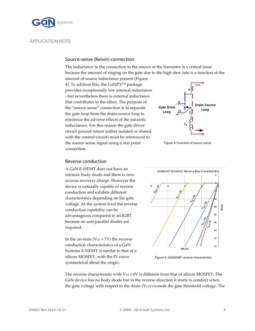
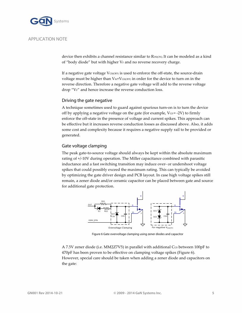
Source-sense (Kelvin) connection The inductance in the connection to the source of the transistor is a critical issue because the amount of ringing on the gate due to the high slew rate is a function of the amount of source inductance present (Figure 4). To address this, the GaNPX™ package provides exceptionally low internal inductance -‐‑ but nevertheless there is external inductance that contributes to the effect. The purpose of the “source sense” connection is to separate the gate loop from the drain-‐‑source loop to minimize the adverse effects of the parasitic inductances. For this reason the gate driver circuit ground return (either isolated or shared with the control circuit) must be referenced to the source-‐‑sense signal using a star point connection. Reverse conduction A GaN E-‐‑HEMT does not have an intrinsic body diode and there is zero reverse recovery charge. However the device is naturally capable of reverse conduction and exhibits different characteristics depending on the gate voltage. At the system level the reverse conduction capability can be advantageous compared to an IGBT because no anti-‐‑parallel diodes are required. In the on-‐‑state (VGS = 7V) the reverse conduction characteristics of a GaN Systems E-‐‑HEMT is similar to that of a silicon MOSFET, with the IV curve symmetrical about the origin. The reverse characteristic with VGS ≤ 0V is different from that of silicon MOSFET. The GaN device has no body diode but in the reverse direction it starts to conduct when the gate voltage with respect to the drain (VGD) exceeds the gate threshold voltage. The
Figure 5: GS66508P reverse characteristic
D
G
SSS
LS
Gate Drive Loop
Drain-‐Source Loop
Figure 4: Function of source sense
APPLICATION NOTE
GN001 Rev 2014-10-21 © 2009 - 2014 GaN Systems Inc. 5
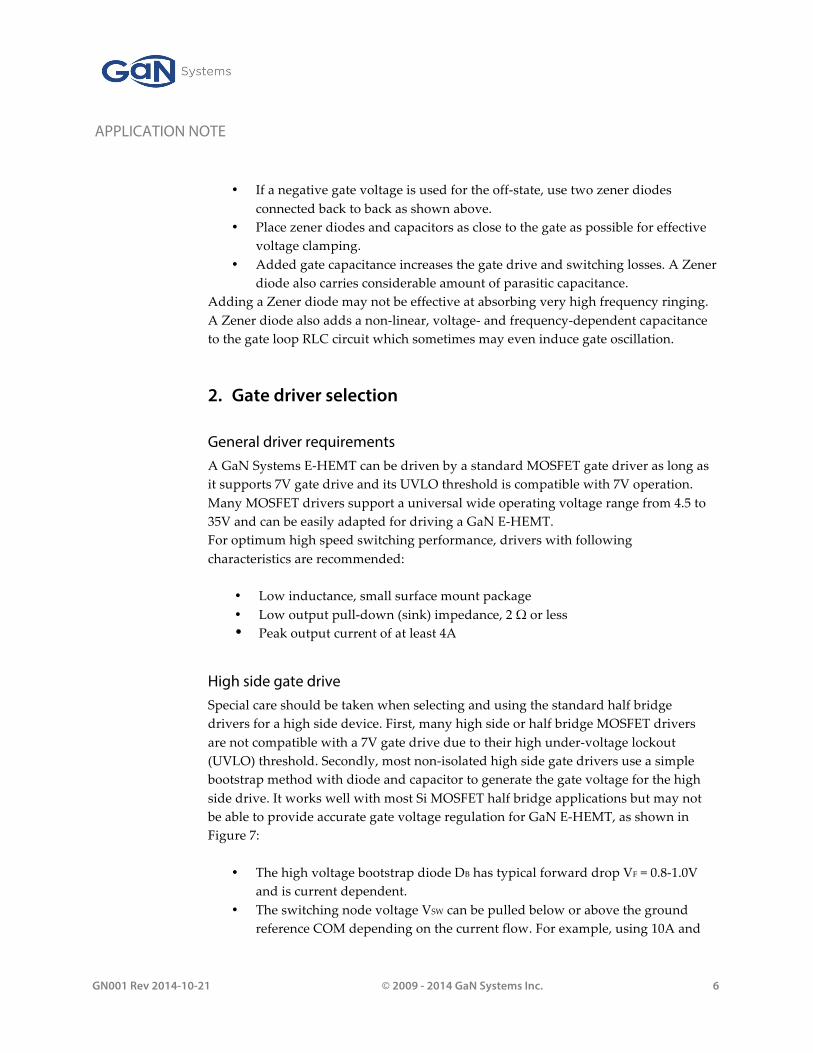
device then exhibits a channel resistance similar to RDS(ON). It can be modeled as a kind of “body diode” but with higher VF and no reverse recovery charge. If a negative gate voltage VGS(OFF) is used to enforce the off-‐‑state, the source-‐‑drain voltage must be higher than Vth+VGS(OFF) in order for the device to turn on in the reverse direction. Therefore a negative gate voltage will add to the reverse voltage drop “VF” and hence increase the reverse conduction loss. Driving the gate negative A technique sometimes used to guard against spurious turn-‐‑on is to turn the device off by applying a negative voltage on the gate (for example, VGS = -‐‑2V) to firmly enforce the off-‐‑state in the presence of voltage and current spikes. This approach can be effective but it increases reverse conduction losses as discussed above. Also, it adds some cost and complexity because it requires a negative supply rail to be provided or generated. Gate voltage clamping The peak gate-‐‑to-‐‑source voltage should always be kept within the absolute maximum rating of +/-‐‑10V during operation. The Miller capacitance combined with parasitic inductance and a fast switching transition may induce over-‐‑ or undershoot voltage spikes that could possibly exceed the maximum rating. This can typically be avoided by optimizing the gate driver design and PCB layout. In case high voltage spikes still remain, a zener diode and/or ceramic capacitor can be placed between gate and source for additional gate protection.
Figure 6 Gate overvoltage clamping using zener diodes and capacitor
A 7.5V zener diode (i.e. MM2Z7V5) in parallel with additional CGS between 100pF to 470pF has been proven to be effective on clamping voltage spikes (Figure 6). However, special care should be taken when adding a zener diode and capacitors on the gate:
D
G
SS S
RG1
RG2D1
OUT
VDRV_RTN
DZ1CGS7.5V
D
G
SS SCGS
DZ1
DZ2
Overvoltage Clamping For negative VGS(OFF)
APPLICATION NOTE
GN001 Rev 2014-10-21 © 2009 - 2014 GaN Systems Inc. 6
• If a negative gate voltage is used for the off-‐‑state, use two zener diodes connected back to back as shown above.
• Place zener diodes and capacitors as close to the gate as possible for effective voltage clamping.
• Added gate capacitance increases the gate drive and switching losses. A Zener diode also carries considerable amount of parasitic capacitance.
Adding a Zener diode may not be effective at absorbing very high frequency ringing. A Zener diode also adds a non-‐‑linear, voltage-‐‑ and frequency-‐‑dependent capacitance to the gate loop RLC circuit which sometimes may even induce gate oscillation.
2. Gate driver selection General driver requirements A GaN Systems E-‐‑HEMT can be driven by a standard MOSFET gate driver as long as it supports 7V gate drive and its UVLO threshold is compatible with 7V operation. Many MOSFET drivers support a universal wide operating voltage range from 4.5 to 35V and can be easily adapted for driving a GaN E-‐‑HEMT. For optimum high speed switching performance, drivers with following characteristics are recommended:
• Low inductance, small surface mount package • Low output pull-‐‑down (sink) impedance, 2 Ω or less • Peak output current of at least 4A
High side gate drive
Special care should be taken when selecting and using the standard half bridge drivers for a high side device. First, many high side or half bridge MOSFET drivers are not compatible with a 7V gate drive due to their high under-‐‑voltage lockout (UVLO) threshold. Secondly, most non-‐‑isolated high side gate drivers use a simple bootstrap method with diode and capacitor to generate the gate voltage for the high side drive. It works well with most Si MOSFET half bridge applications but may not be able to provide accurate gate voltage regulation for GaN E-‐‑HEMT, as shown in Figure 7:
• The high voltage bootstrap diode DB has typical forward drop VF = 0.8-‐‑1.0V and is current dependent.
• The switching node voltage VSW can be pulled below or above the ground reference COM depending on the current flow. For example, using 10A and

APPLICATION NOTE
GN001 Rev 2014-10-21 © 2009 - 2014 GaN Systems Inc. 7
50mΩ Rds(on), the switching node voltage can swing from -‐‑2.5V when current flows in reverse conduction to +0.5V for forward conduction. This results in more than +/-‐‑20% change (5.5 – 8.5V) on the bootstrap voltage.
• In addition to static voltage drop, parasitic inductance also creates a negative “below ground” undershoot voltage spike on VSW under high di/dt switching transition.
Figure 7 Issue with bootstrap voltage regulation for high side gate drive
Although a GaN E-‐‑HEMT can still be driven with a lower gate voltage, such as 5V in the example given, the device channel will not be fully enhanced and thus there will be a higher conduction loss. One possible solution is to use a higher input voltage (12V) and add post regulation using an LDO voltage regulator after the bootstrap diode. Alternatively a floating isolated gate driver can be used for the high side gate drive. Isolated gate drive A discrete digital isolator in conjunction with an isolated power supply, or an integrated isolated driver chip, can be used to provide full galvanic isolation between the input and driver output stage. Follow the tips below when designing the isolated gate driver:
+ VDD
Half Bridge Gate Driver
COM
LO
CB
DB
VS
QH
VCC
HIN
LIN QL
HORG1
RG2
+ 7V 0.8-‐1.0V
VDD VB
IQL
RDS(ON) ~ = 50mΩ
+ -‐
VOUT
CO
VSW
VBOOT VBOOT -‐ VSWVSW -‐ COMIQL
5.5V+ 0.5V10A
COM
8.5V-‐2.5V-‐10A
APPLICATION NOTE
GN001 Rev 2014-10-21 © 2009 - 2014 GaN Systems Inc. 8
• Select an isolator that matches or exceeds following specifications: - High common mode transient immunity and low input-‐‑output parasitic capacitance (CIO ≤ 2pF). This is particularly critical for high side driving as the switch node voltage can have very high dv/dt slew rate.
- Active low state output. If device has a fail-‐‑safe or ULVO mode, ensure that it latches the output to low state during the protection mode.
• Minimize the inter-‐‑winding parasitic capacitance when designing or selecting the isolated power supply.
• The PCB layout is critical: avoid placing traces and ground plane under the isolator to minimize the stray capacitance on the board across the isolation barrier.
3. Gate driver example Figure 8 shows an example of an isolated gate driver circuit for 650V GaN E-‐‑HEMT. It was designed for a double pulse testing board and has been tested up to 600V and 40A switching in a half bridge configuration. The full bill of materials can be found in Table 1. Gate Driver IC U5 is single 9A high speed low side gate driver IXDN609SI. Alternatively TC4422, FAN3122 or other drivers that are compatible with a 7V gate drive can be used. Gate resistors RG1 and RG2 values are for reference only and can be adjusted for slew rate control. To minimize gate loop inductance, place U5 and RG1/RG2 as close to G and SS pads as possible. R5/C9 and D1 form a rising edge delay circuit and are optional for dead time control. Isolator Si8410 is used for digital signal isolation. Alternatively Si8610 or other high speed isolators with equivalent or better specification can be used. If a standard 50Ω impedance output is connected to the gate drive PWM input, a 50Ω impedance matching resistor should be added between PWM_IN and PWM_RTN. Additional ferrite beads or common mode choke may be added between PWM input and U4 to suppress noise and excess ringing if needed. Isolated Power Supply The gate driver power supply is isolated by U2 which converts the +5V to a +9V isolated output. U1 is a 100mA low drop out voltage regulator and its output is set by R1 and R2 to provide a +7V gate driving voltage. The digital isolator also requires +5V on the isolated side and it is powered by U3 (LDO 5V fixed output 50mA).

APPLICATION NOTE
GN001 Rev 2014-10-21 © 2009 - 2014 GaN Systems Inc. 9
Figu
re 8
: G
aN E
-HEM
T G
ate
Driv
er E
xam
ple

APPLICATION NOTE
GN001 Rev 2014-10-21 © 2009 - 2014 GaN Systems Inc. 10
Bill of Materials
Reference Quantity Description Manufacturer Manufacturer P/N
C1,C6,C11 3 CAP CER 0.22UF 35V 20% X7R 0603 TDK C1608X7R1V224M080AB
C2,C8,C13 3 CAP CER 1UF 25V 10% X7R 0805 KEMET C0805C105K3RACAUTO
C3,C4 2 CAP CER 10UF 10V 10% X7R 0805 KEMET C0805C106K8RACTU
C5 1 CAP CER 10UF 16V 10% X7R 1206 KEMET C1206C106K4RACTU
C7,C10 2 CAP CER 4.7UF 16V 10% X5R 1206 KEMET C1206C475K4PACTU
C9 1 CAP CER 100PF 50V 5% NP0 0603 KEMET C0603C101J5GACTU
C12 1 CAP CER 22PF 25V 5% NP0 0603 KEMET C0603C220J3GACAUTO
D1 1 DIODE SCHOTTKY 30V 0.03A SOD523 DIODES INC SDM03U40-7
Q1 1 GAN TRANS E-MODE 650V 34A GANPX GAN SYSTEMS GS66508P
RG1,RG2 2 RES 20R 1/10W 1% SMD 0603 VISHAY DALE CRCW060320R0FKEA
R1 1 RES 24.9K 1/10W 1% SMD 0603 VISHAY DALE CRCW060324K9FKEA
R2 1 RES 10K 1/10W 1% SMD 0603 VISHAY DALE CRCW060310K0FKEA
R3 1 RES 392R 1/2W 1% SMD 1206 STACKPOLE RNCP1206FTD392R
R4 1 RES 49R9 1/10W 1% SMD 0603 VISHAY DALE CRCW060349R9FKEA
R5 1 RES 1K00 1/10W 1% SMD 0603 VISHAY DALE CRCW06031K00FKEA
T1 1 COMMON MODE CHOKE 830UH 5.2A T/H 4PIN
RECOM POWER CMC-08
U1 1 IC REG LDO ADJ 100MA SOT89-5 TOREX XC6216C202PR-G U2 1 DC/DC CONV 5V-9V ISO 2W SIP-7 MURATA MEJ2S0509SC
U3 1 IC REG LDO 5V 50MA SC70-5 TEXAS INSTR TPS71550DCKR
U4 1 IC DIG ISOLATOR 1CH SOIC-8 SILICON LAB SI8410BB-D-IS
U5 1 IC GATE DRIVER 9A N-INV SOIC-8 IXYS IXDN609SI
Table 1: Gate driver bill of materials

APPLICATION NOTE
GN001 Rev 2014-10-21 © 2009 - 2014 GaN Systems Inc. 11
PCB Layout Figure 9 depicts an example of a gate driver layout in a half bridge application. The gate driver U5 and the gate resistors RG are placed next to the gate and source-‐‑sense pins to minimize the gate loop inductance. C10 is the bypass capacitor that supplies the gate driving current so it must be located as close to U5 as possible. In this example C10 is placed at the bottom side, directly underneath the driver U5 VCC pin.
Figure 9 Example of Gate Driver PCB Layout (half bridge, top side)
Figure 10: Example of Gate Driver PCB Layout (bottom side) Figure 10 shows the bottom side of the PCB. For optimum performance the device thermal pad (substrate) is connected to the source by a copper plane on the bottom layer. A heatsink is attached to the PCB underneath the thermal pad. The gate driver ground plane (GND_GD) is referenced to the source-‐‑sense pad. Wide traces and multiple vias are used to provide a low impedance path from the power supply output to C10 and to the U5 VCC pin.

APPLICATION NOTE
GN001 Rev 2014-10-21 © 2009 - 2014 GaN Systems Inc. 12
Switching waveforms The gate driver circuits have been tested on a double pulse testing evaluation board and typical switching waveforms are shown in Figure 11 and Figure 12. The input voltage is 400VDC and the switching current is 33A. With a 10Ω gate resistor, this gate driver is capable of switching a single GaN transistor (GS66508P) at a dv/dt slew rate close to 80V/ns with a clean gate voltage waveform and minimal ringing during the switching transient.
Figure 11: Turn on waveforms (GS66508P, 400V/33A, RG_ON = 10Ω)
Figure 12: Turn off waveforms (GS66508P , 400V/33A, RG_OFF = 10Ω)

APPLICATION NOTE
GN001 Rev 2014-10-21 © 2009 - 2014 GaN Systems Inc. 13
Summary
This note has outlined the circuit design and layout factors that should be considered when designing drive circuitry for GaN Systems very high performance enhancement mode power switching transistors. It has described a particular reference design illustrating these considerations, including bill of materials and PCB layout. Reference
1. Fairchild Semi., Appl. note AN-‐‑5073 “Active Miller Clamp Technology”, 2013
www.gansystems.com North America � Europe � Asia
Important Notice – Unless expressly approved in writing by an authorized representative of GaN Systems, GaN Systems components are not designed, authorized or warranted for use in lifesaving, life sustaining, military, aircraft, or space applications, nor in products or systems where failure or malfunction may result in personal injury, death, or property or environmental damage. The information given in this document shall not in any event be regarded as a guarantee of performance. GaN Systems hereby disclaims any or all warranties and liabilities of any kind, including but not limited to warranties of non-infringement of intellectual property rights. All other brand and product names are trademarks or registered trademarks of their respective owners. Information provided herein is intended as a guide only and is subject to change without notice. The information contained herein or any use of such information does not grant, explicitly, or implicitly, to any party any patent rights, licenses, or any other intellectual property rights. GaN Systems standard terms and conditions apply. © 2009-2014 GaN Systems Inc. All rights reserved.