hms81c1808b/16b hms81c1708b/16b hms81c1608b/16b
TRANSCRIPT
ABOV SEMICONDUCTOR 8-BIT SINGLE-CHIP MICROCONTROLLERS
HMS81C1808B/16BHMS81C1708B/16BHMS81C1608B/16BHMS81C1508B/16B
HMS81C1404B/08B/16B
User’s Manual (Ver. 1.20)
Version 1.20
Published byFAE Team
©2006 ABOV Semiconductor Ltd. All right reserved.
Additional information of this manual may be served by ABOV Semiconductor offices in Korea or Distributors and Representatives.
ABOV Semiconductor reserves the right to make changes to any information here in at any time without notice.
The information, diagrams and other data in this manual are correct and reliable; however, ABOV Semiconductor is in no way responsiblefor any violations of patents or other rights of the third party generated by the use of this manual.
REVISION HISTORYVERSION 1.20 (April 2, 2008) This book
Corrected PSW(NVGBHIZC) for “INC A” instruction from N-----Z- to N-----ZC at " Arithmetic / Logic Operation" on page iv.VERSION 1.1 (MAR. 2006)
The company name, MagnaChip Semiconductor Ltd. changed to ABOV Semiconductor Co., Ltd..
VERSION 1.05 (OCT. 2005)
Correct the circuit connection condition in case of internal 4MHz oscillation.
Add internal oscillation frequency tolerance in DC Electrical Characteristics
Add notes in STOP operation and internal 4MHz oscillation.
VERSION 1.04 (JUN. 2005)
Add Pb free package
VERSION 1.03 (MAR. 2005)
Add read-modify-write chapter.
Correct the internal 4MHz oscillation clock period accuracy
VERSION 1.02 (SEP. 2004)
The company name, Hynix Semiconductor Inc. changed to MagnaChip Semiconductor Ltd.
VERSION 1.01 (MAR. 2004)
Correct the external RC oscillation characteristics.Fixed some errata.
HMS81C1404B/08B/16B/1508B/1516B/1608B/1616B/1708B/1716B/1808B/1816B
1. OVERVIEW......................................................... 1Description ........................................................ 1Features............................................................ 1Development Tools ........................................... 2Ordering Information.................................. 2
2. BLOCK DIAGRAM ............................................. 33. PIN ASSIGNMENT ............................................. 44. PACKAGE DRAWING........................................ 65. PIN FUNCTION................................................... 96. PORT STRUCTURES....................................... 117. ELECTRICAL CHARACTERISTICS................ 17
Absolute Maximum Ratings ............................ 17Recommended Operating Conditions............. 17A/D Converter Characteristics ........................ 17DC Electrical Characteristics .......................... 18AC Characteristics .......................................... 19Typical Characteristics.................................... 20
8. MEMORY ORGANIZATION ............................. 23Registers......................................................... 23Program Memory ............................................ 25Data Memory .................................................. 28Addressing Mode ............................................ 32
9. I/O PORTS........................................................ 36RA and RAIO registers ................................... 36RB and RBIO registers ................................... 37RC and RCIO registers ................................... 39RD and RDIO registers ................................... 40RE and REIO registers ................................... 40Read-modify-write Feature ............................. 41
10. CLOCK GENERATOR ................................... 43Oscillation Circuit ............................................ 43
11. Basic Interval Timer ..................................... 4512. TIMER / COUNTER ........................................ 46
8-bit Timer/Counter Mode ............................... 4716-bit Timer/Counter Mode ............................. 488-bit Compare Output (16-bit) ......................... 498-bit Capture Mode ......................................... 49
16-bit Capture Mode ...................................... 52PWM Mode .................................................... 52
13. Serial Peripheral Interface........................... 5514. Buzzer Output function................................ 5715. ANALOG TO DIGITAL CONVERTER........... 5816. INTERRUPTS ................................................ 61
Interrupt Sequence......................................... 63BRK Interrupt ................................................. 64Multi Interrupt ................................................. 64External Interrupt............................................ 66
17. WATCHDOG TIMER...................................... 6818. Power Saving Mode ..................................... 69
Stop Mode...................................................... 69STOP Mode using Internal RCWDT .............. 71Wake-up Timer Mode..................................... 72Minimizing Current Consumption ................... 73
19. RESET ........................................................... 7520. POWER FAIL PROCESSOR......................... 7721. COUNTERMEASURE OF NOISE ................. 79
Oscillation Noise Protector............................. 79Oscillation Fail Processor............................... 80Examples of ONP........................................... 80
22. MASK Option ................................................ 81A. INSTRUCTION .................................................. ii
Terminology List................................................. iiInstruction Map.................................................. iiiInstruction Set ................................................... iv
B. MASK ORDER SHEET(HMS81C1404B).......... xC. MASK ORDER SHEET(HMS81C1408B)......... xiD. MASK ORDER SHEET(HMS81C1416B)........ xiiE. MASK ORDER SHEET(HMS81C1508B)....... xiiiF. MASK ORDER SHEET(HMS81C1516B) ....... xivG. MASK ORDER SHEET(HMS81C1608B) ....... xvH. MASK ORDER SHEET(HMS81C1616B)....... xviI. MASK ORDER SHEET(HMS81C1708B) ....... xviiJ. MASK ORDER SHEET(HMS81C1716B) ..... xviiiK. MASK ORDER SHEET(HMS81C1808B)....... xixL. MASK ORDER SHEET(HMS81C1816B) ........ xx
April 2, 2008 Ver 1.20 1

HMS81C1404B/08B/16B/1508B/1516B/1608B/1616B/1708B/1716B/1808B/1816B
2 April 2, 2008 Ver 1.20
HMS81C1404B/08B/16B/1508B/1516B/1608B/1616B/1708B/1716B/1808B/1816B
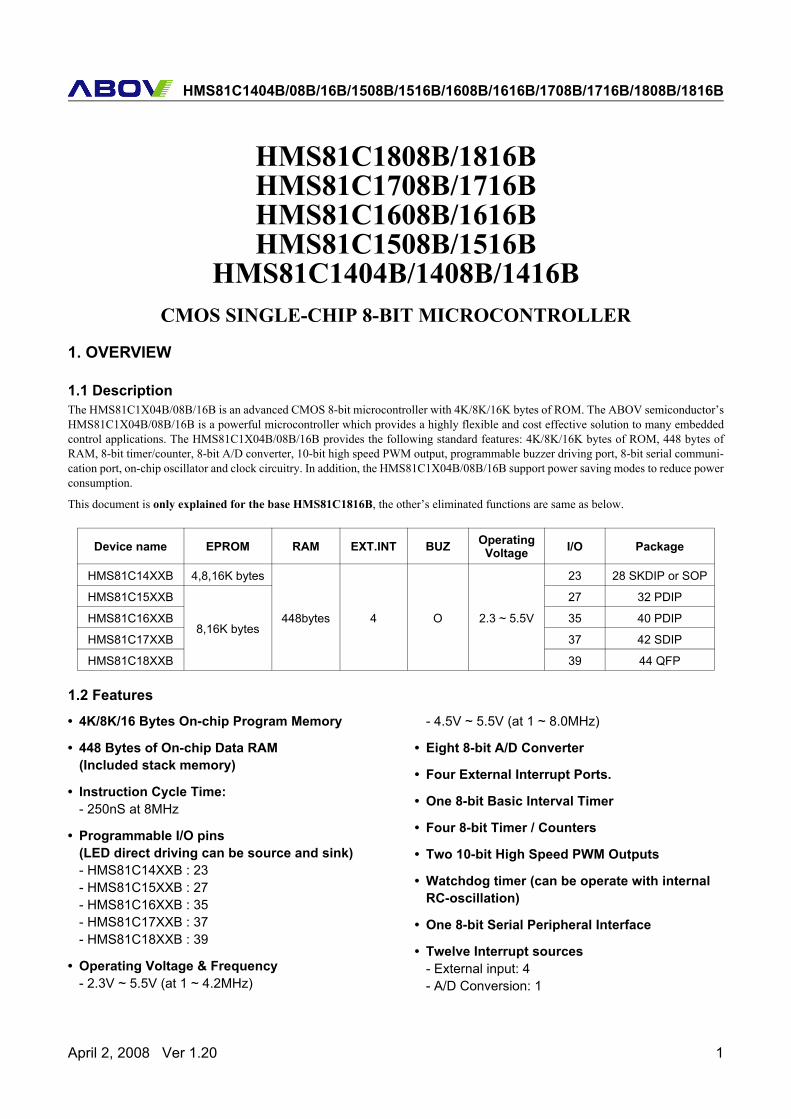
HMS81C1808B/1816BHMS81C1708B/1716BHMS81C1608B/1616BHMS81C1508B/1516B
HMS81C1404B/1408B/1416BCMOS SINGLE-CHIP 8-BIT MICROCONTROLLER
1. OVERVIEW
1.1 DescriptionThe HMS81C1X04B/08B/16B is an advanced CMOS 8-bit microcontroller with 4K/8K/16K bytes of ROM. The ABOV semiconductor’sHMS81C1X04B/08B/16B is a powerful microcontroller which provides a highly flexible and cost effective solution to many embeddedcontrol applications. The HMS81C1X04B/08B/16B provides the following standard features: 4K/8K/16K bytes of ROM, 448 bytes ofRAM, 8-bit timer/counter, 8-bit A/D converter, 10-bit high speed PWM output, programmable buzzer driving port, 8-bit serial communi-cation port, on-chip oscillator and clock circuitry. In addition, the HMS81C1X04B/08B/16B support power saving modes to reduce powerconsumption.
This document is only explained for the base HMS81C1816B, the other’s eliminated functions are same as below.
1.2 Features
• 4K/8K/16 Bytes On-chip Program Memory
• 448 Bytes of On-chip Data RAM(Included stack memory)
• Instruction Cycle Time:- 250nS at 8MHz
• Programmable I/O pins(LED direct driving can be source and sink)- HMS81C14XXB : 23- HMS81C15XXB : 27- HMS81C16XXB : 35- HMS81C17XXB : 37- HMS81C18XXB : 39
• Operating Voltage & Frequency- 2.3V ~ 5.5V (at 1 ~ 4.2MHz)
- 4.5V ~ 5.5V (at 1 ~ 8.0MHz)
• Eight 8-bit A/D Converter
• Four External Interrupt Ports.
• One 8-bit Basic Interval Timer
• Four 8-bit Timer / Counters
• Two 10-bit High Speed PWM Outputs
• Watchdog timer (can be operate with internal RC-oscillation)
• One 8-bit Serial Peripheral Interface
• Twelve Interrupt sources- External input: 4- A/D Conversion: 1
Device name EPROM RAM EXT.INT BUZ Operating Voltage I/O Package
HMS81C14XXB 4,8,16K bytes
448bytes 4 O 2.3 ~ 5.5V
23 28 SKDIP or SOP
HMS81C15XXB
8,16K bytes
27 32 PDIP
HMS81C16XXB 35 40 PDIP
HMS81C17XXB 37 42 SDIP
HMS81C18XXB 39 44 QFP
April 2, 2008 Ver 1.20 1
HMS81C1404B/08B/16B/1508B/1516B/1608B/1616B/1708B/1716B/1808B/1816B
- Serial Peripheral Interface: 1- Timer: 6
• One Programmable Buzzer Driving port- 500Hz ~ 130kHz
• Noise Immunity Circuit - Power Fail Processor- Oscillation Noise Protector- Oscillation Fail Processor
• Oscillator Type- Crystal- Ceramic Resonator
- RC Oscillator ( C can be omitted )- Internal Oscillator ( approx. 4MHz )
• Power Down Mode- STOP mode- Wake-up Timer mode- Internal RC Watchdog Timer mode
• Package Types- 28 SKDIP or SOP- 32 PDIP, 40 PDIP, 42 SDIP or 44 QFP- Avalilable Pb free package
1.3 Development ToolsThe HMS81C1X04B/08B/16B are supported by a full-featuredmacro assembler, an in-circuit emulator CHOICE-DrTM.
The macro assembler operates under the MS-Windows 95/98,2000, XPTM.
1.4 Ordering Information
Pb free package :
The “P” suffix will be added at the original part number. For example; HMS81C1416B SK (Normal package), HMS81C1416B SK P (Pb free package)
In Circuit Emulators CHOICE-Dr. TM
Assembler ABOV Macro Assembler
C compiler ABOV 800C compiler
ROM Size Package Type Ordering Device Code Operating Temperature
4K bytes (Mask) 28 SKDIP HMS81C1404B SK
-40 ~ +85°C
28 SOP HMS81C1404B D
8K bytes (Mask)
28 SKDIP HMS81C1408B SK 28 SOP HMS81C1408B D 32 PDIP HMS81C1508B 40 PDIP HMS81C1608B 42 SDIP HMS81C1708B K 44 MQFP HMS81C1808B Q
16K bytes (Mask)
28 SKDIP HMS81C1416B SK 28 SOP HMS81C1416B D 32 PDIP HMS81C1516B 40 PDIP HMS81C1616B 42 SDIP HMS81C1716B K 44 MQFP HMS81C1816B Q
2 April 2, 2008 Ver 1.20
HMS81C1404B/08B/16B/1508B/1516B/1608B/1616B/1708B/1716B/1808B/1816B
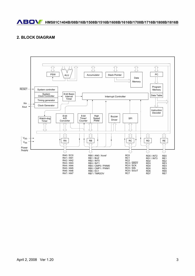
2. BLOCK DIAGRAM
ALU Accumulator Stack Pointer
Interrupt Controller
DataMemory
8-bit
ConverterA/D
8-bit
CounterTimer/
ProgramMemory
Data Table
PC
8-bit Basic
TimerInterval
Watch-dogTimer
Instruction
RA RB RC
BuzzerDriver
PSW
System controller
Timing generator
SystemClock Controller
Clock Generator
RESET
XinXout
RA0 / EC0RA1 / AN1RA2 / AN2RA3 / AN3RA4 / AN4RA5 / AN5RA6 / AN6RA7 / AN7
RB0 / AN0 / AvrefRB1 / BUZRB2 / INT0RB3 / INT1RB4 / CMP0 / PWM0
RC3 / SRDYRC4 / SCK
VDD
VSS
PowerSupply
DecoderHigh
PWMSpeed
RB5 / CMP1 / PWM1RB6 / EC1RB7 / TMR2OV
RC5 / SINRC6 / SOUT
RD
RD0 / INT2RD1 / INT3RD2
SPI
RC0RC1RC2
RC7
RD3RD4RD5RD6RD7
RE
RE0RE1RE2RE3RE4RE5RE6RE7
April 2, 2008 Ver 1.20 3
HMS81C1404B/08B/16B/1508B/1516B/1608B/1616B/1708B/1716B/1808B/1816B
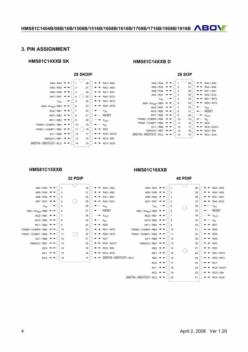
3. PIN ASSIGNMENT
RC4 / SCKSRDYIN / SRDYOUT / RC3
RC5 / SINTMR2OV / RB7
RA2 / AN2
RA1 / AN1
RA0 / EC0
RD1 / INT3
RD0 / INT2
VSS
RESET
XOUT
XIN
AN5 / RA5
AN6 / RA6
AN7 / RA7
VDD
AN0 / AVREF/ RB0
BUZ / RB1
28 SKDIP
2
3
4
5
6
7
8
9
10
27
26
25
24
23
22
21
20
19
11
12
RD2
RC6 / SOUT
18
17
RA3 / AN3RA2 / AN2RA1 / AN1RA0 / EC0RD1 / INT3
RD0 / INT2
VSS
RESETXOUTXIN
AN4 / RA4AN5 / RA5AN6 / RA6AN7 / RA7
VDD
INT0 / RB2INT1 / RB3
PWM0 / COMP0 / RB4PWM1 / COMP1 / RB5
EC1 / RB6
28 SOP
12345
6
78910
2827262524
23
22212019
1112
RD2RC6 / SOUT
1817
INT0 / RB2
INT1 / RB3
PWM0 / COMP0 / RB4
PWM1 / COMP1 / RB5
EC1 / RB6
BUZ / RB1AN0 / AVREF/ RB0
32 PDIP 40 PDIP
HMS81C14XXB SK HMS81C14XXB D
HMS81C15XXB HMS81C16XXB
13 16
14 15
RA3 / AN3AN4 / RA4 1 28
TMR2OV / RB7SRDYIN / SRDYOUT / RC3
1314
RC5 / SINRC4 / SCK
1615
RC0
TMR2OV / RB7
AN5 / RA5
AN6 / RA6
AN7 / RA7
VDD
AN0 / AVREF/ RB0
BUZ / RB1
INT0 / RB2
INT1 / RB3
PWM0 / COMP0 / RB4
PWM1 / COMP1 / RB5
EC1 / RB6
AN4 / RA4
RC5 / SIN
RC6 / SOUT
RA2 / AN2
RA1 / AN1
RA0 / EC0
VSS
RESET
XOUT
XIN
RD2
RD1 / INT3
31
30
29
28
27
26
25
24
23
RD0 / INT2
RC7
22
21
20
19
RA3 / AN332
2
3
4
5
6
7
8
9
10
11
12
13
14
1
RC2
RC1
SRDYIN / SRDYOUT / RC3
RC4 / SCK18
17
15
16
RE2
TMR2OV / RB7
AN5 / RA5
AN6 / RA6
AN7 / RA7
VDD
AN0 / AVREF/ RB0
BUZ / RB1
INT0 / RB2
INT1 / RB3
PWM0 / COMP0 / RB4
PWM1 / COMP1 / RB5
EC1 / RB6
AN4 / RA4
RD2
RD3
RA2 / AN2
RA1 / AN1
RA0 / EC0
VSS
RESET
XOUT
XIN
RD7
RD6
39
38
37
36
35
34
33
32
31
RD5
RD4
30
29
28
27
RA3 / AN340
2
3
4
5
6
7
8
9
10
11
12
13
14
1
RE0
RE1
RD0 / INT2
RD1 / INT326
25
15
16
RC1
RC0
RC6 / SOUT
RC724
23
17
18
SRDYIN / SRDYOUT / RC3
RC2
RC4 / SCK
RC5 / SIN22
21
19
20
4 April 2, 2008 Ver 1.20
HMS81C1404B/08B/16B/1508B/1516B/1608B/1616B/1708B/1716B/1808B/1816B
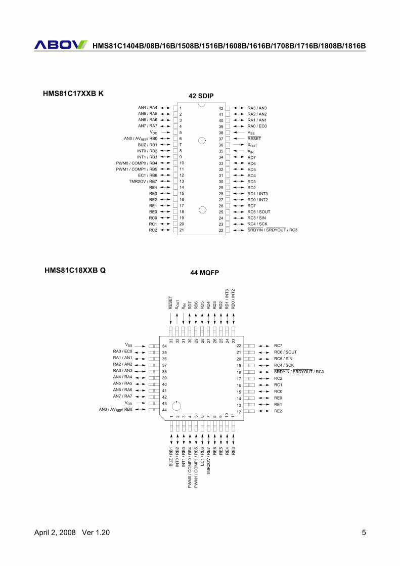
42 SDIPHMS81C17XXB K
RE4TMR2OV / RB7
AN5 / RA5AN6 / RA6AN7 / RA7
VDD
AN0 / AVREF/ RB0BUZ / RB1INT0 / RB2INT1 / RB3
PWM0 / COMP0 / RB4PWM1 / COMP1 / RB5
EC1 / RB6
AN4 / RA4
RD2RD3
RA2 / AN2RA1 / AN1RA0 / EC0VSS
RESETXOUT
XIN
RD7RD6RD5RD4
RA3 / AN3
RE2RE3
RD0 / INT2RD1 / INT3
RE0RE1
RC6 / SOUTRC7
RC1RC0
RC4 / SCKRC5 / SIN
RC2 SRDYIN / SRDYOUT / RC3
234567891011121314
1
15161718192021
41403938373635343332313029
42
28272625242322
44 MQFPHMS81C18XXB Q
3435363738394041424344
2221201918171615141312
33 32 31 30 29 28 27 26 25 24 23
1 2 3 4 5 6 7 8 9 10 11
RE6
TMR
2OV
/ RB7
BU
Z / R
B1IN
T0 /
RB2
INT1
/ R
B3PW
M0
/ CO
MP
0 / R
B4PW
M1
/ CO
MP
1 / R
B5E
C1
/ RB6
RE5
RE4
RE3
VSS
RA0 / EC0RA1 / AN1RA2 / AN2RA3 / AN3
AN5 / RA5AN6 / RA6AN7 / RA7
AN4 / RA4
VDD
AN0 / AVREF/ RB0
RC6 / SOUT
RC4 / SCKRC5 / SIN
SRDYIN / SRDYOUT / RC3
RC7
RC2RC1RC0RE0RE1RE2
RD
2R
D3
RE
SET
XO
UT
XIN
RD
7R
D6
RD
5R
D4
RD
0 / I
NT2
RD
1 / I
NT3
April 2, 2008 Ver 1.20 5
HMS81C1404B/08B/16B/1508B/1516B/1608B/1616B/1708B/1716B/1808B/1816B
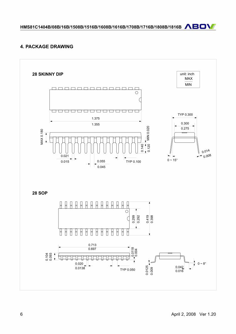
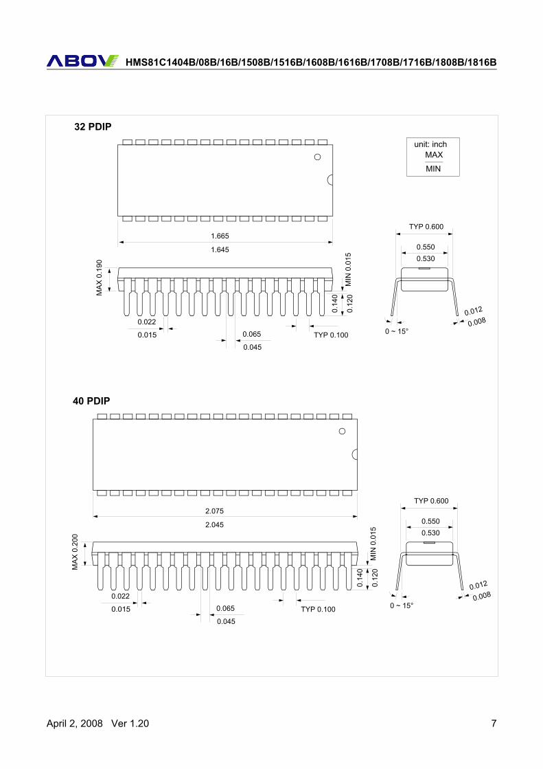
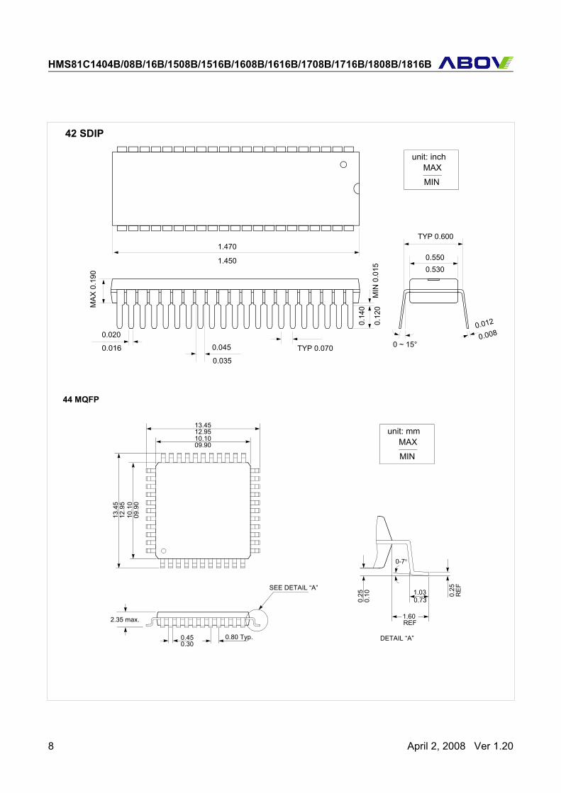
4. PACKAGE DRAWING
1.375
0.015
0.045TYP 0.100
TYP 0.300
0.300
0.014
0 ~ 15°
MAX
0.1
80
MIN
0.0
200.
120
0.29
2
0.39
8
0.713
0.10
4
0.0138 TYP 0.050
0.00
4
0.00
9
0 ~ 8°
0.016
28 SKINNY DIP
28 SOP
unit: inchMAX
MIN
1.355
0.021
0.14
0
0.0550.008
0.275
0.41
9
0.29
9
0.697
0.09
3
0.0200.042
0.01
25
0.01
18
6 April 2, 2008 Ver 1.20
HMS81C1404B/08B/16B/1508B/1516B/1608B/1616B/1708B/1716B/1808B/1816B
1.665
0.015
0.045TYP 0.100
TYP 0.600
0.550
0.012
0 ~ 15°
MA
X 0
.190
MIN
0.0
150.
120
32 PDIPunit: inch
MAX
MIN
1.645
0.022
0.14
00.065
0.008
0.530
2.075
0.015
0.045TYP 0.100
TYP 0.600
0.550
0.012
0 ~ 15°
MA
X 0
.200
MIN
0.0
150.
120
40 PDIP
2.045
0.022
0.14
0
0.0650.008
0.530
April 2, 2008 Ver 1.20 7
HMS81C1404B/08B/16B/1508B/1516B/1608B/1616B/1708B/1716B/1808B/1816B
1.470
0.016
0.035TYP 0.070
TYP 0.600
0.550
0.012
0 ~ 15°
MA
X 0
.190
MIN
0.0
150.
120
42 SDIP
1.450
0.020
0.14
0
0.0450.008
0.530
10.1009.90
13.4512.95
13.4
512
.95
10.1
009
.90
2.35 max.
0.450.30
0.80 Typ.
SEE DETAIL “A”1.030.73
0-7°
0.25
0.10 0.
25R
EF
1.60REF
DETAIL “A”
44 MQFP
unit: inchMAX
MIN
unit: mmMAX
MIN
8 April 2, 2008 Ver 1.20
HMS81C1404B/08B/16B/1508B/1516B/1608B/1616B/1708B/1716B/1808B/1816B
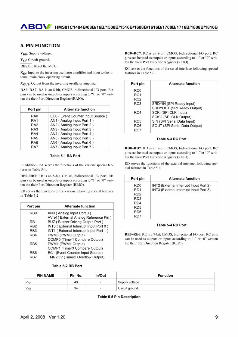
5. PIN FUNCTIONVDD: Supply voltage.
VSS: Circuit ground.
RESET: Reset the MCU.
XIN: Input to the inverting oscillator amplifier and input to the in-ternal main clock operating circuit.
XOUT: Output from the inverting oscillator amplifier.
RA0~RA7: RA is an 8-bit, CMOS, bidirectional I/O port. RApins can be used as outputs or inputs according to “1” or “0” writ-ten the their Port Direction Register(RAIO).
In addition, RA serves the functions of the various special fea-tures in Table 5-1.
RB0~RB7: RB is an 8-bit, CMOS, bidirectional I/O port. RBpins can be used as outputs or inputs according to “1” or “0” writ-ten the their Port Direction Register (RBIO).
RB serves the functions of the various following special featuresin Table 5-2
RC0~RC7: RC is an 8-bit, CMOS, bidirectional I/O port. RCpins can be used as outputs or inputs according to “1” or “0” writ-ten the their Port Direction Register (RCIO).
RC serves the functions of the serial interface following specialfeatures in Table 5-3.
RD0~RD7: RD is an 8-bit, CMOS, bidirectional I/O port. RCpins can be used as outputs or inputs according to “1” or “0” writ-ten the their Port Direction Register (RDIO).
RD serves the functions of the external interrupt following spe-cial features in Table 5-4
RE0~RE6: RE is a 7-bit, CMOS, bidirectional I/O port. RC pinscan be used as outputs or inputs according to “1” or “0” writtenthe their Port Direction Register (REIO).
Port pin Alternate function
RA0RA1RA2RA3RA4RA5RA6RA7
EC0 ( Event Counter Input Source )AN1 ( Analog Input Port 1 )AN2 ( Analog Input Port 2 )AN3 ( Analog Input Port 3 )AN4 ( Analog Input Port 4 )AN5 ( Analog Input Port 5 )AN6 ( Analog Input Port 6 )AN7 ( Analog Input Port 7 )
Table 5-1 RA Port
Port pin Alternate function
RB0
RB1RB2RB3RB4
RB5
RB6RB7
AN0 ( Analog Input Port 0 )AVref ( External Analog Reference Pin )BUZ ( Buzzer Driving Output Port )INT0 ( External Interrupt Input Port 0 )INT1 ( External Interrupt Input Port 1 )PWM0 (PWM0 Output)COMP0 (Timer1 Compare Output)PWM1 (PWM1 Output)COMP1 (Timer3 Compare Output)EC1 (Event Counter Input Source)TMR2OV (Timer2 Overflow Output)
Table 5-2 RB Port
Port pin Alternate function
RC0RC1RC2RC3
RC4
RC5RC6RC7
SRDYIN (SPI Ready Input)SRDYOUT (SPI Ready Output)SCKI (SPI CLK Input)SCKO (SPI CLK Output)SIN (SPI Serial Data Input)SOUT (SPI Serial Data Output)
Table 5-3 RC Port
Port pin Alternate function
RD0RD1RD2RD3RD4RD5RD6RD7
INT2 (External Interrupt Input Port 2)INT3 (External Interrupt Input Port 3)
Table 5-4 RD Port
PIN NAME Pin No. In/Out Function
VDD 43 - Supply voltage
VSS 34 - Circuit ground
Table 5-5 Pin Description
April 2, 2008 Ver 1.20 9
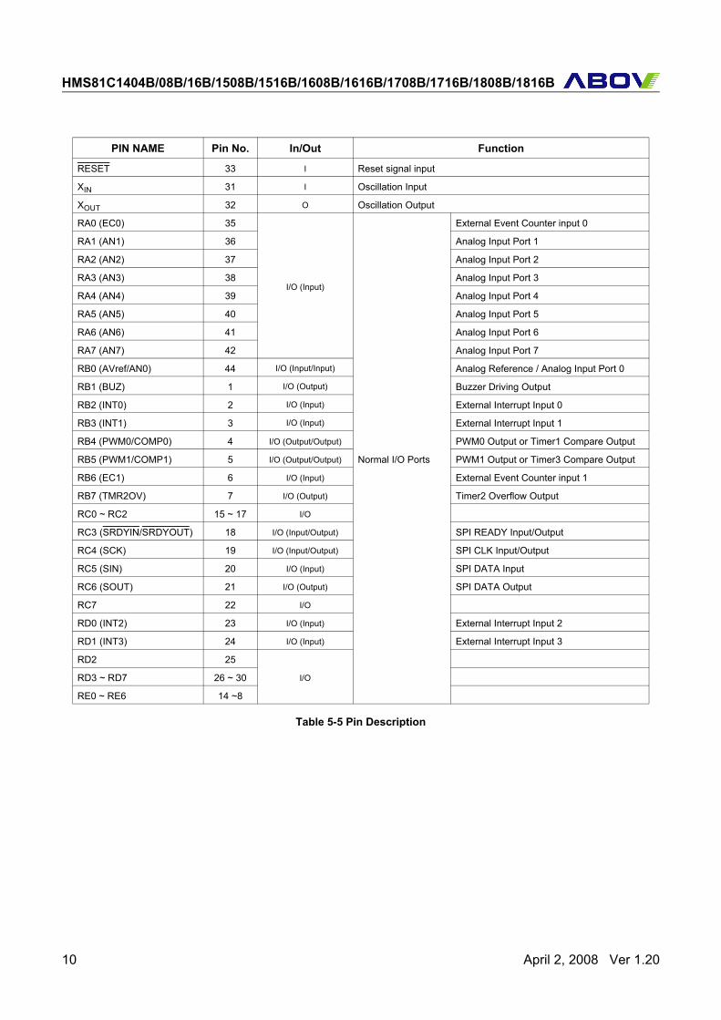
HMS81C1404B/08B/16B/1508B/1516B/1608B/1616B/1708B/1716B/1808B/1816B
RESET 33 I Reset signal input
XIN 31 I Oscillation Input
XOUT 32 O Oscillation Output
RA0 (EC0) 35
I/O (Input)
Normal I/O Ports
External Event Counter input 0
RA1 (AN1) 36 Analog Input Port 1
RA2 (AN2) 37 Analog Input Port 2
RA3 (AN3) 38 Analog Input Port 3
RA4 (AN4) 39 Analog Input Port 4
RA5 (AN5) 40 Analog Input Port 5
RA6 (AN6) 41 Analog Input Port 6
RA7 (AN7) 42 Analog Input Port 7
RB0 (AVref/AN0) 44 I/O (Input/Input) Analog Reference / Analog Input Port 0
RB1 (BUZ) 1 I/O (Output) Buzzer Driving Output
RB2 (INT0) 2 I/O (Input) External Interrupt Input 0
RB3 (INT1) 3 I/O (Input) External Interrupt Input 1
RB4 (PWM0/COMP0) 4 I/O (Output/Output) PWM0 Output or Timer1 Compare Output
RB5 (PWM1/COMP1) 5 I/O (Output/Output) PWM1 Output or Timer3 Compare Output
RB6 (EC1) 6 I/O (Input) External Event Counter input 1
RB7 (TMR2OV) 7 I/O (Output) Timer2 Overflow Output
RC0 ~ RC2 15 ~ 17 I/O
RC3 (SRDYIN/SRDYOUT) 18 I/O (Input/Output) SPI READY Input/Output
RC4 (SCK) 19 I/O (Input/Output) SPI CLK Input/Output
RC5 (SIN) 20 I/O (Input) SPI DATA Input
RC6 (SOUT) 21 I/O (Output) SPI DATA Output
RC7 22 I/O
RD0 (INT2) 23 I/O (Input) External Interrupt Input 2
RD1 (INT3) 24 I/O (Input) External Interrupt Input 3
RD2 25
I/ORD3 ~ RD7 26 ~ 30
RE0 ~ RE6 14 ~8
PIN NAME Pin No. In/Out Function
Table 5-5 Pin Description
10 April 2, 2008 Ver 1.20
HMS81C1404B/08B/16B/1508B/1516B/1608B/1616B/1708B/1716B/1808B/1816B
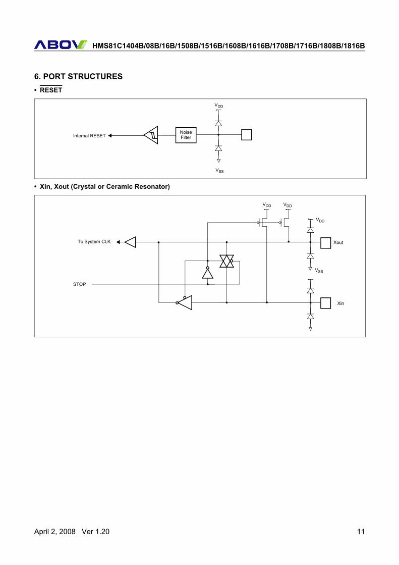
6. PORT STRUCTURES• RESET
• Xin, Xout (Crystal or Ceramic Resonator)
VSS
Internal RESET
VDD
NoiseFilter
VSS
Xout
Xin
STOP
To System CLK
VDD
VDDVDD
April 2, 2008 Ver 1.20 11
HMS81C1404B/08B/16B/1508B/1516B/1608B/1616B/1708B/1716B/1808B/1816B
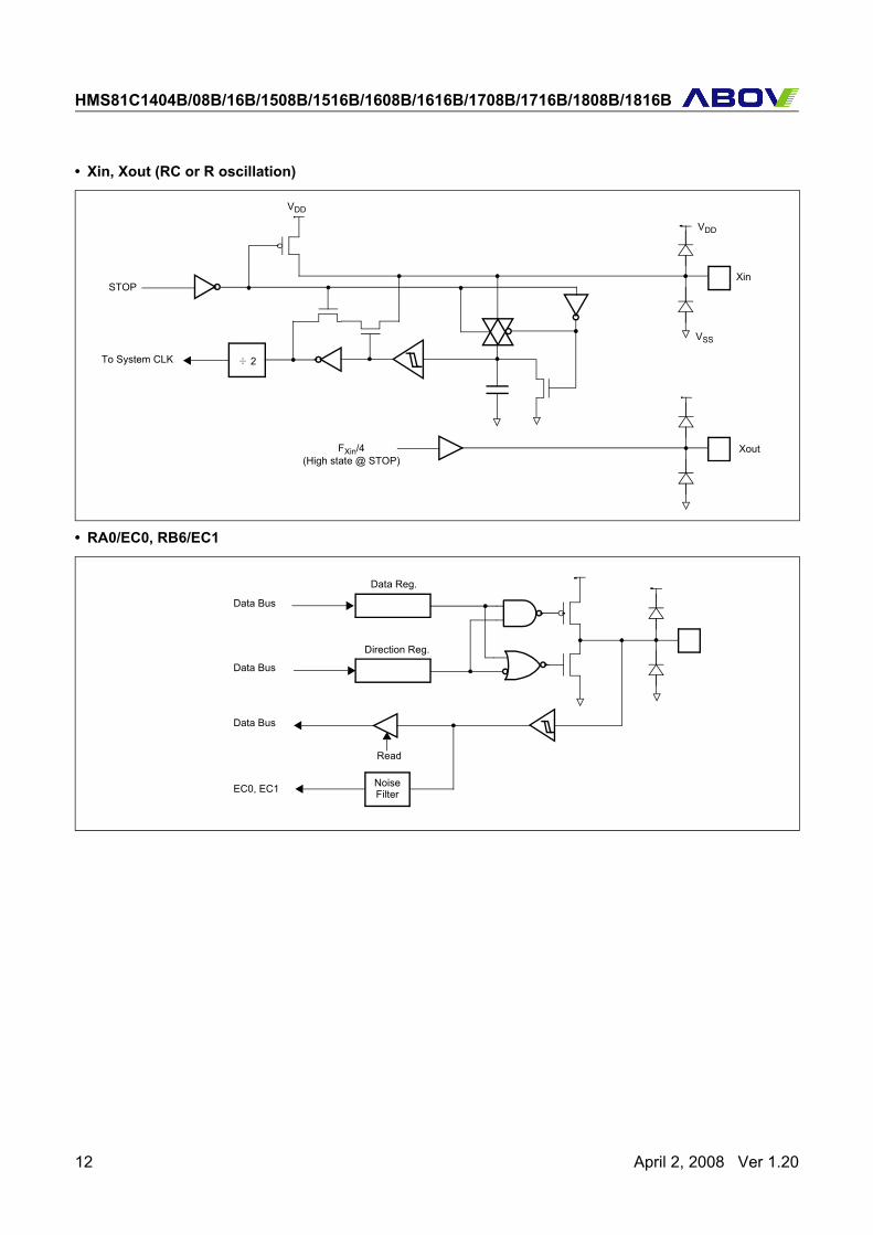
• Xin, Xout (RC or R oscillation)
• RA0/EC0, RB6/EC1
VSS
Xin
Xout
STOP
VDD
VDD
FXin/4(High state @ STOP)
÷ 2To System CLK
Data Bus
Data Bus
Data Bus
Data Reg.
Direction Reg.
Read
EC0, EC1 NoiseFilter
12 April 2, 2008 Ver 1.20
HMS81C1404B/08B/16B/1508B/1516B/1608B/1616B/1708B/1716B/1808B/1816B
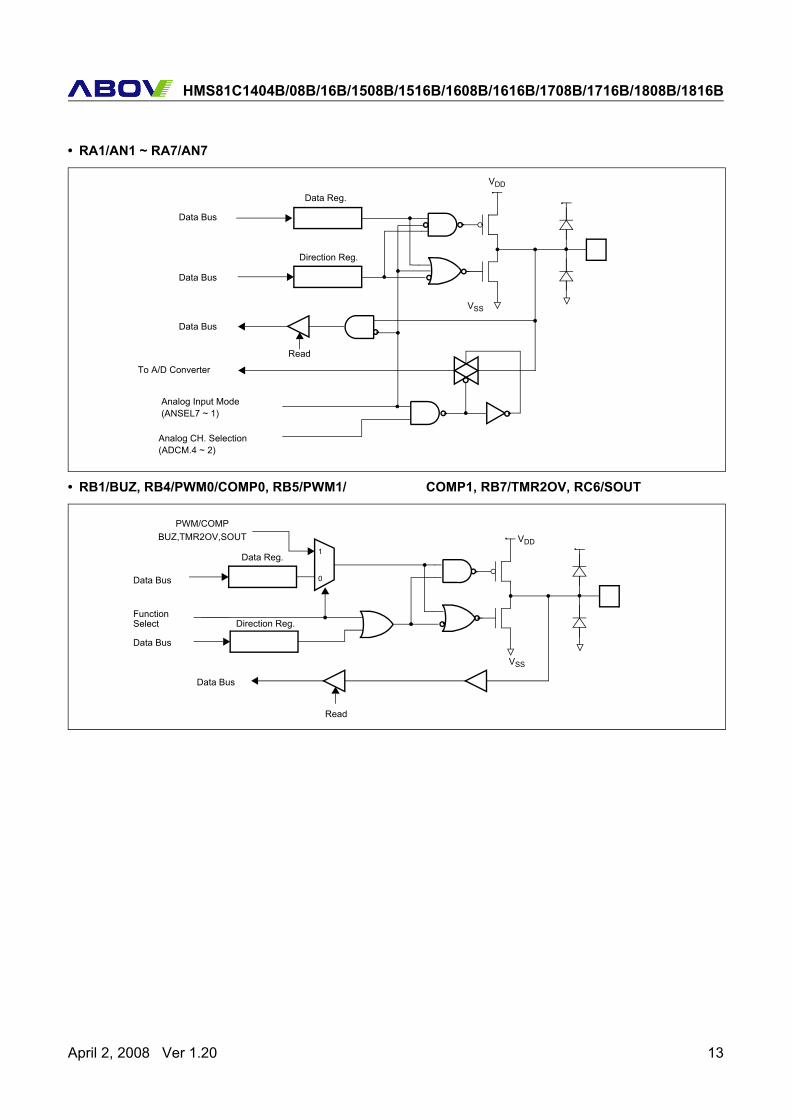
• RA1/AN1 ~ RA7/AN7
• RB1/BUZ, RB4/PWM0/COMP0, RB5/PWM1/ COMP1, RB7/TMR2OV, RC6/SOUT
VDD
VSS
Data Bus
Data Bus
Data Bus
Read
To A/D Converter
Analog Input Mode(ANSEL7 ~ 1)
Analog CH. Selection(ADCM.4 ~ 2)
Data Reg.
Direction Reg.
VDD
VSS
Data Bus
Data Bus
Data Bus
Read
0
1
FunctionSelect
PWM/COMPBUZ,TMR2OV,SOUT
Data Reg.
Direction Reg.
April 2, 2008 Ver 1.20 13
HMS81C1404B/08B/16B/1508B/1516B/1608B/1616B/1708B/1716B/1808B/1816B
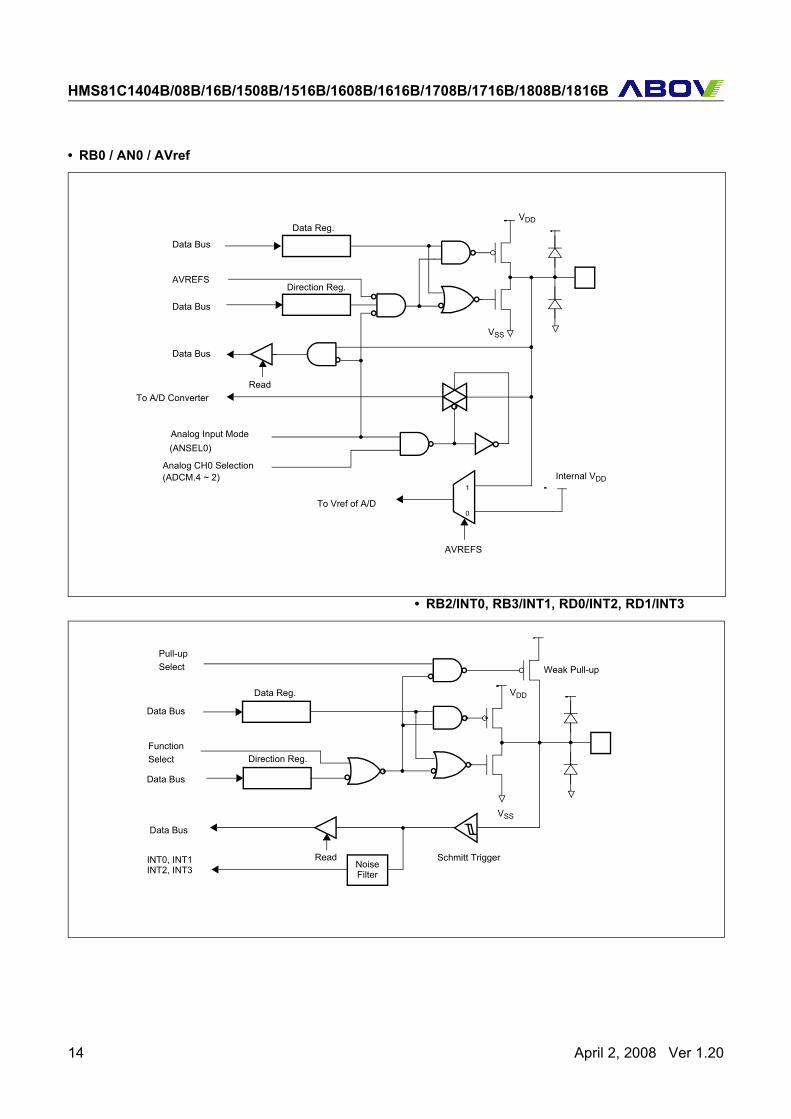
• RB0 / AN0 / AVref
• RB2/INT0, RB3/INT1, RD0/INT2, RD1/INT3
VDD
VSS
Data Bus
Data Bus
Data Bus
ReadTo A/D Converter
Analog Input Mode(ANSEL0)
Analog CH0 Selection(ADCM.4 ~ 2)
AVREFS
AVREFS
Internal VDD
0
1
To Vref of A/D
Data Reg.
Direction Reg.
VDD
VSS
Data Bus
Data Bus
Data Bus
Read
FunctionSelect
Pull-upSelect
INT0, INT1 Schmitt Trigger
Weak Pull-up
Data Reg.
Direction Reg.
INT2, INT3 NoiseFilter
14 April 2, 2008 Ver 1.20
HMS81C1404B/08B/16B/1508B/1516B/1608B/1616B/1708B/1716B/1808B/1816B
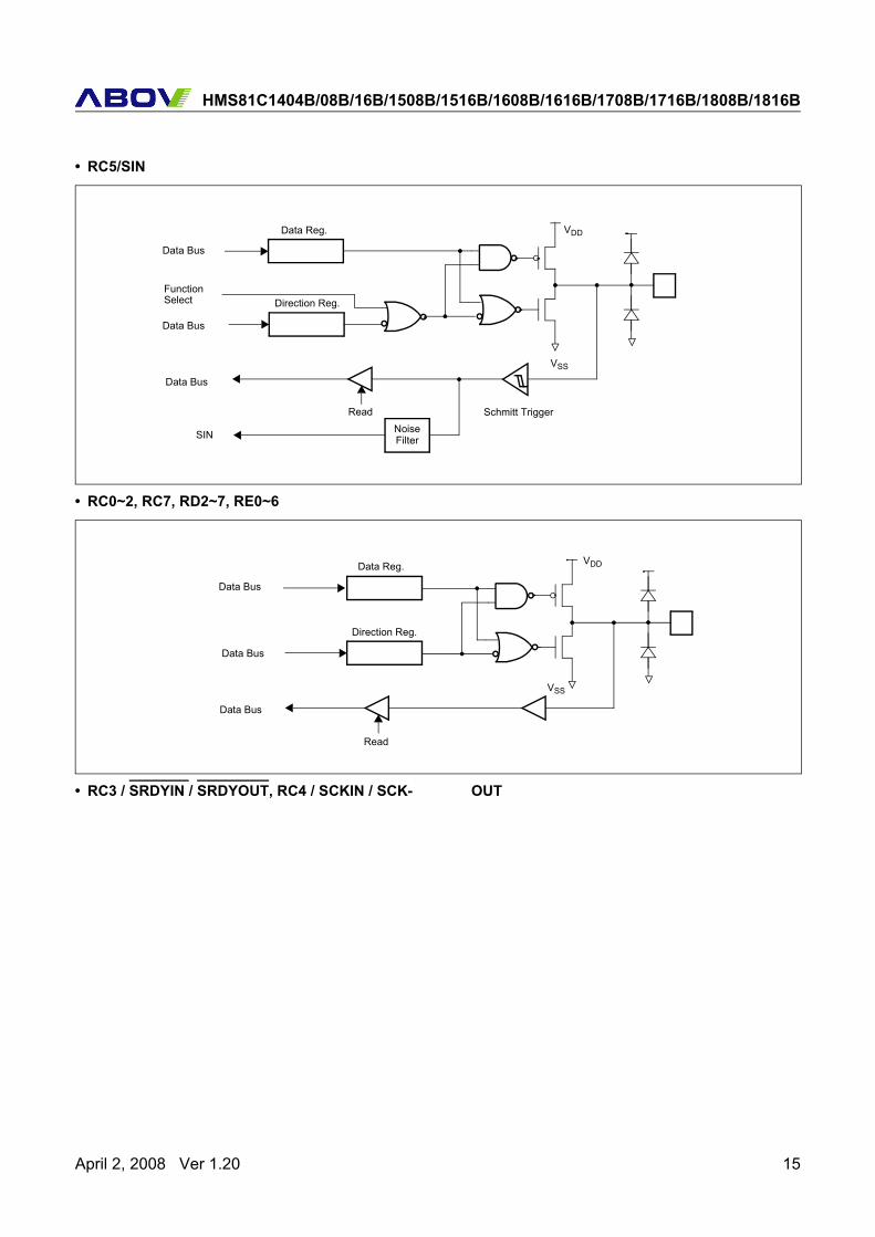
• RC5/SIN
• RC0~2, RC7, RD2~7, RE0~6
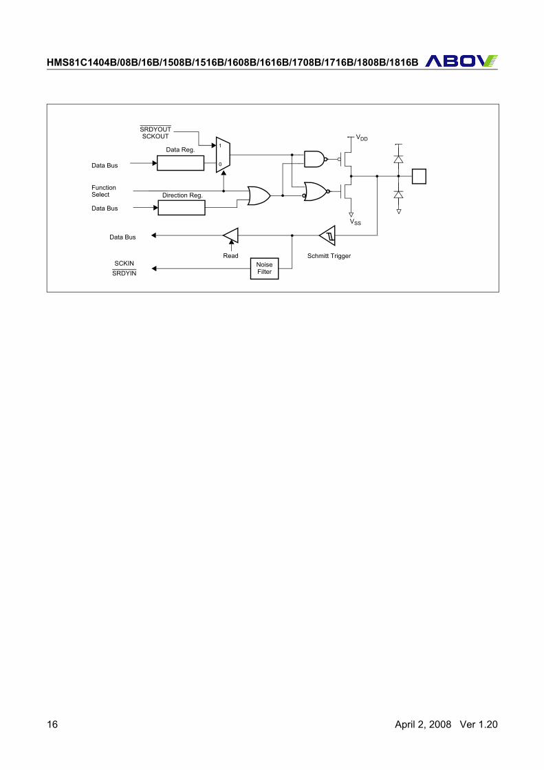
• RC3 / SRDYIN / SRDYOUT, RC4 / SCKIN / SCK- OUT
VDD
VSS
Data Bus
Data Bus
Data Bus
Read
FunctionSelect
Schmitt Trigger
Data Reg.
Direction Reg.
SIN NoiseFilter
VDD
VSS
Data Bus
Data Bus
Data Bus
Read
Data Reg.
Direction Reg.
April 2, 2008 Ver 1.20 15
HMS81C1404B/08B/16B/1508B/1516B/1608B/1616B/1708B/1716B/1808B/1816B
VDD
VSS
Data Bus
Data Bus
0
1
FunctionSelect
SRDYOUTSCKOUT
Data Reg.
Direction Reg.
Data Bus
Read Schmitt TriggerSCKIN
SRDYINNoiseFilter
16 April 2, 2008 Ver 1.20
HMS81C1404B/08B/16B/1508B/1516B/1608B/1616B/1708B/1716B/1808B/1816B
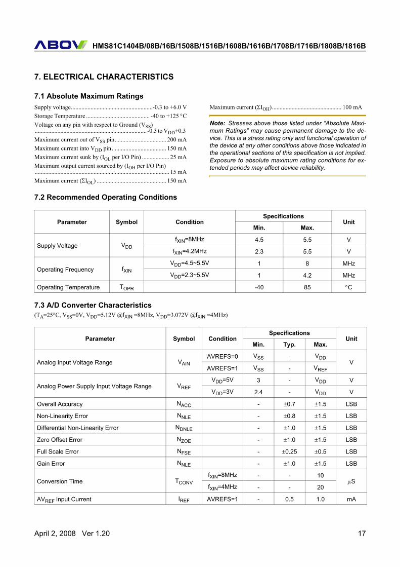
7. ELECTRICAL CHARACTERISTICS
7.1 Absolute Maximum RatingsSupply voltage......................................................-0.3 to +6.0 VStorage Temperature .......................................... -40 to +125 °CVoltage on any pin with respect to Ground (VSS).......................................................................... -0.3 to VDD+0.3 Maximum current out of VSS pin.................................. 200 mAMaximum current into VDD pin .................................... 150 mAMaximum current sunk by (IOL per I/O Pin) .................. 25 mAMaximum output current sourced by (IOH per I/O Pin)......................................................................................... 15 mAMaximum current (ΣIOL) .............................................. 150 mA
Maximum current (ΣIOH).............................................. 100 mA
Note: Stresses above those listed under “Absolute Maxi-mum Ratings” may cause permanent damage to the de-vice. This is a stress rating only and functional operation ofthe device at any other conditions above those indicated inthe operational sections of this specification is not implied.Exposure to absolute maximum rating conditions for ex-tended periods may affect device reliability.
7.2 Recommended Operating Conditions
7.3 A/D Converter Characteristics(TA=25°C, VSS=0V, VDD=5.12V @fXIN =8MHz, VDD=3.072V @fXIN =4MHz)
Parameter Symbol ConditionSpecifications
UnitMin. Max.
Supply Voltage VDDfXIN=8MHz 4.5 5.5 V
fXIN=4.2MHz 2.3 5.5 V
Operating Frequency fXINVDD=4.5~5.5V 1 8 MHz
VDD=2.3~5.5V 1 4.2 MHz
Operating Temperature TOPR -40 85 °C
Parameter Symbol ConditionSpecifications
UnitMin. Typ. Max.
Analog Input Voltage Range VAINAVREFS=0 VSS - VDD
VAVREFS=1 VSS - VREF
Analog Power Supply Input Voltage Range VREFVDD=5V 3 - VDD V
VDD=3V 2.4 - VDD V
Overall Accuracy NACC - ±0.7 ±1.5 LSB
Non-Linearity Error NNLE - ±0.8 ±1.5 LSB
Differential Non-Linearity Error NDNLE - ±1.0 ±1.5 LSB
Zero Offset Error NZOE - ±1.0 ±1.5 LSB
Full Scale Error NFSE - ±0.25 ±0.5 LSB
Gain Error NNLE - ±1.0 ±1.5 LSB
Conversion Time TCONVfXIN=8MHz - - 10
μSfXIN=4MHz - - 20
AVREF Input Current IREF AVREFS=1 - 0.5 1.0 mA
April 2, 2008 Ver 1.20 17
HMS81C1404B/08B/16B/1508B/1516B/1608B/1616B/1708B/1716B/1808B/1816B
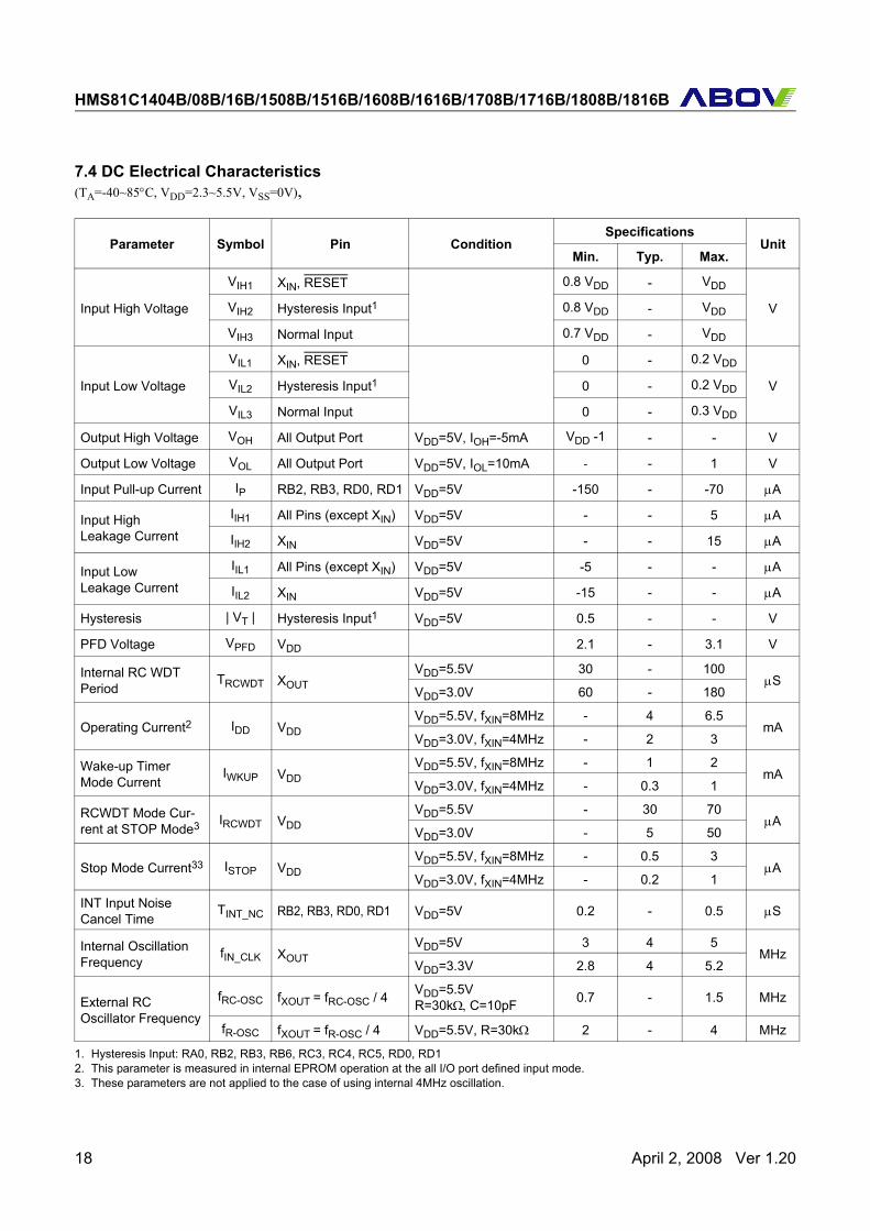
7.4 DC Electrical Characteristics(TA=-40~85°C, VDD=2.3~5.5V, VSS=0V),
Parameter Symbol Pin ConditionSpecifications
UnitMin. Typ. Max.
Input High Voltage
VIH1 XIN, RESET 0.8 VDD - VDD
VVIH2 Hysteresis Input1 0.8 VDD - VDD
VIH3 Normal Input 0.7 VDD - VDD
Input Low Voltage
VIL1 XIN, RESET 0 - 0.2 VDD
VVIL2 Hysteresis Input1 0 - 0.2 VDD
VIL3 Normal Input 0 - 0.3 VDD
Output High Voltage VOH All Output Port VDD=5V, IOH=-5mA VDD -1 - - V
Output Low Voltage VOL All Output Port VDD=5V, IOL=10mA - - 1 V
Input Pull-up Current IP RB2, RB3, RD0, RD1 VDD=5V -150 - -70 μA
Input HighLeakage Current
IIH1 All Pins (except XIN) VDD=5V - - 5 μA
IIH2 XIN VDD=5V - - 15 μA
Input LowLeakage Current
IIL1 All Pins (except XIN) VDD=5V -5 - - μA
IIL2 XIN VDD=5V -15 - - μA
Hysteresis | VT | Hysteresis Input1 VDD=5V 0.5 - - V
PFD Voltage VPFD VDD 2.1 - 3.1 V
Internal RC WDT Period
TRCWDT XOUTVDD=5.5V 30 - 100
μSVDD=3.0V 60 - 180
Operating Current2 IDD VDDVDD=5.5V, fXIN=8MHz - 4 6.5
mAVDD=3.0V, fXIN=4MHz - 2 3
Wake-up Timer Mode Current
IWKUP VDDVDD=5.5V, fXIN=8MHz - 1 2
mAVDD=3.0V, fXIN=4MHz - 0.3 1
RCWDT Mode Cur-rent at STOP Mode3 IRCWDT VDD
VDD=5.5V - 30 70μA
VDD=3.0V - 5 50
Stop Mode Current33 ISTOP VDDVDD=5.5V, fXIN=8MHz - 0.5 3
μAVDD=3.0V, fXIN=4MHz - 0.2 1
INT Input Noise Cancel Time
TINT_NC RB2, RB3, RD0, RD1 VDD=5V 0.2 - 0.5 μS
Internal Oscillation Frequency
fIN_CLK XOUTVDD=5V 3 4 5
MHzVDD=3.3V 2.8 4 5.2
External RC Oscillator Frequency
fRC-OSC fXOUT = fRC-OSC / 4 VDD=5.5VR=30kΩ, C=10pF 0.7 - 1.5 MHz
fR-OSC fXOUT = fR-OSC / 4 VDD=5.5V, R=30kΩ 2 - 4 MHz
1. Hysteresis Input: RA0, RB2, RB3, RB6, RC3, RC4, RC5, RD0, RD12. This parameter is measured in internal EPROM operation at the all I/O port defined input mode.3. These parameters are not applied to the case of using internal 4MHz oscillation.
18 April 2, 2008 Ver 1.20
HMS81C1404B/08B/16B/1508B/1516B/1608B/1616B/1708B/1716B/1808B/1816B
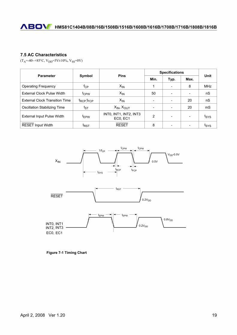
7.5 AC Characteristics(TA=-40~+85°C, VDD=5V±10%, VSS=0V)
Figure 7-1 Timing Chart
Parameter Symbol PinsSpecifications
UnitMin. Typ. Max.
Operating Frequency fCP XIN 1 - 8 MHz
External Clock Pulse Width tCPW XIN 50 - - nS
External Clock Transition Time tRCP,tFCP XIN - - 20 nS
Oscillation Stabilizing Time tST XIN, XOUT - - 20 mS
External Input Pulse Width tEPWINT0, INT1, INT2, INT3
EC0, EC1 2 - - tSYS
RESET Input Width tRST RESET 8 - - tSYS
tRCP tFCP
XIN
INT0, INT1INT2,
0.5V
VDD-0.5V
0.2VDD
RESET
0.2VDD
0.8VDD
EC0,
tRST
tEPWtEPW
1/fCPtCPW tCPW
tSYS
INT3 EC1
April 2, 2008 Ver 1.20 19
HMS81C1404B/08B/16B/1508B/1516B/1608B/1616B/1708B/1716B/1808B/1816B
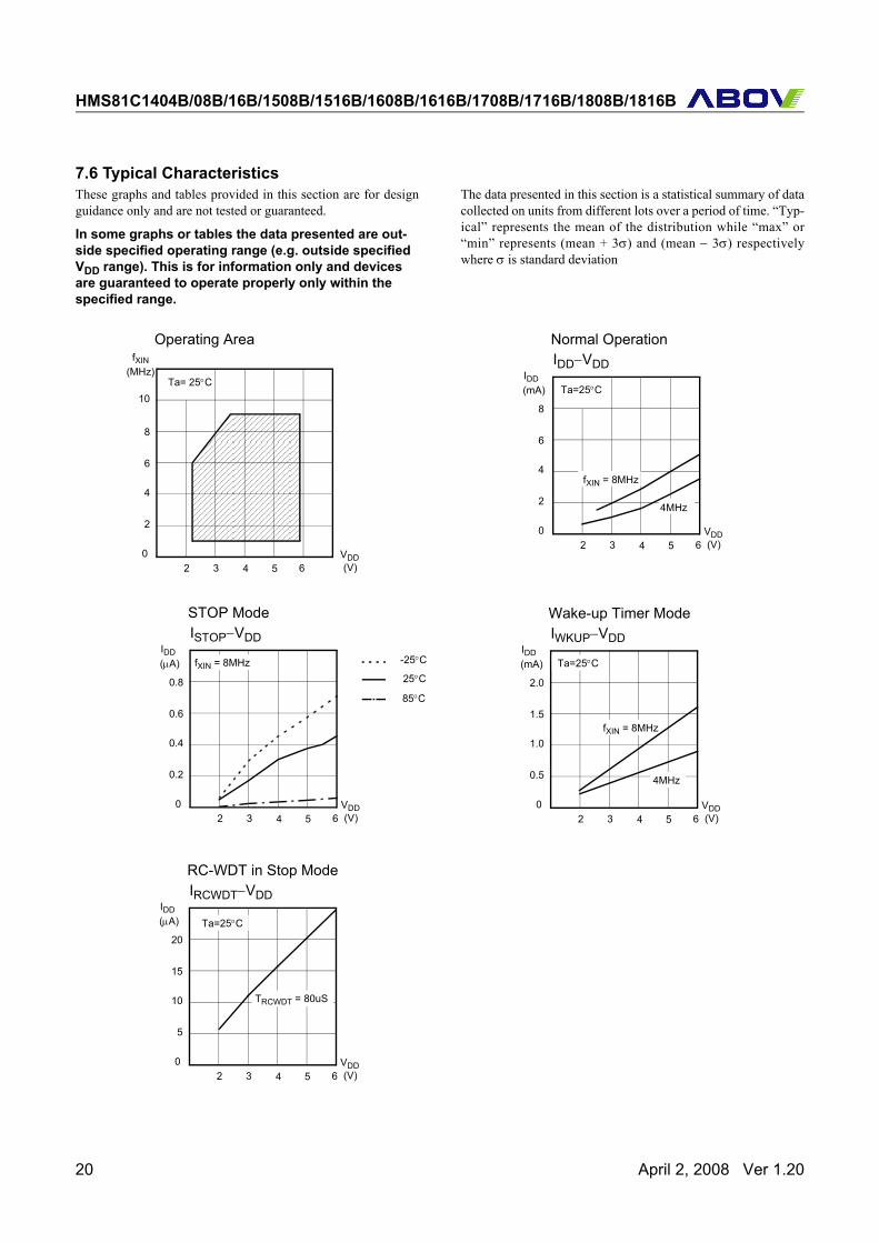
7.6 Typical CharacteristicsThese graphs and tables provided in this section are for designguidance only and are not tested or guaranteed.
In some graphs or tables the data presented are out-side specified operating range (e.g. outside specified VDD range). This is for information only and devices are guaranteed to operate properly only within the specified range.
The data presented in this section is a statistical summary of datacollected on units from different lots over a period of time. “Typ-ical” represents the mean of the distribution while “max” or“min” represents (mean + 3σ) and (mean − 3σ) respectivelywhere σ is standard deviation
Ta= 25°CTa=25°C
IDD−VDD
8
6
4
2
0
(mA)IDD
2 3 4 5 6VDD(V)
Normal Operation
8
6
4
2
0
(MHz)fXIN
2 3 4 5 6VDD(V)
Operating Area
fXIN = 8MHz
4MHz
10
IWKUP−VDD
2.0
1.5
1.0
0.5
0
(mA)IDD
2 3 4 5 6VDD(V)
Wake-up Timer Mode
IRCWDT−VDD
20
15
10
5
0
(μA)IDD
2 3 4 5 6VDD(V)
RC-WDT in Stop Mode
Ta=25°C
fXIN = 8MHz
4MHz
Ta=25°C
ISTOP−VDD
0.8
0.6
0.4
0.2
0
(μA)IDD
2 3 4 5 6VDD(V)
STOP Mode
fXIN = 8MHz -25°C
85°C
25°C
TRCWDT = 80uS
20 April 2, 2008 Ver 1.20
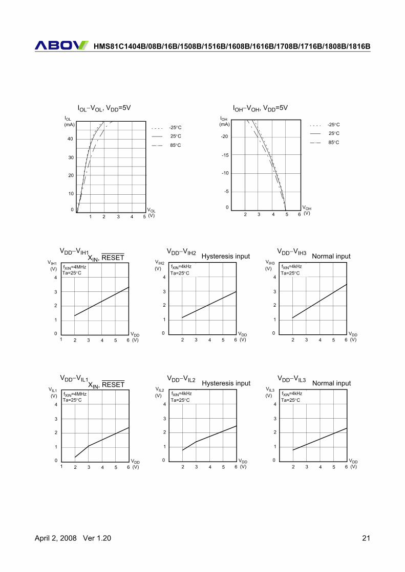
HMS81C1404B/08B/16B/1508B/1516B/1608B/1616B/1708B/1716B/1808B/1816B
IOL−VOL, VDD=5V
40
30
20
10
0
(mA)IOL
VOL(V)
IOH−VOH, VDD=5V
-20
-15
-10
-5
0
(mA)IOH
2 3 4 5 6VOH(V)
1 2 3 4 5
fXIN=4MHz
VDD−VIH1
4
3
2
1
0
(V)VIH1
2 3 4 5 6VDD(V)
VDD−VIH2
4
3
2
1
0
(V)VIH2
2 3 4 5 6VDD(V)
Ta=25°CfXIN=4kHzTa=25°C
1
XIN, RESET Hysteresis input
-25°C
85°C
25°C-25°C
85°C
25°C
VDD−VIH3
4
3
2
1
0
(V)VIH3
2 3 4 5 6VDD(V)
fXIN=4kHzTa=25°C
Normal input
fXIN=4MHz
VDD−VIL1
4
3
2
1
0
(V)VIL1
2 3 4 5 6VDD(V)
VDD−VIL2
4
3
2
1
0
(V)VIL2
2 3 4 5 6VDD(V)
Ta=25°CfXIN=4kHzTa=25°C
1
XIN, RESET Hysteresis inputVDD−VIL3
4
3
2
1
0
(V)VIL3
2 3 4 5 6VDD(V)
fXIN=4kHzTa=25°C
Normal input
April 2, 2008 Ver 1.20 21
HMS81C1404B/08B/16B/1508B/1516B/1608B/1616B/1708B/1716B/1808B/1816B
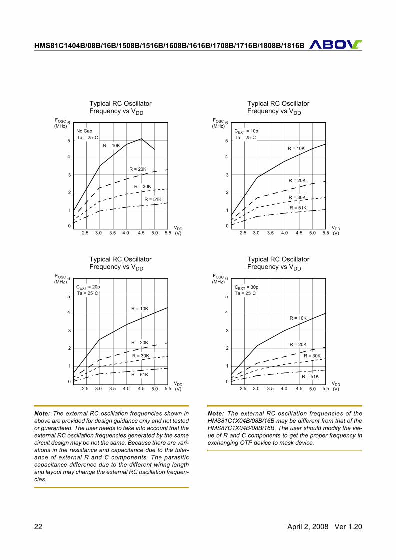
Note: The external RC oscillation frequencies shown inabove are provided for design guidance only and not testedor guaranteed. The user needs to take into account that theexternal RC oscillation frequencies generated by the samecircuit design may be not the same. Because there are vari-ations in the resistance and capacitance due to the toler-ance of external R and C components. The parasiticcapacitance difference due to the different wiring lengthand layout may change the external RC oscillation frequen-cies.
Note: The external RC oscillation frequencies of theHMS81C1X04B/08B/16B may be different from that of theHMS87C1X04B/08B/16B. The user should modify the val-ue of R and C components to get the proper frequency inexchanging OTP device to mask device.
Typical RC Oscillator
4
3
2
1
0
(MHz)FOSC
2.5 3.0 3.5 4.0 4.5VDD(V)
Frequency vs VDD
5
6
5.0 5.5
Ta = 25°CNo Cap
R = 10K
R = 20K
R = 51K
Typical RC Oscillator
4
3
2
1
0
(MHz)FOSC
2.5 3.0 3.5 4.0 4.5VDD(V)
Frequency vs VDD
5
6
5.0 5.5
Ta = 25°C
R = 10K
R = 20K
R = 30K
R = 51K
Typical RC Oscillator
4
3
2
1
0
(MHz)FOSC
2.5 3.0 3.5 4.0 4.5VDD(V)
Frequency vs VDD
5
6
5.0 5.5
Ta = 25°C
R = 10K
R = 20K
R = 30K
R = 51K
Typical RC Oscillator
4
3
2
1
0
(MHz)FOSC
2.5 3.0 3.5 4.0 4.5VDD(V)
Frequency vs VDD
5
6
5.0 5.5
Ta = 25°C
R = 10K
R = 20K
R = 30K
R = 51K
CEXT = 10p
CEXT = 20p CEXT = 30p
R = 30K
22 April 2, 2008 Ver 1.20
HMS81C1404B/08B/16B/1508B/1516B/1608B/1616B/1708B/1716B/1808B/1816B
8. MEMORY ORGANIZATIONThe HMS81C1X04B/08B/16B has separate address spaces forProgram memory and Data Memory. The Program memory canonly be read, not written to. It can be up to 4K /8K /16K bytes of
Program memory. The Data memory can be read and written toup to 448 bytes including the stack area.
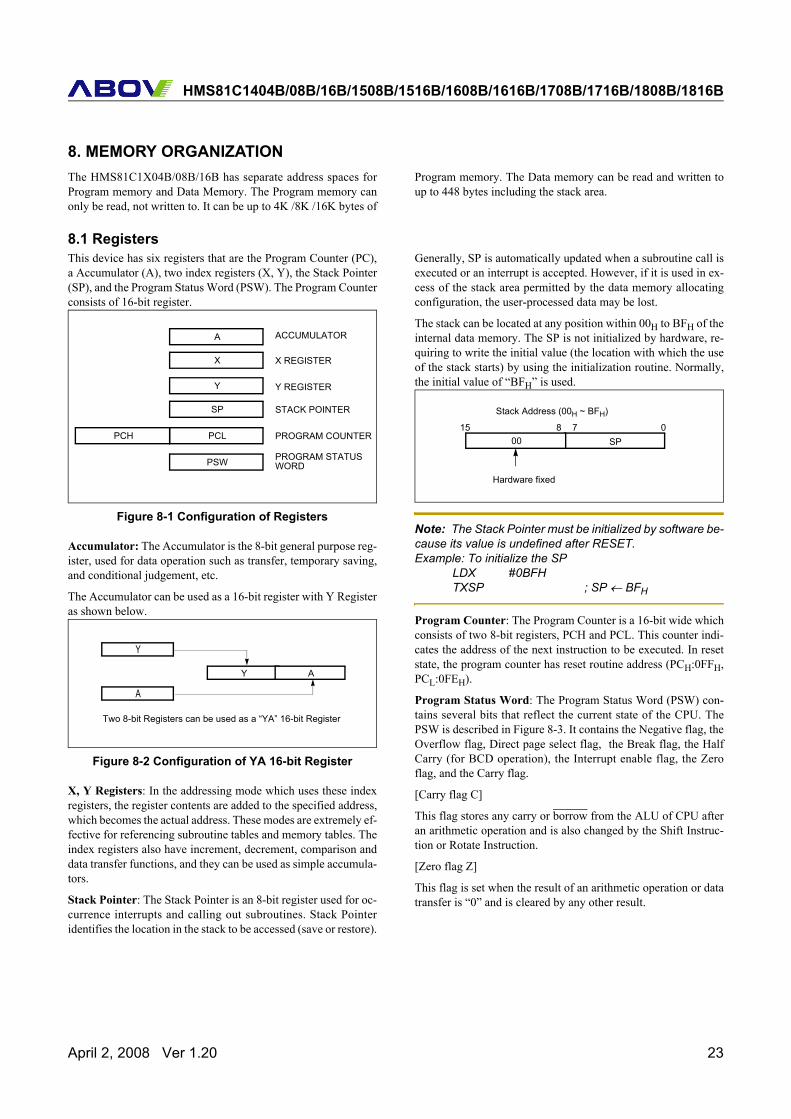
8.1 RegistersThis device has six registers that are the Program Counter (PC),a Accumulator (A), two index registers (X, Y), the Stack Pointer(SP), and the Program Status Word (PSW). The Program Counterconsists of 16-bit register.
Figure 8-1 Configuration of Registers
Accumulator: The Accumulator is the 8-bit general purpose reg-ister, used for data operation such as transfer, temporary saving,and conditional judgement, etc.
The Accumulator can be used as a 16-bit register with Y Registeras shown below.
Figure 8-2 Configuration of YA 16-bit Register
X, Y Registers: In the addressing mode which uses these indexregisters, the register contents are added to the specified address,which becomes the actual address. These modes are extremely ef-fective for referencing subroutine tables and memory tables. Theindex registers also have increment, decrement, comparison anddata transfer functions, and they can be used as simple accumula-tors.
Stack Pointer: The Stack Pointer is an 8-bit register used for oc-currence interrupts and calling out subroutines. Stack Pointeridentifies the location in the stack to be accessed (save or restore).
Generally, SP is automatically updated when a subroutine call isexecuted or an interrupt is accepted. However, if it is used in ex-cess of the stack area permitted by the data memory allocatingconfiguration, the user-processed data may be lost.
The stack can be located at any position within 00H to BFH of theinternal data memory. The SP is not initialized by hardware, re-quiring to write the initial value (the location with which the useof the stack starts) by using the initialization routine. Normally,the initial value of “BFH” is used.
Note: The Stack Pointer must be initialized by software be-cause its value is undefined after RESET.Example: To initialize the SP
LDX #0BFHTXSP ; SP ← BFH
Program Counter: The Program Counter is a 16-bit wide whichconsists of two 8-bit registers, PCH and PCL. This counter indi-cates the address of the next instruction to be executed. In resetstate, the program counter has reset routine address (PCH:0FFH,PCL:0FEH).
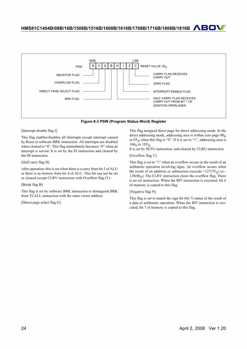
Program Status Word: The Program Status Word (PSW) con-tains several bits that reflect the current state of the CPU. ThePSW is described in Figure 8-3. It contains the Negative flag, theOverflow flag, Direct page select flag, the Break flag, the HalfCarry (for BCD operation), the Interrupt enable flag, the Zeroflag, and the Carry flag.
[Carry flag C]
This flag stores any carry or borrow from the ALU of CPU afteran arithmetic operation and is also changed by the Shift Instruc-tion or Rotate Instruction.
[Zero flag Z]
This flag is set when the result of an arithmetic operation or datatransfer is “0” and is cleared by any other result.
A ACCUMULATOR
X REGISTER
Y REGISTER
STACK POINTER
PROGRAM COUNTER
PROGRAM STATUSWORD
X
Y
SP
PCLPCH
PSW
Two 8-bit Registers can be used as a “YA” 16-bit Register
Y
A
Y A
SP00
Stack Address (00H ~ BFH)
15 08 7
Hardware fixed
April 2, 2008 Ver 1.20 23
HMS81C1404B/08B/16B/1508B/1516B/1608B/1616B/1708B/1716B/1808B/1816B
Figure 8-3 PSW (Program Status Word) Register
[Interrupt disable flag I]
This flag enables/disables all interrupts except interrupt causedby Reset or software BRK instruction. All interrupts are disabledwhen cleared to “0”. This flag immediately becomes “0” when aninterrupt is served. It is set by the EI instruction and cleared bythe DI instruction.
[Half carry flag H]
After operation, this is set when there is a carry from bit 3 of ALUor there is no borrow from bit 4 of ALU. This bit can not be setor cleared except CLRV instruction with Overflow flag (V).
[Break flag B]
This flag is set by software BRK instruction to distinguish BRKfrom TCALL instruction with the same vector address.
[Direct page select flag G]
This flag assigned direct page for direct addressing mode. In thedirect addressing mode, addressing area is within zero page 00Hto FFH when this flag is “0”. If it is set to “1”, addressing area is100H to 1FFH. It is set by SETG instruction, and cleared by CLRG instruction.
[Overflow flag V]
This flag is set to “1” when an overflow occurs as the result of anarithmetic operation involving signs. An overflow occurs whenthe result of an addition or subtraction exceeds +127(7FH) or -128(80H). The CLRV instruction clears the overflow flag. Thereis no set instruction. When the BIT instruction is executed, bit 6of memory is copied to this flag.
[Negative flag N]
This flag is set to match the sign bit (bit 7) status of the result ofa data or arithmetic operation. When the BIT instruction is exe-cuted, bit 7 of memory is copied to this flag.
N
NEGATIVE FLAG
V G B H I Z CMSB LSB
RESET VALUE: 00HPSW
OVERFLOW FLAG
BRK FLAG
CARRY FLAG RECEIVES
ZERO FLAG
INTERRUPT ENABLE FLAG
CARRY OUT
HALF CARRY FLAG RECEIVESCARRY OUT FROM BIT 1 OFADDITION OPERLANDS
DIRECT PAGE SELECT FLAG
24 April 2, 2008 Ver 1.20
HMS81C1404B/08B/16B/1508B/1516B/1608B/1616B/1708B/1716B/1808B/1816B
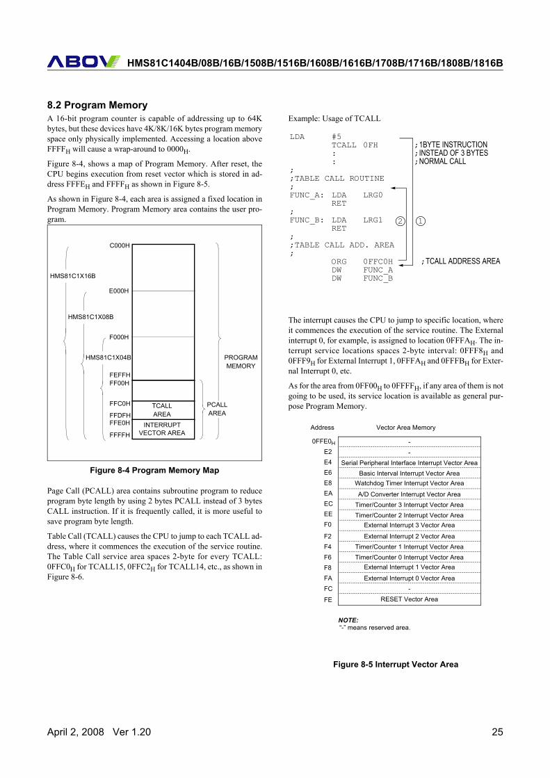
8.2 Program MemoryA 16-bit program counter is capable of addressing up to 64Kbytes, but these devices have 4K/8K/16K bytes program memoryspace only physically implemented. Accessing a location aboveFFFFH will cause a wrap-around to 0000H.
Figure 8-4, shows a map of Program Memory. After reset, theCPU begins execution from reset vector which is stored in ad-dress FFFEH and FFFFH as shown in Figure 8-5.
As shown in Figure 8-4, each area is assigned a fixed location inProgram Memory. Program Memory area contains the user pro-gram.
Figure 8-4 Program Memory Map
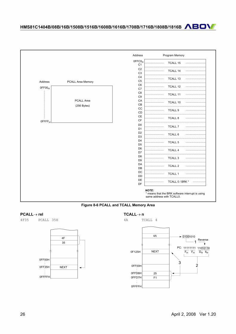
Page Call (PCALL) area contains subroutine program to reduceprogram byte length by using 2 bytes PCALL instead of 3 bytesCALL instruction. If it is frequently called, it is more useful tosave program byte length.
Table Call (TCALL) causes the CPU to jump to each TCALL ad-dress, where it commences the execution of the service routine.The Table Call service area spaces 2-byte for every TCALL:0FFC0H for TCALL15, 0FFC2H for TCALL14, etc., as shown inFigure 8-6.
Example: Usage of TCALL
The interrupt causes the CPU to jump to specific location, whereit commences the execution of the service routine. The Externalinterrupt 0, for example, is assigned to location 0FFFAH. The in-terrupt service locations spaces 2-byte interval: 0FFF8H and0FFF9H for External Interrupt 1, 0FFFAH and 0FFFBH for Exter-nal Interrupt 0, etc.
As for the area from 0FF00H to 0FFFFH, if any area of them is notgoing to be used, its service location is available as general pur-pose Program Memory.
Figure 8-5 Interrupt Vector Area
PROGRAMMEMORY
TCALLAREA
INTERRUPTVECTOR AREA
E000H
FEFFHFF00H
FFC0H
FFDFHFFE0H
FFFFH
PCALLAREA
F000H
HMS81C1X04B
HMS81C1X08B
C000H
HMS81C1X16B
LDA #5TCALL 0FH ;1BYTE INSTRUCTION: ;INSTEAD OF 3 BYTES: ;NORMAL CALL
;;TABLE CALL ROUTINE ;FUNC_A: LDA LRG0
RET;FUNC_B: LDA LRG1
RET;;TABLE CALL ADD. AREA;
ORG 0FFC0H ;TCALL ADDRESS AREADW FUNC_ADW FUNC_B
12
0FFE0H
E2
Address Vector Area Memory
E4E6E8EAECEEF0
F2F4F6F8FAFC
FE
--
Serial Peripheral Interface Interrupt Vector AreaBasic Interval Interrupt Vector Area
A/D Converter Interrupt Vector AreaTimer/Counter 3 Interrupt Vector AreaTimer/Counter 2 Interrupt Vector Area
External Interrupt 2 Vector AreaTimer/Counter 1 Interrupt Vector AreaTimer/Counter 0 Interrupt Vector Area
External Interrupt 0 Vector Area-
RESET Vector Area
External Interrupt 1 Vector Area
External Interrupt 3 Vector Area
Watchdog Timer Interrupt Vector Area
“-” means reserved area.NOTE:
April 2, 2008 Ver 1.20 25
HMS81C1404B/08B/16B/1508B/1516B/1608B/1616B/1708B/1716B/1808B/1816B
Figure 8-6 PCALL and TCALL Memory Area
PCALL→ rel4F35 PCALL 35H
TCALL→ n4A TCALL 4
0FFC0HC1
Address Program Memory
C2C3C4C5C6C7C8
0FF00H
Address PCALL Area Memory
0FFFFH
PCALL Area
(256 Bytes)
* means that the BRK software interrupt is usingsame address with TCALL0.
NOTE:
TCALL 15
TCALL 14
TCALL 13
TCALL 12
TCALL 11
TCALL 10
TCALL 9
TCALL 8
TCALL 7
TCALL 6
TCALL 5
TCALL 4
TCALL 3
TCALL 2
TCALL 1
TCALL 0 / BRK *
C9CACBCCCDCECFD0D1D2D3D4D5D6D7D8D9DADBDCDDDEDF
4F
~~ ~~
NEXT
35
0FF35H
0FF00H
0FFFFH
11111111 11010110
01001010
PC:FH FH DH 6H
4A
~~ ~~
250FFD6H
0FF00H
0FFFFH
F1
NEXT
0FFD7H
1
23
0F125H
Reverse
26 April 2, 2008 Ver 1.20
HMS81C1404B/08B/16B/1508B/1516B/1608B/1616B/1708B/1716B/1808B/1816B
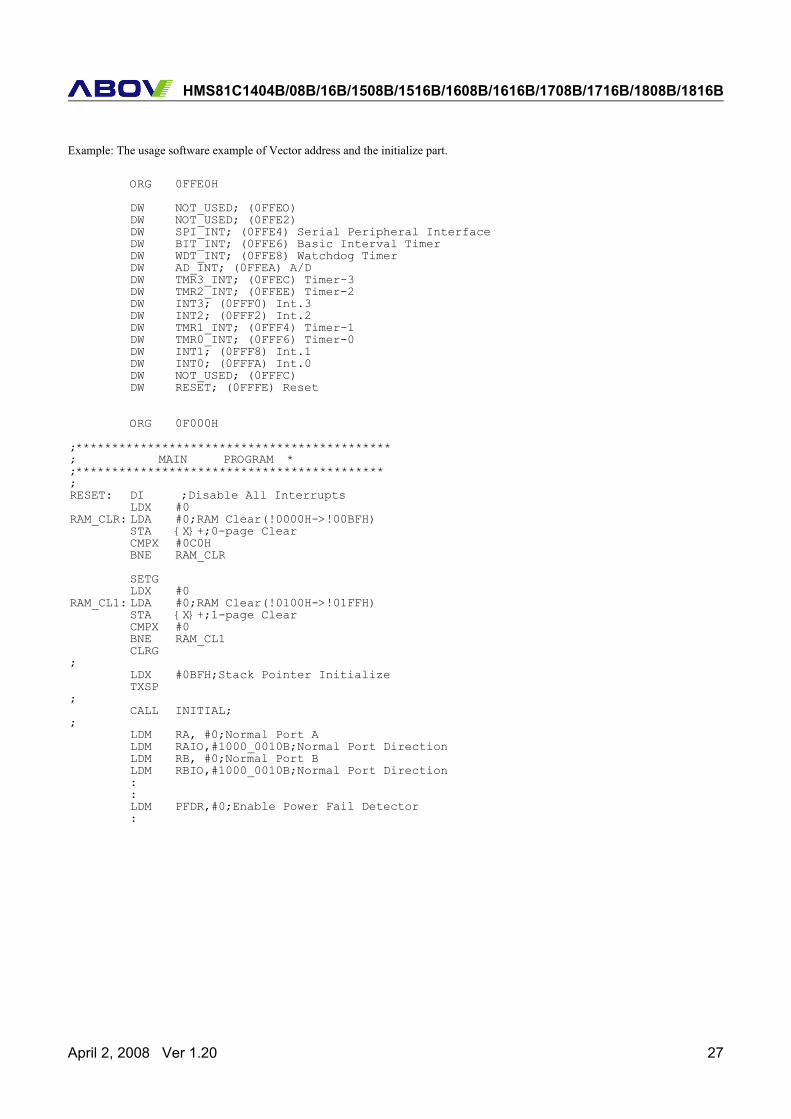
Example: The usage software example of Vector address and the initialize part.
ORG 0FFE0H
DW NOT_USED; (0FFEO)DW NOT_USED; (0FFE2)DW SPI_INT; (0FFE4) Serial Peripheral InterfaceDW BIT_INT; (0FFE6) Basic Interval TimerDW WDT_INT; (0FFE8) Watchdog TimerDW AD_INT; (0FFEA) A/DDW TMR3_INT; (0FFEC) Timer-3DW TMR2_INT; (0FFEE) Timer-2DW INT3; (0FFF0) Int.3DW INT2; (0FFF2) Int.2DW TMR1_INT; (0FFF4) Timer-1DW TMR0_INT; (0FFF6) Timer-0DW INT1; (0FFF8) Int.1DW INT0; (0FFFA) Int.0DW NOT_USED; (0FFFC) DW RESET; (0FFFE) Reset
ORG 0F000H
;********************************************; MAIN PROGRAM *;*******************************************;RESET: DI ;Disable All Interrupts
LDX #0RAM_CLR: LDA #0;RAM Clear(!0000H->!00BFH)
STA {X}+;0-page ClearCMPX #0C0HBNE RAM_CLR
SETGLDX #0
RAM_CL1: LDA #0;RAM Clear(!0100H->!01FFH)STA {X}+;1-page ClearCMPX #0BNE RAM_CL1CLRG
;LDX #0BFH;Stack Pointer InitializeTXSP
;CALL INITIAL;
;LDM RA, #0;Normal Port ALDM RAIO,#1000_0010B;Normal Port DirectionLDM RB, #0;Normal Port BLDM RBIO,#1000_0010B;Normal Port Direction::LDM PFDR,#0;Enable Power Fail Detector:
April 2, 2008 Ver 1.20 27
HMS81C1404B/08B/16B/1508B/1516B/1608B/1616B/1708B/1716B/1808B/1816B
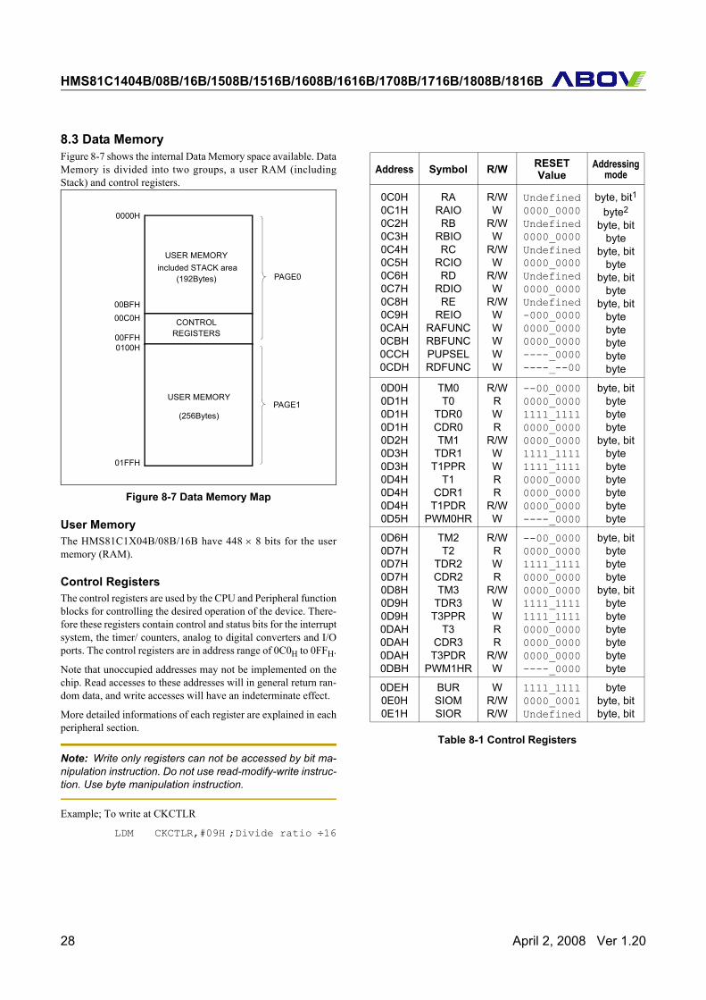
8.3 Data MemoryFigure 8-7 shows the internal Data Memory space available. DataMemory is divided into two groups, a user RAM (includingStack) and control registers.
Figure 8-7 Data Memory Map
User MemoryThe HMS81C1X04B/08B/16B have 448 × 8 bits for the usermemory (RAM).
Control RegistersThe control registers are used by the CPU and Peripheral functionblocks for controlling the desired operation of the device. There-fore these registers contain control and status bits for the interruptsystem, the timer/ counters, analog to digital converters and I/Oports. The control registers are in address range of 0C0H to 0FFH.
Note that unoccupied addresses may not be implemented on thechip. Read accesses to these addresses will in general return ran-dom data, and write accesses will have an indeterminate effect.
More detailed informations of each register are explained in eachperipheral section.
Note: Write only registers can not be accessed by bit ma-nipulation instruction. Do not use read-modify-write instruc-tion. Use byte manipulation instruction.
Example; To write at CKCTLR
LDM CKCTLR,#09H ;Divide ratio ÷16
USER MEMORY
CONTROLREGISTERS
0000H
00BFH00C0H
00FFH
PAGE0(192Bytes)
USER MEMORYPAGE1
0100H
01FFH
(256Bytes)
included STACK area
Address Symbol R/W RESET Value
Addressingmode
0C0H0C1H0C2H0C3H0C4H0C5H0C6H0C7H0C8H0C9H0CAH0CBH0CCH0CDH
RARAIORB
RBIORC
RCIORD
RDIORE
REIORAFUNCRBFUNCPUPSELRDFUNC
R/WW
R/WW
R/WW
R/WW
R/WWWWWW
Undefined0000_0000Undefined0000_0000Undefined0000_0000Undefined0000_0000Undefined-000_00000000_00000000_0000----_0000----_--00
byte, bit1
byte2
byte, bitbyte
byte, bitbyte
byte, bitbyte
byte, bitbytebytebytebytebyte
0D0H0D1H0D1H0D1H0D2H0D3H0D3H0D4H0D4H0D4H0D5H
TM0T0
TDR0CDR0TM1
TDR1T1PPR
T1CDR1
T1PDRPWM0HR
R/WRWR
R/WWWRR
R/WW
--00_00000000_00001111_11110000_00000000_00001111_11111111_11110000_00000000_00000000_0000----_0000
byte, bitbytebytebyte
byte, bitbytebytebytebytebytebyte
0D6H0D7H0D7H0D7H0D8H0D9H0D9H0DAH0DAH0DAH0DBH
TM2T2
TDR2CDR2TM3
TDR3T3PPR
T3CDR3
T3PDRPWM1HR
R/WRWR
R/WWWRR
R/WW
--00_00000000_00001111_11110000_00000000_00001111_11111111_11110000_00000000_00000000_0000----_0000
byte, bitbytebytebyte
byte, bitbytebytebytebytebytebyte
0DEH0E0H0E1H
BURSIOMSIOR
WR/WR/W
1111_11110000_0001Undefined
bytebyte, bitbyte, bit
Table 8-1 Control Registers
28 April 2, 2008 Ver 1.20
HMS81C1404B/08B/16B/1508B/1516B/1608B/1616B/1708B/1716B/1808B/1816B
Note: Several names are given at same address. Refer to
below table.
Stack AreaThe stack provides the area where the return address is saved be-fore a jump is performed during the processing routine at the ex-ecution of a subroutine call instruction or the acceptance of aninterrupt.
When returning from the processing routine, executing the sub-routine return instruction [RET] restores the contents of the pro-gram counter from the stack; executing the interrupt returninstruction [RETI] restores the contents of the program counterand flags.
The save/restore locations in the stack are determined by thestack pointed (SP). The SP is automatically decreased after thesaving, and increased before the restoring. This means the valueof the SP indicates the stack location number for the next save.
0E2H0E3H0E4H0E5H0E6H0EAH0EBH0ECH0ECH0EDH0EDH0EFH
IENHIENLIRQHIRQLIEDS
ADCMADCRBITR
CKCTLRWDTRWDTRPFDR
R/WR/WR/WR/WR/WR/W
RRWRW
R/W
0000_00000000_----0000_00000000_----0000_0000--00_0001Undefined0000_0000-001_01110000_00000111_1111----_-100
byte, bitbyte, bitbyte, bitbyte, bitbyte, bitbyte, bit
bytebytebytebytebyte
byte, bit
1. “byte, bit” means that register can be addressed by not only bit but byte manipulation instruction.
2. “byte” means that register can be addressed by only byte manipulation instruction. On the other hand, do not use any read-modify-write instruction such as bit manipulation for clearing bit.
Table 8-1 Control Registers
Addr.When read When write
Timer Mode
Capture Mode
PWM Mode
Timer Mode
PWM Mode
D1H T0 CDR0 - TDR0 -
D3H - TDR1 T1PPR
D4H T1 CDR1 T1PDR - T1PDR
D7H T2 CDR2 - TDR2 -
D9H - TDR3 T3PPR
DAH T3 CDR3 T3PDR - T3PDR
ECH BITR CKCTLR
Table 8-2 Various Register Name in Same Address
April 2, 2008 Ver 1.20 29
HMS81C1404B/08B/16B/1508B/1516B/1608B/1616B/1708B/1716B/1808B/1816B
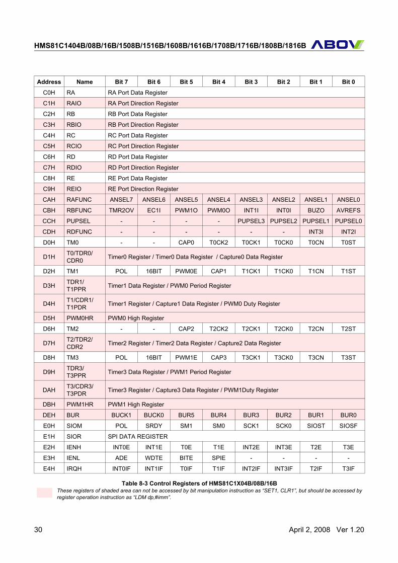
Address Name Bit 7 Bit 6 Bit 5 Bit 4 Bit 3 Bit 2 Bit 1 Bit 0
C0H RA RA Port Data Register
C1H RAIO RA Port Direction Register
C2H RB RB Port Data Register
C3H RBIO RB Port Direction Register
C4H RC RC Port Data Register
C5H RCIO RC Port Direction Register
C6H RD RD Port Data Register
C7H RDIO RD Port Direction Register
C8H RE RE Port Data Register
C9H REIO RE Port Direction Register
CAH RAFUNC ANSEL7 ANSEL6 ANSEL5 ANSEL4 ANSEL3 ANSEL2 ANSEL1 ANSEL0
CBH RBFUNC TMR2OV EC1I PWM1O PWM0O INT1I INT0I BUZO AVREFS
CCH PUPSEL - - - - PUPSEL3 PUPSEL2 PUPSEL1 PUPSEL0
CDH RDFUNC - - - - - - INT3I INT2I
D0H TM0 - - CAP0 T0CK2 T0CK1 T0CK0 T0CN T0ST
D1H T0/TDR0/CDR0 Timer0 Register / Timer0 Data Register / Capture0 Data Register
D2H TM1 POL 16BIT PWM0E CAP1 T1CK1 T1CK0 T1CN T1ST
D3H TDR1/T1PPR Timer1 Data Register / PWM0 Period Register
D4H T1/CDR1/T1PDR Timer1 Register / Capture1 Data Register / PWM0 Duty Register
D5H PWM0HR PWM0 High Register
D6H TM2 - - CAP2 T2CK2 T2CK1 T2CK0 T2CN T2ST
D7H T2/TDR2/CDR2 Timer2 Register / Timer2 Data Register / Capture2 Data Register
D8H TM3 POL 16BIT PWM1E CAP3 T3CK1 T3CK0 T3CN T3ST
D9H TDR3/T3PPR Timer3 Data Register / PWM1 Period Register
DAH T3/CDR3/T3PDR Timer3 Register / Capture3 Data Register / PWM1Duty Register
DBH PWM1HR PWM1 High Register
DEH BUR BUCK1 BUCK0 BUR5 BUR4 BUR3 BUR2 BUR1 BUR0
E0H SIOM POL SRDY SM1 SM0 SCK1 SCK0 SIOST SIOSF
E1H SIOR SPI DATA REGISTER
E2H IENH INT0E INT1E T0E T1E INT2E INT3E T2E T3E
E3H IENL ADE WDTE BITE SPIE - - - -
E4H IRQH INT0IF INT1IF T0IF T1IF INT2IF INT3IF T2IF T3IF
Table 8-3 Control Registers of HMS81C1X04B/08B/16BThese registers of shaded area can not be accessed by bit manipulation instruction as “SET1, CLR1”, but should be accessed by register operation instruction as “LDM dp,#imm”.
30 April 2, 2008 Ver 1.20
HMS81C1404B/08B/16B/1508B/1516B/1608B/1616B/1708B/1716B/1808B/1816B
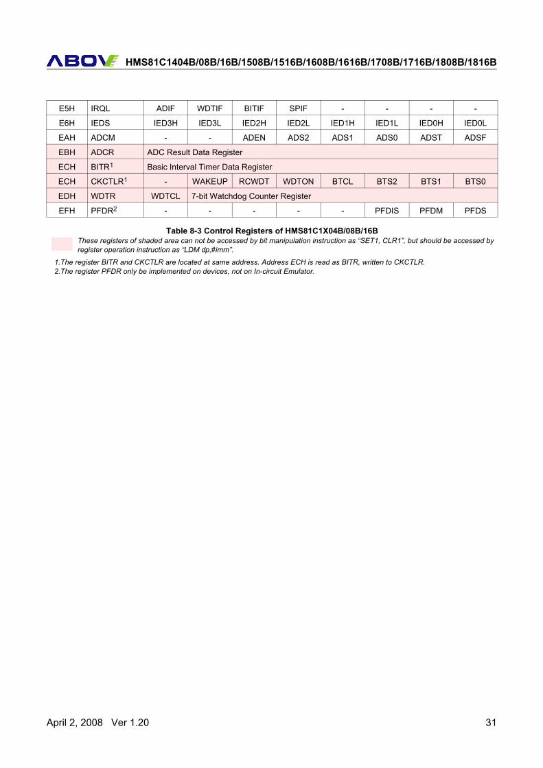
E5H IRQL ADIF WDTIF BITIF SPIF - - - -
E6H IEDS IED3H IED3L IED2H IED2L IED1H IED1L IED0H IED0L
EAH ADCM - - ADEN ADS2 ADS1 ADS0 ADST ADSF
EBH ADCR ADC Result Data Register
ECH BITR1 Basic Interval Timer Data Register
ECH CKCTLR1 - WAKEUP RCWDT WDTON BTCL BTS2 BTS1 BTS0
EDH WDTR WDTCL 7-bit Watchdog Counter Register
EFH PFDR2 - - - - - PFDIS PFDM PFDS
1.The register BITR and CKCTLR are located at same address. Address ECH is read as BITR, written to CKCTLR.2.The register PFDR only be implemented on devices, not on In-circuit Emulator.
Table 8-3 Control Registers of HMS81C1X04B/08B/16BThese registers of shaded area can not be accessed by bit manipulation instruction as “SET1, CLR1”, but should be accessed by register operation instruction as “LDM dp,#imm”.
April 2, 2008 Ver 1.20 31
HMS81C1404B/08B/16B/1508B/1516B/1608B/1616B/1708B/1716B/1808B/1816B
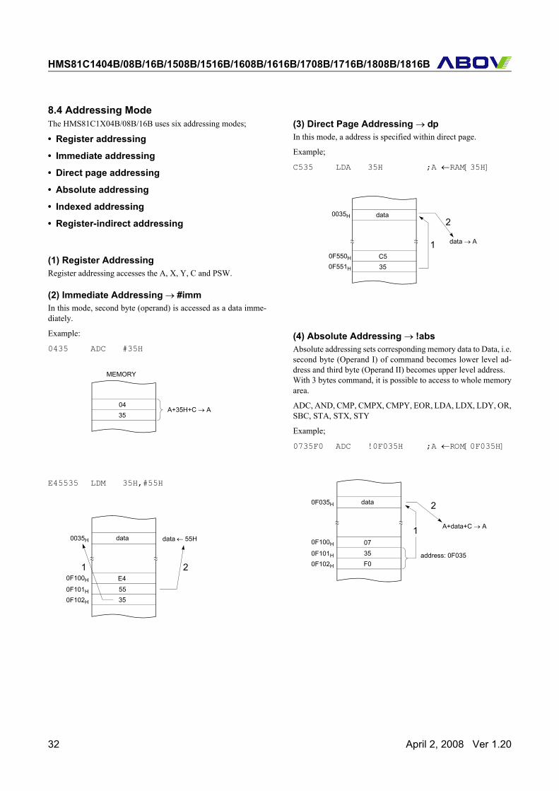
8.4 Addressing ModeThe HMS81C1X04B/08B/16B uses six addressing modes;
• Register addressing
• Immediate addressing
• Direct page addressing
• Absolute addressing
• Indexed addressing
• Register-indirect addressing
(1) Register AddressingRegister addressing accesses the A, X, Y, C and PSW.
(2) Immediate Addressing → #immIn this mode, second byte (operand) is accessed as a data imme-diately.
Example:
0435 ADC #35H
E45535 LDM 35H,#55H
(3) Direct Page Addressing → dpIn this mode, a address is specified within direct page.
Example;
C535 LDA 35H ;A ←RAM[35H]
(4) Absolute Addressing → !absAbsolute addressing sets corresponding memory data to Data, i.e.second byte (Operand I) of command becomes lower level ad-dress and third byte (Operand II) becomes upper level address.With 3 bytes command, it is possible to access to whole memoryarea.
ADC, AND, CMP, CMPX, CMPY, EOR, LDA, LDX, LDY, OR,SBC, STA, STX, STY
Example;
0735F0 ADC !0F035H ;A ←ROM[0F035H]
35A+35H+C → A
04
MEMORY
E40F100H
data ← 55H
~~ ~~
data0035H
1
350F102H
550F101H
2
data
35
0035H
0F551H
data → A
2
1~~ ~~
C50F550H
070F100H
~~ ~~
data0F035H
1
F00F102H
350F101H
2
A+data+C → A
address: 0F035
32 April 2, 2008 Ver 1.20
HMS81C1404B/08B/16B/1508B/1516B/1608B/1616B/1708B/1716B/1808B/1816B
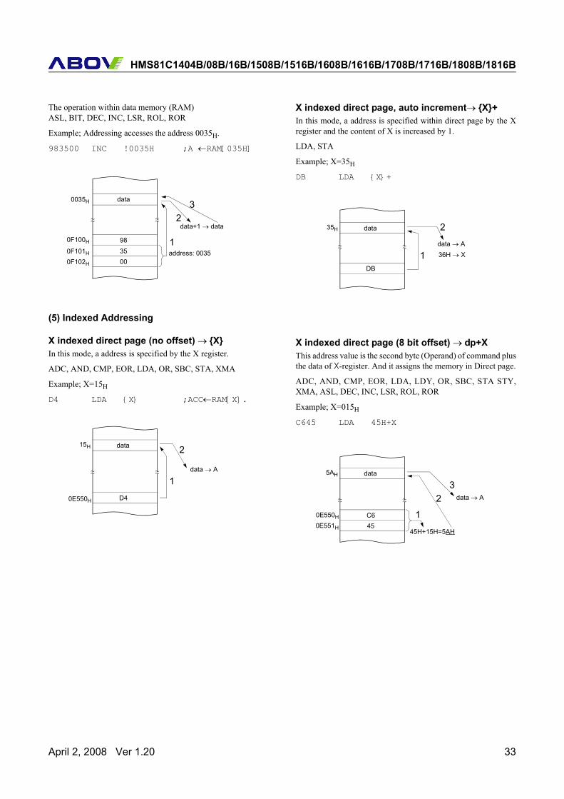
The operation within data memory (RAM)ASL, BIT, DEC, INC, LSR, ROL, ROR
Example; Addressing accesses the address 0035H.
983500 INC !0035H ;A ←RAM[035H]
(5) Indexed Addressing
X indexed direct page (no offset) → {X}In this mode, a address is specified by the X register.
ADC, AND, CMP, EOR, LDA, OR, SBC, STA, XMA
Example; X=15H
D4 LDA {X} ;ACC←RAM[X].
X indexed direct page, auto increment→ {X}+In this mode, a address is specified within direct page by the Xregister and the content of X is increased by 1.
LDA, STA
Example; X=35H
DB LDA {X}+
X indexed direct page (8 bit offset) → dp+XThis address value is the second byte (Operand) of command plusthe data of X-register. And it assigns the memory in Direct page.
ADC, AND, CMP, EOR, LDA, LDY, OR, SBC, STA STY,XMA, ASL, DEC, INC, LSR, ROL, ROR
Example; X=015H
C645 LDA 45H+X
980F100H
~~ ~~
data0035H
1
000F102H
350F101H
2data+1 → data
3
address: 0035
data
D4
15H
0E550H
data → A
2
1~~ ~~
data
DB
35H
data → A
2
1~~ ~~
36H → X
data
45
5AH
0E551H
data → A2
1
~~ ~~
C60E550H
45H+15H=5AH
3
April 2, 2008 Ver 1.20 33
HMS81C1404B/08B/16B/1508B/1516B/1608B/1616B/1708B/1716B/1808B/1816B
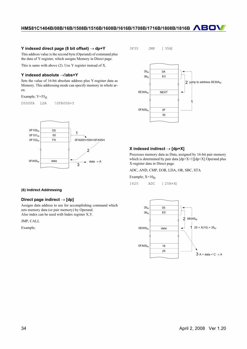
Y indexed direct page (8 bit offset) → dp+YThis address value is the second byte (Operand) of command plusthe data of Y-register, which assigns Memory in Direct page.
This is same with above (2). Use Y register instead of X.
Y indexed absolute →!abs+YSets the value of 16-bit absolute address plus Y-register data asMemory. This addressing mode can specify memory in whole ar-ea.
Example; Y=55H
D500FA LDA !0FA00H+Y
(6) Indirect Addressing
Direct page indirect → [dp]Assigns data address to use for accomplishing command whichsets memory data (or pair memory) by Operand.Also index can be used with Index register X,Y.
JMP, CALL
Example;
3F35 JMP [35H]
X indexed indirect → [dp+X]Processes memory data as Data, assigned by 16-bit pair memorywhich is determined by pair data [dp+X+1][dp+X] Operand plusX-register data in Direct page.
ADC, AND, CMP, EOR, LDA, OR, SBC, STA
Example; X=10H
1625 ADC [25H+X]
D50F100H
data → A
1
~~ ~~
data0FA55H
0FA00H+55H=0FA55H
3
FA0F102H
000F101H
2
0A35H
jump to address 0E30AH
1
~~ ~~
35
0FA00H
E336H
2
3F
0E30AH NEXT
~~ ~~
0535H
0E005H~~ ~~
25
0FA00H
E036H
16
0E005H data
~~ ~~
3 A + data + C → A
25 + X(10) = 35H1
2
34 April 2, 2008 Ver 1.20
HMS81C1404B/08B/16B/1508B/1516B/1608B/1616B/1708B/1716B/1808B/1816B
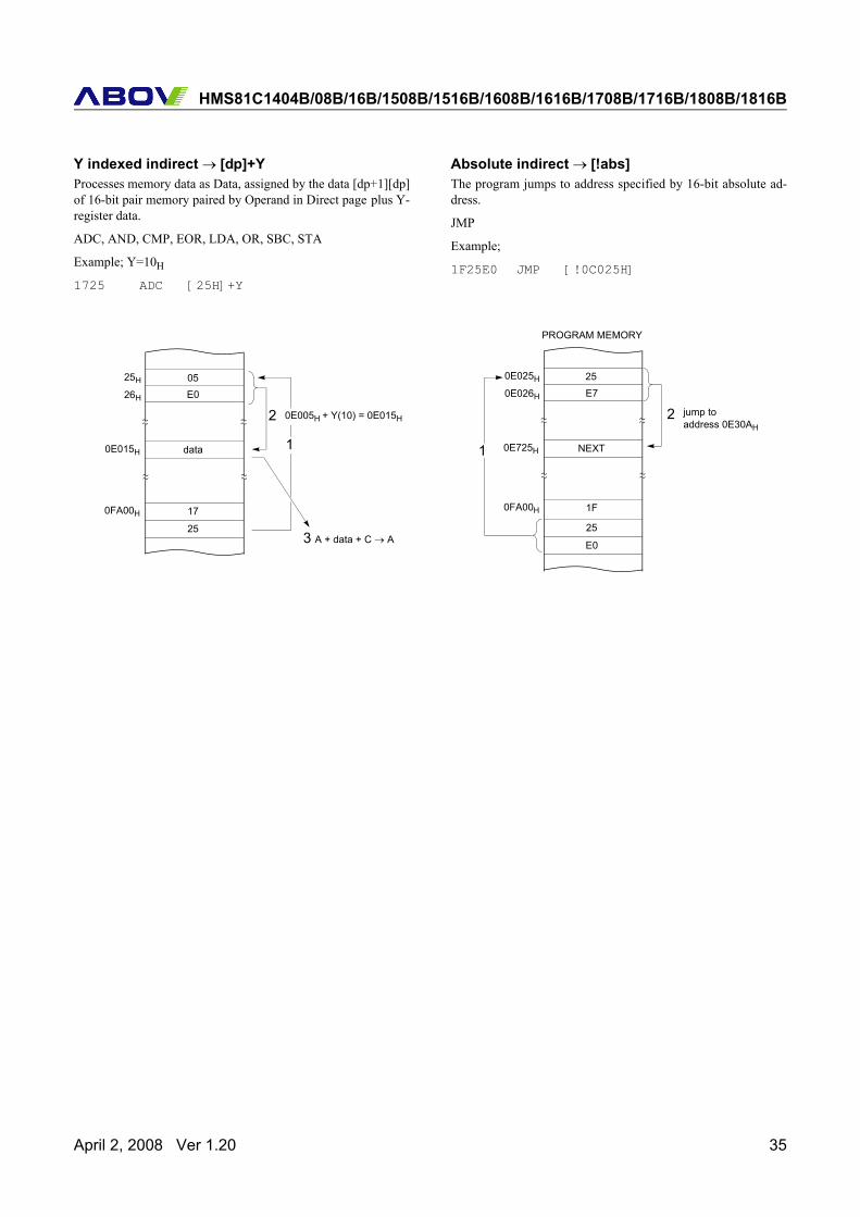
Y indexed indirect → [dp]+YProcesses memory data as Data, assigned by the data [dp+1][dp]of 16-bit pair memory paired by Operand in Direct page plus Y-register data.
ADC, AND, CMP, EOR, LDA, OR, SBC, STA
Example; Y=10H
1725 ADC [25H]+Y
Absolute indirect → [!abs]The program jumps to address specified by 16-bit absolute ad-dress.
JMP
Example;
1F25E0 JMP [!0C025H]
0525H
0E005H + Y(10) = 0E015H
1
~~ ~~
25
0FA00H
E026H
2
17
0E015H data
~~ ~~
3 A + data + C → A
250E025H
jump to~~ ~~
E0
0FA00H
E70E026H
2
25
0E725H NEXT
~~ ~~
1F
PROGRAM MEMORY
1
address 0E30AH
April 2, 2008 Ver 1.20 35
HMS81C1404B/08B/16B/1508B/1516B/1608B/1616B/1708B/1716B/1808B/1816B
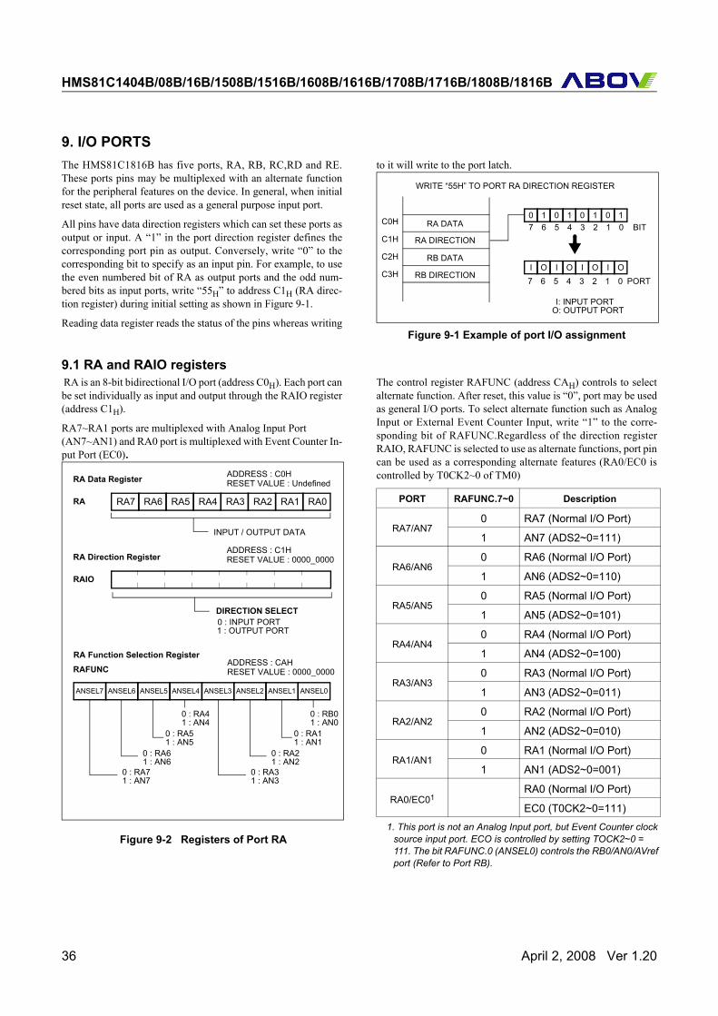
9. I/O PORTSThe HMS81C1816B has five ports, RA, RB, RC,RD and RE.These ports pins may be multiplexed with an alternate functionfor the peripheral features on the device. In general, when initialreset state, all ports are used as a general purpose input port.
All pins have data direction registers which can set these ports asoutput or input. A “1” in the port direction register defines thecorresponding port pin as output. Conversely, write “0” to thecorresponding bit to specify as an input pin. For example, to usethe even numbered bit of RA as output ports and the odd num-bered bits as input ports, write “55H” to address C1H (RA direc-tion register) during initial setting as shown in Figure 9-1.
Reading data register reads the status of the pins whereas writing
to it will write to the port latch.
Figure 9-1 Example of port I/O assignment
9.1 RA and RAIO registers RA is an 8-bit bidirectional I/O port (address C0H). Each port canbe set individually as input and output through the RAIO register(address C1H).
RA7~RA1 ports are multiplexed with Analog Input Port(AN7~AN1) and RA0 port is multiplexed with Event Counter In-put Port (EC0).
Figure 9-2 Registers of Port RA
The control register RAFUNC (address CAH) controls to selectalternate function. After reset, this value is “0”, port may be usedas general I/O ports. To select alternate function such as AnalogInput or External Event Counter Input, write “1” to the corre-sponding bit of RAFUNC.Regardless of the direction registerRAIO, RAFUNC is selected to use as alternate functions, port pincan be used as a corresponding alternate features (RA0/EC0 iscontrolled by T0CK2~0 of TM0)
I: INPUT PORT
WRITE “55H” TO PORT RA DIRECTION REGISTER
0 1 0 1 0 1 0 1
I O I O I O I O
RA DATA
RB DATA
RA DIRECTION
RB DIRECTION
C0H
C1H
C2H
C3H
7 6 5 4 3 2 1 0 BIT
7 6 5 4 3 2 1 0 PORT
O: OUTPUT PORT
RA7 RA6 RA5 RA4 RA3 RA2 RA1 RA0
INPUT / OUTPUT DATA
0 : INPUT PORT1 : OUTPUT PORT
DIRECTION SELECT
RA Data Register
RA
ADDRESS : C0HRESET VALUE : Undefined
RA Direction Register
RAIO
ADDRESS : C1HRESET VALUE : 0000_0000
ANSEL0
RA Function Selection Register
RAFUNCADDRESS : CAHRESET VALUE : 0000_0000
ANSEL7 ANSEL1ANSEL2ANSEL3ANSEL4ANSEL5ANSEL6
0 : RB01 : AN0
0 : RA11 : AN1
0 : RA21 : AN2
0 : RA31 : AN3
0 : RA41 : AN4
0 : RA51 : AN5
0 : RA61 : AN6
0 : RA71 : AN7
PORT RAFUNC.7~0 Description
RA7/AN70 RA7 (Normal I/O Port)
1 AN7 (ADS2~0=111)
RA6/AN60 RA6 (Normal I/O Port)
1 AN6 (ADS2~0=110)
RA5/AN50 RA5 (Normal I/O Port)
1 AN5 (ADS2~0=101)
RA4/AN40 RA4 (Normal I/O Port)
1 AN4 (ADS2~0=100)
RA3/AN30 RA3 (Normal I/O Port)
1 AN3 (ADS2~0=011)
RA2/AN20 RA2 (Normal I/O Port)
1 AN2 (ADS2~0=010)
RA1/AN10 RA1 (Normal I/O Port)
1 AN1 (ADS2~0=001)
RA0/EC01
1. This port is not an Analog Input port, but Event Counter clock source input port. ECO is controlled by setting TOCK2~0 = 111. The bit RAFUNC.0 (ANSEL0) controls the RB0/AN0/AVref port (Refer to Port RB).
RA0 (Normal I/O Port)
EC0 (T0CK2~0=111)
36 April 2, 2008 Ver 1.20
HMS81C1404B/08B/16B/1508B/1516B/1608B/1616B/1708B/1716B/1808B/1816B
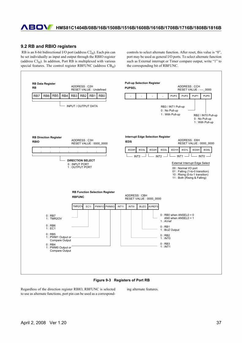
9.2 RB and RBIO registers RB is an 8-bit bidirectional I/O port (address C2H). Each pin canbe set individually as input and output through the RBIO register(address C3H). In addition, Port RB is multiplexed with variousspecial features. The control register RBFUNC (address CBH)
controls to select alternate function. After reset, this value is “0”,port may be used as general I/O ports. To select alternate functionsuch as External interrupt or Timer compare output, write “1” tothe corresponding bit of RBFUNC.
Figure 9-3 Registers of Port RB
Regardless of the direction register RBIO, RBFUNC is selectedto use as alternate functions, port pin can be used as a correspond-
ing alternate features.
RB5 RB4 RB3 RB2 RB1 RB0
INPUT / OUTPUT DATA
0 : INPUT PORT1 : OUTPUT PORT
DIRECTION SELECT
RB Data RegisterRB ADDRESS : C2H
RESET VALUE : Undefined
RB Direction RegisterRBIO ADDRESS : C3H
RESET VALUE : 0000_0000
AVREFS
RB Function Selection RegisterRBFUNC ADDRESS : CBH
RESET VALUE : 0000_0000
BUZOINT0IINT1IPWM0O
0 : RB0 when ANSEL0 = 0
1 : AVref
0 : RB11 : BUZ Output
0 : RB41 : PWM0 Output or
0 : RB21 : INT0
0 : RB31 : INT1
PUP0
Pull-up Selection Register
PUPSEL ADDRESS : CCHRESET VALUE : ----_0000
- PUP1-- -
0 : No Pull-up1 : With Pull-up
0 : No Pull-up1 : With Pull-up
IED0L
Interrupt Edge Selection Register
IEDS ADDRESS : E6HRESET VALUE : 0000_0000
IED0HIED1LIED1H
External Interrupt Edge Select
INT0INT1
00 : Normal I/O port01 : Falling (1-to-0 transition)10 : Rising (0-to-1 transition)11 : Both (Rising & Falling)
Compare Output
RB2 / INT0 Pull-up
RB3 / INT1 Pull-up
AN0 when ANSEL0 = 1
RB6RB7
PWM1OTMR2OV EC1I
IED2LIED2HIED3LIED3H
INT2INT3
0 : RB51 : PWM1 Output or Compare Output
0 : RB61 : EC1
0 : RB71 : TMR2OV
PUP2PUP3
April 2, 2008 Ver 1.20 37
HMS81C1404B/08B/16B/1508B/1516B/1608B/1616B/1708B/1716B/1808B/1816B
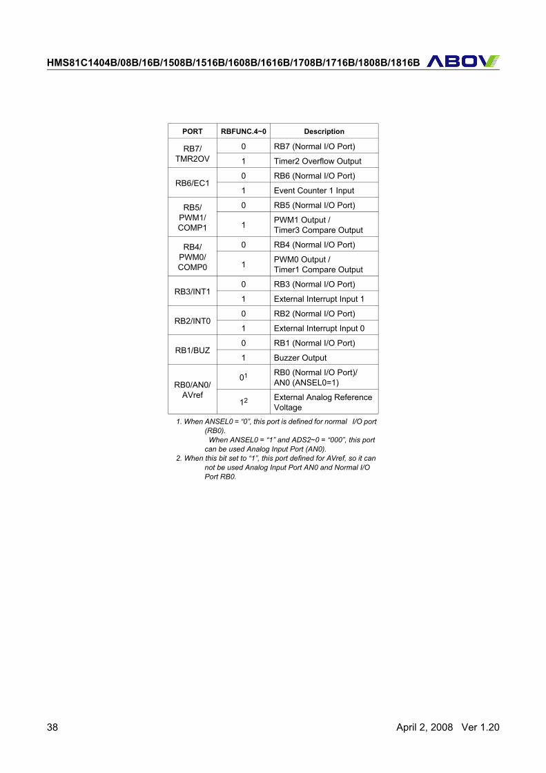
PORT RBFUNC.4~0 Description
RB7/TMR2OV
0 RB7 (Normal I/O Port)
1 Timer2 Overflow Output
RB6/EC10 RB6 (Normal I/O Port)
1 Event Counter 1 Input
RB5/PWM1/COMP1
0 RB5 (Normal I/O Port)
1 PWM1 Output / Timer3 Compare Output
RB4/PWM0/COMP0
0 RB4 (Normal I/O Port)
1 PWM0 Output / Timer1 Compare Output
RB3/INT10 RB3 (Normal I/O Port)
1 External Interrupt Input 1
RB2/INT00 RB2 (Normal I/O Port)
1 External Interrupt Input 0
RB1/BUZ0 RB1 (Normal I/O Port)
1 Buzzer Output
RB0/AN0/AVref
01
1. When ANSEL0 = “0”, this port is defined for normal I/O port (RB0).
When ANSEL0 = “1” and ADS2~0 = “000”, this port can be used Analog Input Port (AN0).
RB0 (Normal I/O Port)/ AN0 (ANSEL0=1)
12
2. When this bit set to “1”, this port defined for AVref, so it can not be used Analog Input Port AN0 and Normal I/O Port RB0.
External Analog Reference Voltage
38 April 2, 2008 Ver 1.20
HMS81C1404B/08B/16B/1508B/1516B/1608B/1616B/1708B/1716B/1808B/1816B
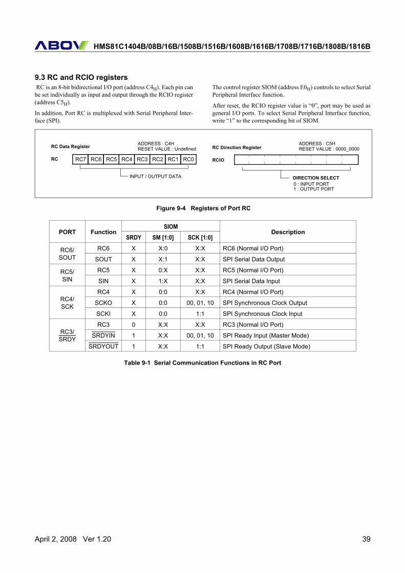
9.3 RC and RCIO registers RC is an 8-bit bidirectional I/O port (address C4H). Each pin canbe set individually as input and output through the RCIO register(address C5H).
In addition, Port RC is multiplexed with Serial Peripheral Inter-face (SPI).
The control register SIOM (address E0H) controls to select SerialPeripheral Interface function.
After reset, the RCIO register value is “0”, port may be used asgeneral I/O ports. To select Serial Peripheral Interface function,write “1” to the corresponding bit of SIOM.
Figure 9-4 Registers of Port RC
Table 9-1 Serial Communication Functions in RC Port
PORT FunctionSIOM
DescriptionSRDY SM [1:0] SCK [1:0]
RC6/SOUT
RC6 X X:0 X:X RC6 (Normal I/O Port)
SOUT X X:1 X:X SPI Serial Data Output
RC5/SIN
RC5 X 0:X X:X RC5 (Normal I/O Port)
SIN X 1:X X:X SPI Serial Data Input
RC4/SCK
RC4 X 0:0 X:X RC4 (Normal I/O Port)
SCKO X 0:0 00, 01, 10 SPI Synchronous Clock Output
SCKI X 0:0 1:1 SPI Synchronous Clock Input
RC3/SRDY
RC3 0 X:X X:X RC3 (Normal I/O Port)
SRDYIN 1 X:X 00, 01, 10 SPI Ready Input (Master Mode)
SRDYOUT 1 X:X 1:1 SPI Ready Output (Slave Mode)
INPUT / OUTPUT DATA0 : INPUT PORT1 : OUTPUT PORT
DIRECTION SELECT
RC Data Register
RC
ADDRESS : C4HRESET VALUE : Undefined RC Direction Register
RCIO
ADDRESS : C5HRESET VALUE : 0000_0000
RC6 RC5 RC4 RC3RC7 RC2 RC1 RC0
April 2, 2008 Ver 1.20 39
HMS81C1404B/08B/16B/1508B/1516B/1608B/1616B/1708B/1716B/1808B/1816B
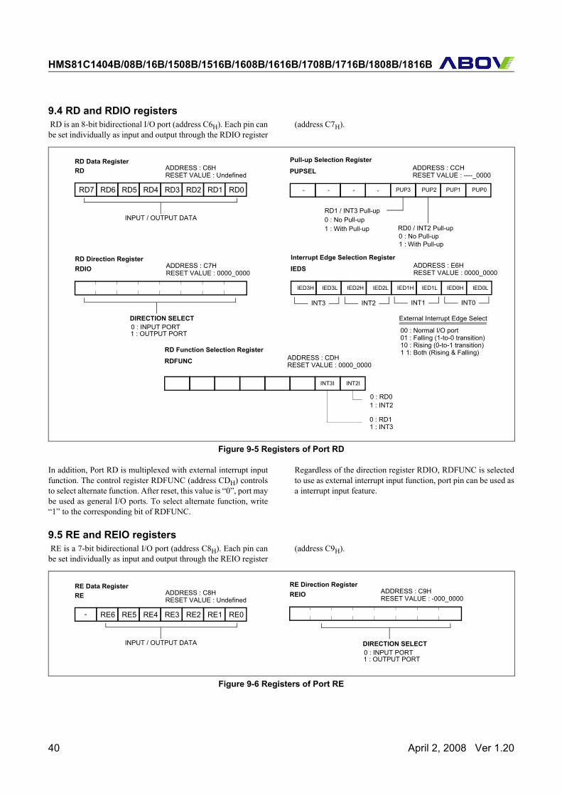
9.4 RD and RDIO registers RD is an 8-bit bidirectional I/O port (address C6H). Each pin canbe set individually as input and output through the RDIO register
(address C7H).
Figure 9-5 Registers of Port RD
In addition, Port RD is multiplexed with external interrupt inputfunction. The control register RDFUNC (address CDH) controlsto select alternate function. After reset, this value is “0”, port maybe used as general I/O ports. To select alternate function, write“1” to the corresponding bit of RDFUNC.
Regardless of the direction register RDIO, RDFUNC is selectedto use as external interrupt input function, port pin can be used asa interrupt input feature.
9.5 RE and REIO registers RE is a 7-bit bidirectional I/O port (address C8H). Each pin canbe set individually as input and output through the REIO register
(address C9H).
Figure 9-6 Registers of Port RE
RD2 RD1 RD0
INPUT / OUTPUT DATA
0 : INPUT PORT1 : OUTPUT PORT
DIRECTION SELECT
RD Data RegisterRD ADDRESS : C6H
RESET VALUE : Undefined
RD Direction RegisterRDIO ADDRESS : C7H
RESET VALUE : 0000_0000
INT2I
RD Function Selection RegisterRDFUNC ADDRESS : CDH
RESET VALUE : 0000_0000
INT3I
0 : RD01 : INT2
0 : RD11 : INT3
PUP0
Pull-up Selection Register
PUPSEL ADDRESS : CCHRESET VALUE : ----_0000
- PUP1-- -
0 : No Pull-up1 : With Pull-up
0 : No Pull-up1 : With Pull-up
IED0L
Interrupt Edge Selection RegisterIEDS ADDRESS : E6H
RESET VALUE : 0000_0000
IED0HIED1LIED1H
External Interrupt Edge Select
INT0INT1
00 : Normal I/O port01 : Falling (1-to-0 transition)10 : Rising (0-to-1 transition)1 1: Both (Rising & Falling)
RD0 / INT2 Pull-up
RD1 / INT3 Pull-up
IED2LIED2HIED3LIED3H
INT2INT3
PUP2PUP3RD3RD4RD5RD6RD7
RE2 RE1 RE0
INPUT / OUTPUT DATA0 : INPUT PORT1 : OUTPUT PORT
DIRECTION SELECT
RE Data RegisterRE ADDRESS : C8H
RESET VALUE : Undefined
RE Direction RegisterREIO ADDRESS : C9H
RESET VALUE : -000_0000
RE3RE4RE5RE6-
40 April 2, 2008 Ver 1.20
HMS81C1404B/08B/16B/1508B/1516B/1608B/1616B/1708B/1716B/1808B/1816B
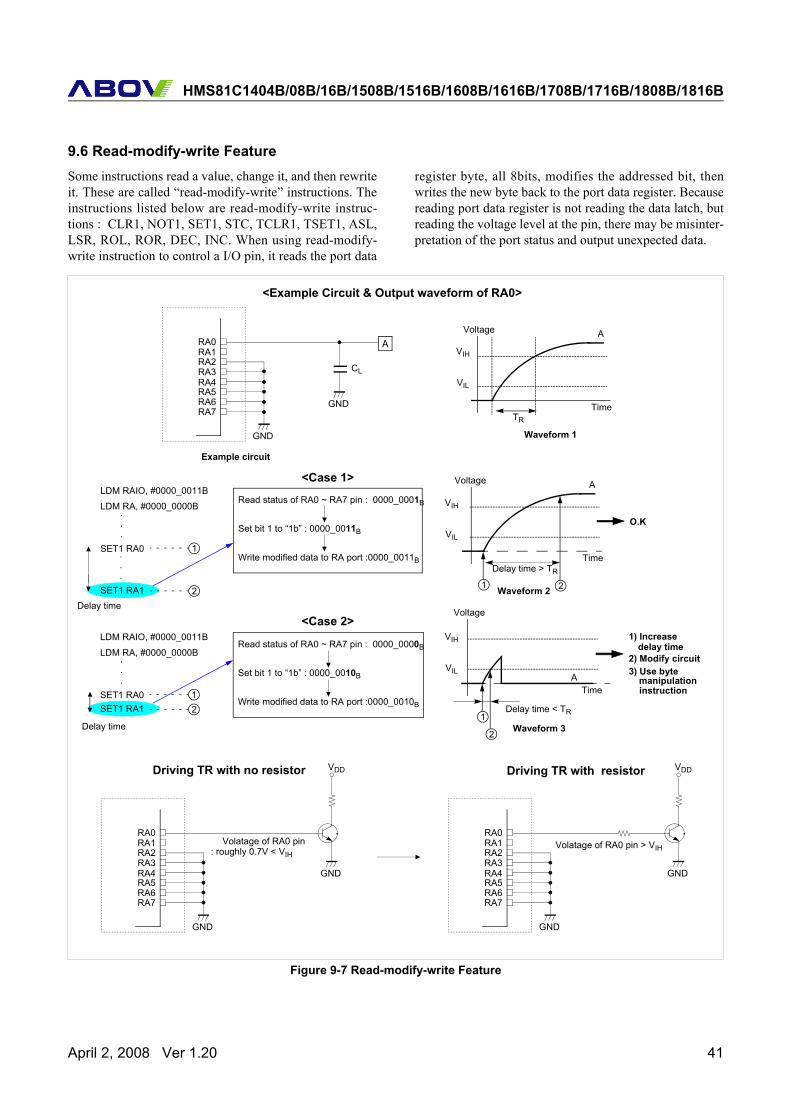
9.6 Read-modify-write FeatureSome instructions read a value, change it, and then rewriteit. These are called “read-modify-write” instructions. Theinstructions listed below are read-modify-write instruc-tions : CLR1, NOT1, SET1, STC, TCLR1, TSET1, ASL,LSR, ROL, ROR, DEC, INC. When using read-modify-write instruction to control a I/O pin, it reads the port data
register byte, all 8bits, modifies the addressed bit, thenwrites the new byte back to the port data register. Becausereading port data register is not reading the data latch, butreading the voltage level at the pin, there may be misinter-pretation of the port status and output unexpected data.
Figure 9-7 Read-modify-write Feature
SET1 RA0
LDM RA, #0000_0000B
SET1 RA1
.
.
.
LDM RAIO, #0000_0011B
A
CL
1
2
<Case 1>
.
.
.
SET1 RA0
LDM RA, #0000_0000B
SET1 RA1
.
.
.
LDM RAIO, #0000_0011B
12
<Case 2>
Read status of RA0 ~ RA7 pin : 0000_0001B
Set bit 1 to “1b” : 0000_0011B
Write modified data to RA port :0000_0011B
Read status of RA0 ~ RA7 pin : 0000_0000B
Set bit 1 to “1b” : 0000_0010B
Write modified data to RA port :0000_0010B
<Example Circuit & Output waveform of RA0>
Example circuit
Volatage of RA0 pin : roughly 0.7V < VIH
GND
VDD
RA0RA1RA2RA3RA4RA5RA6RA7
GND
RA0RA1RA2RA3RA4RA5RA6RA7
GND
GND
1
AVoltage
Time
AVoltage
Time
2
1
Voltage
Time
VIL
VIH
2
VIL
VIH
VIL
VIH
A
Waveform 1
Waveform 2
Waveform 3
TR
Delay time > TR
Delay time < TR
1) Increase delay time2) Modify circuit3) Use byte
O.K
manipulation instruction
Driving TR with no resistor
Volatage of RA0 pin > VIH
GND
VDD
RA0RA1RA2RA3RA4RA5RA6RA7
GND
Driving TR with resistor
Delay time
Delay time
April 2, 2008 Ver 1.20 41

HMS81C1404B/08B/16B/1508B/1516B/1608B/1616B/1708B/1716B/1808B/1816B
For example, as shown in Figure 9-7, if the capacitance ofthe CL is large enough to make considerably long risingtime, the port output may be like the waveform 1.
In case 1 of Figure 9-7, the RA0 outputs “1” because theread-modify-write instruction “SET1 RA1” is executedafter the voltage level of RA0 exceeds the VIH level(waveform2). But, in case 2, the RA0 outputs “0” becausethe read-modify-write instruction is executed before thevoltage level of RA0 reaches the VIL level (waveform3).
In the case that the rising or falling time of the pin is longerthan instruction execution time, it is necessary to add delaytime before read-modify-write instruction or modify cir-cuit to decrease the rising or falling time or use byte ma-nipulation instructions.
The misinterpretation of the port status may occur in theapplication of driving a transistor base without resistor. Itis recommended to insert a serial resistor between theMCU port and the transistor base pin in case of driving atransistor.
42 April 2, 2008 Ver 1.20
HMS81C1404B/08B/16B/1508B/1516B/1608B/1616B/1708B/1716B/1808B/1816B
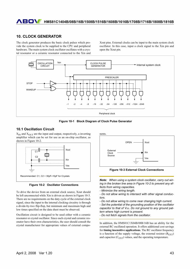
10. CLOCK GENERATORThe clock generator produces the basic clock pulses which pro-vide the system clock to be supplied to the CPU and peripheralhardware. The main system clock oscillator oscillates with a crys-tal resonator or a ceramic resonator connected to the Xin and
Xout pins. External clocks can be input to the main system clockoscillator. In this case, input a clock signal to the Xin pin andopen the Xout pin.
Figure 10-1 Block Diagram of Clock Pulse Generator
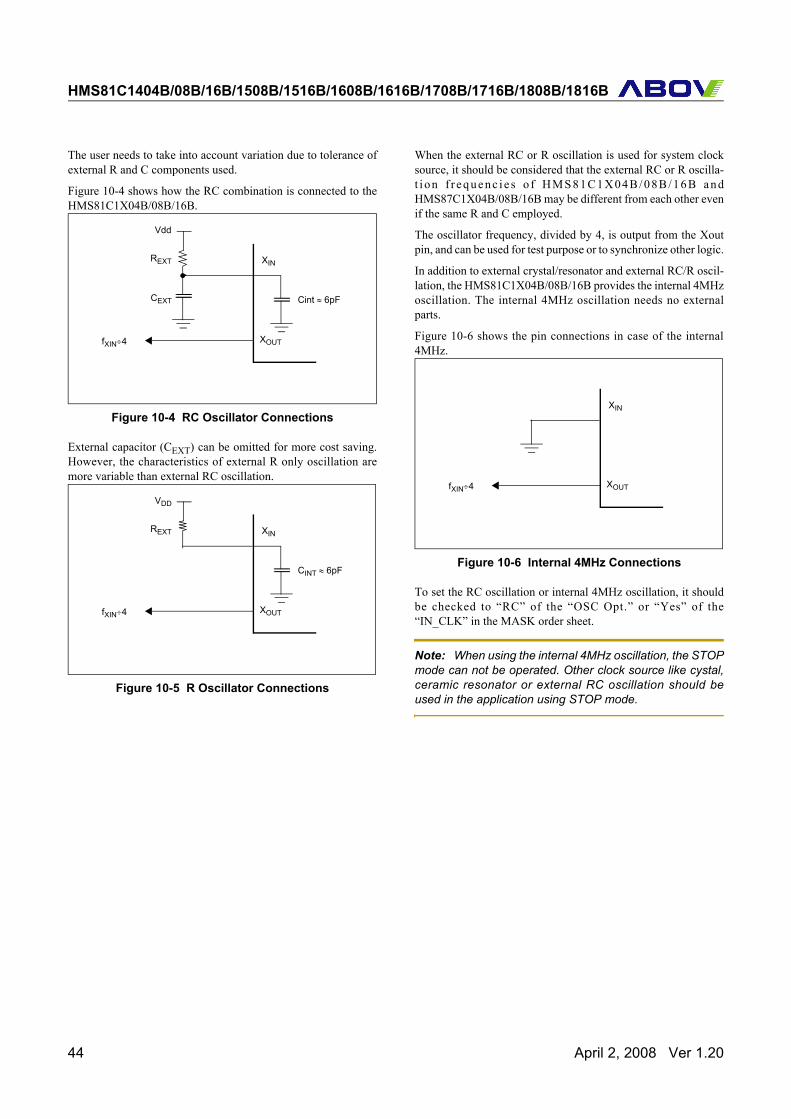
10.1 Oscillation CircuitXIN and XOUT are the input and output, respectively, a invertingamplifier which can be set for use as an on-chip oscillator, asshown in Figure 10-2.
Figure 10-2 Oscillator Connections
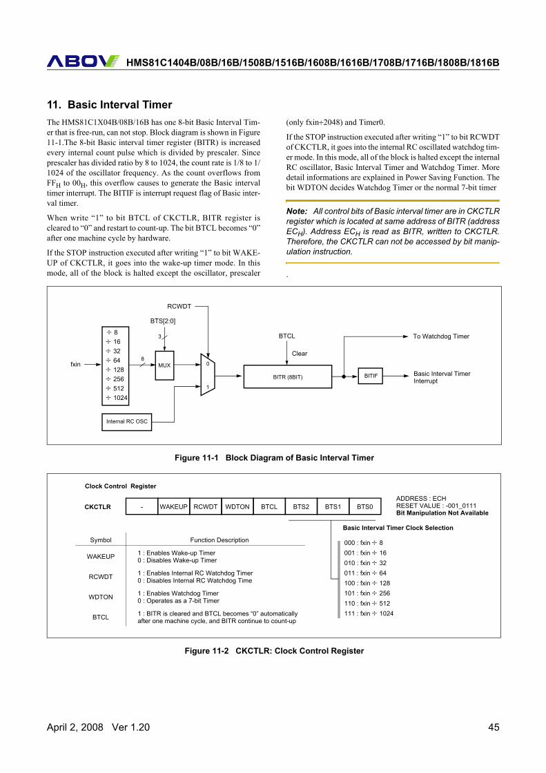
To drive the device from an external clock source, Xout shouldbe left unconnected while Xin is driven as shown in Figure 10-3.There are no requirements on the duty cycle of the external clocksignal, since the input to the internal clocking circuitry is througha divide-by-two flip-flop, but minimum and maximum high andlow times specified on the data sheet must be observed.
Oscillation circuit is designed to be used either with a ceramicresonator or crystal oscillator. Since each crystal and ceramic res-onator have their own characteristics, the user should consult thecrystal manufacturer for appropriate values of external compo-
nents.
Figure 10-3 External Clock Connections
Note: When using a system clock oscillator, carry out wir-ing in the broken line area in Figure 10-2 to prevent any ef-fects from wiring capacities.- Minimize the wiring length.- Do not allow wiring to intersect with other signal conduc-tors. - Do not allow wiring to come near changing high current.- Set the potential of the grounding position of the oscillatorcapacitor to that of VSS. Do not ground to any ground pat-tern where high current is present.- Do not fetch signals from the oscillator.
In addition, the HMS81C1X04B/08B/16B has an ability for theexternal RC oscillated operation. It offers additional cost savingsfor timing insensitive applications. The RC oscillator frequencyis a function of the supply voltage, the external resistor (REXT)and capacitor (CEXT) values, and the operating temperature.
Internal system clock
PRESCALER
CLOCK PULSE
÷1
Peripheral clock
÷2 ÷4 ÷8 ÷16 ÷128 ÷256 ÷512 ÷1024÷32 ÷64
GENERATOR
÷2048
STOP
WAKEUP
fxinOSCILLATIONCIRCUIT
Xout
Xin
Vss
C1
C2
Recommended: C1, C2 = 30pF±10pF for Crystals
Xout
Xin
Vss
OPEN
ExternalClockSource
April 2, 2008 Ver 1.20 43
HMS81C1404B/08B/16B/1508B/1516B/1608B/1616B/1708B/1716B/1808B/1816B
The user needs to take into account variation due to tolerance ofexternal R and C components used.
Figure 10-4 shows how the RC combination is connected to theHMS81C1X04B/08B/16B.
Figure 10-4 RC Oscillator Connections
External capacitor (CEXT) can be omitted for more cost saving.However, the characteristics of external R only oscillation aremore variable than external RC oscillation.
Figure 10-5 R Oscillator Connections
When the external RC or R oscillation is used for system clocksource, it should be considered that the external RC or R oscilla-t i on f r e q u e nc i e s o f H M S 8 1C 1 X 04 B / 0 8B / 1 6 B a n dHMS87C1X04B/08B/16B may be different from each other evenif the same R and C employed.
The oscillator frequency, divided by 4, is output from the Xoutpin, and can be used for test purpose or to synchronize other logic.
In addition to external crystal/resonator and external RC/R oscil-lation, the HMS81C1X04B/08B/16B provides the internal 4MHzoscillation. The internal 4MHz oscillation needs no externalparts.
Figure 10-6 shows the pin connections in case of the internal4MHz.
Figure 10-6 Internal 4MHz Connections
To set the RC oscillation or internal 4MHz oscillation, it shouldbe checked to “RC” of the “OSC Opt.” or “Yes” of the“IN_CLK” in the MASK order sheet.
Note: When using the internal 4MHz oscillation, the STOPmode can not be operated. Other clock source like cystal,ceramic resonator or external RC oscillation should beused in the application using STOP mode.
XOUT
XIN
Vdd
CEXT
fXIN÷4
REXT
Cint ≈ 6pF
XOUT
XIN
VDD
fXIN÷4
REXT
CINT ≈ 6pF
XOUT
XIN
fXIN÷4
44 April 2, 2008 Ver 1.20
HMS81C1404B/08B/16B/1508B/1516B/1608B/1616B/1708B/1716B/1808B/1816B
11. Basic Interval TimerThe HMS81C1X04B/08B/16B has one 8-bit Basic Interval Tim-er that is free-run, can not stop. Block diagram is shown in Figure11-1.The 8-bit Basic interval timer register (BITR) is increasedevery internal count pulse which is divided by prescaler. Sinceprescaler has divided ratio by 8 to 1024, the count rate is 1/8 to 1/1024 of the oscillator frequency. As the count overflows fromFFH to 00H, this overflow causes to generate the Basic intervaltimer interrupt. The BITIF is interrupt request flag of Basic inter-val timer.
When write “1” to bit BTCL of CKCTLR, BITR register iscleared to “0” and restart to count-up. The bit BTCL becomes “0”after one machine cycle by hardware.
If the STOP instruction executed after writing “1” to bit WAKE-UP of CKCTLR, it goes into the wake-up timer mode. In thismode, all of the block is halted except the oscillator, prescaler
(only fxin÷2048) and Timer0.
If the STOP instruction executed after writing “1” to bit RCWDTof CKCTLR, it goes into the internal RC oscillated watchdog tim-er mode. In this mode, all of the block is halted except the internalRC oscillator, Basic Interval Timer and Watchdog Timer. Moredetail informations are explained in Power Saving Function. Thebit WDTON decides Watchdog Timer or the normal 7-bit timer
Note: All control bits of Basic interval timer are in CKCTLRregister which is located at same address of BITR (addressECH). Address ECH is read as BITR, written to CKCTLR.Therefore, the CKCTLR can not be accessed by bit manip-ulation instruction.
.
Figure 11-1 Block Diagram of Basic Interval Timer
Figure 11-2 CKCTLR: Clock Control Register
÷ 8÷ 16
÷ 128÷ 256÷ 512÷ 1024
÷ 32÷ 64 0
1
MUX8
3
fxin
BITR (8BIT) BITIF
BTS[2:0]
RCWDT
Internal RC OSC
Basic Interval TimerInterrupt
BTCL
Clear
To Watchdog Timer
Clock Control Register
CKCTLRADDRESS : ECHRESET VALUE : -001_0111- WAKEUP RCWDT WDTON BTCL BTS2 BTS1 BTS0
Basic Interval Timer Clock Selection
000 : fxin ÷ 8001 : fxin ÷ 16
100 : fxin ÷ 128101 : fxin ÷ 256110 : fxin ÷ 512111 : fxin ÷ 1024
010 : fxin ÷ 32011 : fxin ÷ 64
Symbol Function Description
WAKEUP 1 : Enables Wake-up Timer0 : Disables Wake-up Timer
RCWDT 1 : Enables Internal RC Watchdog Timer0 : Disables Internal RC Watchdog Time
WDTON 1 : Enables Watchdog Timer0 : Operates as a 7-bit Timer
BTCL 1 : BITR is cleared and BTCL becomes “0” automatically after one machine cycle, and BITR continue to count-up
Bit Manipulation Not Available
April 2, 2008 Ver 1.20 45
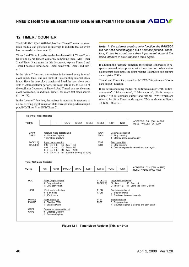
HMS81C1404B/08B/16B/1508B/1516B/1608B/1616B/1708B/1716B/1808B/1816B
12. TIMER / COUNTERThe HMS81C1X04B/08B/16B has four Timer/Counter registers.Each module can generate an interrupt to indicate that an eventhas occurred (i.e. timer match).
Timer 0 and Timer 1 can be used either the two 8-bit Timer/Coun-ter or one 16-bit Timer/Counter by combining them. Also Timer2 and Timer 3 are same. In this document, explain Timer 0 andTimer 1 because Timer2 and Timer3 same with Timer 0 and Tim-er 1.
In the “timer” function, the register is increased every internalclock input. Thus, one can think of it as counting internal clockinput. Since the least clock consists of 2 and the most clock con-sists of 2048 oscillator periods, the count rate is 1/2 to 1/2048 ofthe oscillator frequency in Timer0. And Timer1 can use the sameclock source too. In addition, Timer1 has more fast clock source(1/1 to 1/8).
In the “counter” function, the register is increased in response toa 0-to-1 (rising edge) transition at its corresponding external inputpin, EC0(Timer 0) or EC1(Timer 2).
Note: In the external event counter function, the RA0/EC0pin has not a schmitt trigger, but a normal input port. There-fore, it may be count more than input event signal if thenoise interfere in slow transition input signal.
In addition the “capture” function, the register is increased in re-sponse external interrupt same with timer function. When exter-nal interrupt edge input, the count register is captured into capturedata register CDRx.
Timer1 and Timer 3 are shared with “PWM” function and “Com-pare output” function
It has seven operating modes: “8-bit timer/counter”, “16-bit tim-er/counter”, “8-bit capture”, “16-bit capture”, “8-bit compareoutput”, “16-bit compare output” and “10-bit PWM” which areselected by bit in Timer mode register TMx as shown in Figure12-1and Table 12-1.
Figure 12-1 Timer Mode Register (TMx, x = 0~3)
Timer 0(2) Mode Register
TM0(2)ADDRESS : D0H (D6H for TM2)RESET VALUE : --00_0000- - CAPx TxCK2 TxCK1 TxCK0 TxCN TxST
Timer 1(3) Mode Register
TM1(3)ADDRESS : D2H (D8H for TM3)RESET VALUE : 0000_0000POL 16BIT PWMxE CAPx TxCK1 TxCK0 TxCN TxST
CAP0CAP2
Capture mode selection bit.0 : Disables Capture1 : Enables Capture
T0CNT2CN
Continue control bit0 : Stop counting1 : Start counting continuously
T0CK[2:0]T2CK[2:0]
Input clock selection000 : fxin ÷ 2, 100 : fxin ÷ 128001 : fxin ÷ 4, 101 : fxin ÷ 512010 : fxin ÷ 8, 110 : fxin ÷ 2048011 : fxin ÷ 32, 111 : External Event ( EC0(1) )
T0STT2ST
Start control bit0 : Stop counting1 : Counter register is cleared and start again
POL PWM Output Polarity0 : Duty active low1 : Duty active high
T1CK[2:0]T3CK[2:0]
Input clock selection00 : fxin 10 : fxin ÷ 801 : fxin ÷ 2 11 : using the Timer 0 clock
16BIT 16-bit mode selection0 : 8-bit mode1 : 16-bit mode
T1CNT3CN
Continue control bit0 : Stop counting1 : Start counting continuously
PWM0EPWM1E
PWM enable bit0 : Disables PWM1 : Enables PWM
T1STT3ST
Start control bit0 : Stop counting1 : Counter register is cleared and start again
CAP1CAP3
Capture mode selection bit.0 : Disables Capture1 : Enables Capture
46 April 2, 2008 Ver 1.20
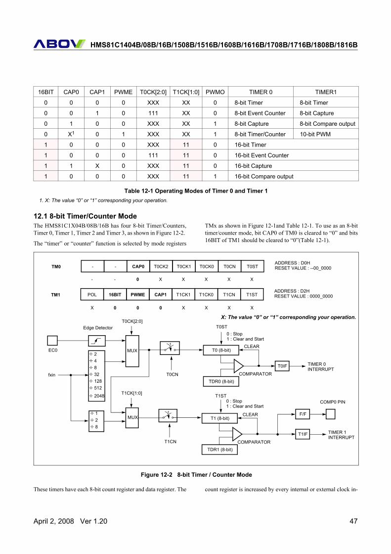
HMS81C1404B/08B/16B/1508B/1516B/1608B/1616B/1708B/1716B/1808B/1816B
12.1 8-bit Timer/Counter ModeThe HMS81C1X04B/08B/16B has four 8-bit Timer/Counters,Timer 0, Timer 1, Timer 2 and Timer 3, as shown in Figure 12-2.
The “timer” or “counter” function is selected by mode registers
TMx as shown in Figure 12-1and Table 12-1. To use as an 8-bittimer/counter mode, bit CAP0 of TM0 is cleared to “0” and bits16BIT of TM1 should be cleared to “0”(Table 12-1).
Figure 12-2 8-bit Timer / Counter Mode
These timers have each 8-bit count register and data register. The count register is increased by every internal or external clock in-
16BIT CAP0 CAP1 PWME T0CK[2:0] T1CK[1:0] PWMO TIMER 0 TIMER1
0 0 0 0 XXX XX 0 8-bit Timer 8-bit Timer
0 0 1 0 111 XX 0 8-bit Event Counter 8-bit Capture
0 1 0 0 XXX XX 1 8-bit Capture 8-bit Compare output
0 X1 0 1 XXX XX 1 8-bit Timer/Counter 10-bit PWM
1 0 0 0 XXX 11 0 16-bit Timer
1 0 0 0 111 11 0 16-bit Event Counter
1 1 X 0 XXX 11 0 16-bit Capture
1 0 0 0 XXX 11 1 16-bit Compare output
Table 12-1 Operating Modes of Timer 0 and Timer 11. X: The value “0” or “1” corresponding your operation.
÷ 1÷ 2÷ 8
TM0ADDRESS : D0HRESET VALUE : --00_0000- - CAP0 T0CK2 T0CK1 T0CK0 T0CN T0ST
TM1ADDRESS : D2HRESET VALUE : 0000_0000POL 16BIT PWME CAP1 T1CK1 T1CK0 T1CN T1ST
- - 0 X X X X X
X 0 0 0 X X X X
÷ 2÷ 4
÷ 128÷ 512
÷ 8÷ 32fxin
EC0
Edge Detector
MUX
MUX
1
1
T0 (8-bit)
TDR0 (8-bit)
T0IF
CLEAR
COMPARATOR
TIMER 0INTERRUPT
T1 (8-bit)
TDR1 (8-bit)
T1IF
CLEAR
COMPARATOR
TIMER 1INTERRUPT
T0ST0 : Stop1 : Clear and Start
T1ST0 : Stop1 : Clear and Start
T0CN
T1CN
T0CK[2:0]
T1CK[1:0]
F/F
COMP0 PIN÷ 2048
X: The value “0” or “1” corresponding your operation.
April 2, 2008 Ver 1.20 47
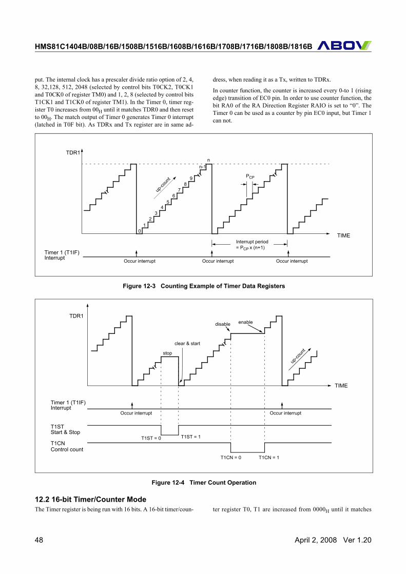
HMS81C1404B/08B/16B/1508B/1516B/1608B/1616B/1708B/1716B/1808B/1816B
put. The internal clock has a prescaler divide ratio option of 2, 4,8, 32,128, 512, 2048 (selected by control bits T0CK2, T0CK1and T0CK0 of register TM0) and 1, 2, 8 (selected by control bitsT1CK1 and T1CK0 of register TM1). In the Timer 0, timer reg-ister T0 increases from 00H until it matches TDR0 and then resetto 00H. The match output of Timer 0 generates Timer 0 interrupt(latched in T0F bit). As TDRx and Tx register are in same ad-
dress, when reading it as a Tx, written to TDRx.
In counter function, the counter is increased every 0-to 1 (risingedge) transition of EC0 pin. In order to use counter function, thebit RA0 of the RA Direction Register RAIO is set to “0”. TheTimer 0 can be used as a counter by pin EC0 input, but Timer 1can not.
Figure 12-3 Counting Example of Timer Data Registers
Figure 12-4 Timer Count Operation
12.2 16-bit Timer/Counter ModeThe Timer register is being run with 16 bits. A 16-bit timer/coun- ter register T0, T1 are increased from 0000H until it matches
~~
Timer 1 (T1IF)Interrupt
TDR1
TIME
Occur interrupt Occur interrupt Occur interrupt
Interrupt period
up-co
unt
~~ ~~
01
23
45
67
89
nn-1
PCP
= PCP x (n+1)
Timer 1 (T1IF)Interrupt
TDR1
TIME
Occur interrupt Occur interrupt
stop
clear & start
disable enable
Start & StopT1ST
T1CNControl count
up-co
unt
~~
~~
T1ST = 0 T1ST = 1
T1CN = 0 T1CN = 1
48 April 2, 2008 Ver 1.20
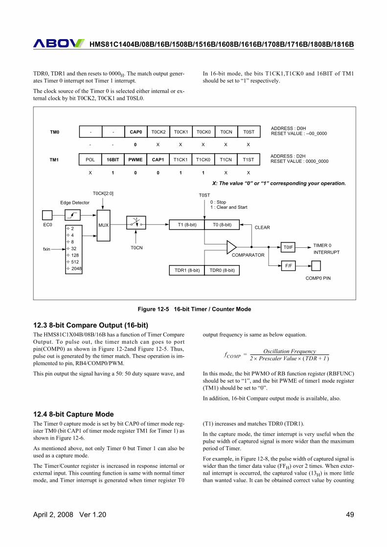
HMS81C1404B/08B/16B/1508B/1516B/1608B/1616B/1708B/1716B/1808B/1816B
TDR0, TDR1 and then resets to 0000H. The match output gener-ates Timer 0 interrupt not Timer 1 interrupt.
The clock source of the Timer 0 is selected either internal or ex-ternal clock by bit T0CK2, T0CK1 and T0SL0.
In 16-bit mode, the bits T1CK1,T1CK0 and 16BIT of TM1should be set to “1” respectively.
Figure 12-5 16-bit Timer / Counter Mode
12.3 8-bit Compare Output (16-bit)The HMS81C1X04B/08B/16B has a function of Timer CompareOutput. To pulse out, the timer match can goes to portpin(COMP0) as shown in Figure 12-2and Figure 12-5. Thus,pulse out is generated by the timer match. These operation is im-plemented to pin, RB4/COMP0/PWM.
This pin output the signal having a 50: 50 duty square wave, and
output frequency is same as below equation.
In this mode, the bit PWMO of RB function register (RBFUNC)should be set to “1”, and the bit PWME of timer1 mode register(TM1) should be set to “0”.
In addition, 16-bit Compare output mode is available, also.
12.4 8-bit Capture ModeThe Timer 0 capture mode is set by bit CAP0 of timer mode reg-ister TM0 (bit CAP1 of timer mode register TM1 for Timer 1) asshown in Figure 12-6.
As mentioned above, not only Timer 0 but Timer 1 can also beused as a capture mode.
The Timer/Counter register is increased in response internal orexternal input. This counting function is same with normal timermode, and Timer interrupt is generated when timer register T0
(T1) increases and matches TDR0 (TDR1).
In the capture mode, the timer interrupt is very useful when thepulse width of captured signal is more wider than the maximumperiod of Timer.
For example, in Figure 12-8, the pulse width of captured signal iswider than the timer data value (FFH) over 2 times. When exter-nal interrupt is occurred, the captured value (13H) is more littlethan wanted value. It can be obtained correct value by counting
TM0ADDRESS : D0HRESET VALUE : --00_0000- - CAP0 T0CK2 T0CK1 T0CK0 T0CN T0ST
TM1ADDRESS : D2HRESET VALUE : 0000_0000POL 16BIT PWME CAP1 T1CK1 T1CK0 T1CN T1ST
- - 0 X X X X X
X 1 0 0 1 1 X X
÷ 2÷ 4
÷ 128÷ 512
÷ 8÷ 32fxin
EC0
Edge Detector
MUX1
T1 (8-bit)
TDR1 (8-bit)
T0IF
CLEAR
COMPARATOR
TIMER 0INTERRUPT
T0 (8-bit)
TDR0 (8-bit)
T0ST0 : Stop1 : Clear and Start
T0CN
T0CK[2:0]
F/F
COMP0 PIN
÷ 2048
X: The value “0” or “1” corresponding your operation.
fCOMPOscillation Frequency
2 Prescaler Value TDR 1 )+(××---------------------------------------------------------------------------------=
April 2, 2008 Ver 1.20 49
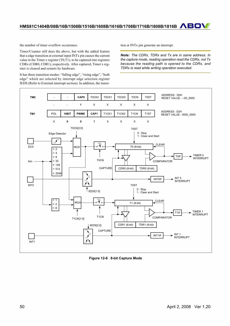
HMS81C1404B/08B/16B/1508B/1516B/1608B/1616B/1708B/1716B/1808B/1816B
the number of timer overflow occurrence.
Timer/Counter still does the above, but with the added featurethat a edge transition at external input INTx pin causes the currentvalue in the Timer x register (T0,T1), to be captured into registersCDRx (CDR0, CDR1), respectively. After captured, Timer x reg-ister is cleared and restarts by hardware.
It has three transition modes: “falling edge”, “rising edge”, “bothedge” which are selected by interrupt edge selection registerIEDS (Refer to External interrupt section). In addition, the transi-
tion at INTx pin generate an interrupt.
Note: The CDRx, TDRx and Tx are in same address. Inthe capture mode, reading operation read the CDRx, not Txbecause the reading path is opened to the CDRx, andTDRx is read while writing operation executed.
Figure 12-6 8-bit Capture Mode
÷ 1÷ 2÷ 8
TM0ADDRESS : D0HRESET VALUE : --00_0000- - CAP0 T0CK2 T0CK1 T0CK0 T0CN T0ST
TM1ADDRESS : D2HRESET VALUE : 0000_0000POL 16BIT PWME CAP1 T1CK1 T1CK0 T1CN T1ST
- - 1 X X X X X
X 0 0 1 X X X X
÷ 2÷ 4
÷ 128÷ 512
÷ 8÷ 32fxin
EC0
Edge Detector
MUX
MUX
1
1
T0 (8-bit)
CDR0 (8-bit)
T0IF
CLEAR
COMPARATOR
TIMER 0INTERRUPT
T0ST0 : Stop1 : Clear and Start
T0CN
T1CN
T0CK[2:0]
T1CK[1:0]
TDR0 (8-bit)
INT0IF INT 0INTERRUPT
INT0
T1 (8-bit)
CDR1 (8-bit)
T1IF
CLEAR
COMPARATOR
TIMER 1INTERRUPT
TDR1 (8-bit)
INT1IF INT 1INTERRUPT
INT1
T0ST0 : Stop1 : Clear and StartIEDS[1:0]
IEDS[3:2]
CAPTURE
CAPTURE
÷ 2048
50 April 2, 2008 Ver 1.20
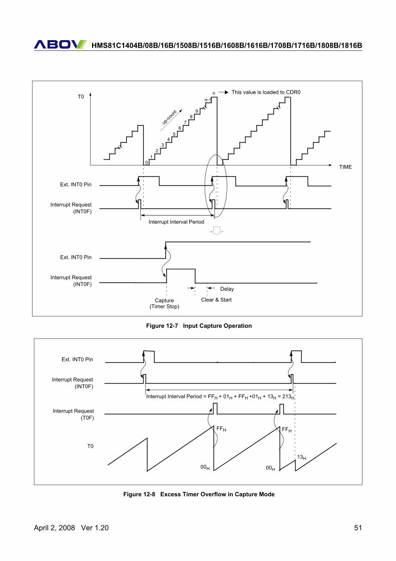
HMS81C1404B/08B/16B/1508B/1516B/1608B/1616B/1708B/1716B/1808B/1816B
Figure 12-7 Input Capture Operation
Figure 12-8 Excess Timer Overflow in Capture Mode
~~
Ext. INT0 Pin
Interrupt Request
T0
TIME
up-co
unt
~~ ~~
01
23
45
67
89
nn-1
Capture(Timer Stop)
Clear & Start
Interrupt Interval Period
Delay
(INT0F)
Ext. INT0 Pin
Interrupt Request(INT0F)
This value is loaded to CDR0
Interrupt Interval Period = FFH + 01H + FFH +01H + 13H = 213H
FFH FFH
Ext. INT0 Pin
Interrupt Request(INT0F)
00H 00H
Interrupt Request(T0F)
T0
13H
April 2, 2008 Ver 1.20 51
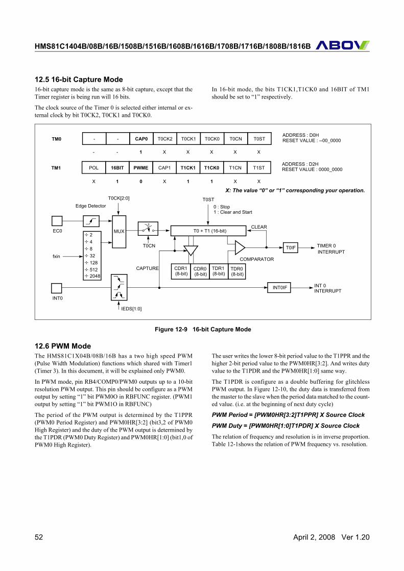
HMS81C1404B/08B/16B/1508B/1516B/1608B/1616B/1708B/1716B/1808B/1816B
12.5 16-bit Capture Mode16-bit capture mode is the same as 8-bit capture, except that theTimer register is being run will 16 bits.
The clock source of the Timer 0 is selected either internal or ex-ternal clock by bit T0CK2, T0CK1 and T0CK0.
In 16-bit mode, the bits T1CK1,T1CK0 and 16BIT of TM1should be set to “1” respectively.
Figure 12-9 16-bit Capture Mode
12.6 PWM ModeThe HMS81C1X04B/08B/16B has a two high speed PWM(Pulse Width Modulation) functions which shared with Timer1(Timer 3). In this document, it will be explained only PWM0.
In PWM mode, pin RB4/COMP0/PWM0 outputs up to a 10-bitresolution PWM output. This pin should be configure as a PWMoutput by setting “1” bit PWM0O in RBFUNC register. (PWM1output by setting “1” bit PWM1O in RBFUNC)
The period of the PWM output is determined by the T1PPR(PWM0 Period Register) and PWM0HR[3:2] (bit3,2 of PWM0High Register) and the duty of the PWM output is determined bythe T1PDR (PWM0 Duty Register) and PWM0HR[1:0] (bit1,0 ofPWM0 High Register).
The user writes the lower 8-bit period value to the T1PPR and thehigher 2-bit period value to the PWM0HR[3:2]. And writes dutyvalue to the T1PDR and the PWM0HR[1:0] same way.
The T1PDR is configure as a double buffering for glitchlessPWM output. In Figure 12-10, the duty data is transferred fromthe master to the slave when the period data matched to the count-ed value. (i.e. at the beginning of next duty cycle)
PWM Period = [PWM0HR[3:2]T1PPR] X Source Clock
PWM Duty = [PWM0HR[1:0]T1PDR] X Source Clock
The relation of frequency and resolution is in inverse proportion.Table 12-1shows the relation of PWM frequency vs. resolution.
TM0ADDRESS : D0HRESET VALUE : --00_0000- - CAP0 T0CK2 T0CK1 T0CK0 T0CN T0ST
TM1ADDRESS : D2HRESET VALUE : 0000_0000POL 16BIT PWME CAP1 T1CK1 T1CK0 T1CN T1ST
- - 1 X X X X X
X 1 0 X 1 1 X X
÷ 2÷ 4
÷ 128÷ 512
÷ 8÷ 32fxin
EC0
Edge Detector
MUX1
T0 + T1 (16-bit)
TDR1
T0IF
CLEAR
COMPARATOR
TIMER 0INTERRUPT
T0ST0 : Stop1 : Clear and Start
T0CN
T0CK[2:0]
TDR0
INT0IF INT 0INTERRUPT
INT0
IEDS[1:0]
CAPTURE CDR1 CDR0 (8-bit) (8-bit) (8-bit) (8-bit)÷ 2048
X: The value “0” or “1” corresponding your operation.
52 April 2, 2008 Ver 1.20
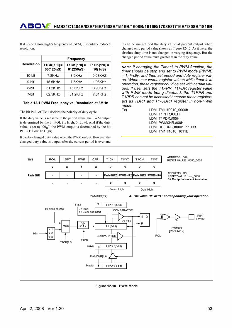
HMS81C1404B/08B/16B/1508B/1516B/1608B/1616B/1708B/1716B/1808B/1816B
If it needed more higher frequency of PWM, it should be reducedresolution.
The bit POL of TM1 decides the polarity of duty cycle.
If the duty value is set same to the period value, the PWM outputis determined by the bit POL (1: High, 0: Low). And if the dutyvalue is set to “00H”, the PWM output is determined by the bitPOL (1: Low, 0: High).
It can be changed duty value when the PWM output. However thechanged duty value is output after the current period is over and
it can be maintained the duty value at present output whenchanged only period value shown as Figure 12-12. As it were, theabsolute duty time is not changed in varying frequency. But thechanged period value must greater than the duty value.
Note: If changing the Timer1 to PWM function, thetimer should be stop and set to PWM mode (PWME= 1) firstly, and then set period and duty register val-ue. When user writes register values while timer is inoperation, these register could be set with certain val-ues. If user sets the T1PPR, T1PDR register valuewith PWM mode being disabled, the T1PPR andT1PDR can not be accessed because these registersact as TDR1 and T1/CDR1 register in non-PWMmode. Ex) LDM TM1,#0010_0000b
LDM T1PPR,#0EHLDM T1PDR,#05HLDM PWM0HR,#00HLDM RBFUNC,#0001_1100BLDM TM1,#1010_1011B
Figure 12-10 PWM Mode
ResolutionFrequency
T1CK[1:0] = 00(125nS)
T1CK[1:0] = 01(250nS)
T1CK[1:0] = 10(1uS)
10-bit 7.8KHz 3.9KHz 0.98KHZ
9-bit 15.6KHz 7.8KHz 1.95KHz
8-bit 31.2KHz 15.6KHz 3.90KHz
7-bit 62.5KHz 31.2KHz 7.81KHz
Table 12-1 PWM Frequency vs. Resolution at 8MHz
÷ 1÷ 2÷ 8
PWM0HRADDRESS : D5HRESET VALUE : ----_0000- - - - PWM0HR3 PWM0HR2 PWM0HR1 PWM0HR0
- - - - X X X X
MUX1
T1CNT1CK[1:0]
T1 (8-bit)
T1ST0 : Stop1 : Clear and Start
CLEAR
COMPARATOR
COMPARATOR
T1PDR(8-bit)
PWM0HR[1:0]
T1PPR(8-bit)
PWM0HR[3:2]
T1PDR(8-bit)
S Q
R
POL
PWM0O
RB4/PWM0
T0 clock source
fxin
TM1ADDRESS : D2HRESET VALUE : 0000_0000POL 16BIT PWME CAP1 T1CK1 T1CK0 T1CN T1ST
X 0 1 0 X X X X
[RBFUNC.4]
Period High Duty High
Slave
Master
Bit Manipulation Not Available
X: The value “0” or “1” corresponding your operation.
April 2, 2008 Ver 1.20 53
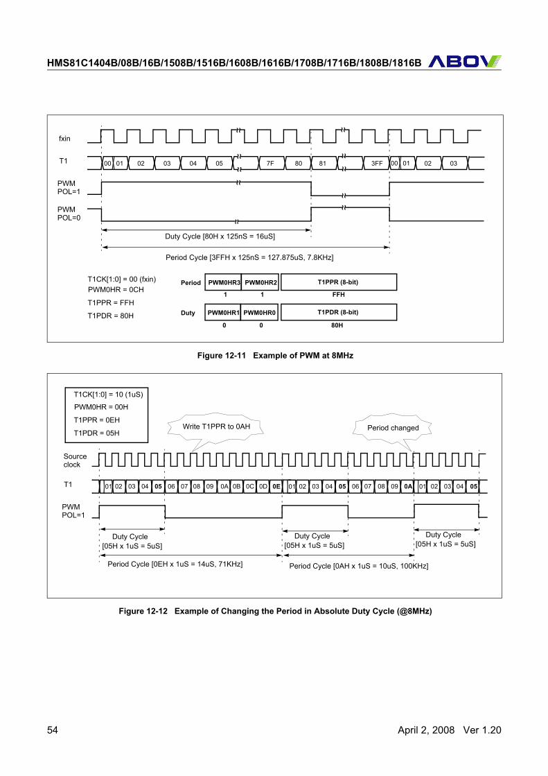
HMS81C1404B/08B/16B/1508B/1516B/1608B/1616B/1708B/1716B/1808B/1816B
Figure 12-11 Example of PWM at 8MHz
Figure 12-12 Example of Changing the Period in Absolute Duty Cycle (@8MHz)
fxin
T1
PWM
~~~~
~~
01 02 03 04 05 7F 80 81 3FF 02 03
~~~~
~~
~~
~~
~~
~~
POL=1
PWMPOL=0
Duty Cycle [80H x 125nS = 16uS]
Period Cycle [3FFH x 125nS = 127.875uS, 7.8KHz]
PWM0HR = 0CH
T1PPR = FFH
T1PDR = 80H
T1CK[1:0] = 00 (fxin) PWM0HR3 PWM0HR2
PWM0HR1 PWM0HR0
T1PPR (8-bit)
T1PDR (8-bit)
Period
Duty
1 1 FFH
0 0 80H
00 0100
Source
T1
PWMPOL=1
Duty Cycle
Period Cycle [0EH x 1uS = 14uS, 71KHz]
PWM0HR = 00H
T1PPR = 0EH
T1PDR = 05H
T1CK[1:0] = 10 (1uS)
01 02 03 04 05 06 08 09 0B 0C 0D 0E 01 02 03 04 05 06 07 08 09 0A 01 02 03 0407 0A 05
[05H x 1uS = 5uS]Duty Cycle
[05H x 1uS = 5uS]
Period Cycle [0AH x 1uS = 10uS, 100KHz]
Duty Cycle [05H x 1uS = 5uS]
Write T1PPR to 0AH Period changed
clock
54 April 2, 2008 Ver 1.20
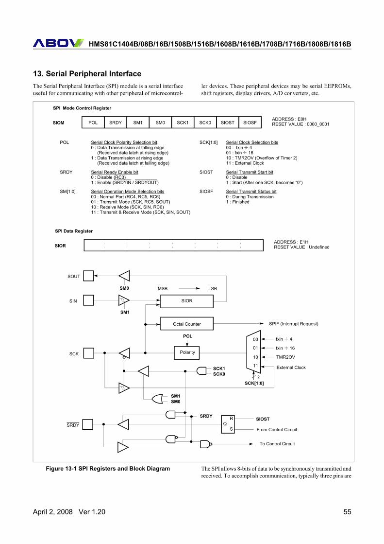
HMS81C1404B/08B/16B/1508B/1516B/1608B/1616B/1708B/1716B/1808B/1816B
13. Serial Peripheral InterfaceThe Serial Peripheral Interface (SPI) module is a serial interfaceuseful for communicating with other peripheral of microcontrol-
ler devices. These peripheral devices may be serial EEPROMs,shift registers, display drivers, A/D converters, etc.
Figure 13-1 SPI Registers and Block Diagram The SPI allows 8-bits of data to be synchronously transmitted andreceived. To accomplish communication, typically three pins are
External Clock
SCK[1:0]
MSB LSB
SOUT
SIN
SCK Polarity
SIOR
fxin ÷ 4fxin ÷ 16
TMR2OV
SCK1SCK0
SM1SM0
SRDY
SM1
SM0
POL
Octal Counter
2
SPIF (Interrupt Request)
SRDYQ
R
S
SIOST
From Control Circuit
To Control Circuit
SPI Mode Control Register
SIOMADDRESS : E0HRESET VALUE : 0000_0001POL SRDY SM1 SM0 SCK1 SCK0 SIOST SIOSF
POL Serial Clock Polarity Selection bit.0 : Data Transmission at falling edge (Received data latch at rising edge)1 : Data Transmission at rising edge (Received data latch at falling edge)
SCK[1:0] Serial Clock Selection bits00 : fxin ÷ 401 : fxin ÷ 1610 : TMR2OV (Overflow of Timer 2)11 : External Clock
SRDY Serial Ready Enable bit0 : Disable (RC3)1 : Enable (SRDYIN / SRDYOUT)
SIOST Serial Transmit Start bit0 : Disable1 : Start (After one SCK, becomes “0”)
SM[1:0] Serial Operation Mode Selection bits00 : Normal Port (RC4, RC5, RC6)01 : Transmit Mode (SCK, RC5, SOUT)10 : Receive Mode (SCK, SIN, RC6)11 : Transmit & Receive Mode (SCK, SIN, SOUT)
SIOSF Serial Transmit Status bit0 : During Transmission1 : Finished
SPI Data Register
SIORADDRESS : E1H RESET VALUE : Undefined
00
01
10
11
April 2, 2008 Ver 1.20 55
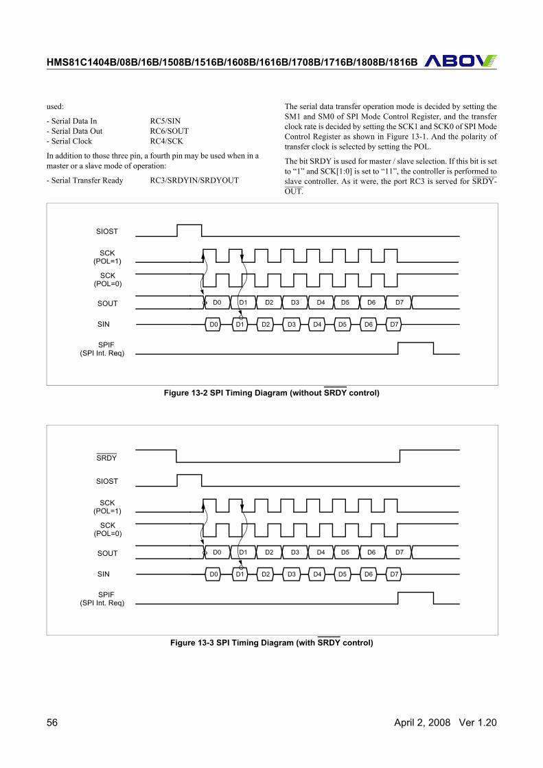
HMS81C1404B/08B/16B/1508B/1516B/1608B/1616B/1708B/1716B/1808B/1816B
used:
- Serial Data In RC5/SIN- Serial Data Out RC6/SOUT- Serial Clock RC4/SCK
In addition to those three pin, a fourth pin may be used when in amaster or a slave mode of operation:
- Serial Transfer Ready RC3/SRDYIN/SRDYOUT
The serial data transfer operation mode is decided by setting theSM1 and SM0 of SPI Mode Control Register, and the transferclock rate is decided by setting the SCK1 and SCK0 of SPI ModeControl Register as shown in Figure 13-1. And the polarity oftransfer clock is selected by setting the POL.
The bit SRDY is used for master / slave selection. If this bit is setto “1” and SCK[1:0] is set to “11”, the controller is performed toslave controller. As it were, the port RC3 is served for SRDY-OUT.
Figure 13-2 SPI Timing Diagram (without SRDY control)
Figure 13-3 SPI Timing Diagram (with SRDY control)
D1 D2 D3 D4 D6 D7D0 D5
D1 D2 D3 D4 D6 D7D0 D5
SIOST
SCK(POL=1)
SCK(POL=0)
SOUT
SIN
SPIF(SPI Int. Req)
D1 D2 D3 D4 D6 D7D0 D5
D1 D2 D3 D4 D6 D7D0 D5
SRDY
SIOST
SCK(POL=1)
SCK(POL=0)
SOUT
SIN
SPIF(SPI Int. Req)
56 April 2, 2008 Ver 1.20
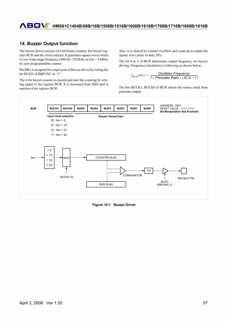
HMS81C1404B/08B/16B/1508B/1516B/1608B/1616B/1708B/1716B/1808B/1816B
14. Buzzer Output functionThe buzzer driver consists of 6-bit binary counter, the buzzer reg-ister BUR and the clock selector. It generates square-wave whichis very wide range frequency (480 Hz~250 KHz at fxin = 4 MHz)by user programmable counter.
Pin RB1 is assigned for output port of Buzzer driver by setting thebit BUZO of RBFUNC to “1”.
The 6-bit buzzer counter is cleared and start the counting by writ-ing signal to the register BUR. It is increased from 00H until itmatches 6-bit register BUR.
Also, it is cleared by counter overflow and count up to output thesquare wave pulse of duty 50%.
The bit 0 to 5 of BUR determines output frequency for buzzerdriving. Frequency calculation is following as shown below.
The bits BUCK1, BUCK0 of BUR selects the source clock fromprescaler output.
Figure 14-1 Buzzer Driver
fBUZ Hz( ) Oscillator Frequency2 Prescaler Ratio BUR 1+( )××-----------------------------------------------------------------------------------=
BURADDRESS : DEHRESET VALUE : 1111_1111BUCK1 BUCK0 BUR5 BUR4 BUR3 BUR2 BUR1 BUR0
÷ 64
÷ 16
÷ 32fxin MUX COUNTER (6-bit)
BUR (6-bit)
F/F
COMPARATORBUCK[1:0] RB1/BUZ PIN
÷ 8
Input clock selection00 : fxin ÷ 8
01 : fxin ÷ 16
10 : fxin ÷ 32
11 : fxin ÷ 64
Buzzer Period Data
BUZO[RBFUNC.1]
Bit Manipulation Not Available
April 2, 2008 Ver 1.20 57
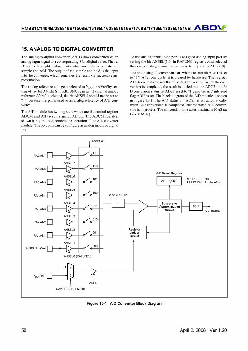
HMS81C1404B/08B/16B/1508B/1516B/1608B/1616B/1708B/1716B/1808B/1816B
15. ANALOG TO DIGITAL CONVERTERThe analog-to-digital converter (A/D) allows conversion of ananalog input signal to a corresponding 8-bit digital value. The A/D module has eight analog inputs, which are multiplexed into onesample and hold. The output of the sample and hold is the inputinto the converter, which generates the result via successive ap-proximation.
The analog reference voltage is selected to VDD or AVref by set-ting of the bit AVREFS in RBFUNC register. If external analogreference AVref is selected, the bit ANSEL0 should not be set to“1”, because this pin is used to an analog reference of A/D con-verter.
The A/D module has two registers which are the control registerADCM and A/D result register ADCR. The ADCM register,shown in Figure 15-2, controls the operation of the A/D convertermodule. The port pins can be configure as analog inputs or digitalI/O.
To use analog inputs, each port is assigned analog input port bysetting the bit ANSEL[7:0] in RAFUNC register. And selectedthe corresponding channel to be converted by setting ADS[2:0].
The processing of conversion start when the start bit ADST is setto “1”. After one cycle, it is cleared by hardware. The registerADCR contains the results of the A/D conversion. When the con-version is completed, the result is loaded into the ADCR, the A/D conversion status bit ADSF is set to “1”, and the A/D interruptflag ADIF is set. The block diagram of the A/D module is shownin Figure 15-1. The A/D status bit, ADSF is set automaticallywhen A/D conversion is completed, cleared when A/D conver-sion is in process. The conversion time takes maximum 10 uS (atfxin=8 MHz).
Figure 15-1 A/D Converter Block Diagram
RB0/AN0/AVref
ANSEL0 (RAFUNC.0)
RA1/AN1
ANSEL1
RA2/AN2
ANSEL2
RA3/AN3
ANSEL3
RA4/AN4
ANSEL4
RA5/AN5
ANSEL5
RA6/AN6
ANSEL6
RA7/AN7
ANSEL7
000
001
010
011
100
101
110
111
VDD Pin
1
0
AVREFS (RBFUNC.0)
ADEN
S/H SuccessiveApproximation
Circuit ADIF
ResistorLadderCircuit
ADS[2:0]
ADCR(8-bit)
Sample & Hold
A/D Interrupt
ADDRESS : EBHRESET VALUE : Undefined
A/D Result Register
58 April 2, 2008 Ver 1.20
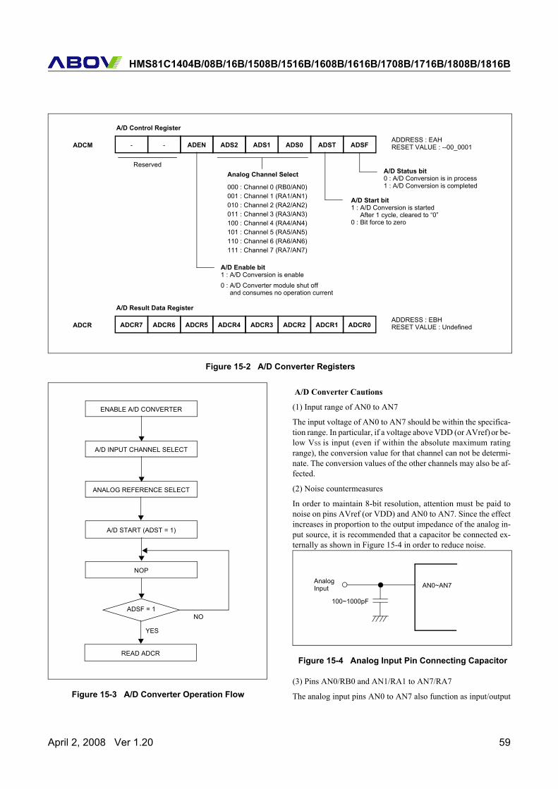
HMS81C1404B/08B/16B/1508B/1516B/1608B/1616B/1708B/1716B/1808B/1816B
Figure 15-2 A/D Converter Registers
Figure 15-3 A/D Converter Operation Flow
A/D Converter Cautions
(1) Input range of AN0 to AN7
The input voltage of AN0 to AN7 should be within the specifica-tion range. In particular, if a voltage above VDD (or AVref) or be-low VSS is input (even if within the absolute maximum ratingrange), the conversion value for that channel can not be determi-nate. The conversion values of the other channels may also be af-fected.
(2) Noise countermeasures
In order to maintain 8-bit resolution, attention must be paid tonoise on pins AVref (or VDD) and AN0 to AN7. Since the effectincreases in proportion to the output impedance of the analog in-put source, it is recommended that a capacitor be connected ex-ternally as shown in Figure 15-4 in order to reduce noise.
Figure 15-4 Analog Input Pin Connecting Capacitor
(3) Pins AN0/RB0 and AN1/RA1 to AN7/RA7
The analog input pins AN0 to AN7 also function as input/output
ADCMADDRESS : EAHRESET VALUE : --00_0001- - ADEN ADS2 ADS1 ADS0 ADST ADSF
ReservedAnalog Channel Select A/D Status bit
0 : A/D Conversion is in process1 : A/D Conversion is completed
A/D Start bit1 : A/D Conversion is started After 1 cycle, cleared to “0”0 : Bit force to zero
000 : Channel 0 (RB0/AN0)001 : Channel 1 (RA1/AN1)010 : Channel 2 (RA2/AN2)011 : Channel 3 (RA3/AN3)100 : Channel 4 (RA4/AN4)101 : Channel 5 (RA5/AN5)110 : Channel 6 (RA6/AN6)111 : Channel 7 (RA7/AN7)
A/D Enable bit1 : A/D Conversion is enable0 : A/D Converter module shut off and consumes no operation current
A/D Control Register
ADCRADDRESS : EBHRESET VALUE : UndefinedADCR7 ADCR6 ADCR5 ADCR4 ADCR3 ADCR2 ADCR1 ADCR0
A/D Result Data Register
ENABLE A/D CONVERTER
A/D START (ADST = 1)
NOP
ADSF = 1
A/D INPUT CHANNEL SELECT
ANALOG REFERENCE SELECT
READ ADCR
YES
NO
AN0~AN7
100~1000pF
AnalogInput
April 2, 2008 Ver 1.20 59

HMS81C1404B/08B/16B/1508B/1516B/1608B/1616B/1708B/1716B/1808B/1816B
port (PORT RA and RB0) pins. When A/D conversion is per-formed with any of pins AN0 to AN7 selected, be sure not to ex-ecute a PORT input instruction while conversion is in progress,as this may reduce the conversion resolution.
Also, if digital pulses are applied to a pin adjacent to the pin in theprocess of A/D conversion, the expected A/D conversion valuemay not be obtainable due to coupling noise. Therefore, avoid ap-plying pulses to pins adjacent to the pin undergoing A/D conver-sion.
(4) AVref pin input impedance
A series resistor string of approximately 10KΩ is connected be-tween the AVref pin and the VSS pin.
Therefore, if the output impedance of the reference voltagesource is high, this will result in parallel connection to the seriesresistor string between the AVref pin and the VSS pin, and therewill be a large reference voltage error.
60 April 2, 2008 Ver 1.20
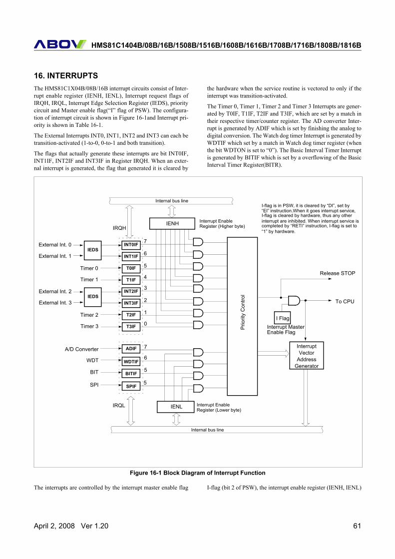
HMS81C1404B/08B/16B/1508B/1516B/1608B/1616B/1708B/1716B/1808B/1816B
16. INTERRUPTSThe HMS81C1X04B/08B/16B interrupt circuits consist of Inter-rupt enable register (IENH, IENL), Interrupt request flags ofIRQH, IRQL, Interrupt Edge Selection Register (IEDS), prioritycircuit and Master enable flag(“I” flag of PSW). The configura-tion of interrupt circuit is shown in Figure 16-1and Interrupt pri-ority is shown in Table 16-1.
The External Interrupts INT0, INT1, INT2 and INT3 can each betransition-activated (1-to-0, 0-to-1 and both transition).
The flags that actually generate these interrupts are bit INT0IF,INT1IF, INT2IF and INT3IF in Register IRQH. When an exter-nal interrupt is generated, the flag that generated it is cleared by
the hardware when the service routine is vectored to only if theinterrupt was transition-activated.
The Timer 0, Timer 1, Timer 2 and Timer 3 Interrupts are gener-ated by T0IF, T1IF, T2IF and T3IF, which are set by a match intheir respective timer/counter register. The AD converter Inter-rupt is generated by ADIF which is set by finishing the analog todigital conversion. The Watch dog timer Interrupt is generated byWDTIF which set by a match in Watch dog timer register (whenthe bit WDTON is set to “0”). The Basic Interval Timer Interruptis generated by BITIF which is set by a overflowing of the BasicInterval Timer Register(BITR).
Figure 16-1 Block Diagram of Interrupt Function
The interrupts are controlled by the interrupt master enable flag I-flag (bit 2 of PSW), the interrupt enable register (IENH, IENL)
BIT BITIF
WDTIFWDT
A/D Converter
Timer 1
Timer 0
External Int. 1
External Int. 0
IENH Interrupt Enable
Interrupt Enable
IRQH
IRQL
InterruptVector
AddressGenerator
Internal bus line
Register (Lower byte)
Internal bus line
Register (Higher byte)
Release STOP
To CPU
Interrupt MasterEnable Flag
I Flag
IENL
Prio
rity
Con
trol
I-flag is in PSW, it is cleared by “DI”, set by“EI” instruction.When it goes interrupt service,I-flag is cleared by hardware, thus any otherinterrupt are inhibited. When interrupt service iscompleted by “RETI” instruction, I-flag is set to“1” by hardware.
INT0IF
INT1IF
T0IF
T1IF
ADIF
7
6
5
4
7
6
5
IEDS
Timer 3
Timer 2
External Int. 3
External Int. 2 INT2IF
INT3IF
T2IF
T3IF
3
2
1
0
IEDS
SPI SPIF5
April 2, 2008 Ver 1.20 61
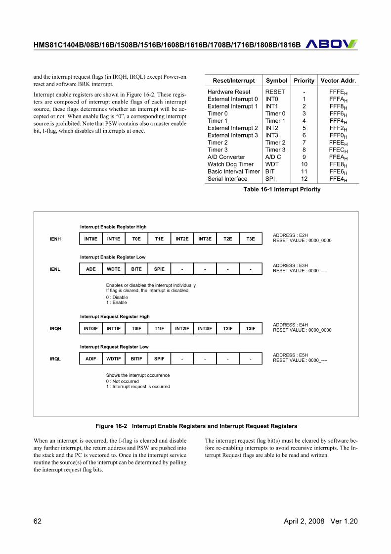
HMS81C1404B/08B/16B/1508B/1516B/1608B/1616B/1708B/1716B/1808B/1816B
and the interrupt request flags (in IRQH, IRQL) except Power-onreset and software BRK interrupt.
Interrupt enable registers are shown in Figure 16-2. These regis-ters are composed of interrupt enable flags of each interruptsource, these flags determines whether an interrupt will be ac-cepted or not. When enable flag is “0”, a corresponding interruptsource is prohibited. Note that PSW contains also a master enablebit, I-flag, which disables all interrupts at once.
Figure 16-2 Interrupt Enable Registers and Interrupt Request Registers
When an interrupt is occurred, the I-flag is cleared and disableany further interrupt, the return address and PSW are pushed intothe stack and the PC is vectored to. Once in the interrupt serviceroutine the source(s) of the interrupt can be determined by pollingthe interrupt request flag bits.
The interrupt request flag bit(s) must be cleared by software be-fore re-enabling interrupts to avoid recursive interrupts. The In-terrupt Request flags are able to be read and written.
Reset/Interrupt Symbol Priority Vector Addr.
Hardware ResetExternal Interrupt 0External Interrupt 1Timer 0Timer 1External Interrupt 2External Interrupt 3Timer 2Timer 3A/D ConverterWatch Dog TimerBasic Interval TimerSerial Interface
RESETINT0INT1Timer 0Timer 1INT2INT3Timer 2Timer 3A/D CWDTBITSPI
-123456789101112
FFFEHFFFAHFFF8HFFF6HFFF4HFFF2HFFF0HFFEEHFFECHFFEAHFFE8HFFE6HFFE4H
Table 16-1 Interrupt Priority
IENHADDRESS : E2HRESET VALUE : 0000_0000INT0E INT1E T0E T1E INT2E INT3E T2E T3E
Interrupt Enable Register High
IENLADDRESS : E3HRESET VALUE : 0000_----ADE WDTE BITE SPIE - - - -
Interrupt Enable Register Low
IRQHADDRESS : E4HRESET VALUE : 0000_0000INT0IF INT1IF T0IF T1IF INT2IF INT3IF T2IF T3IF
Interrupt Request Register High
IRQLADDRESS : E5HRESET VALUE : 0000_----ADIF WDTIF BITIF SPIF - - - -
Interrupt Request Register Low
0 : Disable1 : Enable
Enables or disables the interrupt individuallyIf flag is cleared, the interrupt is disabled.
0 : Not occurred1 : Interrupt request is occurred
Shows the interrupt occurrence
62 April 2, 2008 Ver 1.20
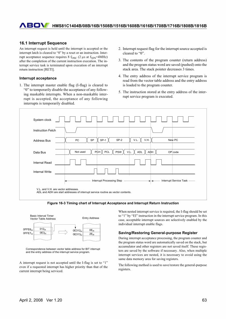
HMS81C1404B/08B/16B/1508B/1516B/1608B/1616B/1708B/1716B/1808B/1816B
16.1 Interrupt SequenceAn interrupt request is held until the interrupt is accepted or theinterrupt latch is cleared to “0” by a reset or an instruction. Inter-rupt acceptance sequence requires 8 fOSC (2 μs at fXIN=4MHz)after the completion of the current instruction execution. The in-terrupt service task is terminated upon execution of an interruptreturn instruction [RETI].
Interrupt acceptance
1. The interrupt master enable flag (I-flag) is cleared to“0” to temporarily disable the acceptance of any follow-ing maskable interrupts. When a non-maskable inter-rupt is accepted, the acceptance of any followinginterrupts is temporarily disabled.
2. Interrupt request flag for the interrupt source accepted iscleared to “0”.
3. The contents of the program counter (return address)and the program status word are saved (pushed) onto thestack area. The stack pointer decreases 3 times.
4. The entry address of the interrupt service program isread from the vector table address and the entry addressis loaded to the program counter.
5. The instruction stored at the entry address of the inter-rupt service program is executed.
Figure 16-3 Timing chart of Interrupt Acceptance and Interrupt Return Instruction
A interrupt request is not accepted until the I-flag is set to “1”even if a requested interrupt has higher priority than that of thecurrent interrupt being serviced.
When nested interrupt service is required, the I-flag should be setto “1” by “EI” instruction in the interrupt service program. In thiscase, acceptable interrupt sources are selectively enabled by theindividual interrupt enable flags.
Saving/Restoring General-purpose RegisterDuring interrupt acceptance processing, the program counter andthe program status word are automatically saved on the stack, butaccumulator and other registers are not saved itself. These regis-ters are saved by the software if necessary. Also, when multipleinterrupt services are nested, it is necessary to avoid using thesame data memory area for saving registers.
The following method is used to save/restore the general-purposeregisters.
V.L.
System clock
Address Bus PC SP SP-1 SP-2 V.H. New PC
V.L.Data Bus Not used PCH PCL PSW ADL OP codeADH
Instruction Fetch
Internal Read
Internal Write
Interrupt Processing Step Interrupt Service Task
V.L. and V.H. are vector addresses.ADL and ADH are start addresses of interrupt service routine as vector contents.
Basic Interval Timer
012H0E3H
0FFE6H0FFE7H
0EH2EH
0E312H0E313H
Entry Address
Correspondence between vector table address for BIT interruptand the entry address of the interrupt service program.
Vector Table Address
April 2, 2008 Ver 1.20 63
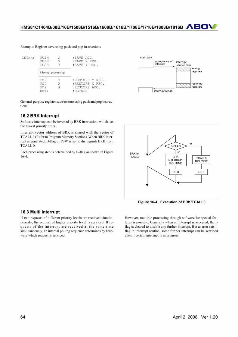
HMS81C1404B/08B/16B/1508B/1516B/1608B/1616B/1708B/1716B/1808B/1816B
Example: Register save using push and pop instructions
General-purpose register save/restore using push and pop instruc-tions;
16.2 BRK InterruptSoftware interrupt can be invoked by BRK instruction, which hasthe lowest priority order.
Interrupt vector address of BRK is shared with the vector ofTCALL 0 (Refer to Program Memory Section). When BRK inter-rupt is generated, B-flag of PSW is set to distinguish BRK fromTCALL 0.
Each processing step is determined by B-flag as shown in Figure16-4.
Figure 16-4 Execution of BRK/TCALL0
16.3 Multi InterruptIf two requests of different priority levels are received simulta-neously, the request of higher priority level is serviced. If re-quests of the interrupt are received at the same timesimultaneously, an internal polling sequence determines by hard-ware which request is serviced.
However, multiple processing through software for special fea-tures is possible. Generally when an interrupt is accepted, the I-flag is cleared to disable any further interrupt. But as user sets I-flag in interrupt routine, some further interrupt can be servicedeven if certain interrupt is in progress.
INTxx: PUSH APUSH XPUSH Y
;SAVE ACC.;SAVE X REG.;SAVE Y REG.
interrupt processing
POP YPOP XPOP ARETI
;RESTORE Y REG.;RESTORE X REG.;RESTORE ACC.;RETURN
main taskinterruptservice task
savingregisters
restoringregisters
acceptance ofinterrupt
interrupt return
B-FLAG
BRKINTERRUPT
ROUTINE
RETI
TCALL0ROUTINE
RET
BRK orTCALL0
=0
=1
64 April 2, 2008 Ver 1.20
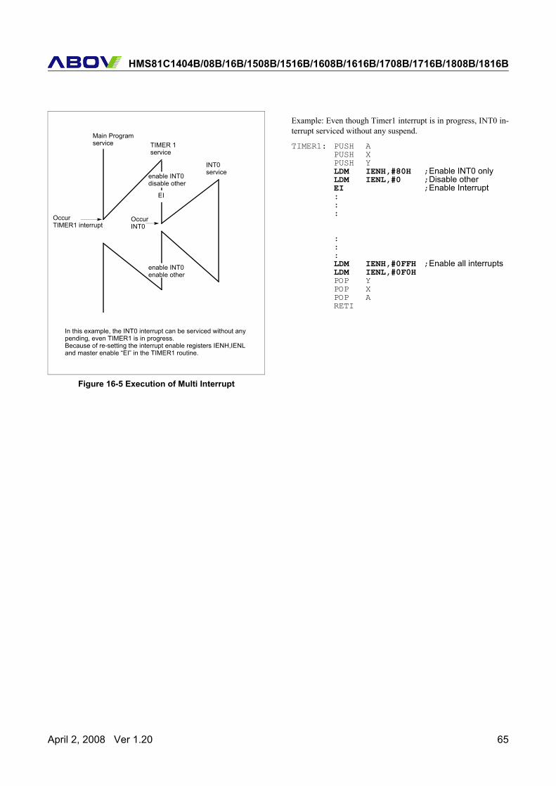
HMS81C1404B/08B/16B/1508B/1516B/1608B/1616B/1708B/1716B/1808B/1816B
Figure 16-5 Execution of Multi Interrupt
Example: Even though Timer1 interrupt is in progress, INT0 in-terrupt serviced without any suspend.
TIMER1: PUSH APUSH XPUSH YLDM IENH,#80H ;Enable INT0 onlyLDM IENL,#0 ;Disable otherEI ;Enable Interrupt:::
:::LDM IENH,#0FFH ;Enable all interruptsLDM IENL,#0F0HPOP YPOP XPOP ARETI
enable INT0
TIMER 1service
INT0service
Main Programservice
OccurTIMER1 interrupt
OccurINT0
EI
disable other
enable INT0enable other
In this example, the INT0 interrupt can be serviced without anypending, even TIMER1 is in progress.Because of re-setting the interrupt enable registers IENH,IENLand master enable “EI” in the TIMER1 routine.
April 2, 2008 Ver 1.20 65
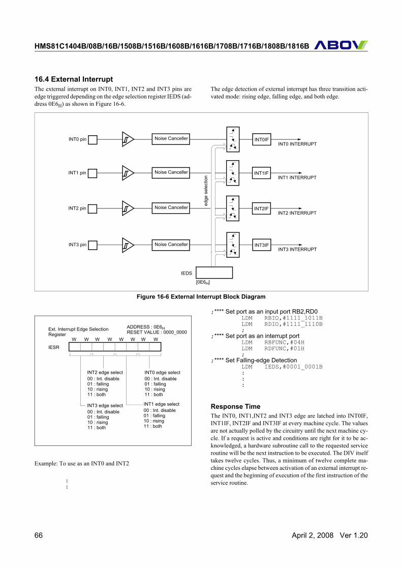
HMS81C1404B/08B/16B/1508B/1516B/1608B/1616B/1708B/1716B/1808B/1816B
16.4 External InterruptThe external interrupt on INT0, INT1, INT2 and INT3 pins areedge triggered depending on the edge selection register IEDS (ad-dress 0E6H) as shown in Figure 16-6.
The edge detection of external interrupt has three transition acti-vated mode: rising edge, falling edge, and both edge.
Figure 16-6 External Interrupt Block Diagram
Example: To use as an INT0 and INT2
::
;**** Set port as an input port RB2,RD0LDM RBIO,#1111_1011BLDM RDIO,#1111_1110B;
;**** Set port as an interrupt portLDM RBFUNC,#04HLDM RDFUNC,#01H;
;**** Set Falling-edge DetectionLDM IEDS,#0001_0001B:::
Response TimeThe INT0, INT1,INT2 and INT3 edge are latched into INT0IF,INT1IF, INT2IF and INT3IF at every machine cycle. The valuesare not actually polled by the circuitry until the next machine cy-cle. If a request is active and conditions are right for it to be ac-knowledged, a hardware subroutine call to the requested serviceroutine will be the next instruction to be executed. The DIV itselftakes twelve cycles. Thus, a minimum of twelve complete ma-chine cycles elapse between activation of an external interrupt re-quest and the beginning of execution of the first instruction of theservice routine.
INT0IFINT0 pinINT0 INTERRUPT
INT1IFINT1 pinINT1 INTERRUPT
INT2IFINT2 pinINT2 INTERRUPT
IEDS
[0E6H]
edge
sel
ectio
n
INT3IFINT3 pinINT3 INTERRUPT
Noise Canceller
Noise Canceller
Noise Canceller
Noise Canceller
INT0 edge select
Ext. Interrupt Edge Selection
IESR
ADDRESS : 0E6HRESET VALUE : 0000_0000
00 : Int. disable
W W W W W W
01 : falling10 : rising11 : both
INT1 edge selectINT3 edge select
00 : Int. disable01 : falling10 : rising11 : both
00 : Int. disable01 : falling10 : rising11 : both
RegisterW W
INT2 edge select00 : Int. disable01 : falling10 : rising11 : both
66 April 2, 2008 Ver 1.20
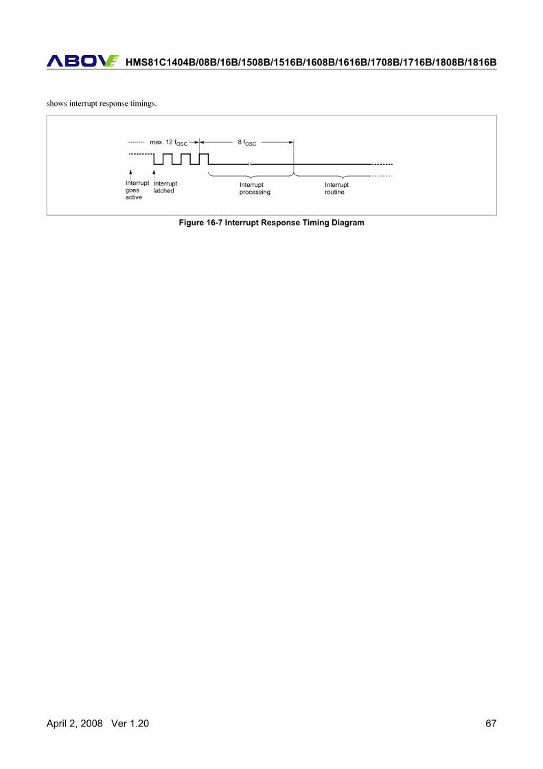
HMS81C1404B/08B/16B/1508B/1516B/1608B/1616B/1708B/1716B/1808B/1816B
shows interrupt response timings.
Figure 16-7 Interrupt Response Timing Diagram
Interruptgoesactive
Interruptlatched
Interruptprocessing
Interruptroutine
8 fOSCmax. 12 fOSC
April 2, 2008 Ver 1.20 67
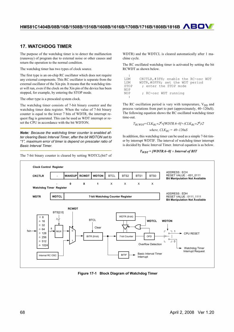
HMS81C1404B/08B/16B/1508B/1516B/1608B/1616B/1708B/1716B/1808B/1816B
17. WATCHDOG TIMERThe purpose of the watchdog timer is to detect the malfunction(runaway) of program due to external noise or other causes andreturn the operation to the normal condition.
The watchdog timer has two types of clock source.
The first type is an on-chip RC oscillator which does not requireany external components. This RC oscillator is separate from theexternal oscillator of the Xin pin. It means that the watchdog tim-er will run, even if the clock on the Xin pin of the device has beenstopped, for example, by entering the STOP mode.
The other type is a prescaled system clock.
The watchdog timer consists of 7-bit binary counter and thewatchdog timer data register. When the value of 7-bit binarycounter is equal to the lower 7 bits of WDTR, the interrupt re-quest flag is generated. This can be used as WDT interrupt or re-set the CPU in accordance with the bit WDTON.
Note: Because the watchdog timer counter is enabled af-ter clearing Basic Interval Timer, after the bit WDTON set to“1”, maximum error of timer is depend on prescaler ratio ofBasic Interval Timer.
The 7-bit binary counter is cleared by setting WDTCL(bit7 of
WDTR) and the WDTCL is cleared automatically after 1 ma-chine cycle.
The RC oscillated watchdog timer is activated by setting the bitRCWDT as shown below.
The RC oscillation period is vary with temperature, VDD andprocess variations from part to part (approximately, 40~120uS).The following equation shows the RC oscillated watchdog timertime-out.
TRCWDT=CLKRC×28×[WDTR.6~0]+(CLKRC×28)/2
where, CLKRC = 40~120uS
In addition, this watchdog timer can be used as a simple 7-bit tim-er by interrupt WDTIF. The interval of watchdog timer interruptis decided by Basic Interval Timer. Interval equation is as below.
TWDT = [WDTR.6~0] × Interval of BIT
Figure 17-1 Block Diagram of Watchdog Timer
: LDM CKCTLR,#3FH; enable the RC-osc WDT LDM WDTR,#0FFH; set the WDT periodSTOP ; enter the STOP modeNOPNOP ; RC-osc WDT running :
÷ 8÷ 16
÷ 128÷ 256÷ 512÷ 1024
÷ 32÷ 64 0
1
MUX8
3
fxin
BITR (8-bit)
BTS[2:0]RCWDT
Internal RC OSCBasic Interval TimerInterrupt
BTCL
Clear
Watchdog Timer
BITIF
7-bit Counter
WDTR (8-bit)
OFD
WDTCL WDTON
Interrupt Request
CPU RESET1
0
Clock Control Register
CKCTLRADDRESS : ECHRESET VALUE : -001_0111- WAKEUP RCWDT WDTON BTCL BTS2 BTS1 BTS0
- 0 X 1 X X X XWatchdog Timer Register
WDTRADDRESS : EDHRESET VALUE : 0111_1111WDTCL 7-bit Watchdog Counter Register
Overflow Detection
Bit Manipulation Not Available
Bit Manipulation Not Available
68 April 2, 2008 Ver 1.20
HMS81C1404B/08B/16B/1508B/1516B/1608B/1616B/1708B/1716B/1808B/1816B
18. Power Saving ModeFor applications where power consumption is a critical factor,this device provides two kinds of power saving functions, STOPmode and Wake-up Timer mode.
The power saving function is activated by execution of STOP in-
struction after setting the corresponding status (WAKEUP) ofCKCTLR.
Table 18-1shows the status of each Power Saving Mode.
18.1 Stop ModeIn the Stop mode, the on-chip oscillator is stopped. With the clockfrozen, all functions are stopped, but the on-chip RAM and Con-trol registers are held. The port pins out the values held by theirrespective port data register, port direction registers. Oscillatorstops and the systems internal operations are all held up.
• The states of the RAM, registers, and latches valid immediately before the system is put in the STOP state are all held.
• The program counter stop the address of the instruction to be executed after the instruction “STOP” which starts the STOP operating mode.
The Stop mode is activated by execution of STOP instructionafter clearing the bit WAKEUP of CKCTLR to “0”. (Thisregister should be written by byte operation. If this register isset by bit manipulation instruction, for example “set1” or“clr1” instruction, it may be undesired operation)
In the Stop mode of operation, VDD can be reduced to minimizepower consumption. Care must be taken, however, to ensure thatVDD is not reduced before the Stop mode is invoked, and thatVDD is restored to its normal operating level, before the Stopmode is terminated.
The reset should not be activated before VDD is restored to itsnormal operating level, and must be held active long enough toallow the oscillator to restart and stabilize.
Note: After STOP instruction, at least two or more NOP in-struction should be writtenEx) LDM CKCTLR,#0000_1110B
STOPNOPNOP
In the STOP operation, the dissipation of the power associatedwith the oscillator and the internal hardware is lowered; however,the power dissipation associated with the pin interface (depend-ing on the external circuitry and program) is not directly deter-mined by the hardware operation of the STOP feature. This pointshould be little current flows when the input level is stable at thepower voltage level (VDD/VSS); however, when the input levelgets higher than the power voltage level (by approximately 0.3 to0.5V), a current begins to flow. Therefore, if cutting off the out-put transistor at an I/O port puts the pin signal into the high-im-pedance state, a current flow across the ports input transistor,requiring to fix the level by pull-up or other means.
Note: The STOP mode can not be operated in internal4MHz oscillation. Other clock source like cystal, ceramicresonator or external RC oscillation should be used in theapplication using STOP mode.
Peripheral STOP Wake-up Timer
RAM Retain Retain
Control Registers Retain Retain
I/O Ports Retain Retain
CPU Stop Stop
Timer0, Timer2 Stop Operation
Oscillation Stop Oscillation
Prescaler Stop ÷ 2048 only
Entering Condition [WAKEUP] 0 1
Release Sources RESET, RCWDT, INT0~3, EC0~1, SPI
RESET, RCWDT, INT0~3, EC0~1, SPI, TIMER0, TIMER2
Table 18-1 Power Saving Mode
April 2, 2008 Ver 1.20 69
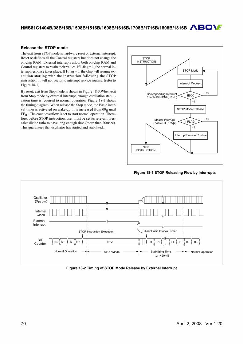
HMS81C1404B/08B/16B/1508B/1516B/1608B/1616B/1708B/1716B/1808B/1816B
Release the STOP modeThe exit from STOP mode is hardware reset or external interrupt.Reset re-defines all the Control registers but does not change theon-chip RAM. External interrupts allow both on-chip RAM andControl registers to retain their values. If I-flag = 1, the normal in-terrupt response takes place. If I-flag = 0, the chip will resume ex-ecution starting with the instruction following the STOPinstruction. It will not vector to interrupt service routine. (refer toFigure 18-1)
By reset, exit from Stop mode is shown in Figure 18-3.When exitfrom Stop mode by external interrupt, enough oscillation stabili-zation time is required to normal operation. Figure 18-2 showsthe timing diagram. When release the Stop mode, the Basic inter-val timer is activated on wake-up. It is increased from 00H untilFFH . The count overflow is set to start normal operation. There-fore, before STOP instruction, user must be set its relevant pres-caler divide ratio to have long enough time (more than 20msec).This guarantees that oscillator has started and stabilized..
Figure 18-1 STOP Releasing Flow by Interrupts
Figure 18-2 Timing of STOP Mode Release by External Interrupt
IEXX
=0
=1
STOPINSTRUCTION
STOP Mode
Interrupt Request
STOP Mode Release
I-FLAG
=1
Interrupt Service Routine
NextINSTRUCTION
=0
Master InterruptEnable Bit PSW[2]
Corresponding InterruptEnable Bit (IENH, IENL)
~~
STOP Mode Normal Operation
Oscillator(XIN pin)
~~~~
N+1N N+2 00 01 FE FF 00 00N-1N-2
~~~~
~~~~
~~
Clear Basic Interval TimerSTOP Instruction Execution
Normal Operation Stabilizing TimetST > 20mS
InternalClock
ExternalInterrupt
BITCounter
~~
70 April 2, 2008 Ver 1.20
HMS81C1404B/08B/16B/1508B/1516B/1608B/1616B/1708B/1716B/1808B/1816B
Figure 18-3 Timing of STOP Mode Release by RESET
18.2 STOP Mode using Internal RCWDT In the STOP mode using Internal RC-Oscillated Watchdog Tim-er, the on-chip oscillator is stopped. But internal RC oscillationcircuit is oscillated in this mode. The on-chip RAM and Controlregisters are held. The port pins out the values held by their re-spective port data register, port direction registers.
The Internal RC-Oscillated Watchdog Timer mode is activat-ed by setting the bit RCWDT of CKCTLR to “1”. ( This reg-ister should be written by byte operation. If this register is setby bit manipulation instruction, for example “set1” or “clr1”instruction, it may be undesired operation )
Note: After STOP instruction, at least two or more NOP in-struction should be writtenEx) LDM WDTR,#1111_1111B
LDM CKCTLR,#0010_1110BSTOPNOPNOP
Release the STOP mode using internal RCWDTThe exit from STOP mode using Internal RC-Oscillated Watch-dog Timer is hardware reset or external interrupt. Reset re-de-fines all the Control registers but does not change the on-chipRAM. External interrupts allow both on-chip RAM and Control
registers to retain their values.
If I-flag = 1, the normal interrupt response takes place. In thiscase, if the bit WDTON of CKCTLR is set to “0” and the bitWDTE of IENH is set to “1”, the device will execute the watch-dog timer interrupt service routine.(Figure 18-4) However, if thebit WDTON of CKCTLR is set to “1”, the device will generatethe internal RESET signal and execute the reset processing. (Fig-ure 18-5)
If I-flag = 0, the chip will resume execution starting with the in-struction following the STOP instruction. It will not vector to in-terrupt service routine.( refer to Figure 18-1)
When exit from STOP mode using Internal RC-OscillatedWatchdog Timer by external interrupt, the oscillation stabiliza-tion time is required to normal operation. Figure 18-4 shows thetiming diagram. When release the Internal RC-Oscillated Watch-dog Timer mode, the basic interval timer is activated on wake-up.It is increased from 00H until FFH . The count overflow is set tostart normal operation. Therefore, before STOP instruction, usermust be set its relevant prescaler divide ratio to have long enoughtime (more than 20msec). This guarantees that oscillator hasstarted and stabilized.
By reset, exit from STOP mode using internal RC-OscillatedWatchdog Timer is shown in Figure 18-5.
~~
STOP Mode
Time can not be control by software
Oscillator(XIN pin)
~~~~
~~
STOP Instruction ExecutionStabilizing Time
tST = 64mS @4MHz
InternalClock
Internal
~~~~
~~
~~ ~~RESET
RESET
April 2, 2008 Ver 1.20 71
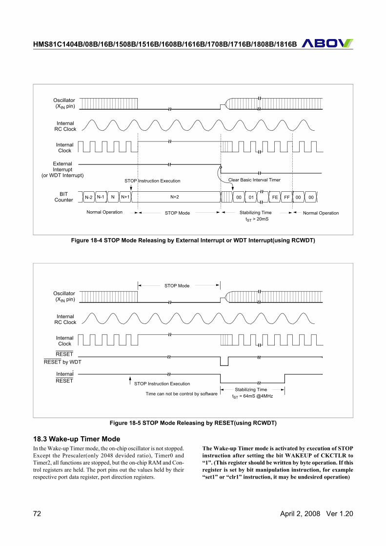
HMS81C1404B/08B/16B/1508B/1516B/1608B/1616B/1708B/1716B/1808B/1816B
Figure 18-4 STOP Mode Releasing by External Interrupt or WDT Interrupt(using RCWDT)
Figure 18-5 STOP Mode Releasing by RESET(using RCWDT)
18.3 Wake-up Timer ModeIn the Wake-up Timer mode, the on-chip oscillator is not stopped.Except the Prescaler(only 2048 devided ratio), Timer0 andTimer2, all functions are stopped, but the on-chip RAM and Con-trol registers are held. The port pins out the values held by theirrespective port data register, port direction registers.
The Wake-up Timer mode is activated by execution of STOPinstruction after setting the bit WAKEUP of CKCTLR to“1”. (This register should be written by byte operation. If thisregister is set by bit manipulation instruction, for example“set1” or “clr1” instruction, it may be undesired operation)
~~STOP Mode Normal Operation
Oscillator(XIN pin)
~~~~
N+1N N+2 00 01 FE FF 00 00N-1N-2
~~~~
~~~~
~~
Clear Basic Interval TimerSTOP Instruction Execution
Normal Operation Stabilizing TimetST > 20mS
InternalClock
ExternalInterrupt
BITCounter
~~Internal
RC Clock
(or WDT Interrupt)
~~
Oscillator(XIN pin)
~~
~~~~
~~
InternalClock
InternalRC Clock
Time can not be control by software
~~
STOP Instruction ExecutionStabilizing Time
tST = 64mS @4MHz
Internal
~~
~~ ~~
RESET by WDT
RESET
RESET
STOP Mode
72 April 2, 2008 Ver 1.20
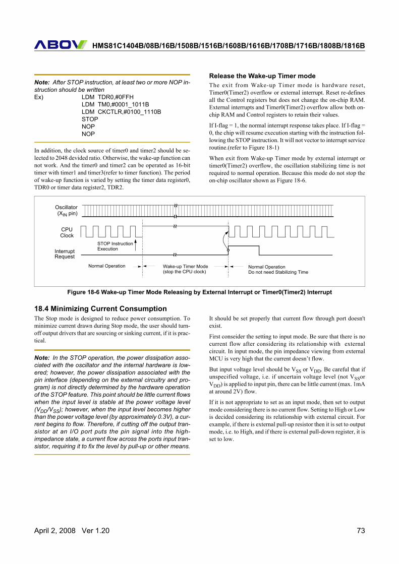
HMS81C1404B/08B/16B/1508B/1516B/1608B/1616B/1708B/1716B/1808B/1816B
Note: After STOP instruction, at least two or more NOP in-struction should be writtenEx) LDM TDR0,#0FFH
LDM TM0,#0001_1011BLDM CKCTLR,#0100_1110BSTOPNOPNOP
In addition, the clock source of timer0 and timer2 should be se-lected to 2048 devided ratio. Otherwise, the wake-up function cannot work. And the timer0 and timer2 can be operated as 16-bittimer with timer1 and timer3(refer to timer function). The periodof wake-up function is varied by setting the timer data register0,TDR0 or timer data register2, TDR2.
Release the Wake-up Timer modeThe exit from Wake-up Timer mode is hardware reset,Timer0(Timer2) overflow or external interrupt. Reset re-definesall the Control registers but does not change the on-chip RAM.External interrupts and Timer0(Timer2) overflow allow both on-chip RAM and Control registers to retain their values.
If I-flag = 1, the normal interrupt response takes place. If I-flag =0, the chip will resume execution starting with the instruction fol-lowing the STOP instruction. It will not vector to interrupt serviceroutine.(refer to Figure 18-1)
When exit from Wake-up Timer mode by external interrupt ortimer0(Timer2) overflow, the oscillation stabilizing time is notrequired to normal operation. Because this mode do not stop theon-chip oscillator shown as Figure 18-6.
Figure 18-6 Wake-up Timer Mode Releasing by External Interrupt or Timer0(Timer2) Interrupt
18.4 Minimizing Current ConsumptionThe Stop mode is designed to reduce power consumption. Tominimize current drawn during Stop mode, the user should turn-off output drivers that are sourcing or sinking current, if it is prac-tical.
Note: In the STOP operation, the power dissipation asso-ciated with the oscillator and the internal hardware is low-ered; however, the power dissipation associated with thepin interface (depending on the external circuitry and pro-gram) is not directly determined by the hardware operationof the STOP feature. This point should be little current flowswhen the input level is stable at the power voltage level(VDD/VSS); however, when the input level becomes higherthan the power voltage level (by approximately 0.3V), a cur-rent begins to flow. Therefore, if cutting off the output tran-sistor at an I/O port puts the pin signal into the high-impedance state, a current flow across the ports input tran-sistor, requiring it to fix the level by pull-up or other means.
It should be set properly that current flow through port doesn'texist.
First conseider the setting to input mode. Be sure that there is nocurrent flow after considering its relationship with externalcircuit. In input mode, the pin impedance viewing from externalMCU is very high that the current doesn’t flow.
But input voltage level should be VSS or VDD. Be careful that ifunspecified voltage, i.e. if uncertain voltage level (not VSSorVDD) is applied to input pin, there can be little current (max. 1mAat around 2V) flow.
If it is not appropriate to set as an input mode, then set to outputmode considering there is no current flow. Setting to High or Lowis decided considering its relationship with external circuit. Forexample, if there is external pull-up resistor then it is set to outputmode, i.e. to High, and if there is external pull-down register, it isset to low.
Wake-up Timer Mode
Oscillator(XIN pin)
~~
STOP Instruction
Normal Operation Normal Operation
CPUClock
RequestInterrupt
~~~~
Execution
Do not need Stabilizing Time(stop the CPU clock)
~~
April 2, 2008 Ver 1.20 73
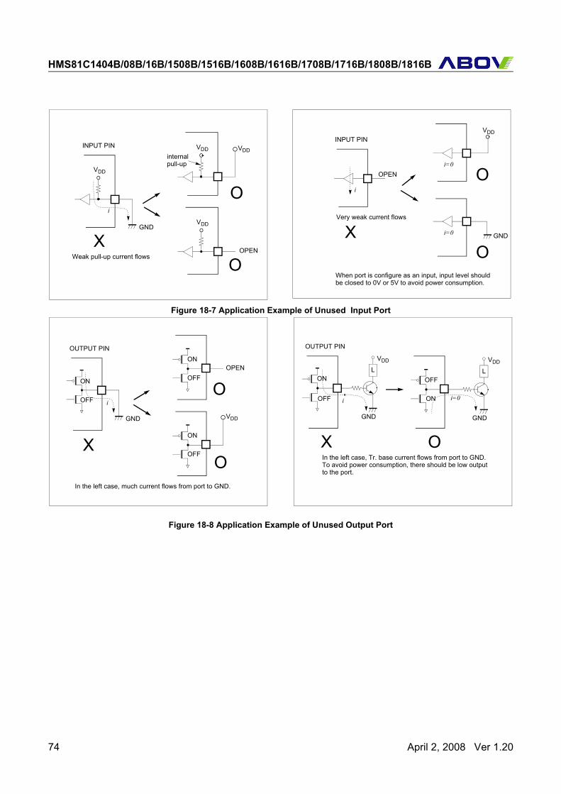
HMS81C1404B/08B/16B/1508B/1516B/1608B/1616B/1708B/1716B/1808B/1816B
Figure 18-7 Application Example of Unused Input Port
Figure 18-8 Application Example of Unused Output Port
INPUT PIN
VDD
GND
i
VDD
XWeak pull-up current flows
VDDinternalpull-up
INPUT PIN
i
VDD
XVery weak current flows
VDD
O
OOPEN
OPENi=0
O
i=0
OGND
When port is configure as an input, input level shouldbe closed to 0V or 5V to avoid power consumption.
OUTPUT PIN
GND
i
In the left case, much current flows from port to GND.
X
ON
OFF
OUTPUT PIN
GND
i
In the left case, Tr. base current flows from port to GND.
i=0
X
OFF
ON
VDD
LON
OFFOPEN
GND
VDD
L
ON
OFF
To avoid power consumption, there should be low output
ON
OFF
O
O
VDD
Oto the port.
74 April 2, 2008 Ver 1.20
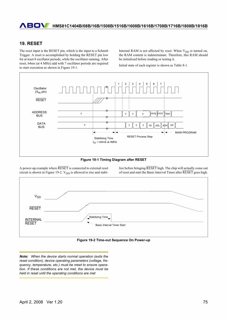
HMS81C1404B/08B/16B/1508B/1516B/1608B/1616B/1708B/1716B/1808B/1816B
19. RESETThe reset input is the RESET pin, which is the input to a SchmittTrigger. A reset is accomplished by holding the RESET pin lowfor at least 8 oscillator periods, while the oscillator running. Afterreset, 64ms (at 4 MHz) add with 7 oscillator periods are requiredto start execution as shown in Figure 19-1.
Internal RAM is not affected by reset. When VDD is turned on,the RAM content is indeterminate. Therefore, this RAM shouldbe initialized before reading or testing it.
Initial state of each register is shown as Table 8-1.
Figure 19-1 Timing Diagram after RESET
A power-up example where RESET is connected to external resetcircuit is shown in Figure 19-2. VDD is allowed to rise and stabi-
lize before bringing RESET high. The chip will actually come outof reset and start the Basic Interval Timer after RESET goes high.
Figure 19-2 Time-out Sequence On Power-up
Note: When the device starts normal operation (exits thereset condition), device operating parameters (voltage, fre-quency, temperature, etc.) must be meet to ensure opera-tion. If these conditions are not met, the device must beheld in reset until the operating conditions are met
MAIN PROGRAM
Oscillator(XIN pin)
? ? FFFE FFFF
Stabilizing TimetST = 64mS at 4MHz
RESET
ADDRESS
DATA
1 2 3 4 5 6 7
? ? Start
? ?? FE? ADL ADH OP
BUS
BUS
RESET Process Step
~~~~
~~~~
~~~~
VDD
RESET
INTERNALBasic Interval Timer Start RESET
Stabilizing Time
April 2, 2008 Ver 1.20 75
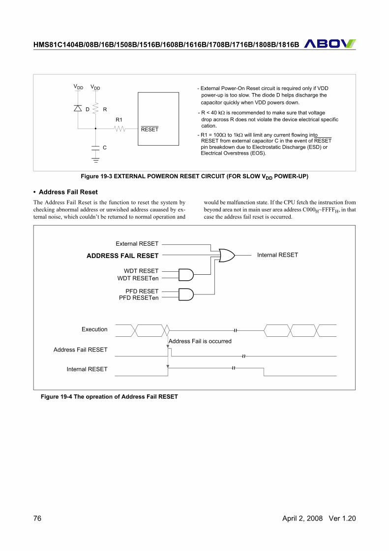
HMS81C1404B/08B/16B/1508B/1516B/1608B/1616B/1708B/1716B/1808B/1816B
Figure 19-3 EXTERNAL POWERON RESET CIRCUIT (FOR SLOW VDD POWER-UP)
• Address Fail ResetThe Address Fail Reset is the function to reset the system bychecking abnormal address or unwished address cauased by ex-ternal noise, which couldn’t be returned to normal operation and
would be malfunction state. If the CPU fetch the instruction frombeyond area not in main user area address C000H~FFFFH, in thatcase the address fail reset is occurred.
Figure 19-4 The opreation of Address Fail RESET
RESET
- External Power-On Reset circuit is required only if VDD power-up is too slow. The diode D helps discharge the capacitor quickly when VDD powers down.
- R < 40 kΩ is recommended to make sure that voltage drop across R does not violate the device electrical specificcation.
- R1 = 100Ω to 1kΩ will limit any current flowing into RESET from external capacitor C in the event of RESET pin breakdown due to Electrostatic Discharge (ESD) or Electrical Overstress (EOS).
R
R1
D
C
VDDVDD
External RESET
ADDRESS FAIL RESET
WDT RESETWDT RESETen
PFD RESETPFD RESETen
Execution
Address Fail RESET
Internal RESET
Address Fail is occurred
~~~~
~~
Internal RESET
76 April 2, 2008 Ver 1.20
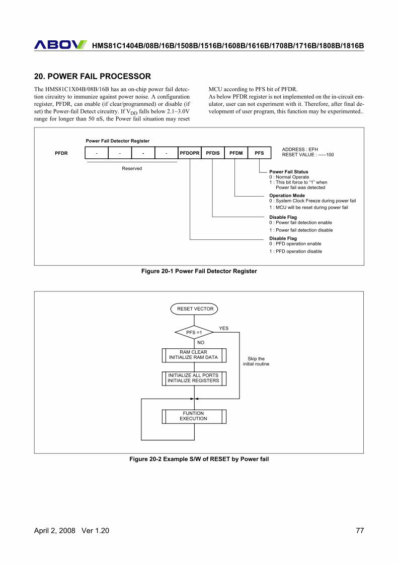
HMS81C1404B/08B/16B/1508B/1516B/1608B/1616B/1708B/1716B/1808B/1816B
20. POWER FAIL PROCESSORThe HMS81C1X04B/08B/16B has an on-chip power fail detec-tion circuitry to immunize against power noise. A configurationregister, PFDR, can enable (if clear/programmed) or disable (ifset) the Power-fail Detect circuitry. If VDD falls below 2.1~3.0Vrange for longer than 50 nS, the Power fail situation may reset
MCU according to PFS bit of PFDR.As below PFDR register is not implemented on the in-circuit em-ulator, user can not experiment with it. Therefore, after final de-velopment of user program, this function may be experimented..
Figure 20-1 Power Fail Detector Register
Figure 20-2 Example S/W of RESET by Power fail
PFDRADDRESS : EFHRESET VALUE : -----100- - - - PFDOPR PFDIS PFDM PFS
ReservedPower Fail Status0 : Normal Operate1 : This bit force to “1” when
Operation Mode0 : System Clock Freeze during power fail1 : MCU will be reset during power fail
Disable Flag0 : Power fail detection enable1 : Power fail detection disable
Power Fail Detector Register
Power fail was detected
Disable Flag0 : PFD operation enable1 : PFD operation disable
FUNTIONEXECUTION
INITIALIZE RAM DATA
PFS =1
NO
RESET VECTOR
INITIALIZE ALL PORTSINITIALIZE REGISTERS
RAM CLEAR
YES
Skip theinitial routine
April 2, 2008 Ver 1.20 77
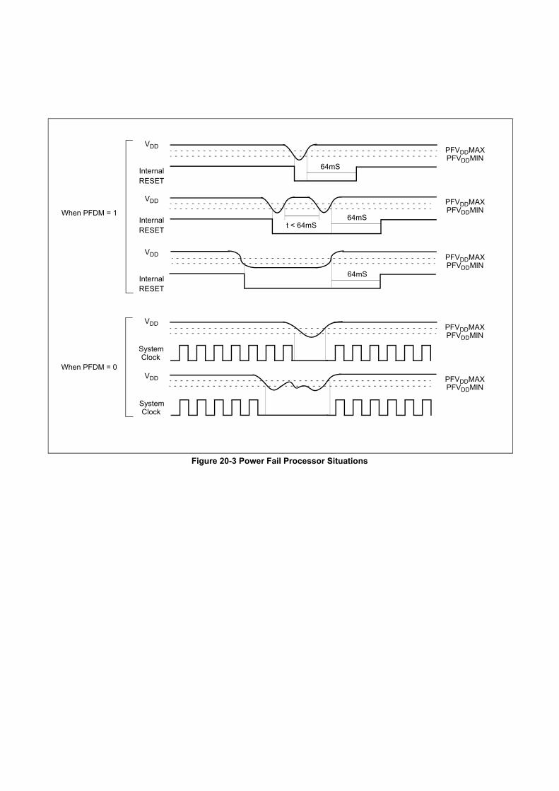
Figure 20-3 Power Fail Processor Situations
InternalRESET
InternalRESET
InternalRESET
VDD
VDD
VDD
PFVDDMAXPFVDDMIN
PFVDDMAXPFVDDMIN
PFVDDMAXPFVDDMIN
64mS
64mSt < 64mS
64mS
When PFDM = 1
VDD
VDD PFVDDMAXPFVDDMIN
PFVDDMAXPFVDDMIN
When PFDM = 0
SystemClock
SystemClock
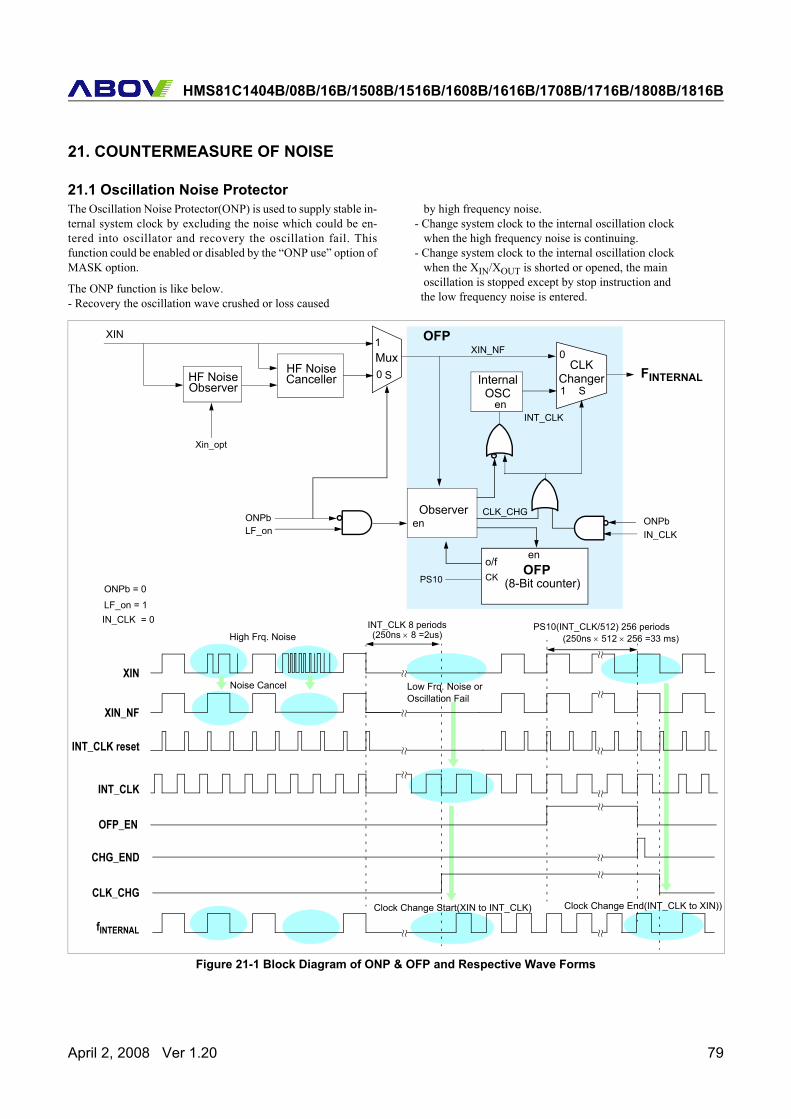
HMS81C1404B/08B/16B/1508B/1516B/1608B/1616B/1708B/1716B/1808B/1816B
21. COUNTERMEASURE OF NOISE
21.1 Oscillation Noise ProtectorThe Oscillation Noise Protector(ONP) is used to supply stable in-ternal system clock by excluding the noise which could be en-tered into oscillator and recovery the oscillation fail. Thisfunction could be enabled or disabled by the “ONP use” option ofMASK option.
The ONP function is like below.- Recovery the oscillation wave crushed or loss caused
by high frequency noise.- Change system clock to the internal oscillation clock when the high frequency noise is continuing.- Change system clock to the internal oscillation clock when the XIN/XOUT is shorted or opened, the main oscillation is stopped except by stop instruction and the low frequency noise is entered.
Figure 21-1 Block Diagram of ONP & OFP and Respective Wave Forms
LF NoiseObserver
HF NoiseCancellerHF Noise
Observer
Mux CLKChangerInternal
OSC
OFP
OFP
o/fCK
Xin_opt
PS10
FINTERNAL
INT_CLK
XIN_NFXIN
ONPbIN_CLK
(8-Bit counter)
en
ONPbLF_on
en
en
0
0
1
1
SS
ONPb = 0
LF_on = 1IN_CLK = 0
CLK_CHG
XIN_NF
INT_CLK reset
INT_CLK
OFP_EN
CHG_END
CLK_CHG
fINTERNAL
~ ~
~ ~
~ ~ ~ ~~ ~
~ ~
~ ~~ ~
~ ~~ ~
~ ~
High Frq. Noise
XIN ~ ~
~ ~
Noise Cancel
INT_CLK 8 periods(250ns × 8 =2us)
Low Frq. Noise orOscillation Fail
Clock Change Start(XIN to INT_CLK)
PS10(INT_CLK/512) 256 periods(250ns × 512 × 256 =33 ms)
Clock Change End(INT_CLK to XIN))
April 2, 2008 Ver 1.20 79
HMS81C1404B/08B/16B/1508B/1516B/1608B/1616B/1708B/1716B/1808B/1816B
21.2 Oscillation Fail ProcessorThe oscillation fail processor (OFP) can change the clock sourcefrom external to internal oscillator when the osicllation fail oc-cured. This function could be enabled or disabled by the “OFPuse” option of MASK option.And this function can recover the external clock source when theexternal clock is recovered to normal state.
HFNC OptionThe “HFNC” option is the function to control the amount of noiseto be cancelled which entered into noise canceller in ONP, ac-cording to external oscillator frequency. If the amount of noise tobe cancelled is selected to 40nS by “HFNC” option, the noisecanceller in ONP cancels the clock over 12.5MHz as a noise. Andif the amount of noise to be cancelled is selected to 80nS by
“HFNC” option, the noise canceller in ONP cancels the clockover 6.25MHz as a noise.
IN_CLK use OptionThe “IN_CLK use” Option is the function to operate the deviceby using the internal oscillator clock in ONP block as systemclock. There is no need to connect the x-tal, resonator, RC and Rexternaly. The user only to connect the XIN pin to VSS. This func-tion could be selected by the MASK option of MASK order sheet.The characteristics of internal oscillator clock has the period of250ns±10% at VDD=5V and 250ns±20% at whole operating volt-age. After selecting the IN_CLK Option, the period of internaloscillator clock could be checked by XOUT outputting clock di-vided the internal oscillator clock by 4.
21.3 Examples of ONPThe ONP operations are specified with MASK options as shownin Table 21-1. If the “ONP Use” option is set to “No”, all of theONP operations including Noice canceller, Oscillation Fail Pro-
cessor and internal 4MHz oscillation are disabled. When the in-ternal 4MHz clock is used to system clock source, the “ONP Use”option should be set to “Yes”.
Table 21-1 Examples of ONP
ONP Use IN_CLK OFP Use HFNC Description
Yes No No 40ns 40ns noise canceller
Yes No No 80ns 80ns noise canceller
Yes No Yes 40ns 40ns noise canceller + change the clock source from external to internal 4MHz clock when oscillation failure occured.
Yes No Yes 80ns 80ns noise canceller + change the clock source from external to internal 4MHz clock when oscillation failure occured
Yes Yes X X using internal 4MHz oscillator regardless of external oscillator
No X X X ONP including OFP, Noice canceller and Internal 4MHz clock disable
80 April 2, 2008 Ver 1.20
HMS81C1404B/08B/16B/1508B/1516B/1608B/1616B/1708B/1716B/1808B/1816B
22. MASK OptionThe HMS81C1X04B/08B/16B has several MASK option whichconfigures the package type or use of some special features of thedevice. The Mask option of the MASK order sheet should be
checked to select device configuration such as package type, Os-cillation selection, oscillation noise protector, oscillation fail pro-tector, internal 4MHz, amount of noise to be cancelled.
Table 22-1 MASK options
Option Check Operation Remark
MASKOption
Package28SKDIP 28SKDIP type package select This option is valid only for the
HMS1404B/08B/16B28SOP 28SOP type package select
OSC Opt.Crystal X-tal or Ceramic Oscillation for device clock source
-RC External RC/ R Oscillation for device clock source
ONP UseYes OSC Noise Protector Enable OSC Noise Protector(ONP)
Operation En/Disable BitNo OSC Noise Protector Disable
OFP UseYes Enables Oscillation Fail Processor (ONP clock
changer ) Cnange the Inter clock when oscillation failed
No Disables Oscillation Fail Processor (ONP clock changer )
HFNC40ns 40nS noise cancel (Xin : 8MHz) To select the amount of noise of
to be cancelled in ONP OSC.80ns 80nS noise cancel (Xin : 4MHz)
IN_CLKYes Enables the Internal 4MHz clock Using the internal 4MHz clock
without external oscillation circuit.No Disables the Internal 4MHz clock
April 2, 2008 Ver 1.20 81

HMS81C1404B/08B/16B/1508B/1516B/1608B/1616B/1708B/1716B/1808B/1816B
82 April 2, 2008 Ver 1.20

HMS81C1404B/08B/16B/1508B/1516B/1608B/1616B/1708B/1716B/1808B/1816B
April 2, 2008 Ver 1.20 i
APPENDIX
HMS81C1404B/08B/16B/1508B/1516B/1608B/1616B/1708B/1716B/1808B/1816B
A. INSTRUCTION
A.1 Terminology List
Terminology DescriptionA AccumulatorX X - registerY Y - register
PSW Program Status Word#imm 8-bit Immediate data
dp Direct Page Offset Address!abs Absolute Address[ ] Indirect expression{ } Register Indirect expression
{ }+ Register Indirect expression, after that, Register auto-increment.bit Bit Position
A.bit Bit Position of Accumulatordp.bit Bit Position of Direct Page MemoryM.bit Bit Position of Memory Data (000H~0FFFH)rel Relative Addressing Data
upage U-page (0FF00H~0FFFFH) Offset Addressn Table CALL Number (0~15)+ Addition
xUpper Nibble Expression in Opcode
yUpper Nibble Expression in Opcode
− Subtraction× Multiplication/ Division
( ) Contents Expression∧ AND∨ OR⊕ Exclusive OR~ NOT← Assignment / Transfer / Shift Left→ Shift Right↔ Exchange= Equal≠ Not Equal
0
Bit Position
1
Bit Position
ii April 2, 2008 Ver 1.20
HMS81C1404B/08B/16B/1508B/1516B/1608B/1616B/1708B/1716B/1808B/1816B
A.2 Instruction Map
LOWHIGH
0000000
0000101
0001002
0001103
0010004
0010105
0011006
0011107
0100008
0100109
010100A
010110B
011000C
011010D
011100E
011110F
000 - SET1dp.bit
BBSA.bit,rel
BBSdp.bit,rel
ADC#imm
ADCdp
ADCdp+X
ADC!abs
ASLA
ASLdp
TCALL0
SETA1.bit
BITdp
POPA
PUSHA BRK
001 CLRC “ “ “ SBC#imm
SBCdp
SBCdp+X
SBC!abs
ROLA
ROLdp
TCALL2
CLRA1.bit
COMdp
POPX
PUSHX
BRArel
010 CLRG “ “ “ CMP#imm
CMPdp
CMPdp+X
CMP!abs
LSRA
LSRdp
TCALL4
NOT1M.bit
TSTdp
POPY
PUSHY
PCALLUpage
011 DI “ “ “ OR#imm
ORdp
ORdp+X
OR!abs
RORA
RORdp
TCALL6
OR1OR1B
CMPXdp
POPPSW
PUSHPSW RET
100 CLRV “ “ “ AND#imm
ANDdp
ANDdp+X
AND!abs
INCA
INCdp
TCALL8
AND1AND1B
CMPYdp
CBNEdp+X TXSP INC
X
101 SETC “ “ “ EOR#imm
EORdp
EORdp+X
EOR!abs
DECA
DECdp
TCALL10
EOR1EOR1B
DBNEdp
XMAdp+X TSPX DEC
X
110 SETG “ “ “ LDA#imm
LDAdp
LDAdp+X
LDA!abs TXA LDY
dpTCALL
12LDC
LDCBLDXdp
LDXdp+Y XCN DAS
(N/A)
111 EI “ “ “ LDMdp,#imm
STAdp
STAdp+X
STA!abs TAX STY
dpTCALL
14STCM.bit
STXdp
STXdp+Y XAX STOP
LOWHIGH
1000010
1000111
1001012
1001113
1010014
1010115
1011016
1011117
1100018
1100119
110101A
110111B
111001C
111011D
111101E
111111F
000 BPLrel
CLR1dp.bit
BBCA.bit,rel
BBCdp.bit,rel
ADC{X}
ADC!abs+Y
ADC[dp+X]
ADC[dp]+Y
ASL!abs
ASLdp+X
TCALL1
JMP!abs
BIT!abs
ADDWdp
LDX#imm
JMP[!abs]
001 BVCrel “ “ “ SBC
{X}SBC
!abs+YSBC
[dp+X]SBC
[dp]+YROL!abs
ROLdp+X
TCALL3
CALL!abs
TEST!abs
SUBWdp
LDY#imm
JMP[dp]
010 BCCrel “ “ “ CMP
{X}CMP
!abs+YCMP
[dp+X]CMP
[dp]+YLSR!abs
LSRdp+X
TCALL5 MUL TCLR1
!absCMPW
dpCMPX#imm
CALL[dp]
011 BNErel “ “ “ OR
{X}OR
!abs+YOR
[dp+X]OR
[dp]+YROR!abs
RORdp+X
TCALL7
DBNEY
CMPX!abs
LDYAdp
CMPY#imm RETI
100 BMIrel “ “ “ AND
{X}AND
!abs+YAND
[dp+X]AND
[dp]+YINC!abs
INCdp+X
TCALL9 DIV CMPY
!absINCW
dpINCY TAY
101 BVSrel “ “ “ EOR
{X}EOR
!abs+YEOR
[dp+X]EOR
[dp]+YDEC!abs
DECdp+X
TCALL11
XMA{X}
XMAdp
DECWdp
DECY TYA
110 BCSrel “ “ “ LDA
{X}LDA
!abs+YLDA
[dp+X]LDA
[dp]+YLDY!abs
LDYdp+X
TCALL13
LDA{X}+
LDX!abs
STYAdp XAY DAA
(N/A)
111 BEQrel “ “ “ STA
{X}STA
!abs+YSTA
[dp+X]STA
[dp]+YSTY!abs
STYdp+X
TCALL15
STA{X}+
STX!abs
CBNEdp XYX NOP
April 2, 2008 Ver 1.20 iii
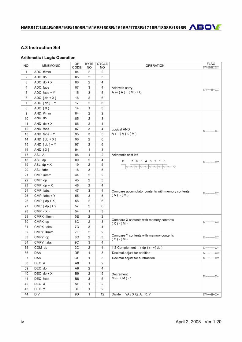
HMS81C1404B/08B/16B/1508B/1516B/1608B/1616B/1708B/1716B/1808B/1816B
A.3 Instruction Set
Arithmetic / Logic Operation
NO. MNEMONIC OPCODE
BYTENO
CYCLENO OPERATION FLAG
NVGBHIZC
1 ADC #imm 04 2 2
Add with carry.A ← ( A ) + ( M ) + C
NV--H-ZC
2 ADC dp 05 2 33 ADC dp + X 06 2 44 ADC !abs 07 3 45 ADC !abs + Y 15 3 56 ADC [ dp + X ] 16 2 67 ADC [ dp ] + Y 17 2 68 ADC { X } 14 1 39 AND #imm 84 2 2
Logical ANDA ← ( A ) ∧ ( M )
N-----Z-
10 AND dp 85 2 311 AND dp + X 86 2 412 AND !abs 87 3 413 AND !abs + Y 95 3 514 AND [ dp + X ] 96 2 615 AND [ dp ] + Y 97 2 616 AND { X } 94 1 317 ASL A 08 1 2 Arithmetic shift left
N-----ZC18 ASL dp 09 2 419 ASL dp + X 19 2 520 ASL !abs 18 3 521 CMP #imm 44 2 2
Compare accumulator contents with memory contents( A ) - ( M ) N-----ZC
22 CMP dp 45 2 323 CMP dp + X 46 2 424 CMP !abs 47 3 425 CMP !abs + Y 55 3 526 CMP [ dp + X ] 56 2 627 CMP [ dp ] + Y 57 2 628 CMP { X } 54 1 329 CMPX #imm 5E 2 2
Compare X contents with memory contents( X ) - ( M ) N-----ZC30 CMPX dp 6C 2 3
31 CMPX !abs 7C 3 432 CMPY #imm 7E 2 2
Compare Y contents with memory contents( Y ) - ( M ) N-----ZC33 CMPY dp 8C 2 3
34 CMPY !abs 9C 3 435 COM dp 2C 2 4 1’S Complement : ( dp ) ← ~( dp ) N-----Z-
36 DAA DF 1 3 Decimal adjust for addition N-----ZC
37 DAS CF 1 3 Decimal adjust for subtraction N-----ZC
38 DEC A A8 1 2
DecrementM ← ( M ) - 1 N-----Z-
39 DEC dp A9 2 440 DEC dp + X B9 2 541 DEC !abs B8 3 542 DEC X AF 1 243 DEC Y BE 1 244 DIV 9B 1 12 Divide : YA / X Q: A, R: Y NV--H-Z-
0
“0”
C 7 6 5 4 3 2 1
iv April 2, 2008 Ver 1.20
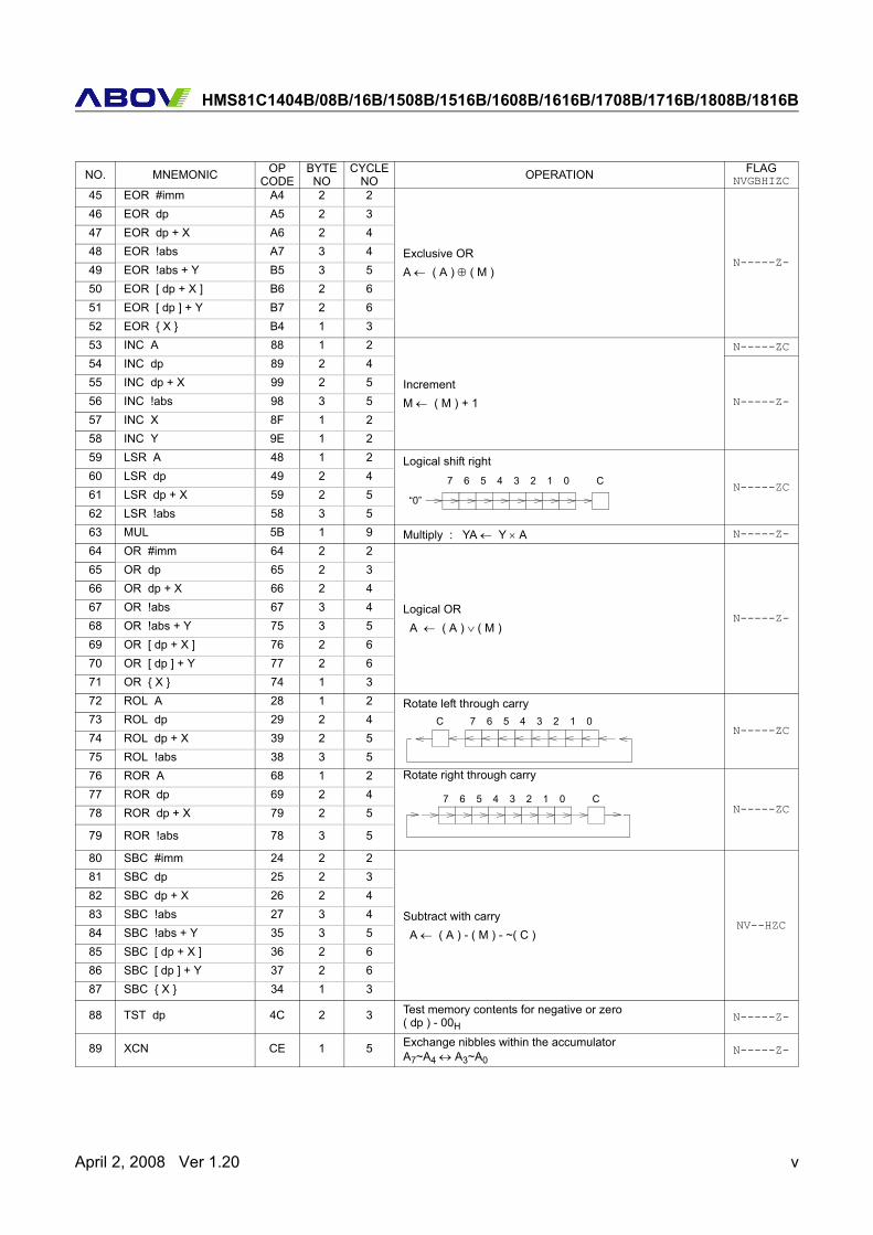
HMS81C1404B/08B/16B/1508B/1516B/1608B/1616B/1708B/1716B/1808B/1816B
45 EOR #imm A4 2 2
Exclusive ORA ← ( A ) ⊕ ( M )
N-----Z-
46 EOR dp A5 2 347 EOR dp + X A6 2 448 EOR !abs A7 3 449 EOR !abs + Y B5 3 550 EOR [ dp + X ] B6 2 651 EOR [ dp ] + Y B7 2 652 EOR { X } B4 1 353 INC A 88 1 2
IncrementM ← ( M ) + 1
N-----ZC
54 INC dp 89 2 4
N-----Z-
55 INC dp + X 99 2 556 INC !abs 98 3 557 INC X 8F 1 258 INC Y 9E 1 259 LSR A 48 1 2 Logical shift right
N-----ZC60 LSR dp 49 2 461 LSR dp + X 59 2 562 LSR !abs 58 3 563 MUL 5B 1 9 Multiply : YA ← Y × A N-----Z-
64 OR #imm 64 2 2
Logical OR A ← ( A ) ∨ ( M )
N-----Z-
65 OR dp 65 2 366 OR dp + X 66 2 467 OR !abs 67 3 468 OR !abs + Y 75 3 569 OR [ dp + X ] 76 2 670 OR [ dp ] + Y 77 2 671 OR { X } 74 1 372 ROL A 28 1 2 Rotate left through carry
N-----ZC73 ROL dp 29 2 474 ROL dp + X 39 2 575 ROL !abs 38 3 576 ROR A 68 1 2 Rotate right through carry
N-----ZC77 ROR dp 69 2 478 ROR dp + X 79 2 5
79 ROR !abs 78 3 5
80 SBC #imm 24 2 2
Subtract with carry A ← ( A ) - ( M ) - ~( C )
NV--HZC
81 SBC dp 25 2 382 SBC dp + X 26 2 483 SBC !abs 27 3 484 SBC !abs + Y 35 3 585 SBC [ dp + X ] 36 2 686 SBC [ dp ] + Y 37 2 687 SBC { X } 34 1 3
88 TST dp 4C 2 3 Test memory contents for negative or zero( dp ) - 00H
N-----Z-
89 XCN CE 1 5 Exchange nibbles within the accumulatorA7~A4 ↔ A3~A0
N-----Z-
NO. MNEMONIC OPCODE
BYTENO
CYCLENO OPERATION FLAG
NVGBHIZC
0
“0”
C7 6 5 4 3 2 1
0C 7 6 5 4 3 2 1
0 C7 6 5 4 3 2 1
April 2, 2008 Ver 1.20 v
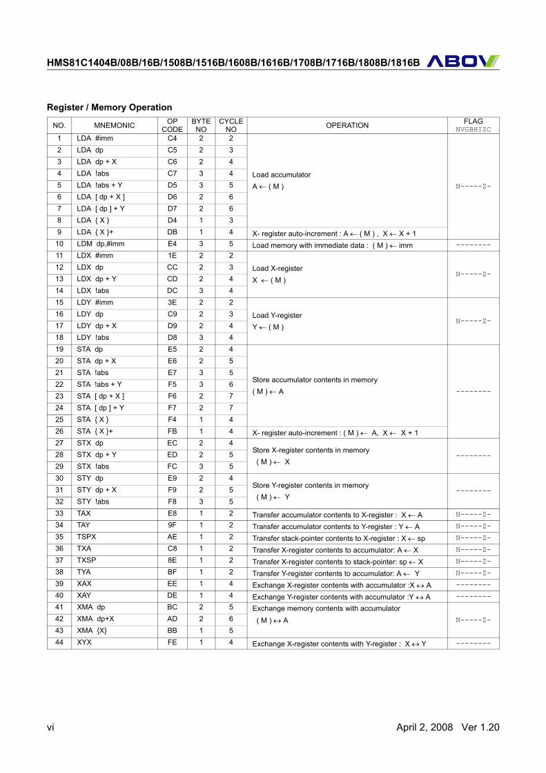
HMS81C1404B/08B/16B/1508B/1516B/1608B/1616B/1708B/1716B/1808B/1816B
Register / Memory Operation
NO. MNEMONIC OPCODE
BYTENO
CYCLENO OPERATION FLAG
NVGBHIZC1 LDA #imm C4 2 2
Load accumulatorA ← ( M ) N-----Z-
2 LDA dp C5 2 33 LDA dp + X C6 2 44 LDA !abs C7 3 45 LDA !abs + Y D5 3 56 LDA [ dp + X ] D6 2 67 LDA [ dp ] + Y D7 2 68 LDA { X } D4 1 39 LDA { X }+ DB 1 4 X- register auto-increment : A ← ( M ) , X ← X + 1
10 LDM dp,#imm E4 3 5 Load memory with immediate data : ( M ) ← imm --------
11 LDX #imm 1E 2 2
Load X-registerX ← ( M )
N-----Z-12 LDX dp CC 2 313 LDX dp + Y CD 2 414 LDX !abs DC 3 415 LDY #imm 3E 2 2
Load Y-registerY ← ( M )
N-----Z-16 LDY dp C9 2 317 LDY dp + X D9 2 418 LDY !abs D8 3 419 STA dp E5 2 4
Store accumulator contents in memory( M ) ← A --------
20 STA dp + X E6 2 521 STA !abs E7 3 522 STA !abs + Y F5 3 623 STA [ dp + X ] F6 2 724 STA [ dp ] + Y F7 2 725 STA { X } F4 1 426 STA { X }+ FB 1 4 X- register auto-increment : ( M ) ← A, X ← X + 127 STX dp EC 2 4
Store X-register contents in memory ( M ) ← X
--------28 STX dp + Y ED 2 529 STX !abs FC 3 530 STY dp E9 2 4
Store Y-register contents in memory ( M ) ← Y
--------31 STY dp + X F9 2 532 STY !abs F8 3 533 TAX E8 1 2 Transfer accumulator contents to X-register : X ← A N-----Z-
34 TAY 9F 1 2 Transfer accumulator contents to Y-register : Y ← A N-----Z-
35 TSPX AE 1 2 Transfer stack-pointer contents to X-register : X ← sp N-----Z-
36 TXA C8 1 2 Transfer X-register contents to accumulator: A ← X N-----Z-
37 TXSP 8E 1 2 Transfer X-register contents to stack-pointer: sp ← X N-----Z-
38 TYA BF 1 2 Transfer Y-register contents to accumulator: A ← Y N-----Z-
39 XAX EE 1 4 Exchange X-register contents with accumulator :X ↔ A --------
40 XAY DE 1 4 Exchange Y-register contents with accumulator :Y ↔ A --------
41 XMA dp BC 2 5 Exchange memory contents with accumulatorN-----Z-42 XMA dp+X AD 2 6 ( M ) ↔ A
43 XMA {X} BB 1 544 XYX FE 1 4 Exchange X-register contents with Y-register : X ↔ Y --------
vi April 2, 2008 Ver 1.20
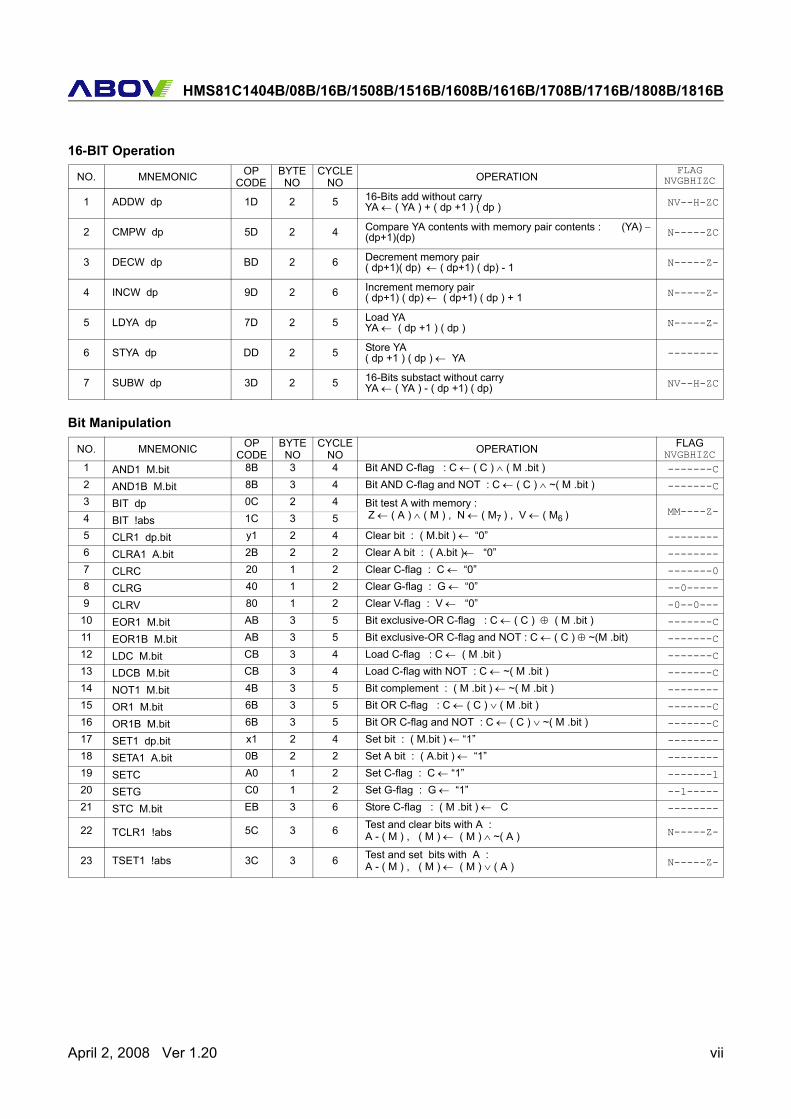
HMS81C1404B/08B/16B/1508B/1516B/1608B/1616B/1708B/1716B/1808B/1816B
16-BIT Operation
Bit Manipulation
NO. MNEMONIC OPCODE
BYTENO
CYCLENO OPERATION
FLAGNVGBHIZC
1 ADDW dp 1D 2 5 16-Bits add without carry YA ← ( YA ) + ( dp +1 ) ( dp ) NV--H-ZC
2 CMPW dp 5D 2 4 Compare YA contents with memory pair contents : (YA) − (dp+1)(dp) N-----ZC
3 DECW dp BD 2 6 Decrement memory pair( dp+1)( dp) ← ( dp+1) ( dp) - 1 N-----Z-
4 INCW dp 9D 2 6 Increment memory pair ( dp+1) ( dp) ← ( dp+1) ( dp ) + 1 N-----Z-
5 LDYA dp 7D 2 5 Load YA YA ← ( dp +1 ) ( dp ) N-----Z-
6 STYA dp DD 2 5 Store YA( dp +1 ) ( dp ) ← YA --------
7 SUBW dp 3D 2 5 16-Bits substact without carryYA ← ( YA ) - ( dp +1) ( dp) NV--H-ZC
NO. MNEMONIC OPCODE
BYTENO
CYCLENO OPERATION FLAG
NVGBHIZC1 AND1 M.bit 8B 3 4 Bit AND C-flag : C ← ( C ) ∧ ( M .bit ) -------C
2 AND1B M.bit 8B 3 4 Bit AND C-flag and NOT : C ← ( C ) ∧ ~( M .bit ) -------C
3 BIT dp 0C 2 4 Bit test A with memory : Z ← ( A ) ∧ ( M ) , N ← ( M7 ) , V ← ( M6 ) MM----Z-
4 BIT !abs 1C 3 55 CLR1 dp.bit y1 2 4 Clear bit : ( M.bit ) ← “0” --------
6 CLRA1 A.bit 2B 2 2 Clear A bit : ( A.bit )← “0” --------
7 CLRC 20 1 2 Clear C-flag : C ← “0” -------0
8 CLRG 40 1 2 Clear G-flag : G ← “0” --0-----
9 CLRV 80 1 2 Clear V-flag : V ← “0” -0--0---
10 EOR1 M.bit AB 3 5 Bit exclusive-OR C-flag : C ← ( C ) ⊕ ( M .bit ) -------C
11 EOR1B M.bit AB 3 5 Bit exclusive-OR C-flag and NOT : C ← ( C ) ⊕ ~(M .bit) -------C
12 LDC M.bit CB 3 4 Load C-flag : C ← ( M .bit ) -------C
13 LDCB M.bit CB 3 4 Load C-flag with NOT : C ← ~( M .bit ) -------C
14 NOT1 M.bit 4B 3 5 Bit complement : ( M .bit ) ← ~( M .bit ) --------
15 OR1 M.bit 6B 3 5 Bit OR C-flag : C ← ( C ) ∨ ( M .bit ) -------C
16 OR1B M.bit 6B 3 5 Bit OR C-flag and NOT : C ← ( C ) ∨ ~( M .bit ) -------C
17 SET1 dp.bit x1 2 4 Set bit : ( M.bit ) ← “1” --------
18 SETA1 A.bit 0B 2 2 Set A bit : ( A.bit ) ← “1” --------
19 SETC A0 1 2 Set C-flag : C ← “1” -------1
20 SETG C0 1 2 Set G-flag : G ← “1” --1-----
21 STC M.bit EB 3 6 Store C-flag : ( M .bit ) ← C --------
22 TCLR1 !abs 5C 3 6 Test and clear bits with A : A - ( M ) , ( M ) ← ( M ) ∧ ~( A ) N-----Z-
23 TSET1 !abs 3C 3 6 Test and set bits with A : A - ( M ) , ( M ) ← ( M ) ∨ ( A ) N-----Z-
April 2, 2008 Ver 1.20 vii
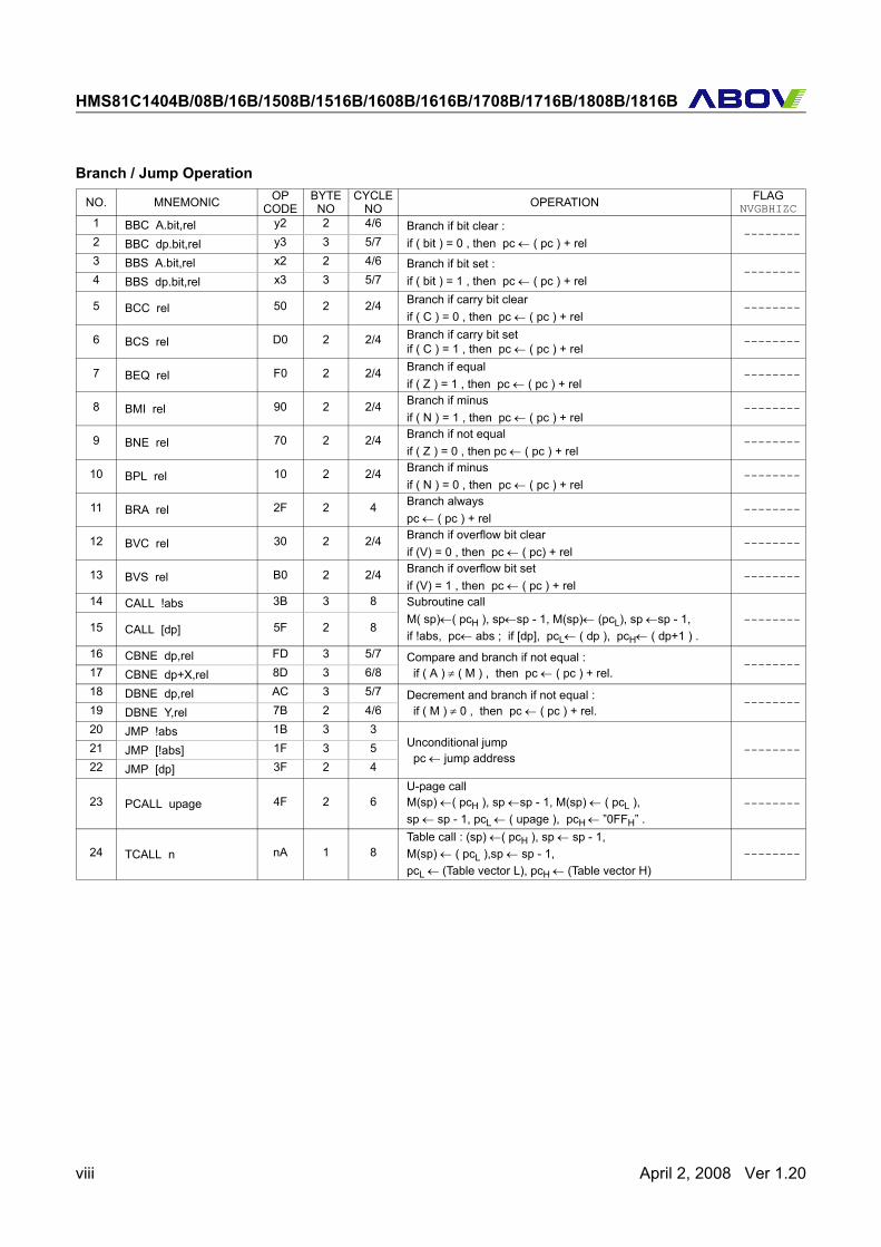
HMS81C1404B/08B/16B/1508B/1516B/1608B/1616B/1708B/1716B/1808B/1816B
Branch / Jump Operation
NO. MNEMONIC OPCODE
BYTENO
CYCLENO OPERATION FLAG
NVGBHIZC1 BBC A.bit,rel y2 2 4/6 Branch if bit clear :
if ( bit ) = 0 , then pc ← ( pc ) + rel --------
2 BBC dp.bit,rel y3 3 5/73 BBS A.bit,rel x2 2 4/6 Branch if bit set :
if ( bit ) = 1 , then pc ← ( pc ) + rel --------
4 BBS dp.bit,rel x3 3 5/7
5 BCC rel 50 2 2/4 Branch if carry bit clearif ( C ) = 0 , then pc ← ( pc ) + rel
--------
6 BCS rel D0 2 2/4 Branch if carry bit setif ( C ) = 1 , then pc ← ( pc ) + rel
--------
7 BEQ rel F0 2 2/4 Branch if equalif ( Z ) = 1 , then pc ← ( pc ) + rel
--------
8 BMI rel 90 2 2/4 Branch if minusif ( N ) = 1 , then pc ← ( pc ) + rel
--------
9 BNE rel 70 2 2/4 Branch if not equalif ( Z ) = 0 , then pc ← ( pc ) + rel
--------
10 BPL rel 10 2 2/4 Branch if minusif ( N ) = 0 , then pc ← ( pc ) + rel
--------
11 BRA rel 2F 2 4 Branch alwayspc ← ( pc ) + rel
--------
12 BVC rel 30 2 2/4 Branch if overflow bit clearif (V) = 0 , then pc ← ( pc) + rel
--------
13 BVS rel B0 2 2/4 Branch if overflow bit setif (V) = 1 , then pc ← ( pc ) + rel
--------
14 CALL !abs 3B 3 8 Subroutine callM( sp)←( pcH ), sp←sp - 1, M(sp)← (pcL), sp ←sp - 1,if !abs, pc← abs ; if [dp], pcL← ( dp ), pcH← ( dp+1 ) .
--------15 CALL [dp] 5F 2 8
16 CBNE dp,rel FD 3 5/7 Compare and branch if not equal : if ( A ) ≠ ( M ) , then pc ← ( pc ) + rel.
--------17 CBNE dp+X,rel 8D 3 6/818 DBNE dp,rel AC 3 5/7 Decrement and branch if not equal :
if ( M ) ≠ 0 , then pc ← ( pc ) + rel.--------
19 DBNE Y,rel 7B 2 4/620 JMP !abs 1B 3 3
Unconditional jump pc ← jump address
--------21 JMP [!abs] 1F 3 522 JMP [dp] 3F 2 4
23 PCALL upage 4F 2 6U-page callM(sp) ←( pcH ), sp ←sp - 1, M(sp) ← ( pcL ),sp ← sp - 1, pcL ← ( upage ), pcH ← ”0FFH” .
--------
24 TCALL n nA 1 8Table call : (sp) ←( pcH ), sp ← sp - 1,M(sp) ← ( pcL ),sp ← sp - 1, pcL ← (Table vector L), pcH ← (Table vector H)
--------
viii April 2, 2008 Ver 1.20
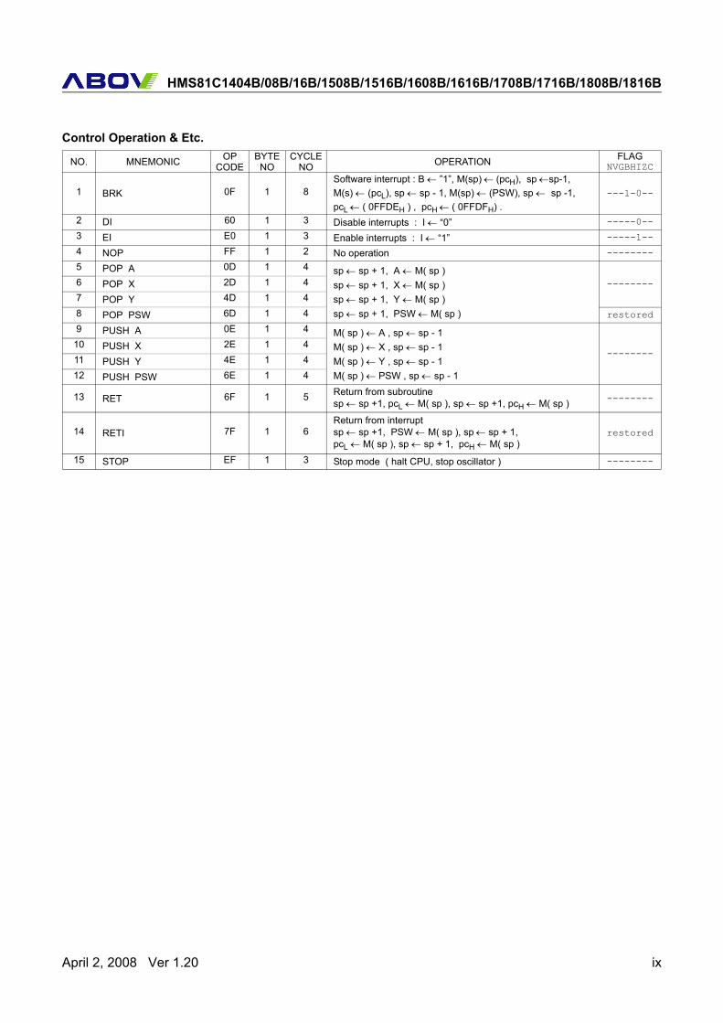
HMS81C1404B/08B/16B/1508B/1516B/1608B/1616B/1708B/1716B/1808B/1816B
Control Operation & Etc.
NO. MNEMONIC OPCODE
BYTENO
CYCLENO OPERATION FLAG
NVGBHIZC
1 BRK 0F 1 8Software interrupt : B ← ”1”, M(sp) ← (pcH), sp ←sp-1, M(s) ← (pcL), sp ← sp - 1, M(sp) ← (PSW), sp ← sp -1,pcL ← ( 0FFDEH ) , pcH ← ( 0FFDFH) .
---1-0--
2 DI 60 1 3 Disable interrupts : I ← “0” -----0--
3 EI E0 1 3 Enable interrupts : I ← “1” -----1--
4 NOP FF 1 2 No operation --------
5 POP A 0D 1 4 sp ← sp + 1, A ← M( sp )sp ← sp + 1, X ← M( sp )sp ← sp + 1, Y ← M( sp )sp ← sp + 1, PSW ← M( sp )
--------6 POP X 2D 1 47 POP Y 4D 1 48 POP PSW 6D 1 4 restored
9 PUSH A 0E 1 4 M( sp ) ← A , sp ← sp - 1M( sp ) ← X , sp ← sp - 1M( sp ) ← Y , sp ← sp - 1M( sp ) ← PSW , sp ← sp - 1
--------10 PUSH X 2E 1 411 PUSH Y 4E 1 412 PUSH PSW 6E 1 4
13 RET 6F 1 5 Return from subroutinesp ← sp +1, pcL ← M( sp ), sp ← sp +1, pcH ← M( sp ) --------
14 RETI 7F 1 6Return from interruptsp ← sp +1, PSW ← M( sp ), sp ← sp + 1,pcL ← M( sp ), sp ← sp + 1, pcH ← M( sp )
restored
15 STOP EF 1 3 Stop mode ( halt CPU, stop oscillator ) --------
April 2, 2008 Ver 1.20 ix
B. MASK ORDER SHEET(HMS81C1404B)
MASK ORDER & VERIFICATION SHEETHMS81C1404B-HN
1. Customer Information
Company Name
2. Device Information
3. Marking Specification
4. Delivery Schedule
Customer Sample
DateYYYY MM DD
Risk OrderYYYY MM DD
Quantity ABOV Confirmation
Application
Order DateYYYY MM DD
Tel: Fax:
Name &Signature:
Package 28SKDIP 28SOP
HMS81C1404B-HNxxxYYWW KOREA
5. ROM Code Verification
Verification Date:YYYY MM DD
Approval Date:YYYY MM DD
Please confirm our verification data. I agree with your verification data and confirmyou to make mask set.
Check Sum:
Tel: Fax:Name &Signature:
Tel: Fax:
Name &Signature:
Set “00” inthis area
0000H
F000H
FFFFH.OTP file data
EFFFH
Mask Data File Name: ( .OTP)
(Please check mark into )#1 index mark
pcs
pcs
Check Sum: ( )
Customer should write inside thick line box.
This box is written after “5.Verification”.
OSC Opt. Crystal RC
OFP Use Yes No
Notice : Unused userROM area shouldbe filled with “00H”
ONP Use Yes No
40ns 80ns
Yes No
HFNC
IN_CLK
C. MASK ORDER SHEET(HMS81C1408B)
MASK ORDER & VERIFICATION SHEETHMS81C1408B-HN
1. Customer Information
Company Name
2. Device Information
3. Marking Specification
4. Delivery Schedule
Customer Sample
DateYYYY MM DD
Risk OrderYYYY MM DD
Quantity ABOV Confirmation
Application
Order DateYYYY MM DD
Tel: Fax:
Name &Signature:
Package 28SKDIP 28SOP
HMS81C1408B-HNxxxYYWW KOREA
5. ROM Code Verification
Verification Date:YYYY MM DD
Approval Date:YYYY MM DD
Please confirm our verification data. I agree with your verification data and confirmyou to make mask set.
Check Sum:
Tel: Fax:Name &Signature:
Tel: Fax:
Name &Signature:
Set “00” inthis area
0000H
E000H
FFFFH.OTP file data
DFFFH
Mask Data File Name: ( .OTP)
(Please check mark into )#1 index mark
pcs
pcs
Check Sum: ( )
Customer should write inside thick line box.
This box is written after “5.Verification”.
OSC Opt. Crystal RC
OFP Use Yes No
Notice : Unused userROM area shouldbe filled with “00H”
ONP Use Yes No
40ns 80ns
Yes No
HFNC
IN_CLK
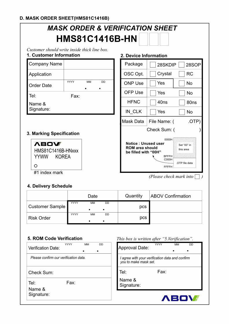
D. MASK ORDER SHEET(HMS81C1416B)
MASK ORDER & VERIFICATION SHEETHMS81C1416B-HN
1. Customer Information
Company Name
2. Device Information
3. Marking Specification
4. Delivery Schedule
Customer Sample
DateYYYY MM DD
Risk OrderYYYY MM DD
Quantity ABOV Confirmation
Application
Order DateYYYY MM DD
Tel: Fax:
Name &Signature:
Package 28SKDIP 28SOP
HMS81C1416B-HNxxxYYWW KOREA
5. ROM Code Verification
Verification Date:YYYY MM DD
Approval Date:YYYY MM DD
Please confirm our verification data. I agree with your verification data and confirmyou to make mask set.
Check Sum:
Tel: Fax:Name &Signature:
Tel: Fax:
Name &Signature:
Set “00” inthis area
0000H
C000H
FFFFH.OTP file data
BFFFH
Mask Data File Name: ( .OTP)
(Please check mark into )#1 index mark
pcs
pcs
Check Sum: ( )
Customer should write inside thick line box.
This box is written after “5.Verification”.
OSC Opt. Crystal RC
OFP Use Yes No
Notice : Unused userROM area shouldbe filled with “00H”
ONP Use Yes No
40ns 80ns
Yes No
HFNC
IN_CLK
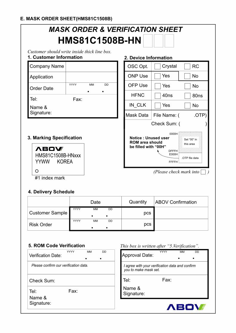
E. MASK ORDER SHEET(HMS81C1508B)
MASK ORDER & VERIFICATION SHEETHMS81C1508B-HN
1. Customer Information
Company Name
2. Device Information
3. Marking Specification
4. Delivery Schedule
Customer Sample
DateYYYY MM DD
Risk OrderYYYY MM DD
Quantity ABOV Confirmation
Application
Order DateYYYY MM DD
Tel: Fax:
Name &Signature:
HMS81C1508B-HNxxxYYWW KOREA
5. ROM Code Verification
Verification Date:YYYY MM DD
Approval Date:YYYY MM DD
Please confirm our verification data. I agree with your verification data and confirmyou to make mask set.
Check Sum:
Tel: Fax:Name &Signature:
Tel: Fax:
Name &Signature:
Set “00” inthis area
0000H
E000H
FFFFH.OTP file data
DFFFH
Mask Data File Name: ( .OTP)
(Please check mark into )#1 index mark
pcs
pcs
Check Sum: ( )
Customer should write inside thick line box.
This box is written after “5.Verification”.
OSC Opt. Crystal RC
OFP Use Yes No
Notice : Unused userROM area shouldbe filled with “00H”
ONP Use Yes No
40ns 80ns
Yes No
HFNC
IN_CLK

F. MASK ORDER SHEET(HMS81C1516B)
MASK ORDER & VERIFICATION SHEETHMS81C1516B-HN
1. Customer Information
Company Name
2. Device Information
3. Marking Specification
4. Delivery Schedule
Customer Sample
DateYYYY MM DD
Risk OrderYYYY MM DD
Quantity ABOV Confirmation
Application
Order DateYYYY MM DD
Tel: Fax:
Name &Signature:
HMS81C1516B-HNxxxYYWW KOREA
5. ROM Code Verification
Verification Date:YYYY MM DD
Approval Date:YYYY MM DD
Please confirm our verification data. I agree with your verification data and confirmyou to make mask set.
Check Sum:
Tel: Fax:Name &Signature:
Tel: Fax:
Name &Signature:
Set “00” inthis area
0000H
C000H
FFFFH.OTP file data
BFFFH
Mask Data File Name: ( .OTP)
(Please check mark into )#1 index mark
pcs
pcs
Check Sum: ( )
Customer should write inside thick line box.
This box is written after “5.Verification”.
OSC Opt. Crystal RC
OFP Use Yes No
Notice : Unused userROM area shouldbe filled with “00H”
ONP Use Yes No
40ns 80ns
Yes No
HFNC
IN_CLK

G. MASK ORDER SHEET(HMS81C1608B)
MASK ORDER & VERIFICATION SHEETHMS81C1608B-HN
1. Customer Information
Company Name
2. Device Information
3. Marking Specification
4. Delivery Schedule
Customer Sample
DateYYYY MM DD
Risk OrderYYYY MM DD
Quantity ABOV Confirmation
Application
Order DateYYYY MM DD
Tel: Fax:
Name &Signature:
HMS81C1608B-HNxxxYYWW KOREA
5. ROM Code Verification
Verification Date:YYYY MM DD
Approval Date:YYYY MM DD
Please confirm our verification data. I agree with your verification data and confirmyou to make mask set.
Check Sum:
Tel: Fax:Name &Signature:
Tel: Fax:
Name &Signature:
Set “00” inthis area
0000H
E000H
FFFFH.OTP file data
DFFFH
Mask Data File Name: ( .OTP)
(Please check mark into )#1 index mark
pcs
pcs
Check Sum: ( )
Customer should write inside thick line box.
This box is written after “5.Verification”.
OSC Opt. Crystal RC
OFP Use Yes No
Notice : Unused userROM area shouldbe filled with “00H”
ONP Use Yes No
40ns 80ns
Yes No
HFNC
IN_CLK
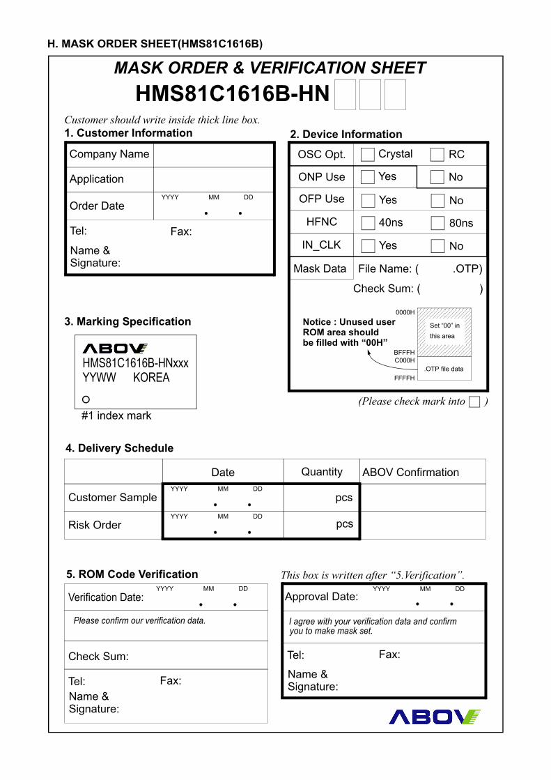
H. MASK ORDER SHEET(HMS81C1616B)
MASK ORDER & VERIFICATION SHEETHMS81C1616B-HN
1. Customer Information
Company Name
2. Device Information
3. Marking Specification
4. Delivery Schedule
Customer Sample
DateYYYY MM DD
Risk OrderYYYY MM DD
Quantity ABOV Confirmation
Application
Order DateYYYY MM DD
Tel: Fax:
Name &Signature:
HMS81C1616B-HNxxxYYWW KOREA
5. ROM Code Verification
Verification Date:YYYY MM DD
Approval Date:YYYY MM DD
Please confirm our verification data. I agree with your verification data and confirmyou to make mask set.
Check Sum:
Tel: Fax:Name &Signature:
Tel: Fax:
Name &Signature:
Set “00” inthis area
0000H
C000H
FFFFH.OTP file data
BFFFH
Mask Data File Name: ( .OTP)
(Please check mark into )#1 index mark
pcs
pcs
Check Sum: ( )
Customer should write inside thick line box.
This box is written after “5.Verification”.
OSC Opt. Crystal RC
OFP Use Yes No
Notice : Unused userROM area shouldbe filled with “00H”
ONP Use Yes No
40ns 80ns
Yes No
HFNC
IN_CLK
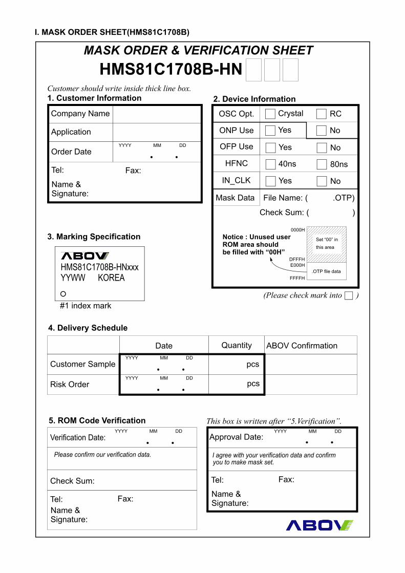
I. MASK ORDER SHEET(HMS81C1708B)
MASK ORDER & VERIFICATION SHEETHMS81C1708B-HN
1. Customer Information
Company Name
2. Device Information
3. Marking Specification
4. Delivery Schedule
Customer Sample
DateYYYY MM DD
Risk OrderYYYY MM DD
Quantity ABOV Confirmation
Application
Order DateYYYY MM DD
Tel: Fax:
Name &Signature:
HMS81C1708B-HNxxxYYWW KOREA
5. ROM Code Verification
Verification Date:YYYY MM DD
Approval Date:YYYY MM DD
Please confirm our verification data. I agree with your verification data and confirmyou to make mask set.
Check Sum:
Tel: Fax:Name &Signature:
Tel: Fax:
Name &Signature:
Set “00” inthis area
0000H
E000H
FFFFH.OTP file data
DFFFH
Mask Data File Name: ( .OTP)
(Please check mark into )#1 index mark
pcs
pcs
Check Sum: ( )
Customer should write inside thick line box.
This box is written after “5.Verification”.
OSC Opt. Crystal RC
OFP Use Yes No
Notice : Unused userROM area shouldbe filled with “00H”
ONP Use Yes No
40ns 80ns
Yes No
HFNC
IN_CLK

J. MASK ORDER SHEET(HMS81C1716B)
MASK ORDER & VERIFICATION SHEETHMS81C1716B-HN
1. Customer Information
Company Name
2. Device Information
3. Marking Specification
4. Delivery Schedule
Customer Sample
DateYYYY MM DD
Risk OrderYYYY MM DD
Quantity ABOV Confirmation
Application
Order DateYYYY MM DD
Tel: Fax:
Name &Signature:
HMS81C1716B-HNxxxYYWW KOREA
5. ROM Code Verification
Verification Date:YYYY MM DD
Approval Date:YYYY MM DD
Please confirm our verification data. I agree with your verification data and confirmyou to make mask set.
Check Sum:
Tel: Fax:Name &Signature:
Tel: Fax:
Name &Signature:
Set “00” inthis area
0000H
C000H
FFFFH.OTP file data
BFFFH
Mask Data File Name: ( .OTP)
(Please check mark into )#1 index mark
pcs
pcs
Check Sum: ( )
Customer should write inside thick line box.
This box is written after “5.Verification”.
OSC Opt. Crystal RC
OFP Use Yes No
Notice : Unused userROM area shouldbe filled with “00H”
ONP Use Yes No
40ns 80ns
Yes No
HFNC
IN_CLK

K. MASK ORDER SHEET(HMS81C1808B)
MASK ORDER & VERIFICATION SHEETHMS81C1808B-HN
1. Customer Information
Company Name
2. Device Information
3. Marking Specification
4. Delivery Schedule
Customer Sample
DateYYYY MM DD
Risk OrderYYYY MM DD
Quantity ABOV Confirmation
Application
Order DateYYYY MM DD
Tel: Fax:
Name &Signature:
HMS81C1808B-HNxxxYYWW KOREA
5. ROM Code Verification
Verification Date:YYYY MM DD
Approval Date:YYYY MM DD
Please confirm our verification data. I agree with your verification data and confirmyou to make mask set.
Check Sum:
Tel: Fax:Name &Signature:
Tel: Fax:
Name &Signature:
Set “00” inthis area
0000H
E000H
FFFFH.OTP file data
DFFFH
Mask Data File Name: ( .OTP)
(Please check mark into )#1 index mark
pcs
pcs
Check Sum: ( )
Customer should write inside thick line box.
This box is written after “5.Verification”.
OSC Opt. Crystal RC
OFP Use Yes No
Notice : Unused userROM area shouldbe filled with “00H”
ONP Use Yes No
40ns 80ns
Yes No
HFNC
IN_CLK
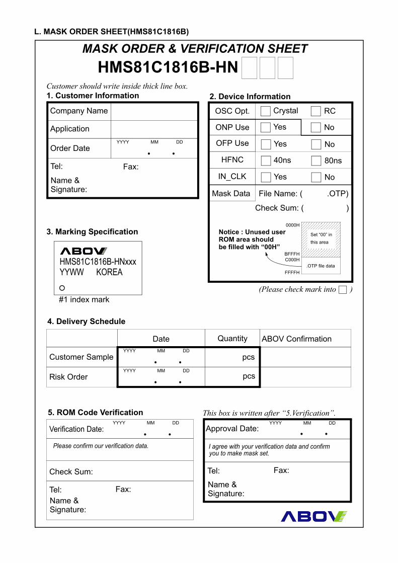
L. MASK ORDER SHEET(HMS81C1816B)
MASK ORDER & VERIFICATION SHEETHMS81C1816B-HN
1. Customer Information
Company Name
2. Device Information
3. Marking Specification
4. Delivery Schedule
Customer Sample
DateYYYY MM DD
Risk OrderYYYY MM DD
Quantity ABOV Confirmation
Application
Order DateYYYY MM DD
Tel: Fax:
Name &Signature:
HMS81C1816B-HNxxxYYWW KOREA
5. ROM Code Verification
Verification Date:YYYY MM DD
Approval Date:YYYY MM DD
Please confirm our verification data. I agree with your verification data and confirmyou to make mask set.
Check Sum:
Tel: Fax:Name &Signature:
Tel: Fax:
Name &Signature:
Set “00” inthis area
0000H
C000H
FFFFH.OTP file data
BFFFH
Mask Data File Name: ( .OTP)
(Please check mark into )#1 index mark
pcs
pcs
Check Sum: ( )
Customer should write inside thick line box.
This box is written after “5.Verification”.
OSC Opt. Crystal RC
OFP Use Yes No
Notice : Unused userROM area shouldbe filled with “00H”
ONP Use Yes No
40ns 80ns
Yes No
HFNC
IN_CLK