high speed mezzanine card (hsmc) specification
TRANSCRIPT

High Speed Mezzanine Card (HSMC)
Specification
101 Innovation Drive San Jose, CA 95134 www.altera.com
Document Version: 1.7Document Date: June 2009

Copyright © 2009 Altera Corporation. All rights reserved. Altera, The Programmable Solutions Company, the stylized Altera logo, specific device des-ignations, and all other words and logos that are identified as trademarks and/or service marks are, unless noted otherwise, the trademarks and service marks of Altera Corporation in the U.S. and other countries. All other product or service names are the property of their respective holders. Al-tera products are protected under numerous U.S. and foreign patents and pending applications, maskwork rights, and copyrights. Altera warrants performance of its semiconductor products to current specifications in accordance with Altera's standard warranty, but reserves the right to make changes to any products and services at any time without notice. Altera assumes no responsibility or liability arising out of the ap-plication or use of any information, product, or service described herein except as expressly agreed to in writing by Altera Corporation. Altera customers are advised to obtain the latest version of device specifications before relying on any published in-formation and before placing orders for products or services.
DS-01001-1.7
ii Development Board Version 1.0.0 Altera Corporation HSMC Specification June 2009

Altera Corporation June 2009
Contents
Chapter 1. Introduction1.1 Overview ............................................................................................................................................1–1
1.1.1 Objectives .................................................................................................................................1–21.1.2 Scope .........................................................................................................................................1–2
1.2 Theory and Operation ..................................................................................................................... 1–21.2.1 Host Boards ..............................................................................................................................1–21.2.2 Mezzanine Cards .....................................................................................................................1–31.2.3 HSMC Connectors ...................................................................................................................1–31.2.4 HSMC Power ...........................................................................................................................1–31.2.5 HSMC Interconnect .................................................................................................................1–31.2.6 Name and Logo Usage ...........................................................................................................1–3
Chapter 2. Mechanical2.1 Overview.............................................................................................................................................2–12.2 Dimensions ....................................................................................................................................... 2–12.3 HSMC Connector ............................................................................................................................. 2–1
2.3.1 ASP-122952-01 Header (Mezzanine Cards) .........................................................................2–22.3.2 ASP-122953-01 Socket (Host Boards) ...................................................................................2–5
2.4 Host Board Layout .......................................................................................................................... 2–82.5 Mezzanine Card Layout ................................................................................................................. 2–9
Chapter 3. Electrical3.1 Overview.............................................................................................................................................3–13.2 Board Classes ................................................................................................................................... 3–13.3 Signal Classes ................................................................................................................................... 3–2
3.3.1 Signal/Pin Naming Conventions .........................................................................................3–23.3.2 Signal/Pin Numbering Conventions ...................................................................................3–23.3.3 Signal/Pin Direction Conventions .......................................................................................3–23.3.4 Signal/Pin Definitions ............................................................................................................3–3
3.3.4.1 Transceiver .......................................................................................................................3–33.3.4.2 CMOS/LVDS ...................................................................................................................3–43.3.4.3 CMOS ................................................................................................................................3–63.3.4.4 CMOS CLK ......................................................................................................................3–73.3.4.5 CMOS/LVDS CLK .........................................................................................................3–83.3.4.6 JTAG/CMOS .................................................................................................................3–103.3.4.7 SMBUS/CMOS ..............................................................................................................3–103.3.4.8 PSNTn .............................................................................................................................3–10
3.4 Signaling Levels ............................................................................................................................. 3–113.5 Trace Impedance ............................................................................................................................ 3–123.6 Trace Lengths ................................................................................................................................. 3–133.7 Cross Talk ....................................................................................................................................... 3–13
iii Preliminary

Contents
3.8 Power ............................................................................................................................................... 3–143.8.1 Connector Current Capability .............................................................................................3–143.8.2 Power Pinout ..........................................................................................................................3–16
Chapter 4. Pinouts4.1 Overview.............................................................................................................................................4–14.2 Standard Host Pinouts .................................................................................................................... 4–1
4.2.1 Standard Single-Ended Host Pinout ....................................................................................4–14.2.2 Standard Differential Host Pinout ........................................................................................4–4
Chapter 5. Cables5.1 Overview.............................................................................................................................................5–15.2 Ribbon Cables ................................................................................................................................... 5–1
5.2.1 Web-based Configuration ......................................................................................................5–25.2.2 Host-to-Host Example ............................................................................................................5–45.2.3 Special Considerations ...........................................................................................................5–6
5.3 SMA Breakout Cables ..................................................................................................................... 5–6
Chapter 6. Signal Integrity6.1 Overview.............................................................................................................................................6–16.2 Performance ...................................................................................................................................... 6–1
6.2.1 Insertion Loss ...........................................................................................................................6–16.3 Guidelines ......................................................................................................................................... 6–2
6.3.1 LVDS / CMOS Signals ...........................................................................................................6–26.3.2 Transceiver Signals .................................................................................................................6–26.3.3 Differential Via ........................................................................................................................6–36.3.4 A/C Coupling Capacitors ......................................................................................................6–46.3.5 Surface Mount Pads ................................................................................................................6–5
Appendix A. Example Pinout MappingsIntroduction ............................................................................................................................................ A-1AMC Pinout ............................................................................................................................................ A-1PCI Express x8 Pinout ........................................................................................................................... A-4SPI4.2 Pinout .......................................................................................................................................... A-6CX-4 10G Ethernet Pinout .................................................................................................................... A-9Altera Daughter Card Pinout ............................................................................................................. A-12
Appendix B. GlossaryIntroduction ............................................................................................................................................. B-1
Additional InformationRevision History ................................................................................................................................ Info–iHow to Contact Altera .................................................................................................................... Info–iiiTypographic Conventions .............................................................................................................. Info–iii
iv Altera Corporation Preliminary June 2009

Altera Corporation June 2009
1. Introduction
1.1 OverviewThe Altera High Speed Mezzanine Card (HSMC) specification defines the electrical and mechanical properties of a high speed mezzanine card adapter interface for FPGA-based motherboards. This specification should allow for the design of interoperable motherboards and add-on cards by different manufacturers that can interoperate and utilize the high-performance I/O features found in today’s FPGA devices.
The connector is based on the Samtec 0.5 mm pitch, surface-mount QTH/QSH family of connectors. Compatible versions with this specification vary from 132 to 192 physical pins. The highest frequency signals are the clock-data-recovery differential signals found in bank 1. Signals between the host board FPGA device and HSMC connector are intended to be D/C coupled. Bank 1 also has dedicated JTAG, a system management bus (SMBus), and clock signals. The main CMOS/LVDS interface signals, including LVDS/CMOS clocks, are found in banks 2 and 3. Both 12-V and 3.3-V power pins are also found in banks 2 and 3.
Figure 1–1. Signal Bank Diagram
1–1 Preliminary

Theory and Operation
1.1.1 ObjectivesThe objective of this interface is to allow for multi-gigahertz differential signaling as well as slower single-ended signaling on most pins. The proper I/O connections can be programmed into the FPGA-based motherboard as required. The connector used is both low-cost and high performance. The layout requirements do not require significant motherboard space and allow for cabling options to support host-to-host connections.
The main data bus signals should allow for a mix of single-ended applications as well as source-synchronous and clock-data-recovery based differential signaling. Several other standard bus interfaces are presented through the connector including JTAG, SMBus, and dedicated clock inputs and outputs.
1.1.2 ScopeThis HSMC specification does not define specific interconnect usage, although it is optimized for current and emerging High-Speed Serial Interconnect standards such as PCI Express, Gigabit Ethernet, AMC, SPI4.2, and others.
A mapping of several popular bus standards is provided so that a host board and mezzanine card could be developed to support such standards. It is recognized that one may not be able to develop a single host to support every known standard. Instead, it should be made possible to support at least one, if not many, of the shown I/O signal mappings.
1.2 Theory and OperationThe HSMC interface provides a mechanism to extend the peripheral-set of an FPGA host board by means of a mezzanine card, which can address today’s high speed signaling requirement as well as standard or legacy low-speed device interface support. The mounting holes available on the mezzanine cards as well as the host boards provide mechanical support to the mezzanine card installed on the host board.
1.2.1 Host BoardsHost boards are defined as any board with an FPGA connected to one or more HSMC interfaces. Since FPGAs are configurable devices, the interconnect I/Os available on the HSMC connector can have all possible I/O standard and logic features that can be supported by the host FPGA, but usually they are limited by the wiring on the board, for instance, voltage referenced I/Os, single-ended (bidirectional) I/Os, differential (unidirectional) I/Os, and others.
1–2 Altera Corporation HSMC Specification June 2009

Introduction
1.2.2 Mezzanine CardsMezzanine cards are daughter cards which feature electrical components and interfaces or both. Mezzanine cards may come in several different sizes, interfaces and IO standard support, but all share some common attributes. When installed onto a host board, a mezzanine card is oriented parallel to the host board PCB plane and installed onto the HSMC connector.
1.2.3 HSMC ConnectorsHSMC connectors provide the interface between a host board and a mezzanine card. The ‘header’ part on a mezzanine card plugs into the ‘socket’ part on a host board. Various connector foot prints are allowed, but all HSMC connectors must adhere to the defined dimensional envelopes and electrical properties described in Chapter 2, Mechanical and Chapter 3, Electrical.
1.2.4 HSMC PowerThe host board provides +12 V DC and +3.3 V DC power to the mezzanine card through the HSMC connector. Any required voltage can be developed on the mezzanine card using appropriate power supply circuitry. Refer to “Power” on page 3–14 for more information.
1.2.5 HSMC InterconnectIn addition to power and clock signals, the host board provides access to JTAG, high speed serial I/O, and single-ended or differential I/O (as per mapping with the host board) through the HSMC connector. Chapter 4, Pinouts, describes the mapping of those signals to the HSMC connectors.
1.2.6 Name and Logo Usage
The logo shown above should be placed near the HSMC connector on host boards. To download the HSMC logo visit, ftp.altera.com/outgoing/hsmc_logo_fat.bmp.
Altera Corporation 1–3 June 2009 HSMC Specification

Altera Corporation June 2009
2. Mechanical
2.1 OverviewThis chapter defines the essential mechanical features and requirements for host boards and mezzanine cards. The following sections describes the HSMC connector, host boards and mezzanine cards.
2.2 DimensionsThe controlling dimensions are in inches unless stated otherwise. The unit for the dimensions shown in square brackets is mm unless stated otherwise. Periods are used as a decimal separator throughout this specification.
Tolerances are (unless stated otherwise):
Decimals:
.XX: ± .01 [.3]
.XXX: ± .005 [.13]
.XXXX: ±.0020 [.051]
Angle: 2°
2.3 HSMC ConnectorThe HSMC connector has a total of 172 pins, including 121 signal pins (120 signal pins + 1 PSNTn pin), 39 power pins, and 12 ground pins. The ground pins are much larger than the power pins and are located between the two rows of signal and power pins.
The connector is based on the 0.5 mm-pitch QSH/QTH family of high-speed board-to-board connectors from Samtec. There are three banks in this connector. Bank 1 will have every third pin removed as done in the QSH-DP/QTH-DP series. Bank 2 and Bank 3 have all of the pins populated as done in the QSH/QTH series. This configuration features 60 differential channels, or 120 single-ended I/O pins, plus special 12 V, 3.3 V, and GND plane connections with a vertical plane within the
2–1 Preliminary

Mechanical
connector that isolates the two rows of pins with 4 pins per bank. There are several connectors that can be used, each having different advantages. For more information on compatible connectors refer to the tables in the subsequent sections.
Figure 2–1 illustrate the HSMC connectors for both host boards and mezzanine cards.
Figure 2–1. HSMC Connectors
The default stacking height, or board to board air gap, is 5 mm. Using the smallest stacking height gives better signal integrity.
2.3.1 ASP-122952-01 Header (Mezzanine Cards)The ASP-122952-01 header provides 160 total pins as well as 12 ground plane connection pins down the center. Bank 1 (containing pin 1) has 40 pins (every third pin removed). Banks 2 and 3 have 60 pins each as no pins are removed. This connector is similar to the QTH family except for the bank 1 pin de-population is as found in the QTH-DP family. Optionally, you can use either the QTH or QTH-DP family connectors in the proper 3-bank versions knowing that the QTH-DP version will not carry power and the QTH will have slightly worse signal integrity on the transceiver pins. Refer to Table 2–1 for more details about the compatible connectors.
The header (ASP122952-01) is found on mezzanine cards. Figure 2–2 shows a top view of the connector. Bank 1 is denoted as a DP Bank which indicates that every third pin in this bank is removed.
Host boards provide transceivers to bank 1 and single-ended signals to banks 2 and 3. Typically, the single-ended signals are capable of differential signaling such as LVDS.
Samtec ASP-122952-01Mezzanine Card Connector
Samtec ASP-122953-01HSMC Host Board Connector
Vertical GND Plane
Vertical GND Plane
Bank 1
Bank 2
Bank 3
Altera Corporation 2–2 June 2009 HSMC Specification

HSMC Connector
Figure 2–2. Top View of the Samtec ASP-122952-01
Table 2–1 below shows several compatible models of connectors from Samtec. All of these models can use the same physical footprint.
Table 2–1. Mezzanine Header Compatibility
Part Number Description
ASP-122952-01 Recommended connector for mezzanine cards. This is a customized version of the QTH family connectors with 3 banks. Bank 1 is differential only (-DP) and banks 2 and 3 are like a normal QTH. This connector has 172 physical pins.
QTH-090-01-L-D-A QTH family connector with three banks. The difference between this connector and the ASP version is that all pins are populated in bank 1 of the connector. This difference equates to slightly lower signal integrity in that bank which typically carries multi-GHz clock-data-recovery signals. It is recommended that you do not leave the undefined pins in bank 1 floating; ground them or tie them to power. This connector has 192 physical pins.
QTH-060-01-L-D-DP-A QTH-DP family connector with three banks. The difference between this connector and the ASP version is that every third pin is removed in banks 2 and 3. These pins are connected to the 3.3 V and 12 V power signals. When these pins are in use, no power is delivered to the HSMC add-on card. LVDS/CMOS signals in banks 2 and 3 will have slightly better signal integrity. This connector has 132 physical pins.
2–3 Altera Corporation HSMC Specification June 2009

Mechanical
1 ASP-122952-01 is the recommended connector defined by the HSMC specification. If any of the compatible connectors from the above table is used, then the pin numbering will change accordingly due to different pin counts. Hence the example pinouts must be adjusted accordingly for the selected connector part.
Figure 2–3, Figure 2–4, and Figure 2–5 shows the front view, side section view, and PCB footprint of the Samtec ASP-122952-01.
Figure 2–3. Front View of the Samtec ASP-122952-01
Figure 2–4. Side Section View of the Samtec ASP-122952-01
Altera Corporation 2–4 June 2009 HSMC Specification

HSMC Connector
Figure 2–5. Footprint of the Samtec ASP-122952-01
f For more information about the ASP-122952-01 connector, visit Samtec’s website at http://www.samtec.com/signal_integrity/altera.aspx.
2.3.2 ASP-122953-01 Socket (Host Boards)The ASP-122953-01 socket provides 160 total pins as well as 12 ground plane connection pins down the center. Bank 1 (containing pin 1) has 40 pins (every third pin removed). Banks 2 and 3 have 60 pins each as no pins are removed. This connector is similar to the QSH family except for the bank 1 pin de-population is as found in the QSH-DP family. Optionally, one can use either the QSH or QSH-DP family connectors in the proper 3-bank versions knowing that the QSH-DP version will not carry power and the QSH will have slightly worse signal integrity on the transceiver pins. Refer to Table 2–2 for more details about the compatible connectors.
The socket (ASP122953-01) is found on host boards. Figure 2–6 shows the top view of this socket. Bank 1 is denoted as a DP Bank, meaning every third pin is removed.
As previously mentioned, host boards provide transceivers to bank 1 and single-ended signals to banks 2 and 3. Typically, the single-ended signals are capable of differential signaling as well (like LVDS, for example).
2–5 Altera Corporation HSMC Specification June 2009

Mechanical
Figure 2–6. Top View of the Samtec ASP-122953-01
Table 2–2 shows several compatible models of connectors from Samtec. All of these models can use the same physical footprint.
1 ASP-122953-01 is the recommended connector defined by the HSMC specification. If any of the compatible connectors from the above table is used, then the pin numbering will change accordingly due to different pin counts. Hence the example pinouts must be adjusted accordingly for the selected connector part.
Table 2–2. Host/Socket Compatibility
Part Number Description
ASP-122953-01 Recommended connector for host boards. This is a semi-custom version of the QSH family connectors with 3 banks. Bank 1 is differential only (-DP) and banks 2 and 3 are like a normal QSH. This connector has 172 physical pins.
QSH-090-01-L-D-A QSH family connector with three banks. The difference between this connector and the ASP version is that all pins are populated in bank 1 of the connector. This equates to slightly lower signal integrity in that bank which typically carries multi-GHz clock-data-recovery signals. It is recommended that you do not leave the undefined pins in bank 1 floating; ground them or tie them to power. This connector has 192 physical pins.
QSH-060-01-L-D-DP-A QSH-DP family connector with three banks. Difference between this connector and the ASP version is that every third pin is removed in banks 2 and 3. These pins connect to 3.3V and 12V power signals so the net result when using this pin is that no power will be delivered to the HSMC add-on card. LVDS/CMOS signals in banks 2 and 3 will have slightly better signal integrity. This connector has 132 physical pins.
Altera Corporation 2–6 June 2009 HSMC Specification
HSMC Connector
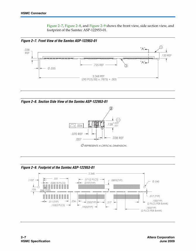
Figure 2–7, Figure 2–8, and Figure 2–9 shows the front view, side section view, and footprint of the Samtec ASP-122953-01.
Figure 2–7. Front View of the Samtec ASP-122953-01
Figure 2–8. Section Side View of the Samtec ASP-122953-01
Figure 2–9. Footprint of the Samtec ASP-122953-01
2–7 Altera Corporation HSMC Specification June 2009

Mechanical
f For more information about the ASP-122952-01 connector, visit Samtec’s website at http://www.samtec.com/signal_integrity/altera.aspx.
2.4 Host Board LayoutThe HSMC connector is to be located on the edge of the PCB to minimize the keepout area required on both host boards and mezzanine cards. The connector should be placed far enough from the board’s edge to allow for two mounting holes. This will ensure a rigid connection between the host board and mezzanine card. Figure 2–10 shows the dimensions of the keepout area and mounting holes.
Figure 2–10. Dimensions of Keep-Out Area and Mounting Holes
The connector should be placed far enough from the board’s edge to allow for two mounting holes, but in some cases this may not be possible. Figure 2–11 shows the dimensions of keepout area and mounting holes for a host board with room for only one mounting hole on each side.
PCB Edge0.69
8in.
0.13
5in.
Pin 1
0.125" hole, 0.250" pad
3.100in.
2.800in.0.150in.
Shaded area is aplacement keepout
on Host Board
0.92
3in.
Center Connectorbetween mounting holes
Altera Corporation 2–8 June 2009 HSMC Specification

Mezzanine Card Layout
Figure 2–11. Minimum Keep-Out Board Edge Layout
2.5 Mezzanine Card LayoutAs with the host board, the mezzanine card connector is to be placed on the edge of the PCB to minimize the keep-out area. The length of the HSMC is unimportant but the dimensions for the width and the mounting holes must be observed. Figure 2–12 shows the top view of mezzanine card.
3.100in.
2.800in.PCB Edge
Pin 1
0.22
5in.
0.150in.0.
451i
n.
Center Connectorbetween mounting holes
0.125" hole, 0.250" pad Shaded area is aplacement keepout
on Host Board
2–9 Altera Corporation HSMC Specification June 2009

Mechanical
Figure 2–12. Mezzanine Card Top View
Figure 2–13 shows the side view layout of mezzanine card.
Figure 2–13. Mezzanine Card Side View
3.076in.
2.800in.
ComponentSide Up Host PCB Edge
Board Size Grows This Way
0.138in.
0.69
8in.
0.13
5in.
0.92
3in.
Center Connectorbetween mounting holes
Mezzanine PCB
Host PCB
5mm
0.698in.
0923in.
Board SizeGrows This
Way
Altera Corporation 2–10 June 2009 HSMC Specification

Altera Corporation June 2009
3. Electrical
3.1 OverviewThis chapter defines the electrical properties of various signal groups in an HSMC interface as well as timing methodologies for data transfers.
3.2 Board ClassesFour classes of HSMC boards are defined within this specification to include low-cost platforms as well as high performance platforms. Table 3–1 shows the four HSMC board classes.
1 Type I, II, and III represents the host boards, while the Transceiver class is observed in mezzanine cards only.
A low-cost host may only support single-ended signals whereas a high-performance host may support programmable CMOS/LVDS or single-ended. A universal host adds clock-data recovery serializer/deserializer (SERDES). It is anticipated that other permutations of the above chart can exist but the three classes shown are the only ones defined herein.
The FPGA bank choices for I/O standards dictate how and which type of mezzanine card would be compatible with the host board (The I/O configuration on the host board usually determines which mezzanine cards will be supported by it and in what capacity). For example, if a mezzanine card with bidirectional single-ended
Table 3–1. HSMC Board Classes
Type HSMC Class
Bank 1 Bank 2 and Bank 3
CDR-based PCML SERDES
Source-Sync LVDS SERDES
Single-Ended CMOS Signals
I SE (1) — — vII SE (1) + LVDS — v vIII Universal v v vIV Transceiver v — —
Note:(1) SE is an abbreviation for single-ended signals
3–1 Preliminary

Electrical
I/O standard (for example, LVTTL/CMOS) is used with a host board having unidirectional I/O support (for example, LVDS), then the interface requirements must be observed to see the compatibility between the host and the mezzanine card. The reconfigurable FPGA may allow for using LVDS I/Os as single-ended I/Os, but voltage standard compatibility, dedicated I/O signal direction and availability of all I/Os must be observed to confirm the interoperability of the host board and the mezzanine card.
3.3 Signal ClassesThe HSMC interface defines eight classes of signals. These signal classes define the signaling type, or I/O standard, as well as assumptions on the way data is timed and clocked or both into transmitters and receivers.
1 Follow the standard differential host pinout for mezzanine cards that support a mix of LVDS and CMOS signals. This type of mezzanine cards contains four CMOS signals, 17 full-duplex differential channels (including two input and output clocks), and CLKIN0/CLKOUT0. Other perturbations may result in host board FPGA compilation errors due to I/O fitter rules such as single-ended and differential signal spacing.
3.3.1 Signal/Pin Naming ConventionsAll signals are active high unless denoted by a trailing n (negative) symbol. Differential signals are denoted by trailing p (positive) or n (negative) symbol.
3.3.2 Signal/Pin Numbering ConventionsAll the pinouts shown in this document are common to host boards as well as mezzanine cards. As the connector pin numbering on the HSMC header is mirrored for the HSMC socket, the pinout numbering remains the same for the HSMC header on the mezzanine card and connecting HSMC socket on the host board.
3.3.3 Signal/Pin Direction ConventionsSignal directions for transceivers as well as LVDS and other differential signals, or both are assumed to be unidirectional. Signal directions for CMOS are assumed to be bidirectional. Signal directions for clock input pins are assumed to be input only but may be bidirectional.
The signal naming conventions are relative to the host FPGA (from signal direction’s perspective). Hence care must be taken in the host and mezzanine card design when using unidirectional signals for transceivers, LVDS and other differential signals, or
Altera Corporation 3–2 June 2009 HSMC Specification

Signal Classes
both, especially for the differential and single-ended clock signals. If the direction specification (in or out) is not observed in the board design, it may render the mezzanine board unusable in the end host-daughter card system.
3.3.4 Signal/Pin DefinitionsThe following section describes signal/pin definitions for the HSMC specification.
3.3.4.1 Transceiver
Definition
The Transceiver class pins are intended to connect directly to PCML-compatible clock data- recovery SERDES pins for signaling of up to 6 Gbps or higher. These signals are always unidirectional and assume scrambling or encoding such that a clock can be recovered from the data stream. Run lengths and encoding or scrambling details are beyond the scope of this specification. This information needs to be documented on each host board and mezzanine card based on the device specifications.
Signal Direction
The signal direction naming conventions are relative to the host FPGA. For example, pin 1 (XCVR_TXp0) and pin 3 (XCVR_TXn0) should connect to transceiver output pins on a host board whereas pin 2 (XCVR_RXp0) and pin 4 (XCVR_RXn0) should connect to transceiver input pins on a host board.
Reduced Bus Widths
If a host cannot support eight transceiver channels due to limited channel counts then the lower bus numbers should be used. For example, if only four channels can be supplied to the HSMC connector, they would go to channels 0, 1, 2, and 3. If transceiver channels are not supported on a host then these pins should be left un-connected. Optionally, these pins can be connected to either CMOS/LVDS or CMOS class pins to extend the differential bus width to single-ended bus width to 112 signals (as shown in the generic single-ended/differential pinouts). It is considered a standard implementation to implement these pins as CMOS as host cards are encouraged to keep their pins limited to the standard 80 signal width with signals D80 through D111 being considered a special case. Host boards without Transceiver class pins should populate these only when many extra pins are available on the FPGA.
Coupling
All signals of this class must be DC-coupled on the host. Mezzanine card design can add A/C coupling as required but common-mode levels must be translated to HSMC compliant levels for this class of signal.
3–3 Altera Corporation HSMC Specification June 2009

Electrical
Termination
Receive signals require termination of 100 Ω differential. This termination should be on-die but board-level termination is acceptable.
Impedance
These traces must support 100 Ω differential impedances and can be routed as loosely coupled or tightly coupled (edge or broadside).
Layout Guidelines
Trace widths should be kept at or above 5 mils to reduce skin-effect losses and should reference a ground layer with no split plane crossings. These signals should be kept under 6 inches on a host if at all possible. Adherence to these simple guidelines, as well as those in the signal integrity section of this document will ensure the best performance and broadest compatibility with mezzanine cards of different types. Any traces designed to go over 1 Gbps should be simulated.
See Chapter 6, Signal Integrity for more details.
3.3.4.2 CMOS/LVDS
Definition
The CMOS/LVDS class pins are intended to connect directly to I/O pins on the host FPGA that can be configured either as LVDS-compatible differential pairs or LVTTL compatible single-ended I/O standards. The active I/O type can be programmed either by changing the FPGA configuration file or by modifying the signaling standard in-circuit.
Signal Directions
When programmed in single-ended mode on the host FPGA, these signals must support bidirectional operation. When programmed in differential mode, these signals are unidirectional with a naming convention to be based on the host. For example, pin 47 (LVDS_TXp0) and pin 49 (LVDS_TXn0) should connect to LVDS-compatible output pins whereas pin 48 (LVDS_RXp0) and pin 50 (LVDS_RXn0) should connect to LVDS compatible input pins.
Reduced Bus Widths
It is strongly suggested that host boards are designed to support the full specified bus widths. This interface is the main data bus portion of the HSMC specification and full support will guarantee inter-operability with the greatest number of mezzanine cards. If absolutely necessary due to pin limitations, signals should be populated starting at pin 41 and continue to the higher numbered signals. Note that pins 41, 42, 43, and 44 are intended to be single-ended only as described in the CMOS class section. These signals should be populated before those starting at pin 47 where signals become CMOS/LVDS class. Pins 41, 42, 43, and 44 are guaranteed
Altera Corporation 3–4 June 2009 HSMC Specification

Signal Classes
to operate at full speed concurrently with other host pins that are configured as differential. This configuration is important because designers of host boards must account for restrictions in I/O placement when both single-ended and differential pins are used. These rules are FPGA family and device specific but must be followed on any host board design to maintain the highest level of inter-operability with the greatest number of mezzanine cards. For pin numbers and data bus numbering, refer to “Standard Differential Host Pinout” on page 4–4.
Coupling
All signals of this class must be DC-coupled on the host. Mezzanine card design can add A/C coupling as required but common-mode levels must be translated to HSMC compliant levels for this class of signal.
Termination
Because these pins can be programmed to either differential or single-ended standards, the termination requirements require careful consideration.
For single-ended operation, it is ideal if the host FPGA supports driver strength control where 50-Ω output impedances can be selected. This output impedances will match the characteristic impedance of the traces themselves. For long trace lengths or heavy loads, drive strength could be increased as necessary until optimal signal integrity is achieved for the specific host board or mezzanine card combination. When impedance control is not possible, it is recommended to place series resistors on each line of a host board to allow for tuning through resistor value changes. Default resistors should be 0 Ω nominally since signal direction can not be assumed on a host board and higher values resistors found near a receiver can degrade signal integrity significantly. Programmable input termination is also ideally available so that a particular mezzanine card can be optimized but no input termination should be placed on a board or be permanently enabled on-die because signal direction is unknown on a generic host board.
For differential operation it is ideal if the host FPGA supports on-die 100 Ω differential termination between designated receiver pin pairs. For example, signals on a host that are connected to pin 48 (LVDS_RXp0) and pin 50 (LVDS_RXn0) must have the capability to allow for either on-die or on-board termination between the two pins, pin 47 (LVDS_TXp0) and pin 49 (LVDS_TXn0). This termination must be able to be disabled or removed to allow for less coupling when these pins are used as single-ended signals. For host boards which require to provide these as on-board resistors, it is recommended that they are not to be populated by default. It is anticipated that more mezzanine cards will use this class of pins in a single-ended configuration versus a differential configuration.
Impedance
These traces must have 50 Ω single-ended impedances and must be routed as loosely coupled pairs to minimize cross talk between p and n signals as they can also be used in a differential configuration.
3–5 Altera Corporation HSMC Specification June 2009

Electrical
Layout Guidelines
These signals should be matched in length to support high-speed source-synchronous connections. It is recommended that host boards match traces within 100 mils so that rise-times are not severely affected when the signals are operated as differential pairs. If a host board FPGA supports dynamic phase alignment (DPA) and does not require trace length matching, it is still recommended to match traces within 100 mils so that operation with mezzanine cards having devices which do not support this feature can still function. Trace widths can vary according to the stack up and intended frequency of operation or rise times.
See Chapter 6, Signal Integrity for more details.
3.3.4.3 CMOS
The CMOS class pins are intended to connect directly to pins that support LVTTL compatible single-ended I/O standards such as 3.3-V LVTTL/LVCMOS or 2.5-V LVTTL/LVCMOS.
Signal Directions
All CMOS class pins must support bidirectional operation.
Reduced Bus Widths
It is strongly suggested that host boards are designed to support the full 80-bit data bus width. This interface is the main interface for an HSMC for address, data, and control. Full support will guarantee inter-operability with the greatest number of mezzanine cards. If absolutely necessary due to pin limitations, signals should be populated starting at pin 41 and continue to the higher numbered signals. For pin numbers and data bus numbering, refer to “Standard Single-Ended Host Pinout” on page 4–1. For more information about the optional signals, D80 through D111, listed in the “Standard Single-Ended Host Pinout” section, refer to the Reduced Bus Width section in “Transceiver” on page 3–3.
Coupling
All signals of this class must be DC-coupled on the host. Mezzanine cards are assumed to be DC-coupled as well though there is no requirement.
Termination
It is ideal if the host FPGA supports driver strength control where 50 Ω output impedances can be selected. This output impedance will match the characteristic impedance of the traces themselves. For long trace lengths or heavy loads, drive strength could be increased as necessary until optimal signal integrity is achieved for the specific host board or mezzanine card combination. When impedance control is not possible, it is recommended to place series resistors on each line of a host board to allow for tuning through resistor value changes. Default resistors should be 0 Ω nominally since signal direction can not be assumed on a host board and
Altera Corporation 3–6 June 2009 HSMC Specification

Signal Classes
higher values resistors found near a receiver can degrade signal integrity significantly. Programmable input termination on the host FPGA is also ideally available so that a particular mezzanine card can be optimized but no input termination should be placed on a board or be permanently enabled on-die because signal direction is unknown on a generic host board.
Impedance
These traces must have 50 Ω single-ended impedances.
Layout Guidelines
These signals should be matched in length to support high-speed source-synchronous connections. It is recommended that host boards match traces within 250 mils to enable tight timing constraints to be achieved across a variety of mezzanine card timing requirements. Trace widths can vary according to the stack up and intended frequency of operation or rise times.
See Chapter 6, Signal Integrity for more details.
3.3.4.4 CMOS CLK
Definition
The CMOS CLK class pins are intended to connect directly to pins that support LVTTL compatible single-ended I/O standards such as 3.3-V LVTTL/LVCMOS or 2.5-V LVTTL/LVCMOS. These pins should also be operable as clocks in host FPGA devices relative to other signals in banks 2 and 3 of the “Standard Single-Ended Host Pinout” or “Standard Differential Host Pinout” sections. It is recommended to use dedicated clock pins on host FPGA devices even if any pin can be connected to FPGA clock networks. Any LVTTL-compatible pin can be used for output clocks as long as it can operate synchronously with the pins listed in the “Standard Single-Ended Host Pinout” or “Standard Differential Host Pinout” sections with a known static delay.
Signal Directions
Pin 40 (CLKIN0) must be connected to an input pin on the host FPGA. Pin 39 (CLKOUT0) must be connected to an output pin on the FPGA.
Reduced Bus Widths
Every host board must provide these two clock signals. These two pins are the recommended default clock signal pins for timing data transfers between host board FPGA devices and mezzanine cards for single-data-rate applications.
Coupling
All signals of this class must be DC-coupled on the host. Mezzanine cards are assumed to be DC-coupled as well though there is no requirement.
3–7 Altera Corporation HSMC Specification June 2009

Electrical
Termination
It is ideal if the host FPGA supports driver strength control where 50 Ω output impedances can be selected. This output impedances will match the characteristic impedance of the traces themselves. For long trace lengths or heavy loads, drive strength could be increased as necessary until optimal signal integrity is achieved for the specific host board/mezzanine card combination. When impedance control is not possible it is recommended to place series resistors on each line of a host board to allow for tuning through resistor value changes. Default resistor values should be calculated using simulations assuming worst-case trace lengths on the host board and 3 inches trace lengths on a mezzanine card.
Impedance
These traces must have 50 Ω single-ended impedances.
Layout Guidelines
These signals should match in length to the signals listed in the “Standard Single-Ended Host Pinout” or “Standard Differential Host Pinout” sections. It is recommended that host boards match traces within 250 mils to enable tight timing constraints to be achieved across a variety of mezzanine card timing requirements. Trace widths can vary according to the stack up and intended frequency of operation or rise times.
See Chapter 6, Signal Integrity for more details.
3.3.4.5 CMOS/LVDS CLK
Definition
The CMOS/LVDS CLK class pins are intended to connect directly to pins that support both either differential or LVTTL-compatible single-ended I/O standards such as 3.3-V LVTTL/LVCMOS or 2.5-V LVTTL/LVCMOS. If a host board FPGA cannot support the programmability of the input pins as either differential or single-ended then these pins should be connected as CMOS class pins. These pins should also be operable as clocks in host FPGA devices relative to other signals in banks 2 and 3 of the “Standard Single-Ended Host Pinout”or “Standard Differential Host Pinout” sections. It is recommended to use dedicated clock pins on host FPGA devices even if any pin can be connected to FPGA clock networks. Any LVTTL-compatible pin can be used for output clocks as long as it can operate synchronously with the pins listed in the “Standard Single-Ended Host Pinout” or “Standard Differential Host Pinout” sections with a known static delay.
1 Clock 2, found in bank 2 of the connector, is considered the primary clock of the two in or out pairs. If there is a limit on the number of dedicated clock input pins on a host FPGA, Clock 2 should be chosen over Clock 1 for these connections.
Altera Corporation 3–8 June 2009 HSMC Specification

Signal Classes
Signal Directions
When programmed in single-ended mode on the host FPGA, these signals must support bidirectional operation. When programmed in differential mode, these signals are unidirectional with a naming convention to be based on the host. For example, pin 95 (CLKOUT1p) and pin 97 (CLKOUT1n) should connect to LVDS-compatible output pins and pin 96 (CLKIN1p) and pin 98 (CLKIN1n) should connect to LVDS-compatible input pins.
Reduced Bus Widths
It is strongly suggested that host boards are designed to support the full 80-bit data bus width. This interface is the main interface for an HSMC for address, data, and control. Full support will guarantee inter-operability with the greatest number of mezzanine cards.
Coupling
All signals of this class must be DC-coupled on the host. Mezzanine cards are assumed to be DC-coupled as well though there is no requirement.
Termination
It is ideal if the host FPGA supports driver strength control where 50 Ω output impedances can be selected. This output impedances will match the characteristic impedance of the traces themselves. For long trace lengths or heavy loads, drive strength could be increased as necessary until optimal signal integrity is achieved for the specific host board or mezzanine card combination. When impedance control is not possible it is recommended to place series resistors on each line of a host board to allow for tuning through resistor value changes. Default resistors should be 0 Ω nominally since signal direction can not be assumed on a host board and higher values resistors found near a receiver can degrade signal integrity significantly. Programmable input termination on the host FPGA is also ideally available so that a particular mezzanine card can be optimized but no input termination should be placed on a board or be permanently enabled on-die because signal direction is unknown on a generic host board.
Impedance
These traces must have 50 Ω single-ended impedances.
Layout Guidelines
These signals should match in length to the signals listed in the “Standard Single-Ended Host Pinout” or “Standard Differential Host Pinout” sections. It is recommended that host boards match traces within 100 mils as are signals in the CMOS/LVDS pin class description. Trace widths can vary according to the stack up and intended frequency of operation or rise times.
See Chapter 6, Signal Integrity for more details.
3–9 Altera Corporation HSMC Specification June 2009

Electrical
3.3.4.6 JTAG/CMOS
The JTAG/CMOS signals are intended to connect to dedicated JTAG pins on the host FPGA and be part of the host FPGA device’s JTAG chain. If a host has multiple JTAG chains then the one that includes the host FPGA should also include the HSMC JTAG pins. A host must provide a switch or jumper to remove the HSMC from the chain if an installed HSMC does not have a JTAG chain or an HSMC is not installed. JTAG is assumed to be LVTTL-compatible. If the host has low-voltage pins on TDO then the signal must be up-converted to LVTTL-compatible levels. A host should be driving JTAG data to pin 38 and receiving JTAG data from pin 37.
Mezzanine card designs should connect TDI to TDO if JTAG-compatible devices are not present.
3.3.4.7 SMBUS/CMOS
The SMBUS/CMOS signals are intended to connect directly to LVTTL-compatible I/O pins on the host FPGA and to serial EEPROM device on a mezzanine card. For active mezzanine cards, the EEPROM device should contain information regarding the card that is installed. For passive adapters, the signals can optionally route through to compatible pins on the card being plugged into the HSMC adapter (for example, PCI Express has SMBUS pins).
3.3.4.8 PSNTn
The PSNTn pin is meant to drive an LED when the card is present, meaning correctly installed on a host. This signal should connect to GND on a mezzanine card design. A host should provide a single green LED near either pin 1 or pin 159 outside the host keep out area that is powered from an appropriate voltage such that, when an HSMC is inserted, the LED turns on with current flowing from the host through the
Table 3–2. JTAG Signals
Signal Name Description
JTAG TCK JTAG Clock — output from Host Board
JTAG TMS JTAG Mode Select — output from Host Board
JTAG TDI JTAG Data In — output from Host Board
JTAG TDO JTAG Data Out — input to Host Board
Table 3–3. SMBUS Signals
Signal Name Description
SCL Serial Clock — driven from host FPGA
SDA Serial Data — bidirectional data
Altera Corporation 3–10 June 2009 HSMC Specification

Signaling Levels
LED and resistor to pin 160 of the host Samtec socket to GND on pin 160 of the mezzanine card pin 160. A typical setup would use 3.3 V to an LED anode, an LED cathode to a current limiting resistor, to pin 160 of the Samtec socket on the host.
Figure 3–1. Mezzanine Card
3.4 Signaling LevelsThe HSMC interface supports three basic types of signaling standards: LVTTL, LVDS, and PCML. Host boards and mezzanine cards that claim to have HSMC-compliant interfaces do not have to support all three signal types but they must support at least one that is compatible.
In general, most single-ended 2.5-V and 3.3-V components are compatible using LVTTL levels. Table 3–4 shows the compatible signaling levels. LVDS pins may be able to drive other standards such as mini-LVDS or RSDS but the default operation should match with Table 3–4. Directions are relative to the host FPGA. Signal levels are taken at the connector. Some headroom has been added to industry standard levels for loss due to the host itself and unknown mezzanine card losses.
Table 3–4. Signaling Levels (Part 1 of 2)
Signal Type Parameter Minimum Maximum
LVTTL VCCIO 2.50 V (1) 3.30 V (1)
VIH 1.80 V VCCIO + 300 mV
VIL GND – 300 mV 0.90 V
VOH 2.00 V VCCIO
VOL GND 0.45 V
3–11 Altera Corporation HSMC Specification June 2009

Electrical
It is desirable for host boards to be able to support either LVDS or LVTTL-compatible single-ended signaling by reprogramming the FPGA. In this case one would typically choose a VCCIO level that accommodates both standards if possible. For example, Stratix II and Stratix III FPGA devices use 2.5-V power levels for LVDS signaling. These same devices can use 2.5 V or 3.3 V for LVTTL-compatible signaling levels in single-ended applications. The 2.5-V level should be chosen for the board because this supports both LVDS and the LVTTL-compatible 2.5-V CMOS standard.
Because overshoot and undershoot can be a greater concern for smaller process geometry devices in 65 nm and 40 nm, the designer needs to consider the acceptable overshoot to make sure device damage does not occur.
3.5 Trace ImpedanceAll traces are assumed to be 50 Ω single-ended traces. For LVDS or CMOS signals, the recommendation is to route those as loosely coupled meaning the traces are closer to the reference plane than they are to each other.
LVDS VID 200 mV 900 mV
VICM 200 mV 1800 mV
VOD 250 mV 450 mV
VOCM 1125 mV 1375 mV
VCCIO 2.50 V (1) 3.30 V (1)
RTERM 85 Ω 115 Ω
PCML VID 400 mV 2000 mV
VICM N/A (2) N/A (2)
VOD 500 mV 1200 mV
VOCM 300 mV 1000 mV
VCCI0 N/A N/A
RTERM 85 Ω 115 Ω
Notes to Table 3–4:(1) These values should be considered typical.(2) PCML interface assumes A/C-coupling. D/C-coupled applications need to be designed to
meet the HSMC host board’s FPGA actual common mode range.
Table 3–4. Signaling Levels (Part 2 of 2)
Signal Type Parameter Minimum Maximum
Altera Corporation 3–12 June 2009 HSMC Specification

Trace Lengths
3.6 Trace LengthsBoth maximum trace lengths and trace length matching need to be considered for both host boards and mezzanine cards. In general the host boards have the most stringent constraints and the mezzanine card can vary based on the application-specific constraints. These constraints vary by the signal type and board class. Table 3–5 shows the trace length matching.
3.7 Cross TalkThe allowable cross talk for this specification is 10% of the signal swing. For example, 3.3-V CMOS should be designed for 330 mV or less, and 2.5-V CMOS should be designed for 25 mV or less. These cross talk rules are enforced by setting up parallelism rules for PCB design.
Table 3–5. Trace Length Matching
Type Board Class Signal Type Constraint Value
I SE CMOS MAX Length 8000 mils
Length Matching ± 250 mils
II SE + LVDS CMOS/LVDS MAX Length 8000 mils
Length Matching ± 50 mils
P/N Length Matching ± 10 mils
III Universal CMOS/LVDS MAX Length 8000 mils
Length Matching ± 50 mils
P/N Length Matching ± 10 mils
PCML MAX Length 6000 mils
Length Matching ± 250 mils (1)
P/N Length Matching ± 5 mils
IV Transceiver PCML MAX Length 6000 mils
Length Matching ± 250 mils (1)
P/N Length Matching ± 5 mils
Note to Table 3–5:(1) Within a four-channel group such as XCVR_TX(7:4) or XCVR_TX(3:0).
3–13 Altera Corporation HSMC Specification June 2009

Electrical
The cross talk spacing rules shown in Table 3–6 reflect a PCB with a 4 mil plane to signal distance. If the stack up is different, the rules should be scaled accordingly using the Trace Spacing versus Reference Plane Distance column though simulation. This scaling is the only way to ensure compatibility with the cross-talk allowance.
3.8 PowerThe HSMC interface is designed such that it can carry well distributed +12 V, +3.3 V power and numerous GND lines. These power lines can be converted on the mezzanine card to any voltage required. The following sections provide detailed information about the power capability and power pinout.
3.8.1 Connector Current CapabilityThe power connections include 19 pins of 12 V and 20 pins of 3.3 V through Bank 2 and 3 respectively. The ground connection consists of 12 very wide center beams that are part of the Samtec QSH-DP connector’s center ground rail. The ground plane connections are rated at 7.8 A. Table 3–7 shows the ratings for these connections assuming the pinout in the following section. These numbers should be used as approximations. Actual ratings for the connections should be obtained from Samtec.
Table 3–6. Cross Talk Spacing Rules
Trace Spacing(Air Gap)
Parallel Trace Maximum Run Length
Trace Spacing versus Reference Plane Distance
4 mils < 500 mils 1× plane to trace
8 mils 500 to 1500 mils 2× plane to trace
12 mils >1500 mils 3× plane to trace
Table 3–7. Connector Current Capability (Part 1 of 2)
Bank Pin Class Voltage Pin Count Current Wattage
Bank 1 Signal 12 V 0 — —
3.3 V 0 — —
Plane GND 4 2.0 A / ea —
Bank 2 Signal 12 V 10 1.0 A / ea 120.0 W
3.3 V 10 1.0 A / ea 33 W
Plane GND 4 2.0 A / ea —
Altera Corporation 3–14 June 2009 HSMC Specification

Power
It is suggested that host boards are designed to provide the following minimum current levels to the connectors (see Table 3–8) in order to allow for broad support of various card and host designs. If possible, the current level supported can be placed on the board directly in silkscreen on a host.
If a host is unable to deliver the above listed power then it needs to be documented and some method of external powering should be provided using a jack or test point at a minimum. Mezzanine cards that exceed these levels should provide a similar jack or test point.
Bank 3 Signal 12 V 9 1.0 A / ea 108.0 W
3.3 V 10 1.0 A / ea 33 W
Plane GND 4 2.0 A / ea —
Total Signal 12 V 19 20 A 228.0 W
3.3 V 20 20 A 66.0 W
Plane GND 12 24 A —
Table 3–7. Connector Current Capability (Part 2 of 2)
Bank Pin Class Voltage Pin Count Current Wattage
Table 3–8. Recommended Host Power Delivery
Voltage Min Current from Host Min Wattage
12 V 1.0 A 12.0 W
3.3 V 2.0 A 6.6 W
Total 18.6 W per HSMC
3–15 Altera Corporation HSMC Specification June 2009

Electrical
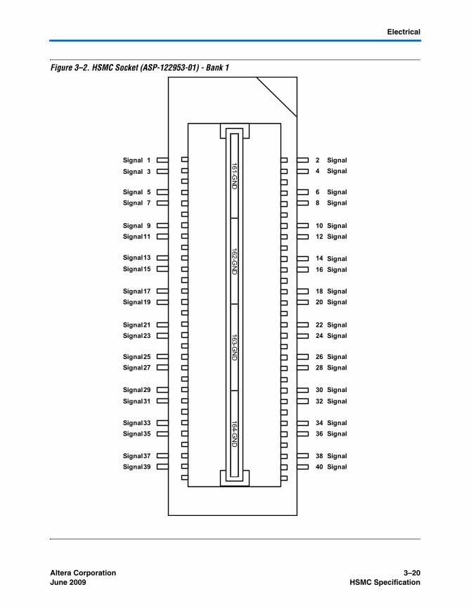
3.8.2 Power PinoutTable 3–9 shows the power pin positions within the HSMC connector. The center-rail ground plane connections (four per bank) are shown numbered at the end after the signal pin numbering is complete.
Table 3–9. Power Pin Positions within Samtec Connector (Part 1 of 4)
Pin Number Function Bank Number Function Pin Number
1 Signal
Bank 1
Signal 2
3 Signal Signal 4
5 Signal Signal 6
7 Signal Signal 8
9 Signal Signal 10
11 Signal Signal 12
13 Signal Signal 14
15 Signal Signal 16
17 Signal Signal 18
19 Signal Signal 20
21 Signal Signal 22
23 Signal Signal 24
25 Signal Signal 26
27 Signal Signal 28
29 Signal Signal 30
31 Signal Signal 32
33 Signal Signal 34
35 Signal Signal 36
37 Signal Signal 38
39 Signal Signal 40
Altera Corporation 3–16 June 2009 HSMC Specification

Power
41 Signal
Bank 2
Signal 42
43 Signal Signal 44
45 3.3 V 12 V 46
47 Signal Signal 48
49 Signal Signal 50
51 3.3 V 12 V 52
53 Signal Signal 54
55 Signal Signal 56
57 3.3 V 12 V 58
59 Signal Signal 60
61 Signal Signal 62
63 3.3 V 12 V 64
65 Signal Signal 66
67 Signal Signal 68
69 3.3 V 12 V 70
71 Signal Signal 72
73 Signal Signal 74
75 3.3 V 12 V 76
77 Signal Signal 78
79 Signal Signal 80
81 3.3 V 12 V 82
83 Signal Signal 84
85 Signal Signal 86
87 3.3 V 12 V 88
89 Signal Signal 90
91 Signal Signal 92
93 3.3 V 12 V 94
95 Signal Signal 96
97 Signal Signal 98
99 3.3 V 12 V 100
Table 3–9. Power Pin Positions within Samtec Connector (Part 2 of 4)
Pin Number Function Bank Number Function Pin Number
3–17 Altera Corporation HSMC Specification June 2009

Electrical
101 Signal
Bank 3
Signal 102
103 Signal Signal 104
105 3.3 V 12 V 106
107 Signal Signal 108
109 Signal Signal 110
111 3.3 V 12 V 112
113 Signal Signal 114
115 Signal Signal 116
117 3.3 V 12 V 118
119 Signal Signal 120
121 Signal Signal 122
123 3.3 V 12 V 124
125 Signal Signal 126
127 Signal Signal 128
129 3.3 V 12 V 130
131 Signal Signal 132
133 Signal Signal 134
135 3.3 V 12 V 136
137 Signal Signal 138
139 Signal Signal 140
141 3.3 V 12 V 142
143 Signal Signal 144
145 Signal Signal 146
147 3.3 V 12 V 148
149 Signal Signal 150
151 Signal Signal 152
153 3.3 V 12 V 154
155 Signal Signal 156
157 Signal Signal 158
159 3.3 V PSNTn (1) 160
161 Bank 1 GND Rail 1
162 Bank 1 GND Rail 2
163 Bank 1 GND Rail 3
164 Bank 1 GND Rail 4
Table 3–9. Power Pin Positions within Samtec Connector (Part 3 of 4)
Pin Number Function Bank Number Function Pin Number
Altera Corporation 3–18 June 2009 HSMC Specification

Power
Figure 3–2, Figure 3–3, and Figure 3–4 shows pin distribution for the HSMC socket (ASP-122953-01).
165 Bank 2 GND Rail 1
166 Bank 2 GND Rail 2
167 Bank 2 GND Rail 3
168 Bank 2 GND Rail 4
169 Bank 3 GND Rail 1
170 Bank 3 GND Rail 2
171 Bank 3 GND Rail 3
172 Bank 3 GND Rail 4
Note to Table 3–9:(1) PSNTn connects to GND on mezzanine card.
Table 3–9. Power Pin Positions within Samtec Connector (Part 4 of 4)
Pin Number Function Bank Number Function Pin Number
3–19 Altera Corporation HSMC Specification June 2009
Electrical
Figure 3–2. HSMC Socket (ASP-122953-01) - Bank 1
SignalSignal
SignalSignal
SignalSignal
SignalSignal
SignalSignal
SignalSignal
SignalSignal
SignalSignal
SignalSignal
SignalSignal
13
57
911
1315
1719
2123
2527
2931
3335
3739
SignalSignal
SignalSignal
SignalSignal
SignalSignal
SignalSignal
SignalSignal
SignalSignal
SignalSignal
SignalSignal
SignalSignal
24
68
1012
1416
1820
2224
2628
3032
3436
3840
161-GND
162-GND
163-GND
164-GND
Altera Corporation 3–20 June 2009 HSMC Specification

Power
Figure 3–3. HSMC Socket (ASP-122953-01) - Bank2
41
43
45
47
49
51
53
55
57
59
61
63
65
67
69
71
73
75
77
79
81
83
85
87
89
91
93
95
97
99
Signal
Signal
Signal
Signal
Signal
Signal
Signal
Signal
Signal
Signal
Signal
Signal
Signal
Signal
Signal
Signal
Signal
Signal
Signal
Signal
12V
12V
12V
12V
12V
12V
12V
12V
12V
12V
42
44
46
48
50
52
54
56
58
60
62
64
66
68
70
72
74
76
78
80
82
84
86
88
90
92
94
96
98
100
Signal
Signal
Signal
Signal
Signal
Signal
Signal
Signal
Signal
Signal
Signal
Signal
Signal
Signal
Signal
Signal
Signal
Signal
Signal
Signal
3.3V
3.3V
3.3V
3.3V
3.3V
3.3V
3.3V
3.3V
3.3V
3.3V
165-GN
D166-G
ND
167-GN
D168-G
ND
3–21 Altera Corporation HSMC Specification June 2009

Electrical
Figure 3–4. HSMC Socket (ASP-122953-01) - Bank3
Figure 3–5, Figure 3–6, and Figure 3–7 shows pin distribution for the mezzanine card header (ASP-122952-01).
101Signal103Signal1053.3V107Signal109Signal1113.3V113Signal115Signal1173.3V119Signal121Signal1233.3V125Signal127Signal1293.3V131Signal133Signal1353.3V137Signal139Signal1413.3V143Signal145Signal1473.3V149Signal151Signal1533.3V155Signal157Signal1593.3V
102 Signal104 Signal106 12V108 Signal110 Signal112 12V113 Signal116 Signal118 12V120 Signal122 Signal124 12V126 Signal128 Signal130 12V132 Signal134 Signal136 12V138 Signal140 Signal142 12V144 Signal146 Signal148 12V150 Signal152 Signal154 12V156 Signal158 Signal160 PSNTn
169-GND
170-GND
171-GND
172-GND
Altera Corporation 3–22 June 2009 HSMC Specification

Power
Figure 3–5. Mezzanine Card Header (ASP 122952-01) - Bank 1
Signal
Signal
Signal
Signal
Signal
Signal
Signal
Signal
Signal
Signal
Signal
Signal
Signal
Signal
Signal
Signal
Signal
Signal
Signal
Signal
1
3
5
7
9
11
13
15
17
19
21
23
25
27
29
31
33
35
37
39
Signal
Signal
Signal
Signal
Signal
Signal
Signal
Signal
Signal
Signal
Signal
Signal
Signal
Signal
Signal
Signal
Signal
Signal
Signal
Signal
2
4
6
8
10
12
14
16
18
20
22
24
26
28
30
32
34
36
38
40
161-
GN
D16
2-G
ND
163-
GN
D16
4-G
ND
3–23 Altera Corporation HSMC Specification June 2009

Electrical
Figure 3–6. Mezzanine Card Header (ASP-122952-01) - Bank 2
41
43
45
47
49
51
53
55
57
59
61
63
65
67
69
71
73
75
77
79
81
83
85
87
89
91
93
95
97
99
Signal
Signal
Signal
Signal
Signal
Signal
Signal
Signal
Signal
Signal
Signal
Signal
Signal
Signal
Signal
Signal
Signal
Signal
Signal
Signal
12V
12V
12V
12V
12V
12V
12V
12V
12V
12V
42
44
46
48
50
52
54
56
58
60
62
64
66
68
70
72
74
76
78
80
82
84
86
88
90
92
94
96
98
100
Signal
Signal
Signal
Signal
Signal
Signal
Signal
Signal
Signal
Signal
Signal
Signal
Signal
Signal
Signal
Signal
Signal
Signal
Signal
Signal
3.3V
3.3V
3.3V
3.3V
3.3V
3.3V
3.3V
3.3V
3.3V
3.3V
165-
GN
D16
6-G
ND
167-
GN
D16
8-G
ND
Altera Corporation 3–24 June 2009 HSMC Specification

Power
Figure 3–7. Mezzanine Card Header (ASP-122952-01) - Bank 3
101 Signal
103 Signal
105 3.3V
107 Signal
109 Signal
111 3.3V
113 Signal
115 Signal
117 3.3V
119 Signal
121 Signal
123 3.3V
125 Signal
127 Signal
129 3.3V
131 Signal
133 Signal
135 3.3V
137 Signal
139 Signal
141 3.3V
143 Signal
145 Signal
147 3.3V
149 Signal
151 Signal
153 3.3V
155 Signal
157 Signal
159 3.3V
102Signal
104Signal
10612V
108Signal
110Signal
11212V
113Signal
116Signal
11812V
120Signal
122Signal
12412V
126Signal
128Signal
13012V
132Signal
134Signal
13612V
138Signal
140Signal
14212V
144Signal
146Signal
14812V
150Signal
152Signal
15412V
156Signal
158Signal
160PSNTn
169-
GN
D17
0-G
ND
171-
GN
D17
2-G
ND
3–25 Altera Corporation HSMC Specification June 2009

Altera Corporation June 2009
4. Pinouts
4.1 OverviewThis chapter details the generic pinouts for use on host boards for both differential and single-ended standards, followed by recommended pinout mappings based on standard HSMC board classes.
4.2 Standard Host PinoutsThe following sections describe the intended generic pinouts both in physical location and electrical definition. The generic pin tables shown in the following sections are considered the standard pinout schemes for single-ended, differential, or both. Adhering to these pinouts allows a single host to use the maximum number of adapter cards. It is assumed that the LVDS pins double as CMOS per the host-board’s programming for Class II or Universal Class IV. This assumption requires the layout to use single-ended routing to minimize cross talk when single-ended applications are used.
4.2.1 Standard Single-Ended Host PinoutTable 4–1 lists the standard single-ended host pinout. This table represents Class I and Class II host boards and mezzanine cards.
Table 4–1. Standard Single-Ended Host Pinout (Part 1 of 4)
Pin Number Function Function Pin
Number Description
1 XCVR_TXp7 XCVR_RXp7 2 CMOS (1) (1)
3 XCVR_TXn7 XCVR_RXn7 4 CMOS (1) (1)
5 XCVR_TXp6 XCVR_RXp6 6 CMOS (1) (1)
7 XCVR_TXn6 XCVR_RXn6 8 CMOS (1) (1)
9 XCVR_TXp5 XCVR_RXp5 10 CMOS (1) (1)
11 XCVR_TXn5 XCVR_RXn5 12 CMOS (1) (1)
13 XCVR_TXp4 XCVR_RXp4 14 CMOS (1) (1)
15 XCVR_TXn4 XCVR_RXn4 16 CMOS (1) (1)
17 XCVR_TXp3 XCVR_RXp3 18 CMOS (1) (1)
4–1 Preliminary

Standard Host Pinouts
19 XCVR_TXn3 XCVR_RXn3 20 CMOS (1) (1)
21 XCVR_TXp2 XCVR_RXp2 22 CMOS (1) (1)
23 XCVR_TXn2 XCVR_RXn2 24 CMOS (1) (1)
25 XCVR_TXp1 XCVR_RXp1 26 CMOS (1) (1)
27 XCVR_TXn1 XCVR_RXn1 28 CMOS (1) (1)
29 XCVR_TXp0 XCVR_RXp0 30 CMOS (1) (1)
31 XCVR_TXn0 XCVR_RXn0 32 CMOS (1) (1)
33 SDA SCL 34 SMBUS/CMOS
35 JTAG_TCK JTAG_TMS 36 JTAG/CMOS
37 JTAG_TDO JTAG_TDI 38 JTAG/CMOS
39 CLKOUT0 CLKIN0 40 CMOS CLK
41 D0 D1 42 CMOS
43 D2 D3 44 CMOS
45 3.3 V 12 V 46 Power
47 D4 D5 48 CMOS
49 D6 D7 50 CMOS
51 3.3 V 12 V 52 Power
53 D8 D9 54 CMOS
55 D10 D11 56 CMOS
57 3.3 V 12 V 58 Power
59 D12 D13 60 CMOS
61 D14 D15 62 CMOS
63 3.3 V 12 V 64 Power
65 D16 D17 66 CMOS
67 D18 D19 68 CMOS
69 3.3 V 12 V 70 Power
71 D20 D21 72 CMOS
73 D22 D23 74 CMOS
75 3.3 V 12 V 76 Power
77 D24 D25 78 CMOS
79 D26 D27 80 CMOS
Table 4–1. Standard Single-Ended Host Pinout (Part 2 of 4)
Pin Number Function Function Pin
Number Description
4–2 Altera Corporation HSMC Specification June 2009

Pinouts
81 3.3 V 12 V 82 Power
83 D28 D29 84 CMOS
85 D30 D31 86 CMOS
87 3.3 V 12 V 88 Power
89 D32 D33 90 CMOS
91 D34 D35 92 CMOS
93 3.3 V 12 V 94 Power
95 D36 D37 96 LVDS CLKp/CMOS
97 D38 D39 98 LVDS CLKn/CMOS
99 3.3 V 12 V 100 Power
101 D40 D41 102 CMOS
103 D42 D43 104 CMOS
105 3.3 V 12 V 106 Power
107 D44 D45 108 CMOS
109 D46 D47 110 CMOS
111 3.3 V 12 V 112 Power
113 D48 D49 114 CMOS
115 D50 D51 116 CMOS
117 3.3 V 12 V 118 Power
119 D52 D53 120 CMOS
121 D54 D55 122 CMOS
123 3.3 V 12 V 124 Power
125 D56 D57 126 CMOS
127 D58 D59 128 CMOS
129 3.3 V 12 V 130 Power
131 D60 D61 132 CMOS
133 D62 D63 134 CMOS
135 3.3 V 12 V 136 Power
137 D64 D65 138 CMOS
139 D66 D67 140 CMOS
141 3.3 V 12 V 142 Power
143 D68 D69 144 CMOS
Table 4–1. Standard Single-Ended Host Pinout (Part 3 of 4)
Pin Number Function Function Pin
Number Description
Altera Corporation 4–3 June 2009 HSMC Specification

Standard Host Pinouts
4.2.2 Standard Differential Host PinoutTable 4–2 lists the standard differential host pinout.
145 D70 D71 146 CMOS
147 3.3 V 12 V 148 Power
149 D72 D73 150 CMOS
151 D74 D75 152 CMOS
153 3.3 V 12 V 154 Power
155 D76 D77 156 LVDS CLKp/CMOS
157 D78 D79 158 LVDS CLKn/CMOS
159 3.3 V PSNTn(2) 160 Power/PSNTn (2)
Notes to Table 4–1:(1) Use of these signals for CMOS is considered outside the scope of this specification as these pins
are intended for transceivers, which typically can neither drive CMOS levels or accept them as inputs. A mezzanine card that is designed to use these for CMOS should ensure that these pins can be tri-stated to NOT damage a potential Class III or Class IV transceiver-enabled board.
(2) PSNTn connects to GND on mezzanine card.
Table 4–1. Standard Single-Ended Host Pinout (Part 4 of 4)
Pin Number Function Function Pin
Number Description
Table 4–2. Standard Differential Host Pinout (Part 1 of 4)
Pin Number Function Function Pin
Number Description
1 XCVR_TXp7 XCVR_RXp7 2 Transceiver
3 XCVR_TXn7 XCVR_RXn7 4 Transceiver
5 XCVR_TXp6 XCVR_RXp6 6 Transceiver
7 XCVR_TXn6 XCVR_RXn6 8 Transceiver
9 XCVR_TXp5 XCVR_RXp5 10 Transceiver
11 XCVR_TXn5 XCVR_RXn5 12 Transceiver
13 XCVR_TXp4 XCVR_RXp4 14 Transceiver
15 XCVR_TXn4 XCVR_RXn4 16 Transceiver
17 XCVR_TXp3 XCVR_RXp3 18 Transceiver
19 XCVR_TXn3 XCVR_RXn3 20 Transceiver
21 XCVR_TXp2 XCVR_RXp2 22 Transceiver
4–4 Altera Corporation HSMC Specification June 2009

Pinouts
23 XCVR_TXn2 XCVR_RXn2 24 Transceiver
25 XCVR_TXp1 XCVR_RXp1 26 Transceiver
27 XCVR_TXn1 XCVR_RXn1 28 Transceiver
29 XCVR_TXp0 XCVR_RXp0 30 Transceiver
31 XCVR_TXn0 XCVR_RXn0 32 Transceiver
33 SDA SCL 34 SMBUS/CMOS
35 JTAG_TCK JTAG_TMS 36 JTAG/CMOS
37 JTAG_TDO JTAG_TDI 38 JTAG/CMOS
39 CLKOUT0 CLKIN0 40 CMOS CLK
41 D0 D1 42 CMOS
43 D2 D3 44 CMOS
45 3.3 V 12 V 46 Power
47 LVDS_TXp0 LVDS_RXp0 48 CMOS/LVDS
49 LVDS_TXn0 LVDS_RXn0 50 CMOS/LVDS
51 3.3 V 12 V 52 Power
53 LVDS_TXp1 LVDS_RXp1 54 CMOS/LVDS
55 LVDS_TXn1 LVDS_RXn1 56 CMOS/LVDS
57 3.3 V 12 V 58 Power
59 LVDS_TXp2 LVDS_RXp2 60 CMOS/LVDS
61 LVDS_TXn2 LVDS_RXn2 62 CMOS/LVDS
63 3.3 V 12 V 64 Power
65 LVDS_TXp3 LVDS_RXp3 66 CMOS/LVDS
67 LVDS_TXn3 LVDS_RXn3 68 CMOS/LVDS
69 3.3 V 12 V 70 Power
71 LVDS_TXp4 LVDS_RXp4 72 CMOS/LVDS
73 LVDS_TXn4 LVDS_RXn4 74 CMOS/LVDS
75 3.3 V 12 V 76 Power
77 LVDS_TXp5 LVDS_RXp5 78 CMOS/LVDS
79 LVDS_TXn5 LVDS_RXn5 80 CMOS/LVDS
81 3.3 V 12 V 82 Power
83 LVDS_TXp6 LVDS_RXp6 84 CMOS/LVDS
85 LVDS_TXn6 LVDS_RXn6 86 CMOS/LVDS
Table 4–2. Standard Differential Host Pinout (Part 2 of 4)
Pin Number Function Function Pin
Number Description
Altera Corporation 4–5 June 2009 HSMC Specification

Standard Host Pinouts
87 3.3 V 12 V 88 Power
89 LVDS_TXp7 LVDS_RXp7 90 CMOS/LVDS
91 LVDS_TXn7 LVDS_RXn7 92 CMOS/LVDS
93 3.3 V 12 V 94 Power
95 CLKOUT1p CLKIN1p 96 LVDS CLKp/CMOS
97 CLKOUT1n CLKIN1n 98 LVDS CLKn/CMOS
99 3.3 V 12 V 100 Power
101 LVDS_TXp8 LVDS_RXp8 102 CMOS/LVDS
103 LVDS_TXn8 LVDS_RXn8 104 CMOS/LVDS
105 3.3 V 12 V 106 Power
107 LVDS_TXp9 LVDS_RXp9 108 CMOS/LVDS
109 LVDS_TXn9 LVDS_RXn9 110 CMOS/LVDS
111 3.3 V 12 V 112 Power
113 LVDS_TXp10 LVDS_RXp10 114 CMOS/LVDS
115 LVDS_TXn10 LVDS_RXn10 116 CMOS/LVDS
117 3.3 V 12 V 118 Power
119 LVDS_TXp11 LVDS_RXp11 120 CMOS/LVDS
121 LVDS_TXn11 LVDS_RXn11 122 CMOS/LVDS
123 3.3 V 12 V 124 Power
125 LVDS_TXp12 LVDS_RXp12 126 CMOS/LVDS
127 LVDS_TXn12 LVDS_RXn12 128 CMOS/LVDS
129 3.3 V 12 V 130 Power
131 LVDS_TXp13 LVDS_RXp13 132 CMOS/LVDS
133 LVDS_TXn13 LVDS_RXn13 134 CMOS/LVDS
135 3.3 V 12 V 136 Power
137 LVDS_TXp14 LVDS_RXp14 138 CMOS/LVDS
139 LVDS_TXn14 LVDS_RXn14 140 CMOS/LVDS
141 3.3 V 12 V 142 Power
143 LVDS_TXp15 LVDS_RXp15 144 CMOS/LVDS
145 LVDS_TXn15 LVDS_RXn15 146 CMOS/LVDS
147 3.3 V 12 V 148 Power
149 LVDS_TXp16 LVDS_RXp16 150 CMOS/LVDS
Table 4–2. Standard Differential Host Pinout (Part 3 of 4)
Pin Number Function Function Pin
Number Description
4–6 Altera Corporation HSMC Specification June 2009

Pinouts
151 LVDS_TXn16 LVDS_RXn16 152 CMOS/LVDS
153 3.3 V 12 V 154 Power
155 CLKOUT2p CLKIN2p 156 LVDS CLKp/CMOS
157 CLKOUT2n CLKIN2n 158 LVDS CLKn/CMOS
159 3.3 V PSNTn(1) 160 Power/PSNTn(1)
Note to Table 4–2:(1) PSNTn connects to GND on mezzanine card.
Table 4–2. Standard Differential Host Pinout (Part 4 of 4)
Pin Number Function Function Pin
Number Description
Altera Corporation 4–7 June 2009 HSMC Specification

Altera Corporation June 2009
5. Cables
5.1 OverviewSeveral cabling options are available for the HSMC interface. Samtec offers a variety of off-the-shelf and custom cabling solutions compatible with this connector. The solutions include twin-ax, micro-coax, flex cable, ribbon, and SMA adapters for host-to-host, host to add-on card, and host to SMA or other connector configurations.
f See http://www.samtec.com/signal_integrity/altera.aspx for more information on cables.
5.2 Ribbon CablesSamtec offers off-the-shelf ribbon cable assemblies that allow for host-to-host connections as well as host-to-mezzanine-card connections (that is, extensions). These cables are available in both single-ended and differential configurations.
Figure 5–1. Data Rate Ribbon Cable
5–1 Preliminary

Cables
5.2.1 Web-based ConfigurationThe cable configurations can be customized using a web-based tool and ordered using a credit card or by using the correct part number and ordering direct. The screen shots below show some of the web pages in 2006. Contact Samtec for more information on how to order the cables.
Figure 5–2. Build a Data Rate Cable Assembly - Step 3
Altera Corporation 5–2 June 2009 HSMC Specification

Ribbon Cables
Figure 5–3. Build a Data Rate Cable Assembly - Step 5
5–3 Altera Corporation HSMC Specification June 2009

Cables
Figure 5–4. Build a Data Rate Cable Assembly - Step 7
After completing the steps, an exact datasheet is provided in PDF format that can be saved and can be ordered from http://www.samtec.com/signal_integrity/altera.aspx.
5.2.2 Host-to-Host ExampleFigure 5–5 shows an example of one of these cables. The end-points shown are called vertical launch in the SCREW OPTION page of the web tool. The pin 1 orientations shown are for a host-to-host configuration with a pin 1 to pin 2 mapping. You can connect two typical HSMC host Altera development kits together using this method.
Altera Corporation 5–4 June 2009 HSMC Specification

Ribbon Cables
Figure 5–5. Host-to-Host Cable
5–5 Altera Corporation HSMC Specification June 2009

Cables
Table 5–1 shows two popular options for cabling a host-to-host configuration and the manufacturer part numbers.
5.2.3 Special ConsiderationsFor a host-to-host configuration, the ribbon cable in the middle will actually need to twist as END NO. 1 is mounted to the opposite side as END NO. 2. Thus the cable must be physically long enough to allow for the twisting of three sets of twin-ax that are somewhat stiff. Also, three banks exist in the connector though the diagram shows only two. Note that JTAG and SMBus features will not work in most configurations as these pinouts are not as symmetrical as the data pins. Small modifications can enable this functionality. Power connections must be considered as the HSMC specification calls for power on the pins populated only on QTH/QSH family connectors and not on QTH-DP/QSH-DP family connectors. The recommended ASP connectors carry power as do the QTH/QSH family connectors.
5.3 SMA Breakout CablesAltera and Samtec designed a breakout cable for adapting a single bank of the 3-bank HSMC connector to SMA cables. Only the differential pins (pins found in the QSH-DP/QTH-DP) are used. Though fairly large and mechanically challenging, this cable offers the highest signal integrity and is the only completely flexible connection scheme by using SMA connectors.
Table 5–1. Host-to-Host Cable Part Numbers
Part Number Description
HQDP-060-06.00-TBR-TTL-2 6" Data Rate Cable, Host-to-Host (pin1-pin2), – DP different pairs only, 30 AWG twin-ax 100-Ω, –3 dB @ 1.92 GHz
HQDP-060-12.00-TBR-TTL-2 12" Data Rate Cable, Host-to-Host (pin1-pin2), – DP different pairs only, 30 AWG twin-ax 100-Ω, –3 dB @ 2.12 GHz
Altera Corporation 5–6 June 2009 HSMC Specification

SMA Breakout Cables
Figure 5–6. SMA Breakout Cable
Table 5–2 lists the SMA breakout cable part number description.
Table 5–2. SMA Breakout Cable Part Number
Part Number Description
HDR-128291-XX 12" RF Cable, – DP diff. pairs only, RG316, –3 dB @ ~ 3 GHz
5–7 Altera Corporation HSMC Specification June 2009

Altera Corporation June 2009
6. Signal Integrity
6.1 OverviewThe HSMC interface is designed to support very high data rates. Thus, signal integrity is an important topic. Careful layout will ensure that cards can interoperate successfully.
6.2 PerformanceThis section provides the performance data obtained for the HSMC interface.
6.2.1 Insertion LossThe preferred stacking height for a mezzanine card and a host board is a minimum 5 mm board-to-board. Using the smallest stacking height gives better high frequency performance.
Table 6–1 shows the insertion loss data for the various available stacking heights.
There are also some off-the-shelf micro-coax cables with good high speed performance that have been used by Altera for more than 1 Gbps applications at lengths of 6 inches. This same style of connector shows insertion loss data good enough (3 dB) for up to 6 inches cables at data rates of 3.125 Gbps. Samtec also offers flex-circuit cables that have even better high speed properties.
Table 6–1. Insertion Loss Data for the Various Stacking Heights
0, 50 mm QTH/QSH-DP Rated @ –3 dB Insertion Loss
5 mm Stack Height
Differential Pair Signaling 9.5 GHz / 19 Gbps
11 mm Stack Height
Differential Pair Signaling 6.0 GHz / 12 Gbps
16 mm Stack Height
Differential Pair Signaling 5.5 GHz / 11 Gbps
30 mm Stack Height
Differential Pair Signaling 7.0 GHz / 14 Gbps
6–1 Preliminary

Guidelines
6.3 GuidelinesThis section gives the guidelines for CMOS, LVDS and transceiver signals' interface on the HSMC connector.
6.3.1 LVDS / CMOS SignalsIn order to support an I/O standard of either LVDS or CMOS, one must design for high-speed on a host board. These signals are defined to operate up to 1.25 Gbps (625 MHz). The following rules should be applied to these signals in order to claim “full” compatibility with the LVDS and CMOS connections.
1. 50-Ω single-ended impedance target.
2. All traces must be matched to ± 50 mils.
3. Loosely coupled routing of P and N pairs must be used to minimize cross talk in single-ended systems.
a. Traces should be closer to the reference plane than each other.
4. All signals are to maintain a spacing that is based on its parallelism with other nets. The spacing is based on a ratio of signal to plane versus signal to signal (4 mil plane distance shown below).
a. 4 mils for parallel runs < 0.5 inches. (~1× spacing relative to plane distance)
b. 8 mils for parallel runs between 0.5 and 1.0 inches. (~2× spacing relative to plane distance)
c. 12 mils for parallel runs between 1.0 and 6.0 inches. (~3× spacing relative to plane distance)
5. Signals to have a maximum length of 8 inches on the host or the mezzanine card.
6.3.2 Transceiver SignalsThe HSMC interface is designed to support up to two XAUI interfaces and one SPI4.2 interface simultaneously. Future expansions of the HSMC may include 6.3 Gbps interface links. Careful attentions should be paid to the board material and board routing on both the host and mezzanine cards to avoid crosstalk and impedance discontinuities. Layout and routing design rules should include but not be limited to the following:
6–2 Altera Corporation HSMC Specification June 2009

Signal Integrity
■ High speed routes restricted to top, bottom, and bottom-most stripline or microstrip layers to minimize diff-via and connector pin stubs.
■ Diff-vias spread on .04 inches pitch.
■ Blocking caps use plane clearances (and signal keep-out) .03 inches deep surface mount lands should be referenced to a lower plane depending on land width.
■ Large antipads ovals around differential glutathione disulfide (GSSG) vias structures and anitpad.
■ Route all multi-gigabit signals on the top (or bottom) layer for at least short distance to allow room for GSSG differential vias.
■ Via placement should avoid “moating” which affects power delivery and ground reference.
■ Symmetrical routing into and out of transitions (vias, connector, BGAs, and so on).
■ Ground vias used at transitions to accommodate any common-mode signal.
■ 45° corners and jog-outs used to equalize lengths.
■ Differential pairs spaced to meet crosstalk constraints.
■ All positive (p) or negative (n) lengths between transitions matched.
6.3.3 Differential ViaThe most common transition is the differential via, or “diff-via” where you must transition from an upper stripline layer or top microstrip to a lower stripline layer or the bottom microstrip.
General design practices:
■ Use ~0.012 inches vias – larger if needed due to thicker board.
■ Use .022 inches pads (5 mil annular ring)
■ Use GSSG vias on .040 inches pitches.
■ Oblong antipads shown are roughly .055 inches × .095 inches (aligns with ground pad).
Altera Corporation 6–3 June 2009 HSMC Specification

Guidelines
■ If larger or smaller diameter vias are used, then scale all dimensions accordingly.
■ Remove annular rings on unrouted layers.
Figure 6–1. Differential Via structure
Every attempt to eliminate or reduce via stub lengths on via structures should be made. Techniques like routing from top microstrip to bottom microstrip, routing from top microstrip to the lowest available stripline should be used. If striplines on lower layers are not available then route to other striplines and consider back drilling via stubs. If design rules allow then use blind and buried via or both.
6.3.4 A/C Coupling CapacitorsUse DC blocking (AC coupling) capacitors if needed. These capacitors should be designed onto the mezzanine card to meet the application’s data rate and run length requirements.
General design practices:
■ Use 0402 differential caps on .050 inches spacing.
■ Plane clearances .110 inches wide and .120 inches high clearing all planes up to .030 inches depths.
■ Differential microstrip pairs are on (minimum of) .100 inches pitch and caps centered on these microstrips.
6–4 Altera Corporation HSMC Specification June 2009

Signal Integrity
■ Stagger capacitor pairs to reduce crosstalk.
■ Check the capacitor equivalent series inductance (ESL) to see if it is low enough for 6.5 Gbps operation.
■ Reference surface mount pads to a lower layer if possible.
■ Never route signals under plane cutouts.
■ Use ground vias for common mode return paths and electromagnetic interference (EMI) considerations.
Figure 6–2. Plane clearance and ground via arrangement to reduce EMI
6.3.5 Surface Mount PadsIn the HSMC interface, signals will encounter surface mount pads at that Samtec QSH and QTH connectors. Many times the traces attached to the surface mount pads are much thinner than the pads. For example, if a 100 Ω differential trace is 5 mils wide and are attached to a pair of pads that are 20 mils wide there will be an impedance drop at the pad. A cut out can be made on the plane layer just below the SMT pad. The pads can therefore be referenced to a lower plane that would be more appropriate for a 100 Ω differential signaling environment. Ground via should be placed close to the plane cut out so that common mode components of the signal are referenced to ground as well.
Altera Corporation 6–5 June 2009 HSMC Specification

Guidelines
Figure 6–3. Cut out underneath SMD Pads
6–6 Altera Corporation HSMC Specification June 2009

Altera Corporation DeveloJune 2009
Appendix A. Example Pinout Mappings
Introduction The examples below represent how one might map a standard bus format into one of the generic pinouts listed in the previous sections. The signal names reflect the naming conventions of the target bus being mapped. These pinouts are relative to the HSMC host.
AMC Pinout Table A–1 lists the pinout of AMC (single sided).
Table A–1. AMC (Single Sided) Pinout (Part 1 of 3)
Pin Number Function Function Pin Number Description
1 COMMON_TXp3 COMMON_RXp3 2 Transceiver
3 COMMON_TXn3 COMMON_RXn3 4 Transceiver
5 COMMON_TXp2 COMMON_RXp2 6 Transceiver
7 COMMON_TXn2 COMMON_RXn2 8 Transceiver
9 COMMON_TXp1 COMMON_RXp1 10 Transceiver
11 COMMON_TXn1 COMMON_RXn1 12 Transceiver
13 COMMON_TXp0 COMMON_RXp0 14 Transceiver
15 COMMON_TXn0 COMMON_RXn0 16 Transceiver
17 FATPIPES_TXp7 FATPIPES_RXp7 18 Transceiver
19 FATPIPES_TXn7 FATPIPES_RXn7 20 Transceiver
21 FATPIPES_TXp6 FATPIPES_RXp6 22 Transceiver
23 FATPIPES_TXn6 FATPIPES_RXn6 24 Transceiver
25 FATPIPES_TXp5 FATPIPES_RXp5 26 Transceiver
27 FATPIPES_TXn5 FATPIPES_RXn5 28 Transceiver
29 FATPIPES_TXp4 FATPIPES_RXp4 30 Transceiver
31 FATPIPES_TXn4 FATPIPES_RXn4 32 Transceiver
33 SDA SCL 34 SMBUS/CMOS
35 JTAG_TCK JTAG_TMS 36 JTAG/CMOS
37 JTAG_TDO JTAG_TDI 38 JTAG/CMOS
39 CLKOUT0 CLKIN0 40 CMOS CLK
41 ENABLEn PSn0 42 CMOS*
43 GA0 PSn1 44 CMOS*
pment Board Version 1.0. A–1 Preliminary

45 3.3 V 12 V 46 Power
47 GA1 GA2 48 CMOS
49 — — 50 —
51 3.3 V 12 V 52 Power
53 — — 54 —
55 — — 56 —
57 3.3 V 12 V 58 Power
59 — — 60 —
61 — — 62 —
63 3.3 V 12 V 64 Power
65 — — 66 —
67 — — 68 —
69 3.3 V 12 V 70 Power
71 — — 72 —
73 — — 74 —
75 3.3 V 12 V 76 Power
77 — — 78 —
79 — — 80 —
81 3.3 V 12 V 82 Power
83 — — 84 —
85 — — 86 —
87 3.3 V 12 V 88 Power
89 — — 90 —
91 — — 92 —
93 3.3 V 12 V 94 Power
95 CLKOUT1p CLKIN1p 96 LVDS CLKp/CMOS
97 CLKOUT1n CLKIN1n 98 LVDS CLKn/CMOS
99 3.3 V 12 V 100 Power
101 — — 102 —
103 — — 104 —
105 3.3 V 12 V 106 Power
107 — — 108 —
109 — — 110 —
Table A–1. AMC (Single Sided) Pinout (Part 2 of 3)
Pin Number Function Function Pin Number Description
A–2 Development Board Version 1.0. Altera Corporation HSMC Specification June 2009

111 3.3 V 12 V 112 Power
113 — — 114 —
115 — — 116 —
117 3.3 V 12 V 118 Power
119 — — 120 —
121 — — 122 —
123 3.3 V 12 V 124 Power
125 — — 126 —
127 — — 128 —
129 3.3 V 12 V 130 Power
131 — — 132 —
133 — — 134 —
135 3.3 V 12 V 136 Power
137 — — 138 —
139 — — 140 —
141 3.3 V 12V 142 Power
143 — — 144 —
145 — — 146 —
147 3.3 V 12 V 148 Power
149 — — 150 —
151 — — 152 —
153 3.3 V 12 V 154 Power
155 CLKOUT2p CLKIN2p 156 LVDS CLKp/CMOS
157 CLKOUT2n CLKIN2n 158 LVDS CLKn/CMOS
159 3.3 V PSNTn (1) 160 Power/PSNTn (1)
Note to Table A–1:(1) PSNTn connects to GND on mezzanine card.
Table A–1. AMC (Single Sided) Pinout (Part 3 of 3)
Pin Number Function Function Pin Number Description
Altera Corporation A–3 June 2009 HSMC Specification

PCI Express x8 Pinout
Table A–2 lists the pinout of PCI express x8.
Table A–2. PCI Express x8 Pinout (Part 1 of 3)
Pin Number Function Function Pin Number Description
1 PETp7 PERp7 2 Transceiver
3 PETn7 PERn7 4 Transceiver
5 PETp6 PERp6 6 Transceiver
7 PETn6 PERn6 8 Transceiver
9 PETp5 PERp5 10 Transceiver
11 PETn5 PERn5 12 Transceiver
13 PETp4 PERp4 14 Transceiver
15 PETn4 PERn4 16 Transceiver
17 PETp3 PERp3 18 Transceiver
19 PETn3 PERn3 20 Transceiver
21 PETp2 PERp2 22 Transceiver
23 PETn2 PERn2 24 Transceiver
25 PETp1 PERp1 26 Transceiver
27 PETn1 PERn1 28 Transceiver
29 PETp0 PERp0 30 Transceiver
31 PETn0 PERn0 32 Transceiver
33 SDA SCL 34 SMBUS/CMOS
35 JTAG_TCK JTAG_TMS 36 JTAG/CMOS
37 JTAG_TDO JTAG_TDI 38 JTAG/CMOS
39 — — 40 —
41 PRSNT# WAKE# 42 CMOS*
43 PERST# — 44 CMOS
45 3.3 V 12 V 46 Power
47 — — 48 —
49 — — 50 —
51 3.3 V 12 V 52 Power
53 — — 54 —
55 — — 56 —
57 3.3 V 12 V 58 Power
59 — — 60 —
A–4 Development Board Version 1.0. Altera Corporation HSMC Specification June 2009

61 — — 62 —
63 3.3 V 12 V 64 Power
65 - - 66 -
67 - - 68 -
69 3.3 V 12 V 70 Power
71 - - 72 -
73 - - 74 -
75 3.3 V 12 V 76 Power
77 - - 78 -
79 - - 80 -
81 3.3 V 12 V 82 Power
83 - - 84 -
85 - - 86 -
87 3.3 V 12 V 88 Power
89 - - 90 -
91 - - 92 -
93 3.3 V 12 V 94 Power
95 REFCLK_TXp REFCLK_RXp 96 LVDS CLKp / CMOS
97 REFCLK_TXn REFCLK_RXn 98 LVDS CLKn / CMOS
99 3.3 V 12 V 100 Power
101 - - 102 -
103 - - 104 -
105 3.3 V 12 V 106 Power
107 - - 108 -
109 - - 110 -
111 3.3 V 12 V 112 Power
113 - - 114 -
115 - - 116 -
117 3.3 V 12 V 118 Power
119 - - 120 -
121 - - 122 -
123 3.3 V 12 V 124 Power
125 - - 126 -
Table A–2. PCI Express x8 Pinout (Part 2 of 3)
Pin Number Function Function Pin Number Description
Altera Corporation A–5 June 2009 HSMC Specification

SPI4.2 Pinout Table A–3 lists the pinout of SPI4.2.
127 - - 128 -
129 3.3 V 12 V 130 Power
131 — — 132 —
133 — — 134 —
135 3.3 V 12 V 136 Power
137 — — 138 —
139 — — 140 —
141 3.3 V 12 V 142 Power
143 — — 144 —
145 — — 146 —
147 3.3 V 12 V 148 Power
149 — — 150 —
151 — — 152 —
153 3.3 V 12 V 154 Power
155 — — 156 —
157 — — 158 —
159 3.3 V PSNTn (1) 160 Power/PSNTn (1)
Note to Table A–2:(1) PSNTn connects to GND on mezzanine card.
Table A–2. PCI Express x8 Pinout (Part 3 of 3)
Pin Number Function Function Pin Number Description
Table A–3. SPI4.2 Pinout (Part 1 of 4)
Pin Number Function Function Pin Number Description
1 — — 2 —
3 — — 4 —
5 — — 6 —
7 — — 8 —
9 — — 10 —
11 — — 12 —
13 — — 14 —
15 — — 16 —
A–6 Development Board Version 1.0. Altera Corporation HSMC Specification June 2009

17 — — 18 —
19 — — 20 —
21 — — 22 —
23 — — 24 —
25 — — 26 —
27 — — 28 —
29 — — 30 —
31 — — 32 —
33 — — 34 —
35 — — 36 —
37 — — 38 —
39 RSCLK TSCLK 40 CMOS CLK
41 RDAT0 TDAT0 42 CMOS*
43 RDAT1 TDAT1 44 CMOS*
45 3.3 V 12 V 46 Power
47 SPI_TDATp0 SPI_RDATp0 48 LVDS
49 SPI_TDATn0 SPI_RDATn0 50 LVDS
51 3.3 V 12 V 52 Power
53 SPI_TDATp1 SPI_RDATp1 54 LVDS
55 SPI_TDATn1 SPI_RDATn1 56 LVDS
57 3.3 V 12 V 58 Power
59 SPI_TDATp2 SPI_RDATp2 60 LVDS
61 SPI_TDATn2 SPI_RDATn2 62 LVDS
63 3.3 V 12 V 64 Power
65 SPI_TDATp3 SPI_RDATp3 66 LVDS
67 SPI_TDATn3 SPI_RDATn3 68 LVDS
69 3.3 V 12 V 70 Power
71 SPI_TDATp4 SPI_RDATp4 72 LVDS
73 SPI_TDATn4 SPI_RDATn4 74 LVDS
75 3.3 V 12 V 76 Power
77 SPI_TDATp5 SPI_RDATp5 78 LVDS
79 SPI_TDATn5 SPI_RDATn5 80 LVDS
81 3.3 V 12 V 82 Power
Table A–3. SPI4.2 Pinout (Part 2 of 4)
Pin Number Function Function Pin Number Description
Altera Corporation A–7 June 2009 HSMC Specification

83 SPI_TDATp6 SPI_RDATp6 84 LVDS
85 SPI_TDATn6 SPI_RDATn6 86 LVDS
87 3.3 V 12 V 88 Power
89 SPI_TDATp7 SPI_RDATp7 90 LVDS
91 SPI_TDATn7 SPI_RDATn7 92 LVDS
93 3.3 V 12 V 94 Power
95 — — 96 —
97 — — 98 —
99 3.3 V 12 V 100 Power
101 SPI_TDATp8 SPI_RDATp8 102 LVDS
103 SPI_TDATn8 SPI_RDATn8 104 LVDS
105 3.3 V 12 V 106 Power
107 SPI_TDATp9 SPI_RDATp9 108 LVDS
109 SPI_TDATn9 SPI_RDATn9 110 LVDS
111 3.3 V 12 V 112 Power
113 SPI_TDATp10 SPI_RDATp10 114 LVDS
115 SPI_TDATn10 SPI_RDATn10 116 LVDS
117 3.3 V 12 V 118 Power
119 SPI_TDATp11 SPI_RDATp11 120 LVDS
121 SPI_TDATn11 SPI_RDATn11 122 LVDS
123 3.3 V 12 V 124 Power
125 SPI_TDATp12 SPI_RDATp12 126 LVDS
127 SPI_TDATn12 SPI_RDATn12 128 LVDS
129 3.3 V 12 V 130 Power
131 SPI_TDATp13 SPI_RDATp13 132 LVDS
133 SPI_TDATn13 SPI_RDATn13 134 LVDS
135 3.3 V 12 V 136 Power
137 SPI_TDATp14 SPI_RDATp14 138 LVDS
139 SPI_TDATn14 SPI_RDATn14 140 LVDS
141 3.3 V 12 V 142 Power
143 SPI_TDATp15 SPI_RDATp15 144 LVDS
145 SPI_TDATn15 SPI_RDATn15 146 LVDS
147 3.3 V 12 V 148 Power
Table A–3. SPI4.2 Pinout (Part 3 of 4)
Pin Number Function Function Pin Number Description
A–8 Development Board Version 1.0. Altera Corporation HSMC Specification June 2009

CX-4 10G Ethernet Pinout
Table A–4 lists the pinout of CX-4 10G Ethernet.
149 SPI_TCTLp SPI_RCTLp 150 LVDS
151 SPI_TCTLn SPI_RCTLn 152 LVDS
153 3.3 V 12 V 154 Power
155 SPI_TDCLKp SPI_RDCLKp 156 LVDS CLKp/CMOS
157 SPI_TDCLKn SPI_RDCLKn 158 LVDS CLKn/CMOS
159 3.3 V PSNTn 160 Power/PSNTn
Table A–3. SPI4.2 Pinout (Part 4 of 4)
Pin Number Function Function Pin Number Description
Table A–4. CX-4 10G Ethernet Pinout (Part 1 of 3)
Pin Number Function Function Pin Number Description
1 — — 2 —
3 — — 4 —
5 — — 6 —
7 — — 8 —
9 — — 10 —
11 — — 12 —
13 — — 14 —
15 — — 16 —
17 SLTXp3 - S10 DLRXp3 - S7 18 Transceiver
19 SLTXn3 - S9 DLRXn3 - S8 20 Transceiver
21 SLTXp2 - S12 DLRXp2 - S5 22 Transceiver
23 SLTXn2 - S11 DLRXn2 - S6 24 Transceiver
25 SLTXp1 - S14 DLRXp1 - S3 26 Transceiver
27 SLTXn1 - S13 DLRXn1 - S4 28 Transceiver
29 SLTXp0 - S16 DLRXp0 - S1 30 Transceiver
31 SLTXn0 - S15 DLRXn0 - S2 32 Transceiver
33 — — 34 —
35 — — 36 —
37 — — 38 —
39 — — 40 —
Altera Corporation A–9 June 2009 HSMC Specification

41 — — 42 —
43 — — 44 —
45 3.3 V 12 V 46 Power
47 — — 48 —
49 — — 50 —
51 3.3 V 12 V 52 Power
53 — — 54 —
55 — — 56 —
57 3.3 V 12 V 58 Power
59 — — 60 —
61 — — 62 —
63 3.3 V 12 V 64 Power
65 — — 66 —
67 — — 68 —
69 3.3 V 12 V 70 Power
71 — — 72 —
73 — — 74 —
75 3.3 V 12 V 76 Power
77 — — 78 —
79 — — 80 —
81 3.3 V 12 V 82 Power
83 — — 84 —
85 — — 86 —
87 3.3 V 12 V 88 Power
89 — — 90 —
91 — — 92 —
93 3.3 V 12 V 94 Power
95 — — 96 —
97 — — 98 —
99 3.3 V 12 V 100 Power
101 — — 102 —
103 — — 104 —
105 3.3 V 12 V 106 Power
Table A–4. CX-4 10G Ethernet Pinout (Part 2 of 3)
Pin Number Function Function Pin Number Description
A–10 Development Board Version 1.0. Altera Corporation HSMC Specification June 2009

107 — — 108 —
109 — — 110 —
111 3.3 V 12 V 112 Power
113 — — 114 —
115 — — 116 —
117 3.3 V 12 V 118 Power
119 — — 120 —
121 — — 122 —
123 3.3 V 12 V 124 Power
125 — — 126 —
127 — — 128 —
129 3.3 V 12 V 130 Power
131 — — 132 —
133 — — 134 —
135 3.3 V 12 V 136 Power
137 — — 138 —
139 — — 140 —
141 3.3 V 12 V 142 Power
143 — — 144 —
145 — — 146 —
147 3.3 V 12 V 148 Power
149 — — 150 —
151 — — 152 —
153 3.3 V 12 V 154 Power
155 — — 156 —
157 — — 158 —
159 3.3 V PSNTn (1) 160 Power/PSNTn (1)
Note to Table A–4:(1) PSNTn connects to GND on mezzanine card.
Table A–4. CX-4 10G Ethernet Pinout (Part 3 of 3)
Pin Number Function Function Pin Number Description
Altera Corporation A–11 June 2009 HSMC Specification

Altera Daughter Card Pinout
Table A–5 lists the pinouts of Altera Daughter Card (also known as Santa Cruz Card).
Table A–5. Altera Daughter Card (also known as Santa Cruz Card) Pinout (Part 1 of 3)
Pin Number Function Function Pin Number Description
1 — — 2 —
3 — — 4 —
5 — — 6 —
7 — — 8 —
9 — — 10 —
11 — — 12 —
13 — — 14 —
15 — — 16 —
17 — — 18 —
19 — — 20 —
21 — — 22 —
23 — — 24 —
25 — — 26 —
27 — — 28 —
29 — — 30 —
31 — — 32 —
33 — — 34 —
35 — — 36 —
37 — — 38 —
39 — — 40 —
41 PROTO1_D1 PROTO1_D0 42 CMOS
43 PROTO1_D3 PROTO1_D2 44 CMOS
45 3.3 V 12 V 46 Power
47 PROTO1_D5 PROTO1_D4 48 CMOS
49 PROTO1_D7 PROTO1_D6 50 CMOS
51 3.3 V 12 V 52 Power
53 PROTO1_D9 PROTO1_D8 54 CMOS
55 PROTO1_D11 PROTO1_D10 56 CMOS
57 3.3 V 12 V 58 Power
59 PROTO1_D13 PROTO1_D12 60 CMOS
A–12 Development Board Version 1.0. Altera Corporation HSMC Specification June 2009

61 PROTO1_D15 PROTO1_D14 62 CMOS
63 3.3 V 12 V 64 Power
65 PROTO1_D17 PROTO1_D16 66 CMOS
67 PROTO1_D19 PROTO1_D18 68 CMOS
69 3.3 V 12 V 70 Power
71 PROTO1_D21 PROTO1_D20 72 CMOS
73 PROTO1_D23 PROTO1_D22 74 CMOS
75 3.3 V 12 V 76 Power
77 PROTO1_D25 PROTO1_D24 78 CMOS
79 PROTO1_D27 PROTO1_D26 80 CMOS
81 3.3 V 12 V 82 Power
83 PROTO1_D29 PROTO1_D28 84 CMOS
85 PROTO1_D31 PROTO1_D30 86 CMOS
87 3.3 V 12 V 88 Power
89 PROTO1_D33 PROTO1_D32 90 CMOS
91 PROTO1_D35 PROTO1_D34 92 CMOS
93 3.3 V 12 V 94 Power
95 PROTO1_D37 PROTO1_D36 96 CMOS
97 PROTO1_D39 PROTO1_D38 98 CMOS
99 3.3 V 12 V 100 Power
101 PROTO2_D1 PROTO2_D0 102 CMOS
103 PROTO2_D3 PROTO2_D2 104 CMOS
105 3.3 V 12 V 106 Power
107 PROTO2_D5 PROTO2_D4 108 CMOS
109 PROTO2_D7 PROTO2_D6 110 CMOS
111 3.3 V 12 V 112 Power
113 PROTO2_D9 PROTO2_D8 114 CMOS
115 PROTO2_D11 PROTO2_D10 116 CMOS
117 3.3 V 12 V 118 Power
119 PROTO2_D13 PROTO2_D12 120 CMOS
121 PROTO2_D15 PROTO2_D14 122 CMOS
123 3.3 V 12 V 124 Power
125 PROTO2_D17 PROTO2_D16 126 CMOS
Table A–5. Altera Daughter Card (also known as Santa Cruz Card) Pinout (Part 2 of 3)
Pin Number Function Function Pin Number Description
Altera Corporation A–13 June 2009 HSMC Specification

127 PROTO2_D19 PROTO2_D18 128 CMOS
129 3.3 V 12 V 130 Power
131 PROTO2_D21 PROTO2_D20 132 CMOS
133 PROTO2_D23 PROTO2_D22 134 CMOS
135 3.3 V 12 V 136 Power
137 PROTO2_D25 PROTO2_D24 138 CMOS
139 PROTO2_D27 PROTO2_D26 140 CMOS
141 3.3 V 12 V 142 Power
143 PROTO2_D29 PROTO2_D28 144 CMOS
145 PROTO2_D31 PROTO2_D30 146 CMOS
147 3.3 V 12 V 148 Power
149 PROTO2_D33 PROTO2_D32 150 CMOS
151 PROTO2_D35 PROTO2_D34 152 CMOS
153 3.3 V 12 V 154 Power
155 PROTO2_D37 PROTO2_D36 156 LVDS CLKp/CMOS
157 PROTO2_D39 PROTO2_D38 158 LVDS CLKn/CMOS
159 3.3 V PSNTn (1) 160 Power/PSNTn (1)
Note to Table A–5:(1) PSNTn connects to GND on mezzanine card.
Table A–5. Altera Daughter Card (also known as Santa Cruz Card) Pinout (Part 3 of 3)
Pin Number Function Function Pin Number Description
A–14 Development Board Version 1.0. Altera Corporation HSMC Specification June 2009

Altera Corporation DeveloJune 2009
Appendix B. Glossary
Introduction HSMC is the abbreviation of High Speed Mezzanine Card and is used throughout the document as such. The following table lists other terms or
acronyms used throughout this document.
TERM or ACRONYM DESCRIPTION
A Amps
HSMC High Speed Mezzanine Card
LVDS Refers to Low Voltage Differential Signaling and defined in ANSI/EIA-644-A.
Pin The elementary connectivity provided by the connector
MHz Megahertz
In Inch
GbE Gigabit Ethernet
Gbps Gigabit per second
JTAG Joint Test Action Group (test bus, IEEE 1149.1)
I/O Input/Output
AMC Advanced Mezzanine Card
V Volts
pment Board Version 1.0. B–1 Preliminary

Altera Corporation June 2009
Additional Information
Revision HistoryThe table below displays the revision history of this document.
Date Version Description
06/26/2009 1.7 ● Corrected Figure 3-2. HSMC Socket (ASP-122953-01) – Bank 1 to show notch on upper right instead of upper left to match physical connector.
● Corrected Figure 3-4. HSMC Socket (ASP-122953-01) – Bank 3 to show notch on lower right instead of lower left to match physical connector.
04/03/2009 1.6 ● Removed JTAG figures.● Updated PCML length matching value in table 3-5.● Updated coupling section in chapter 3.● Removed recommended pinouts section in chapter 4.● Updated standard host pinouts section and corrected signal
names for pin 1 to 32 in table 4-1.● Corrected insertion loss data table.● Removed example mezzanine cards section in appendix.
09/27/2008 1.5 ● Rearranged document structure.● Added more mechanical details from samtec datasheet.● Added notes for usability of compatible connectors.● Added pin indicator in mezzanine card layout.● Corrected dimension details in mezzanine card layout section.● Added transceiver class (Type IV) into HSMC board classes to
classify AMC & other high-speed mezzanine cards.● Elaborated signal/pin naming, numbering and direction
conventions.● Added figures in JTAG/CMOS section for host JTAG chain and
host with JTAG mastering capability.● Corrected PSNTn figure for text and VCC indication.● Updated trace length matching table for the addition of
Transceiver class.● Corrected connector current capability table.● Added power pinout figures for HSMC header and socket for
visual clarity.● Modified Generic Singl-Ended pinout. ● Added recommended pinouts for all of the HSMC board classes
(Type I, II, III, IV).● Added performance section in signal integrity.● Moved example mezzanine cards, example pinout mappings and
glossary to Appendix.
Info–i HSMC Specification

Additional Information
04/10/2007 1.4 ● Added standoffs, screws, and spacer info. ● Added some headroom for I/O voltages in table 2-4 and specified
measurements to be at connector. ● Corrected CLK naming convention in example pinout mappings
for AMC and S# connections in example pinout mappings for CX4.
03/01/2008 1.3 ● Added Design Goals, Theory and Operation of Usage, Name and Logo Usage, Signal and Naming Conventions and Glossary section to chapter 1.
● Added Interconnect chapter and moved Generic Pinout and Example Pinout Mapping section from Electrical chapter to this chapter.
● Added Recommended Pinout Mapping chapter which includes Type I, Type II, Type III, and Transceiver based pinouts.
08/08/2006 1.2 ● Fixed AMC pin mapping to map to new swapped transceiver channels from version 1.1 and added all 8 channels.
● Added CX-4 GigE pin mapping. ● Reversed single-ended only version channel ordering (D80-
D111).
02/16/2006 1.1 ● Reversed channel order on transceiver lines (XCVR_TX[x], XCVR_RX[x]) to match pin order of Stratix GX and Stratix II GX FPGAs.
● Updated PCIe and AMC signal mappings according to these swaps.
01/23/2005 1.0 ● Added CMOS* and CMOS** pin definitions and table entries.● Updated layout drawings and dimensions to reflect removal of
power headers, changed connector to Samtec ASP, changed PCI Express signal names, changed HSMC and HSM to HMC, added Impact-font “hmc” logos.
12/20/2005 0.6 ● Changed Samtec data header to custom connector version.● Removed small power headers. ● Swapped even and odd pins in pinout tables for Samtec header.● Added HSMC present pin & LED.● Updated pin class (style) definitions for new pin numbers.
12/13/2005 0.5 ● Added additional power header diagrams.● Updated layout drawing for new power connectors. ● Changed example HSMC illustration section to include both
passive and active card examples.● Updated power section to reflect total power levels.
11/30/2005 0.4 ● Added jitter table from Samtec BERT testing.● Updated layout examples with separate power connectors.
11/17/2005 0.3 ● Added second 2mm 4-pin connector for power.● Added additional differential clock.● Added 4 new CMOS pins.● Changed all pinouts relative to the general change in available
signal pins.
Date Version Description
Altera Corporation Info–ii June 2009 HSMC Specification

How to Contact Altera
How to Contact AlteraFor the most up-to-date information about Altera® products, refer to the following table.
Typographic ConventionsThis document uses the typographic conventions shown below.
10/31/2005 0.2 ● Added signal integrity sections for LVDS/CMOS and transceiver signals.
● Added side-view mezzanine drawing.● Changed power pins.● Added min. power spec.● Added signal type definitions.● Shrunk pinout tables to single page per set.
10/13/2005 0.1 ● Created.
Date Version Description
Information Type Contact Notes (1)
Technical support www.altera.com/mysupport/
Technical training www.altera.com/training/
Technical training services [email protected]
Product literature www.altera.com/literature
Product literature services [email protected]
FTP site ftp.altera.com
Note to table:(1) You can also contact your local Altera sales office or sales representative.
Visual Cue Meaning
Bold Type with Initial Capital Letters
Command names, dialog box titles, checkbox options, and dialog box options are shown in bold, initial capital letters. Example: Save As dialog box.
bold type External timing parameters, directory names, project names, disk drive names, filenames, filename extensions, and software utility names are shown in bold type. Examples: fMAX, \qdesigns directory, d: drive, chiptrip.gdf file.
Italic Type with Initial Capital Letters
Document titles are shown in italic type with initial capital letters. Example: AN 75: High-Speed Board Design.
Info–iii Altera Corporation HSMC Specification June 2009

Additional Information
Italic type Internal timing parameters and variables are shown in italic type. Examples: tPIA, n + 1.
Variable names are enclosed in angle brackets (< >) and shown in italic type. Example: <file name>, <project name>.pof file.
Initial Capital Letters Keyboard keys and menu names are shown with initial capital letters. Examples: Delete key, the Options menu.
“Subheading Title” References to sections within a document and titles of on-line help topics are shown in quotation marks. Example: “Typographic Conventions.”
Courier type Signal and port names are shown in lowercase Courier type. Examples: data1, tdi, input. Active-low signals are denoted by suffix n, e.g., resetn.
Anything that must be typed exactly as it appears is shown in Courier type. For example: c:\qdesigns\tutorial\chiptrip.gdf. Also, sections of an actual file, such as a Report File, references to parts of files (e.g., the AHDL keyword SUBDESIGN), as well as logic function names (e.g., TRI) are shown in Courier.
1., 2., 3., and a., b., c., etc.
Numbered steps are used in a list of items when the sequence of the items is important, such as the steps listed in a procedure.
■ ● • Bullets are used in a list of items when the sequence of the items is not important.
v The checkmark indicates a procedure that consists of one step only.
1 The hand points to information that requires special attention.
c A caution calls attention to a condition or possible situation that can damage or destroy the product or the user’s work.
w A warning calls attention to a condition or possible situation that can cause injury to the user.
r The angled arrow indicates you should press the Enter key.
f The feet direct you to more information on a particular topic.
Visual Cue Meaning
Altera Corporation Info–iv June 2009 HSMC Specification