high-speed low-voltageelectro-optic modulator with a ...ims.unipv.it/firb2006/pub/brosi08.pdf ·...
TRANSCRIPT

High-speed low-voltage electro-opticmodulator with a polymer-infiltrated
silicon photonic crystal waveguide
Jan-Michael Brosi, Christian Koos, Lucio Claudio Andreani∗, MichaelWaldow†, Juerg Leuthold, and Wolfgang Freude
Institute of High-Frequency and Quantum Electronics, University of Karlsruhe, Germany,∗Department of Physics “A. Volta”, University of Pavia, Italy
†Now with RWTH Aachen, Germany.
[email protected], [email protected]
Abstract: A novel electro-optic silicon-based modulator with a bandwidthof 78GHz, a drive voltage amplitude of 1V and a length of only 80 μmis proposed. Such record data allow 100Gbit/s transmission and can beachieved by exploiting a combination of several physical effects. First, werely on the fast and strong nonlinearities of polymers infiltrated into silicon,rather than on the slower free-carrier effect in silicon. Second, we use aMach-Zehnder interferometer with slotted slow-light waveguides for min-imizing the modulator length, but nonetheless providing a long interactiontime for modulation field and optical mode. Third, with this short modulatorlength we avoid bandwidth limitations by RC time constants. The slow-lightwaveguides are based on a photonic crystal. A polymer-filled narrow slot inthe waveguide center forms the interaction region, where both the opticalmode and the microwave modulation field are strongly confined to. Thewaveguides are designed to have a low optical group velocity and negligibledispersion over a 1THz bandwidth. With an adiabatic taper we significantlyenhance the coupling to the slow light mode. The feasibility of broadbandslow-light transmission and efficient taper coupling has been previouslydemonstrated by us with calculations and microwave model experiments,where fabrication-induced disorder of the photonic crystal was taken intoaccount.
© 2008 Optical Society of America
OCIS codes: (130.0250) Optoelectronics; (130.3120) Integrated optics devices; (130.4110)Modulators; (130.5296) Photonic crystal waveguides; (130.5460) Polymer waveguides.
References and links1. L. Liao, A. Liu, D. Rubin, J. Basak, Y. Chetrit, H. Nguyen, R. Cohen, N. Izhaky, and M. Paniccia, “40Gbit/s
silicon optical modulator for high-speed applications,” Electron. Lett. 43, 20072253 (2007).2. B. Bortnik, Y.-C. Hung, H. Tazawa, B.-J. Seo, J. Luo, A. K.-Y. Jen, W. H. Steier, and H. R. Fetterman, “Elec-
trooptic polymer ring resonator modulation up to 165GHz,” IEEE J. Sel. Top. Quantum Electron. 13, 104–110(2007).
3. D. Rezzonico, M. Jazbinsek, A. Guarino, O.-P. Kwon, P. Gunter, “Electro-optic Charon polymeric microringmodulators,” Opt. Express 16, 613–627 (2008),http://www.opticsexpress.org/abstract.cfm?URI=OPEX-16-2-613.
4. Y. Enami, C. T. Derose, D. Mathine, C. Loychik, C. Greenlee, R. A. Norwood, T. D. Kim, J. Luo, Y. Tian,A. K.-Y. Jen, and N. Peyghambarian, “Hybrid polymer/sol-gel waveguide modulators with exceptionally largeelectro-optic coefficients,” Nature Photonics 1, 180–185 (2007).
#92415 - $15.00 USD Received 4 Feb 2008; revised 10 Mar 2008; accepted 10 Mar 2008; published 12 Mar 2008
(C) 2008 OSA 17 March 2008 / Vol. 16, No. 6 / OPTICS EXPRESS 4177

5. E. M. McKenna, A. S. Lin, A. R. Mickelson, R. Dinu, and D. Jin, “Comparison of r33 values for AJ404 filmsprepared with parallel plate and corona poling,” J. Opt. Soc. Am. B 24, 2888–2892 (2007).
6. T. Baehr-Jones, M. Hochberg, G. Wang, R. Lawson, Y. Liao, P. A. Sullivan, L. Dalton, A. K.-Y. Jen, and A.Scherer, “Optical modulation and detection in slotted silicon waveguides,” Opt. Express 13, 5216–5226 (2005),http://www.opticsexpress.org/abstract.cfm?URI=OPEX-13-14-5216.
7. G. Wang, T. Baehr-Jones, M. Hochberg, and A. Scherer, “Design and fabrication of segmented, slotted wave-guides for electro-optic modulation,” Appl. Phys. Lett. 91, 143109 (2007).
8. Q. Xu, B. Schmidt, S. Pradhan, and M. Lipson, “Micrometre-scale silicon electro-optic modulator,” Nature(London) 435, 325–327 (2005).
9. B. Schmidt, Q. Xu, J. Shakya, S. Manipatruni, and M. Lipson, “Compact electro-optic modulator on silicon-on-insulator substrates using cavities with ultra-small modal volumes,” Opt. Express 15, 3140–3148 (2007),http://www.opticsexpress.org/abstract.cfm?URI=OPEX-15-6-3140.
10. K. K. McLauchlan and S. T. Dunham, “Analysis of a compact modulator incorporating a hybrid silicon/electro-optic polymer waveguide,” IEEE J. Sel. Top. Quantum Electron. 12, 1455–1460 (2006).
11. L. Gu, W. Jiang, X. Chen, L. Wang, and R. T. Chen, “High speed silicon photonic crystal waveguide modulatorfor low voltage operation,” Appl. Phys. Lett. 90, 071105 (2007).
12. M. Notomi, K. Yamada, A. Shinya, J. Takahashi, C. Takahashi, and I. Yokohama, “Extremely large group-velocity dispersion of line-defect waveguides in photonic crystal slabs,” Phys. Rev. Lett. 87, 253902 (2001).
13. J.-M. Brosi, J. Leuthold, and W. Freude, “Microwave-frequency experiments validate optical simulation toolsand demonstrate novel dispersion-tailored photonic crystal waveguides,” J. Lightwave Technol. 25, 2502–2510(2007).
14. V. R. Almeida, Q. Xu, C. A. Barrios, and M. Lipson, “Guiding and confining light in void nanostructure,” Opt.Lett. 29, 1209–1211 (2004).
15. L. C. Andreani and D. Gerace, “Photonic-crystal slabs with a triangular lattice of triangular holes investigatedusing a guided-mode expansion method,” Phys. Rev. B 73, 235114 (2006).
16. C. Koos, P. Vorreau, P. Dumon, R. Baets, B. Esembeson, I. Biaggio, T. Michinobu, F. Diederich, W. Freude,and J. Leuthold, “Highly-nonlinear silicon photonic slot waveguide,” in Technical Digest of 2008 Optical FiberCommunication Conference and National Fiber Optic Engineers Conference, San Diego (CA), USA, Feb. 24–28,2008, postdeadline paper PDP 25.
17. S. Hughes, L. Ramunno, J. F. Young, and J. E. Sipe, “Extrinsic optical scattering loss in photonic crystal wave-guides: Role of fabrication disorder and photon group velocity,” Phys. Rev. Lett. 94, 033903 (2005).
18. L. H. Frandsen, A. V. Lavrinenko, J. Fage-Pedersen, and P. I. Borel, “Photonic crystal waveguides with semi-slowlight and tailored dispersion properties,” Opt. Express 14, 9444–9450 (2006),http://www.opticsexpress.org/abstract.cfm?URI=OPEX-14-20-9444.
19. S. J. McNab, N. Moll, and Y. A. Vlasov, “Ultra-low loss photonic integrated circuit with membrane-type photoniccrystal waveguides,” Opt. Express 11, 2927–2939 (2003),http://www.opticsexpress.org/abstract.cfm?URI=OPEX-11-22-2927.
20. G. Lecamp, J. P. Hugonin, and P. Lalanne, “Theoretical and computational concepts for periodic optical wave-guides,” Opt. Express 15, 11042–11060 (2007),http://www.opticsexpress.org/abstract.cfm?URI=OPEX-15-18-11042.
1. Introduction
Fast Mach-Zehnder silicon modulators with low operating voltage fabricated in CMOS tech-nology have the potential to considerably cut costs for high-speed optical transceivers. So far,the fastest broadband light modulation in silicon technology was achieved with free-carrierinjection, which allowed modulation up to 30GHz [1]. On the other hand, much higher modu-lation frequencies can be achieved with polymer based material systems through the virtuallyinstantaneous electro-optic effect. And indeed, modulation at 165GHz has been shown in apolymer ring resonator [2], however for a signal bandwidth of a few GHz only. Besides provid-ing a fast electro-optic effect, polymers have a few more advantages. Poled polymers can haveelectro-optic coefficients ranging from moderate r 33 = 10pm/V [3] to extremely high valuesof r33 = 170pm/V [4], [5], thus enabling operation with low drive voltage. Further, polymerscan be infiltrated into silicon structures [6], [7]. This allows combining the highly nonlinearcharacteristics of polymers with the good high-index guiding properties of silicon-on-insulatordevices. To reduce even further the structure size, the drive voltage, and the electrical power dis-sipation of polymer-silicon based modulators, resonant elements [8]-[10] or photonic crystalswith low group velocity [11] may be employed.
#92415 - $15.00 USD Received 4 Feb 2008; revised 10 Mar 2008; accepted 10 Mar 2008; published 12 Mar 2008
(C) 2008 OSA 17 March 2008 / Vol. 16, No. 6 / OPTICS EXPRESS 4178
In this paper we propose an ultra-compact silicon-based Mach-Zehnder amplitude modulatorwith a 78GHz modulation bandwidth and a drive voltage of 1V, which allows data transmissionat 100Gbit/s. This is achieved by infiltrating an electro-optic polymer into a slotted photoniccrystal waveguide, thereby making use of the fast electro-optic effects of polymers, the strongfield confinement in slotted waveguides and the slow light interaction enhancements providedby the photonic crystal waveguide, where group velocity and dispersion may be controlled [12],[13].
The paper is organized as follows: In Section 2, we introduce the Mach-Zehnder modulator.Section 3 explains the optimization strategy. Section 4 gives details of the slow-wave phasemodulator design. In Section 5, modulator parameters like modulation bandwidth and π-voltageare discussed. Section 6 is devoted to performance data of an optimized integratable Mach-Zehnder modulator, and in Section 7 a taper is proposed for coupling efficiently to the slow-lightmode of the phase modulator sections. The Appendix gives derivations of important relations.
2. The modulator
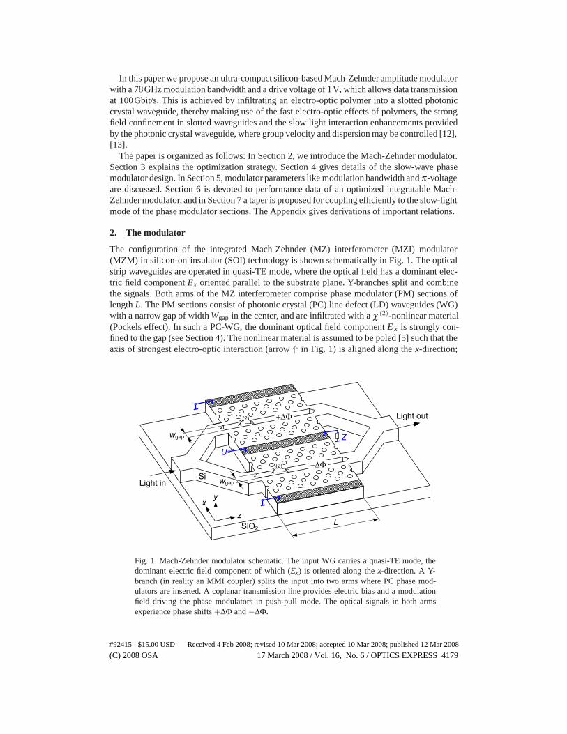
The configuration of the integrated Mach-Zehnder (MZ) interferometer (MZI) modulator(MZM) in silicon-on-insulator (SOI) technology is shown schematically in Fig. 1. The opticalstrip waveguides are operated in quasi-TE mode, where the optical field has a dominant elec-tric field component Ex oriented parallel to the substrate plane. Y-branches split and combinethe signals. Both arms of the MZ interferometer comprise phase modulator (PM) sections oflength L. The PM sections consist of photonic crystal (PC) line defect (LD) waveguides (WG)with a narrow gap of width Wgap in the center, and are infiltrated with a χ (2)-nonlinear material(Pockels effect). In such a PC-WG, the dominant optical field component E x is strongly con-fined to the gap (see Section 4). The nonlinear material is assumed to be poled [5] such that theaxis of strongest electro-optic interaction (arrow ⇑ in Fig. 1) is aligned along the x-direction;
Fig. 1. Mach-Zehnder modulator schematic. The input WG carries a quasi-TE mode, thedominant electric field component of which (Ex) is oriented along the x-direction. A Y-branch (in reality an MMI coupler) splits the input into two arms where PC phase mod-ulators are inserted. A coplanar transmission line provides electric bias and a modulationfield driving the phase modulators in push-pull mode. The optical signals in both armsexperience phase shifts +ΔΦ and −ΔΦ.
#92415 - $15.00 USD Received 4 Feb 2008; revised 10 Mar 2008; accepted 10 Mar 2008; published 12 Mar 2008
(C) 2008 OSA 17 March 2008 / Vol. 16, No. 6 / OPTICS EXPRESS 4179

the associated electro-optic coefficient is r33. Therefore, only the x-components of the opticalfield and of the modulating field are relevant. The nonlinear material is assumed to respondinstantaneously.
The silicon material of the PM sections is doped, e.g., with arsenic (n D ≈ 2× 1016 cm−3),to be sufficiently conductive (σ = 10Ω−1 cm−1) without introducing excessive optical loss.The edges of the PM silicon slabs are metalized with aluminum on top, and the three metal-lic layers (dark shading) running in parallel to the nonlinear optical WGs form a microwavecoplanar waveguide (CPWG). The two outer electrodes are grounded, and a modulating volt-age U applied to the center electrode generates a voltage wave that travels along the line anddrives the PM sections in push-pull mode. In each of the arms, the electric modulation fieldEel = U/Wgap is dominantly oriented along the x-direction and almost completely confined tothe gap. An optical quasi-TE field is launched at the input side of the MZM in Fig. 1. Thephase shifts induced on the two MZI arms by the respective PMs are +ΔΦ = +[ΔΦ 0 + ΔΦ(t)]and −ΔΦ = −[ΔΦ0 + ΔΦ(t)], where ΔΦ(t) ∼U(t) represents the time-varying part. The biasvoltage U0 is chosen such that the offset point is set to ΔΦ0 = π/4 (total phase difference2ΔΦ0 = π/2 between both arms, MZ interferometer in quadrature). For switching the MZMfrom full transmission to full extinction, the phase in each PM section must be changed fromΔΦ = −π/4 to ΔΦ = +π/4, which corresponds to a voltage change from U = −U π/4 toU = +Uπ/4. The modulation voltage U that is required to change the phase in one modulatorarm by π is called π-voltage Uπ .
If the modulator is realized as shown in Fig. 1, the Y-junctions and the transitions fromstrip-WG to slow-light slot PC-WG lead to significant reflection and light scattering, and themimimum feature sizes cannot be fabricated accurately. For a more practical design, the Y-branches should be replaced by MMI couplers. Further, an efficient transition from strip-WGto slow-light slot PC-WG is used as explained in Section 7.
3. MZM optimization strategy
An optimum MZM should provide large modulation bandwidth f 3dB, require low modulationvoltage amplitude U , should be fabricated based on CMOS processes, and it should have smallsize for easy on-chip integration. The MZM modulation bandwidth is in general limited by RC-effects and by the spatial walk-off between the electrical and optical waves. The spatial walk-offcan be avoided by a travelling-wave design, where the group velocities v g, el and vg, opt of theelectrical and optical waves are same, and where the CPWG is terminated with a matchingimpedance ZL to avoid reflections.
However, such a travelling-wave structure with a well-terminated CPWG is difficult to real-ize, especially in a wide optical and electrical frequency range. If the modulator can be madesufficiently short in length L, a match of vg, el and vg, opt is not needed. We achieve this lengthreduction by using a PC line defect WG that is designed to have low optical group velocity andthus shows an increased electro-optic interaction. The maximum modulation frequency f 3dB
is reached when the electrical modulation signal inside the electrical structure varies by morethan half a period during the propagation time t g, opt = vg, opt/L of the slow optical wave throughthe PM, see left-hand side of Eq. (1). This maximum frequency corresponds to the walk-off re-lated bandwidth derived in Section 5 under the condition v g, opt � vg, el. In addition, we find thatRC-effects do not play a significant role for our structure (see Appendix). Further, we derive inSection 5 and in the Appendix a relation for the π-voltage U π , which in a simplified form isgiven by the right-hand side of Eq. (1),
f3dB ≈ 0.5tg, opt
=0.5vg, opt
L, Uπ ∝
Wgap
r33
vg, opt
L. (1)
#92415 - $15.00 USD Received 4 Feb 2008; revised 10 Mar 2008; accepted 10 Mar 2008; published 12 Mar 2008
(C) 2008 OSA 17 March 2008 / Vol. 16, No. 6 / OPTICS EXPRESS 4180

From Eq. (1) we observe that the modulation bandwidth increases with the ratio v g, opt/L, how-ever, at the expense of an increased π-voltage, i.e., a large drive voltage amplitude. For anoptimum modulator (large bandwidth, low drive voltage) we need fixing the design bandwidthf3dB first, i. e., we have to decide for a certain ratio vg, opt/L. The modulator length L is then di-rectly related to the optical group velocity vg, opt, and a lower group velocity results in a shorterlength. To reduce the π-voltage, a PM material with large nonlinear coefficient r 33 needs to bechosen, and the gap width Wgap of the slotted waveguide should be made small. As we show inSection 4, both the optical and the microwave fields remain strongly confined to the nonlinearmaterial, even for a narrow gap width Wgap. This is a specific advantage of the slotted PC-WG.
4. Slow-wave phase modulator
Figure 2 displays the slow-wave phase modulator section in more detail. In the center of a PCline defect WG, a narrow gap Wgap is cut out in form of a slot. The PC consists of a silicon slabwith a triangular lattice of air holes having a lattice constant a. For a Wi line defect, a number ofi rows of holes are omitted. The width W1 of the resulting waveguide, see Fig. 2(b), depends oni, which need not be an integer. As explained previously, the silicon structure is covered witha highly nonlinear poled electro-optic polymer, which fills both the slot and the PC holes. Dueto the high index-contrast between silicon (nSi = 3.48) and polymer (npoly = 1.6), the opticalquasi-TE mode is mainly confined to the polymer-filled gap, Fig. 2(b) and [14].
For a minimum modulation voltage U we need to avoid any voltage drop in the siliconmaterial between the electrodes (Al in Fig. 2(a)) and the gap. To this end, the silicon must bemade sufficiently conductive by doping. Choosing then the smallest possible gap that is stillcompatible with technological constraints, and selecting a polymer with a large linear electro-optic coefficient minimizes the π-voltage Uπ , Eq. (1).
While maintaining the low group velocity of the optical mode, the PC-WG can be ad-justed such that chromatic dispersion of the optical wave is negligible, and signal distortionsare avoided. In Section 6 it is shown that such a design leads to a large MZM bandwidthf3dB = 78GHz for a drive voltage amplitude as small as U = Uπ/4 = 1V. For explaining ourPC waveguide design decisions, the following two subsections describe first a slow-wave PCslot waveguide PM and its properties, and then discuss the optimized PC slot waveguide designfor a flattened dispersion curve.
Fig. 2. Phase modulator (a) schematic and (b) dominant electric field component Ex. A slotfilled with an electro-optic polymer (EO) of width Wgap is cut in a silicon photonic crystalline-defect waveguide of width W1. The silicon slabs of height h and width w are doped forelectrical conductivity and contacted with aluminum layers. Ex is strongly confined to theslot. The phase ΔΦ of the propagating optical wave is tuned by applying a voltage to thepolymer. The triangular-lattice period is a.
#92415 - $15.00 USD Received 4 Feb 2008; revised 10 Mar 2008; accepted 10 Mar 2008; published 12 Mar 2008
(C) 2008 OSA 17 March 2008 / Vol. 16, No. 6 / OPTICS EXPRESS 4181

4.1. PC slot waveguide
PC waveguides lend themselves easily to a reduced group velocity near the edge of the Brillouinzone. A conventionally designed PC slot WG usually supports a mode with low group velocity,indeed. For a line-defect width W1 chosen to correspond to a W1.4 LD WG, the associated banddiagram is displayed in Fig. 3. The low group velocity region is marked by an oval to the right.The figure is calculated with the guided-mode expansion (GME) method [15], and simulationswith the finite integration technique (FIT) verify the results.
Fig. 3. Band diagram of W1.4 PC slot waveguide. The desired mode exhibits a low groupvelocity below the light line of the polymer cladding. PC slab height h = 220nm, polymergap width Wgap = 150nm, PC lattice period a = 408nm, hole radii r/a = 0.3, line defectwidth W1 = 1.4
√3a. The polymer refractive index is npoly = 1.6, f , k, c denote frequency,
propagation constant and vacuum speed of light, respectively.
The group velocity of the mode inside the marked region of Fig. 3 is displayed in Fig. 4(b)as a function of frequency (dashed line). The group velocity varies between nearly 0% and 6%of the vacuum speed of light c in the region below the light line. However, a high chromaticdispersion of C > 5ps/(mmnm) is also observed.
4.2. PC slot waveguide with dispersion flattening
For a better design with a lower chromatic dispersion, we optimize the hole radii r 1,2,3 and thedistances between the hole centers W1,2,3, see Fig. 4(a). As a result of the optimization processwe find a set of W1.25 WGs that all provide a low group velocity over a wide spectral range.The frequency dependence of the resulting group velocity with various radii r 2 as parametersis shown in Fig. 4(b). An increase of the parameter r2 decreases the group velocity, while a flatdispersion is maintained. For the value r2/a = 0.36, the group velocity is 4% of the vacuumspeed of light c over a bandwidth of about 1THz. It is also possible to obtain a negative chro-matic dispersion, which is for example the case for r2/a = 0.30 or r2/a = 0.38, Fig. 4(b). Forall presented designs, the air hole diameters are larger than 200nm in order to meet fabricationconstraints. The concept of the PC-WG with broadband low group velocity was experimentallyverified previously [13].
#92415 - $15.00 USD Received 4 Feb 2008; revised 10 Mar 2008; accepted 10 Mar 2008; published 12 Mar 2008
(C) 2008 OSA 17 March 2008 / Vol. 16, No. 6 / OPTICS EXPRESS 4182

192 194 196 198 2000.00
0.05
0.10
0.15
0.38
0.360.34
0.32
r2 / a = 0.30
vg
c
Frequency f (THz)
Fig. 4. W1.25 PC slot waveguide with slab height h = 220nm, polymer gap width Wgap =150nm, PC lattice period a = 408nm. (a) Structure parameters and (b) group velocity asa function of frequency with varying hole radii r2. With r2/a = 0.36, the group veloc-ity amounts to 4% of the vacuum speed of light c, and the group velocity dispersion isnegligible in a bandwidth of 1THz. For comparison, the group velocity of the conven-tional W1.4-WG of Fig. 2 is plotted as a dashed line (W1 = 1.4
√3a, W2 = W3 = 0.5
√3a,
r1 = r2 = r3 = r = 0.3a). Parameters of the W1.25-WG are W1 = 1.25√
3a, W2 = 0.65√
3a,W3 = 0.45
√3a, r1 = 0.25a, r3 = r = 0.3a.
5. Modulator performance parameters
The main performance parameters for the modulator are the MZM modulation bandwidth f 3dB
and the phase modulator π-voltage Uπ . The two parameters are derived and discussed in thissection.
5.1. Modulation bandwidth of Mach-Zehnder modulator
The bandwidth of the MZM is limited by the walk-off between electrical and optical waves. RClimitations do not play a role for the presented structures as has been shown in the Appendix.The walk-off limited bandwidth depends on the termination of the CPWG, and here we discussthe two cases of a matched load and an open.
1) Walk-off bandwidth, CPWG with matched load
The CPWG be ideally terminated with a matched load so that the modulating wave travelingalong z is not reflected at the end of the CPWG and maintains a spatially constant amplitude|U |. Electrical and optical waves propagate in the same direction, but in general at differentgroup velocities vg, el and vg, opt (group delays tg, el and tg, opt over the PM section length L).The nonlinear interaction is maximum for co-directionally traveling waves (TW) with t g, el =tg, opt, and it decreases strongly if tg, el �= tg, opt. When the electrical and optical signal envelopeshave acquired a phase difference of π , the limiting modulating frequency f 3dB is reached with
#92415 - $15.00 USD Received 4 Feb 2008; revised 10 Mar 2008; accepted 10 Mar 2008; published 12 Mar 2008
(C) 2008 OSA 17 March 2008 / Vol. 16, No. 6 / OPTICS EXPRESS 4183

ω (TW)3dB |tg, opt − tg, el| = π , i. e.,
f (TW)3dB =
0.5|tg, opt − tg, el| =
0.5vg, opt
L1
|1− vg, opt/vg, el| . (2)
Following the formalism in [16], a more accurate formula can be derived, whereby it is shownthat the factor of 0.5 in Eq. (2) need be replaced by 0.556.
2) Walk-off bandwidth, CPWG with open-circuit
In order to keep the design of an integratable MZM simple, the CPWG would be morefavourably be configured without terminating resistances. Because of the reflection at the openCPWG, a standing wave results. For the forward propagating part of the electrical wave, Eq. (2)specifies the limiting frequency. However, the backward propagating wave puts a tighter walk-off limit, because now the electrical wave has the opposite direction compared to the opticalwave. With similar arguments that led to Eq. (2) we find ω3dB|tg, opt + tg, el| = π ,
f3dB =0.5
|tg, opt + tg, el| =0.5vg, opt
L1
|1+ vg, opt/vg, el| . (3)
As above, a more accurate formula can be developed following [16] where the factor of 0.5 inEq. (3) is again replaced by 0.556. If vg, opt � vg, el holds, then f3dB ≈ f (TW)
3dB and electricallyshort MZM designs with and without matching load for the CWPG become nearly equivalent,resulting in Eq. (1).
5.2. π-voltage Uπ of phase modulator
A Mach-Zehnder modulator’s sensitivity is characterized by the π-Voltage U π of its phase mod-ulators. For a given PM length L the voltage |U | needed for a π-phase shift is defined to be U π .For large modulation sensitivity, Uπ should be small. An optical wave propagating through aPM experiences a nonlinear refractive index change Δn in proportion to the electric modulatingfield Eel inside the nonlinear PM material,
Δn = −12
r33 n3poly Eel, Eel = U/Wgap . (4)
As before, npoly represents the effective linear part of the refractive index in the PM section,and r33 is the (scalar) linear electro-optic coefficient. The total phase shift of the optical wavedue to the index change in a PM section of length L is (following the formalism in AppendixSection A and in [16])
ΔΦ = −Δβ L = −ΓΔnk0L . (5)
The quantity k0 = 2π f0/c is the vacuum wave number. In the process of deriving Eq. (5) theso-called field interaction factor Γ was introduced. It quantifies the strength of the nonlinearelectro-optic interaction of modulating field and optical mode in a cross-section A along alattice period a (see Appendix Eqs. (8)-(13) and [16]),
Γ =∫
gap
nZ0
|Ex|2 dV
/∫aℜ(E× H∗) · ez dA ∝
1vg, opt
. (6)
In Eq. (6), Z0 is the free-space wave impedance, E (x-component Ex) and H are the opticalmodal electric and magnetic fields, and ez is the unit vector in z-direction. The field interactionfactor Γ as defined in Eq. (6) is different from the field confinement factor, which is usuallycalculated as a ratio between the optical power in the cross-section of the interaction region
#92415 - $15.00 USD Received 4 Feb 2008; revised 10 Mar 2008; accepted 10 Mar 2008; published 12 Mar 2008
(C) 2008 OSA 17 March 2008 / Vol. 16, No. 6 / OPTICS EXPRESS 4184

and the total power propagating in the whole modal cross-section. While the field confinementfactor varies between 0 and 1, the field interaction factor Γ can be larger than 1. The integralin the numerator of Eq. (6) is a measure of the energy stored in the transverse componentof the propagating optical mode inside the PM along a length a (see Appendix, Eq. (16)).The denominator represents the transported power in the modal cross-section. According toEq. (17), the energy stored in a volume, when related to the cross-section power of a wavethat crosses this volume, increases in proportion to the reciprocal group velocity of the wave.Because in the numerator of Γ only the dominant transverse field component is regarded, theproportionality Γ ∝ 1/vg, opt holds only approximately. Application of a voltage Uπ to the PMresults by definition in a phase change of ΔΦ = π within a length L. From Eq. (4)-(6), theπ-voltage is computed to be
Uπ =c
n3poly f0
Wgap
r33
1LΓ
, Uπ ∝Wgap
r33
1LΓ
∝Wgap
r33
vg, opt
L∝
Wgap
r33f3dB . (7)
For the proportionality at the right-hand side of Eq. (7), the relations Γ ∝ 1/v g, opt and f3dB ∝vg, opt/L were substituted from Eq. (6) and Eq. (3).
6. Optimized Mach-Zehnder modulator
For maximizing the modulation bandwidth f 3dB, Eq. (3), of the MZM amplitude modulator andfor minimizing its π-voltage Uπ , Eq. (7), the optical group velocity vg, opt of the PC line defectWG, its length L, the electro-optic coefficient r33 of the polymer, and the gap width Wgap needto be adjusted properly. For an integratable MZM with small length L, the design bandwidthf3dB fixes the ratio vg, opt/L. Reducing vg, opt then provides a small length L. It also needs to beconsidered that with lower vg, opt, the disorder-induced losses of the PC-WG increase [17] andthe optical bandwidth decreases, so that vg, opt cannot be made arbitrarily small.
For a small Uπ , the electro-optic polymer is chosen to have a large linear electro-optic coeffi-cient of r33 = 80pm/V [6]. Further, Wgap is chosen as small as compatible with the fabricationprocess. A gap width of Wgap = 150nm can be fabricated to good accuracy with advanced litho-
Structure r2 / a fo (THz) vg,opt/c L ( m) f3dB (GHz)
0.3 196.4 2.4% 4.8 36 103 196.6 3.4% 3.2 54 97 196.9 4.8% 2.2 80 90 196.2 6.4% 1.5 113 83
W1.4dispersion
large
197.7 8.2% 1.1 155 76
0.38 197.5 3.2% 3.1 57 87 0.36 196.5 4.0% 2.2 80 78 0.34 195.8 5.2% 1.6 111 71 0.32 195.2 6.6% 1.1 158 61
W1.25dispersion flattened
0.30 194.6 7.9% 0.8 215 53
Table 1. Characteristic data for a PC slot waveguide modulator. Group velocity vg,opt,field interaction factor Γ, modulator length L and modulation bandwidth f3dB are esti-mated at different optical carrier frequencies f0. We assume an electro-optic coefficientof r33 = 80pm/V. The modulation voltage amplitude for maximum extinction is fixed toU = Uπ/4 = 1V.
#92415 - $15.00 USD Received 4 Feb 2008; revised 10 Mar 2008; accepted 10 Mar 2008; published 12 Mar 2008
(C) 2008 OSA 17 March 2008 / Vol. 16, No. 6 / OPTICS EXPRESS 4185

graphic processes; hence this width is fixed for the present design. Given the gap width W gap,the maximum modulation voltage amplitude is limited in practice by the microwave source andby dielectric breakdown in the gap.
In Table 1, we list group velocity vg, opt, field interaction factor Γ, modulator length L, andmodulation bandwidth f3dB for various PC slot waveguide modulators without (W1.4) and withdispersion flattening (W1.25), as already presented in Section 4. The π-voltage was kept fixedto Uπ = 4V in all cases, which means that the modulation voltage amplitude U = Uπ/4 = 1Vremained constant by adjusting the length L according to Eq. (7).
The values vg, opt and Γ are calculated from simulations with the FIT method. As expected,the field interaction factor Γ increases and the modulator length L decreases when lowering thegroup velocity vg, opt according to Eqs. (6), (7). The bandwidth f 3dB is calculated from Eq. (3)using the more exact numerical factor of 0.556 instead of 0.5. For a constant U π the estimateEq. (1) would predict a constant modulation bandwidth f 3dB, however, it shows a weak (1 : 1.4)dependence on vg, opt (1 : 3.4). This is explained after Eq. (6): The field interaction factor Γ isonly approximately proportional to 1/v g, opt, and therefore Uπ ∝ vg, opt in Eqs. (7), (1) is anapproximation, too. For the dispersion flattened structures, f 3dB is lower and shows a strongerdependence on vg, opt compared to the structure with high dispersion.
The disorder-induced losses of a slow-light PC-WG operated at a group velocity of 5.8% ofthe vacuum speed of light were measured to be 4.2dB/mm [18]. Doping silicon with a largeconcentration of phosphorus atoms (2× 10 18 cm−3) leads to additional optical losses of onlyabout 1dB/mm [7]. At a slightly smaller group velocity of 4% of the vacuum speed of lightand a moderate doping concentration of 2×10 16 cm−3, optical losses will be mainly caused bydisorder. With small device lengths the additional loss is expected to be tolerable.
Because the dispersion-flattened structure shows a large modulation bandwidth of f 3dB =78GHz at a length of only L = 80 μm and for a small 1V drive voltage amplitude, we regardthis to be an optimum structure for the discussed technological constraints.
7. Slow-light coupling structure
Signals from an external fiber may be effectively coupled to a conventional strip WG modewith coupling losses below 1dB [19]. However, an efficient method is also needed to excitethe slow-light mode within the PC slot WG. We propose a coupling structure consisting of twosections, which are schematically shown in Fig. 5.
Fig. 5. Schematic of the coupling structure. (a) Transition from strip-WG to slot-WG (b)Coupling to PC WG. The transmission is significantly increased by introducing a PC taper,where the width W1 of the PC-WG is slightly decreased from 1.45
√3a to 1.25
√3a over
some lattice periods, indicated by the overlaid tilted (green) lines, and the width W2 isincreased from 0.55
√3a to 0.65
√3a. The width of the strip-WG is 440nm, and the gap
width of both the slot-WG and the PC-WG is 150nm.
#92415 - $15.00 USD Received 4 Feb 2008; revised 10 Mar 2008; accepted 10 Mar 2008; published 12 Mar 2008
(C) 2008 OSA 17 March 2008 / Vol. 16, No. 6 / OPTICS EXPRESS 4186

The first section transforms1 the strip WG mode into a slot-WG mode, Fig. 5(a). The designtakes into account that the silicon on both sides of the gap needs to be electrically isolated asit is conductive and carries the modulation voltage, Fig. 2(a). FIT simulations of the strip-to-slot WG transition having a length of 7 μm predict a transmission loss lower than 0.3dB and areflection lower than −28dB.
The second section couples the slot WG to the slow-light PC WG, Fig. 5(b). We developed ataper where the width of the PC WG is slightly decreased over a length of 10 periods (4.08 μm)to gradually slow down the PC WG mode. The calculated transmission and reflection curvesare displayed in Fig. 6. The simulated structure comprises both the transition from a slot WGto a slow-light PC WG, Fig. 5(b), and the transition back to a slot WG.
Fig. 6. Transmission and reflection for the transition from slot-WG to PC-WG and backto slot-WG, Fig. 5(b), with and without a PC taper. The introduction of the PC taper sig-nificantly enhances the transmission to a value better than −4dB. The reflection is below−10dB.
The transmission is better than −4dB including both tapers, while it drops below −20dBwithout tapers. The reflection stays below −10dB. In the transmission curve with tapers, rip-ples can be observed. These are Fabry-Perot fringes generated by residual reflections at theinterfaces. These reflections can be decreased by optimizing the transitions, and an extensionof the taper sections lengths can further improve the device characteristics.
8. Conclusion
We propose a high-speed silicon modulator with low drive voltage based on a polymer-infiltrated slow-light photonic crystal line-defect waveguide. For a design with negligible first-order chromatic dispersion in an optical bandwidth of 1THz we predict a modulation band-width of 78GHz and a length of about 80 μm at a drive voltage amplitude of 1V. This allowstransmission at 100Gbit/s.
1We thank an anonymous referee for pointing out a patent application, which describes such a structure: M. Lipson,C. A. Barrios, V. R. Almeida, R. R. Panepucci, and Q. Xu, United States Patent Application 20060228074.
#92415 - $15.00 USD Received 4 Feb 2008; revised 10 Mar 2008; accepted 10 Mar 2008; published 12 Mar 2008
(C) 2008 OSA 17 March 2008 / Vol. 16, No. 6 / OPTICS EXPRESS 4187

Appendix
A. Field interaction factor Γ
For the derivation of the field interaction factor Γ we follow the formalism in [16]. The influ-ence of the microwave field on the optical mode through the electro-optic effect is treated as aperturbation Δε on the permittivity of the material in Maxwell’s equations
∇×E = −μ∂H/∂ t , (8)
∇×H = ∂ [(ε + Δε)E]/∂ t . (9)
For a mode propagating inside a PC WG along the z-direction, a complex envelope function Ais defined,
E(x,y,z,t) = A(z,t)E(x,y,z)ej(ω0t−β0z), (10)
H(x,y,z,t) = A(z,t)H(x,y,z)e j(ω0t−β0z) . (11)
The field distribution of the mode is taken at the optical carrier frequency f 0 = ω0/(2π) andis assumed to be constant in the optical signal bandwidth centered at f 0. For the propagationconstant β of the mode we assume β (ω)= β0+(ω−ω0)v−1
g, opt neglecting chromatic dispersion.
The orthogonality relation for two WG modes Hp, q, Ep, q subscripted with p and q, respectively,and having the same frequency can be derived following [20],
∫(Eq × H∗
p − Hq × E∗p) · ez dA = 4δpqPp . (12)
Here, δpq is the Kronecker delta, Pp is the cross-section power of mode p, and the integration isperformed over a cross-section perpendicular to the propagation direction. If Eqs. (10), (11) aresubstituted in Eqs. (8), (9), and both the mode orthogonality condition Eq. (12) and the slowlyvarying envelope approximation are used, a nonlinear propagation equation is obtained,
∂A∂ z
+1
vg, opt
∂A∂ t
= jω0ΓKUA, A = |A|ej(Φ+ΔΦ) . (13)
In Eq. (13), the relations A = A(z,t), U =U(z,t), Φ = Φ(z,t) and ΔΦ = ΔΦ(z,t) hold. The fieldinteraction factor Γ is defined in Eq. (6), K = ε0
2 r33n3polyZ0/Wgap is a constant, and U = U(z,t)
is the voltage across the gap. It is generated by the microwave field that causes an electro-opticrefractive index change Δn = −r33n3
polyU/Wgap and a resulting phase change ΔΦ.
B. Relation between field interaction factor Γ and group velocity v g,opt
We first sketch the derivation of the dependence of the power flow on group velocity. Observingthat the nonlinear perturbation of the permittivity is small, Δε � ε , we substitute the modalfields Eqs. (10), (11) with A = 1 into Eq. (11) and obtain
∇× H− jβ0ez × H = jω0εE . (14)
From this equation, we write the total differential with respect to the variables β 0 and ω0 andfind
−dβ0(ez × H) = dω0εE . (15)
We form the scalar product of the complex conjugate of Eq. (15) with E and the scalar productof Eq. (15) with E∗. Then we add both relations, observe (e z× H∗) · E = (H∗× E) ·ez = −(E×H∗) · ez, and integrate over a volume V = aA with differential dV = a dA, where dA is the
#92415 - $15.00 USD Received 4 Feb 2008; revised 10 Mar 2008; accepted 10 Mar 2008; published 12 Mar 2008
(C) 2008 OSA 17 March 2008 / Vol. 16, No. 6 / OPTICS EXPRESS 4188

differential of the cross-section area A in a plane z = const. For PC WGs, the length a along thewaveguide’s z-axis corresponds to the size of the unit cell. We find
dβ0
∫14 (E× H∗+ E∗ × H) · ez dV = dω0
∫12 ε|E|2 dV . (16)
The right-hand side integral of Eq. (16) is the mean stored energy at frequency f 0 inside thevolume under consideration. The integrand on the left-hand side of Eq. (16) is the real part ofthe z-component of the complex Poynting vector 1
2 E× H∗. Its integral over the cross sectionarea A is independent of the z-position. So the volume integral may be written as an integralover the cross-section multiplied by the length a of the volume along z. The result is
1vg, opt
=dβ0
dω0=
∫ 12 ε|E|2 dV
a∫
ℜ( 12 E× H∗) · ez dA
. (17)
Equation (17) can be understood intuitively: The energy stored in a volume V = aA per transittime a/vg, opt of the wave that crosses this volume equals the cross-section power. Thus for afixed amount of transmitted power, the stored energy increases inversely proportional to thegroup velocity. Relation (17) resembles but is distinct from the field confinement factor Eq. (6),where the power in the waveguide core is related to the total cross-section power: The morepower is concentrated to the core, the larger the propagation constant becomes, and the slowerthe wave propagates.
C. Modulator bandwidth limitations by RC-effects
We estimate the modulator bandwidth limitations that are caused by electrical RC-effects. Wediscuss two different mechanisms that reduce the electrical voltage drop across the gap andlead to an associated 3dB bandwidth. These are the generator-determined bandwidth and theparallel-loss determined bandwidth. We find that these bandwidth limitations do not play asignificant role for the presented structures.
For the following numerical examples, the data of our specific MZM design for a 78GHzmodulation bandwidth and a drive voltage of 1V were assumed, Fig. 1 and Fig. 2: Optical stripwaveguide height h = 220nm, PM section length and gap width L = 80 μm and W gap = 150nm,linear refractive index of the PM section npoly = 1.6 (assumed to be the same at optical andelectrical frequencies), width of the doped silicon slabs w = 3 μm, vacuum dielectric constantε0, vacuum speed of light c.
1) Generator-determined bandwidth
The CPWG with wave impedance ZL = 50Ω be terminated with an open, Fig. 7(a). We assumethe PM section to be short compared to the modulation signal wavelength, so that the CPWGmay be represented by a lumped gap capacitance Cgap = ε0n2
polyhL/Wgap for each PM. Thevoltage amplitude Ugap across the non-conductive gap Wgap (i. e., across the lumped capacitor2Cgap) decreases with modulation frequency f because of the generator impedance R G = 50Ω,
Ugap
UG=
11+ jωRG2Cgap
, f(RGCgap)3dB =
14πRGCgap
. (18)
At the limiting frequency f(RGCgap)3dB the gap voltage |Ugap| drops to |UG|/
√2. Assuming the pre-
viously assigned data and neglecting electric fringing fields, the total gap capacitance amounts
to 2Cgap = 5fF, and f(RGCgap)3dB ≈ 640GHz results. In view of the envisaged MZM bandwidth of
78GHz, the generator-determined limitation is unimportant.
#92415 - $15.00 USD Received 4 Feb 2008; revised 10 Mar 2008; accepted 10 Mar 2008; published 12 Mar 2008
(C) 2008 OSA 17 March 2008 / Vol. 16, No. 6 / OPTICS EXPRESS 4189

Fig. 7. Electrical RC-effects. (a) Generator-determined limitation (b) Parallel-loss deter-mined limitation. In (a), the electrically short PM section is represented by a lumped gapcapacitance Cgap, and the voltage across the gap Ugap is only a fraction of the generatorvoltage UG because of the generator impedance RG. In (b), a voltage wave with constantamplitude |U | travels in z-direction. The voltage Ugap across the gap (capacitance per lengthC′) is reduced because of the finite resistivity of the doped silicon sections of width w (con-ductance per length (R′−1).
2) Parallel-loss determined bandwidth
The CPWG be terminated with its wave impedance ZL, Fig. 7(b). Then, a modulating electricalwave traveling in z-direction has a spatially constant amplitude |U |. The resulting voltage ampli-tude |Ugap| across the non-conductive gap Wgap (PM capacitance per length C ′ = ε0n2
polyh/Wgap)is reduced because of the finite resistivity of the doped silicon. For silicon sections having awidth w and a filling factor F taking the reduction of the effective conductance by the air holesinto account (conductance per length (R ′−1 = σFh/w), we obtain
Ugap
U=
11+ jω2R ′C′ , f (R ′C′)
3dB =1
4πR ′C′ (19)
The limiting frequency f (R ′C′)3dB denotes where the gap voltage |Ugap| drops to |U |/√2. Assuming
a conductivity σ = 10Ω−1 cm−1 of the doped (nD ≈ 2×1016 cm−3) silicon material and a filling
factor F = 0.67, a bandwidth of f (R ′C′)3dB ≈ 120GHz results. In view of the envisaged MZM
bandwidth of 78GHz, the parallel-loss determined limitation does not play a significant roleeither.
3) Other effects
Basically, one might think of a bandwidth limitation by the finite carrier transit time in the dopedsilicon slabs, see Fig. 2. This carrier drift time is determined by the slower carriers, which insilicon are holes, the maximum saturation velocity of which is about 0.6×10 7 cm/s. Over the3 μm witdh of the silicon slab, this would lead to a response time in the order of τ D = 50ps,resulting in a bandwidth in the order of 3GHz only.
However, there is also the dielectric dielectric relaxation time τR, inside which any chargeperturbation in the doped silicon slabs (induced by the modulating field) is screened by a shiftof the whole carrier ensemble. The dielectric relaxation time τ R = ε0 εr/σ depends on the ma-terial’s conductivity σ and permittivity ε0 εr. For σ = 10Ω−1 cm−1 as assumed above and withεr = 12, a value of τR = 0.1ps is obtained.
For the resulting response time τ−1res = τ−1
D + τ−1R ≈ τ−1
R , the faster of the two effects isrelevant, and the bandwidth limited by the dielectric relaxation time would be 1.6THz. As aconsequence, carrier transit times do not limit the modulator’s performance.
#92415 - $15.00 USD Received 4 Feb 2008; revised 10 Mar 2008; accepted 10 Mar 2008; published 12 Mar 2008
(C) 2008 OSA 17 March 2008 / Vol. 16, No. 6 / OPTICS EXPRESS 4190

Acknowledgment
This work has been supported by the Deutsche Telekom Stiftung, by the Deutsche Forschungs-gemeinschaft (DFG) in the framework of the Priority Program SP 1113 “Photonic Crystals“and by the Center of Functional Nanostructures (CFN) within projects A3.1 and A4.4.
#92415 - $15.00 USD Received 4 Feb 2008; revised 10 Mar 2008; accepted 10 Mar 2008; published 12 Mar 2008
(C) 2008 OSA 17 March 2008 / Vol. 16, No. 6 / OPTICS EXPRESS 4191