electro-optic spatial light modulator from an engineered
TRANSCRIPT
ARTICLE
Electro-optic spatial light modulator from anengineered organic layerIleana-Cristina Benea-Chelmus 1✉, Maryna L. Meretska 1, Delwin L. Elder 2, Michele Tamagnone 1,
Larry R. Dalton 2 & Federico Capasso 1✉
Tailored nanostructures provide at-will control over the properties of light, with applications in
imaging and spectroscopy. Active photonics can further open new avenues in remote monitoring,
virtual or augmented reality and time-resolved sensing. Nanomaterials with χ(2) nonlinearities
achieve highest switching speeds. Current demonstrations typically require a trade-off: they either
rely on traditional χ(2) materials, which have low non-linearities, or on application-specific quantum
well heterostructures that exhibit a high χ(2) in a narrow band. Here, we show that a thin film of
organic electro-optic molecules JRD1 in polymethylmethacrylate combines desired merits for
active free-space optics: broadband record-high nonlinearity (10-100 times higher than traditional
materials at wavelengths 1100-1600 nm), a custom-tailored nonlinear tensor at the nanoscale, and
engineered optical and electronic responses. We demonstrate a tuning of optical resonances by
Δλ= 11 nm at DC voltages and a modulation of the transmitted intensity up to 40%, at speeds up
to 50 MHz. We realize 2 × 2 single- and 1 × 5 multi-color spatial light modulators. We demon-
strate their potential for imaging and remote sensing. The compatibility with compact laser diodes,
the achieved millimeter size and the low power consumption are further key features for laser
ranging or reconfigurable optics.
https://doi.org/10.1038/s41467-021-26035-y OPEN
1 Harvard John A. Paulson School of Engineering and Applied Sciences, Harvard University, Cambridge, MA, USA. 2Department of Chemistry, University ofWashington, Seattle, WA, USA. ✉email: [email protected]; [email protected]
NATURE COMMUNICATIONS | (2021) 12:5928 | https://doi.org/10.1038/s41467-021-26035-y | www.nature.com/naturecommunications 1
1234
5678
90():,;
Recent advances in both traditional and novel electro-opticmaterials that exhibit a χ(2) nonlinearity have resulted intoan unprecedented richness of active photonic devices, that
find applications in communications1–3, electric field metrology4,5,dynamic beam steering6, and quantum science7. Multi-pixel, large-area spatial light modulators (SLMs) are a prerequisite to achievemassively parallel dynamic and reconfigurable control over thediverse properties of light. They promise to revolutionize appli-cations in industry and fundamental science. In reconfigurablephotonics, multipixel optical components can control light on-demand, but they need to be compact and consume minimalpower per pixel. In massively parallel remote sensing8, high-speedSLMs can generate parallel optical channels that scan the envir-onment in three dimensions, but operation at high speeds ismandatory to resolve small changes in the position and velocity ofobjects within a short timeframe. In the area of ultrafast optics,SLMs can manipulate femtosecond pulses through pulse-pickers,but must accommodate a broad optical bandwidth and switchingspeeds commensurate with the repetition rate of these lasers,typically around few MHz to GHz. In fundamental science, SLMsplay a crucial role e.g., in the sorting and reconfiguration of coldatoms for quantum simulation9, and reaching higher speeds canaccess entirely new physics. In industry applications, such as self-driving cars10, high-speed SLMs can monitor a scene if they arecompatible with low-power electronic circuits, chip-based laserdiodes that typically have a broad linewidth and low foot-printpackaging.
Among all existing SLM technologies, SLMs that employ electrictuning enabled by χ(2) materials are outstanding candidates toreach high speeds in parallel multipixel architectures. They areintrinsically compatible with massively parallel radio-frequency(RF) electronic circuits that promise to deliver the necessaryelectrical controls by hybrid electronic-optical integration. In thiscase, the SLM is essentially a two-dimensional array of free-spaceelectro-optic modulators. Commercial SLMs instead use bulkydigital micro-mirror arrays11 or liquid crystals12, which not onlylimit them to around 10 kHz but also do not employ nanos-tructures. Few state-of-the art SLM demonstrations address thequest for ever-higher speed by making use of narrow-band surfaceplasmon resonances in rather complex prism-based schemes usingχ(2) nonlinear materials13, but the nano-scale engineering of theindividual pixels remains unexplored and the employed non-linearity is rather low. Flat lens technology around metasurfaces14
is a powerful platform that permits engineering of the properties oflight at a sub-wavelength scale in an extremely compact device.Static single-pixel metasurfaces have addressed multiple needs(focussing, polarization control15, or correcting optics16) or mul-tipixel metasurfaces (next-generation biodevices17). Consequently,an ideal platform for high-speed SLMs combines high-performance χ(2) materials with nanostructures. Current demon-strations of monolithic metasurfaces from χ(2) materials typicallytrade off an operation around a sharp resonance in materials withmoderate but broadband χ(2) effect e.g., in lithium niobate18,19 orcolloidal nonlinear nanocubes20 against an efficient χ(2) effect inapplication-specific engineered III–V heterostructures, which ishowever narrowband and located around its bandgap6. Whilemany demonstrations are single-pixel, few exciting multifunctionalmetasurfaces with multiple electronic controls have emergedexperimentally6,21,22 and theoretically23. Important to mention arealso metasurfaces based on transparent conductive oxides22,24–26
that have enabled SLMs recently27, gate-tunable low-dimensionalmaterials28 or phase change materials such as e.g., GST29–33 thatare excellent candidates in scenarios, where high switching speedsare not required. Microelectromechanical34,35 or thermo-opticallycontrolled36 systems are ideal for low speed applications that donot require pixel-level control.
Custom-engineered organic nonlinear molecules insteadovercome this bandwidth-nonlinearity limitation since they haveelectro-optic coefficients that are 10–100 times higher thanstandard materials (up to r33 = 560 pmV−1 in bulk layers and200 pmV−1 in nanoplasmonic gaps of gold electrodes37), over theentire band from 1100 to 1600 nm (see Supplementary Note 7).They are anticipated to deliver high-end SLMs, owing to theirterahertz-compatible bandwidth (up to 2.5 THz38), high index ofrefraction and recently reported long-term thermal and chemicalstability39. Only little work studies such molecules beyond siliconphotonic circuits (where they reach highest electro-opticcouplings4 and integration with complementary metal-oxide-semiconductor (CMOS) electronics40) for large-area electro-opticmodulators, even in the single pixel case41,42. The only SLMsdemonstrated so far to the best of our knowledge employ verticalFabry-Perot geometries that do not exploit nano-engineering, andforce an operation with the much lower r13 electro-opticcoefficient43.
In this work, we experimentally demonstrate that a single layerof organic non-linear material (here JRD1 mixed with PMMA)enables custom-tailored engineering of each pixel of an SLMwhile, at the same time, providing a high modulation efficiencythrough r33, compatibility with broadband lasers, linearity todriving voltage, low power consumption, and high speed. Thisstems from our ability to manipulate the tensorial properties ofthe nonlinearity (magnitude and orientation) of the thin film atthe nanoscale at will by electric field poling44, and influence theelectric current per pixel by mixing of JRD1 with PMMA.
ResultsElectro-optic spatial light modulator concept. The proposeddevice is depicted in Fig. 1 and is utilized to realize single-color ormulticolor SLMs at high rates and achieve remote sensing byencoding space information onto the radio-frequency domain.An array of free-space electro-optic modulators controls thetransmission of an incident beam in the transverse plane. Eachelectro-optic modulator exhibits a resonance, around which thetransmission changes dramatically. Being covered by a singlelayer of organic electro-optic molecules, the resonant wavelengthof each modulator shifts under an applied driving voltage via ther33 component of the Pockels effect (see inset for behavior aroundthe operation wavelength λop as a function of voltage). A singleelectro-optic modulator is explained in Fig. 2a and fabricateddevices are shown in Supplementary Fig. 12: metallic stripes oftotal thickness hAu from titanium and gold (of thickness 15 nmand 25/35 nm, respectively and width 200 nm, see scanningelectron micrograph in Supplementary Fig. 12c) are assembledinto a linear array and covered by a film of organic electro-opticmolecules JRD1 mixed with PMMA with 50 wt% (represented ingreen in Fig. 2a and shown in the photo in SupplementaryFig. 12b and the bright field image in Supplementary Fig. 12d).The film is cast post-fabrication, at which point it is not active yet.The interdigitated metallic array serves three distinct purposes: 1.it is used to render the organic thin film electro-optically active bya poling procedure during which the orientation of the organicmolecules (and thereby their electro-optic coefficient r33) isoriented, at the nanoscale, along an applied DC electric field,owing to their hyperpolarizability, 2. it sustains the generation ofguided mode resonances45 that introduce a voltage-dependenttransmission of the incident beam, and 3. it is used post-activation as contacts for the RF drives of the modulators.
The organic film is poled in-plane44, shown in the upper insetof Fig. 2a. Adjacent unit cells of the array are poled in anti-parallel directions, yielding an in-plane periodically poled (PP)JRD1:PMMA film (in-plane PP-JRD1:PMMA) with alternating
ARTICLE NATURE COMMUNICATIONS | https://doi.org/10.1038/s41467-021-26035-y
2 NATURE COMMUNICATIONS | (2021) 12:5928 | https://doi.org/10.1038/s41467-021-26035-y | www.nature.com/naturecommunications
electro-optic coefficients r33 (blue) and −r33 (red). Consequently,all unit cells exhibit the same refractive index change ΔnðtÞ ¼� 1
2 n3matr33EACðtÞ (see lower inset of Fig. 2a, marked green), which
depends linearly on the tuning voltage VAC applied to thecontacts EACðtÞ ¼ VACðtÞ
wgap. nmat is the material refractive index at
the wavelength of the resonant mode (see Fig. 2b). A change intopography is observed after poling, see dark field and atomicforce microscopy in Supplementary Fig. 12e, f. The characteristiccurrent–voltage (I–V) curve of the modulator is shown Fig. 2d upto bias fields similar to poling fields, around of 100 V μm−1. Thedevice exhibits the characteristics of a metal-semiconductor-metaljunction. Consequently, the tunneling current of one pixel istypically below 100 nA, even for a total modulator area oflel × lel= 390 μm× 390 μm. Details on the electronic structure ofJRD1 can be found for example in Ref. 46. The available tuningrange spans from −Epol to +Epol. For our study, we purposefullychose large pixel arrays, as opposed to small pixels, in order todemonstrate both the low electric power consumption below 10μW (corresponding to electrical switching energies below 10 pJ at1 μs), and the ability to activate at once and drive in parallelmillimeter-sized SLMs using a single JRD1:PMMA layer.
Resonance engineering. The optical guided mode resonances(see Fig. 2c) arise through the interplay between the metallic arrayand the layer of JRD1:PMMA45 with dielectric properties asshown in Fig. 2b. The full refractive index data is provided forvarious concentrations of the JRD1:PMMA compound in theSupplementary Note 6 and in the data associated with thismanuscript. In short, an incident beam is diffracted by the arrayinto grating orders, which correspond, at given angles, to guidedmodes in the slab formed by JRD1:PMMA of hJRD1= 690 nm and
surrounded by air above and quartz below. Owing to reciprocity,the grating also scatters the guided light back which interfereswith the incident light to create well-defined resonances. In bothexperiment and simulation, we vary the periodicity of the arraywfield between 0.8 and 1.4 μm and target three different guidedmode resonances of different in-plane wavevectors kz (I., II., andIII.) in Fig. 2f which have typical field distributions with corre-sponding real part of their x-component and z-component asshown in Fig. 2g. Their linewidth increases with increasingthickness of the metal (see Supplementary Note. 4A). Theiroptical field overlaps well with the simulated DC field distributionbetween the two electrodes as plotted in Fig. 2e, which governsthe orientation of the r33 component. We note that as a result ofthe spatially varying magnitude and orientation of the polingfield, the electro-optic coefficient r33 and the refractive indexchange Δn also vary spatially. A detailed discussion is provided inthe Supplementary Note 3. We probe the optical properties of themodulators by shining a focused beam of light from a super-continuum laser (SuperK Select) polarized in the z-direction. Werecord the transmission as a function of wavelength and find thatour simulations reproduce well the wavelength dependence of theresonances, reported in Fig. 2f. We find that for wavelengths closeto 1100 nm, the high loss of the JRD1:PMMA (see ϵi in Fig. 2b)broadens the resonances and limits their depth. We note that thebroad bandwidth of the probe light (5–10 nm, shown in Sup-plementary Note 4D), combined with its focussing onto thesample using a lens of focal length f= 60 mm, obscure the reallinewidth in measurements. The resonant wavelength shifts lin-early with driving voltage:
ΔλresðtÞλres
¼ �ΔωresðtÞωres
¼ ΔnðtÞnmat
Γc ¼Δneff ðtÞnmat
; ð1Þ
Fig. 1 Large area, high-speed, electro-optic spatial light modulator for massively parallel imaging or remote sensing. A beam of light Einc is incident ontoan array of n × n electro-optic modulators that are controlled by a set of driving voltages Vn at radio-frequencies fmod;n. The modulators are resonant bydesign and covered by a single layer of electro-optic molecules (see inset transmission function). Consequently, their resonant wavelength can be shiftedby the external driving voltages through the electro-optic (Pockels) effect that changes the refractive index of the modulators by Δn ~ Vn. When theincident beam oscillates at a given operation (OP) wavelength λop, the transmission is modulated by the voltage (see correspondence between V, Δn, andT). In an imaging experiment, the spatial and temporal control over the incident light achieves gray-scale QR codes in its far-field. In a remote sensingexperiment, the ability to modulate each pixel with an unique frequency fmod;n allows to link the RF domain with well-defined space bins. As a result, whileperforming a single-pixel detection of all channels at one single high-speed photodiode, a multipixel map of the environment is reconstructed by tracking, inparallel, the amplitudes of the individual transmitted modulation frequencies and their evolution over time. SLM spatial light modulator, Ch channel, QRquick response.
NATURE COMMUNICATIONS | https://doi.org/10.1038/s41467-021-26035-y ARTICLE
NATURE COMMUNICATIONS | (2021) 12:5928 | https://doi.org/10.1038/s41467-021-26035-y | www.nature.com/naturecommunications 3
where λres is the resonant frequency, Γc is the overlap factorbetween the optical mode, the applied DC or RF mode, and thenonlinear material. A full derivation of the non-linear interactionand the definition of the overlap factor are given in the Supple-mentary Note 1 and 2. We quantify the performance of ourintensity modulators by their modulation strength η
η ¼ ΔTT0
¼ TV � T0
T0; ð2Þ
where TV is the transmission through the modulator at givenactuating voltage and T0 the transmission at 0 V. ηmax is themaximum modulation for a given device.
DC tuning. First, we report the tuning behavior of our mod-ulators upon an applied DC bias VDC using the setup shown inFig. 3a and described in the “Methods” section. We report inFig. 3b–d the measured tuning of the resonance for mode I. atwfield= 0.9 μm, which exhibits an overlap factor of Γc= 0.25. Weextract a maximal tuning of the resonant frequency byΔλres ¼ 11 nm over a voltage swing from +80 V to −80 V, and amaximal modulation of ηmax ¼ 37%. From these results, weestimate an in-device value of r33= 105 pmV−1. In more detail,mode I. splits into two slightly offset modes I. and I.’ due to anincident angle that slightly deviates from θ= 0°. In the Supple-mentary Note 4B, we show by experiment and simulations how
Fig. 2 Optical and electronic properties of the resonant electro-optic modulators. a An array of metallic stripes with hAu= 40–50 nm is patterned onto aquartz substrate and covered by a layer of organic electro-optic molecules JRD1 (see inset) mixed with PMMA of optical constants as shown in b. Theelectro-optic effect is accomplished by applying a poling bias to the film using the interdigitated array as described in the “Methods” section. The oppositedirection of the poling field in adjacent periods is used to engineer an overall periodically poled film with alternating r33 (blue) and −r33 (red) at thenanoscale. Considering also the driving RF or DC fields, an overall homogenous refractive index change Δn is achieved in all unit cells (green, see inset).The frequency-dependent electrical characteristics are modeled by a simplified equivalent circuit from Rw, Rg, R0, and Cg. c The array of metallic stripesspaced by wfield= 0.8−1.4 μm (displayed in different colors) sustain guided mode resonances inside the layer of JRD1:PMMA. They result from lightscattered into different grating orders being guided in the slab formed by the air-JRD1:PMMA-quartz stack and subsequently reemitted. d Current–voltagecharacteristics of the junction feature bi-directional Schottky barriers formed at the metal-organic interface. The current is below 100 nA throughout theentire electro-optic tuning range up to the poling voltage of 100 V at wgap= 1.2 μm. e The poling field has a strong component in the z-direction, as shownby the field plot. The arrows indicate the direction and magnitude of the poling field. f The optical characteristics of the guided mode resonances arecharacterized experimentally and compared to the simulated results at perfectly normal incidence, which reproduce well the resonant wavelengths of thethree modes. The low quality factor and depth of mode II. and III. in both measurements and simulations are attributed to losses of JRD1:PMMA (ϵi in d)that increase dramatically close to 1100 nm. g Electro-magnetic simulations from CST Microwave studio show the real part of the x-components andz-components of the three optical modes that form within the active layer in the wavelength range from 1100 to 1700 nm, given the geometric parameters.EO electro-optic, PP-JRD1:PMMA periodically poled JRD1:PMMA, Ti titanium, Au gold, R0 external resistor, Cw resistance of one single metallic wire, Rgresistance between one single pair of metallic wires, Cg capacitance between one single pair of metallic wires.
ARTICLE NATURE COMMUNICATIONS | https://doi.org/10.1038/s41467-021-26035-y
4 NATURE COMMUNICATIONS | (2021) 12:5928 | https://doi.org/10.1038/s41467-021-26035-y | www.nature.com/naturecommunications
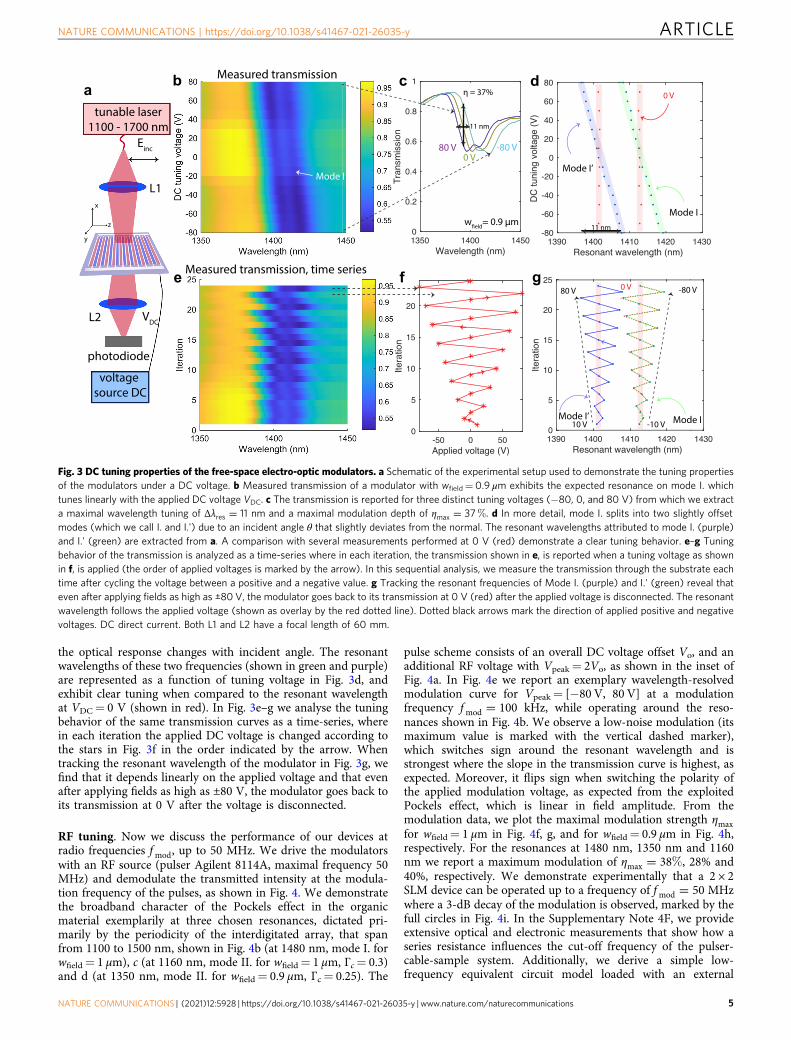
the optical response changes with incident angle. The resonantwavelengths of these two frequencies (shown in green and purple)are represented as a function of tuning voltage in Fig. 3d, andexhibit clear tuning when compared to the resonant wavelengthat VDC= 0 V (shown in red). In Fig. 3e–g we analyse the tuningbehavior of the same transmission curves as a time-series, wherein each iteration the applied DC voltage is changed according tothe stars in Fig. 3f in the order indicated by the arrow. Whentracking the resonant wavelength of the modulator in Fig. 3g, wefind that it depends linearly on the applied voltage and that evenafter applying fields as high as ±80 V, the modulator goes back toits transmission at 0 V after the voltage is disconnected.
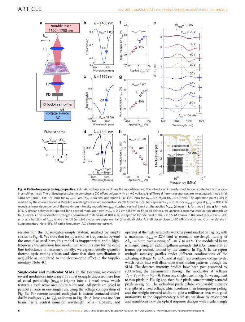
RF tuning. Now we discuss the performance of our devices atradio frequencies fmod, up to 50 MHz. We drive the modulatorswith an RF source (pulser Agilent 8114A, maximal frequency 50MHz) and demodulate the transmitted intensity at the modula-tion frequency of the pulses, as shown in Fig. 4. We demonstratethe broadband character of the Pockels effect in the organicmaterial exemplarily at three chosen resonances, dictated pri-marily by the periodicity of the interdigitated array, that spanfrom 1100 to 1500 nm, shown in Fig. 4b (at 1480 nm, mode I. forwfield= 1 μm), c (at 1160 nm, mode II. for wfield= 1 μm, Γc= 0.3)and d (at 1350 nm, mode II. for wfield= 0.9 μm, Γc= 0.25). The
pulse scheme consists of an overall DC voltage offset Vo, and anadditional RF voltage with Vpeak= 2Vo, as shown in the inset ofFig. 4a. In Fig. 4e we report an exemplary wavelength-resolvedmodulation curve for Vpeak= [−80 V, 80 V] at a modulationfrequency fmod ¼ 100 kHz, while operating around the reso-nances shown in Fig. 4b. We observe a low-noise modulation (itsmaximum value is marked with the vertical dashed marker),which switches sign around the resonant wavelength and isstrongest where the slope in the transmission curve is highest, asexpected. Moreover, it flips sign when switching the polarity ofthe applied modulation voltage, as expected from the exploitedPockels effect, which is linear in field amplitude. From themodulation data, we plot the maximal modulation strength ηmaxfor wfield= 1 μm in Fig. 4f, g, and for wfield= 0.9 μm in Fig. 4h,respectively. For the resonances at 1480 nm, 1350 nm and 1160nm we report a maximum modulation of ηmax ¼ 38%, 28% and40%, respectively. We demonstrate experimentally that a 2 × 2SLM device can be operated up to a frequency of fmod ¼ 50 MHzwhere a 3-dB decay of the modulation is observed, marked by thefull circles in Fig. 4i. In the Supplementary Note 4F, we provideextensive optical and electronic measurements that show how aseries resistance influences the cut-off frequency of the pulser-cable-sample system. Additionally, we derive a simple low-frequency equivalent circuit model loaded with an external
Fig. 3 DC tuning properties of the free-space electro-optic modulators. a Schematic of the experimental setup used to demonstrate the tuning propertiesof the modulators under a DC voltage. b Measured transmission of a modulator with wfield= 0.9 μm exhibits the expected resonance on mode I. whichtunes linearly with the applied DC voltage VDC. c The transmission is reported for three distinct tuning voltages (−80, 0, and 80 V) from which we extracta maximal wavelength tuning of Δλres ¼ 11 nm and a maximal modulation depth of ηmax ¼ 37%. d In more detail, mode I. splits into two slightly offsetmodes (which we call I. and I.') due to an incident angle θ that slightly deviates from the normal. The resonant wavelengths attributed to mode I. (purple)and I.' (green) are extracted from a. A comparison with several measurements performed at 0 V (red) demonstrate a clear tuning behavior. e–g Tuningbehavior of the transmission is analyzed as a time-series where in each iteration, the transmission shown in e, is reported when a tuning voltage as shownin f, is applied (the order of applied voltages is marked by the arrow). In this sequential analysis, we measure the transmission through the substrate eachtime after cycling the voltage between a positive and a negative value. g Tracking the resonant frequencies of Mode I. (purple) and I.' (green) reveal thateven after applying fields as high as ±80 V, the modulator goes back to its transmission at 0 V (red) after the applied voltage is disconnected. The resonantwavelength follows the applied voltage (shown as overlay by the red dotted line). Dotted black arrows mark the direction of applied positive and negativevoltages. DC direct current. Both L1 and L2 have a focal length of 60 mm.
NATURE COMMUNICATIONS | https://doi.org/10.1038/s41467-021-26035-y ARTICLE
NATURE COMMUNICATIONS | (2021) 12:5928 | https://doi.org/10.1038/s41467-021-26035-y | www.nature.com/naturecommunications 5
resistor for the pulser-cable-sample system, marked by emptycircles in Fig. 4i. We note that for operation at frequencies beyondthe ones discussed here, this model is inappropriate and a high-frequency transmission line model that accounts also for the cableline inductance is necessary. Finally, we experimentally quantifythermo-optic tuning effects and show that their contribution isnegligible as compared to the electro-optic effect in the Supple-mentary Note 4C.
Single-color and multicolor SLMs. In the following we combineseveral modulators into arrays: in a first example discussed here fourof equal periodicity (wfield= 1.4 μm) into a 4-pixel array, whichfeatures a total active area of 780 × 780 μm2. All pixels are poled inparallel at once in one single run, using the voltage configuration ofFig. 5a. For remote control, each pixel is instead contacted indivi-dually (voltages V1 to V4), as shown in Fig. 5b. A large area incidentbeam has a central emission wavelength of λ= 1154 nm, and
operates at the high-sensitivity working point marked in Fig. 5c, witha maximum ηmax ¼ 22% and a resonant wavelength tuning ofΔλres ¼ 5 nm over a swing of −40 V to 40 V. The modulated beamis imaged using an indium gallium arsenide (InGaAs) camera at 25frames per second, limited by the camera. In Fig. 5f–h, we reportmultiple intensity profiles under different combinations of theactuating voltages V1 to V4 and at eight representative voltage levels,which result into well discernible transmission patterns through theSLM. The depicted intensity profiles have been post-processed bysubtracting the transmission through the modulator at voltagesV1=V2=V3=V4= 0. From one single pixel in Fig. 5f, we augmentto two pixels in Fig. 5g and then four pixels concomitantly actuatedpixels in Fig. 5h. The individual pixels exhibit comparable intensitystrengths at a fixed voltage, which confirms their homogenous poling,and the straight-forward ability to pole a millimeter area with gooduniformity. In the Supplementary Note 4B, we show by experimentand simulations how the optical response changes with incident angle
Fig. 4 Radio-frequency tuning properties. a An AC voltage source drives the modulators and the introduced intensity modulation is detected with a lock-in amplifier. Inset: The utilized pulse scheme combines a DC offset voltage with an AC voltage. b–d Three different resonances are investigated: mode I. (at1480 nm) and II. (at 1160 nm) for wfield= 1 μm (hAu= 50 nm) and mode I. (at 1350 nm) for wfield= 0.9 μm (hAu= 40 nm). The operation point (OP) ismarked by the colored bullet. e Detailed wavelength-resolved modulation depth (solid vertical bar represents η= 25%) for wfield= 1 μm at fmod ¼ 100 kHzreveals a linear dependence of the maximum intensity modulation ηmax (dashed vertical bars) on the applied Vpeak (shown in f, for mode I. and g for modeII.)). A similar behavior is reported for a second modulator with wfield= 0.9 μm (shown in h). In all devices, we achieve a maximal modulation strength upto 30–40%. i The modulation strength (normalized to its value at 100 kHz) is reported for one pixel of the 2 × 2 SLM shown in the inset (scale bar = 200μm) as a function of fmod, where the full (empty) circles are experimental (analytical) data. A 3 dB decay close to 50 MHz is observed (further details inSupplementary Note 4F). RF radio frequency, AC alternating current.
ARTICLE NATURE COMMUNICATIONS | https://doi.org/10.1038/s41467-021-26035-y
6 NATURE COMMUNICATIONS | (2021) 12:5928 | https://doi.org/10.1038/s41467-021-26035-y | www.nature.com/naturecommunications
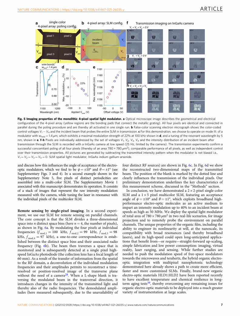
and discuss how this influences the angle of acceptance of the electro-optic modulators, which we find to be ϕ=±10° and θ=±1° (seeSupplementary Figs. 3 and 4). In a second example shown in theSupplementary Note 5, five pixels of distinct periodicities areassembled into a multi-color SLM. The Supplementary Movie 1associated with this manuscript demonstrates its operation. It consistsof a stack of images that represent the raw intensity modulationmeasured with the camera, while tuning the laser in resonance withthe individual pixels of the multicolor SLM.
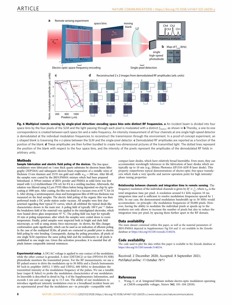
Remote sensing by single-pixel imaging. In a second experi-ment, we use our SLM for remote sensing on parallel channels.The core concept is that the SLM divides a three-dimensionalspace into n distinct space bins (here n= 4, the number of pixels),as shown in Fig. 6a. By modulating the four pixels at individualfrequencies (fmod;1 ¼ 100 kHz, fmod;2 ¼ 99 kHz, fmod;3 ¼ 98kHz, fmod;4 ¼ 97 kHz), a one-to-one correspondence is estab-lished between the distinct space bins and their associated radiofrequency (Fig. 6b). The beam then traverses a space that ismonitored and is subsequently detected at a single pixel high-speed InGaAs photodiode (the collection lens has a focal length of60 mm). As a result of the transfer of information from the spatialto the RF domain, a deconvolution of the individual modulationfrequencies and their amplitudes permits to reconstruct a time-resolved or position-resolved image of the transverse planewithout the need of a camera28. When a L-shape blank is tra-versing the modulated beam in the transversal direction, itintroduces changes in the intensity of the transmitted light andthereby also of the radio frequencies. The demodulated ampli-tudes (here measured subsequently, due to the unavailability of
four distinct RF sources) are shown in Fig. 6c. In Fig. 6d we showthe reconstructed two-dimensional maps of the transmittedbeam. The position of the blank is marked by the dotted line andclearly influences the transmission of the individual pixels. Ourpreliminary demonstration underlines the key characteristics ofthis measurement scheme, discussed in the “Methods” section.
In conclusion, we have demonstrated a 2 × 2-pixel single-colorSLM and a 1 × 5 pixel multicolor SLM, featuring an acceptanceangle of ϕ= ±10° and θ= ±1°, which exploits broadband high-performance electro-optic molecules as an active medium toimpart an intensity modulation up to 40% to an incident beam atspeeds as high as 50 MHz. We deploy the spatial light modulatorof total area of 780 × 780 μm2 in two real-life scenarios, for imageprojection and to remotely probe the environment on parallelchannels. The unique properties of the organic film, including theability to engineer its nonlinearity at will, at the nanoscale, itscompatibility with broad resonances (and thereby broadbandlasers), and its high-speed could open long-anticipated applica-tions that benefit from—or require—straight-forward up-scaling,simple fabrication and low power consumption: imaging, virtualreality, laser ranging, and sensing. While further studies areneeded to push the modulation speed of free-space modulatorstowards the microwaves and terahertz, the hybrid organic electro-optic integration with multipixel nanophotonic technologydemonstrated here already shows a path to create more efficient,faster and more customized SLMs. Finally, brand-new organicelectro-optic materials HLD1:HLD2 have been reported recentlyto have excellent temperature and chemical resilience in long-term aging tests39, thereby overcoming any remaining issues fororganic electro-optic materials to be deployed into a much greatervariety of instrumentation at large scales.
1150 1200
Wavelength (nm)
0.70
0.68Tra
nsm
issi
onpixel 1 pixel 2
pixel 3 pixel 4
a b
wire bonds
Vpol Vpol
incident beam
V1 V2
V3 V4Einc
100 μm
c
f
g
h80 V 60 V 40 V 20 V
-80 V-60 V-40 V-20 V
V3=80 V 60 V 40 V 20 V
-80 V-60 V-40 V-20 V
V1 = V2 = V4 = 0 V
V1 = V2 = V3= V4
V1 = V4 = 0 V
V3=80 V
V2=-80 V
60 V
-60 V -40 V -20 V
20 V
80 V
-80 V
60 V
-60 V
40 V
40 V
20 V
-20 V
-50 0 50
Offset voltage (V)
1155
1156
1157
1158
1159
1160
1161
Res
. wav
elen
gth
(nm
)
-100 0 100-20
-10
0
10
20
22%
d ew = 1.4 μm
III.
single color
0.00
-40 V
Transmission imaging on InGaAs camera
Applied Vpeak (V)
Max
. mod
ulat
ion
ηm
ax (
%)
Fig. 5 Imaging properties of the monolithic 4-pixel spatial light modulator. a Optical microscope image describes the geometrical and electricalconfiguration of the 4-pixel array (yellow regions are the bonding pads that connect the metallic grating). All four pixels are identical and connected inparallel during the poling procedure and are thereby all activated in one single run. b False-color scanning electron micrograph shows the color-codedcontrol voltages V1− V4 and the incident beam that probes the entire SLM in transmission. c For this demonstration, we choose to operate on mode III. of amodulator with wfield= 1.4 μm, which exhibits a maximal modulation strength of 22% at 100 kHz shown in d, and a tuning of the resonant wavelength by 5nm, shown in e. f–h Pixels are individually addressed by the set of voltages V1, V2, V3, V4 and the intensity distribution of an incident beam aftertransmission through the SLM is recorded with a InGaAs camera at low speed (25 Hz, limited by the camera). The transmission experiments confirm asuccessful concomitant poling of all four pixels (thereby of an area 780 × 780 μm2), comparable performance of all pixels, as well as independent controlover their transmission properties. All pictures are generated by subtracting the transmitted intensity pattern when the modulator is not biased i.e.,V1= V2= V3= V4= 0. SLM spatial light modulator, InGaAs indium gallium arsenide.
NATURE COMMUNICATIONS | https://doi.org/10.1038/s41467-021-26035-y ARTICLE
NATURE COMMUNICATIONS | (2021) 12:5928 | https://doi.org/10.1038/s41467-021-26035-y | www.nature.com/naturecommunications 7
MethodsSample fabrication and electric field poling of the devices. The free-spacemodulators were fabricated on 1mm thick quartz substrates by electron beam litho-graphy (ZEP520A) and subsequent electron beam evaporation of a metallic wires ofthickness 15 nm titanium and 25/35 nm gold and width wAu= 200 nm. After lift-off,the samples were coated by the JRD1:PMMA mixture which had been preparedbeforehand. A 50%wt mixture of JRD1 powder and PMMA in solid form was firstmixed with 1,1,2-trichlorethane (5% wt) for 8 h in a swirling machine. Afterwards, thesolution was filtered using 0.2 μm PTFE-filters before being deposited on-chip by spin-coating at 1000 rpm. After coating, the film was dried in a vacuum oven at 85 °C for 24h. After drying, a semitransparent, clean and homogenous film of 690 nm thickness wasmeasured on the final samples. The electric field poling of the organic film was thenperformed inside a DC probe station under vacuum. All samples were first char-acterized regarding their typical IV-curves, which all exhibited the typical diode-likecharacteristics shown in the main text. A poling field of typically 100V μm−1 (belowthe breakdown field of the material) was applied to the interdigitated electrodes, whichwere heated above glass temperature 97 °C. The poling field was kept for typically10 min at poling temperature, after which the samples were cooled down to roomtemperature. Finally, poled samples were inspected both in bright and dark fieldmicroscopy, as well as using atomic force microscopy. As shown, the film changesconformation quite significantly, which can be used as an indication of efficient poling.In the case of the multipixel SLMs, all pixels are contacted in parallel prior to electricfield poling by wire bonding. Consequently, during the poling procedure, all pixels ofone single SLM experience the same poling field and the nonlinearity in all pixels isestablished in one single run. Given this activation procedure, it is essential that allpixels feature comparable internal resistances.
Experimental setup. A DC/AC voltage is applied to one contact of the modulator,while the other contact is grounded. A slow (DET20C2) or fast (FPD310-FS-NIR)photodiode monitors the transmitted power. For the RF measurements, we use aRF pulsed source to drive the modulators up to 50 MHz and a Zurich InstrumentsRF lock-in amplifier (MFLI, 5 MHz and UHFLI, 600 MHz) to demodulate thetransmitted intensity at the modulation frequency of the pulses. We use a tunablelaser (super-K Select) to probe the modulation characteristics of our modulators.Its linewidth is described in detail in Fig. 4 of the Supplementary Information, andexceeds 4 nm and can range up to 11.5 nm. The ability of our modulators tointroduce significant intensity modulation even to a broadband incident beam arean experimental proof that the modulators are—in principle—compatible with
compact laser diodes, which have relatively broad linewidths. Even more, they canaccommodate wavelength tolerances in the fabrication of laser diodes which aretypically up to 10 nm (e.g., Eblana Photonics EP1310-ADF-B laser diode). Thisproperty outperforms typical demonstrations of electro-optic free-space transdu-cers which trade a very specific and narrow operation point for high intensity/phase tuning properties.
Relationship between channels and integration time in remote sensing. Thefrequency resolution of the individual channels is given by δf ¼ 1
tint, where tint is the
total integration time per pixel. A resolution around 0.1 kHz requires 10 msintegration time and is sufficient to resolve modulation frequencies spaced by 1kHz. In our case, the demonstrated modulation bandwidth up to 50 MHz wouldaccommodate—in principle—the modulation frequencies of 50,000 pixels. How-ever, having the ability to modulate the individual pixels at speeds up to theterahertz not only allows to increase the number of pixels but also to reduce theintegration time per pixel, by spacing them further apart in the RF domain.
Data availabilityThe main dataset contained within this paper, as well as the material parameters ofJRD1:PMMA depicted in Supplementary Fig S10 and 11 are available in the Zenododatabase at https://doi.org/10.5281/zenodo.5140234.
Code availabilityThe code used to plot the data within this paper is available in the Zenodo database athttps://doi.org/10.5281/zenodo.5140234.
Received: 2 December 2020; Accepted: 8 September 2021;
References1. Wang, C. et al. Integrated lithium niobate electro-optic modulators operating
at CMOS-compatible voltages. Nature 562, 101–104 (2018).
Fig. 6 Multipixel remote sensing by single-pixel detection: encoding space bins onto distinct RF frequencies. a An incident beam is divided into fourspace bins by the four pixels of the SLM and the light passing through each pixel is modulated with a distinct fmod,n, as shown in b Thereby, a one-to-onecorrespondence is created between each space bin and a radio-frequency. An intensity measurement of all four channels at one single high-speed detectoris demodulated at the individual modulation frequencies to reconstruct the transmission through the environment. In a proof-of-concept experiment, anL-shaped blank is traversing the x-z-plane between the SLM and the single-pixel detector. c Demodulated RF amplitudes are reported as a function of theposition of the blank. d These amplitudes are then further bundled to create two-dimensional pictures of the transmitted light. The dotted lines representthe position of the blank with respect to the four space bins, and the intensity of the pixels represent the amplitudes of the demodulated RF fields inarbitrary units.
ARTICLE NATURE COMMUNICATIONS | https://doi.org/10.1038/s41467-021-26035-y
8 NATURE COMMUNICATIONS | (2021) 12:5928 | https://doi.org/10.1038/s41467-021-26035-y | www.nature.com/naturecommunications

2. Abel, S. et al. Large pockels effect in micro- and nanostructured bariumtitanate integrated on silicon. Nat. Mater. 18, 42–47 (2019).
3. Haffner, C. et al. All-plasmonic Mach-Zehnder modulator enabling opticalhigh-speed communication at the microscale. Nat. Photonics 9, 525–528(2015).
4. Benea-Chelmus, I.-C. et al. Electro-optic interface for ultrasensitive intracavityelectric field measurements at microwave and terahertz frequencies. Optica 7,498–505 (2020).
5. Benea-Chelmus, I.-C., Settembrini, F. F., Scalari, G. & Faist, J. Electric fieldcorrelation measurements on the electromagnetic vacuum state. Nature 568,202–206 (2019).
6. Wu, P. C. et al. Dynamic beam steering with all-dielectric electro-optic III-Vmultiple-quantum-well metasurfaces. Nat. Commun. 10, 3654 (2019).
7. Fan, L. et al. Superconducting cavity electro-optics: a platform for coherentphoton conversion between superconducting and photonic circuits. Sci. Adv.4, 4994 (2018).
8. Riemensberger, J. et al. Massively parallel coherent laser ranging using asoliton microcomb. Nature 581, 164–170 (2020).
9. Barredo, D., de Léséleuc, S., Lienhard, V., Lahaye, T. & Browaeys, A. An atom-by-atom assembler of defect-free arbitrary two-dimensional atomic arrays.Science 354, 1021–1023 (2016).
10. Schwarz, B. Mapping the world in 3D. Nat. Photonics 4, 429–430 (2010).11. Dudley, D., Duncan, W., & Slaughter, J. Emerging Digital micromirror device
(DMD) applications. DLPTM Products New Appl. 4985, 14–23 (2003).12. Hu, L. et al. Phase-only liquid-crystal spatial light modulator for wave-front
correction with high precision. Opt. Express 12, 6403–6409 (2004).13. Smolyaninov, A., El Amili, A., Vallini, F., Pappert, S. & Fainman, Y.
Programmable plasmonic phase modulation of free-space wavefronts atgigahertz rates. Nat. Photonics 13, 431–435 (2019).
14. Khorasaninejad, M. & Capasso, F. Metalenses: versatile multifunctionalphotonic components. Science 358, eaam8100 (2017).
15. Balthasar Mueller, J. P., Rubin, N. A., Devlin, R. C., Groever, B. & Capasso, F.Metasurface polarization optics: independent phase control of arbitraryorthogonal states of polarization. Phys. Rev. Lett. 118, 113901 (2017).
16. Chen, W. T., Zhu, A. Y. & Capasso, F. Flat optics with dispersion-engineeredmetasurfaces. Nat. Rev. Mater. 5, 604–620 (2020).
17. Tittl, A. et al. Imaging-based molecular barcoding with pixelated dielectricmetasurfaces. Science 360, 1105–1109 (2018).
18. Gao, B. et al. Lithium niobate metasurfaces. Laser Photonics Rev. 13, 1800312(2019).
19. Weigand, H. et al. Enhanced electro-optic modulation in resonantmetasurfaces of lithium niobate. https://arXiv.org/2106.12232v2.
20. Karvounis, A. et al. Electro-optic metasurfaces based on barium titanatenanoparticle films. Adv. Optical Mater. 8, 2000623 (2020).
21. Li, S.-Q. et al. Phase-only transmissive spatial light modulator based ontunable dielectric metasurface. Science 364, 1087–1090 (2019).
22. Shirmanesh, G. K., Sokhoyan, R., Wu, P. C. & Atwater, H. A. Electro-opticallytunable multifunctional metasurfaces. ACS Nano 14, 6912–6920 (2020).
23. Peng, C., Hamerly, R., Soltani, M. & Englund, D. R. Design of high-speedphase-only spatial light modulators with two-dimensional tunable microcavityarrays. Opt. Express 27, 30669–30680 (2019).
24. Forouzmand, A., Salary, M. M., Inampudi, S. & Mosallaei, H. A tunablemultigate indium-tin-oxide-assisted all-dielectric metasurface. Adv. OpticalMater. 6, 1701275 (2018).
25. Huang, Y.-W. et al. Gate-tunable conducting oxide metasurfaces. Nano Lett.16, 5319–5325 (2016).
26. Reshef, O., De Leon, I., Alam, M. Z. & Boyd, R. W. Nonlinear optical effects inepsilon-near-zero media. Nat. Rev. Mater. 4, 535–551 (2019).
27. Park, J. et al. All-solid-state spatial light modulator with independent phaseand amplitude control for three-dimensional LiDAR applications. Nat.Nanotechnol. https://doi.org/10.1038/s41565-020-00787-y (2020).
28. Zeng, B. et al. Hybrid graphene metasurfaces for high-speed mid-infrared lightmodulation and single-pixel imaging. Light Sci. Appl. 7, 51 (2018).
29. Abdollahramezani, S. et al. Tunable nanophotonics enabled by chalcogenidephase-change materials. Nanophotonics 9, 1189–1241 (2020).
30. Michel, A.-K. U. et al. Optical properties of amorphous and crystalline GeTenanoparticle thin films: a phase-change material for tunable photonics. ACSAppl. Nano Mater. 3, 4314–4320 (2020).
31. Chaudhary, K. et al. Polariton nanophotonics using phase-change materials.Nat. Commun. 10, 4487 (2019).
32. Leitis, A. et al. All-dielectric programmable Huygens’ metasurfaces. Adv.Funct. Mater. 30, 1910259 (2020).
33. Wang, Q. et al. Optically reconfigurable metasurfaces and photonic devicesbased on phase change materials. Nat. Photonics 10, 60–65 (2016).
34. Arbabi, E. et al. MEMS-tunable dielectric metasurface lens. Nat. Commun. 9,812 (2018).
35. She, A., Zhang, S., Shian, S., Clarke, D. R. & Capasso, F. Adaptive metalenseswith simultaneous electrical control of focal length, astigmatism, and shift. Sci.Adv. 4, eaap9957 (2018).
36. Berto, P. et al. Tunable and free-form planar optics. Nat. Photonics 13,649–656 (2019).
37. Heni, W. et al. Nonlinearities of organic electro-optic materials in nanoscaleslots and implications for the optimum modulator design. Opt. Express 25,2627–2653 (2017).
38. Salamin, Y. et al. Compact and ultra-efficient broadband plasmonic terahertzfield detector. Nat. Commun. 10, 5550 (2019).
39. Xu, H. et al. Ultrahigh electro-optic coefficients, high index of refraction, andlong-term stability from Diels-Alder cross-linkable binary molecular glasses.Chem. Mater. 32, 1408–1421 (2020).
40. Koch, U. et al. A monolithic bipolar CMOS electronic-plasmonic high-speedtransmitter. Nat. Electron. 3, 338–345 (2020).
41. Zhang, J. et al. Electrical tuning of metal-insulator-metal metasurface withelectro-optic polymer. Appl. Phys. Lett. 113, 231102 (2018).
42. Zhang, J., Kosugi, Y., Otomo, A., Nakano, Y. & Tanemura, T. Activemetasurface modulator with electro-optic polymer using bimodal plasmonicresonance. Opt. Express 25, 30304 (2017).
43. Greenlee, C. et al. Electro-optic polymer spatial light modulator based on aFabry–Perot interferometer configuration. Opt. Express 19, 12750–12758 (2011).
44. Dalton, L. R., Sullivan, P. A. & Bale, D. H. Electric field poled organic electro-optic materials: state of the art and future prospects. Chem. Rev. 110, 25–55(2010).
45. Wang, S. S. & Magnusson, R. Theory and applications of guided-moderesonance filters. Appl. Opt. 32, 2606–2613 (1993).
46. Jin, W. et al. Benzocyclobutene barrier layer for suppressing conductance innonlinear optical devices during electric field poling. Appl. Phys. Lett. 104,243304 (2014).
AcknowledgementsThe authors acknowledge insightful discussions with Stefan Breuer, Christopher Bonzon,Dmitry Kazakov, Daniel Lim, Sydney Mason, Marcus Ossiander, and Noah Rubin, aswell as Zurich Instruments who lended the UHFLI. I.-C. Benea-Chelmus acknowledgessupport through the Swiss National Science Foundation for the postdoctoral fellowshipP2EZP2.181935 and an independent research grant from the Hans Eggenberger foun-dation. M.L. Meretska is supported by NWO Rubicon Grant 019.173EN.010, by theDutch Funding Agency NWO. D.L. Elder and L.R. Dalton acknowledge support from theAir Force Office of Scientific Research (FA9550-19-1-0069). Additionally, financialsupport from the Office of Naval Research (ONR) MURI program, under grant no.N00014-20-1-2450 is acknowledged. This work was performed in part at the HarvardUniversity Center for Nanoscale Systems (CNS); a member of the National Nano-technology Coordinated Infrastructure Network (NNCI), which is supported by theNational Science Foundation under NSF award no. ECCS-2025158. The electro-opticmolecules were synthesised in the Chemistry Department at the University ofWashington.
Author contributionsI.-C.B.-C. conceived, designed and implemented the experiments and wrote the manu-script with feedback from the other co-authors. I.-C.B.-C, M.M. and M.T. fabricated thesamples. I.-C.B.-C. did the theoretical derivations and the simulations. D.E. and L.D.developed the electro-optic molecules, measured the refractive indices and assisted withthe poling of the devices. I.-C.B.-C., M.M., M.T., and F.C. analysed the data. All authorsgave feedback to the manuscript.
Competing interestsA provisional patent application with U.S. Serial No.: 63/148,595 has been filed on thesubject of this work by the President and Fellows of Harvard College.
Additional informationSupplementary information The online version contains supplementary materialavailable at https://doi.org/10.1038/s41467-021-26035-y.
Correspondence and requests for materials should be addressed to Ileana-CristinaBenea-Chelmus or Federico Capasso.
Peer review information Nature Communications thanks Hyuck Choo and theanonymous reviewer(s) for their contribution to the peer review of this work.
Reprints and permission information is available at http://www.nature.com/reprints
Publisher’s note Springer Nature remains neutral with regard to jurisdictional claims inpublished maps and institutional affiliations.
NATURE COMMUNICATIONS | https://doi.org/10.1038/s41467-021-26035-y ARTICLE
NATURE COMMUNICATIONS | (2021) 12:5928 | https://doi.org/10.1038/s41467-021-26035-y | www.nature.com/naturecommunications 9

Open Access This article is licensed under a Creative CommonsAttribution 4.0 International License, which permits use, sharing,
adaptation, distribution and reproduction in any medium or format, as long as you giveappropriate credit to the original author(s) and the source, provide a link to the CreativeCommons license, and indicate if changes were made. The images or other third partymaterial in this article are included in the article’s Creative Commons license, unlessindicated otherwise in a credit line to the material. If material is not included in thearticle’s Creative Commons license and your intended use is not permitted by statutoryregulation or exceeds the permitted use, you will need to obtain permission directly fromthe copyright holder. To view a copy of this license, visit http://creativecommons.org/licenses/by/4.0/.
© The Author(s) 2021
ARTICLE NATURE COMMUNICATIONS | https://doi.org/10.1038/s41467-021-26035-y
10 NATURE COMMUNICATIONS | (2021) 12:5928 | https://doi.org/10.1038/s41467-021-26035-y | www.nature.com/naturecommunications