high power pin diodes - skyworks · high power pin diodes description skyworks’ smp1324-087lf,...
TRANSCRIPT

Applications• Series/shunt elements
in high power HF/VHF/UHF transmit/receive (T/R) switches
Features • Very low thermal
resistance for excellent power handling: 40 W C/W typical
• Low series resistance – SMP1324-087LF:
0.4 W @ 50 mA – SMP1371-087LF:
0.5 W @ 10 mA – SMP1302-085LF:
1.5 W @ 100 mA
• Suitable as series elements in high power switches
– SMP1324-087LF: 35 W CW
– SMP1371-087LF: 23 W CW
– SMP1345-087LF: 10W CW
• Suitable as shunt elements in high power switches
– SMP1302-085LF: 50 W CW
• Excellent distortion performance
• Lead (Pb)-free, RoHS-compliant, Green™ QFN 2 x 2 mm packages
• ESD Class 1 C, human body model
Skyworks Green™ products are compliant with all applicable materials leg-islation and are halogen-free. For additional information, refer to Skyworks Definition of Green™, document number SQ04-0074.
High Power PIN DiodesDescriptionSkyworks’ SMP1324-087LF, SMP1371-087LF and SMP1302-085LF PIN diodes are designed for use in high-power-handling switches from 1–900 MHz. SMP1324-087LF and SMP1371-087LF are optimized for use as series diodes. SMP1302-085LF is optimized for use as a shunt diode. Due to their thermally-enhanced package designs, these diodes have very low thermal resistance which enables them to handle very large input power.
The SMP1345-087LF is ideally suited for use as a high isolation, series switching element. The SMP1345-087LF has a 10 micron nominal I layer thickness, which enables it to switch impedance very rapidly while handling large input signals, when the exposed paddle of the diode is connected to a printed circuit board which provides an adequately large thermal conductance to a heatsink to maintain the die temperature to be less than 150 °C. Minority carrier lifetime is 100 ns typical, series resistance at 10 mA bias current is 1.5 Ω typical and total capacitance is less than 0.2 pF maximum.
The SMP1371-087LF has a 12 micron nominal I layer thickness, which enables it to handle input signals up to 23 W CW when the device is mounted as a series element in a switch built on a printed circuit board which has a relatively high thermal conductance, such as Rogers 5880. In the identical circuit constructed on FR4 printed circuit board material the maximum input power is 20 W CW. Minority carrier lifetime is 200 ns minimum, series resistance at 10 mA bias current is 0.5 Ω maximum and total capacitance is 0.9 pF typical. The SMP1371-087LF is rated to dissipate 2 W maximum.
The SMP1324-087LF has a 100 micron nominal I layer thickness, which enables it to handle input signals up to 35 W CW when the device is mounted as a series element in a switch built on a printed circuit board which has a relatively high thermal conductance, such as Rogers 5880. In the identical circuit constructed on FR4 printed circuit board material the maximum input power is 30 W CW. Minority carrier lifetime is 6 µs typical, series resistance at 50 mA bias current is 0.4 Ω typical and total capacitance is 0.9 pF typical. The SMP1324-087LF is rated to dissipate 2 W maximum.
The SMP1302-085LF is ideally suited for use as a shunt switching element. The SMP1302-085LF has a 50 micron nominal I layer thickness, which enables it to handle input signals as large as 50 W CW when the exposed paddle of the diode is connected to a printed circuit board which provides an adequately large thermal conductance to a heat sink to maintain the die temperature to be less than 150 °C. Minority carrier lifetime is 700 ns typical, series resistance at 100 mA bias current is 1 Ω typical and total capacitance is less than 0.3 pF.
Design information for high power switches may be found in the Skyworks Application Note, Design with PIN Diodes, document number 200312.

SMP1324-087LF Electrical Characteristics
SMP1324-087LF Typical Performance Data @ 25 °C (Unless Otherwise Noted)
SMP1324-087LF Absolute Maximum Ratings
SMP1324-087LF Electrical Specifications1 (TA = +25 °C, Unless Otherwise Noted)
Capacitance vs. Reverse Voltage @ 1 MHz Series Resistance vs. Forward Current @ 100 MHz
Parameter Symbol Min. Max. Units
Forward current IF – 200 mA
Dissipated power @ 25 °C PD – 2 W
Operating temperature TA –55 +85 °C
Storage temperature TSTG –55 +200 °C
Junction temperature TJ –55 +175 °C
Parameter Symbol Test Condition Min. Typ. Max. Units
Forward voltage VF IF = 50 mA – 0.9 1.2 V
Reverse leakage current IR VR = 200 V – 10 μA
Series resistance RS IF = 50 mA, f = 100 MHz – 0.40 0.75 W
Total capacitance CT0 CT30
VR = 0 V, f = 100 MHz VR = 30 V, f = 1 MHz
– 0.9 0.9
1.5 1.5
pF pF
Minority carrier lifetime TL IF = 10 mA 2 6 – μs
Parallel resistance RP VR = 0 V, f = 100 MHz 5 6 – kW
I region width W – – 100 – μm
Note 1: Performance is guaranteed only under the conditions listed in this Table.
0
1
2
3
4
5
0 5 10 15 20 25 30
Reverse Voltage (V)
Capa
cita
nce
(pF)
0.1
100
10
1.0
1.00.1 10 100
Forward Current (mA)
Serie
s Re
sist
ance
(Ω)
Package CharacteristicsThe 087LF package is a 2 x 2 x 0.9 mm surface mount QFN package with an exposed paddle. The die is mounted directly onto this solid metal paddle, which provides a very low thermal resistance path from the die to the environment external to the die. This low thermal resistance permits the die to maintain low junction temperature when dissipating significant power, thereby enabling the die to handle high power input signals.
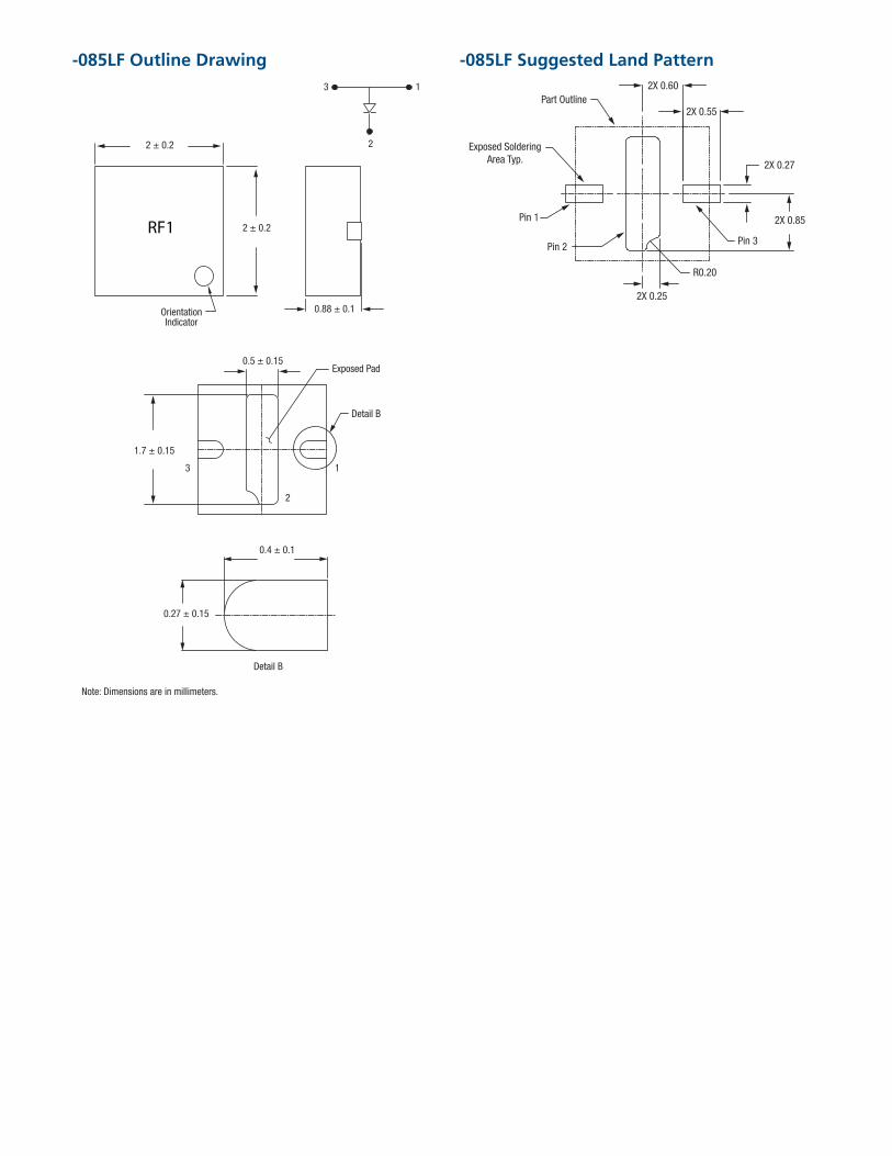
The 085LF package is a 2 x 2 x 0.9 mm, surface mount plastic package. This package has three terminals, one of which is an exposed paddle which is the cathode contact, the remaining two of which are each connected to the anode of the diode. The exposed paddle provides a very low thermal resistance path from the cathode of the diode to the environment external to the die. The two anode contacts are situated on opposite sides of the exposed paddle, which is optimal for connecting two transmission line sections together via a shunt PIN diode.

SMP1371-087LF Typical Performance Data @ 25 °C (Unless Otherwise Noted)
SMP1371-087LF Electrical Characteristics
SMP1371-087LF Absolute Maximum Ratings
SMP1371-087LF Electrical Specifications1 (TA = +25 °C, Unless Otherwise Noted)
Series Resistance vs. Forward Current Capacitance vs. Reverse Voltage @ 1 MHz
Parameter Symbol Min. Max. Units
Forward current IF – 200 mA
Reverse voltage VR 35 V
Dissipated power @ 25 °C PD – 2 W
Operating temperature TA –40 +85 °C
Storage temperature TSTG –55 +200 °C
Junction temperature TJ –55 +175 °C
Parameter Symbol Test Condition Min. Typ. Max. Units
Forward voltage VF IF = 50 mA – – 1.0 V
Reverse leakage current IR VR = 35 V – – 10 μA
Series resistance RS IF = 10 mA, f = 100 MHz – – 0.5 W
Total capacitance CT20 VR = 20 V, f = 1 MHz – – 1.2 pF
Minority carrier lifetime TL IF = 10 mA 200 – – μs
Parallel resistance RP VR = 0 V, f = 100 MHz 2.5 – – kW
I region width W – – 12 – μm
Note 1: Performance is guaranteed only under the conditions listed in this Table.
0.1
1
10
0.1 1 10 100
Forward Current (mA)
Serie
s Re
sist
ance
(Ohm
s)
0
0.4
0.8
1.2
1.6
2
0 5 10 15 20 25 30
Reverse Voltage (V)
Capa
cita
nce
(pF)

SMP1302-085LF Electrical Characteristics
Parameter Symbol Condition Min. Typ. Max. Unit
Reverse current IR VR = 200 V – – 10 µA
Capacitance CT30 VR = 30 V, f = 1 MHz – – 0.3 pF
Resistance RS10 IF = 10 mA, f = 100 MHz – – 3 W
Resistance RS100 IF = 100 mA, f = 100 MHz – 1.0 1.5 W
Forward voltage VF IF = 10 mA – 0.8 – V
Carrier lifetime TL IF = 10 mA – 700 – ns
I-Region width W – 50 – µm
CW thermal resistance QJC– 40 °C/W
Pulse thermal resistance QPSingle 1 µs pulse – 3.5 – °C/W
Performance is guaranteed only under the conditions listed in the specifications table and is not guaranteed under the full range(s) described by the Absolute Maximum specifications.Exceeding any of the absolute maximum/minimum specifications may result in permanent damage to the device and will void the warranty.
SMP1302-085LF Absolute Maximum Ratings
SMP1302-085LF Electrical Specifications (TA = +25 °C, Unless Otherwise Noted)
Parameter Symbol Min. Max. Unit
Reverse voltage VR – 200 V
Forward current at 25 °C IF – 200 mA
CW power dissipation at 25 °C PD – 3 W
1 µs pulse power dissipation PD – 30 W
Storage temperature range TSTORE –65 +200 °C
Operating temperature range TOP –40 +150 °C

Series Resistance vs. Current @ 100 MHz
0.01 0.1 1 10 100
Forward Current (mA)
Serie
s Re
sist
ance
(W)
0.1
1
10
100
1000
0 1 2 5 10 20 10050
Capacitance vs. Reverse Voltage
0
0.2
0.4
0.6
0.1
0.3
0.5
0.7
0.8
Reverse Voltage (V)
Capa
cita
nce
(pF)
100 MHz
1 MHz
1 GHz
SMP1302-085LF Typical Performance Data @ 25 °C (Unless Otherwise Noted)
Typical Pulse Thermal Impedance
0
5
10
15
20
25
30
35
1 10 100 1000
Pulse Width (µs)
Puls
e Th
erm
al Im
peda
nce
(°C/
W)
Series Resistance vs. Current @ 100 MHz Capacitance vs. Reverse Voltage
Typical Pulse Thermal Impedance

Parameter Symbol Condition Min. Typ. Max. Unit
Reverse current IR VR = 50 V – – 10 µA
Capacitance CT5 VR = 5 V, f = 1 MHz – 0.16 0.2 pF
Resistance RS1 IF = 1 mA, f = 100 MHz – 3.5 – W
Resistance RS10 IF = 10 mA, f = 100 MHz – 1.5 2.0 W
Forward voltage VF IF = 10 mA – 0.89 – V
Carrier lifetime TL IF = 10 mA – 100 – ns
I-Region width W – 10 – µm
CW thermal resistance QJC– 45 °C/W
Pulse thermal resistance QPSingle 1 µs pulse – 4.0 – °C/W
Performance is guaranteed only under the conditions listed in the specifications table and is not guaranteed under the full range(s) described by the Absolute Maximum specifications.Exceeding any of the absolute maximum/minimum specifications may result in permanent damage to the device and will void the warranty.
SMP1345-087LF Absolute Maximum Ratings
SMP1345-087LF Electrical Specifications (TA = +25 °C, Unless Otherwise Noted)
Parameter Symbol Min. Max. Unit
Reverse voltage VR – 50 V
Forward current at 25 °C IF – 200 mA
CW power dissipation at 25 °C PD – 3 W
1 µs pulse power dissipation PD – 30 W
Storage temperature range TSTORE –65 +200 °C
Operating temperature range TOP –55 +150 °C
SMP1345-087LF Electrical Characteristics
Reverse Voltage (V)
Capa
cita
nce
(pF)
0 5 10 15 2520 300.05
0.10
0.15
0.20
0.01 0.1 1 10 100
Forward Current (mA)
Serie
s Re
sist
ance
(Ω)
0.01
0.1
1
10
100
Series Resistance vs. CurrentCapacitance vs. Reverse Voltage

-2.0
-1.8
-1.6
-1.4
-1.2
-1.0
-0.8
-0.6
-0.4
-0.2
0
0.1 0.2 0.3 0.4 0.5 0.6 0.7 0.8 0.9 1.0
Frequency (GHz)
Inse
rtion
Los
s (d
B)
Tx IN to ANT Insertion Loss State
ANT to Rx OUT Insertion Loss State
-60-55-50-45-40-35-30-25-20-15-10
-50
0.1 0.2 0.3 0.4 0.5 0.6 0.7 0.8 0.9 1.0
Frequency (GHz)
Isol
atio
n (d
B)
ANT to Tx IN Isolation
ANT to Rx OUT Isolation
Typical Pulse Thermal ImpedanceForward Voltage vs. Forward Current
High Power T/R Switch Design ApplicationsTwo SPDT T-R switches were fabricated utilizing PIN diodes, as shown in the schematic diagram below. Both switches utilize a single, series PIN diode on the transmit side of the switch, as well as a series-shunt PIN diode pair on the receive side of the switch. One of the switches contains SMP1324-087LF PIN diodes in the series diode positions. The other switch has SMP1371-087LF PIN diodes in these positions. Both switch assemblies use an SMP1302-085LF in the shunt position on the receive side of the switch.
Power HandlingThese switches were each built using two different printed circuit board (PCB) substrates: Rogers 5880 and FR4, each of which had dielectric thickness of 0.010 inches. The bottom-most layer of each PCB assembly was FR4 material of approximately 0.052 inches thickness, utilized as a carrier and PCB stiffener. Both types of PCBs had metal heat sinks attached to their undersides.
With the Rogers 5880 PCBs, the switches were subjected to the power levels listed below for the durations also listed below, with no degradation:
For the PCBs entirely comprising FR4, these power levels were as shown below, due to the higher thermal resistance of the FR4.
Part Number Incident Power Duration
SMP1324-087LF 35 W 24 hours
SMP1371-087LF 23 W 24 hours
Part Number Incident Power Duration
SMP1324-087LF 35 W 24 hours
SMP1371-087LF 23 W 24 hours

T/R Switch Circuit Diagram
R = 300 Ω
L = 560 nHL = 560 nH
C = 1000 pF C = 1000 pF
±I BIAS
Tx Input Rx Output
SMP1302-085 LF
SMP1324-087LFor
SMP1371-087LF2 plcs
C = 1000 pF
Antenna
±I BIAS
C = 0.1 µF
C = 0.1 µF
L = 560 nH
Port 1
Port 2Port 3

-087LF Outline Drawing
S1989
2Pin 1Indicator
0.90 ± 0.1
Detail A
0.4 ± 0.1
0.30 ± 0.05
Exposed Pad
2 1
2 1
Detail A
1.15 + 0.1/–0.15
0.20 Min. 0.20
1.6 + 0.1/–0.15
Top View Side View Bottom View
2
0.05 C2X
0.05 C2X 0.08 C
2X 3
5
0.10 C
AB
C
Seating Plane
0.0 – 0.05
All measurements are in millimeters.Dimensioning and tolerancing according to ASME Y14.5M-1994.Coplanarity applies to the exposed heat sink slug as well as the terminals..Dimension applies to metalized terminal and is measured between 0.10 mm and 0.30 mm from terminal tip.
0.10 M C A B
-087LF Suggested Land Pattern
0.25
2X 0.80
0.55
0.800.35
Pin 2Pin 1
Part Outline
Exposed SolderingArea, Typical
S1988
-085LF Suggested Land Pattern
Pin 3Pin 2
Part Outline
2X 0.27
R0.20
Exposed SolderingArea Typ.
Pin 1
2X 0.55
2X 0.60
2X 0.85
2X 0.25
-085LF Outline Drawing
Note: Dimensions are in millimeters.
2 ± 0.2
2 ± 0.2
OrientationIndicator
0.88 ± 0.1
Detail B
0.4 ± 0.1
0.27 ± 0.15
3
3 1
2
Exposed Pad
Detail B
0.5 ± 0.15
1.7 ± 0.15
1
2
RF1

Application Notes For additional information, please refer to the following Application Notes.
Solder Reflow Information
Discrete Devices and IC Switch/Attenuators Tape and Reel Package Orientation
Design with PIN Diodes
Through our Green Initiative,™ we are committed to manufacturing products that comply with global government directives and industry requirements.
Skyworks is continuously innovating RF, analog and mixed-signal ICs. For the latest product introductions and information about Skyworks, visit our Web site at www.skyworksinc.com
For additional information on our broad overall product portfolio, please contact your local sales office or email us at [email protected].
Green Initiative™
BrochuresRF Diode Design Guide
Published ArticlesRF/Microwave Solid State Switches: Part 1
Solid State RF/Microwave Switch Technology: Part 2
PIN Diodes for High Power T/R Switches

Skyworks Solutions, Inc.20 Sylvan Road, Woburn, MA 01801USA: (781) 376-3000 • Asia: 886 2 2735 0399Europe: 33 (0)1 43548540 • Fax: (781) 376-3100Email: [email protected] • www.skyworksinc.com
BRO399-11A 5/11 Printed on Recycled Paper.