high power factor offline flyback controller al1788ev1user ... · high power factor offline flyback...
TRANSCRIPT

High Power Factor Offline Flyback Controller AL1788EV1User Guide
AL1788 EV1 Draft 0.2 Page 1 of 19 August 23, 2017 www.diodes.com
General Description
The AL1788 is a high performance high Power Factor Corrected (PFC) LED driver controller. It is a Primary Side controller designed for driving the Flyback converter. Based on Valley-ON Quasi-resonant mode, AL1788 is operating at Boundary Conduction Mode (BCM) which is good for EMI. It is universal Flyback solution with high PF and low THD.
The AL1788EV1 is designed to serve as an example for dual-CV (Constant Voltage) Output where main CV output requires high PFC and a secondary CV output is for wireless connectivity.
Key Features
Input Voltage Range: 8.0V to 25V
Primary Side Control or Secondary Side Control (No Opto Coupler required) AC-to-CV Regulation
Valley-on function to achieve low switching loss
High Power Factor (PF) and Low Total Harmonic Distortion (THD) for wide Loading range
High Efficiency
Low system BOM cost
Low Standby Power
Under Voltage Lockout (UVLO)
Over Voltage Protection (OVP)
Over Current Protection (OCP)
Output Short Protection (OSP)
Over-temperature protection (OTP): Thermal shutdown and auto thermal recovery
Application:
High PFC and low THD power supply
Smart Connected LED Light Bulbs
Smart Connected LED Tubes, Panel Lights, Troffers and Ceiling Lights
AL1788EV1 Board Specifications
Parameter Value
Input Voltage 100Vac to 240VAC
Power Rating 32Watt
Main output: (Vout / Io)
CV1: VO1 - 42V / 750mA
CV2: 3V3 - 3.3V / 200mA
Standby Power <500 mW (No Load on CV1, 15mA for CV2)
Protections UVLO, OVP, OSP, OLP, OTP
Efficiency >87% for Vo1 Full Load
XYZ Dimension 14.5 x 45 x 35 mm
Application
1-Channel Dimmable White 2-Channel Tunable White Smart Lightning dual CV-output power
Evaluation Board View:
Figure 1: Top View
Figure 2: Bottom View
AL1788

High Power Factor Offline Flyback Controller AL1788EV1 User Guide
AL1788EV1 Draft 0.2 Page 2 of 19 August 23, 2017 www.diodes.com
AL1788 Pin Assignment
1
2
3
6
4
Out
COMP
GND 5 Vcc
FB
CS
Top View (SOT26)
Pin Name Pin Number Descriptions
CS 1 Primary Current Sensing
GND 2 Ground
COMP 3 Loop Compensation Pin
FB 4 Voltage Sensing Feedback
VCC 5 Power Supply
OUT 6 Gate Driver Output
Evaluation Board Schematic
Figure 3: Evaluation Board Schematic
RX6NA
VO1
3V3
D34NA
RX1
NA
CON2 2P-2.54mm
12
R04200K
R151K
N
VO2
R17NA
VO2
C080.1uF
D01RS1M
R01750K
GND2
D33NA
3V3GND
C05
470PF
CY12200pF
C072.2uF
R06180K
GND3
+ C32
470uF
GND
R14NA
VO2
L02 222
FS1T2.0A-250V
R6316K
L
C51
NA
GND
VO1
RX3 NA
RX5NA RX4 NA
T01BPQ2625(0.41mH)
1
5.6
4
3
11,12
7,8
9
10
GND
R10
0RC62100nF
C010.33uF
CX1 NA
R61100K
R521K
R31
100R
R51
NA
R110R3
R6249.9K
C642.2uF
L614.7uH
R08
22R
C611uf
C32A22K
R0711.5K
+ C33
470uFL03 222
R16324K
C020.47uF
D044148W
R132R2
R120R3
GND1
D61SBR1A40S
U61AP3211
5
2
4 3
6
1
VIN
GN
D
EN FB
SWBS
U01 AL1788
1
2
3 4
5
6CS
GND
COMP FB
VCC
OUT
C63
0.1uF
CON3 2P-2.54mm
12
R0951K
C06NA
R05200K
RX2
NA
Q01DMG9N65
R03
10R
D31
UF5JD1
C090.1uF
C31
68PF
L01UU10.5/12mH
14
23
+ C52200uF/35V
+C0447uF
+C032.2uF
CON1 2P-2.54mm
12
D02
RS1MSWF
CX2NA
VR1470V
+-~
~
BD1KBP206G
2
1
3
4
D034148W
R02750K
D32
NA
D51
DFLS1100
High Power Factor Offline Flyback Controller AL1788EV1 User Guide
AL1788EV1 Draft 0.2 Page 3 of 19 August 23, 2017 www.diodes.com
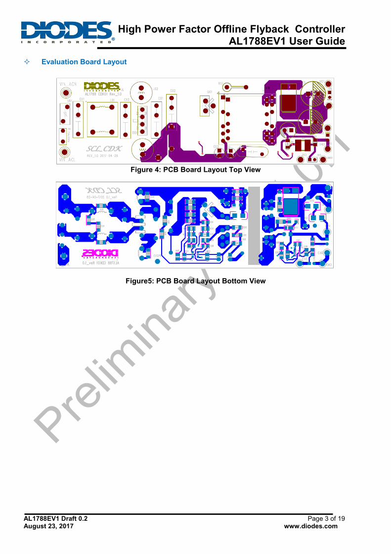
Evaluation Board Layout
Figure 4: PCB Board Layout Top View
Figure5: PCB Board Layout Bottom View

High Power Factor Offline Flyback Controller AL1788EV1 User Guide
AL1788EV1 Draft 0.2 Page 4 of 19 August 23, 2017 www.diodes.com
Bill of Material (BOM)
# Name QTY Part Number Description Note
1 U01 1 AL1788W6-7 Single-Stage Flyback and PFC controller for CV regulation (SOT236)
Diodes, Inc.
2 U61 1 AP3211 1.4MHz, 1.5A Asynchronous DC-DC buck converter (SOT236)
Diodes, Inc.
3 D01 1 RS1M 1.0A surface mount fast recovery rectifier (SMA)
Diodes, Inc.
4 D02 1 RS1MSWF 1.0A surface mount fast recovery rectifier (SOD123F)
Diodes, Inc.
5 D03,D04 2 1N4148W Surface mount fast switching diode (SOD123)
Diodes, Inc.
6 D31 1 UF5JD1 5A ULTRA-FAST rectifier (TO252) Diodes, Inc.
7 D51 1 DFLS1100 1.0A High voltage schottky barrier rectifier (POWERDI@123)
Diodes, Inc.
8 D61 1 SBR1A40S1 1.0A SBR Super Barrier Rectifier (SOD123)
Diodes, Inc.
9 D33,D34 2 NA Not fitted (for Regulation) Diodes, Inc.
10 BD1 1 KBP206G 2.0A Glass passivated bridge rectifier (KBP)
Diodes, Inc.
11 Q01 1 DMG9N65CTI N-Channel Enhancement Mode MOSFET (ITO-220AB)
Diodes, Inc.
12 C01 1 0.33uF/400V EMI filter and Storage capacitor
13 C02 1 0.47uF/400V EMI filter and Storage capacitor
14 C03 1 2.2uF/50V Storage capacitor for startup (5*11)
15 C04 1 47uF/35V VCC hold-up capacitor (5*11)
16 C05 1 470PF/1KV Snubber capacitor (1206)
17 C06 0 NA Not fitted ( 0805 for CS filter)
18 C07 1 2.2uF/16V Compensation capacitor
19 C08 1 0.1uF VCC Filter
20 C09 1 0.1uF Compensation capacitor
21 C31 1 68pF/1KV Snubber capacitor (1206)
22 C33,C32 2 470uF/63V 42V output filter capacitor
23 C32A 1 22K 42V dummy load (1206)
24 C52 1 220uF/35V 7.5V output filter capacitor

High Power Factor Offline Flyback Controller AL1788EV1 User Guide
AL1788EV1 Draft 0.2 Page 5 of 19 August 23, 2017 www.diodes.com
25 C61 1 1.0uf 3.3V buck converter input filter
26 C62 1 100nF 3.3V buck converter push-pull capacitor
27 C63 1 0.1uF Bootstrap capacitor for 3.3V converter
28 C64 1 2.2uF/16V 3.3V buck converter output filter
29 CX1,CX2 0 NA Not fitted (for EMI filter)
30 CY1 1 2200pF-Y1 EMI filter
31 FS1 1 T2.0A-250V Fuse LittleFuse
32 L01 1 10mH EMI filter (UU10.5)
33 L02,L03 2 2.2mH EMI filter (DR10*14)
34 L61 1 4.7uH 3.3V buck converter inductor
(PCMB053T-4R7MS)
Cyntec (Fortron Co.,Ltd.)
35 R02,R01
2 750K Startup resistor (startup time<1000ms)
-- 545K Startup resistor (startup time<500ms)
-- 375K Startup resistor (startup time<400ms)
36 R03 1 10R VCC filter resistor
37 R05,R04 2 200K Snubber resistor (1206)
38 R06 1 180K Feedback resistor
39 R07 1 11.5K Feedback resistor
40 R08 1 22R Gate Resistor
41 R09 1 51K Discharge resistor for to avoid capacitive coupling driving the MOSFET
42 R10 1 0R Jumper (for CS filter)
43 R12,R11 2 0R3 MOSFET Drain current sense resistor
44 R13 1 2R2 MOSFET Drain current sense resistor
45 R15 1 1K Compensation resistor
46 R52 1 1K 7.5V dummy load (1206)
47 R16 1 324K Compensation resistor
48 R31 1 100R Snubber resistor (1206)
49 R61 1 100K RC delay of 3.3V converter EN
50 R62 1 49.9K 3.3V converter voltage feedback resistor
High Power Factor Offline Flyback Controller AL1788EV1 User Guide
AL1788EV1 Draft 0.2 Page 6 of 19 August 23, 2017 www.diodes.com
51 R63 1 16K 3.3V converter voltage feedback resistor
52 R17 0 NA (1pcs) Not fitted (sunnber)
53
RX1,RX2,RX3, RX4,RX5,RX6, R14,R51,C51
0 NA (9pcs) Not fitted
54 T01B 1 PQ2625_0.41mH Transformer
55 VR1 1 471K Varistor for EMC
56 CON1 1 2P-2.54mm VO1 (42V)output connector
57 CON2 1 2P-2.54mm VO2 (7.5V) output connector
58 CON3 1 2P-2.54mm 3V3 output connector

High Power Factor Offline Flyback Controller AL1788EV1 User Guide
AL1788EV1 Draft 0.2 Page 7 of 19 August 23, 2017 www.diodes.com
Tape*2Ts for fix core
L1
F1 wire shielding
L2
L3
L4
L5
Over core
1T
1T
1T
1T
1T
1T
Transformer Design:
Transformer Pin & Wire Description:
Circuit: Cross sectional view:
F1
Start
Teflon Tube
Primary Secondary
1
2
3
4
5,6
6
7,8
9,10
11,12L5
L1
L2
L4
L3
Name Start Finish Wire Specification (φ) Turns(Ts) Method Layer(s) Tape Layer(s)
L1 3 2 2UEW-B 0.25mm x 2P 21 Close 1 1T
F1 6 2UEW-B 0.2mm x 1P 54 Close 1 1T
L2 4 6 2UEW-B 0.2mm x 1P 12 Space 1 1T
L3 12 10 Triple wire-B 0.4mm x 2P 21 Close 2 1T
L4 9 7 Triple wire-B 0.4mm x 2P 6 Space 1 1T
L5 2 1 2UEW-B 0.25mm x 2P 18 Close 1 1T
OVER CORE 2Ts
Electrical Characteristic:
# Test Item Winding Pin Rating Unit Tolerance Remark
2.1 Inductance L1 and L5 3 → 1 0.41 mH +/-5% @ 100KHz / 1V

High Power Factor Offline Flyback Controller AL1788EV1 User Guide
AL1788EV1 Draft 0.2 Page 8 of 19 August 23, 2017 www.diodes.com
Demo Board Performance Test
Output Turn ON Waveform:
110V VO1/500mA, 3V3/200mA Turn ON Waveform 230V VO1/500mA, 3V3/200mA Turn ON Waveform
CH1:VO1 CH3:3.3V CH1:VO1 CH3:3.3V
Output Ripple Voltage Waveform:
110Vac VO1/750mA, 3V3/200mA Output Ripple 230Vac VO1/750mA, 3V3/200mA Output Ripple
CH1:VO1 CH3:3.3V CH1:VO1 CH3:3.3V
High Power Factor Offline Flyback Controller AL1788EV1 User Guide
AL1788EV1 Draft 0.2 Page 9 of 19 August 23, 2017 www.diodes.com
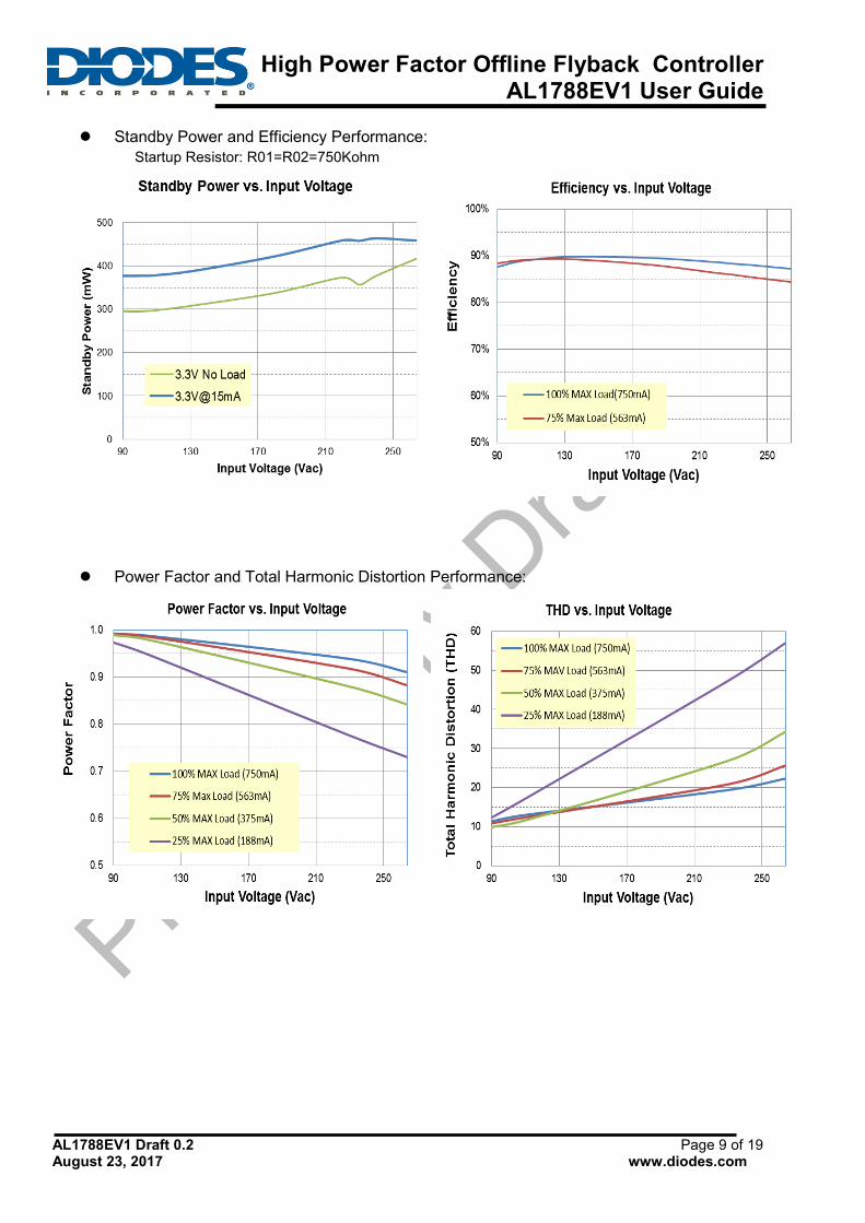
Standby Power and Efficiency Performance:
Startup Resistor: R01=R02=750Kohm
Power Factor and Total Harmonic Distortion Performance:

High Power Factor Offline Flyback Controller AL1788EV1 User Guide
AL1788EV1 Draft 0.2 Page 10 of 19 August 23, 2017 www.diodes.com
UVLO, Startup Time and Standby Power :
UVLO-ON and UVLO-OFF R01=R02=750K, Startup time=562ms
CH1:VCC CH2:Vgate CH1:VCC CH2:VO1 CH3:3.3V CH4:VH
R01=R02=375K, Startup time=318ms R01=R02=545K, Startup time=408ms
CH1:VCC CH2:VO1 CH3:3.3V CH4:VH CH1:VCC CH2:VO1 CH3:3.3V CH4:VH
Startup Time and Standby Power vs. Startup Resistor
Startup Resistor 1500Kom 1090Kohm 750Kohm
Startup Time 562ms 408ms 318ms
Standby Power 390.2mW 417.5mW 471.6mW
Note:
Low startup resistors reduce the startup time, but will increase standby power.
High Power Factor Offline Flyback Controller AL1788EV1 User Guide
AL1788EV1 Draft 0.2 Page 11 of 19 August 23, 2017 www.diodes.com
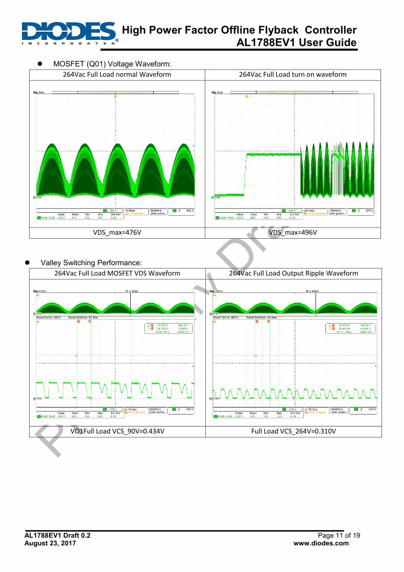
MOSFET (Q01) Voltage Waveform:
264Vac Full Load normal Waveform 264Vac Full Load turn on waveform
VDS_max=476V VDS_max=496V
Valley Switching Performance:
264Vac Full Load MOSFET VDS Waveform 264Vac Full Load Output Ripple Waveform
VO1Full Load VCS_90V=0.434V Full Load VCS_264V=0.310V

High Power Factor Offline Flyback Controller AL1788EV1 User Guide
AL1788EV1 Draft 0.2 Page 12 of 19 August 23, 2017 www.diodes.com
Output Rectifier Diode (D31) Voltage Waveform:
264Vac Full Load normal Waveform 264Vac Full Load turn on waveform
VDF_max=428V VDF_max=516V
Current Sense Voltage Waveform:
90Vac Full Load normal Waveform 264Vac Full Load normal Waveform
Full Load VCS_90V=0.434V Full Load VCS_264V=0.310V

High Power Factor Offline Flyback Controller AL1788EV1 User Guide
AL1788EV1 Draft 0.2 Page 13 of 19 August 23, 2017 www.diodes.com
Over Current Protection:
110Vac; OCP current: 1.2A 230Vac; OCP current: 1.5A
CH1:VDS CH4:IO CH1:VDS CH4:IO
Short Circuit Protection:
110Vac; Output Short and Auto Recover 230Vac; Output Short and Auto Recover
CH1:VDS CH4:IO CH1:VDS CH4:IO

High Power Factor Offline Flyback Controller AL1788EV1 User Guide
AL1788EV1 Draft 0.2 Page 14 of 19 August 23, 2017 www.diodes.com
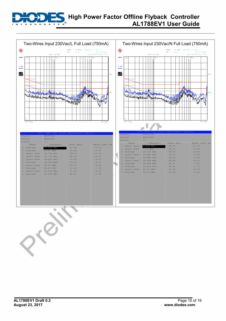
Conducted EMI Test:
Load Condition: VO1 add 54ohm Resistor (750mA).
Two-Wires Input 110Vac/L Full Load (750mA) Two-Wires Input 110Vac/N Full Load (750mA)
150 kHz 30 MHz
dBµV
dBµV
1 PK
MAXH
2 AV
MAXHTDS
6DB
RBW 9 kHz
MT 1 s
Att 10 dB
1 MHz 10 MHz
0
10
20
30
40
50
60
70
80
90
100
1
Marker 1 [T1 ]
40.55 dBµV
458.000000000 kHz
EN55022Q
EN55022A
Date: 23.JUN.2017 16:02:54
EDIT PEAK LIST (Final Measurement Results)
Trace1: EN55022Q
Trace2: EN55022A
Trace3: ---
TRACE FREQUENCY LEVEL dBµV DELTA LIMIT dB
1 Quasi Peak 29.69 MHz 50.79 -9.20
2 Average 29.758 MHz 41.24 -8.75
2 Average 29.802 MHz 40.90 -9.09
1 Quasi Peak 29.83 MHz 51.69 -8.30
2 Average 29.878 MHz 42.04 -7.95
1 Quasi Peak 29.922 MHz 51.72 -8.27
1 Quasi Peak 29.938 MHz 51.84 -8.15
2 Average 29.938 MHz 41.95 -8.04
1 Quasi Peak 29.962 MHz 51.99 -8.00
2 Average 29.962 MHz 41.87 -8.12
Date: 23.JUN.2017 16:02:28
150 kHz 30 MHz
dBµV
dBµV
1 PK
MAXH
2 AV
MAXHTDS
6DB
RBW 9 kHz
MT 1 s
Att 10 dB
1 MHz 10 MHz
0
10
20
30
40
50
60
70
80
90
100
1
Marker 1 [T1 ]
40.41 dBµV
458.000000000 kHz
EN55022Q
EN55022A
Date: 23.JUN.2017 16:01:08
EDIT PEAK LIST (Final Measurement Results)
Trace1: EN55022Q
Trace2: EN55022A
Trace3: ---
TRACE FREQUENCY LEVEL dBµV DELTA LIMIT dB
1 Quasi Peak 29.702 MHz 50.37 -9.62
1 Quasi Peak 29.794 MHz 50.77 -9.22
1 Quasi Peak 29.814 MHz 50.76 -9.23
2 Average 29.814 MHz 40.61 -9.38
2 Average 29.862 MHz 40.66 -9.33
2 Average 29.926 MHz 40.55 -9.44
1 Quasi Peak 29.95 MHz 51.08 -8.91
2 Average 29.95 MHz 41.20 -8.79
2 Average 29.974 MHz 41.58 -8.41
1 Quasi Peak 29.998 MHz 51.71 -8.28
Date: 23.JUN.2017 16:00:37
High Power Factor Offline Flyback Controller AL1788EV1 User Guide
AL1788EV1 Draft 0.2 Page 15 of 19 August 23, 2017 www.diodes.com
Two-Wires Input 230Vac/L Full Load (750mA) Two-Wires Input 230Vac/N Full Load (750mA)
150 kHz 30 MHz
dBµV
dBµV
1 PK
MAXH
2 AV
MAXHTDS
6DB
RBW 9 kHz
MT 1 s
Att 10 dB
1 MHz 10 MHz
0
10
20
30
40
50
60
70
80
90
100
1
Marker 1 [T1 ]
42.13 dBµV
458.000000000 kHz
EN55022Q
EN55022A
Date: 23.JUN.2017 16:10:34EDIT PEAK LIST (Final Measurement Results)
Trace1: EN55022Q
Trace2: EN55022A
Trace3: ---
TRACE FREQUENCY LEVEL dBµV DELTA LIMIT dB
2 Average 29.606 MHz 41.80 -8.19
2 Average 29.67 MHz 41.40 -8.59
1 Quasi Peak 29.738 MHz 49.24 -10.75
1 Quasi Peak 29.762 MHz 49.34 -10.65
1 Quasi Peak 29.882 MHz 51.40 -8.59
2 Average 29.906 MHz 43.38 -6.61
1 Quasi Peak 29.95 MHz 51.57 -8.42
2 Average 29.95 MHz 42.93 -7.06
1 Quasi Peak 29.966 MHz 51.55 -8.44
2 Average 29.974 MHz 42.53 -7.46
Date: 23.JUN.2017 16:10:14
150 kHz 30 MHz
dBµV
dBµV
1 PK
MAXH
2 AV
MAXHTDS
6DB
RBW 9 kHz
MT 1 s
Att 10 dB
1 MHz 10 MHz
0
10
20
30
40
50
60
70
80
90
100
1
Marker 1 [T1 ]
40.36 dBµV
458.000000000 kHz
EN55022Q
EN55022A
Date: 23.JUN.2017 16:08:55
EDIT PEAK LIST (Final Measurement Results)
Trace1: EN55022Q
Trace2: EN55022A
Trace3: ---
TRACE FREQUENCY LEVEL dBµV DELTA LIMIT dB
1 Quasi Peak 6.878 MHz 48.37 -11.63
1 Quasi Peak 7.13 MHz 50.10 -9.89
2 Average 29.762 MHz 40.04 -9.95
1 Quasi Peak 29.886 MHz 50.75 -9.24
2 Average 29.886 MHz 42.59 -7.40
1 Quasi Peak 29.906 MHz 50.82 -9.17
2 Average 29.906 MHz 42.77 -7.22
2 Average 29.926 MHz 42.85 -7.15
1 Quasi Peak 29.93 MHz 50.94 -9.05
2 Average 29.95 MHz 42.58 -7.41
Date: 23.JUN.2017 16:08:20
High Power Factor Offline Flyback Controller AL1788EV1 User Guide
AL1788EV1 Draft 0.2 Page 16 of 19 August 23, 2017 www.diodes.com
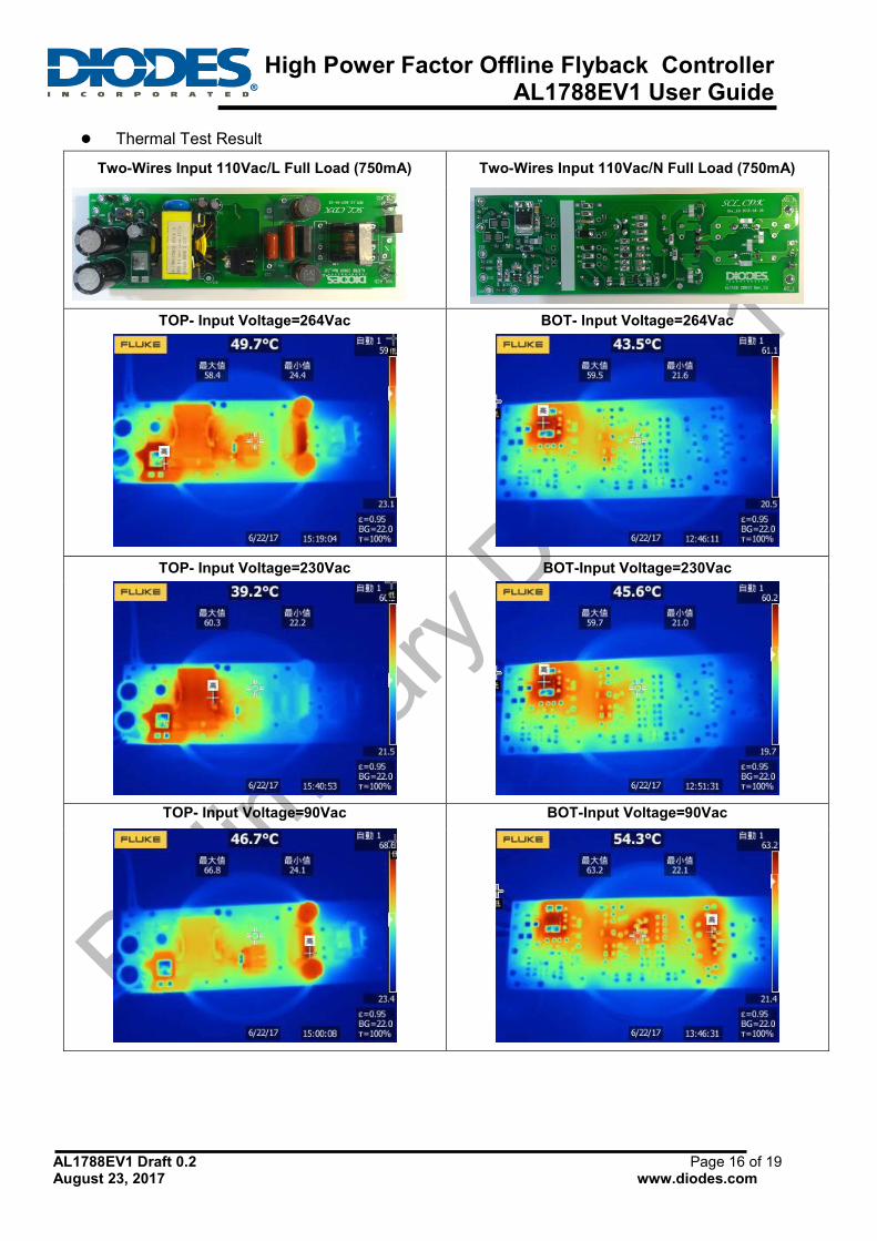
Thermal Test Result
Two-Wires Input 110Vac/L Full Load (750mA) Two-Wires Input 110Vac/N Full Load (750mA)
TOP- Input Voltage=264Vac BOT- Input Voltage=264Vac
TOP- Input Voltage=230Vac BOT-Input Voltage=230Vac
TOP- Input Voltage=90Vac BOT-Input Voltage=90Vac

High Power Factor Offline Flyback Controller AL1788EV1 User Guide
AL1788EV1 Draft 0.2 Page 17 of 19 August 23, 2017 www.diodes.com
Input / Output Application Description:
AL1788-CDK01 Application Description
Input Pin Functions:
Connector PIN# Name Function Description
VIN_ACL 1 VIN_ACL Connect to AC (L) Input
VIN_ACN 1 VIN_ACN Connect to AC (N) Input
Output Pin Functions:
Connector PIN# Name Function Description
VO1 1 VO1 42V Output for CV 750mA_max output
CN1 1 VO1 42V Output for CV
2 GND GND
GND1 1 GND GND
VO2 1 VO2 7.5V Output for CV 150mA_max output
CN2 1 VO2 7.5V Output for CV 150mA_max output
2 GND GND
GND2 1 GND GND
3V3 1 3V3 3.3V Output for MCU 200mA_Max output
CN3 1 3V3 3.3V Output for MCU 200mA_Max output
2 GND GND
GND3 1 GND GND
CN1
CN2
VIN_ACN
VIN_ACL
VIN_ACN CN1
CN2
CN3 VIN_ACL
CN2

High Power Factor Offline Flyback Controller AL1788EV1 User Guide
AL1788EV1 Draft 0.2 Page 18 of 19 August 23, 2017 www.diodes.com
Quick Start Guide
The evaluation board is preset at 42V (VO1) and 3.3V (3V3) for universal voltage input 100V < Vac < 240V
Ensure that the AC source is switched OFF or disconnected.
Connect the AC line wires of power supply to “L and N” on the board.
Turn on the AC main switch.
Measure CVout to check VO1 and 3V3 to ensure proper output voltages (42V and 3.3V)
Use Case examples for smart light bulb development
AL1788DCK01 + AL1794EV1 (30V DC-to-CC Linear CCR)
AL1788CDK01 + AL8860EV1 (40V DC-to-CC Switching Buck)
Reference web site:
AL1794EV1 - http://www.diodes.com/_files/evbd/AL1794EV1UserGuide.pdf
AL8860EV1 - http://www.diodes.com/_files/evbd/AL8860EV1UserGuide.pdf

High Power Factor Offline Flyback Controller AL1788EV1 User Guide
AL1788EV1 Draft 0.2 Page 19 of 19 August 23, 2017 www.diodes.com
IMPORTANT NOTICE DIODES INCORPORATED MAKES NO WARRANTY OF ANY KIND, EXPRESS OR IMPLIED, WITH REGARDS TO THIS DOCUMENT, INCLUDING, BUT NOT LIMITED TO, THE IMPLIED WARRANTIES OF MERCHANTABILITY AND FITNESS FOR A PARTICULAR PURPOSE (AND THEIR EQUIVALENTS UNDER THE LAWS OF ANY JURISDICTION). Diodes Incorporated and its subsidiaries reserve the right to make modifications, enhancements, improvements, corrections or other changes without further notice to this document and any product described herein. Diodes Incorporated does not assume any liability arising out of the application or use of this document or any product described herein; neither does Diodes Incorporated convey any license under its patent or trademark rights, nor the rights of others. Any Customer or user of this document or products described herein in such applications shall assume all risks of such use and will agree to hold Diodes Incorporated and all the companies whose products are represented on Diodes Incorporated website, harmless against all damages. Diodes Incorporated does not warrant or accept any liability whatsoever in respect of any products purchased through unauthorized sales channel. Should Customers purchase or use Diodes Incorporated products for any unintended or unauthorized application, Customers shall indemnify and hold Diodes Incorporated and its representatives harmless against all claims, damages, expenses, and attorney fees arising out of, directly or indirectly, any claim of personal injury or death associated with such unintended or unauthorized application. Products described herein may be covered by one or more United States, international or foreign patents pending. Product names and markings noted herein may also be covered by one or more United States, international or foreign trademarks. This document is written in English but may be translated into multiple languages for reference. Only the English version of this document is the final and determinative format released by Diodes Incorporated. LIFE SUPPORT
Diodes Incorporated products are specifically not authorized for use as critical components in life support devices or systems without the express written approval of the Chief Executive Officer of Diodes Incorporated. As used herein: A. Life support devices or systems are devices or systems which: 1. are intended to implant into the body, or 2. support or sustain life and whose failure to perform when properly used in accordance with instructions for use provided in the labeling can be reasonably expected to result in significant injury to the user. B. A critical component is any component in a life support device or system whose failure to perform can be reasonably expected to cause the failure of the life support device or to affect its safety or effectiveness. Customers represent that they have all necessary expertise in the safety and regulatory ramifications of their life support devices or systems, and acknowledge and agree that they are solely responsible for all legal, regulatory and safety-related requirements concerning their products and any use of Diodes Incorporated products in such safety-critical, life support devices or systems, notwithstanding any devices- or systems-related information or support that may be provided by Diodes Incorporated. Further, Customers must fully indemnify Diodes Incorporated and its representatives against any damages arising out of the use of Diodes Incorporated products in such safety-critical, life support devices or systems. Copyright © 2016, Diodes Incorporated www.diodes.com