ma16841 controller ic for dimmable offline led … · ma16841 controller ic for dimmable offline...
TRANSCRIPT

MAX16841
Controller IC for Dimmable Offline LED Lamps
19-6028; Rev 1; 6/13
Ordering Information appears at end of data sheet.
For related parts and recommended products to use with this part, refer to www.maximintegrated.com/MAX16841.related.
Typical Operating Circuits appear at end of data sheet.
EVALUATION KIT AVAILABLE
General Description
The MAX16841 is an LED driver for AC line (100V, 120V, 220V, and 230V AC) input lamps. It features proprietary control of the input current that allows lamps to dim smoothly from full to zero light intensity, while providing active power factor correction (PFC). It is a very flexible product that can be used in isolated (e.g., flyback) and nonisolated (e.g., buck) configurations. The conventional use of an optocoupler in isolated configurations can be avoided in MAX16841-based designs.
The constant frequency-control technique of the device allows maximization of the conversion efficien-cy at both low and high AC line by operating at the conduction mode that minimizes total conduction and switching losses.
The device can be configured for universal input (90V to 264V AC) dimmable applications, allowing the design of an LED lamp that can be operated and dimmed worldwide.
This device can be used without electrolytic capacitors, thus maximizing the lamp lifetime. In this case, the LED current is a rectified sinusoid with a frequency that is twice the AC line frequency.
The device also features thermal shutdown, current limit, open LED protection, and VCC undervoltage lockout. The MAX16841 is available in an 8-pin SO package and operates over the -40NC to +125NC temperature range.
Applications
Retrofit LED Lamps with Triac Dimming
Universal Input LED Retrofit Lamps
Industrial and Commercial Lighting
Residential LED Lighting
Features
S Smooth Dimming with Leading-Edge (Triac) and Trailing-Edge Dimmers
S Active Power Factor Correction
S Nonisolated (e.g., Buck) and Isolated (e.g., Flyback) Topologies
S Universal 90V to 264V AC Input Range
S Constant Frequency-Control Scheme Maximizes Efficiency at High and Low AC Line Voltage
S Constant Power Control with No Need for Optocouplers
S Very-Low Quiescent Current
S Output Open and Short Protection
S Thermal Shutdown
S Available in an 8-Pin SO Package
For pricing, delivery, and ordering information, please contact Maxim Direct at 1-888-629-4642, or visit Maxim Integrated’s website at www.maximintegrated.com.
MAX16841
Controller IC for Dimmable Offline LED Lamps
2Maxim Integrated
IN to GND ..............................................................-0.3V to +26VNDRV, DIMOUT to GND ........................... -0.3V to (VIN + 0.3V)All Other Pins to GND .............................................-0.3V to +6VNDRV Continuous Current ..............................................Q10mADIMOUT Continuous Current ............................................Q2mAContinuous Power Dissipation (TA = +70NC)
8 SO (derate 7mW/NC above +70NC) ..................588.2mW
Operating Temperature Range ........................ -40NC to +125NCJunction Temperature .....................................................+150NCStorage Temperature Range ............................ -65NC to +150NCLead Temperature (soldering, 10s) ................................+300NCSoldering Temperature (reflow) ......................................+260NC
8 SO Junction-to-Ambient Thermal Resistance (BJA) (based on S8+2) ...........................136NC/W
Junction-to-Case Thermal Resistance (BJC) (based on S8+2) .............................38NC/W
ABSOLUTE MAXIMUM RATINGS
Note 1: Package thermal resistances were obtained using the method described in JEDEC specification JESD51-7, using a four-layer board. For detailed information on package thermal considerations, refer to www.maximintegrated.com/thermal-tutorial.
Stresses beyond those listed under “Absolute Maximum Ratings” may cause permanent damage to the device. These are stress ratings only, and functional opera-tion of the device at these or any other conditions beyond those indicated in the operational sections of the specifications is not implied. Exposure to absolute maximum rating conditions for extended periods may affect device reliability.
PACKAGE THERMAL CHARACTERISTICS (Note 1)
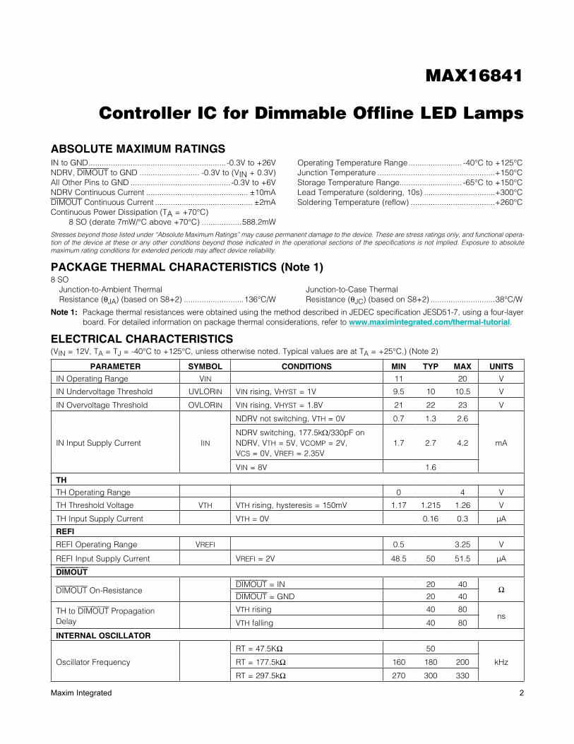
ELECTRICAL CHARACTERISTICS(VIN = 12V, TA = TJ = -40NC to +125NC, unless otherwise noted. Typical values are at TA = +25NC.) (Note 2)
PARAMETER SYMBOL CONDITIONS MIN TYP MAX UNITS
IN Operating Range VIN 11 20 V
IN Undervoltage Threshold UVLORIN VIN rising, VHYST = 1V 9.5 10 10.5 V
IN Overvoltage Threshold OVLORIN VIN rising, VHYST = 1.8V 21 22 23 V
IN Input Supply Current IIN
NDRV not switching, VTH = 0V 0.7 1.3 2.6
mANDRV switching, 177.5kW/330pF on NDRV, VTH = 5V, VCOMP = 2V, VCS = 0V, VREFI = 2.35V
1.7 2.7 4.2
VIN = 8V 1.6
TH
TH Operating Range 0 4 V
TH Threshold Voltage VTH VTH rising, hysteresis = 150mV 1.17 1.215 1.26 V
TH Input Supply Current VTH = 0V 0.16 0.3 FA
REFI
REFI Operating Range VREFI 0.5 3.25 V
REFI Input Supply Current VREFI = 2V 48.5 50 51.5 FA
DIMOUT
DIMOUT On-ResistanceDIMOUT = IN 20 40
IDIMOUT = GND 20 40
TH to DIMOUT Propagation Delay
VTH rising 40 80ns
VTH falling 40 80
INTERNAL OSCILLATOR
Oscillator Frequency
RT = 47.5KI 50
kHzRT = 177.5kI 160 180 200
RT = 297.5kI 270 300 330
MAX16841
Controller IC for Dimmable Offline LED Lamps
3Maxim Integrated
Note 2: All parameters are tested at TA = +25NC only. Limits over temperature are guaranteed by design.
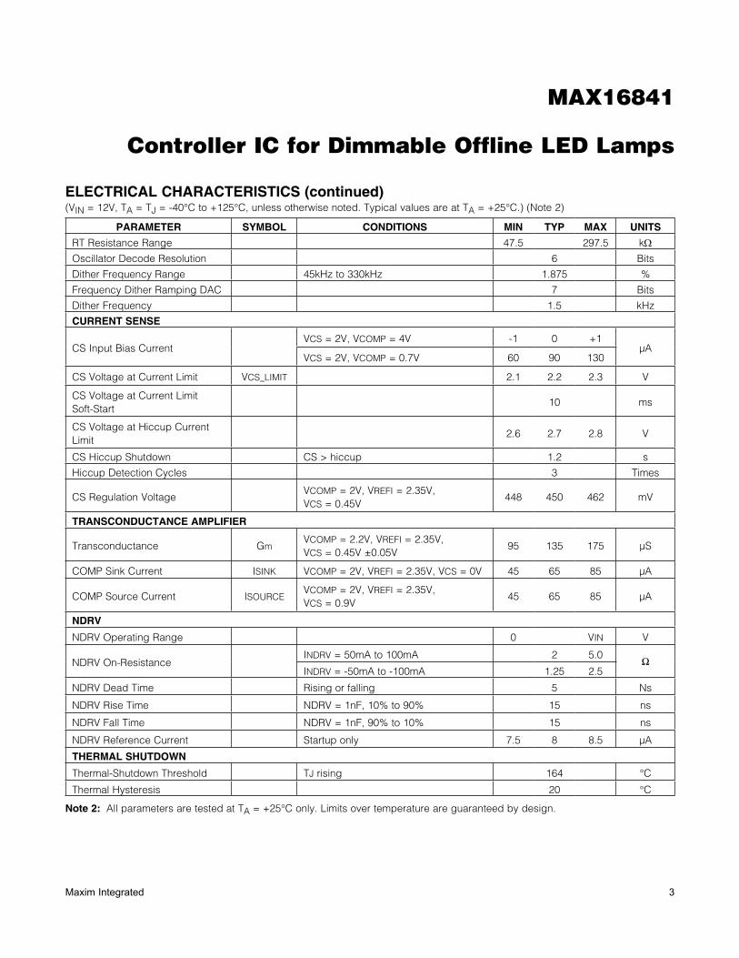
ELECTRICAL CHARACTERISTICS (continued)(VIN = 12V, TA = TJ = -40NC to +125NC, unless otherwise noted. Typical values are at TA = +25NC.) (Note 2)
PARAMETER SYMBOL CONDITIONS MIN TYP MAX UNITS
RT Resistance Range 47.5 297.5 kWOscillator Decode Resolution 6 Bits
Dither Frequency Range 45kHz to 330kHz 1.875 %
Frequency Dither Ramping DAC 7 Bits
Dither Frequency 1.5 kHz
CURRENT SENSE
CS Input Bias CurrentVCS = 2V, VCOMP = 4V -1 0 +1
FAVCS = 2V, VCOMP = 0.7V 60 90 130
CS Voltage at Current Limit VCS_LIMIT 2.1 2.2 2.3 V
CS Voltage at Current Limit Soft-Start
10 ms
CS Voltage at Hiccup Current Limit
2.6 2.7 2.8 V
CS Hiccup Shutdown CS > hiccup 1.2 s
Hiccup Detection Cycles 3 Times
CS Regulation VoltageVCOMP = 2V, VREFI = 2.35V, VCS = 0.45V
448 450 462 mV
TRANSCONDUCTANCE AMPLIFIER
Transconductance GmVCOMP = 2.2V, VREFI = 2.35V, VCS = 0.45V Q0.05V
95 135 175 FS
COMP Sink Current ISINK VCOMP = 2V, VREFI = 2.35V, VCS = 0V 45 65 85 FA
COMP Source Current ISOURCEVCOMP = 2V, VREFI = 2.35V, VCS = 0.9V
45 65 85 FA
NDRV
NDRV Operating Range 0 VIN V
NDRV On-ResistanceINDRV = 50mA to 100mA 2 5.0
IINDRV = -50mA to -100mA 1.25 2.5
NDRV Dead Time Rising or falling 5 Ns
NDRV Rise Time NDRV = 1nF, 10% to 90% 15 ns
NDRV Fall Time NDRV = 1nF, 90% to 10% 15 ns
NDRV Reference Current Startup only 7.5 8 8.5 FA
THERMAL SHUTDOWN
Thermal-Shutdown Threshold TJ rising 164 NC
Thermal Hysteresis 20 NC
MAX16841
Controller IC for Dimmable Offline LED Lamps
4Maxim Integrated
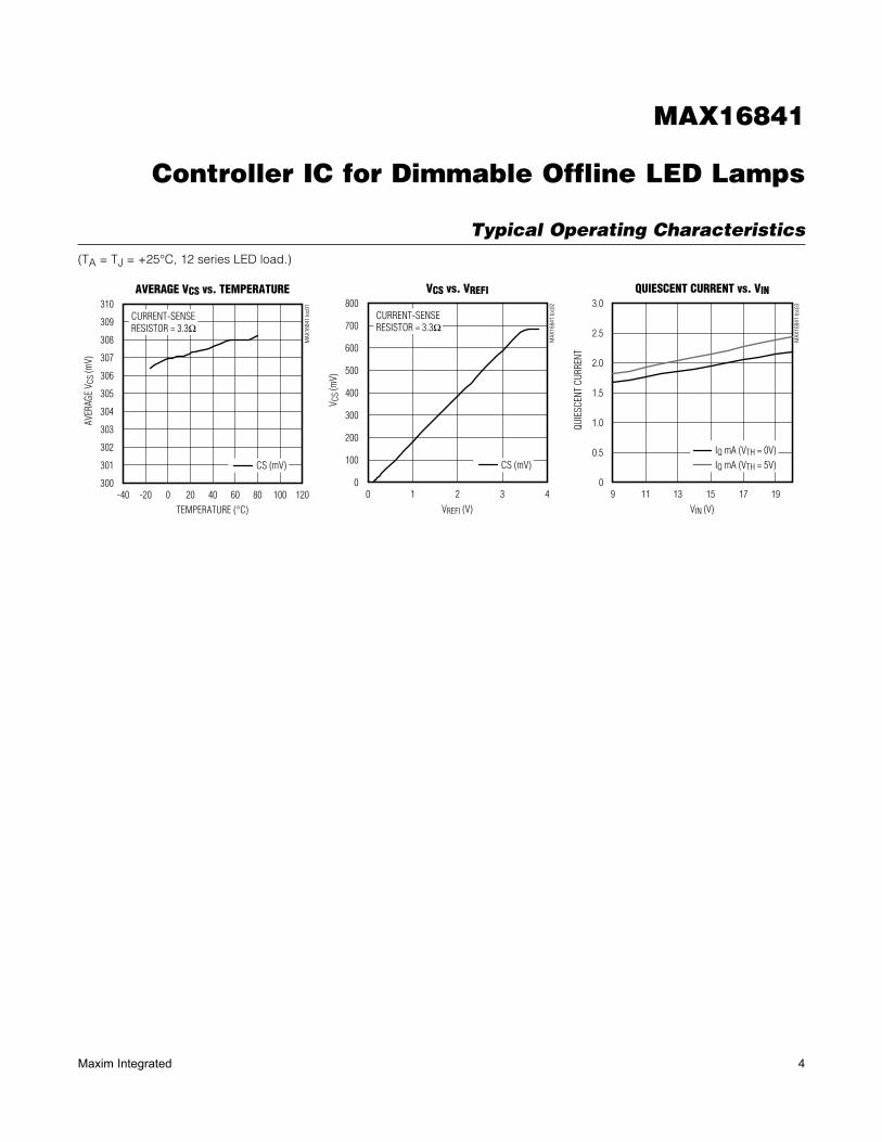
Typical Operating Characteristics(TA = TJ = +25NC, 12 series LED load.)
AVERAGE VCS vs. TEMPERATUREM
AX16
841
toc0
1
TEMPERATURE (°C)
AVER
AGE
V CS
(mV)
1008040 600 20-20
301
302
303
304
305
306
307
308
309
310
300-40 120
CS (mV)
CURRENT-SENSE RESISTOR = 3.3I
VCS vs. VREFI
MAX
1684
1 to
c02
VREFI (V)
V CS
(mV)
321
100
200
300
400
500
600
700
800
00 4
CS (mV)
CURRENT-SENSE RESISTOR = 3.3I
QUIESCENT CURRENT vs. VIN
MAX
1684
1 to
c03
VIN (V)
QUIE
SCEN
T CU
RREN
T
1917151311
0.5
1.0
1.5
2.0
2.5
3.0
09
IQ mA (VTH = 5V)
IQ mA (VTH = 0V)
MAX16841
Controller IC for Dimmable Offline LED Lamps
5Maxim Integrated
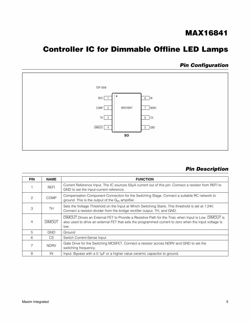
Pin Description
Pin Configuration
PIN NAME FUNCTION
1 REFICurrent Reference Input. The IC sources 50FA current out of this pin. Connect a resistor from REFI to GND to set the input-current reference.
2 COMPCompensation Component Connection for the Switching Stage. Connect a suitable RC network to ground. This is the output of the Gm amplifier.
3 THSets the Voltage Threshold on the Input at Which Switching Starts. This threshold is set at 1.24V. Connect a resistor-divider from the bridge rectifier output, TH, and GND.
4 DIMOUTDIMOUT Drives an External FET to Provide a Resistive Path for the Triac when Input is Low. DIMOUT is also used to drive an external FET that sets the programmed current to zero when the input voltage is low.
5 GND Ground
6 CS Switch Current-Sense Input
7 NDRVGate Drive for the Switching MOSFET. Connect a resistor across NDRV and GND to set the switching frequency.
8 IN Input. Bypass with a 0.1FF or a higher value ceramic capacitor to ground.
REFI+
COMP
TH
1
2
3
4
8
7
6
5DIMOUT
IN
NDRV
CS
GND
SO
TOP VIEW
MAX16841
MAX16841
Controller IC for Dimmable Offline LED Lamps
6Maxim Integrated
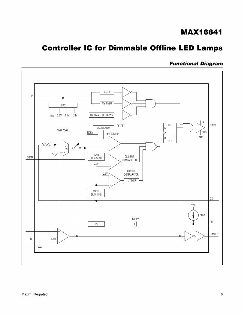
Functional Diagram
MAX16841
10msSOFT-START
OSCILLATOR
THERMAL SHUTDOWN
2.2V
2.7V
1.24V
CS LIMITCOMPARATOR
2.4VP-PNDRV
HICCUPCOMPARATOR
200nsBLANKING
100mV
1s TIMER
1/5
S Q
R QCLR
SET
GND
IN
VIN UVLO
VIN OV
BIAS
IN
COMP
TH
GND
DIMOUT
REFI
CS
NDRV
Gm
VCC 2.2V 2.3V 1.24V
50µA
VCC
MAX16841
Controller IC for Dimmable Offline LED Lamps
7Maxim Integrated
Detailed Description
The MAX16841 is a fixed-frequency offline LED driver IC that is compatible with both leading-edge triac dim-mers and trailing-edge transistor dimmers. The device uses a fixed-frequency average current-mode control scheme to control the switching current in the MOSFET. In addition, a peak-limit comparator is used to limit the peak switching current during overload and transient conditions. The peak-limit comparator has a threshold of 2.2V. For the active PFC, the device uses a proprietary current-control scheme where the averaged switch cur-rent on a cycle-by-cycle basis is set to a programmed DC value. This maximizes the efficiency of the converter by operating in continuous-conduction mode (CCM) at low AC line voltage (100V to 120V) and in discontinuous-conduction mode (DCM) at high AC line voltage (220V to 240V). Switching is initiated when the voltage on the TH pin exceeds a threshold of 1.24V. In the case of the buck configuration, the VTH falling threshold should be set in such a way so that the input voltage exceeds the maximum forward voltage of the LED string. In the case of the buck-boost or flyback configuration, this threshold can be set lower.
The device also uses a proprietary current-sense scheme to regulate the LED current.
The device switching frequency is adjustable from 50kHz to 300kHz using a single resistor from NDRV to ground. The device operates over a wide 11V to 20V supply voltage. The device’s switching MOSFET gate driver sources and sinks up to 1A, making it capable of driving high-voltage MOSFETs in offline LED driver applica-tions for power ranges up to 25W. The device allows for dimming with leading-edge and trailing-edge dimmers.
Additional features include thermal shutdown and overvoltage protection.
INThe device is powered up by the voltage at IN. All the internal regulators derive power from IN. The operational voltage is between 11V and 20V.
THTH sets the threshold for switching. Switching is initiated once TH crosses 1.24V. The TH comparator has a 150mV hysteresis. In a buck configuration, the VTH falling thresh-old should be set in such a way so that the input voltage exceeds the maximum forward voltage of the LED string. In a buck-boost configuration, the VTH falling threshold can be set to a lower level.
DIMOUTFor proper operation with triac dimmers, the load con-nected to the dimmer should draw at least the startup current when the dimmer is in the off state. For proper operation of the timing circuit of the dimmer, there should always be a close-current path. To ensure this, a bleeder resistor is connected across IN and GND with the help of an external FET. DIMOUT drives this external FET on when VTH goes below the falling threshold. The bleeder resistor is disconnected when VTH crosses its rising threshold, resulting in better performance and efficiency.
Internal OscillatorThe internal oscillator of the device is programmable from 50kHz to 300kHz. Connect a single resistor from NDRV to GND to set the oscillator frequency. Upon power-up, an 8FA of current sinks into this resistor. An internal ramp is then compared against the voltage on NDRV to determine the oscillator frequency.
Frequency DitheringThe device incorporates a frequency-dithering feature. This feature helps to reduce EMI.
n-Channel MOSFET Switch Driver (NDRV)The NDRV driver drives the gate of an external n-channel switching MOSFET. NDRV switches between IN and GND. NDRV is capable of sourcing/sinking 1A of peak current, allowing the device to switch MOSFETs in an offline LED driver application. The average current drawn from the supply to drive the external MOSFET depends on the MOSFET gate charge and switching frequency. Use the following equation to calculate the MOSFET driver supply current:
NDRV G SWI Q f= ×
Switching MOSFET Current Sense (CS)The switching MOSFET current-sense resistor should be connected to the CS pin of the device. The device con-trols the average of the CS signal to a level determined by the REFI voltage. Internal leading-edge blanking of 200ns (typ) is provided to avoid premature turn-off of the switching MOSFET in each switching cycle. A peak-limit comparator is used to limit the peak switch current during overload and transient conditions. The peak-limit comparator has a threshold of 2.2V (typ).
MAX16841
Controller IC for Dimmable Offline LED Lamps
8Maxim Integrated
Input-Current Setting (REFI)REFI is the external reference for programming the input current of the LED driver. The input current is proportinal to the REFI voltage. The IC sources 50FA current out of this pin and the voltage at the REFI pin can also be set by connecting a resistor from REFI to GND. Internally, the REFI signal is downshifted by 100mV and then attenua-ted by a factor of 5. The attenuated signal is applied to the positive terminal of the internal error amplifier and this signal sets the reference for the controller.
Error-Amplifier Output (COMP)The device includes an internal transconductance current error amplifier with a typical Gm of 150FS. The output of the error amplifier is controlled by the TH comparator output. When the TH comparator is high, the output of the error amplifier connects to COMP. When the TH comparator is low, the error amplifier is disconnected from COMP, preserving the charge on the compensation capacitor. COMP is connected to the positive terminal of the PWM comparator.
The device incorporates an average current-mode control scheme to regulate the input current. The control loop regulates the average of the CS signal to a level determined by the REFI voltage. The control loop consists of the current-sense resistor (RCS) connected across CS and GND, the transconductance current error amplifier, an oscillator providing a 2.4V ramp at switching frequency, the control voltage on the positive input of the Gm amplifier, and the PWM comparator.
Overvoltage-Protection Input (OVP)This is the protection feature in a flyback converter during an open LED condition. The IN pin is connected to the auxiliary winding of the flyback transformer. During an open LED condition, the IN voltage increases and NDRV is disabled once the IN voltage reaches 22.5V (typ). When the IN voltage drops by 2V, NDRV is enabled.
Short-Circuit ProtectionDuring an output short condition, the inductor current keeps increasing with input voltage as there is no nega-tive voltage across the inductor during the off period of the switching cycle. During this condition, the CS voltage signal peak is at a higher level because the inductor current is at a higher level than during the normal condi-tion. Once the CS signal exceeds the hiccup threshold of 2.7V (typ), the internal hiccup block gets activated. Switching is disabled for 1s (typ) if CS exceeds 2.7V (typ) for three times.
Thermal ProtectionThe device enters into thermal-shutdown mode when junction temperature exceeds +160NC. During thermal shutdown, NDRV is disabled. The device recovers from thermal-shutdown mode once the junction temperature drops by 20NC.
Applications Information
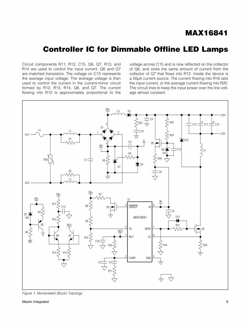
Figure 1 shows a MAX16841-based, triac-dimmable, PFC, nonisolated-buck offline LED driver. Components L1, L2, L3, and C1 provide EMI filtering. During the turn-on instant of triac dimming, there would be significant ringing due to high inrush current to charge the input capacitor (C9). The ringing could cause the line current to fall to zero and this would turn off the triac. R3, R22, and C14 act as a damper and help to limit the inrush current and ringing. Due to R3, the efficiency of the sup-ply decreases. The damper circuit can be omitted in nondimming applications. The circuit, consisting of D4, R5, C2, D3, R6, R4, and Q5, bypasses R3 with Q1 after 1ms of dimming instant, thereby reducing the power dissipation in R3 and improving efficiency. During the turn-on instant, capacitor C2 is charged by a constant-current source formed by D3, R6, R4, and Q5. Within 1ms time, sufficient voltage develops across C2 to fire the SCR Q1. Diode D4 provides fast discharge of C2. Resistors R8, R9, and R10 program the switching thresh-old. The rising threshold should be set at a voltage higher than the maximum LED string voltage. When the input voltage is below the falling threshold, DIMOUT drives the Q3 FET on, connecting R7 across the diode-bridge positive and GND. Thus, a close circuit is formed for the timing circuit of the triac. Diode D2 blocks capacitors C9 and C14 to discharge through R7. This helps to reduce the inrush current during the triac turn-on instant.
The circuit consisting of R23, R24, D6, and Q2 is a linear regulator and provides bias to the device.
The buck-converter circuit is formed by C9, LED+, LED-, C10, L5, Q4, D10, D11, and R20. Capacitor C9 provides a path for the switching frequency currents. Maximum value of this capacitor is limited by the input power-factor requirements. The higher the value of C9, the lower the input power factor.
Since the input-voltage waveform to the buck converter is a rectified sinusoid at line frequency, the LED current has a ripple at double-line frequency. Electrolytic capacitors C11 and C12 filter this double-line frequency ripple.
MAX16841
Controller IC for Dimmable Offline LED Lamps
9Maxim Integrated
Circuit components R11, R12, C15, Q6, Q7, R13, and R14 are used to control the input current. Q6 and Q7 are matched transistors. The voltage on C15 represents the average input voltage. The average voltage is then used to control the current in the current-mirror circuit formed by R12, R13, R14, Q6, and Q7. The current flowing into R12 is approximately proportional to the
voltage across C15 and is now reflected on the collector of Q6, and sinks the same amount of current from the collector of Q7 that flows into R12. Inside the device is a 50FA current source. The current flowing into R16 sets the input current, or the average current flowing into R20. The circuit tries to keep the input power over the line volt-age almost constant.
Figure 1. Nonisolated (Buck) Topology
Q2
D6
D10
15V
D318V
Q3
F1 L1
L3
D1
D2
1
3
DB+
4
2
R1
R2
AC2
AC1
LED+
LED-
R3
R5
R22 R23
R24
R34
C14
C13 L5
C10 C11 C12
C8
C9
D4Q1
L2
R26 C1
C2
R20R18
R17
R16
R10
R13
R12
R6
R4
R11
R14
Q7Q6
Q5R9
R7
R8 DIMOUT
TH
REFI
COMP GND
CS
NDRV
IN
IN8
7
6
52
1REFI
REFI3
4
U1
Q4
C5
C4C3
C16
D12
R21
MAX16841
DB+DB+
DB+
DB-
G
C15
G
DB-
MAX16841
Controller IC for Dimmable Offline LED Lamps
10Maxim Integrated
Resistors R16 and R20The average current in resistor R16 is the average input current of the buck converter.
If POUT is the output power, then the input power is given by:
OUTIN
ININ
M
M INrms
IN
CSCS
P
LP IN Lmax
PP
PI
2 V
V 2 V
I R20 0.1VR16
10µAV 80%
RIL
I I 0.5 I
=η× π
=×
= ×
× +=
×=
= + × ∆
ILP is the switch peak current. Maximum peak in the switch current occurs at the peak level of the highest input voltage.
VCS is 2.2V. Allow 80% margin for tolerances.
Inductor SelectionFor optimum efficiency, inductor L5 must be operated in continuous-conduction mode.
The current in the inductor would be at its maximum level at peak of the highest input voltage. LED string voltage is assumed constant. Calculate the duty cycle at peak of the highest input voltage.
LED
INmax
VD
2 V=
×
The percentage peak-to-peak ripple is considered between 30% and 60% of the inductor current. Assuming 60% peak-to-peak inductor current ripple, the maximum inductor current is given by:
OUTLmax
LED
PI
2 V× π
=×
The minimum value of the inductor is given by:
( )INmax LED
Lmax SW
2 V V DLmin
0.6 I f
× − ×=
× ×
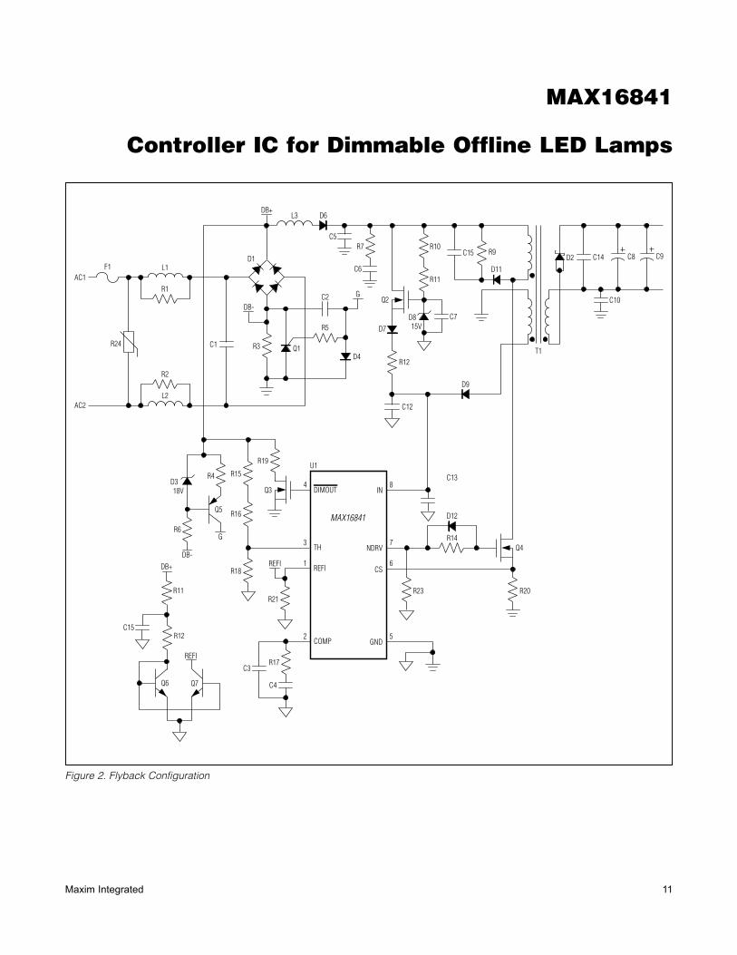
Figure 2 shows a PFC triac, dimmable, isolated (flyback topology) offline LED driver.
Here the current through the Q4 MOSFET is controlled. Current through Q4 is the same as the input current of the flyback converter. The input-side circuitry is the same as in the nonisolated buck LED driver that was previously described. During startup, the device is powered up from Q2, R10, R11, and D8. Bootstrap from the bias winding on the transformer turns off the Q2 MOSFET, thus saving power from high-voltage line. Here the switching threshold programmed by R15, R16, and R18 can be lower than the LED string voltage.
Output-side electrolytic capacitors C8 and C9 are used for filtering the double-line frequency current ripple in LED current.
During an open LED condition, the voltage across the output capacitors increases and is reflected on the bias-winding side.
Once the bias-winding voltage goes above 22.5V (typ), NDRV is disabled and the Q4 MOSFET turns off.
Choose the transformer turns ratio based on the voltage rating of the MOSFET. Use the following expression to calculate primary-secondary turns ratio:
DSmax INmaxPS
LEDmax
0.8 V VN
V× −
=
where:
NPS is the primary-secondary turns ratio
VDSmax is the voltage rating of the Q4 MOSFET
VINmax is the maximum peak input voltage
VLEDmax is the maximum voltage of the LED string
Factor 0.8 is taken into account for the voltage spikes, due to transformer-leakage inductance.
Use the following equation to calculate bias-secondary turns ratio:
ASLEDmax
18VN
V=
where NAS is the bias-secondary turns ratio and 18V is the bias voltage for the device.
MAX16841
Controller IC for Dimmable Offline LED Lamps
11Maxim Integrated
Figure 2. Flyback Configuration
Q2
D8
D2
D11
15V
D318V Q3
F1 L1
L3
D1
D6
DB-
R1
R2
AC2
AC1
R3
R5
R7 R10R9
R11
R12
C6
C15
C10
C7
C14 C8 C9
C12
C5
D4
D7
Q1
L2
R24 C1
C2 G
R20R23
R17
R21
R18
R6
Q5R16
R15R4
R19
TH
REFI
COMP GND
CS
NDRV
IN
U1
Q4
C13
C4
C3
D12
R14
DIMOUT
MAX16841
DB-
G
REFI
REFI
D9
T1
4
3
1
2
8
7
6
5
DB+
Q6 Q7
DB+
R12C15
R11
MAX16841
Controller IC for Dimmable Offline LED Lamps
12Maxim Integrated
Choose the transformer’s magnetizing inductance (Lm) in such a way so that the transformer operates in DCM above 120V AC input. DCM operation at higher voltages reduces switching losses in the Q4 MOSFET. Use the fol-lowing equation to calculate Lm:
2
IN SW
ININ
170V DLm
I f 2
PI
340V
×=
× ×
× π=
where D is the switching duty cycle at 170V DC and fSW is the switching frequency.
In DCM conditions, the peak current in Lm can be calculated with the help of the following equation:
IN INmaxP
SW
2 I VI
Lm f× ×
=×
where VINmax is the maximum peak input voltage.
Feedback CompensationLoop Compensation for
Nonisolated Buck (R17, C3, C4)The switching converter small-signal transfer function contains a pole at origin and a zero. The zero location is inversely related to inductor current and inductance value. The minimum frequency of the zero location is:
LEDZmin
Lmax
Vf
2 L I=
× π× ×
Design the loop compensation in such a way so that the loop crossover is near fZmin. Place the compensation zero formed by R17 and C4 at fZmin/5. R20 is given by:
Lmax
m P P
Zmin
I R20R17
G V
5C4
2 f R17
−
×=
×
=× π × ×
where Gm is the transconductance of the internal error amplifier and VP-P is 2.4V.
Place the compensation pole formed by R17 and C3 at 5 x fZmin:
Zmin
1C3
2 5 f R17=
× π× × ×
Loop Compensation for Flyback Driver (R17, C3, C4)
The switching converter small-signal transfer function is identical to the buck transfer function. The zero location is inversely related to primary-magnetizing inductance and its current. The minimum frequency of the zero location is:
LED PZmin
Lmax S
V Nf
2 Lm I N= ×
× π× ×
Design the loop compensation in such a way so that the loop crossover is near fZmin. Place the compensation zero formed by R17 and C4 at fZmin/5. R20 is given by:
Lmmax
m P P
Zmin
I R20R17
G V
5C4
2 f R17
−
×=
×
=× π × ×
where Lm is the magnetizing inductance of the flyback transformer, Gm is the transconductance of the internal error amplifier, and VP-P is 2.4V.
Place the compensation pole formed by R17 and C3 at 5 x fZmin:
Zmin
1C3
2 5 f R17=
× π× × ×
MAX16841
Controller IC for Dimmable Offline LED Lamps
13Maxim Integrated
Layout RecommendationsCareful PCB layout is critical to achieve low switching losses, and clean, stable operation. The switching- converter portion of the circuit has nodes with very fast voltage changes that could lead to undesirable effects on the sensitive parts of the circuit.
Follow the guidelines below to reduce noise as much as possible:
1) Ensure that all heat-dissipating components have adequate cooling.
2) Isolate the power components and high-current paths from the sensitive analog circuitry.
3) Have a power ground plane for the switching- converter power circuit under the power compo-nents (input filter capacitor, output filter capacitor, inductor, MOSFET, rectifier diode, and current-sense resistor). Connect GND to the power ground plane as close as possible to GND. Connect all other ground
connections to the power ground plane using vias close to the terminals
4) There are two loops in the power circuit that carry high-frequency switching currents. One loop is when the MOSFET is on (from the input filter capacitor posi-tive terminal, through the output capacitor, inductor, switching MOSFET, and current-sense resistor, to the input capacitor negative terminal). The other loop is when the MOSFET is off (from the output capacitor negative terminal, through the inductor, the rectifier diode, and output filter capacitor positive terminal). Analyze these two loops and make the loop areas as small as possible. Wherever possible, have a return path on the power ground plane for the switching currents on the top-layer copper traces or through power components. This reduces the loop area con-siderably and provides a low-inductance path for the switching currents. Reducing the loop area also reduces radiation during switching.
MAX16841
Controller IC for Dimmable Offline LED Lamps
14Maxim Integrated
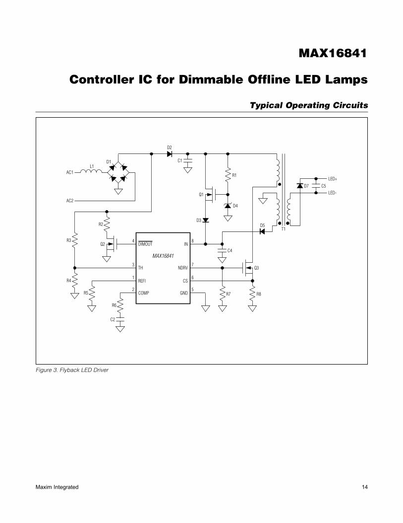
Figure 3. Flyback LED Driver
Typical Operating Circuits
L1AC1
D2
C1
Q1
Q2
R1
D4
D5
D7
R8R7
R6
R5
R4
TH
REFI
COMP GND
CS
NDRV
IN4
3
1
2
8
7
6
5
R3
R2
Q3
T1
LED+
LED-
C5
C4
C2
D3
AC2
D1
MAX16841
DIMOUT
MAX16841
Controller IC for Dimmable Offline LED Lamps
15Maxim Integrated
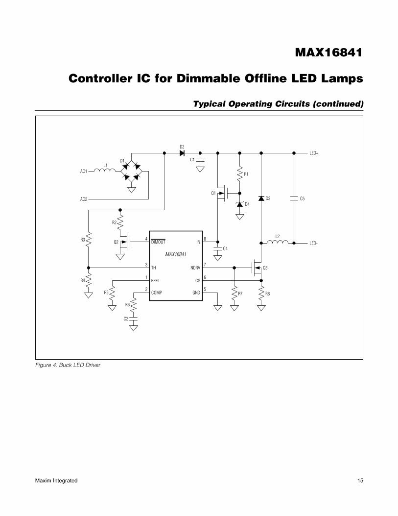
Figure 4. Buck LED Driver
Typical Operating Circuits (continued)
TH
REFI
COMP GND
CS
NDRV
IN4
3
1
2
8
7
6
5
MAX16841
DIMOUT
L1
L2
AC1
D2
C1
Q1
Q2
R1
D4D3
R8R7
R6
R5
R4
R3
R2
Q3
LED+
LED-
C5
C4
C2
AC2
D1

MAX16841
Controller IC for Dimmable Offline LED Lamps
16Maxim Integrated
Figure 5. Buck-Boost LED Driver
Typical Operating Circuits (continued)
L1
D3
AC1
D2
C1
Q1
Q2
R1
D4L2
R8R7
R6
R5
R4
R3
R2
Q3
LED-
LED+
C5
C4
C2
AC2
D1
TH
REFI
COMP GND
CS
NDRV
IN4
3
1
2
8
7
6
5
MAX16841
DIMOUT

MAX16841
Controller IC for Dimmable Offline LED Lamps
17Maxim Integrated
Ordering Information
+Denotes a lead(Pb)-free/RoHS-compliant package.
Chip Information
PROCESS: BiCMOS
Package Information
For the latest package outline information and land patterns (foot-prints), go to www.maximintegrated.com/packages. Note that a “+”, “#”, or “-” in the package code indicates RoHS status only. Package drawings may show a different suffix character, but the drawing pertains to the package regardless of RoHS status.
PART TEMP. RANGE PIN-PACKAGE
MAX16841ASA+ -40NC to +125NC 8 SO
PACKAGE TYPE
PACKAGE CODE
OUTLINE NO.
LAND PATTERN NO.
8 SO S8+2 21-0041 90-0096
MAX16841
Controller IC for Dimmable Offline LED Lamps
Maxim Integrated cannot assume responsibility for use of any circuitry other than circuitry entirely embodied in a Maxim Integrated product. No circuit patent licenses are implied. Maxim Integrated reserves the right to change the circuitry and specifications without notice at any time. The parametric values (min and max limits) shown in the Electrical Characteristics table are guaranteed. Other parametric values quoted in this data sheet are provided for guidance.
Maxim Integrated 160 Rio Robles, San Jose, CA 95134 USA 1-408-601-1000 18© 2013 Maxim Integrated Products, Inc. Maxim Integrated and the Maxim Integrated logo are trademarks of Maxim Integrated Products, Inc.
Revision History
REVISIONNUMBER
REVISIONDATE
DESCRIPTIONPAGES
CHANGED
0 10/11 Initial release —
1 6/13 Corrected CS regulation voltage unit in Electrical Characteristics table 3