high performance mo n electrode fabricated by … · n electrode fabricated by solution precursor...
TRANSCRIPT

High Performance MoxN Electrode Fabricated by Solution
Precursor Plasma Spraying
by
Yakov Gazman
A thesis submitted in conformity with the requirements
for the degree of Master of Applied Science
Department of Materials Science and Engineering
University of Toronto
© Copyright by Yakov Gazman 2015

ii
High Performance MoxN Electrode Fabricated by Solution
Precursor Plasma Spraying
Yakov Gazman
Master of Applied Science
Department of Materials Science and Engineering
2015
Abstract
Changing climate and decreasing availability of fossil fuels stimulate the use of alternative
energy sources and energy storage devices such as electrochemical capacitors The current study
investigates the implementation of SPPS (Solution Precursor Plasma Spraying) for the deposition
of high surface area electrochemical capacitor electrodes. A high performance MoxN
electrochemical capacitor electrode was produced by solution precursor plasma spraying for the
first time. The best electrode exhibited an initial capacitance of 62.4 mF cm-2
at a scan rate of
100 mV sec-1
. The capacitance decreased by 22% after the first 1000 cycles, but the performance
then stabilized, decreasing by only 0.15% over cycles 4000 to 5000 and exhibiting a capacitance
of 30mF cm-2
after 5000 cycles. SPPS is a novel deposition method, thus further understanding
and optimization of the process is required to improve the performance and manufacturability,
but a clear potential was proven.

iii
Acknowledgments
I would like to express my sincere gratitude to my supervisor, Professor Thomas W. Coyle, for
his continuous support and encouragement throughout my M.A.Sc. thesis research. I would like
to extend my appreciation to Professor Keryn Lian and her research group, especially Haoran
(George) Wu for his expert guidance and help with electrochemical testing. I also wish to
acknowledge the contributions of Sal Boccia, Abdolkarim Danaei, Dr. Larry Pershin, and Dr.
Stan Lugowski. Finally, I wish to thank my family for their endless love and support towards my
education.

iv
Table of Contents
Acknowledgments ..................................................................................................................... iii
Table of Contents ...................................................................................................................... iv
List of Tables ........................................................................................................................... vii
List of Figures ......................................................................................................................... viii
Abbreviations ........................................................................................................................... xii
Chapter 1: Introduction ............................................................................................................... 1
1.1 Objective ........................................................................................................................ 4
Chapter 2: Literature review ....................................................................................................... 5
2 5
2.1 Electric double layer capacitance (EDLC) ....................................................................... 5
2.2 Pseudocapacitance .......................................................................................................... 7
2.3 Surface area and pore network ........................................................................................ 8
2.4 Transition metal materials ............................................................................................. 10
2.4.1 Molybdenum oxide and nitride .......................................................................... 11
2.4.2 Topotactic transformation .................................................................................. 14
2.5 Molybdenum deposition techniques .............................................................................. 17
2.6 Solution precursor plasma spraying ............................................................................... 18
2.6.1 Plasma plume structure ...................................................................................... 18
2.6.2 Plasma forming gases ........................................................................................ 20
2.6.3 Powder injected ................................................................................................. 21
2.6.4 Liquid injected nano-structure coatings ............................................................. 22
2.6.5 Effect of liquid injection and standoff ................................................................ 26

v
2.7 Previous results ............................................................................................................. 27
Chapter 3: Experimental Procedure .......................................................................................... 29
3 29
3.1 Substrate preparation .................................................................................................... 29
3.2 Solution preparation ...................................................................................................... 29
3.3 Molybdenum oxide electrode fabrication ...................................................................... 30
3.4 Oxide to nitride transformation ..................................................................................... 32
Chapter 4: Characterization Techniques .................................................................................... 33
4 33
4.1 X-ray diffraction (XRD) ............................................................................................... 33
4.2 Scanning electron microscope (SEM) ........................................................................... 33
4.3 Energy dispersive spectroscopy (EDS) .......................................................................... 34
4.4 Glow discharge optical emission spectroscopy (GD-OES) ............................................ 34
4.5 Cyclic Voltammetry (CV) ............................................................................................. 35
Chapter 5: Results and Discussion ............................................................................................ 39
5 39
5.1 Study of coating thermal history ................................................................................... 39
5.1.1 Standoff distance effect ..................................................................................... 40
5.1.2 Solution flow rate effect .................................................................................... 42
5.1.3 GD-OES analysis .............................................................................................. 45
5.2 Molybdenum oxide/nitride on stainless steel ................................................................. 47
5.2.1 Molybdenum oxide ........................................................................................... 47
5.2.2 Molybdenum nitride .......................................................................................... 50
5.3 Molybdenum oxide/nitride on titanium ......................................................................... 52
5.3.1 Molybdenum oxide ........................................................................................... 52
5.3.2 Molybdenum nitride .......................................................................................... 56

vi
5.3.3 High cycle testing .............................................................................................. 60
5.4 Titanium electrode modification ................................................................................... 62
5.4.1 Substrate surface modification ........................................................................... 62
5.4.2 Coating thickness modification .......................................................................... 64
5.4.3 Converting gas modification .............................................................................. 65
Chapter 6: Conclusions and Future Work ................................................................................. 69
6 71
6.1 Future work .................................................................................................................. 71
References ................................................................................................................................ 73

vii
List of Tables
Table 1-1: Energy storage device comparison [2] ....................................................................... 2
Table 2-1: Comparison between EDLC and Pseudo capacitance [2] ........................................... 7
Table 2-2: Physical and electrochemical properties of the early transition metal nitrides and
carbides [37]. ............................................................................................................................ 12
Table 2-3: The effects of heating rate on the intermediate and final reaction products at a
constant NH3 flow rate of 7 L min−1
[49] .................................................................................. 17
Table 3-1: Unchanged and studied parameter during the thesis research ................................... 31
Table 3-2: Temperature program reaction used in nitridation process ....................................... 32

viii
List of Figures
Figure 1-1: Ragone plot for comparing energy storage devices [4] .............................................. 1
Figure 1-2: Characterization of electrochemical capacitors by their charge storage mechanism ... 3
Figure 2-1: Schematic illustration of a double layer capacitor [4] ................................................ 5
Figure 2-2: (a) Helmholtz layer (b) Diffuse layer (c) Helmholtz and diffuse combined [1] .......... 6
Figure 2-3: Normalized capacitance as a function of pore size [1] ............................................... 8
Figure 2-4: Partial stripping and de-solvating of electrolyte ion [21] ........................................... 9
Figure 2-5: Schematic of a double layer and importance of porosity [2] .................................... 10
Figure 2-6: Molybdenum/water system, potential as a function of PH [30] ............................... 11
Figure 2-7: Cycle voltammogram of molybdenum oxide in 5 x 10⁻³
M H2SO4, scan rate 50 mV s-l
[31] .......................................................................................................................................... 12
Figure 2-8: Phase diagrams of Mo-O and Mo-N [39] ................................................................ 13
Figure 2-9: CV profiles of molybdenum nitride film deposited by CVD [16] ............................ 14
Figure 2-10: Molybdate unit cell showing the layer-like arrangement of molybdenum (green) and
oxygen atoms (red) [46]............................................................................................................ 15
Figure 2-11:α-MoO3 transformation path into molybdenum nitride [3] .................................... 15
Figure 2-12:DTA/TGAstudyofα-MoO3 under flowing ammonia [3] ..................................... 16
Figure 2-13: Plasma formation and plume structure adapted from [4] ....................................... 19
Figure 2-14: SEM micrograph illustrating the effect of plasma tail temperature gradient on the
formation of different α-MoO3 morphologies [5] ...................................................................... 20
Figure 2-15: Thermal conductivity and enthalpy [58] ............................................................... 21

ix
Figure 2-16: Creation of coating by stacking molten splats [4] .................................................. 21
Figure 2-17: In-flight velocity of Al2O3 particlesofdiameters18,23,39and46μmsuspendedin
an Ar – H2 plasma forming gas mixture with a velocity of 600m sec-1
[59] ............................... 22
Figure 2-18: Suspension stream penetration and break-up under different injection pressures (a)
0.4MPa (b) 0.7MPa [6] ............................................................................................................. 24
Figure 2-19: Decomposition process of a solution droplet inside a plasma jet [5,7] ................... 25
Figure 2-20: Schematic representation of the SPPS setup [19] .................................................. 26
Figure 2-21: Cooling effect of standoff distance and water injection on DC-arc plasma [8] ...... 27
Figure 2-22: Normalized capacitance as a function of standoff distance found in Mehdi Golozar’s
research [5]............................................................................................................................... 28
Figure 3-1: Torch and sample setup: (a) torch with connecting gas, water and solution lines (b)
sample and sample holder placement ........................................................................................ 30
Figure 4-1: GD-OES depth profile analysis example ................................................................ 35
Figure 4-2: Cyclic voltammetry representation as a simple electronic circuit ............................ 36
Figure 4-3: Three electrode CV schematic for film testing [9] .................................................. 37
Figure 4-4: Ideal shapes of cyclic voltammograms for a reversible, diffusion-controlled reaction
(left), and thin-layer conditions for a reversible reaction in a thin film (right). [9] ..................... 38
Figure 5-1: Substrate temperature as a function of deposition time ........................................... 40
Figure 5-2: XRD patterns of samples deposited at 55mm and 75mm standoff distances ............ 41
Figure 5-3: As deposited samples at (a) 55mm (b) 65mm (c) 75mm standoff distance .............. 42
Figure 5-4: Substrate temperature as a function of deposition time for five different nozzles .... 43
Figure 5-5: Peak temperature as a function of nozzle diameter .................................................. 43

x
Figure 5-6: SEM micrographs of samples deposited with various nozzle diameters: (a)100μm,
(b)200μm, and (c)330μm ........................................................................................................ 44
Figure 5-7: GD-OES analysis of as deposited coating (55mm SD) ............................................ 45
Figure 5-8: GD-OES analysis of as deposited coating (75mm SD) ............................................ 46
Figure 5-9: Cycle voltammetry plots of as deposited samples deposited at 55, 60, and 65mm SD
and 5.3mm RD ......................................................................................................................... 48
Figure 5-10: Cyclic voltammetry of as deposited samples on stainless steel with different RD.. 49
Figure 5-11: As deposited coating on stainless steel substrate post CV ..................................... 49
Figure 5-12: Cyclic voltammetry testing on nitride samples deposited on stainless steel ........... 50
Figure 5-13: SEM micrograph of post nitridation coating on stainless steel, showing exposed
substrate ................................................................................................................................... 51
Figure 5-14: Post CV samples of nitrited coatings deposited on stainless steel at 55, 65 and
75mm SD ................................................................................................................................. 52
Figure 5-15: SEM micrographs of as deposited samples on Ti substrate ................................... 53
Figure 5-16: Cyclic voltammetry testing for as-deposited samples on Ti substrate .................... 54
Figure 5-17: CV plot for as deposited sample at 75mm SD after 4 and 104 cycles .................... 54
Figure 5-18: High magnification SEM micrograph of as deposited sample on Ti substrate ....... 55
Figure 5-19: Molybdenum oxide solution after 1hr at 700C heat treatment .............................. 56
Figure 5-20: SEM micrographs of nitrided samples deposited at 55mm and 75mm SD ............. 57
Figure 5-21: High magnification SEM micrographs of post nitridation sample deposited at 55mm
SD ............................................................................................................................................ 57
Figure 5-22: EDS analysis of sample deposited at 55mm SD (a) on island (b) between islands . 58

xi
Figure 5-23: XRD patterns of nitrided samples deposited on Ti substrate ................................. 59
Figure 5-24: Cyclic voltammetry of nitride electrode deposited on Ti substrate at 55, 65 and
75mm SD ................................................................................................................................. 60
Figure 5-25: High cycle CV plot of nitrided sample deposited on Ti substrate .......................... 61
Figure 5-26: Capacitance as a function of cycle number for sample deposited at 65mm SD ...... 62
Figure 5-27: Cyclic voltammetry of (a) Cleaned Ti substrate (b) Cleaned and nitrided Ti
substrate ................................................................................................................................... 63
Figure 5-28: Capacitance as a function of standoff distance for different surface modifications 64
Figure 5-29: Cyclic voltammetry of 3 layer deposition ............................................................. 65
Figure 5-30: Low resolution SEM image of sample deposited at 75mm SD and heat treated in N2
................................................................................................................................................. 66
Figure 5-31: High resolution SEM micrographs of samples heat treated in N2 ......................... 66
Figure 5-32: XRD pattern of sample deposited at 55mm SD and heat treated in N2................... 67
Figure 5-33: EDS analysis of sample heat treated in N2 ............................................................ 68
Figure 5-34: Cyclic voltammetry plot of samples heat treated in N2 .......................................... 68
Figure 6-1: Schematic flow chart for better capacitance performance for oxide and nitride
coatings .................................................................................................................................... 71

xii
Abbreviations
SPPS: solution precursor plasma spraying
EDLC: Electric double layer capacitance
GD-OES: Glow discharge optical emission spectroscopy
SD: Standoff distance
RD: Raster distance
CACT: Center for Advanced Coating Technologies
TRP: Temperature programmed reaction
SEM: Scanning electron microscope
BET: Brunauer Emmett Teller
CV: Cyclic voltammetry
TGA: Thermal gravimetric analysis
DTA: Differential Thermal Analysis
RIR: Relative intensity ration

1
Chapter 1: Introduction
The constant rise in the world energy consumption forces the scientific community to develop
alternative methods of energy production that can be sustainable and with lower environmental
foot print. Because the new energy systems rely on the sun, wind and other alternative sources,
the production can be limited by the location and process thus increasing the importance of
energy storage devices [1-3].
Figure 1-1 presents a common method for the comparison of energy storage devices called a
Ragone plot. In this plot the vertical axis, specific power, represents the amount of energy that
can be delivered in a given amount of time, and the horizontal axis, specific energy, represents
how long the energy can be delivered. Electrostatic capacitors have a large specific power,
delivering a large amount of power but discharging very quickly. On the other hand batteries can
deliver energy for a very long time but only at relatively low rates.
Figure 1-1: Ragone plot for comparing energy storage devices [4]
One of the leading families in the field of storage devices are the electrochemical capacitors
(EC), also known as supercapacitors or ultracapacitors [5], which store electrical charge via
surface phenomena and avoid the deterioration of the electrode that occurs in batteries [2].

2
Electrochemical capacitors occupy the biggest and widest region in the Ragone plot. Along with
good efficiency, they offer excellent reversibility (90-95% or higher), long cycle life (>105) [2],
and fast charge/discharge which enables them to fill the gap between high energy batteries and
high power solid state capacitors [1-4, 6].
Table 1-1: Energy storage device comparison [2]
Super capacitor electrodes that are based on nano-carbon structures [6-8] store energy via a
surface phenomenon called double layer capacitance (EDLC), characterized by a thin
polarization layer that separates the charge at the electrode-electrolyte interface [1,2,6,7].
In addition to double layer capacitance, transition metal oxides/nitrides such as VxN [9], MoxN
[10,11], TiN [12] and conductive polymers [13] can allow charge transfer between the
electrolyte and electrode inducing slow and reversible oxidation-reduction reaction on the
electrode surface, called pseudo capacitance, which significantly increases the overall
capacitance [1,2,4]. A hybrid electrode combines both surface phenomena using EDLC and
pseudo materials on the same electrode; one of these hybrids is a molybdenum carbon electrode
[14]. Adding various metals to molybdenum oxide electrodes can also have positive effects on
the electrochemical performance of the electrode [15]. As both double layer and pseudo
capacitance are surface phenomena, reducing the average grain size and increasing the porosity
will create a larger surface area that is most desirable and critical for a high performance
supercapacitor electrode [1, 4]. Unlike conductive polymers that have slow diffusion processes
that increase the resistance and lower the stability, transition metal oxides have high specific
power and low resistance which increases the interest in such electrodes for application in

3
electrochemical capacitors. The current benchmark transition metal is RuO2, but ruthenium is a
very expensive metal [9,11,16], thus other low cost alternatives such as MoO3 and MoxN are
being developed.
Figure 1-2: Characterization of electrochemical capacitors by their charge storage mechanisms
Although molybdenum nitride has a much larger capacitance then its oxide counterpart, direct
deposition is not possible in atmospheric conditions and a temperature programed reaction (TPR)
in a nitrogen environment is required to convert the as-deposited oxide coating into nitride.
Many methods for molybdenum oxide deposition exist such as CVD [16, 17], electro deposition
[11], and spray pyrolysis [10], but solution precursor plasma spraying (SPPS) offers a robust and
controllable process capable of depositing high surface area coatings in atmospheric conditions,
and that is compatible with a reel to reel process for mass production. Because traditional
thermal spray, specifically DC-arc plasma spraying, involves the injection of powder particles
into the high temperature, high velocity plasma plume, the microstructure of the coating is
limited by the large size powder [18].
By injecting the feedstock in the form of an atomized solution precursor into the plasma torch, it
is possible to create a nano-scale microstructure consisting of hollow and broken spheres and a
pore network that is ideal for electrochemical capacitors application [19].
Charge Storage
Mechanism
Double layer Capacitance
Carbon Based
Pseudo Capacitance
Transition Metal
Oxide/Nitride
Conductive Polymers
4
Previous work conducted in our research group has revealed that shorter standoff distances and
closer raster patterns increase the total heat to which deposits are exposed, resulting in more
complete decomposition of the precursor and a higher capacitance for the molybdenum oxide
electrode [19]. But only thick coatings were produced and all electrodes completely disintegrated
after only 10 cyclic voltammetry cycles.
SPPS is a novel and not yet fully understood deposition system with various parameters such as
substrate material, substrate finish, standoff distance, solution concentration and many more that
can affect the final microstructure and electrochemical performance.
1.1 Objective
The objective of this research thesis is to deposit a molybdenum oxide coating with good
substrate adhesion by solution precursor plasma spraying, followed by a nitriding heat treatment
to transform the coating to molybdenum nitride, and then to perform electrochemical analysis of
the electrode capacitance and stability. The electrochemical behaviour will be linked to the
process parameters controlling the deposition and nitriding stages by characterizing the
microstructure, chemical composition and phase content of the coatings at each stage.

5
Chapter 2: Literature review
2.1 Electric double layer capacitance (EDLC)
The charge storage mechanism in a double layer capacitor involves an electrostatic adsorption of
oppositely charged ions on the surface of the negative electrode. When a potential difference
between the electrodes is created, the opposite charges in the electrolyte are drawn to the
electrodes, and a charge separation at the electrode/electrolyte accrues forming a 5-10Å interface
layer known as a double layer. EDLC electrodes do not undergo redox reactions as part of the
electrostatic charge storage; therefore the major difference from batteries is no limitation of the
electrochemical kinetics through a polarization resistance and therefore better power
performance. The absence of faradic reactions also eliminates the swelling in the active material
that batteries show during charge/discharge cycles [1].
Figure 2-1: Schematic illustration of a double layer capacitor [4]

6
The double layer capacitance is described by (2-1), where εr is the dialectic constant of the
electrolyte, ε0 is the dielectric constant of vacuum, d is the effective thickness of the double
layer, A is the electrode surface area :
𝑪 =𝜺𝒓𝜺𝟎𝑨
𝒅 (2-1)
At first, it was assumed that the charge accumulation is only due to the charge separation at the
electrode/electrolyte interface (Helmholtz layer), however later studies by Gouy-Chapman and
Stern Geary proven that a second layer exists (diffuse layer) which is defined by the
concentration gradient of the ions from the interface layer to the bulk of the electrolyte, figure 2-
2. Presently a joint model is accepted combining both the Helmholtz layer and diffuse layer in
the same model (c). Graphitic carbon, such as carbide-derived, carbon fabrics, fibers, nanotubes
and many more are suitable for this application [20], due to high conductivity, electrochemical
stability and open porosity.
Figure 2-2: (a) Helmholtz layer (b) diffuse layer (c) Helmholtz and diffuse combined [1]
7
2.2 Pseudocapacitance
Pseudo capacitors utilize both double layer capacitance and pseudo capacitance, and can be
composed of either conductive polymers or oxides and nitrides of transition metals such as
manganese, vanadium, nickel, cobalt, ruthenium, tantalum, iridium, iron or molybdenum. Due to
the multiple oxidation and coordination states of transition metals, the electrostatically adsorbed
ions on the electrode can undergo a reversible redox reaction with the electrode thus increasing
the overall capacitance [1].
Table 2-1: Comparison between EDLC and Pseudo capacitance [2]
The specific pseudo-capacitance exceeds that of carbon materials using double layer charge
storage, justifying the interest in these systems. But because the charge storage mechanism
involves redox reactions, like batteries, they often suffer from a lack of stability during cycling.
Capacitance of more than 600 F g-1
[1] has been reported for ruthenium oxide, which has been the
focus of research over the past 30 years. However, Ru-based aqueous electrochemical capacitors
are expensive, and the 1V voltage window limits their applications in small electronics. Other
transition metal oxides with various oxidation degrees, such as molybdenum oxides, are now
being explored as active materials for pseudo-capacitors.

8
2.3 Surface area and pore network
Initial research on the dependence of capacitance on pore volume and size, showed that the
capacitance increase was limited. Even for the most porous samples there was no linear
relationship between the capacitance and pore size, suggesting that pores smaller than 0.5 nm
were not accessible to hydrated ions.
Figure 2-3: Normalized capacitance as a function of pore size [1]
The peak in capacitance shifted to smaller pores for smaller ions. This behavior cannot be
explained by purely electrostatic reasons because all pores were either the same size or smaller
than a single ion, thus confirming that ions must be at least partially stripped of solvent
molecules in order to occupy the carbon pores in the EDLC structure. A combination of various
sizes that can accommodate all ions present in the electrolyte is a key feature in improving the
capacitance of ECs.

9
Figure 2-4: partial stripping and de-solvating of electrolyte ion [21]
Nanomaterials have improved the performance of Li-ion batteries, therefore the effect of nano-
structuringEC’sisanimportantresearchpossibility.Becausepseudo-capacitors store charge in
the first few nanometers from the surface, decreasing the particle size increases active material
usage by increasing the specific surface area. The charging mechanism of a thin electrically
conducting surface layer of oxide or oxy-nitride includes a combination of an electric double
layer and a faradic reaction at the surface of the nanoparticles. The high specific surface area and
interfacial exchange improvement of nano-sized particles was shown to improve the specific
capacitance and cycling stability for transition metal nitrides or oxides. The perfect candidate for
an electrochemical capacitor would be an active pseudo-capacitive electrode with large surface
area consisting of small grains/particles, highly porous, with a large pore size distribution and
open pore network [22].

10
Figure 2-5: Schematic of a double layer and importance of porosity [2]
2.4 Transition metal materials
A pseudo-capacitive material could be either a conductive polymer or a transition metal oxide or
nitride; conductive polymers have slower diffusive processes and a limited conductivity [13, 23].
Great interest is being shown in transition metal oxides/nitrides which have high conductivity
and low resistance, making them some of the best candidates for a pseudo-capacitive material.
Transition metal oxides and nitrides can include a variety of material such as VxN [9], TiN [12]
and MnO2 [24], but the most promising candidate in this family is ruthenium oxide. RuO2 is a
benchmark material in the transition metal family due to its long cycle life, high conductivity,
high specific capacitance and excellent reversibility showing capacitance as high as 1340F g-1
for
its hydrous from [25,26]. Although RuO2 is the perfect candidate in terms of electrochemical
performance, lack of abundance prevents the implementation of this material in a commercial,
mass production way [2]. This encourages research and development on alternative pseudo-
capacitive materials. One of this group of developing materials showing great potential is
crystallineα-MoO3 which has a large pseudo-capacitance and double layer capacitance [27].

11
Molybdenum nitride exhibits an even larger and more stable capacitive behavior which can be
processed via topo tactic transformation from the oxide without losing surface area.
2.4.1 Molybdenum oxide and nitride
Molybdenum has a very rich electrochemistry as a result of multiple coordination numbers and
oxidation states ranging from –II to +VI, as well as stability in natural and acidic environments
as shown in figure 2-6, resulting in the interest in molybdenum oxide and nitride coatings for
electrochemical applications such as capacitors and catalysts [28] [29].
Figure 2-6: Molybdenum/water system, potential as a function of pH [30]
A typical cyclic voltammetry diagram of molybdenum oxide (figure 2-7) in acidic electrolyte has
shown a partly double overlapping reduction and redox reaction due to molybdenum bronze
formation (AxMoO3 (0 < x< 2)) which is controlled by the diffusion of electrolyte ions into Mo
oxide [31] [32]. Electrochromism of such films is caused by the ion intercalation/deintercalation
reaction. Hydrogen ions were inserted into molybdenum oxide films to form hydrogen
molybdenum oxide bronzes, which can be formulated as [33, 34]:
𝑴𝒐𝑶𝟑 + 𝒙𝑯+ + 𝒙𝒆− ⟺ 𝑴𝒐𝑶𝟑−𝒙(𝑶𝑯)𝒙 (2-2)

12
Figure 2-7: Cycle voltammogram of molybdenum oxide in 5 x 10⁻³
M H2SO4, scan rate, 50 mV s-l [31]
Against Ag/AgCl at -0.5V molybdenum oxide electrodes show capacitive behavior, but the
asymmetrical anode and cathode current density and CV profile that has no mirror image causes
poor capacitive performance. Mo oxide is not the ideal pseudo capacitive material because at
potentials lower then -0.5V hydrogen evolution develops and at potentials higher than 1V the
passive layer is broken. In addition to significant separation between the cathodic and anodic
peaks, the electrode suffers from low electrical conductivity and poor reversibility [35, 36].
Table 2-2: Physical and electrochemical properties of the early transition metal nitrides and carbides [37].
Transformation of the oxide into nitride forms such as γ-Mo2N/δ-MoN/Mo3N2 [38] occurs
through a reduction mechanism and is strongly dependent on the converting gas and the thermal
profile applied during the process.

13
Figure 2-8: Phase diagrams of Mo-O and Mo-N [39]
Due to the low performance of the oxide form, the nitride form of molybdenum is usually
preferred. It has high conductivity, and excellent reversibility and pseudo-capacitive performance
[40, 41]. As shown in figure 2-9, the current vs potential curve (CV curve) is very rectangular,
symmetrical on the cathodic and anodic sides, with little resistance illustrated by the sharp peaks
at the edges of the scanned potential [42].Experimentsconductedontransformationofα-MoO3
into β phase molybdenum nitride revealed that small differences in impurity content and/or
crystallinity of the MoO3 can strongly influence the morphology and the content of molybdenum
nitride in the final product, illustrating the complexity and sensitivity of the process [43, 44].

14
Figure 2-9: CV profiles of molybdenum nitride film deposited by CVD [16]
2.4.2 Topotactic transformation
Asimpletransitionofα-MoO3 into γ-Mo2N/δ-MoN/Mo3N2 under flowing nitriding gas and high
temperature will result in grain and particle growth significantly lowering the active surface area.
Due to the fact that most deposition methods are not capable of depositing molybdenum nitride
coatings directly, a more effective transformation process which preserves the high surface area
is required. A very slow heating rate of 0.01K sec-1
between 417°C to 467°C in a N2-H2
atmosphere as part of a two stage process was shown by Volpe and Bourdattp to prevent
sinteringofα-MoO3 [45].

15
Figure 2-10: Molybdate unit cells showing the layer-like arrangement of molybdenum (green) and oxygen
atoms (red) [46]
Replacing oxygen with hydrogen in the octahedral planes without disruption of the orthorhombic
crystal (figure 2-10) structure resulted in formation of an oxygen deficient MoO2, while a higher
heating rate resulted in sintering of the molybdenum oxide particle. The second step was a faster
heating rate of 0.05K sec-1
from 467°C to 706°C resulting in transformation of MoO2 into Mo2N
while avoiding formation of molybdenum metal. This process, also known as TRP (temperature
reaction program), was utilized by Jaggers et al. by using NH3 gas in order to produce high
surface area molybdenum nitride powder. The reaction of molybdenum oxide under ammonia
has a more reductive activity path then in N2, involving a molybdenum oxy-nitride intermediate
phase shown in figure 2-11 [3, 10, 11].
Figure 2-11:α-MoO3 transformation path into molybdenum nitride [3]

16
The DTAplotsofα-MoO3 in figure 2-12 show no activity below a temperature of 375°C, but at
460, 595 and 695°C three endothermic peaks were observed. The first two peaks indicate the
formation of MoO2 and MoOxN1-x, which are intermediate phases in the transformation process.
The third peak corresponds to the transformation into nitride phases. Based on the TGA plot of
MoO2 under flowing NH3, no weight loss was observed until MoO2 reached 688°C and at 750°C,
the weight loss came to a halt and MoO2 transformed entirely into Mo2N with a trace of MoN. In
1993 Choi et al. described a temperature programmed reaction (TPR) for convertingα-MoO3 by
heating it under flowing NH3 gas in which the samples were rapidly heated from room
temperature up to 350°C, where the reaction with nitrogen started. Two heating stages followed
the preheat; the first from 350 to 450°C and the second from 450 to 700°C. The final step was a
1Hr dwell at 700°C [12].
Figure 2-12: DTA/TGA studyofα-MoO3 under flowing ammonia [3]
Further research conducted by Wise and Markel applied a similar approach, with a gas mixture
of 82% H2 and 18% N2 and a peak temperature of 660°C. They reported the creation of Mo
metal at 500°C and lower oxygen reducing activity thus lower transformation rate into
molybdenum nitride phases [13]. Heat treatment under pure N2 has a low oxygen reduction
potential and thus leads to a very limited transformation into intermediate phases of oxy-nitride
[3, 13, 14]. In 1997 Roberson, Finello and Davis reported a low oxygen concentration
molybdenum nitride electrode prepared using a two stage thermal profile under flowing

17
ammonia. The results in table 2-3 demonstrate that a high conversion rate can be achieved
without a dramatic effect on grain coarsening [49].
Table 2-3: The effects of heating rate on the intermediate and final reaction products at a constant NH3 flow
rate of 7 L min−1 [49]
2.5 Molybdenum deposition techniques
A substantial number of molybdenum oxide deposition methods are available, each with its
unique advantages and disadvantages, ranging from technical complications to industrial
considerations. For supercapacitor applications that are supposed to compliment or even replace
batteries in the field, the cost of the product is critical and often detrimental to the release of the
technology itself. Deposition methods such as vacuum evaporation [50], sputtering [51] and
chemical vapor deposition [17] require an expensive vacuum system that increases the cost for
an electrode, sol-gel deposition [52] requires multiple stages and solutions, complicating the
process and making development of a reel to reel process difficult. Electrodeposition [53] has
shown great promise in several literature papers due to a relative simple and cost effective
deposition process, but relatively low specific surface area is limiting the electrochemical
performance. Thermal processing of molybdenum solutions, such as spray pyrolysis [10] and
SPPS, have shown the best electrochemical performance due to large surface areas as well as
offering simple industrial application. Spray pyrolysis has small number of controllable

18
parameters thus limiting process control and preventing scale up. On the other hand solution
precursor plasma spraying is a simple process using only one solution in an atmospheric
environment, is compatible with a reel to reel application set-up, and a number of process
parameters offering the capability for process control. It is the method of choice in this thesis
work.
2.6 Solution precursor plasma spraying
SPPS is part of a large and well established coating deposition family called thermal spraying
which utilizes different thermal sources in order to melt/decompose a feedstock and accelerate it
toward a substrate, creating coatings for multiple applications. These include dense coatings for
wear and corrosion resistance, moderate porosity coatings such as thermal barrier coatings, and
high porosity coatings for applications such batteries and super capacitors. A subgroup of this
family is DC-arc plasma spraying in which an electric arc is created between a cathode and
anode inside a plasma torch, ionizing the flowing plasma forming gases. The feedstock in either
solid or liquid form is injected radially or axially into the plasma plume [54-56].
2.6.1 Plasma plume structure
In order to properly melt the particle feedstock and accelerate it toward the substrate to achieve
the desired final microstructure of the coating, many variables need to be sufficiently well
controlled. The final coating microstructure is determined by the velocity and temperature of the
particles impacting the surface, therefore the particles must spend sufficient time and distance
inside the plasma jet prior to the impact with the surface, in order to reach a temperature above
the melting temperature. The plasma plume exiting most DC torches is 4-6mm wide, with a
plasma velocity range of 600 – 2300m sec-1
. The short residence time inside the plasma jet is
often not sufficient to melt ceramic particles when using pure argon as the plasma forming gas,
and enhanced thermal mixtures are needed. Figure 2-13 shows a schematic DC arc torch
illustrating the different torch parts and the plasma plume. An electric arc is created between the

19
anode and cathode due to a very large electrical potential difference build up, this arc ionizes the
plasma forming gases that are forced through the torch opening.
Figure 2-13: Plasma formation and plume structure adapted from [4]
As the plasma expands outside of the torch different temperature zones are created, each zone
has an influence depending on the proximity to the core of the plume and the distance from the
torch. The effect of the temperature distribution on the coating microstructure of a molybdenum
oxide coating deposited by solution precursor spraying with a DC-arc plasma torch is shown in
Figure 2-14. As the distance from the torch increases, the lower the plasma temperature
becomes, resulting in smaller particles On the other hand if the distance is shorter the higher
temperature plasma core has a greater effect resulting in coarsening and particle growth. This
relative simple control of the standoff distance (SD) has a dramatic effect on the microstructure,
phase composition and eventually the overall electrochemical performance when applied in
energy storage devices [57].
e

20
Figure 2-14: SEM micrograph illustrating the effect of plasma tail temperature gradient on the formation of
different α-MoO3 morphologies [5]
2.6.2 Plasma forming gases
As well as plasma velocity and in-flight residence time, the thermal properties and composition
of the plasma forming gas and feedstock material are substantial factors in creating melted
particles or any other desirable form of surface coating. The forming gas is selected according to
its ability to transfer thermal energy to an in-flight particle during a short residence time.
Depending on the plasma source and the material feedstock, different mixtures of Ar, He, H2, N2,
O2, CH4 and CO2 are acceptable. A ternary gas mixture of Ar-He-H2 is one of the most common
gas mixtures used in the thermal coating industry. As argon alone has very low enthalpy and heat
transfer capabilities an additional gas is needed inside the plasma forming gas mixture [4]. The
short in flight time and high velocity of the plasma makes it difficult for particles to melt and
impinge on the substrate to form disk shaped lamellae coating structures. Likewise for liquid
feedstock the solvent has to evaporate, precipitates form, pyrolize and melt in-flight to have
splats. In order to introduce enough thermal energy and enthalpy to transform the feedstock in
flight, a high enthalpy and thermal conductivity plasma forming gas mixture is required. The

21
proposed solution was developed by the coating center at the University of Toronto which uses
gases such as CH4 and CO2 mixed with Ar, that together with a carbon cathode torch have better
thermal properties as shown in figure 2-15 [15, 58].
Figure 2-15: Thermal conductivity and enthalpy [58]
2.6.3 Powder feedstock
Conventional plasma spray techniques use powder material as the feedstock injected into the
high temperature zone of the plasma core to allow sufficient heating and subsequent melting of
particles prior to the substrate impact. The structure of such coatings is characterized by the final
morphology of each molten or semi-molten particle consecutively landing on the substrate
surface. These conventional micro-structured coatings are made up of many single splats formed
through a successive course of impacting, flattening, rapid cooling and solidification of an
individual molten or semi-molten particle [4, 59].
Figure 2-16: Creation of coating by stacking molten splats [4]
22
In order to create a sub-micron coating with high surface area and high porosity the powder size
has to be reduced. Although commercial nano-size powders are available, injecting them into the
core of the plasma jet by entraining them in a carrying gas as is done for larger particle size
powder requires a large carrying gas flow rate, which cools and disrupts the plasma plume. As
illustrated in figure 2-17 as the size of the powder is decreases the force needed for adequate
injection increases, requiring higher carrying gas velocity. For nano-size powder the velocity
required is in the same order of magnitude as the plasma jet itself, resulting in physical
disruption of the plasma jet and limitation of this process to a minimum of 5μm particles in
laboratory experiments [4, 60].
Figure 2-17: In-flight velocity of Al2O3 particlesofdiameters18,23,39and46μmsuspendedintheAr– H2
plasma forming gas with the velocity of 600m sec-1
[59]
2.6.4 Liquid feedstock and nano-structured coatings
SPPS uses precursor solutions as the feedstock injected into DC-arc plasma instead of the
powder used in conventional thermal spray processes to deposit nanocrystalline oxide coatings.

23
The deposits typically exhibit fine grain sizes, high porosity levels, and high surface area, which
are ideal for application as electrochemical electrodes in devices such as solid oxide fuel cells,
Li-ion batteries, super-capacitors, and sensors [61]. Studies have revealed fractured hollow
spheres to be the signature structure of these porous, high surface area coatings. The liquid
atomization while entering the plasma, such as primary breakup caused by the Rayleigh
instability and secondary break-up caused by the plasma velocity, has a significant effect of the
coating structure. Additional parameters of the solution and plasma process itself must be taken
into account. The gas Weber number represents the competitive effects of inertia and surface
tension forces, thus illustrating the likelihood of a droplet to undergo further breakup, is
expressed by equation 2-3:
Where ρg is the gas mass density, 𝑢𝑟 is the relative velocity between gas and liquid, 𝑑1 is the
droplet or liquidjet diameter, 𝜎1 is the surface tension of the liquid.
Plasma properties such as temperature and velocity affect the Weber number. In addtion the
method of liquid injection into the core of the plasma jet has a major effect on the break up
mechanism and droplet size [62, 63].
2.6.4.1 Gas atomization
Gas atomization is a method in which the injected liquid stream is broken up by a high velocity
gas stream. The breakup mechanism depends on liquid and gas velocity as described by the
Weber number. The mechanisms are classified as bag break-up (12<We<100) where the droplets
is stretched and swept in flow direction, stripping break-up (100<We>350) where thin sheets are
drawn from the deforming droplets, and catastrophic break-up (We>350) where a multi stage
effect is happening. The biggest disadvantage of the gas atomization method is the addition of a
complexity factor in the form of controlling the atomization gas that requires additional valves
and gas controlling features.

24
2.6.4.2 Mechanical atomization
Mechanical atomization has two systems associated with it. In the first a pressurized reservoir
feed liquid to a nozzle where a magnetostrictive rod superimposes pressure pulses at frequencies
up to a few tens of kHz. In pulse mechanical break-up the droplet diameter is a function of liquid
flow velocity therefore the droplet size and velocity cannot be controlled separately. In a second
system, which was utilized in this thesis work, the liquid from a pressurized tank is forced
though a nozzle with a given diameter 𝑑𝑖 and produces a liquied jet with velocity 𝜐1and a
diameter of about1.5 − 1.8𝑑𝑖. The liquid exits the nozzle and breaks up at a distance of 100 −
150𝑑𝑖 from the nozzle due to Rayleigh–Taylor instabilities. Because of the natural physical
break-up of the liquid it has less disruption effect on the plasma jet and is the preferred injection
method in many cases.
Figure 2-18: suspension stream penetration and break-up under different injection pressures (a) 0.4MPa (b)
0.7MPa [6]
In low concentration precursor solutions the evaporation of the solvent results in the solubility
limit being reached at the surface of the droplet, causing precipitation at the surface and thus
forming hollow spheres [64]. In contrast, high concentration solution result in a more uniform
composition and precipitation occurs throughout the bulk and surface of the droplets resulting in
solid particles and dense coatings, figure 2-19. Understanding and controlling the evolution of
theprecursorsolutiondropletsintheplasmajetiscrucialinproducingα-MoO3 deposits of fine
grain sizes, high porosity levels and high surface area.

25
Figure 2-19: Decomposition process of solution droplet inside a plasma jet [5,7]
The full system illustrated in figure 2-20 shows the different elements described above in a
complete system configuration. The plasma forming gases which are controlled by the torch
control console are being forced with high velocity into the torch chamber where a powerful arc
between the cathode and anode is ionizing the flowing gas creating a high temperature and
enthalpy plasma. Air is being used in order to pressurize a solution that is injected into the
plasma creating in flight material that is deposited on a substrate at different standoff distances.

26
Figure 2-20: Schematic representation of the SPPS setup [19]
2.6.5 Effect of liquid injection and standoff distance
In DC plasma torches used for spraying (power level of generally <50 kW), typical temperatures
are between 8000 and 14 000 K, depending on the plasma forming gases. The room temperature
liquid that is injected into the plasma has a cooling effect on the plasma jet; this cool down can
be as much as 3000K depending on the amount of liquid injected and the downstream location
where the temperature is measured (standoff distance). As illustrated in figure 2-21, without
injection of water the spectroscopy measurement shows a temperature drop of about 2000K as
the standoff distance increased from 5mm to 15mm. With water injection at a rate of 20 mL
min-1
the temperature was roughly 2000K lower at both distances [65].

27
Figure 2-21: Cooling effect of standoff distance and water injection on DC-arc plasma [8]
2.7 Previous results
This thesis work is based on research that was conducted in the CACT in 2012 by Mehdi
Golozar. This research work has proved the concept of molybdenum oxide electrode deposited
by SPPS. As shown in figure 2-22 the result achieved by this research where an capacitive
behavior of molybdenum oxide electrode on stainless steel substrates and a connection to the
thermal history of the coating, but the relative capacitance to other deposition methods and other
transition metal electrodes is very low and the stability of the electrode was shown to be very
problematic as the electrode disintegrated after only 10 cycle voltammetry cycles. A better
understanding of the thermal history of the coating, higher electrochemical performance and
better stability were the major objective of this research thesis [66].

28
Figure 2-22: Normalized capacitance as a function of standoff distance shown in Mehdi Golozar research [5]

29
Chapter 3: Experimental Procedure
3.1 Substrate preparation
Substrate preparation and modification was shown to increase coating adhesion thus increasing
the electrochemical performance of the electrode because this characteristic is strongly affected
by the structural integrity of the coating and electrode. One of the theories on coating adhesion of
thermal spraying process has shown that if the surface roughness is in the order of the splats that
are formed by the spaying process a maximum coating substrate adhesion can be achieved. The
solution droplets created during the primary and secondary breakdown are on the order of 20-
30μm, therefore in order to achieve maximum adhesion of the coating the roughness should of
the same order. Three types of surface modification were implemented in this thesis work aimed
to increase surface adhesion and control the created oxide phases. The first is polishing with 320
grit particle size of SiC which was implemented on all 75×12.5mm, 1mm thick stainless steel
(304) and titanium (Grade 2) samples, creating surface roughness in the order of the droplets
[67]. The two additional modifications were implemented on Ti substrates only as results of a
literature reference to increases coating adhesion and control of oxide phase after nitridation
process [10]. Following this guideline two sets of experiment were performed, the first consisted
of only cleaning the surface with Alcohol (Commercial Alcohols), Acetone ((CH3)2CO,
CALEDON) following by immersion in 0.1M Hydrochloric acid (HCl, J.T.Baker) at 90°C for 10
minutes in order to remove organics and surface oxides in order to increase surface adhesion The
third set was cleaned in the same way that the previous, but then also nitrided inside a tube
furnace at 700°C for 1Hr in ammonia gas (4.5 Grade, Praxair) flowing at 0.115 mL sec-1
.
3.2 Solution preparation
Solution properties have an effect on the coating porosity and process limitation due to
precipitation of molybdenum salt that clogs the injection nozzle during spraying. As a result only
one solution precursor variation was prepared by mixing 0.1 Kg of ammonium molybdate (para)
tetrahydrate ((NH4)6Mo7O24·4H2O, Alfa Aesar) with 900 mL of DI water and stirred with a
magnetic stirrer for 10 minutes to dissolve all the salt in the water.

30
3.3 Molybdenum oxide electrode fabrication
Fabrication of electrodes was performed in a monitored spray booth which houses an x,y,z axis
robot to which the torch was attached, with gas lines and water line for cooling. The prepared
substrates were placed in front of the torch on sample holders. The solution injection nozzle,
which was connected to a pressurized tank containing the 10% solution at 0.48MPa, was
attached under the plasma torch at the plume exit oriented to allow radial injection into the plume
(figure 3-1). Thermocouples connect to the back of the sample substrate, with temperatures
recorded through a Omega TC-08 data acquisition module in order to measure the temperature
developed on the substrate during spraying.
Figure 3-1: Torch and sample setup (a) torch with connecting gas, water and solution lines (b) sample and
sample holders
The torch parameters include current, voltage and power during spraying, as well as the gas flow
rates of the plasma forming gases. The process parameters consisted of substrate material,
preparation method, standoff distance, raster distance, number of layers, injection nozzle size and

31
nitridation gas. Table 3-1 presents all torch and process parameters that were considered during
deposition.
Table 3-1: Unchanged and studied parameters during the thesis research
Unchanged
Parameters
Solution Solute: 10% wt NH4Mo7O24
Solvent: 90% wt DI water
Torch Current: 300A
Voltage: 110V
Power: 35kW
CO2: 5.5LPM
CH4: 3SLPM
Ar: 30LPM
Studied
Parameters
Substrate Material: Stainless steel, Titanium
Preparation: Polish, polish+clean, polish+clean+nitride
Process SD: 55, 65, 75mm
RD: 5.3, 8.4mm
Layers: 3,4,5
Nozzle: 100, 150, 200, 250, 330μm
Nitridation Gas: NH3, N2

32
As shown in the table 3-1 some parameters, such as those related to the torch and solution, are
not changing. Due to the lack of literature sources on SPPS research, especially on
electrochemical coating for capacitor applications, it’s extremely hard to compare and evaluate
the data from the experiments. This is way the basic research was conducted on process
parameters that can be controlled rather than changing the torch parameters and introducing
another level of variability.
3.4 Oxide to nitride transformation
Nitridation after deposition was preform by passing ammonia gas (4.5 grade, Praxair) at 0.115
mL sec-1
flow rate through a tube furnace running a four stage temperature programmed reaction
(TPR) specified in table 3-2. To conduct the transformation in inert environment nitrogen was
passed through the tube for 30 min at a flow rate of 0.115 mL sec-1
, the same was applied after
the thermal profile to passivate the coating The same profile was used when the nitridation gas
was nitrogen, instead of switching into ammonia the profile continued with nitrogen after
displacing the air.
Table 3-2: Temperature program reaction used in nitridation process
Tinitial
[°C]
Tfinal
[°C]
Heating Rate
[°C min-1
]
Dwell Time
[Hr]
25 350 7.5 --
350 450 0.66 --
450 700 3.3 1
33
Chapter 4: Characterization Techniques
4.1 X-ray diffraction (XRD)
X-Ray diffraction analysis occurs when an incident monochromatic x-ray radiation interact with
target material by scattering x-rays from the atoms in the material. The diffraction from the
atomic planes is detected by a solid state detector and the planar spacing determined through a
relationship between the wavelength, atomic layer spacing and the diffraction angle called the
Bragg law: n·λ=2dsinθ. XRD was used in this thesis work in order to characterize the phase
composition and crystal structure of the as deposited and nitrided coatings. A Rigaku MiniFlex
600 x-ray diffractometer with monochromatic radiation of Cu Kα (λ=1.54Å) was used, the
diffraction angle range was 5°-100° with 0.02° step size. The diffraction peaks were compared
with standard patterns from the International Center for Diffraction Data (ICDD) in order to
identify molybdenum oxide/nitride as well the not fully decomposed solution precursor phases.
Quantitative phase analysis was performed based on relative intensity ratios by the XRD
machine software package. The strongest peak of each phase is compared to the reference
corundum peak, resulting in a relative intensity ratio (𝐼
𝐼𝐶) that can be used to calculate the
quantitative phase ratios.
4.2 Scanning electron microscope (SEM)
A scanning electron microscope produced images by scanning an electron beam which interacts
with the sample material inducing various signals such as secondary and back scattered
electrons. These signals are analyzed and a topographic image can be produced. The morphology
of the samples was examined by detecting secondary electrons in the microscope. The sample
was sufficiently conductive that coating the samples was not required. For low resolution images
a Hitachi TM3000 SEM was used in order to verify coating existence, porosity and morphology,
in addition a Hitachi SU 3500 VPSEM SEM was used for higher resolution imaging in order to
detect the grain size.

34
4.3 Energy dispersive x-ray spectroscopy (EDS)
Interaction of the electron beam with the sample surface produces not only secondary and back
scattered electron signals, but characteristic x-rays which can be detected by a silicon detector.
Because the energy emitted by this process is specific to the material which provoked the signal,
the chemical composition and element distribution can be detected (0.5% tolerance). In this
thesis work the low resolution SEM Hitachi TM3000 was used as the electron beam source, but
by changing the detector in the system to a SwiftED3000 with a Bruker Quantax 70 analytical
software package, EDS analysis of the coatings was conducted.
4.4 Glow discharge optical emission spectroscopy (GD-OES)
Glow discharge optical emission spectroscopy is a widely used technique for rapid depth profile
analysis of surface, thin films and coatings. For many years the method was used mostly in the
automotive industry where it was extremely effective for the analysis of surface treatments such
as carbonization, nitriding, passivation and oxidation, but in recent years the technique has
spread into the microelectronics industry in silicon analysis applications. In GD-OES the target
sample/coating is uniformly sputtered by a stream of argons ions under low pressure. The
cathodic sputtering removes material layer by layer without change to the coating chemistry,
which is then excited away from the surface by a low pressure plasma discharge. The light
emitted from the excited material is then analyzed by an optical emission spectrometer and the
weight percentage (1% tolerance) of each detected element is then plotted against the sputtering
depth enabling understanding of coating composition, concentration and thickness (figure 4-1)
[68,69]. In this thesis a HORIBA Scientific GD-Profiler HR model of GD-OES was used with a
sputtering rate of 30nm sec-1
.

35
Figure 4-1: GD-OES analysis chart example
4.5 Cyclic Voltammetry (CV)
Cyclic voltammetry is a common way to identify and measure the electrochemical properties of
supercapacitors. Any electrode immersed in an electrolyte solution will form a specific
interfacial region called the double layer. The electrical properties of such a layer are important,
since they significantly affect the electrochemical measurements. A simple electrical circuit used
to represent the electrochemical cell used to measure the current that flows at a particular
working electrode, the double layer can be viewed as a capacitor. The capacitance Cd
corresponds to double layer and is described by: 𝐶 =𝜕𝑄
𝜕𝐸.

36
Figure 4-2: Cyclic voltammetry represented as a simple electronic circuit
The double-layer structure and its capacity depend on several parameters such as electrode
material, material porosity, the presence of other layers, type of solvent, type of supporting
electrolyte, specific adsorption of ions, and temperature. Cyclic voltammetry is one of a variety
of methods that are used in electrochemistry to measure the double layer effect and capacitive
current. By recording the cell current vs. potential the electrochemical behavior of species
diffusing to an electrode surface, interfacial phenomena at an electrode surface, and bulk
properties of materials can be studied. A typical three-electrode cell usually includes a reference
electrode, a counter electrode, and a working electrode (figure 4-3). In order to perform a cyclic
voltammetry measurement a potentiostat is connect to the three electrodes, the potential between
the working and the reference electrode is measured while the counter electrode compensates for
the cell resistance by acting as a sink for electrons. The scan potential is linear and switches
direction according to pre-set values of the scan range and scan rate. The scan rate can be chosen
over a wide range, typically from 0.001 to 200 or more V s-1
. The output of cyclic voltammetry
is a plot of the current flowing in the electrochemical cell versus the potential.

37
Figure 4-3: Three electrode CV schematic for film testing [9]
Consider a solution containing electro-active specie “O” in a cell with low resistance and
minimal electrical migration, containing a metal working electrode. Reversible and rapid
reductionof“O”occurs following the reaction
𝑂 + 𝑛𝑒− → 𝑅 (1)
where n is the number of electrons transferred from the electrode to “O”. Reaction (1) is
controlledbytherateofdiffusionof“O”totheelectrodesurface.Insomecases,whentherateof
the electrode reaction is slow with respect to the rate of the potential scan it is governed by
kinetic control. Cyclic voltammetry can be used to decide if an electrode reaction is reversible by
observing the shape of the voltammogram. If the peak shape is unsymmetrical but of equal
height on the anodic and cathodic sides, as shown in figure 4-4, the reaction is reversible. In the
case of a thin film as the working electrode under very low scan rates thin-layer conditions can
be achieved, characterized by a symmetric cyclic voltammetry peak shape indicating that all of
the “O” in the film has been reduced during the scan. The same model applies to adsorbed
monolayers on electrodes.

38
Figure 4-4: Ideal shapes of cyclic voltammograms for a reversible, diffusion-controlled reaction (left) and
thin-layer conditions for a reversible reaction in a thin film (right). [9]
Fully symmetric CV voltammograms for films are rarely obtained, because of influence on
cathodic and anodic peaks by the interactions between electro-active species in the films. At
relatively high scan rates the material in the film will be only partially electrolyzed and a
depleted“O”regionatthediffusionlayerwillbegenerated.Ifthediffusionlayerinthefilmis
much smaller than the film thickness the peak shape changes to that in Figure 4-4 (a). At low
scan rates the film is under the thinfilmcondition,inwhichthepeakcurrentisproportionaltoυ
(scan rate). Increasing the scan rate will create depletion in the diffusion layer and changes in the
peak current depend on υ0.5
. The charge transport diffusion coefficients in the film can be
estimated by conducting experiments with a different scan rates while observing the shape of the
peaks and the dependence. In principle the same behaviours can be transferred to oxidation
reactions. Slow electron transfer will expand the potential between the cathodic and anodic peaks
andbroadenthepeaks.Itisalsopossiblefor“O”and“R”tobeinvolvedinavarietyofchemical
reactions, which can be detected by the shape of the peaks and voltammogram [7, 8]. In this
thesis stainless steel and titanium were used as substrates to deposit molybdenum precursor salt
via the SPPS technique. CV testing with 0.5M H2SO4 (sulfuric acid) electrolyte was preformed
using an Ivium CompactStat to measure the capacitance properties of the coating, reversibility of
the electrolysis process, and stability of the electrode.

39
Chapter 5: Results and Discussion
5.1 Study of coating thermal history
As was shown in past work, the thermal history of the coating is a major factor in the coating
structure, particle size and electrochemical performance. The uniqueness of SPPS in the way that
the energy and material are being utilized separates the thermal history into three categories
according the stage of influence and coating structure. This concept of division into categories is
employed throughout the discussion in terms of the three factors of thermal history.
The first factor in the thermal history of the coating is the solution evaporation, precipitate
formation, and decomposition in-flight in the plasma jet, which depends on the torch parameters
such as power, plasma forming gas flow rate and composition, and standoff distance. In addition,
solution concentration and solvent composition influence the extent of decomposition and
structure of the material arriving at the substrate.
The second factor in the thermal history of the coating is the temperature of the substrate (or
previously deposited material) on which the deposit forms. The heat flux to the substrate and the
effectiveness of substrate cooling processes determine the substrate temperature, which depends
on the plasma temperature, the standoff distance (SD), gun translation speed, and raster step
distance (RD).
The third factor is the coating history during spraying. In order to cover a 2D area the robot
holding the torch is moving in a raster pattern to cover the sample. Each pass over the sample
heat treats the already deposited coating with the plasma.
In order to investigate the thermal history of the coating it is critical to know the substrate
temperature resulting as a function of spraying and torch parameters. Thermocouples were
attached to the back of the substrate and recorded the temperature during deposition in two cases:
changing standoff distance and changing nozzle diameter.

40
5.1.1 Standoff distance effect
Samples were deposited at 55, 65 and 75mm SD with a 150μm diameter solution injection
nozzle and a 5.3mm RD on polished stainless steel. Each coating consisted of 5 layers. Figure 5-
1 shows the substrate temperature as a function of deposition time. The five large peaks shown in
the figure correspond to the layers, while the short, sharp peaks superimposed on the large peaks
correlate with individual passes of the torch, each offset by the raster distance, as the torch
follows the 2D pattern. The gradual increase in the average substrate temperature due to heat
accumulation in the substrate from the heat flux of the plasma on the substrate illustrates the
second factor of the thermal history. The area under the curve from the time coating is being
deposited on the substrate to the end of the run describes the heat treatment of the coating after
deposition, the third factor in the thermal history of the coating. The temperature difference
among the samples is clearly visible. The sample deposited at 55mm SD has about 100°C higher
temperature across the 5 deposition layers.
Figure 5-1: Substrate temperature as a function of deposition time
0
50
100
150
200
250
300
0 50 100 150 200 250 300
Su
bst
rate
Tem
per
atu
re [
°C]
Deposition Time [Sec]
55mm 65mm 75mm

41
XRD patterns of samples deposited at 55 and 75mm SD are shown in figure 5-2.Theα-MoO3
peaks (PDF #00-005-0508) are stronger for the sample deposited at 55mm, while peaks
associated with the undecomposed ammonium molybdenum oxide phase (PDF #00-018-0117)
are larger for the sample deposited at 75mm.The calculated fraction of crystalline α-MoO3 is
97% for the sample deposited at 55mm SD and 80% for the sample deposited at 75mm. In both
patterns the average crystallite size was found to be approximately 10nm according to the peak
broadening calculation with the Scherer formula.
Figure 5-2: XRD patterns of samples deposited at 55mm and 75mm standoff distances
The color of the as deposited samples changed with standoff distance, becoming darker
green/grey at shorter SD and lighter green/grey at 75mm SD as shown in figure 5-3. This agrees
with observations from DTA analyses performed on the precipitate formed by drying the
solution,which showed that sampleswith a high fraction of α-MoO3 were dark green/grey in
color.
5 10 15 20 25 30 35 40 45 50 55 60
Inte
nsi
ty
2θ
MoO3
Ammonium
Molybdenum Oxide
(040) (021) (001)
Ti
Ti 55mm
75mm
(0-11) (110)

42
Figure 5-3:As deposited samples at (a) 55mm (b) 65mm (c) 75mm standoff distance
The sample deposited at 55mm SD had a shorter inflight time, which would result in less
decomposition inside the plasma jet (first factor) than the sample deposited at 75mm SD.
Interpretation of these results according to the three thermal history factors therefore suggests
thatthehigherfractionofα-MoO3 at 55mm SD is not due to inflight processes but rather to the
higher substrate temperature at deposition and increased post-deposition heat treatment (factors 2
and 3), resulting from the higher heat flux from the plasma jet at the 55mm SD. A higher fraction
ofα-MoO3 would be expected for higher post deposition heat treatment temperature.
5.1.2 Solution flow rate effect
As shown in the literature review, higher solution injection flow rates cool down the plasma jet.
This cooling effect would be expected to result in less decomposition inside the plasma jet, a
lower substrate temperature and a smaller heat treating effect from the torch during deposition.
In order to understand the effect of solution flow rate on the sample temperature, samples were
deposited at a standoff distance of 65mm with 5 different nozzles resulting in different solution
flow rates. Figure 5-3 presents substrate temperature as a function of deposition time during a 4
layer deposition. A smaller diameter nozzle results in a lower flow rate, less cooling of the
plasma jet, and a lower substrate temperature. The Mo oxide fraction calculated from XRD
patternsis97%forthe100μmnozzle,80%forthe200μmand29%forthe330μm.Aswasseen
for the standoff distance, a higher substrate temperature results in a higher fraction of

43
molybdenum oxide in the coatings. It is important to notice that according to figure 5-5, which
shows the dependence of the peak substrate temperature on nozzle size, none of the samples
reachedthetemperatureneededforcompletedecompositionintoα-MoO3.
Figure 5-4: Substrate temperature as a function of deposition time for five different nozzles
Figure 5-5: Peak temperature as a function of nozzle diameter
0
50
100
150
200
250
300
350
0 50 100 150
Su
bst
rate
Tem
per
ture
[°C
]
Deposition Time [Sec]
100μm 150μm 200μm 250μm 330μm
R² = 0.9194
75
125
175
225
275
325
75 100 125 150 175 200 225 250 275 300 325 350
Pea
k te
mp
erat
ure
[°C
]
Nozzle diameter [μm]
Peak temperature Linear (Peak temperature)

44
The higher temperature plasma jet impinging on the substrate results in a higher temperature for
the substrate and previously deposited material, thus transforming more material into the fully
decomposedoxidephase.Thetransformationofsolutionintoacrystallineα-MoO3 structure with
high porosity is visible by looking at SEM micrographs taken of samples deposited using three
different of nozzles (figure 5-6).Samplesdepositedwitha100μmdiameternozzle(a)exhibitthe
presence of small, roughly spherical particles than samples deposited with larger diameter
nozzles, due to more extensive decomposition inside the plasma because of the higher plasma
temperature. As nozzle size increases (b,c) the plasma is cooler and less decomposition is
happening inflight. In addition, cooler substrate temperatures reduce the extent of decomposition
after deposition, reducing the amount of porosity formed by shrinkage and the evolution gaseous
decomposition products.
Figure 5-6:SEMmicrographsofsamplesdepositedwithchangingnozzlediameter(a)100μm,(b)200μm,(c)
330μm

45
5.1.3 GD-OES analysis
Glow discharge optical emission spectroscopy was used to identify elemental concentrations and
coating thickness. Elemental weight percentage versus sample depth for a 4 layer sample
depositedusinga150μmdiameternozzleonatitaniumsubstrateatastandoffdistances of 55mm
and 75mm are presented in figures 5-7 and 5-8. The stoichiometric O/Mo mass ratio for MoO3 is
0.50 and for ammonium molybdate oxide, (NH4)4 Mo8O26, is 0.54. The O/Mo mass ratio would
be even higher if water or hydroxides remained trapped in the coating due to incomplete
vaporization. Therefore the O/Mo ratio as a function of depth in the coating may help to
understand the thermal history effect on the phase composition of the coating.
Figure 5-7: GD-OES analysis of as deposited samples at 55mm SD
0
10
20
30
40
50
60
70
80
90
100
0 1 2 3 4 5
Wei
gh
t P
erce
nt
[%]
SputteringDistance[μm]
Ti O Mo N
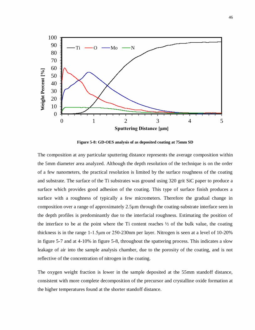
46
Figure 5-8: GD-OES analysis of as deposited coating at 75mm SD
The composition at any particular sputtering distance represents the average composition within
the 5mm diameter area analyzed. Although the depth resolution of the technique is on the order
of a few nanometers, the practical resolution is limited by the surface roughness of the coating
and substrate. The surface of the Ti substrates was ground using 320 grit SiC paper to produce a
surface which provides good adhesion of the coating. This type of surface finish produces a
surface with a roughness of typically a few micrometers. Therefore the gradual change in
composition over a range of approximately 2.5µm through the coating-substrate interface seen in
the depth profiles is predominantly due to the interfacial roughness. Estimating the position of
the interface to be at the point where the Ti content reaches ½ of the bulk value, the coating
thickness is in the range 1-1.5μmor250-230nm per layer. Nitrogen is seen at a level of 10-20%
in figure 5-7 and at 4-10% in figure 5-8, throughout the spattering process. This indicates a slow
leakage of air into the sample analysis chamber, due to the porosity of the coating, and is not
reflective of the concentration of nitrogen in the coating.
The oxygen weight fraction is lower in the sample deposited at the 55mm standoff distance,
consistent with more complete decomposition of the precursor and crystalline oxide formation at
the higher temperatures found at the shorter standoff distance.
0
10
20
30
40
50
60
70
80
90
100
0 1 2 3 4 5
Wei
gh
t P
erce
nt
[%]
SputteringDistance[μm]
Ti O Mo N

47
In both samples, especially for the sample deposited as 75mm standoff distance, the O/Mo ratio
was higher near the surface of the coating, then decreasing as sputtering continued. This behavior
may be explained by considering that the first layers deposited were exposed to the high
temperature during the subsequent torch passes, whereas the last layer deposited was not exposed
to additional heating from the torch.
5.2 Molybdenum oxide/nitride on stainless steel
5.2.1 Molybdenum oxide
The first attempts to fabricate a functional supercapacitor electrode employed stainless steel
substrates as in previous research conducted in CACT. Some capacitive behavior was observed
but very bad adhesion prevented reliable characterization of the electrode because the electrode
disintegrated into the solution after only 10 CV cycles. In order to understand the effect of
thermal history on the electrochemical performance, multiple samples were deposited using a
200μmdiametersolutionnozzleonpolishedstainlesssteelsubstrates.Fivelayersweredeposited
at 55, 60, and 65mm standoff distances with 5.3 and 8.3mm raster distances. Figure 5-9 displays
results of cyclic voltammetry at 100mV sec-1
scan rate of samplesdepositedatdifferentSD’s
with a constant RD, allowing comparison of the effect of substrate temperature on the
capacitance of the electrodes. Recall that features of good electrochemical performance for a
super capacitor would include a rectangular shaped CV curve and a large area of hysteresis. The
samples presented in figure 5-9 lack these features, although comparison with the curve showing
the bare substrate performance reveals that the electrodes are electrochemically active. There is
some charge accumulation indicated by the curves; the calculated capacitance is 129.77mF cm-2
for 55mm, 76.63mF cm-2
for 60mm and 66.55mF cm-2
for65mmSD.Howeverthe“cigar”shape
indicates that a large resistance is present in the samples and the charge accumulation is probably
not due to reversible surface phenomena such as EDLC and pseudo-capacitance but rather to
irreversible reactions with the electrode material. The electrochemical activity of the electrodes
increases as the standoff distance decreases, corresponding to a higher fraction of fully
decomposed molybdenum oxide phase.

48
Figure 5-9: Cycle voltammetry plots of as deposited samples at 55, 60, 65mm SD and 5.3mm RD
The thermal history of the coating is not determined only by the distance between the torch and
substrate, but rather can be affected by several types of process controls. Increasing the raster
distance from 5.3mm to 8.3mm means that covering the 12.5mm long sample takes fewer passes
than with a smaller RD, dramatically changing the thermal history. The lower exposure time
leads to lower temperature and less decomposition of the solution, resulting in lower fraction of
capacitive phases and lower capacity as shown in figure 5-10.
-40
-35
-30
-25
-20
-15
-10
-5
0
5
10
15
-0.6 -0.5 -0.4 -0.3 -0.2 -0.1 0
Cu
rren
t D
ensi
ty (
mA
cm
-2)
Cell Voltage (V)
55mm 65mm 75mm Substrate

49
Figure 5-10: Cyclic voltammetry of as deposited samples on stainless steel at different RD
The suggestion that the electrochemical activity observed for the samples was likely due to
irreversible reactions was confirmed by the results of extended cycling. After only 10 cycles the
coatings have almost completely disintegrated into the solution leaving dark blue flakes of
coating on the electrode, as shown in figure 5-11. The severe reactions with deposited coating
generated charge transfer but also destroyed the electrode.
Figure 5-11: As deposited coating on stainless steel substrate post CV
-30
-25
-20
-15
-10
-5
0
5
10
15
-0.6 -0.5 -0.4 -0.3 -0.2 -0.1 0
Cu
rren
t D
ensi
ty (
mA
cm
-2)
Cell Voltage (V)
Substrate 0.21RD,60SD 0.33RD.60SD

50
5.2.2 Molybdenum nitride
Establishing the thermal history concept and realizing the major effect it has on the deposited
electrode aided in understanding the behavior shown in the CV plots, but the fact that
molybdenum nitride is known to have a better electrochemical stability encouraged conducting
experiments on nitrided coatings deposited on stainless steel. Nitridation was performed on
samples deposited on polished stainless steel substrates at 55, 65 and 75mm SD and a 5.3mm
RD.Five layersweredepositedusinga150μm solution nozzleAmmoniagaswasused in the
thermal process (TRP) described in the procedure section. The cyclic voltammetry tests were
conducted in 0.5M solution of H2SO4, over a voltage range of -0.15 to 0.45V, at a scan rate of
100mV sec-1
with a Ag/AgCl counter electrode. From the plots shown in figure 5-12 it can be
seen that all the coatings showed the same non-capacitive behavior, as all plots are not
rectangular and the current does not go below zero indicating dissolution of the electrode,
leading to large resistance in the coating. The resistance is so high that the charge can only flow
in one direction.
Figure 5-12: Cyclic voltammetry testing on nitride samples deposited on stainless steel
Due to poor adhesion of the coating to the substrate surface and the stress induced by the
nitridation process, exposed substrate was generated. Cracks in the coating which reach the bare
-50
0
50
100
150
200
250
300
-0.2 -0.1 0 0.1 0.2 0.3 0.4 0.5
Cu
rren
t D
ensi
ty (
mA
cm
-2)
Cell Voltage (V)
55mm 65mm 75mm Substrate
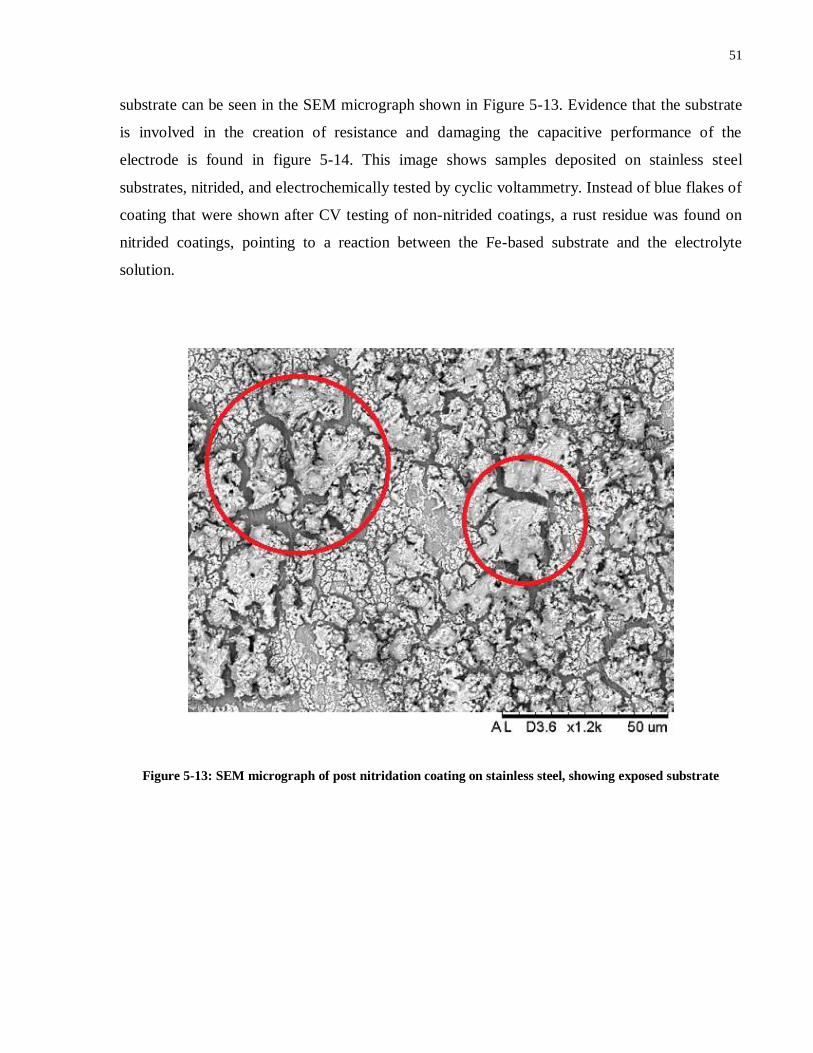
51
substrate can be seen in the SEM micrograph shown in Figure 5-13. Evidence that the substrate
is involved in the creation of resistance and damaging the capacitive performance of the
electrode is found in figure 5-14. This image shows samples deposited on stainless steel
substrates, nitrided, and electrochemically tested by cyclic voltammetry. Instead of blue flakes of
coating that were shown after CV testing of non-nitrided coatings, a rust residue was found on
nitrided coatings, pointing to a reaction between the Fe-based substrate and the electrolyte
solution.
Figure 5-13: SEM micrograph of post nitridation coating on stainless steel, showing exposed substrate

52
Figure 5-14: Post CV samples of nitrited coatings deposited on stainless steel at 55, 65 and 75mm SD
5.3 Molybdenum oxide/nitride on titanium
Because samples deposited on stainless steel substrates have produce very little capacitance with
poor stability, and nitrided coatings on the same substrate have showen no capacitance at all,
focus was directed to titanium substrates. These substrates have shown superior adhesion
properties with molybdenum oxide coatings in various literature sources, and other groups in the
Department of Materials Science and Engineering have reported much improved results using Ti
substrates.
5.3.1 Molybdenum oxide
A grade 2 titanium sheet 1mm in thickness was cut into the same 75×12.5mm samples as the
stainless steel and the same 320 grit polishing method was applied as an initial preparation stage.
In addition all torch and spraying parameters were kept the same in order the compare the
different substrate properties without introducing additional influencing parameters. In figure 5-
15 SEM micrographs of 2 samples deposited at 55mm and 75mm standoff distances are
presented. As in the as deposited samples on stainless steel, the Ti substrate samples show the
same dependence on the thermal history concept, with higher porosity visible on the sample
deposited at 75mm SD.

53
Figure 5-15: SEM micrographs of as deposited samples on Ti substrate
In order to understand if the substrate change has made a difference on the stability and
performance of the electrode, CV testing was performed on the as-deposited samples (figure 5-
16). The shape of the plots is not an ideal rectangular, indicating some cathodic and anodic
resistance is still present, however the shape is better than for the samples deposited on stainless
steel substrates suggesting that the stability is higher. The area for the sample deposited at 55mm
is the largest, followed by the samples deposited at 65mm and 75mm SD. The calculated
capacitance was of 104 mF cm-2
, 80mF cm-2
and 71mF cm-2
, respectively. Based on the XRD
results of coatings deposited on stainless steel substrates under these conditions, molybdenum
oxideintheformofα-MoO3 is present in a higher fraction in coatings deposited at shorter SD.
The larger area inside the CV plot indicating larger charge accumulation therefore correlates
with the amount of the desirable electrochemically active phase.
In order to understand the short term stability of the coatings, the samples were cycled for 100
cycles at 1V sec-1
, then 5 additional cycles at 100mV sec-1
, after which the capacitance
measurement was performed again. The results are shown in figure 5-17 for a sample deposited
at 75mm SD. The reduction in capacitance was 26% after 100 cycles illustrating that the samples
still unstable; some reaction is creating resistance and reducing the capacitance. The CV results
for samples deposited at 55 and 65mm SD are similar, with reductions in capacitance of 25% and
22% respectively, after 100 cycles.

54
Figure 5-16: Cyclic voltammetry testing for as-deposited samples on Ti substrate
Figure 5-17: CV plot of as deposited sample at 75mm SD after 4 and 104 cycles
-40
-30
-20
-10
0
10
20
30
-0.6 -0.5 -0.4 -0.3 -0.2 -0.1 0
Cu
rren
t D
ensi
ty (
mA
cm
-2)
Cell Voltage (V)
55mm 65mm 75mm
-25
-20
-15
-10
-5
0
5
10
15
-0.6 -0.5 -0.4 -0.3 -0.2 -0.1 0
Cu
rren
t D
ensi
ty (
mA
cm
-2)
Cell Voltage (V)
75mm (4 cycle)
75mm (104 cycle)

55
Higher magnification SEM examination of the samples reveals that the grain size is very small,
(figure 5-18) agreeing with the peak broadening calculation presented in previous sections, and is
probably responsible for the large capacitance of the as-deposited samples on Ti substrates. The
small grain size illustrates one of the biggest advantages of the SPPS method when compared
with a simple heat treatment of molybdenum salt precursor at 700°C for 1hr (figure 5-19), where
verylargegrainsof50μmareachievedwithverysharpα-MoO3 peaks in the XRD pattern.
Figure 5-18
Figure 5-18: High magnification SEM micrograph of as deposited sample of Ti substrate

56
Figure 5-19: Molybdenum oxide solution after 1hr at 700c heat treatment
5.3.2 Molybdenum nitride
In order to make the electrode more stable, the samples were nitrided using ammonia gas under
the programed thermal profile presented in the experimental procedure section. Figure 5-20
shows SEM micrographs of samples deposited at 55 and 75mm SD. The images illustrate the
island microstructure that was created after the thermal treatment.

57
Figure 5-20: SEM micrographs of nitrided samples deposited at 55mm and 75mm SD
Figure 5-21: High magnification SEM micrographs of post nitridation sample deposited at 55mm SD
To investigate if the area between the large islands was exposed substrate, as observed for nitride
coatings on stainless steel substrates, EDS was performed on islands and on the area between
islands. According to the results presented in figure 5-22, the area between the islands has a
Mo/N ratio consistent with Mo2N3, which is a phase usually created in thin films of molybdenum
nitride [42]. No peaks associated with the Ti substrate were observed, indicating this area was
fully covered by the molybdenum nitride. The Mo/N ratio for the island was high, indicating the
presenceofothernitridephasessuchasγ-Mo2N0.92,γ-Mo2N,and/orδ-MoN.

58
Figure 5-22: EDS analysis of sample deposited at 55mm SD (a) on island (b) between islands
As seen in figure 5-20, the different thermal histories of the coatings deposited at 55mm and
75mm SD prior to nitridation has resulted in differences in the coating microstructure after
nitridation. The XRD patterns presented in figure 5-23 (Mo2N-PDF #00-025-1366, Ti-PDF #00-
001-1197)showthatthemost intensepeaksofmolybdenumnitridephasessuchasγ-Mo2N0.92,
γ-Mo2N, δ-MoN are larger relative to the major peak for MoO3 for the coating deposited at
75mm SD than for the coating deposited at 55mm SD. The calculated phase fractions indicate
that nitride phases make up 91% on the coating deposited at 75mm SD and 46% of coating
deposited at 55mm SD. The higher temperatures experienced during deposition by the coating
deposited at a standoff distance of 55mm resulted in more completed decomposition of the
precursorandahigher fractionofα-MoO3 in the coating than for coatings deposited at longer
standoff distances. It appears that transformation of the molybdenum oxides into the nitride
phasesismoredifficultincoatingswherethecrystallizationofα-MoO3 has been extensive.

59
Figure 5-23: XRD patterns of nitrided samples deposited on Ti substrate
The results of cyclic voltammetry testing of the nitride electrodes are presented in figure 5-24.
Three samples deposited at 55, 65 and 75mm were cycled at 100mV sec-1
in 0.5M H2SO4 against
a Ag/AgCl reference electrode. The nearly rectangular shape of the curve indicates that the
samples are stable and reversible in terms of electrochemical cycling, with a low resistance. The
capacitance of the nitrided samples deposited at the three standoff distances was inverted
compared to the capacitance of the as-deposited samples. Samples deposited at 75mm SD have a
calculated capacitance of 62.4 mF cm-2
, but at the shorter SD distances the capacitance is 42 and
25.2mF cm-2
for 65 and 55mm SD respectively. The increase in capacitance with increased
standoff distance correlates with the increase in the fraction of nitride phases at longer standoff
distances.
In order to investigate the stability of the nitrided electrodes, samples that were deposited at the
three different SD have been cycled 100 times with a 1V sec-1
scan rate, and then again for 5
cycles at 100mV sec-1
as was done for the as-deposited coatings. The reduction in capacitance
was 14%, 11%, 9% for the 55, 65 and 75mm standoff distances, respectively. This reduction is
more than 10% lower than the reduction observed for as-deposited samples on Ti after 100
cycles.
Although the shape of the CV curves for the nitrided samples is closer to the ideal rectangular
shape than the curves for the as-deposited samples, the capacitance of the as-deposited (oxide)
0 20 40 60 80 100
Inte
nsa
ty
2θ
75mm
55mm
Mo2N
[111]
Mo2N
[200]
Ti
Ti Ti
Ti
MoO3
[020] [110] [040] [021]
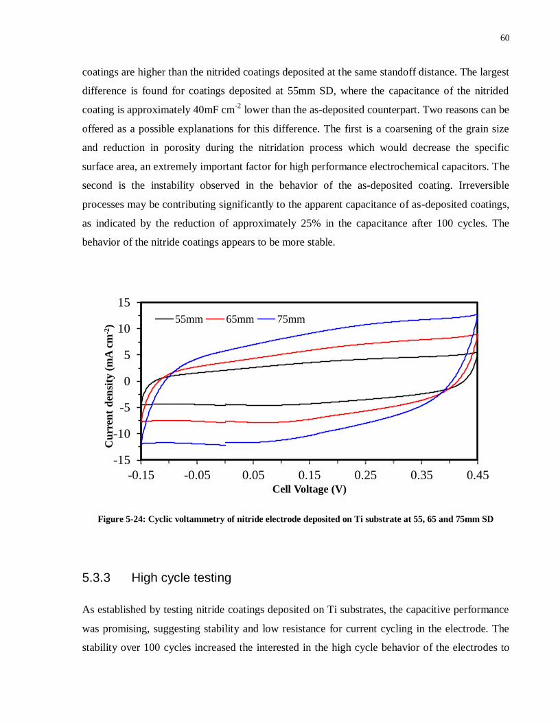
60
coatings are higher than the nitrided coatings deposited at the same standoff distance. The largest
difference is found for coatings deposited at 55mm SD, where the capacitance of the nitrided
coating is approximately 40mF cm-2
lower than the as-deposited counterpart. Two reasons can be
offered as a possible explanations for this difference. The first is a coarsening of the grain size
and reduction in porosity during the nitridation process which would decrease the specific
surface area, an extremely important factor for high performance electrochemical capacitors. The
second is the instability observed in the behavior of the as-deposited coating. Irreversible
processes may be contributing significantly to the apparent capacitance of as-deposited coatings,
as indicated by the reduction of approximately 25% in the capacitance after 100 cycles. The
behavior of the nitride coatings appears to be more stable.
Figure 5-24: Cyclic voltammetry of nitride electrode deposited on Ti substrate at 55, 65 and 75mm SD
5.3.3 High cycle testing
As established by testing nitride coatings deposited on Ti substrates, the capacitive performance
was promising, suggesting stability and low resistance for current cycling in the electrode. The
stability over 100 cycles increased the interested in the high cycle behavior of the electrodes to
-15
-10
-5
0
5
10
15
-0.15 -0.05 0.05 0.15 0.25 0.35 0.45
Cu
rren
t d
ensi
ty (
mA
cm
-2)
Cell Voltage (V)
55mm 65mm 75mm

61
understand the potential of high surface area molybdenum nitride electrodes deposited SPPS.
The midrange electrode deposited at 65mm SD on Ti substrate and nitride in ammonia was
cycled over 5000 cycles at a voltage sweep rate of 1V sec-1
. Every 1000 cycles the electrode was
subjected to a slower scant rate of 100mV sec-1
for 10 cycles. Figure 5-25 shows CV plots of the
samples at the beginning, after 1000 cycles and after 5000 cycles. The stable, almost rectangular
shape is remains indicating that the behaviour is reversible with low resistance, but a reduction in
area inside the plot is also indicates a loss in capacitance.
Figure 5-25: High cycle CV plot of nitrided sample deposited on Ti substrate
Although the overall capacitance reduction is 28%, the reduction between the first cycles and
1000 cycles is 22%, emphasizing that most of the reduction accrued in the in the first 1000
cycles. If the capacitance in plotted versus the number cycles a flatting trend is apparent. The
reduction flattens in an almost exponential rate to the point where the reduction between 4000
and 5000 cycles is 0.15% as shown in figure 5-26.
The reasons for the initial reduction in capacitance are not fully understood. Possibilities include
the elimination of reactive phases in the coating or impurities that may have accumulated during
the various stages of the process: deposition, transformation, or preparation of samples for CV
testing.
-8
-6
-4
-2
0
2
4
6
8
-0.15 -0.05 0.05 0.15 0.25 0.35 0.45
Cu
rren
t d
ensi
ty (
mA
cm
-2)
Cell Voltage (V)
Cycle #1
Cycle #1000
Cycle #5000

62
Figure 5-26: Capacitance as a function of cycle number for sample deposited at 65mm SD
5.4 Titanium electrode modification
In order to understand better how different process parameters influence the electrochemical
performance of the Mo oxide and nitride coatings, a series of process modifications were
investigated. Since no other group has reported the use of SPPS for deposition of these types of
coatings, ideas have been borrowed from work involving other deposition methods and applied
to our SPPS process. The following section describes how process modifications such as
substrate surface treatment, variation in coating thickness, and use of different gases in the oxide
to nitride conversion treatment influenced the electrochemical performance of electrodes
deposited by SPPS.
5.4.1 Substrate surface modification
There are reports in the literature [54] that in spray pyrolysis deposition, cleaning and nitridation
treatment of the Ti surface prior to deposition has reduced the remnant molybdenum oxide
fraction after nitridation and increased the capacitance. In order to see if surface modification has
an effect on samples deposited by SPPS, three sets of samples were prepared. The first are Ti
25
30
35
40
45
0 1000 2000 3000 4000 5000
Cap
acit
ance
(m
F cm
-2)
Cycle Number
Capacitance
Log. (Capacitance)

63
substrates polished as described previously, the second are Ti substrates polished and then
cleaned by Alcohol (Commercial Alcohols), Acetone ( (CH3)2CO, CALEDON) following by
immersion in 0.1M Hydrochloric acid (HCl, J.T.Baker) at 90°C for 10 Minutes in order to
remove organics and surface oxides in order to increase surface adhesion. The third set was
cleaned in the same way described above , but then also nitrided inside a tube furnace at 700°C
for 1Hr in ammonia gas (4.5 Grade, Praxair) flowing at 0.115 mL sec-1
. Samples were deposited
at 55, 65 and 75mm SD with a 5.3mmRD,usinga150μmdiameterliquidinjectionnozzle.
Figure 5-27: Cyclic voltammetry of (a) Cleaned Ti substrate (b) Cleaned and nitrided Ti substrate
In figure 5-27 CV plots of nitride coatings deposited on the modified Ti substrate surfaces are
presented. The rectangular shape of the CV curve is still present, but unlike coatings deposited
on polished Ti substrates which showed an approximately linear increase in capacitance with
increasing SD, coatings deposited at 55mm SD on polished and cleaned substrates exhibited a
lower capacitance then those deposited at 65 and 75mm SD. For coatings deposited on polished,
cleaned and nitrided substrates, the capacitance for the coating deposited at 75mm SD is much
higher than for coatings deposited at 55mm or 65mm SD. This behavior, shown in figure 5-28, is
not well understood. Additional experiments would be required to confirm the behaviour. In
general, no significant change in capacitance has been proven, and coatings deposited on
polished Ti substrates perform as well or better than coatings deposited on the modified surfaces.

64
Figure 5-28: Capacitance as a function of standoff distance for different surface modifications
5.4.2 Coating thickness modification
In order to understand the effect that coating thickness has on the electrochemical performance
of the electrode, a thinner, 3 layer, set of electrodes was deposited at 55, 65 and 75mm SD with a
150μmliquidinjectionnozzleonpolishedTisubstratesandthenconvertedbyheattreatmentin
ammonia gas. According to the thermal history concept developed in previous sections, fewer
passes of the torch over the sample would result in a lower substrate temperature and a shorter
time of exposure to elevated temperatures. The expectation under such conditions would be that
the sample would have a higher fraction of incompletely decomposed phases of the molybdenum
precursorandalowerfractionofα-MoO3 in the coating than in the 5 layer coatings, creating a
situation leading to a higher fraction of nitride phases after the ammonia heat treatment. The
fraction of nitrided phases was found to be 95%, 97%, and 92% for coatings deposited at 55, 65
and 75mm SD, respectively. The difference in the fraction of nitrided phases in coatings
deposited at 55mm and 65mm SD is likely not significant, however the fraction of nitride phases
in the coating deposited at 75mm SD slightly lower. This is not consistent with the trends seen in
the 5 layer coatings, but may be within the range of experimental variability.

65
The electrochemical behaviour of theses coatings shown in the CV curves plotted in figure 5-29
are similar. The coating deposited at the 65mm SD has the largest hysteresis area, indicating the
largest capacitance. The calculated capacitance values are 8.5, 13.3, and 8mF cm-2
for the
coatings deposited at standoff distances of 55, 65 and 75mm, which correlates with the nitride
fraction in the coatings, although the differences are small. Overall the capacitance values are
lower than found for the 5 layer samples. This could be due to a lower total surface area in the 3
layer coatings simply due to less material being present on the substrate.
Figure 5-29: Cyclic voltammetry of 3 layer deposition
5.4.3 Converting gas modification
The gas used in the oxide to nitride conversion process was changed from NH3 to N2 in response
to results reported by another group in the Materials Science and Engineering Department [64].
An additional set of samples was deposited with the same 5 layer coating conditions that were
employed before. The same thermal profile was used as previously for the oxide to nitride
transformation process, however NH3 was replaced by N2. The low resolution SEM image in
figure 5-30 reveals a completely different microstructure to the one obtained using NH3 in the
-4
-3
-2
-1
0
1
2
3
4
-0.15 -0.05 0.05 0.15 0.25 0.35 0.45
Cu
rren
t d
ensi
ty (
mA
cm
-2)
Cell Voltage (V)
55mm 65mm 75mm

66
process. The microstructure consisted of small, angular particles scattered over the surface of the
substrate. Higher magnification images of this structure reveal faceted, roughly equiaxed
particles 1-3μmacross.
Figure 5-30: Low resolution SEM image of sample deposited at 75mm SD and heat treated in N2
Figure 5-31: high resolution SEM micrographs of samples heat treated by N2
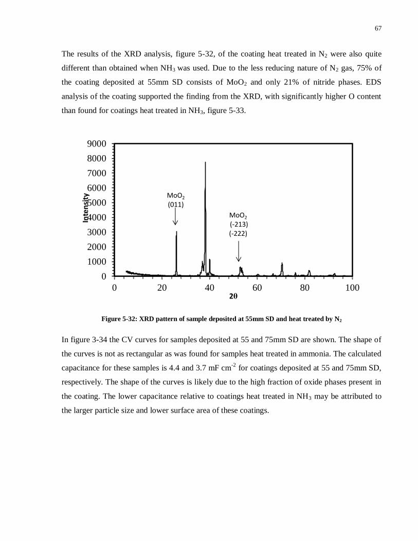
67
The results of the XRD analysis, figure 5-32, of the coating heat treated in N2 were also quite
different than obtained when NH3 was used. Due to the less reducing nature of N2 gas, 75% of
the coating deposited at 55mm SD consists of MoO2 and only 21% of nitride phases. EDS
analysis of the coating supported the finding from the XRD, with significantly higher O content
than found for coatings heat treated in NH3, figure 5-33.
Figure 5-32: XRD pattern of sample deposited at 55mm SD and heat treated by N2
In figure 3-34 the CV curves for samples deposited at 55 and 75mm SD are shown. The shape of
the curves is not as rectangular as was found for samples heat treated in ammonia. The calculated
capacitance for these samples is 4.4 and 3.7 mF cm-2
for coatings deposited at 55 and 75mm SD,
respectively. The shape of the curves is likely due to the high fraction of oxide phases present in
the coating. The lower capacitance relative to coatings heat treated in NH3 may be attributed to
the larger particle size and lower surface area of these coatings.
0
1000
2000
3000
4000
5000
6000
7000
8000
9000
0 20 40 60 80 100
Inte
nsi
ty
2θ
MoO2 (011)
MoO2
(-213) (-222)

68
Figure 5-33: EDS analysis of sample transformed in N2
Figure 5-34: Cyclic voltammetry plot of samples transformed by N2
-1.5
-1
-0.5
0
0.5
1
1.5
-0.15 0.05 0.25 0.45
Cu
rren
t d
ensi
ty (
mA
cm
-2)
Cell Voltage (V)
55mm 75mm

69
Chapter 6: Conclusions and Future Work
The objective of this thesis was to explore and demonstrate the concept of high surface area
molybdenum oxide/nitride electrodes for electrochemical capacitor application deposited by
SPPS. Several critical deposition parameters, substrate material and oxide to nitride
transformation cycles were investigated in order to determine the overall process performance
and compatibility for industrial application.
1. Molybdenum oxide was successfully deposited by SPPS on stainless steel substrates
revealing a high surface area, sub-microngrain sizeand a varietyofα-MoO3 fractions
depending on the substrate to torch distance (SD).
2. Standoff distance, raster distance and solution injection rate have a great effect on
substrate temperature which affects the decomposition of the precipitates and
intermediate products, creating changes in the microstructure and phase composition of
the coating.
3. The variation in the phase composition and microstructure directly affect the
electrochemical performance, closely linking the process control of the deposition to the
electrode performance.
4. Oxide coatings on stainless steel were found to have some apparent capacitive behaviour
generated from unstable electrochemical activity on the electrode surface. The coatings
completely disintegrated after only 10 CV cycles.
5. Transformation of the oxide coating on stainless steel into nitride by a multiple stage heat
treatment with flowing ammonia gas resulted in the formation of cracks in the coating
and exposed the substrate, resulting in very high electrode resistance and no charge
accumulation.
6. Changing the substrate material to titanium for molybdenum oxide electrodes increased
the coating adhesion substantially, stabilised the electrode and resulted in high
capacitance, but due to the electrochemical nature of Mo oxide the CV plot is not
rectangular and some resistance is still present in the coating.

70
7. Nitriding the molybdenum oxide coating on titanium created a very stable, low
resistance, rectangular shaped CV curve, extremely desirable for electrochemical
applications.
8. Unlike oxide coatings for which shorter standoff distances and higher substrate
temperatures have resulted in better electrochemical performance due to a larger fraction
ofα-MoO3, nitride coating have shown higher capacitance for longer standoff distances
due to more extensive transformation from oxide phases into nitride phases.
9. A schematic illustration of the electrode dependence on thermal history and deposition
parameters is shown in figure 6-1, were the thermal history concept is presented for the
oxide and nitride coatings.
10. High cycle testing of electrodes deposited on titanium by SPPS at a standoff distance of
showed good performance during the 5000 cycles, with a total of 28% reduction in
capacitance and a final capacitance of 30mF cm-2
over the 5000 cycles. The behaviour
stabilized with increased cycles: the capacitance decreased by 22% after the first 1000
cycles, but by only 0.15% for cycles 4000 to 5000.
11. Process modifications such as changes in substrate preparation, changes in deposition
thickness and gas used for conversion into nitride did not improve the performance of the
electrode, but rather decreased the capacitive performance.
12. SPPS was shown to be an effective, simple, process for the deposition of molybdenum
nitride electrodes. The potential for scale up to industrial applications is favored by
deposition under atmospheric conditions and the ability to deposit on sheet substrates in a
reel to reel configuration.

71
Figure 6-1: Schematic flow chart for better capacitance performance for oxide and nitride coatings
6.1 Future work
1. The injection system was a very simplistic design and was the weak link in deposition
process, clogging and reducing the level of control over sample deposition, as many
commercially available injection systems are offering high level of control and automated
stirring and temperature control of the solution.
2. The injection process and torch configuration allowed only radial injection intensifies the
over and under spray phenomena reducing the control over the process, but torch
manufacturer have introduced axial injected torches that are available in the CACT.
3. GD-OES analysis of electrodes deposited on stainless steel in order to oxygen and
nitrogen distribution in the coating, understanding better the thermal history concept and
the affect and the adhesion between the coating and substrate.
4. SEM, EDS and XPS of coating cross sections to investigate the bonding and phase
formation at the coating-substrate interface and better understanding the adhesion
properties.
Oxide
•Short SD
•high substrate temprature
•high rate of decompoistion
•small fraction of undecomposed phases
•higher capacitance
Nitride
•long SD
•lower substrate temprature
•low rate of decomposition
•large faction undecomposed phases
•higher capacitance

72
5. Better calculation of capacitance as a function of surface area based on BET analyses for
comparison with literature results.
6. Additional experimentation is needed in order to fine tune the process parameters and
electrochemical performance.
7. High cycling was conducted for mid-range molybdenum nitride electrode, other high
cycling experiments are needed in order to determine what the optimum process is for
deposition, in addition, higher cycling such as 10K and 50K is required to determine long
term stability.

73
References
[1] American Society for Metals Vol. 1 No. 2 (1980) 83-86.
[2] M. Atesa, T. Karazehira, A.S. Saracb, Curr. Physical Chem. 2 (2012) 224-240.
[3] W. Baoxing, D. Shaojun, J. of Electroanalytical Chem. 379 (1994) 207-214.
[4] S. Basu, B.M. Cetegen, Int.J.Heat Mass Transfer 50 (2007) 3278-3290.
[5] S. Basu, E.H. Jordan, B.M. Cetegen, J Therm Spray Tech 17 (2008) 60-72.
[6] O. Bertrand, L.C. Dufour, Phys.Stat.Sol.(a) 60 (1980) 507-519.
[7]B.L.Bramfitt,7.MetallographicSpecimenPreparation,Metallographer’sGuide- Practices
and Procedures for Irons and Steels, 2002, pp. 199.
[8] T. Brezesinski, M. Groenewolt, N. Pinna, H. Amenitsch, M. Antonietti, B. Smarsly, Adv
Mater 18 (2006) 1827-1831.
[9] T. Brezesinski, J. Wang, S.H. Tolbert, B. Dunn, Nat. Mater. 9 (2010) 146-151.
[10] A. Burke, J.Power Sources 91 (2000) 37-50.
[11] A.F. Burke, Proc IEEE 95 (2007) 806-820.
[12] A.G. Cairns, J.G. Gallagher, J.S.J. Hargreaves, D. Mckay, E. Morrison, J.L. Rico, K.
Wilson, J.Alloys Compounds 479 (2009) 851-854.
[13] C. Chen, D. Zhao, X. Wang, Materials Chemistry & Physics 97 (2006) 156-161.
[14] C. Chen, D. Zhao, D. Xu, X. Wang, Mater. Chem. and Phys. 95 (2006) 84-88.
[15] D. Chen, E.H. Jordan, M. Gell, Surf.Coat.Technol. 202 (2008) 2132-2138.
[16] J. Chmiola, C. Largeot, P.L. Taberna, P. Simon, Y. Gogotsi, Angew. Chem. Int. Ed. 47
(2008) 3392 –3395.

74
[17] D. Choi, G.E. Blomgren, P.N. Kumta, Advanced Mater. 18 (2006) 1178-1182.
[18] D. Choi, P.N. Kumta, J. of Electrochem. Soc. 153 (2006) A2298-A2303.
[19] J. Choi, R.L. Curl, L.T. Thompson, Journal of Catalysis 146 (1994) 218-227.
[20] J. Choi, R.L. Curl, L.T. Thompson, Journal of Catalysis 146 (1994) 218-227.
[21] N.A. Choudhury, A.K. Shukla, S. Sampath, S. Pitchumanic, J. of the electrochem. Soc. 153
(2006) A614-A620.
[22] J. Christopher.H, M. James.N, S. Angelica.M, Chem. Mater. 2 (1990) 150–157.
[23] B.E. Conway, Electrical Double-Layer and Ion Adsorption Behavior at Solid–Solution
Interfaces, Encyclopedia of Surface and Colloid Science, Second Edition, Taylor & Francis,
2011, pp. 1908-1931.
[24] B.G. Demczyk, J.G. Choi, L.T. Thompson, Appl. Surf. Sci. 78 (1994) 63-69.
[25] W. Dong, B. Dunn, J. of Non-Crystalline Solids 225 (1998) 135-140.
[26] P. Fauchais, J. Phys. D: Appl. Phys. 37 (2004) R86–R108.
[27] P. Fauchais, A. Joulia, S. Goutier, C. Chazelas, M. Vardelle, A. Vardelle, S. Rossignol, J. of
Phys. D: Appl. Phys. 46 (2013) 1-14.
[28] P. Fauchais, G. Montavon, R.S. Lima, B.R. Marple, J. Phys. D: Appl. Phys. 44 (2011) 1-53.
[29] P. Fauchais, G. Montavon, M. Vardelle, J. Cedelle, Surf.Coat.Technol. 201 (2006) 1908-
1921.
[30] P. Fauchais, V. Rat, J.F. Coudert, R. Etchart-Salas, G. Montavon, Surf.Coat.Technol. 202
(2008) 4309-4317.
[31] M. Golozar, K. Chien, T.W. Coyle, J. of Therm. Spray Technol. 21 (2012) 469-479.
[32] M. Golozar, K. Chien, K. Lian, T. Coyle, J Therm Spray Tech 22 (2013) 710-722.

75
[33] A. Guerfi, R.W. Paynter, L.H. Dao, Journal of the Electrochemical Society [H.W.Wilson -
AST] 142 (1995) 3457.
[34] C.C. Hu, Y.H. Huang, J. of Electrochem. Soc. 146 (1999) 2465-2471.
[35] J. Huang, B. Sumpter, V. Meunier, Chem. Eur. J. 14 (2008) 6614-6626.
[36] T. Ivanova, A. Szekeres, M. Gartner, D. Gogova, K.A. Gesheva, Electrochim.Acta 46
(2001) 2215-2219.
[37] M. Jayalakshmi, K. Balasubramanian, Int. J. Electrochem. Sci 3 (2008) 1196 - 1217.
[38] I.H. Kim, K.B. Kim, J. of the electrochem. Soc. 153 (2006) A383-A389.
[39] R. Ko¨tz, M. Carlen, Electrochimica Acta 45 (2000) 2483-2498.
[40] S. Kühn, P. Schmidt-Zhang, A.H. Hahn, M. Huber, M. Lerch, T. Ressler, Chem. Cent. J. 5
(2011) 1-10.
[41] E. Lalik, W.I.F. David, P. Barnes, J.F.C. Turner, The Journal of Physical Chemistry B 105
(2001) 9153-9156.
[42] K.H. Lee, Y.W. Lee, A.R. Ko, G. Cao, K.W. Park, J. Am. Ceram. Soc. 96 (2013) 37-39.
[43] C. Li, H. Zhang, K. Wang, Y. Miao, Q. Xin, Appl. Spectroscopy 47 (1993) 56-61.
[44] X. LI, Y. Xing, H. Wang, H. Wang, W. Wang, X. Chen, Transactions of Nonferrous Metals
Society of China 19 (2009) 620-625.
[45] K. Lian, C.M. Li, Electrochem. Commun. 11 (2009) 22-24.
[46] T.C. Liu, W.G. Pell, B.E. Conway, S.L. Roberson, J. of Electrochem. Soc. 145 (1998) 1882-
1888.
[47] T.M. McEvoy, K.J. Stevenson, J.T. Hupp, X. Dang, Langmuir 19 (2003) 4316-4326.
[48] D. Mutschall, K. Holzner, E. Obermeier, Sensors Actuators B: Chem. 36 (1996) 320-324.
[49] T. Nelis, J. Pallosi, Appl. Spectroscopy Reviews 41 (2006) 227-258.

76
[50] P. Pande, P.G. Rasmussen, L.T. Thompson, J. Power Sources 207 (2012) 212– 215.
[51] L. Pawlowski, Surf.Coat.Technol. 203 (2009) 2807-2829.
[52] D. Pech, M. Brunet, H. Durou, P. Huang, V. Mochalin, Y. Gogotsi, P.L. Taberna, P. Simon,
Nat. Nanotechnol. 5 (2010) 651-654.
[53] L. Pershin, L. Chen, J. Mostaghimi, J. of Therm. Spray Technol. 17 (2008) 608-611.
[54] L. Pershin, L. Chen, J. Mostaghimi, International Therm. Spray Conference (2007) 266-269.
[55] H. Philippe, M. Charles, Millennium Steel (2011) 357-360.
[56] M.J.N. Pourbaix, Atlas of electrochemical equilibria in aqueous solutions, [1st English ed.]
ed., Pergamon Press|c[1966], Oxford-Pergamon Press [1966]; 1966.
[57] S.L. Roberson, D. Finello, R.F. Davis, Materials Science & Engineering A 248 (1998) 198-
205.
[58] S.L. Roberson, D. Finello, R.F. Davis, J. of Appl. Electrochem. 29 (1999) 75-80.
[59] J.F. Rusling, S.L. Suib, Adv Mater 6 (1994) 922-930.
[60] Y. Saito, C. Kaito, T. Naiki, J.Cryst.Growth 79 (1986) 436-442.
[61] R. Signorelli, D.C. Ku, J.G. Kassakian, J.E. Schindall, Inst. of Electrical and Electronics
Eng. 97 (2009) 1837-1847.
[62] P. Simon, Y. Gogotsi, Nat. Mater. 7 (2008) 845-854.
[63] W. Sugimoto, T. Ohnuma, Y. Murakami, Y. Takasu, Electrochem. and Solid-State Letters 4
(2001) A145-A147.
[64] Y. Ting, K. Lian, N. Kherani, ECS Transactions 35 (2011) 133-139.
[65] M. Vardelle, A. Vardelle, P. Fauchais, M.I. Boulos, AIChE J. 29 (1983) 236-243.
[66] S.S. Viswanathan, L. Chi-Woo, Chem Sus Chem 5 (2012) 1146 – 1161.

77
[67] L. Volpe, M. Boudart, J. of solid State Chem. 59 (1985) 332-347.
[68] L. Volpe, M. Boudart, Catal. Rev.-Sci. Eng. 27(4) (1985) 515-538.
[69] B. Wiecek, U. Twardoch, Journal of Physics and Chemistry of Solids 65 (2004) 263-268.
[70] J. Wienold, R.E. Jentoft, T. Ressler, Eur.J.Inorg.Chem. 2003 (2003) 1058-1071.
[71] R.S. Wise, E.J. Markel, Journal of Catalysis 145 (1994) 344-355.
[72] W. Xing, S.Z. Qiao, R.G. Ding, F. Li, G.Q. Lu, Z.F. Yan, H.M. Cheng, Carbon 44 (2006)
216-224.
[73] B. Xu, F. Wu, S. Chen, C. Zhang, G. Cao, Y. Yang, Electrochim.Acta 52 (2007) 4595-4598.
[74] X.h. Yang, Y.g. Wang, H.m. Xiong, Y.y. Xia, Electrochim.Acta 53 (2007) 752-757.
[75] Z.L. Yin, X.H. Li, Q.S. Zhao, S.Y. Chen, G.R. Liu, S.Q. Wang, Thermochimica Acta 244
(1994) 283-289.
[76] Z. Yin, X. Li, Q. Chen, Thermochimica Acta 352 (2000) 107–110.
[77] Y. Zhang, H. Feng, X. Wu, L. Wang, A. Zhang, T. Xia, H. Dong, X. Li, L. Zhang, Internatl.
J. of Hydrog. energy 34 (2009) 4889-4899.
[78] J.P. Zheng, P.J. Cygan, T.R. Jow, J. of Electrochem. Soc. 142 (1995) 2699-2703.