high band width circuit techniques for cmos-rf
TRANSCRIPT

UNIV TEL AVIV M. Moyal1
High Band Width Circuit Techniques for CMOS-RFHigh Band Width Circuit Techniques for CMOS-RF

UNIV TEL AVIV M. Moyal2
Agenda
1) Applications for High Speed Design
2)Feed Backs
3) Inductors as BW boosters
4) CMOS “ Synthesized Inductors”
5) High Speed Buffers- Cherry Hopper and CTLE
6) “RF” ADCs for 10GS/s
1) Applications for High Speed Design
2)Feed Backs
3) Inductors as BW boosters
4) CMOS “ Synthesized Inductors”
5) High Speed Buffers- Cherry Hopper and CTLE
6) “RF” ADCs for 10GS/s

UNIV TEL AVIV M. Moyal3
1) Applications for High Speed Design
UNIV TEL AVIV M. Moyal4
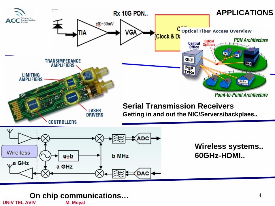
APPLICATIONS
Serial Transmission Receivers Getting in and out the NIC/Servers/backplaes..
Wireless systems.. 60GHz-HDMI..
On chip communications…
UNIV TEL AVIV M. Moyal5
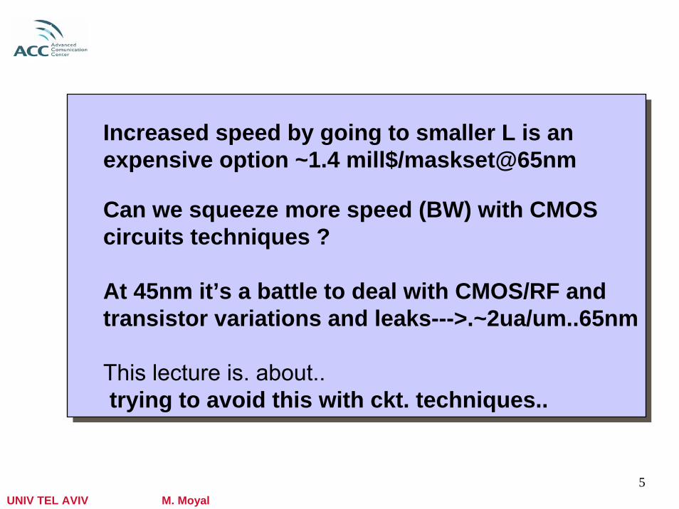
Increased speed by going to smaller L is an expensive option ~1.4 mill$/maskset@65nm
Can we squeeze more speed (BW) with CMOS circuits techniques ?
At 45nm it’s a battle to deal with CMOS/RF and transistor variations and leaks--->.~2ua/um..65nm
This lecture is. about..trying to avoid this with ckt. techniques..

UNIV TEL AVIV M. Moyal6
2) Feed backs to boost BW

UNIV TEL AVIV M. Moyal7
Basic Feed back to boost BW
t/RCe-Vin[1 Vout(t) −
=
CR∗=τ )1/()( +∗= ACRnew τ
VinVout
A
VoutAVy ∗=
R
C
R
C
1)/RCt(A-e-1 [ Vin Vout(t)
+=
1+A
1)}RSC/(A1/{1 Vout/Vin ++=

UNIV TEL AVIV M. Moyal8
Simulation: a=2 and a=10
Ac response Time domain
)(/ fViVo
Frequency
ac TF RC/fdback )(/ fViVo
Time
Step response
)(/ fViVo

UNIV TEL AVIV M. Moyal9
CSA
R1=n*R2
C1
C2=n*C1
R2
R3
IoutIin
Gain dB
Freqω
Closed loop op-ampMain pole @ R1C1
Zero of PZ cancelation net @ R2C2
Total BW of CSA stage pole @ R3C2
IinIo/
The Math: Transfer function with ideal opamp.H1(s)=R1/(1+R1C1S). One pole at -1/R1C1
The zero part is H(s)=(1+R2C2S)/(R2+R3+R2R3C2S)a zero at -1/R2C2=-1/R1C1 and a pole at –(R2+R3)/(R2R3C2)Combination of these two cancels the pole leaving R1/(R2+R3+R2R3C2S) one pole. When R3<<R2 this reduces to a pole at -1/R3C2. with gain of R1/R2=n
Basic Feed back to boost BWIn X ray detection…
Frequency
)(1 SH

UNIV TEL AVIV M. Moyal10
Problem remain: We need “open loop” structure or very fast feedback to go beyond GHz speed
A Solution: lets look at Transistors and passives elements since they are the fastest basic block we got.

UNIV TEL AVIV M. Moyal11
3) Inductors as BW boosters
UNIV TEL AVIV M. Moyal12
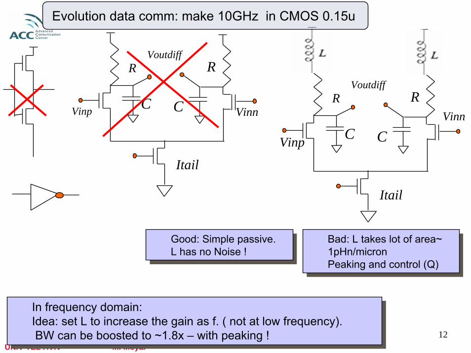
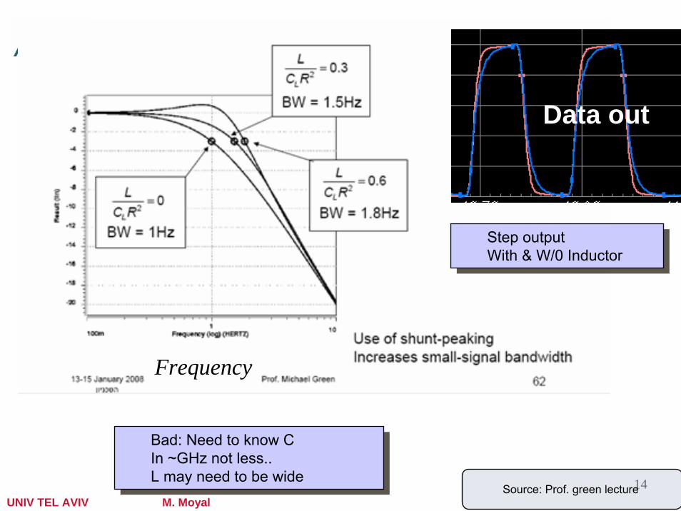
In frequency domain: Idea: set L to increase the gain as f. ( not at low frequency). BW can be boosted to ~1.8x – with peaking !
In frequency domain: Idea: set L to increase the gain as f. ( not at low frequency). BW can be boosted to ~1.8x – with peaking !
Bad: L takes lot of area~ 1pHn/micronPeaking and control (Q)
Bad: L takes lot of area~ 1pHn/micronPeaking and control (Q)
Good: Simple passive.L has no Noise !
Good: Simple passive.L has no Noise !
R
C
R
CVinp Vinn
Itail
Voutdiff
R
C
R
CVinp
Itail
Voutdiff
Vinn
Evolution data comm: make 10GHz in CMOS 0.15u

UNIV TEL AVIV M. Moyal13Source: Prof. green lecture
VCC
R R
IssVbias
inp innoutnoutp
M1
M2 M3
UNIV TEL AVIV M. Moyal14
Bad: Need to know CIn ~GHz not less..L may need to be wide
Bad: Need to know CIn ~GHz not less..L may need to be wide
Step outputWith & W/0 Inductor
Step outputWith & W/0 Inductor
Frequency
Data out
Source: Prof. green lecture

UNIV TEL AVIV M. Moyal15
What’s inductor looks like and behave in IC plan
L weakly depend on W (long L)
L weakly depend on W (long L)
Z descends at high frequency Z descends at high frequency

UNIV TEL AVIV M. Moyal16
Problem may still be there..
Inductors are: “area takers”

UNIV TEL AVIV M. Moyal17
4) CMOS “ Synthesized Inductors”

UNIV TEL AVIV M. Moyal18
BW INCREASE BY ~1.7
R
C
)(driverI
Vdd
Vout
Zin
""__ inductorMOS
uu 1.0/20
Zin
f
gm/1
R
SRC)SC/(1V(gm I ++=
C is already made C is already made
RCπ2/1 Cgm π2/
Bad: Vth: Takes more voltageBe aware of noise of R
Bad: Vth: Takes more voltageBe aware of noise of R
Key: Play with R to get best BW ( peaking)
Key: Play with R to get best BW ( peaking)
Good: Simple area is smallGain is process independent
Good: Simple area is smallGain is process independent

UNIV TEL AVIV M. Moyal19
Vinn
Itail
Voutdiff
R
C
Vdd
""__ inductorMOSuu 1.0/20
R
C
Vdd
uu 1.0/20
Example: - Synthesized L

UNIV TEL AVIV M. Moyal20
Example: DFF- With Synthesized L
CML Flip Flop

UNIV TEL AVIV M. Moyal21
5) High speed Buffers- Cherry hopper & CTLE
High speed TIA’s VGA’s :
Can we do it without Inductors ?Can we take circuits from bipolar designs

UNIV TEL AVIV M. Moyal22Source: C.H. Holdenried + U.of. Calgary
Used in SiGe, LA op
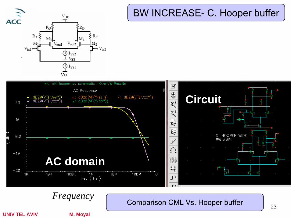
UNIV TEL AVIV M. Moyal23
BW INCREASE- C. Hooper buffer
Frequency
AC domain
Circuit
Comparison CML Vs. Hooper buffer
UNIV TEL AVIV M. Moyal24
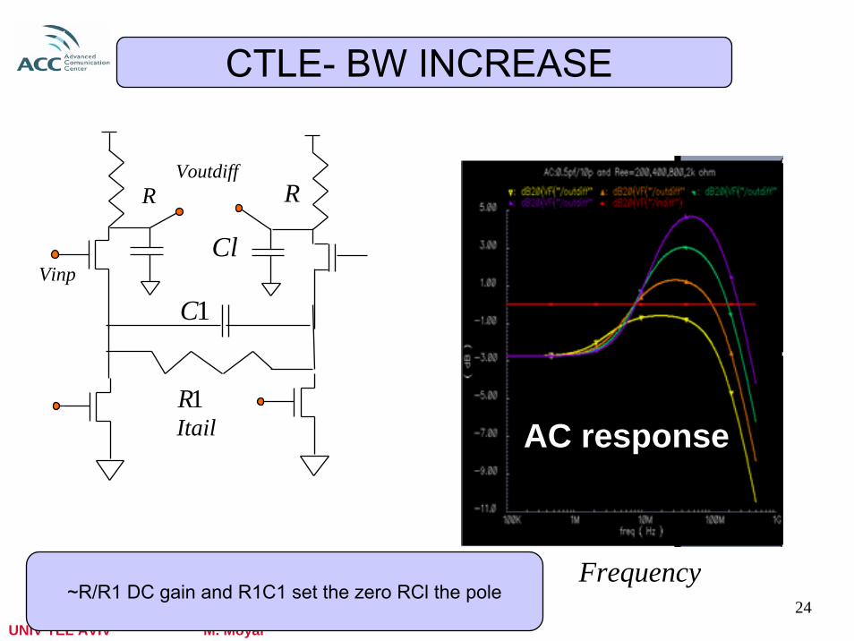
CTLE- BW INCREASE
R R
1CVinp
Itail
Voutdiff
Cl
1R
Frequency
AC response
~R/R1 DC gain and R1C1 set the zero RCl the pole
UNIV TEL AVIV M. Moyal25
At last: Even the faster known digital element the inverter can have
higher BW with some thoughts..

UNIV TEL AVIV M. Moyal26
High BW INVERTER High BW INVERTER
different feed backdifferent feed back
Frequency
time response
AC domain
Frequency
f/bf/b

UNIV TEL AVIV M. Moyal27
BW INCREASE“forget the BW do it another way?”
Digital-Half rates and..
DATA CONVERTERInterleaved with slow elements
6) “RF” ADCs for 10GS/s

UNIV TEL AVIV M. Moyal28
Even f/2Even f/2
Q
CKo
Q
CK
D
Odd f/2Odd f/2
CK
CKe
CKe CKe
D
muxmux
Cut rate by 2 – parallel data…parallel CPUs..

UNIV TEL AVIV M. Moyal29
““SlowSlow”” ADCs can be put in parallelADCs can be put in parallel
ADC1
ADC1
ADC1
ADC1
ADC1
ADC1
Vin(t)
fck1
delta=1.25ns
Vo(NT)
Analog S/H & Analog S/H & DemuxDemux Dig Dig MuxMux
fck2
Time interleavedTime interleaved

UNIV TEL AVIV M. Moyal30
..Recent advances in ADCs..Recent advances in ADCs
But we need lots of ADCs But we need lots of ADCs ––Power could kill the idea..Power could kill the idea..
So lets look at old ADC type....So lets look at old ADC type....

UNIV TEL AVIV M. Moyal31
SAR ADCs FOM HISTORY
0
0.05
0.1
0.15
0.2
2005 2006 2007 2008 2009Year
FOM
(pJ/
conv
)Is the SAR Is the SAR ““coming backcoming back”” ??
NbitteSamplingRaPower
2cision Energy/De
⋅=

UNIV TEL AVIV M. Moyal32
100ff100ff
1V1V00 00
50ff50ff00
00
25ff25ff
00
25ff25ff
VOUT(DAC)VOUT(DAC)
25)2550100/(100Vout(dac) +++∗= V1 VdacVout 2/1)( =
100ff100ff
1V1V00
50ff50ff00
00
25ff25ff
00
25ff25ff
VOUT(DAC)VOUT(DAC)
1V1V
25)255050/(100Vout(dac) +++∗= V1
operation..operation..

UNIV TEL AVIV M. Moyal33
Vin(t)
CompSAMPLE HOLD DIGITAL
Vo(nT)
offset DACoffset DAC
Lin DACLin DAC 10b DAC10b DAC
Gain DACGain DAC
ADC slice – lots of calibrations…

UNIV TEL AVIV M. Moyal34
תודה על ההקשבהתודה על ההקשבהThank youThank you