hardware implementation of cryptosystem by …€¦ · hardware implementation of cryptosystem by...
TRANSCRIPT
HARDWARE IMPLEMENTATION OF CRYPTOSYSTEM BY AES
ALGORITHM USING FPGA
Prachi Vijay Bhalerao Rahul D.Ghongde
ME IInd
Year Extc, ., P.R.Pote (Patil), C.O.E.M.,
P.R.Pote (Patil), C.O.E.M SGBAU University.
SGBAU University.
Abstract: Advanced Encryption Standard (AES) is an approved cryptographic Algorithm that can be
used to protect electronic data. The Advanced Encryption Standard can be programmed in software or
built with hardware. However Field Programmable Gate Arrays (FPGAS) offer a quicker, more
customizable solution.It is shown, how a modified structure in these Hardware devices results in
significant improvement of the design efficiency. The conventional scheme of AES is vulnerable for
cryptanalysis. This consumes a lot of Memory for the storage of look up table. Thus it is essential to
generate S-Bytes at run time. It is beneficial if the S-byte generated during run time varies with the
input key. Another weakness of AES is that it works with a single key. In this paper, a new scheme of
AES involving generation of Key based S-Boxes and dual key AES is proposed. This overcomes the
vulnerability of static S-Boxes and also single key encryption scheme.
Keywords: Cryptography, AES, FPGA, Static S-Box, Look up tables etc.
1.Introduction:
In these days use of digital data
exchange is increasing day by day in every
field. Information security plays very
important role in storing and transmitting the
data. When we transmit a multimedia data
such as audio, video, images etc. over the
network, cryptography provides security. As
we deal with Cryptography and Networking,
the main aim is to achieve the security of the
data. Hence, this paper presents “An
Equivalent Security in Cryptosystem by
Advance Encryption Standard Using FPGA”.
Advanced Encryption Standard (AES) is an
approved cryptographic Algorithm that can be
used to protect electronic data. AES is a
symmetrical algorithm of encoding intended to
replace DES which had already shown certain
faults of safety in the data Protection. The
Advanced Encryption Standard can be
programmed in software or built with
hardware. However Field Programmable Gate
Arrays (FPGAs) offer a quicker, more
customizable solution, hence we used the
FPGA as for implementation purpose. We
show how a modified structure in these
Hardware devices results in significant
improvement of the design efficiency. We
move on to discuss about the recent
modifications that have been done on the AES
scheme and their weaknesses.
AES consists of 128 block length of
bits and supports 128, 192 and 256 key length
bits. The 128 bits are organized Into state
matrix which is of the size of 4×4. This
algorithm starts with initial transformation of
state matrix Followed by nine iteration of
rounds. A round consists of four
transformations: Byte Substitution (subbytes),
Row Shifting (shiftrows), Mixing of columns
(mixcolumns) and followed by addition of
Round Key called (addroundkey). From each
round, a round key is generated from the
original key through key scheduling Process.
The last round consists of subbytes, shiftrows
and addroundkey transformation. Subbytes
Transformation is implemented using S-
Box.The S-Box is One of the most time
consuming process because it is required in
every round.
International Journal of Scientific & Engineering Research, Volume 7, Issue 2, February-2016 ISSN 2229-5518 606
IJSER © 2016 http://www.ijser.org
IJSER
Conventional Advanced encryption
standard
AES is based on rijndael algorithm
which is a symmetric block cipher that
processes fixed data of 128-bit blocks. It
supports key sizes of 128, 192 and 256 bits
and consists of 10, 12 or 14 iteration rounds,
respectively. In this paper we will focus on the
128-bit version with 10 rounds. Each round
mixes the data with a round key, which is
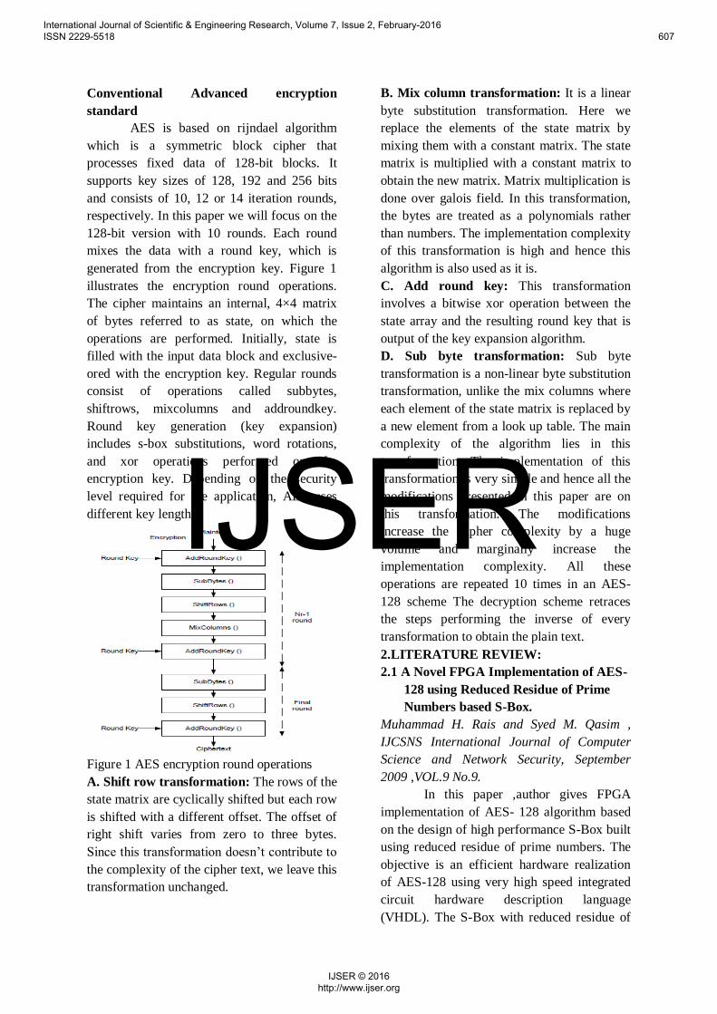
generated from the encryption key. Figure 1
illustrates the encryption round operations.
The cipher maintains an internal, 4×4 matrix
of bytes referred to as state, on which the
operations are performed. Initially, state is
filled with the input data block and exclusive-
ored with the encryption key. Regular rounds
consist of operations called subbytes,
shiftrows, mixcolumns and addroundkey.
Round key generation (key expansion)
includes s-box substitutions, word rotations,
and xor operations performed on the
encryption key. Depending on the security
level required for the application, AES uses
different key lengths.
Figure 1 AES encryption round operations
A. Shift row transformation: The rows of the
state matrix are cyclically shifted but each row
is shifted with a different offset. The offset of
right shift varies from zero to three bytes.
Since this transformation doesn’t contribute to
the complexity of the cipher text, we leave this
transformation unchanged.
B. Mix column transformation: It is a linear
byte substitution transformation. Here we
replace the elements of the state matrix by
mixing them with a constant matrix. The state
matrix is multiplied with a constant matrix to
obtain the new matrix. Matrix multiplication is
done over galois field. In this transformation,
the bytes are treated as a polynomials rather
than numbers. The implementation complexity
of this transformation is high and hence this
algorithm is also used as it is.
C. Add round key: This transformation
involves a bitwise xor operation between the
state array and the resulting round key that is
output of the key expansion algorithm.
D. Sub byte transformation: Sub byte
transformation is a non-linear byte substitution
transformation, unlike the mix columns where
each element of the state matrix is replaced by
a new element from a look up table. The main
complexity of the algorithm lies in this
transformation. The implementation of this
transformation is very simple and hence all the
modifications presented in this paper are on
this transformation. The modifications
increase the Cipher complexity by a huge
volume and marginally increase the
implementation complexity. All these
operations are repeated 10 times in an AES-
128 scheme The decryption scheme retraces
the steps performing the inverse of every
transformation to obtain the plain text.
2.LITERATURE REVIEW:
2.1 A Novel FPGA Implementation of AES-
128 using Reduced Residue of Prime
Numbers based S-Box.
Muhammad H. Rais and Syed M. Qasim ,
IJCSNS International Journal of Computer
Science and Network Security, September
2009 ,VOL.9 No.9.
In this paper ,author gives FPGA
implementation of AES- 128 algorithm based
on the design of high performance S-Box built
using reduced residue of prime numbers. The
objective is an efficient hardware realization
of AES-128 using very high speed integrated
circuit hardware description language
(VHDL). The S-Box with reduced residue of
International Journal of Scientific & Engineering Research, Volume 7, Issue 2, February-2016 ISSN 2229-5518 607
IJSER © 2016 http://www.ijser.org
IJSER
prime number adds more confusion to the
entire process of AES algorithm and makes it
more complex and provides further resistance
against attacks. The target hardware used in
this paper is state-of-the-art FPGA from
Xilinx. The proposed design achieves a
throughput of 3.09 Gbps using only 1745
slices. Author presented FPGA
implementation of AES utilizing high
performance S-Box which uses reduced
residue of prime numbers. The objective is to
use a S-Box based on LUT whose entries are
set of residue of prime number. The S-Box
with reduced residue of prime number adds
more confusion to the entire process of AES
algorithm and makes it more complex and
provides further resistance against attacks.
2.2 Area Optimized and Pipelined FPGA
Implementation of AES Encryption &
Decryption
Mg Suresh and Dr.Nataraj.K.R, International
Journal of Computational Engineering
Research (ijceronline.com) November 2012
Vol. 2 Issue. 7.
This paper talks of AES 128 bit block
and 128 bit cipher key and is implemented on
Spartan 3 FPGA using VHDL as the
programing language. The mode of data
transmission is modified in this design so that
the chip size can be reduced. The 128-bit
plaintext and the 128- bit initial key, as well as
the 128-bit output of cipher text, are all
divided into four 32-bit consecutive units
respectively controlled by the clock. This
system aims at reduced hardware structure and
high throughput. Author concluded that the
concept of Pipelined AES architecture can be
practically implemented. It has been observed
that the implementation of AES Encryption on
the FPGA is successful and several data input.
The cipher key can be changed with respect to
the user requirements. The result shows that
the design with the pipelining technology and
special data transmission mode can optimize
the chip area effectively.While implementing
the AES Algorithm, the critical aspect was the
area utilization. Which was done using
implementation of functions for different sub
modules in the algorithm the work has
approximately reduced around 10% utilization
on chip as compared to basic available
modules.
2.3 Design and Implementation of AES
Security Algorithm using FPGA
Adnan Mohsin Abdulazeez, International
Journal of Scientific & Engineering Research,
September-2013 Volume 4, Issue 9.
In this paper, author gives two
architectures, one for AES Encryption process,
and the other for AES Decryption process.
Both architectures are based on an iterative
structure and modifications such as merging
transformation (SubByte and ShiftRow in
Encryption process, and Inverse SubByte and
Inverse ShiftRow in Decryption process),
Look Up tables for decryption, generating
keys, and optimization of each clock cycle to
incorporate maximum number of operations to
improve the throughput and reducing hardware
resources. The design has been described by
VHDL and simulated by using Xilinx ISE
9.2i.The architectures have been implemented
on reconfigurable platforms FPGAs.
Accomplishment when implemented on
Xilinx_Virtex4 which confirms that the
proposed architectures have minimum
hardware resource, where only 9% of the chip
resources are used for AES Encryption design
with realizable operating clock frequency of
382.988MHz, and only 9% of the chip
resources are used for AES Decryption design
with realizable operating clock frequency of
382.988MHz. The Keys have been generated
for all rounds before the data goes through the
rounds. The SubShiftByte entity merges both
the ShiftRow and Subbyte transformation and
InvSub-Shiftbyte merges both InvShift and
InvSubByte entities. The Sbox and InvSbox
array's elements have been stored in the
memory in order to be ready for substitute
byte.
2.4 Implementation and Design of AES S-
Box on FPGA
Chandrasekhar Savalam & Prasanti Korapati,
International Journal of Research in
International Journal of Scientific & Engineering Research, Volume 7, Issue 2, February-2016 ISSN 2229-5518 608
IJSER © 2016 http://www.ijser.org
IJSER

Engineering and Science (IJRES) ISSN
(Online): 2320-9364,www.ijres.org, Jan.
2015, Volume 3 Issue 1.
The author said that AES can be
programmed in software or built with pure
hardware. However, FPGAs offer a quicker,
more customizable solution. This research
investigates the AES algorithm with regard to
FPGA and VHDL. Xilinx Design Suite 14.5
software is used for simulation and
optimization of the synthesizable VHDL code.
All the transformations of both Encryptions is
simulated using an iterative design approach in
order to minimize the hardware consumption.
Virtex 6 Family devices are utilized for
hardware evaluation.The hardware complexity
in AES is dominated by S-box which is
considered as one of the most complicated and
costly part of the system because it is the only
non-linear structure.The design reduces the
overall delay and efficiently for applications
with high-speed performance. This approach is
suitable for FPGA implementation in term of
gate area. The hardware, total area and delay
are presented. The author proposed S-Box
gives another option for hardware
implementation other than composite field to
represent Sub byte transformation. It reduces
the complexities of hardware by avoiding the
use of multiplicative inverse in Galois field.
PROPOSED SYSTEM:
It is mentioned that there are two ways
of generation of S-Bytes.
1. Look up tables.
2. Dynamic generation of S-Bytes.
The first method consumes a lot of memory in
order to store the look up table for each byte.
The second method consumes significantly
less area but marginally adds to the
performance overhead. In this paper we
propose a slightly modified version of the AES
algorithm and the architecture used for the
efficient implementation of the algorithm. The
proposed algorithm involves the generation of
key based S-Bytes. The two keys used for the
algorithm are called User Key and System
Key. System Key is generated within the
system and User key is input to the system by
the user.
The algorithm used for AES is as shown
below:
Fig 2. Block Diagram of Dual Key Based AES
The user inputs an 8-bit value called
SEED for the generation of System Key. 16
pre-defined keys are stored in the form of a
look up table. A 4 bit offset is generated from
the SEED to select one of the keys as System
Key. But the pre-defined keys that are stored
are of 120 bit length. The generation of the
128 bit System Key happens as follows:
1. A 4 bit offset is generated by bitwise XOR
of higher nibble and the lower nibble.
2. The 120 bit key corresponding to the
location of the offset value is selected.
3. Append the value of the SEED to the 120
bit Key to obtain a 128 bit SYSTEM KEY.
The System Key is used for the generation of
S-Byte and the user key is used for the ADD
ROUND KEY transformation. The S-Byte
transformation used for ADD ROUND KEY is
the conventional static S-Byte. This is done in
order to avoid complexity during the
decryption process. The System key for the
next round will be obtained by bitwise XOR of
the Next Round Key with the System Key.
This algorithm removes the computational
overheads that do not add to the complexity of
the cipher and adds simple transformations
that add to the complexity of the cipher.
3. CONCLUSION
Many of modification have been done
on AES encryption. Among the ones, the
complexity of the algorithm lies in the
generation of S-Boxes. This also makes the
International Journal of Scientific & Engineering Research, Volume 7, Issue 2, February-2016 ISSN 2229-5518 609
IJSER © 2016 http://www.ijser.org
IJSER

hardware implementation of the algorithm
very complex. Also the level of security
provided is a tradeoff with the amount of
resources consumed. This paper gives a brief
overview about the conventional AES
encryption and also about its vulnerabilities.
From these review the algorithm was
simulated for a clock frequency of 1GHz and
the output was obtained in 40 clock cycles.
REFERENCES:
[1] “FPGA Implementation of Dual Key Based AES Encryption with
Key Based S Box Gene -ration” Abhiram L S, Sriroop B K, 978-9-
3805-4416- 2015 IEEE [2] “A Novel FPGA Implementation of
AES-128 using Reduced Residue of
Prime Numbers based S-Box”
Muhammad H. Rais and Syed M.
Qasim ,IJCSNS International
Journal of Computer Science and
Network Security, September
2009,VOL.9No 9.
[3] “Area Optimized and Pipelined FP -
GA Implementation of AES
Encryption & Decryption”Mg
Suresh and
Dr.Nataraj.K.R,International
Journal of Computational
Engineering Research
(ijceronline.com) November
2012,Vol. 2 Issue. 7.
[4] “Design and Implementation of AES
Security Algorithm using FPGA”
Adnan Mohsin Abdulazeez, Inter-
national Journal of Scientific & Engg.
Research, September-2013 Vol 4, Issue
9.
[5] “Implementation and Design of AES
S- Box on FPGA” Chandrasekhar
Savalam & Prasanti
Korapati, International Journal of
Research in Engineering and Science
(IJRES) ISSN (Online): 2320- 9364,
www.ijres.org, Jan. 2015,Vol 3 Issue
1.
International Journal of Scientific & Engineering Research, Volume 7, Issue 2, February-2016 ISSN 2229-5518 610
IJSER © 2016 http://www.ijser.org
IJSER