guoyong shi · sheldon x.-d. tan esteban tlelo cuautle
TRANSCRIPT

Guoyong Shi · Sheldon X.-D. TanEsteban Tlelo Cuautle
Advanced Symbolic Analysis for VLSI SystemsMethods and Applications

Advanced Symbolic Analysis for VLSI Systems
Guoyong Shi • Sheldon X.-D. TanEsteban Tlelo Cuautle
Advanced Symbolic Analysisfor VLSI Systems
Methods and Applications
123

Guoyong ShiSchool of MicroelectronicsShanghai Jiao Tong UniversityShanghaiChina
Sheldon X.-D. TanDepartment of Electrical EngineeringUniversity of CaliforniaRiverside, CAUSA
Esteban Tlelo CuautleINAOETonantzintla, PueblaMexico
ISBN 978-1-4939-1102-8 ISBN 978-1-4939-1103-5 (eBook)DOI 10.1007/978-1-4939-1103-5Springer New York Heidelberg Dordrecht London
Library of Congress Control Number: 2014941630
� Springer Science+Business Media New York 2014This work is subject to copyright. All rights are reserved by the Publisher, whether the whole or part ofthe material is concerned, specifically the rights of translation, reprinting, reuse of illustrations,recitation, broadcasting, reproduction on microfilms or in any other physical way, and transmission orinformation storage and retrieval, electronic adaptation, computer software, or by similar or dissimilarmethodology now known or hereafter developed. Exempted from this legal reservation are briefexcerpts in connection with reviews or scholarly analysis or material supplied specifically for thepurpose of being entered and executed on a computer system, for exclusive use by the purchaser of thework. Duplication of this publication or parts thereof is permitted only under the provisions ofthe Copyright Law of the Publisher’s location, in its current version, and permission for use mustalways be obtained from Springer. Permissions for use may be obtained through RightsLink at theCopyright Clearance Center. Violations are liable to prosecution under the respective Copyright Law.The use of general descriptive names, registered names, trademarks, service marks, etc. in thispublication does not imply, even in the absence of a specific statement, that such names are exemptfrom the relevant protective laws and regulations and therefore free for general use.While the advice and information in this book are believed to be true and accurate at the date ofpublication, neither the authors nor the editors nor the publisher can accept any legal responsibility forany errors or omissions that may be made. The publisher makes no warranty, express or implied, withrespect to the material contained herein.
Printed on acid-free paper
Springer is part of Springer Science+Business Media (www.springer.com)

To our families

Preface
Symbolic analysis is an intriguing topic for VLSI design. Traditional symbolicanalysis is typically concerned with deriving exact or approximate analyticexpressions of analog circuit performance in terms of circuit parameters. Suchsymbolic expressions give clear relationships between circuit performances andtunable parameters, which in turn can be very helpful for design optimization.Instead of competing with numerical analysis tools like SPICE, symbolic analysistools can provide complementary information for circuit designers.
Over the past two decades, symbolic analysis techniques have seen significantadvances. Definition and applications of symbolic analysis also become broader.Many advanced circuit analysis techniques such as moment-based techniques andmodel order reduction techniques can be viewed as special symbolic analysistechniques if the complex frequency variables are considered as symbols. One ofthe major advances in symbolic analysis achieved during this period is theintroduction of structural compact graph-based approaches to efficiently representthe generated symbolic terms, which may suppress the exponential growth rate ofcomplexity with respect to the circuit sizes. Such compact graph-based approachesenable exact symbolic analysis of practical analog modules, which would not bepossible by using any traditional symbolic methods. The following up graph-basedhierarchical approaches can in principle analyze analog circuits of any size.
Another recent advance is successful applications of symbolic analysis tech-niques to tasks requiring many repeated computations such as Monte Carlo-basedstatistical circuit verification and optimization in the presence of manufacturingprocess variations. In such applications, symbolic methods can provide superioradvantage over traditional numerical analysis. Symbolic analysis-based methodscan mitigate the long-standing low-efficiency issues for computing the rare events(high sigma) in Monte Carlo analysis and are scalable for high-dimensional, large-variation problems suffered by some other statistical methods.
In spite of many recent advances in this area, no single monograph has beenwritten to systematically present the comprehensive symbolic analysis techniquesdeveloped recently. This book is intended to fill this gap by providing a detailedtreatment from the prospectives of theory, algorithm development, implementa-tion, and applications. This book starts from the introduction of basic symbolicanalysis concepts and graph-based construction techniques. It then covers algo-rithmic formulations and computer implementations with emphasis on memory
vii

management and complexity issues. It finally proceeds to several importantapplications related to timing analysis, statistical modeling, sensitivity analysis aswell as parallel computation. The whole book is organized into three relativelyindependent parts: the fundamentals, the implementation methods, and theapplications for VLSI design.
Part I presents motivation for symbolic analysis and an overview on the clas-sical symbolic analysis methods. Emphasis is made on the principle of moderncompact graph-based symbolic analysis, its advantages, and its impact onapplications. Since binary decision diagrams (BDDs) are the key data structureused by the new generation of symbolic methods introduced in this book,preliminaries on the concept of BDD are provided as well to make this book self-contained. This part of the review goes through the history and roles of BDD inlogic synthesis and verification. Then it elaborates on the recent extensions tosymbolic analog integrated circuit analysis. Some BDD-specific implementationstrategies such as zero suppression, variable ordering, and canonical reduction areexplained in detail as well.
Part II focuses on the computer implementation of advanced symbolic analysistechniques. The presentation follows a historical development. First, the details forthe construction of determinant decision diagrams (DDDs) are presented.The DDD symbolic method was the first matrix-based method formulated in BDDfor compact term generation. Second, a recently developed DDD implementationvariant is presented, which has the feature of easily understood implementationdetails. Based on this implementation, a theoretical result on the DDD computa-tional complexity is derived, which indicates a fact that the efficiency of DDDessentially comes from a suppression of the exponential complexity growth rate.Third, we proceed to the introduction of a more recently proposed symbolicalgorithm called Graph-Pair Decision Diagram (GPDD). The construction ofGPDD is based on an extension of the classical two-graph method which has theguarantee of cancellation-free term generation. In the last section of this part, weintroduce several recently developed hierarchical analysis strategies for largeranalog modules. These methods combine the specific advantages of DDD andGPDD by considering whether a formulated hierarchical strategy is suitable forcircuit partitioning and multilevel assembling.
Part III presents several parametric modeling and analysis methods based onadvanced symbolic techniques. First, a novel symbolic moment computationstrategy is developed, in which the computation of moments of mesh-structuredinterconnect networks is performed by creating BDD-based representation of amesh decomposition process. The decomposition employs the branch tearingtechnique known in the literature without going through any matrix formulation.This method is then applied to statistical timing and cross talk analysis of meshnetworks. Second, a DDD-based symbolic analysis technique for performancebound estimation of analog circuits subject to process variations is presented. It isshown that symbolic expressions can be used to find the min/max performancebounds much more efficiently than traditional numerical methods. Third, weintroduce a novel GPU accelerated parallel Monte Carlo statistical analysis based
viii Preface

on DDD structures. We show that the localized data dependency among the DDDnodes in a DDD graph is very simple and hence highly amenable to GPU-basedfine-grained parallel computing.
Future errata and update about this book can be found at http://www.ee.ucr.edu/*stan/project/books/book12_symblic_ana.htm.
Guoyong ShiSheldon X.-D. Tan
Esteban Tlelo Cuautle
Preface ix
Acknowledgments
The authors would like first to acknowledge Prof. C.-J. Richard Shi of Universityof Washington for inspiring many of the original ideas presented in this book.In addition, the authors are grateful to the research funding sponsors for theirfinancial supports, and to many students and visiting scholars for their researchcontributions.
Sheldon X.-D. Tan thanks both National Science Foundation and University ofCalifornia at Riverside for their financial supports for this book. SheldonX.-D. Tan highly appreciates the consistent supports of Dr. Sankar Basu ofNational Science Foundation over the past decade. Without these supports, manyof the works would not be possible. Specifically, Sheldon X-.D. Tan acknowledgesthe following grants: NSF grant under No. CCF-1116882, No. CCF-1017090,OISE-1130402, and UC MEXUS-CONACYT Collaborative Research Grant underNo. CN-11-575, which was done in collaboration with Esteban Tlelo Cuautle.He also thanks the supports of UC Regent’s Committee on Research (COR)Fellowship. He is grateful to the following people for their contribution to thisbook: Dr. Xuexin Liu and Dr. Zhigang Hao for some of their research workspresented in this book; Dr. Haibao Chen, who is a Postdoc at MSLAB forproofreading the book; Ms. Yan Zhu, who is a Ph.D. student at MSLAB, forfine-tuning and proofreading this book.
Guoyong Shi is grateful to the sponsorship from the Natural Science Founda-tion of China (NSFC), which has provided continuing research support since 2006.He would like to acknowledge the following NSFC grants he has received so far,No. 60572028 in 2006, No. 60876089 from 2009 to 2011, and No. 61176129 from2012 to 2015. He is also indebted to many graduate students who worked in theMixed-Signal Design Automation (MSDA) Laboratory of the School of Micro-electronics in Shanghai Jiao Tong University. Some of the results reported in thisbook come from their research contributions.
Esteban Tlelo Cuautle thanks CONACyT at Mexico for the partial supportunder project 131839.
Last but not the least, Sheldon X.-D. Tan thanks his wife, Yan Ye, his threedaughters for understanding and supports during many hours it took to write thisbook. Guoyong Shi thanks his family for patience and support while we waswriting part of this monograph. Esteban Tlelo Cuautle expresses his gratitude tohis family.
xi

Contents
Part I Fundamentals
1 Introduction . . . . . . . . . . . . . . . . . . . . . . . . . . . . . . . . . . . . . . . . 31 Book Outline . . . . . . . . . . . . . . . . . . . . . . . . . . . . . . . . . . . . . 3
1.1 Fundamental of Symbolic Analysis . . . . . . . . . . . . . . . . . . 31.2 Basic Techniques for Symbolic Analysis . . . . . . . . . . . . . . 41.3 Applications of Symbolic Analysis . . . . . . . . . . . . . . . . . . 5
2 Summary . . . . . . . . . . . . . . . . . . . . . . . . . . . . . . . . . . . . . . . . 6
2 Symbolic Analysis Techniques in a Nutshell. . . . . . . . . . . . . . . . . 71 Introduction . . . . . . . . . . . . . . . . . . . . . . . . . . . . . . . . . . . . . . 7
1.1 Symbolic Analysis Problem . . . . . . . . . . . . . . . . . . . . . . . 82 Symbolic Analysis for Analog Circuits . . . . . . . . . . . . . . . . . . . 9
2.1 Behavioral Modeling for Active Devices . . . . . . . . . . . . . . 92.2 Circuit Formulation . . . . . . . . . . . . . . . . . . . . . . . . . . . . . 102.3 Determinant Decision Diagrams . . . . . . . . . . . . . . . . . . . . 122.4 Two-Graph Based Symbolic Analysis . . . . . . . . . . . . . . . . 122.5 Noise and Distortion Analysis . . . . . . . . . . . . . . . . . . . . . 132.6 Symbolic Approximation Approaches . . . . . . . . . . . . . . . . 142.7 Application to Circuit Synthesis . . . . . . . . . . . . . . . . . . . . 142.8 Miscellaneous Applications . . . . . . . . . . . . . . . . . . . . . . . 15
3 Symbolic Analysis and Model Order Reduction . . . . . . . . . . . . . 153.1 Krylov Subspace Based Reduction . . . . . . . . . . . . . . . . . . 153.2 Truncated Balanced Realization Based Reduction . . . . . . . . 163.3 Parameterized and Variational Reduction . . . . . . . . . . . . . . 17
4 Mathematical Concepts and Notation . . . . . . . . . . . . . . . . . . . . 184.1 Matrix, Determinant, and Cofactor . . . . . . . . . . . . . . . . . . 184.2 Cramer’s Rule . . . . . . . . . . . . . . . . . . . . . . . . . . . . . . . . 19
5 Summary . . . . . . . . . . . . . . . . . . . . . . . . . . . . . . . . . . . . . . . . 20
3 Binary Decision Diagram for Symbolic Analysis . . . . . . . . . . . . . 211 Basic Concepts and Notation . . . . . . . . . . . . . . . . . . . . . . . . . . 212 Canonicity of BDD . . . . . . . . . . . . . . . . . . . . . . . . . . . . . . . . . 243 Logic Operations on BDDs . . . . . . . . . . . . . . . . . . . . . . . . . . . 28
xiii

4 BDD for Algebraic Symbolic Analysis . . . . . . . . . . . . . . . . . . . 304.1 BDD for Determinant Expansion . . . . . . . . . . . . . . . . . . . 304.2 BDD for Spanning Tree Enumeration . . . . . . . . . . . . . . . . 324.3 Benefits of Using BDD for Symbolic Analysis . . . . . . . . . . 36
5 BDD Implementation . . . . . . . . . . . . . . . . . . . . . . . . . . . . . . . 386 Summary . . . . . . . . . . . . . . . . . . . . . . . . . . . . . . . . . . . . . . . . 42
Part II Methods
4 Determinant Decision Diagrams . . . . . . . . . . . . . . . . . . . . . . . . . 451 Introduction . . . . . . . . . . . . . . . . . . . . . . . . . . . . . . . . . . . . . . 452 Exact Symbolic Analysis by Determinant Decision Diagrams . . . 453 DDD Representation of Symbolic Determinant. . . . . . . . . . . . . . 464 Manipulation of Determinant Decision Diagrams . . . . . . . . . . . . 50
4.1 Implementation of Basic Operations . . . . . . . . . . . . . . . . . 515 DDD Construction by Logic Operations . . . . . . . . . . . . . . . . . . 53
5.1 Terms-Detecting Logic for a Determinant . . . . . . . . . . . . . 535.2 Logic Operation Based DDD Construction Algorithm . . . . . 545.3 Logic Synthesis Perspective . . . . . . . . . . . . . . . . . . . . . . . 565.4 Time Complexity Analysis . . . . . . . . . . . . . . . . . . . . . . . . 57
6 s-Expanded Determinant Decision Diagrams . . . . . . . . . . . . . . . 576.1 s-Expanded Symbolic Representation . . . . . . . . . . . . . . . . 586.2 Construction of s-Expanded DDDs . . . . . . . . . . . . . . . . . . 63
7 DDD-Based Symbolic Approximation . . . . . . . . . . . . . . . . . . . . 647.1 Finding Dominant Terms by Incremental k-Shortest
Path Algorithm . . . . . . . . . . . . . . . . . . . . . . . . . . . . . . . . 658 Summary . . . . . . . . . . . . . . . . . . . . . . . . . . . . . . . . . . . . . . . . 70
5 DDD Implementation . . . . . . . . . . . . . . . . . . . . . . . . . . . . . . . . . 711 Introduction . . . . . . . . . . . . . . . . . . . . . . . . . . . . . . . . . . . . . . 712 Early Versions of DDD Implementation . . . . . . . . . . . . . . . . . . 723 Minor Hash Function . . . . . . . . . . . . . . . . . . . . . . . . . . . . . . . 744 Layered Expansion of Determinant . . . . . . . . . . . . . . . . . . . . . . 755 LED Implementation. . . . . . . . . . . . . . . . . . . . . . . . . . . . . . . . 78
5.1 Expansion Order in LED . . . . . . . . . . . . . . . . . . . . . . . . . 785.2 Hash in LED . . . . . . . . . . . . . . . . . . . . . . . . . . . . . . . . . 805.3 The LED Construction Procedure . . . . . . . . . . . . . . . . . . . 82
6 Examples . . . . . . . . . . . . . . . . . . . . . . . . . . . . . . . . . . . . . . . . 826.1 Test on Full Matrices . . . . . . . . . . . . . . . . . . . . . . . . . . . 836.2 Test on Analog Circuits . . . . . . . . . . . . . . . . . . . . . . . . . . 85
xiv Contents

7 Complexity Analysis . . . . . . . . . . . . . . . . . . . . . . . . . . . . . . . . 877.1 DDD Optimality . . . . . . . . . . . . . . . . . . . . . . . . . . . . . . . 877.2 Remarks on the DDD Optimal Order . . . . . . . . . . . . . . . . 92
8 Summary . . . . . . . . . . . . . . . . . . . . . . . . . . . . . . . . . . . . . . . . 94
6 Generalized Two-Graph Theory . . . . . . . . . . . . . . . . . . . . . . . . . 951 Introduction . . . . . . . . . . . . . . . . . . . . . . . . . . . . . . . . . . . . . . 952 Two-graph Method for Dependent Sources . . . . . . . . . . . . . . . . 973 Extension to Mirror Elements. . . . . . . . . . . . . . . . . . . . . . . . . . 104
3.1 Definition of Mirror Elements . . . . . . . . . . . . . . . . . . . . . 1053.2 Bidirectional Edges . . . . . . . . . . . . . . . . . . . . . . . . . . . . . 1063.3 Parallel Connection of G . . . . . . . . . . . . . . . . . . . . . . . . . 108
4 Sign of Two-tree . . . . . . . . . . . . . . . . . . . . . . . . . . . . . . . . . . 1095 Summary of Generalized Two-graph Rules . . . . . . . . . . . . . . . . 1116 Compact Two-graph As Intermediate Form . . . . . . . . . . . . . . . . 114
6.1 Admissible Two-tree Enumeration . . . . . . . . . . . . . . . . . . 1156.2 Nodal Admittance Matrix Formulation . . . . . . . . . . . . . . . 115
7 Examples . . . . . . . . . . . . . . . . . . . . . . . . . . . . . . . . . . . . . . . . 1198 Summary . . . . . . . . . . . . . . . . . . . . . . . . . . . . . . . . . . . . . . . . 124
7 Graph-Pair Decision Diagram . . . . . . . . . . . . . . . . . . . . . . . . . . . 1251 Introduction . . . . . . . . . . . . . . . . . . . . . . . . . . . . . . . . . . . . . . 1252 Definitions and Main Result. . . . . . . . . . . . . . . . . . . . . . . . . . . 1263 Implicit Enumeration by BDD . . . . . . . . . . . . . . . . . . . . . . . . . 128
3.1 Edge-Pair Operations. . . . . . . . . . . . . . . . . . . . . . . . . . . . 1303.2 Construction of GPDD. . . . . . . . . . . . . . . . . . . . . . . . . . . 1303.3 Symbolic Expressions in GPDD . . . . . . . . . . . . . . . . . . . . 133
4 GPDD Implementation . . . . . . . . . . . . . . . . . . . . . . . . . . . . . . 1364.1 Graph Hash . . . . . . . . . . . . . . . . . . . . . . . . . . . . . . . . . . 1364.2 Main Routines . . . . . . . . . . . . . . . . . . . . . . . . . . . . . . . . 1374.3 Sign Determination . . . . . . . . . . . . . . . . . . . . . . . . . . . . . 1394.4 Canonical GPDD . . . . . . . . . . . . . . . . . . . . . . . . . . . . . . 142
5 GPDD Performance Evaluation . . . . . . . . . . . . . . . . . . . . . . . . 1426 A Discussion on Cancellation-Free . . . . . . . . . . . . . . . . . . . . . . 1477 Summary . . . . . . . . . . . . . . . . . . . . . . . . . . . . . . . . . . . . . . . . 149
8 Hierarchical Analysis Methods . . . . . . . . . . . . . . . . . . . . . . . . . . 1511 Introduction . . . . . . . . . . . . . . . . . . . . . . . . . . . . . . . . . . . . . . 1512 Existing Hierarchical Methods . . . . . . . . . . . . . . . . . . . . . . . . . 152
2.1 Symbolic Analysis in SOE . . . . . . . . . . . . . . . . . . . . . . . . 1542.2 Gaussian Elimination Method . . . . . . . . . . . . . . . . . . . . . . 1562.3 Schur Decomposition with DDD. . . . . . . . . . . . . . . . . . . . 157
Contents xv

3 Symbolic Stamp Construction . . . . . . . . . . . . . . . . . . . . . . . . . 1603.1 Symbolic Stamp by Multiroot DDD . . . . . . . . . . . . . . . . . 1613.2 Symbolic Stamp by Multiroot GPDD . . . . . . . . . . . . . . . . 161
4 Reduction Rule for Multiport Element. . . . . . . . . . . . . . . . . . . . 1645 Hierarchical BDD Strategies . . . . . . . . . . . . . . . . . . . . . . . . . . 166
5.1 GPDD+DDD Hierarchy. . . . . . . . . . . . . . . . . . . . . . . . . . 1675.2 Hierarchical GPDD Analysis . . . . . . . . . . . . . . . . . . . . . . 169
6 Examples . . . . . . . . . . . . . . . . . . . . . . . . . . . . . . . . . . . . . . . . 1706.1 Examples for the GPDD+DDD Method . . . . . . . . . . . . . . 1726.2 Examples for the HierGPDD Method . . . . . . . . . . . . . . . . 173
7 Summary . . . . . . . . . . . . . . . . . . . . . . . . . . . . . . . . . . . . . . . . 176
9 Symbolic Nodal Analysis of Analog Circuits Using Nullors. . . . . . 1791 Introduction . . . . . . . . . . . . . . . . . . . . . . . . . . . . . . . . . . . . . . 1792 Modeling Active Devices Using Nullors . . . . . . . . . . . . . . . . . . 179
2.1 Nullor Concept . . . . . . . . . . . . . . . . . . . . . . . . . . . . . . . . 1802.2 Nullor Equivalent of the MOSFET . . . . . . . . . . . . . . . . . . 1812.3 Nullor Equivalents of Active Devices . . . . . . . . . . . . . . . . 1832.4 Nullor Equivalents of CMOS Amplifiers . . . . . . . . . . . . . . 184
3 Deriving Symbolic Expressions and SimplificationApproaches . . . . . . . . . . . . . . . . . . . . . . . . . . . . . . . . . . . . . . 1873.1 Symbolic Analysis Using Nullor-Equivalents
of Current-Mirrors. . . . . . . . . . . . . . . . . . . . . . . . . . . . . . 1893.2 Symbolic Behavioral Modeling for CMOS amplifiers . . . . . 1913.3 Solving the Symbolic NA Formulation
for Large Circuits . . . . . . . . . . . . . . . . . . . . . . . . . . . . . . 1943.4 Small-Signal Models and Nullor Equivalents
by Levels of Abstraction . . . . . . . . . . . . . . . . . . . . . . . . . 1954 Symbolic Sensitivity Analysis . . . . . . . . . . . . . . . . . . . . . . . . . 1965 Noise Analysis of Nullor Circuits . . . . . . . . . . . . . . . . . . . . . . . 2016 Summary . . . . . . . . . . . . . . . . . . . . . . . . . . . . . . . . . . . . . . . . 209
Part III Applications
10 Symbolic Moment Computation . . . . . . . . . . . . . . . . . . . . . . . . . 2131 Introduction . . . . . . . . . . . . . . . . . . . . . . . . . . . . . . . . . . . . . . 2132 Moment Computation by BDD. . . . . . . . . . . . . . . . . . . . . . . . . 216
2.1 Moment Computation for Tree Circuits . . . . . . . . . . . . . . . 2172.2 Moment Computation for Coupled Trees . . . . . . . . . . . . . . 222
3 Mesh Circuits with Multiple Sources. . . . . . . . . . . . . . . . . . . . . 2243.1 Kron’s Tearing and Mesh Decomposition . . . . . . . . . . . . . 2253.2 Moment Computation for Mesh Circuits . . . . . . . . . . . . . . 2273.3 High-Order Moments. . . . . . . . . . . . . . . . . . . . . . . . . . . . 229
xvi Contents

3.4 The SMC Algorithm . . . . . . . . . . . . . . . . . . . . . . . . . . . . 2313.5 Incremental Analysis . . . . . . . . . . . . . . . . . . . . . . . . . . . . 2313.6 Algorithm Complexity . . . . . . . . . . . . . . . . . . . . . . . . . . . 233
4 Symbolic Moment Sensitivity. . . . . . . . . . . . . . . . . . . . . . . . . . 2335 SMC Efficiency . . . . . . . . . . . . . . . . . . . . . . . . . . . . . . . . . . . 2356 Summary . . . . . . . . . . . . . . . . . . . . . . . . . . . . . . . . . . . . . . . . 237
11 Performance Bound Analysis of Analog CircuitsConsidering Process Variations . . . . . . . . . . . . . . . . . . . . . . . . . . 2391 Introduction . . . . . . . . . . . . . . . . . . . . . . . . . . . . . . . . . . . . . . 2392 Variational Transfer Functions Based on DDDs . . . . . . . . . . . . . 241
2.1 Variational Transfer Functions Dueto Process Variations . . . . . . . . . . . . . . . . . . . . . . . . . . . . 241
3 Computation of Frequency Domain Bounds . . . . . . . . . . . . . . . . 2424 Time Domain Bound Analysis Method . . . . . . . . . . . . . . . . . . . 246
4.1 Review of Transient Bound Analysis Drivenby Impulse Signals . . . . . . . . . . . . . . . . . . . . . . . . . . . . . 246
4.2 The General Signal Transient BoundAnalysis Method . . . . . . . . . . . . . . . . . . . . . . . . . . . . . . . 248
5 Direct Time-Domain Performance Bound Analysis . . . . . . . . . . . 2525.1 Symbolic Transient Analysis for Analog Circuits . . . . . . . . 2525.2 Variational Symbolic Closed-Form Expressions
for Transient States . . . . . . . . . . . . . . . . . . . . . . . . . . . . . 2555.3 Variational Bound Analysis in Time Domain . . . . . . . . . . . 255
6 Examples and Discussions . . . . . . . . . . . . . . . . . . . . . . . . . . . . 2566.1 Frequency Domain Response Bounds . . . . . . . . . . . . . . . . 2576.2 Time Domain Response Bounds . . . . . . . . . . . . . . . . . . . . 2616.3 Example and Discussions . . . . . . . . . . . . . . . . . . . . . . . . . 2626.4 An Interconnect RC Tree Circuit Example . . . . . . . . . . . . . 2646.5 An Opamp Circuit Example . . . . . . . . . . . . . . . . . . . . . . . 268
7 Summary . . . . . . . . . . . . . . . . . . . . . . . . . . . . . . . . . . . . . . . . 270
12 Statistical Parallel Monte-Carlo Analysis on GPUs . . . . . . . . . . . 2711 Introduction . . . . . . . . . . . . . . . . . . . . . . . . . . . . . . . . . . . . . . 2712 Review of GPU Architectures . . . . . . . . . . . . . . . . . . . . . . . . . 2723 The Graph-Based Parallel Statistical Analysis . . . . . . . . . . . . . . 273
3.1 The Overall Algorithm Flow . . . . . . . . . . . . . . . . . . . . . . 2743.2 The Continuous and Levelized DDD Structure . . . . . . . . . . 275
4 The Parallel GPU-Based Monte-Carlo Analysis Method . . . . . . . 2764.1 Random Number Assignment to MNA Elements
and DDD Nodes . . . . . . . . . . . . . . . . . . . . . . . . . . . . . . . 2764.2 Parallel Evaluation of DDDs . . . . . . . . . . . . . . . . . . . . . . 278
5 Examples . . . . . . . . . . . . . . . . . . . . . . . . . . . . . . . . . . . . . . . . 2796 Summary . . . . . . . . . . . . . . . . . . . . . . . . . . . . . . . . . . . . . . . . 282
Contents xvii

References . . . . . . . . . . . . . . . . . . . . . . . . . . . . . . . . . . . . . . . . . . . . 283
Index . . . . . . . . . . . . . . . . . . . . . . . . . . . . . . . . . . . . . . . . . . . . . . . . 297
xviii Contents

Part IFundamentals

Chapter 1Introduction
1 Book Outline
Symbolic analysis traditionally is referred to as a technique to generate analyticexpressions for circuit performances in terms of circuit component parameters andfrequency variables. Its study started in the 1960s, a decade earlier than the timenumerical circuit analysis techniques became popular. Although numerical analysistechniques have remained in the main-stream for circuit-level simulation, symbolicanalysis can serve as a good complement to numerical analysis. Recent advances insymbolic analysis, specially the compact graph-based symbolic analysis techniquescombined with hierarchical modeling methods, essentially allow efficient symbolicanalysis of arbitrary large circuits, which has therefore opened many potential appli-cations to symbolic analysis, especially toward statistical analog modeling and opti-mization considering process variations.
This book will present the latest development of symbolic analysis techniques,their implementation and applications in some emerging areas such as statisticalanalysis and sensitivity-driven analog optimization. The authors make no attempt tobe comprehensive on the selected topics. Instead, we would like to provide somepromising application examples to showcase the potentials of the recently developedsymbolic analysis techniques. The book consists of three parts and each part containsseveral chapters dedicated to specific topics. In some chapters detailed numericalexamples will be presented to illustrate the effectiveness of the presented methods.
1.1 Fundamental of Symbolic Analysis
Part I introduces some basic symbolic analysis concepts and a short history of thissubject. Since the whole book dominantly introduces a new generation of symbolicanalysis techniques built on an enabling technique called binary decision diagram(BDD), we make a relatively detailed introduction to BDD and its extensions forsymbolic circuit analysis.
G. Shi et al., Advanced Symbolic Analysis for VLSI Systems, 3DOI: 10.1007/978-1-4939-1103-5_1,© Springer Science+Business Media New York 2014

4 1 Introduction
Chapter 2 reviews the basic symbolic analysis problems and various aspects ofsymbolic analysis for analog circuits. We also go through some preliminary mathe-matical notions and concepts frequently used in symbolic analysis.
Chapter 3 presents the conceptual details of BDD, which was once a revolutionarydata structure for logic verification, is now playing a irreplaceable role in compactsymbolic term generation. Several graph-based symbolic term generation methodspresented in this book use BDD as the fundamental data structure for efficient sym-bolic term representation.
1.2 Basic Techniques for Symbolic Analysis
Part II of this book is devoted to the two major classes of symbolic analysis techniques,one by modified nodal analysis (MNA) matrix formulation and the other by two-graphbased spanning tree enumeration, both generate terms in the forms of BDD. Thekey steps of formulating a traditional algorithm into a BDD-based construction aredescribed. The implementation pitfalls and tricks are elucidated with details. Alongwith algorithmic formulations, experimental results also are reported as evaluationof the implementation strategies.
Chapter 4 introduces the basic concept of Determinant Decision Diagrams (DDD),some technical notions related to a DDD graph, basic DDD graph operations, theconcept of s-expanded DDDs, and DDD-based symbolic approximation techniquesfor generating dominant expressions.
Chapter 5 presents a recently developed DDD implementation which is more eas-ily understood. Many DDD implementation strategies have been developed in theopen literature, but in one way or another requiring a logic BDD package. The pre-sented layered expansion diagram (LED) strategy is a standalone method without theneed of building an application on an existing BDD package. The LED strategy fur-ther suggests a complexity analysis methodology, which leads to a DDD complexityresult for the class of dense matrices.
Chapter 6 revisits the classical two-graph method and makes efforts on extendingthis method for generality. The two-graph method is known to be cancellation-free,but encounters difficulty due to its enumeration complexity. The systematic intro-duction to this classical method is to motivate a novel reformulation in the form ofBDD for symbolic term generation. It is shown in this chapter that the two-graphmethod, after extension, can serve as an intermediate form for both matrix-based andtree-enumeration based symbolic analyses.
Chapter 7 continues the previous chapter and presents the graph-pair decision dia-gram (GPDD) formulated by combining the two-graph method with BDD. Becausetree-enumeration is essentially different from determinant expansion, the technicaldetails for GPDD construction are largely different from DDD construction. The maincontent of this chapter is devoted to the formulation of a set of graph contractionrules for the GPDD implementation.

1 Book Outline 5
Chapter 8 presents several recently developed hierarchical analysis strategies.With DDD and GPDD, there exist many circuit partitioning and assembling choices,depending on the application needs and implementation ease. The methods presentedin this chapter provide possibilities of combining the existing BDD-based methodsfor analyzing larger circuits. This chapter conveys an important message—using aBDD to symbolically characterize a multi-port module is probably the most efficientin the sense of creating nested and shared modular symbolic representation.
Chapter 9 further exploits on the possibility of reduced dimensional matrix for-mulation in modeling analog circuits using nullors. Many active filter circuits canbe modeled at the behavioral level by introducing nullor equivalents. The matrixdimension of MNA formulation for such circuits can be compressed to a great deal.A DDD-based symbolic analysis can be followed after the matrix compression. Thischapter is closely related to the theoretical development in Chap. 6.
1.3 Applications of Symbolic Analysis
Part III of the book is specifically dedicated to applications. The subjects of appli-cations are deliberately chosen to have the current interest in VLSI design. Thethree chapters all center around a significant issue of process variation encounteredby all advanced IC process technologies while focusing on such subjects as varia-tional interconnect timing and crosstalk, power grids, voltage drop noise, and powerintegrity.
Chapter 10 presents a symbolic method specifically developed for analysis oflarge interconnect networks. Directly solving such large-scale networks by DDD orGPDD is considered impossible. A new notion of symbolic moment is introducedand the computation method is developed by branch-tearing a mesh network into aset of tree-type networks driven by current sources. The tearing process is managedby a BDD to maximally take the advantage of subnetwork sharing. The symbolicallycomputed moments are applied to statistical timing and crosstalk estimation for avariety of interconnect network topologies.
Chapter 11 presents a DDD-based symbolic analysis technique for worst-caseperformance bound analysis. This method can perform both time and frequencydomain performance bound analysis for linearized analog circuits subject to processvariation. Techniques from control theory and optimization are integrated in theDDD-based symbolic analysis.
Chapter 12 investigates the possibility of running parallel statistical analysis forlarge analog circuits on a GPU platform using the DDD algorithm. We demonstratethat DDD-based symbolic Monte Carlo analysis is amenable to massively threadedparallel computing on GPU platforms. We explain the design of novel data structuresto represent the DDD graphs in the GPUs to enable fast memory access of massiveparallel threads for computing the numerical values within the DDD graphs.

6 1 Introduction
2 Summary
We have described in this chapter the main contents and chapter organization of thewhole book. We also have mentioned the specific motivations for developing certaintechniques and their applications in statistical and variational analysis of nanometerVLSI systems subject to process variability.
Throughout the book, numerical examples are provided to shed light on the devel-oped algorithms and recommended implementations. Our treatment on the selectedtopics does not mean to be comprehensive with some important issues in the currentVLSI design ignored. However, we expect that the covered subjects and technicalachievements expounded in this book can provide guide to circuit designers andCAD developers to appreciate the potential impact by symbolic analysis. We hopethat by summarizing the most advanced research results achieved in the recent yearsin a single book can help more researchers to participate in extending and innovatingmore techniques. As we know, the existing or emerging VLSI design problems needbetter CAD tools.
Besides the first two chapters written jointly by the authors, other chapters werecontributed separately by the authors listed as follows: Guoyong Shi authored theChaps. 3, 5, 6, 7, 8, 10, Sheldon X.-D. Tan wrote Chaps. 4, 11, 12, and EstebanTlelo-Cuautle contributed Chap. 9.

Chapter 2Symbolic Analysis Techniques in a Nutshell
1 Introduction
Symbolic analysis is a systematic approach to obtaining the knowledge of analogbuilding blocks in analytic form. It is considered as complement to numerical simu-lation. Research on symbolic analysis can be dated back to the 19th century. Devel-opments in this field gained real momentum in the 1950s when electric computerswere introduced and used for circuit analysis [28, 90]. As summarized in [90], thefirst general-purpose circuit analysis programs emerged in the early 1960s, when abasic goal behind computer-aided design and analysis of analog circuits was to for-mulate network equations by matrix algebraic or topological techniques [99]. Mostof the works during that time were based on six formulation schemes [90], which arenodal, state variable, hybrid, tableau, signal-flow, and port methods. Among them thenodal analysis method was later adopted for the development of SPICE [140], whichhas become the dominating circuit simulation tool since the early 1970s. Methodsdeveloped from the 1950s to the 1980s can be categorized as [28, 49, 60, 61, 90, 159,171]: (i) Tree enumeration methods, (ii) signal flow graph (SFG) methods, (iii) para-meter extraction methods, (iv) interpolation approaches, and (v) matrix-determinantmethods. The details on these method can be found in [60, 117]. Various methods areproposed to solve the long-standing circuit-size problem. The main strategies usedin modern symbolic analyzers in general belong to two categories: one is based onhierarchical decompositions [81, 219, 236] and the other is based on approximations[33, 50, 84, 108, 109, 233, 258, 273].
Hierarchical decompositions generate symbolic expressions in a nested form[81, 219, 236]. There are several methods such as topological analysis [219], net-work formulation [81], determinant decision diagram based hierarchical analysismethod [236], and other recently developed hybrid methods [216, 264]. All thesemethods are based on the sequence-of-expressions concept to obtain transfer func-tions. Insignificant terms can be discarded based on the relative magnitudes of theterms evaluated at certain nominal parameter values and the reference frequency
G. Shi et al., Advanced Symbolic Analysis for VLSI Systems, 7DOI: 10.1007/978-1-4939-1103-5_2,© Springer Science+Business Media New York 2014

8 2 Symbolic Analysis Techniques in a Nutshell
range. Approximations can be performed before [84, 273], during [50, 273] andafter [33, 60, 167, 190] the generation of symbolic terms.
The importance and increasing interest for symbolic analysis have been demon-strated by the success of modern symbolic analyzers such as ASAP [48], ISAAC [60],SCAPP [81], SYNAP [189] and RAINIER [273] and the recent graph-based sym-bolic analyzer, SCAD3 [227] for analog integrated circuits. The developed sym-bolic analysis techniques have been used for analog circuit synthesis, optimization,reliability analysis, noise and distortion analysis, fault diagnosis, and design cen-tering [59, 171]. Besides, symbolic approximation combined with numerical modelorder reduction techniques shows promises for compact modeling of VLSI intercon-nect systems [159, 205, 213, 235].
1.1 Symbolic Analysis Problem
Consider a lumped linear or linearized time-invariant analog circuit in the frequencydomain. Its circuit equation can be formulated, for example, by nodal analysis in thefollowing general form [252]:
Ax = b. (1)
Let the unknown vector x be composed of n node voltages. Then A is an n × nsparse admittance matrix. b is a vector of external sources.
Symbolic analysis of analog circuits can be stated as a problem of solving theEq. (1) analytically, i.e., to find symbolic expression of one or more circuit unknownsin terms of the symbolic parameters in the matrix A and parameters involved withb. According to Cramer’s rule, the kth component xk of the unknown vector x isobtained by:
xk =∑n
i=1 bi (−1)i+k det(Aai,k )
det(A), (2)
where det(A) denotes the determinant of matrix A, and (−1)i+k det(Aai,k ) denotesthe cofactor of det(A) with respect to element ai,k of matrix A at row i andcolumn k.
Most symbolic simulators are targeted at finding various network functions, eachbeing defined as the ratio of an output from x to an input from b. Generally, atransfer function of a linear circuit can be obtained as a rational function in thecomplex frequency variable s:
H(s) =∑
i fi(p1, p2, . . . , pm)si
∑j gj(p1, p2, . . . , pm)sj
, (3)

1 Introduction 9
where fi(p1, p2, . . . , pm) and gj(p1, p2, . . . , pm) are symbolic polynomial functionsin circuit parameters pj, j = 1, . . . ,m. These polynomials in turn can be expressedin a nested form or an expanded sum-of-product form.
In view of expression (3), symbolic analysis can be categorized in terms of howthe parameters are treated as symbols:
1 If the polynomial coefficients, fi(. . .) and gj(. . .), are all symbolic functions, thiscase is named fully or exact symbolic analysis.
2 If only part of circuit parameters are represented as symbols, this case is namedpartial or mixed numerical-symbolic analysis.
3 In the extreme case, if the transfer function H(s) contains only one symbol—the complex frequency s, which happens when all circuit parameters are treatedas numerical values, symbolic analysis degenerates to algebraic analysis. Theso-called extraction method belongs to this category.
So the core task of the symbolic analysis is to find symbolic expressions of det(A)and the cofactors of det(A) if using the Cramer’s rule in (2).
In the following, we make a brief survey on some recent developments. We noticethat symbolic analysis and the related field have a large body of literature. Somerelevant publications not cited in this chapter does not diminish the significance oftheir contribution to this field.
2 Symbolic Analysis for Analog Circuits
2.1 Behavioral Modeling for Active Devices
Modeling is facilitating work for simulation and gaining design insights. Model-ing at the transistor level or a behavioral level is commonly adopted in the practiceof integrated circuit design where SPICE simulation is highly popular [28, 171].Although transistor models have been evolving with increased accuracy, improve-ments in speed of simulation have been limited. Most of time significant simulationspeedup comes from higher levels of model abstractions [49]. For example, the idealamplifier in analog design can be modeled by using the nullor element; such substi-tution simplifies greatly analysis, synthesis and design of analog circuits [100]. Thesuitability of the nullor to generate symbolic behavioral models has been addressedin [11, 186, 244].
Symbolic behavioral modeling is also useful to describe voltage-controlled oscil-lators [281], LC oscillator tank analysis [283], and switched-capacitor Sigma-Deltamodulators [222]. Modeling in time-domain has been introduced in [23] for analogcircuits, however, up to now there has been very limited research dedicated to time-domain symbolic modeling [159, 213, 235, 278]. Other modeling approaches includeposynomial model generation [43] and pole-zero extraction [71], among others.

10 2 Symbolic Analysis Techniques in a Nutshell
2.2 Circuit Formulation
A system of equations in analog circuits can be formulated by applying the well-known modified nodal analysis (MNA) method [28, 49, 60, 61, 159]. In case thosenon-ideal effects can be neglected, the nullor can be used to model the behav-ior of the circuit, resulting in a compacted system of equations [52]. Nullor alsocan be used to convert voltage-mode to current-mode circuits [21]. Using nullors[223, 224], enables a formulation by applying only nodal analysis (NA) [182],because all non-NA-compatible elements can be modeled by nullors to become NA-compatible ones [245, 246].
2.2.1 Nullor-Based Symbolic Circuit Analysis
The nullor consists of a nullator and a norator [223].The nullator is an element thatdoes not allow current flowing through it, and the voltage across its terminals iszero. The norator is an element across which an arbitrary voltage can exist and,simultaneously, through which an arbitrary current can flow.
In the NA formulation, the four controlled sources, the active devices, and theindependent voltage sources can be transformed to be NA-compatibles [36, 246],but in general resulting in forms equivalent to MNA formulation.
Let us consider an active RC filter shown in Fig. 1, which has been transformedto a nullor-equivalent circuit. It has 11 nodes. The MNA formulation generates oneequation for each node, plus one equation for each opamp, leading to a system oforder 15. On the other hand, the NA formulation (using nullors) generates a systemof order equal to the number of nodes, minus the number of nullors (nullator-noratorpairs), leading to a system of order 6, as shown by (4). The symbolic transfer functionis given by (5).
⎡
⎢⎢⎢⎢⎢⎢⎣
vin
00000
⎤
⎥⎥⎥⎥⎥⎥⎦
=
⎡
⎢⎢⎢⎢⎢⎢⎣
1 0 0 0 0 0−G1 −G5 − sC1 0 −G6 0 0
0 −G4 −G7 0 0 00 0 −G8 −sC2 0 00 0 0 −G9 G9 + G10 0
−G2 −G3 0 0 G2 + G3 + G11 −G11
⎤
⎥⎥⎥⎥⎥⎥⎦
⎡
⎢⎢⎢⎢⎢⎢⎣
v1,2v4v6v8
v9,10v11
⎤
⎥⎥⎥⎥⎥⎥⎦
(4)
v11
vin= num
den(5)
where
num = − (G9 + G10)C1G2C2G7s2
+ ((G1G3 − G2G5)(G9 + G10))C2G7s
− G4G8(G9G1(G2 + G3 + G11) + G2G6(G9 + G10))

2 Symbolic Analysis for Analog Circuits 11
+
-++
-++
-
+CA
Vin1
+
-+
G1
G2
C1G5
G4
G6
G7
G8
G3
C2
G9
G10
G11
Vout
1 2 34 5
6 7 8 9
10
11
Fig. 1 RC filter example
CA
VC1
CA
VB1
CA
VA1 -
+
+
-
-
+
+- -
+
+
- -
+
+-
-
+
+
-1 2
3
4
5 6
7 8
gm1 gm2 gm3
gm4gm5
C1
C2
Vo9
10
11
12
13
14
15
16
17
18
Fig. 2 An OTA filter example
den = G11(G9 + G10)(G6G8G4 + sC2G7G5 + s2C2G7C1)
For the OTA filter shown in Fig. 2, the NA formulation is given by (6) and thesymbolic expression is derived in (7).
⎡
⎢⎢⎢⎢⎣
vA
00vB
vC
⎤
⎥⎥⎥⎥⎦
=
⎡
⎢⎢⎢⎢⎣
1 0 0 0 0−gm5 sC1 gm1 0 0
0 −gm2 sC2 + gm3 −gm4 −sC20 0 0 1 00 0 0 0 1
⎤
⎥⎥⎥⎥⎦
⎡
⎢⎢⎢⎢⎣
v1,2,11v3,13v4,9,15v5,6,17v7,8
⎤
⎥⎥⎥⎥⎦
(6)
v4 = s2C1C2vC + sC1gm4vB + gm2gm5vA
s2C1C2 + sC1gm3 + gm2gm1(7)
For transistor circuits including parasitics, the nullor-based NA is developed in[182, 186].
Other formulation approaches can be found in [28, 49, 60, 61, 90, 159, 171].Currently, new formulation methods are oriented to hybrid nonlinear circuits [42],state equations [87, 159], topological network [26], and full custom circuits [215],

12 2 Symbolic Analysis Techniques in a Nutshell
which is oriented to compute delay models [235]. Chapter 6 presents a two-graph-based formulation of networks containing nullors and other pathological elements.
2.3 Determinant Decision Diagrams
One long-standing problem for symbolic analysis is the so-called circuit size problem:the number of symbolic terms generated can grow exponentially with the circuit size.This problem has been partially mitigated by a graph-based approach called deter-minant decision diagram (DDDs) [196], where the symbolic terms are implicitlyrepresented in a graphical binary decision diagram. Since the number of nodes in aBDD is much smaller than the number of paths in the BDD, the graphical represen-tation can store a huge number of symbolic terms generated from the expansion of adeterminant. This new method enables exact symbolic analysis of much large analogcircuits than all the existing approaches [159]. Many advantages have been demon-strated compared to the conventional matrix-solution methods [28, 49, 60, 61, 159,171, 249]. DDD-based symbolic analysis was further improved by logic operationDDD construction approach [230] and hierarchical analysis method [232, 236] forhandle very large analog circuits. The DDD-based symbolic analysis techniques stillremain to be one of the most efficient analysis methods today. A hierarchical sym-bolic model order reduction technique, also called general Y-Delta transformation,was developed in [159, 228].
The DDD method exploits the matrix sparsity for large-circuits. Other methodsusing similar concepts of decision diagrams also have been proposed. For instance,Song et al. presents a symbolic timing analysis using algebraic decision diagrams(ADDs) to estimate delay [215]. It analyzes delay with simple series-parallel reduc-tion whenever possible and uses symbolic matrix techniques to handle complexcircuit structures. In the time-domain, the state variable method is adapted for effi-cient decomposition of large circuits [86]. The DDD method also shows advantagesin regularity-based hierarchical symbolic analysis for large circuits [39].
2.4 Two-Graph Based Symbolic Analysis
Since the proposal of DDD, it had been the only approach to symbolic analysis ofanalog circuits by applying BDD until another BDD-based method was proposed[204]. This second application of BDD for analog circuit analysis is a reformulationof the classical two-graph method [129]. The two-graph method is a topologicaltechnique that generates product terms by enumerating common spanning trees of apair of graphs, a current graph and a voltage graph. The classical two-graph methodis purely enumeration-based; that is, all term-generating spanning trees must beexplicitly constructed, therefore, same as all enumeration problems, it encountersgreat difficulty when the circuit size grows.
2 Symbolic Analysis for Analog Circuits 13
The method proposed in [204] and later fully expanded in [201] reformulated thetwo-graph enumeration problem in the form of BDD construction; the created BDDis called Graph-Pair Decision Diagram (GPDD). Same as DDD, the incorporationof BDD makes the enumeration implicit (see more details in Chap. 3). Implicitenumeration greatly reduces the complexity growth rate in term generation, makingthe analysis of larger circuits possible.
The key advantage of GPDD is cancellation-free. The term cancellation problembecomes significant when a huge number of terms are generated but can be canceled.Terms that can be canceled might leave behind a little roundoff errors when numericalvalues are substituted. Such roundoff errors could accumulate to certain significance,causing numerical inaccuracy in some applications [78]. Another advantage of GPDDis its definition of symbols, which directly uses those circuit parameters (mainly thesmall-signal parameters) as the working symbols, a feature distinguishing itself fromDDD. In DDD, the elements appearing as the MNA matrix entries are used as theworking symbols. It might seem that the way how symbols are treated in detail is nota serious problem. However, as far as application is concerned, such difference isactually meaningful. Typically, in circuit synthesis problems, a symbolic tool wouldhave to manipulate the device-specific parameters, which could be affected by sizingand biasing. Cross mixture of such parameters in the working symbols manipulatedby the tool (as in DDD) could cause a variety of problems, such as requiring extrac-tion of one specific parameter from a group of interleaved working symbols. As weknow, symbolic analysis always is subjected to the curse of exponential complex-ity. Extracting a group of parameters related to one MOS device from an alreadyconstructed BDD would require quite an amount of processing cost.
Due to the distinguished features of GPDD, special applications not well addressedby the traditional methods have been investigated in some recent publications, suchas symbolic sensitivity analysis [115, 206], symbolic modeling of opamp slew andsettling [278], root-locus analysis of oscillators [283], opamp transistor sizing [202],and symbolic calculation of variational SNR for Sigma-Delta modulators [27].
2.5 Noise and Distortion Analysis
Symbolic analysis has been demonstrated its usefulness in computing second ordereffects such as noise and distortion, on which some research has been published[183, 184, 187, 242]. DDDs has also been applied to noise analysis [196]. Symbolicdistortion analysis has also been addressed in [52], where bipolar transistor circuitsare treated. So far, symbolic distortion analysis is mainly performed for weakly non-linearities [113], because generating analytical expressions for strong nonlinearity istwo complicated [257]. For example, the application of symbolic analysis is suitablefor the dynamic range optimization of continuous-time Gm-C filters [51], and thedistortion analysis in single-, two- and three-stage amplifiers [83]. Mixed symbolicand numerical analysis methods are presented in [127, 169], but still for weaklynonlinear circuits [34].
14 2 Symbolic Analysis Techniques in a Nutshell
2.6 Symbolic Approximation Approaches
Typically, symbolic approximation is performed by discarding insignificant termsbased on nominal numerical values of the symbolic parameters and the frequencyrange of interest. It can be performed before [84, 273], called simplification before thegeneration (SBG), during [50, 273], called simplification during generation (SDG),and after [33, 60, 167, 190], called simplification after generation (SAG), the gener-ation of symbolic terms [49].
Approximation after generation is the most reliable method, but it requires theexpansion of product terms before approximation, and thus is limited to small ana-log circuits. Approximation during generation is based on the fact that product termscan be generated in a non-increasing order by finding the smallest weight spanningtrees, by using matroid intersection algorithm or by finding the shortest paths in aBDD. Approximation before generation removes circuit elements that have negli-gible contribution to the transfer function before product terms are generated. Fortransistor-level circuits, the three approaches are useful to reduce the complexity ofterm generation [185].
The simplification approaches can be applied with the tree enumeration method,signal flow graph (SFG) method, and matrix-determinant methods. Two recent sym-bolic approximation methods based on graph manipulations are presented in [203]and [98]. Also, techniques of reduction before generation have been proposed in[33, 38, 153, 167].
2.7 Application to Circuit Synthesis
The variety of active devices used in analog signal processing applications makesit difficult to develop a unified approach for circuit modeling and synthesis [11].However, it is possible to perform specific approaches to specific goals, such as thesynthesis method presented in [172, 175], where symbolic analysis is applied tomodeling and analysis of current conveyor-based gyrators.
As presented in [244], the current conveyor is an active device having three kindsof generations, two kinds of polarity, and it can have multiple outputs. All these typesor topologies for current conveyors can be designed by using four kinds of unity-gaincells: voltage and current followers, and voltage and current mirrors. These four cellscan be modeled by using nullors, so that the synthesis of the nullors can lead to mul-tiple circuits performing the same behavior. In this manner, the synthesis approachpresented in [172, 175] employs mirror elements and nullors to expand the admittancematrix describing the behavior of the current conveyor-based gyrator which is goingto be synthesized. At the end of the symbolic expansion of the admittance matrix,the generalized impedance converter can be realized with a wide range of activeelements, mainly by using mirror elements. This approach enhances the preliminary

2 Symbolic Analysis for Analog Circuits 15
work introduced in [19]. Other applications of symbolic analysis to circuit synthesiscan be found in [22, 163, 267, 277].
2.8 Miscellaneous Applications
Undoubtedly, symbolic analysis is a powerful method suited to help almost all stagesand levels in design of integrated circuits and systems. During the last decade, count-less works have been presented to demonstrate the suitability in different aspects. Thissubsection only lists those which have received our attention. For instance, symbolicanalysis has been applied in circuit optimization at the layout level of description[280]. At the circuit-level of description, symbolic analysis has been applied in thefollowing areas: fault diagnosis [68], design centering [69], and circuit reliability[137]. Sensitivity analysis is also a research problem receiving good attention [9].Other trends include integration of symbolic analysis with reduced-order modelingmethods [88, 159, 205, 213]. Applications to industrial analog IC design can befound in [214].
3 Symbolic Analysis and Model Order Reduction
A different approach for building compact models, especially for interconnects cir-cuits modeled as RC/RLC circuits, is by means of model order reduction (MOR)techniques [8, 235]. MOR is typically regarded as a purely numerical technique. Asa matter of fact, MOR also can be considered as a special symbolic analysis techniqueby viewing the frequency variable s as the only symbol. As interests in parameterizedor variational model order reduction methods arise, one or more circuit parameterscan be treated as symbolic variables. In such scenarios, the boundary between MORand the traditional symbolic analysis is blurred. As a result, leveraging of the exist-ing symbolic analysis techniques for variational MOR becomes an attracting newresearch subject [205].
3.1 Krylov Subspace Based Reduction
The Krylov subspace method or moment-matching based approaches are popularMOR methods due to their efficiency and numerical robustness [46, 54, 144, 154,194, 208, 221]. The early AWE method [154] first introduced the explicit moment-matching technique for fast interconnect modeling (mainly delay calculation). ButAWE suffers from numerical instability owing to explicit moment-matching. Tomitigate this problem, Krylov subspace based methods were proposed [46, 208], bywhich implicit moment-matching is realized by subspace projection. Furthermore,

16 2 Symbolic Analysis Techniques in a Nutshell
to ensure the stability of the order reduced models, the PRIMA [144] algorithm wasproposed based on the Arnoldi process. PRIMA exploits matrix symmetry in projec-tion so that the positive semi-definiteness of matrices is preserved, resulting in theguarantee of passivity for the order reduced models [92]. More recently, SPRIM [54]further exploits the block matrix structure of RLC networks such that, in addition topassivity, structural property inherent to RLC circuits can be preserved as well. Alongthe same line, second-order moment-matching approaches have been successfullydeveloped [194, 221].
3.2 Truncated Balanced Realization Based Reduction
Although suitable for reduction of large-scale circuits, the previously mentioned tech-niques do not necessarily generate models as compact as desired [157]. Therefore,another approach, truncated balanced realization (TBR), or balanced truncation orig-inally developed in the control theory [37, 65, 79, 132, 138], has been borrowed andextended for interconnect modeling [110, 111, 112, 151, 152, 247, 262, 265, 266].Standard balanced truncation methods, however, are known to be computationallytoo expensive for direct application to large integrated circuit problems, owing to thecubic polynomial complexity of solving two Lyapunov equations. In addition, it takesconsiderable knowledge of control theory and numerical procedures to implementbalanced truncation in a stable way [102, 176]. Especially for nonstandard systems,additional decompositions and special treatments are required [91, 151, 220].
To remedy this problem, several gramian approximation methods have been pro-posed [110, 152, 263, 207, 266], where the approximated dominant subspace ofa gramian can be obtained in a variety of efficient ways. However, no rigorouserror bounds were derived for gramian approximation methods. The single gramianapproximation (SGA) technique (also called Poor Man’s TBR or PMTBR) [152] wasproposed to reduce the system by projecting onto the approximated dominant sub-space of the controllability gramian. This method works well for RC circuits, whichcan be naturally formulated in a first-order form with matrices both symmetric andpositive-definite. However, for general RLCK circuits, which models the on-chipglobal interconnects with high-speed signals, the first-order formulation could beeither symmetric or positive-definite, but not both. Therefore, high accuracy andpassivity cannot be achieved simultaneously. Several methods have been proposedto mitigate this problem. One of them, SBPOR [265], is based on the second-orderformulation, which is both symmetric and positive-definite for RLCK interconnectcircuits. In SBPOR, second-order gramians are defined based on a symmetric first-order realization. As a result, both second-order gramians, which are also the lead-ing blocks of the gramians of first-order realization, become the same and can besimultaneously diagonalized by a congruence transformation. As a result, it achievespassivity without sacrificing accuracy (it still approximates both controllability andobservability gramians). A fast SBPOR method, called SOGA, was further pro-posed [266]. It computes the approximate gramians of a second-order formulation

3 Symbolic Analysis and Model Order Reduction 17
from SBPOR to make the algorithm more computationally efficient. Recently, awide-band model order reduction tool called UiMOR based on gramian approxima-tion method has been proposed [234, 260]. UiMOR allows error control for a givenfrequency band and is suitable for interconnect modeling of analog circuits whereaccuracy is more important.
3.3 Parameterized and Variational Reduction
Model order reduction by preserving some selected model parameters is importantfor variational or statistical modeling of analog and interconnect circuits subject toprocess variation [141, 170]. The notion of symbolic model order reduction wasfirst proposed in [205]. A simple technique for symbolic reduced order modelingis to isolate preserving parameters by defining appropriate ports so that all the restpart of the model is reduced by a traditional MOR method while the defined portsare retained. Of course, this method has limitation when the number of parametersto be preserved is large [235]. Other potential methods for symbolic reduction arediscussed in [205] as well.
Variational MOR considering process variation parameters has also received atten-tion; some preliminary approaches have been proposed already. Existing approachesinclude perturbation-based methods [123], first-order and Gaussian-distributed delaymodeling method [5], multi-dimensional moment-matching based methods[35, 114], interval analysis based methods [124, 126], and variational subspace basedmethods [150]. The perturbation based method [123] applies perturbation theory torepresent the matrix operations in an explicit variational form. This approach, how-ever, only works for very small variations. Multi-dimensional moment-matchingmethods [35, 114] treat the random variables just like the complex frequency vari-able s, the moments generated by Taylor expansion with respect to the variationalparameters are called multi-dimensional moments. These methods, however, sufferthe exponential growth of moment terms with respect to the number of variables. Theinterval-valued MOR method, instead of performing the calculations of model orderreduction on real-valued scalars, uses an interval to represent the variation rangeof one statistical variable [139]. An interval-valued MOR method based on affinearithmetic was proposed by Ma et al. [124, 126], where the poles and residues witha transfer function also become interval-valued. But this interval-valued method stillsuffers over-estimation problems, especially for algebraic computations requiringnumerical operations like projection to a subspace.
Recently, statistical interconnect analysis methods using stochastic finite ele-ment method (FEM) have been proposed for timing analysis [58, 133, 253]. Asa result, a statistical problem can be converted to a deterministic one by using theGalerkin method. The orthogonal polynomial method can deal with different kindsof distributions such as Gaussian, lognormal, and uniform, etc. However, the existingGalerkin-based approaches may result in very large augmented circuit matrices to

18 2 Symbolic Analysis Techniques in a Nutshell
solve. This problem is partially mitigated by using the explicit moment-matchingmethod to compute delay distributions [58].
Another recently proposed statistical MOR method is based on the variational sub-space concept (also called varPMTBR method) [150]. The varPMTBR method treatsrandom variables like the frequency variable s. Unlike multi-dimensional moment-matching methods, varPMTBR computes Gramians by random sampling in both thefrequency variable and random variable space. The main benefit of this method isthat the number of samplings required for building the variation subspace can bemuch less than that of normal Monte Carlo samplings. However, this method is farfrom mature and many problems remain to be solved. For instance, how to select thebest sampling set to minimize the computing cost and improve the accuracy of thereduced models still remains an open problem.
4 Mathematical Concepts and Notation
Some basic mathematical concepts and notation, mainly in linear algebra, are sum-marized in this section for reference.
4.1 Matrix, Determinant, and Cofactor
Let I = {1, . . . ,n} be a set of integers. Let S = {a1, . . . , am} denote a set of msymbolic parameters or simply symbols, where 1 ≤ m ≤ n2. When a symbol appearsat the rth row and the cth column of an n×n matrix A, where r, c ∈ I, this elementis denoted by ar,c. We sometimes use r(a) and c(a) to denote respectively the rowand column indices of an element a = ar,c in the matrix A:
A =
⎡
⎢⎢⎣
a1,1 a1,2 . . . a1,na2,1 a2,2 . . . a2,n. . . . . . . . . . . .
an,1 an,2 . . . an,n
⎤
⎥⎥⎦ .
If m = n2 the matrix is called a full matrix. If m ∧ n2 the matrix is called a sparsematrix. The determinant of A, denoted by det(A), is defined by
∣∣∣∣∣∣∣∣
a1,1 a1,2 . . . a1,na2,1 a2,2 . . . a2,n. . . . . . . . . . . .
an,1 an,2 . . . an,n
∣∣∣∣∣∣∣∣
=∑
(j1,...,jn)∈P(−1)p · a1,j1 · a2,j2 . . . an,jn , (8)

4 Mathematical Concepts and Notation 19
where P = P(I) defines the set of all permutations of the integers in I, and p isthe least number of permutations needed to arrange the sequence (j1, j2, . . . , jn) ina natural order. The right hand side of (8) is a symbolic expression of det(A) in theexpanded form, which is obviously in the sum-of-product form, i.e., each term is analgebraic multiplication of n symbolics. We note that each symbol can be assigneda real or complex value for numerical evaluation.
Let π1 ⊆ I and π2 ⊆ I be two subsets of the index set I of equal size, i.e.,|π1| = |π2|. The square submatrix obtained from the matrix A by retaining thoseelements with rows in π1 and columns in π2 is denoted by A(π1,π2), which is ofdimension |π1| × |π2|.
Given ar,c, let Aar,c be the submatrix obtained by deleting row r and column c inthe matrix A and let Aar,c be the matrix obtained from A by setting ar,c = 0. Thenthe determinant det(A) can be expanded as follows:
det(A) = ar,c(−1)r+c det(Aar,c) + det(Aar,c), (9)
where (−1)r+c det(Aar,c) is called the cofactor of det(A) with respect to ar,c, anddet(Aar,c) as the remainder of det(A)with respect to ar,c. The determinant det(Aar,c)
is called the minor of det(A)with respect to ar,c. A determinant also can be expandedalong one row or one column, known as Laplace expansions:
det(A) =n∑
r=1
ar,c(−1)r+c det(Aar,c), (10)
det(A) =n∑
c=1
ar,c(−1)r+c det(Aar,c). (11)
4.2 Cramer’s Rule
Cramer’s rule is the foundation for deriving analytical solution to a system of linearequations. Given an n × n system Ax = b,
⎡
⎢⎢⎢⎣
a1,1 a1,2 . . . a1,na2,1 a2,2 . . . a2,n...
.... . .
...
an,1 an,2 . . . an,n
⎤
⎥⎥⎥⎦
⎡
⎢⎢⎢⎣
x1x2...
xn
⎤
⎥⎥⎥⎦
=
⎡
⎢⎢⎢⎣
b1b2...
bn
⎤
⎥⎥⎥⎦. (12)
Assuming det(A) ⊕= 0, the Cramer’s rule says that the unknown xk can be solved as
xk = det(Ak)
det(A). (13)

20 2 Symbolic Analysis Techniques in a Nutshell
where Ak denotes the n × n matrix A whose kth column has been replaced by thecolumn b. The Cramer’s rule tells us that any unknown x1, . . . ,xn can be solvedexplicitly as a ratio of two determinants.
If we expand the determinant det(Ak) along the kth column, then the unknownxk can be expressed in the following form
xk =∑n
i=1 bi (−1)i+k det(Aai,k )
det(A), (14)
where det(Aai,k ) is the minor of det(A) with respect to element ai,k, called a first-order minor. As a result, as long as symbolic expressions for the determinant det(A)and all first-order minors of A are created, the symbolic expressions for all unknownsxk’s can be generated. In practice, the vector b is usually sparse with only a fewnonzeros. In that case, only a limited number of first-order minors of A are needed.
5 Summary
We have presented an overview of symbolic methods for linear circuit analysis. Thetechniques on symbolic circuit analysis have spanned over a long history (more thanhalf a century), while interests on this subject have not seceded from the researchcommunities. The main reason is that new progress is still being made and thedemands in analog circuit design automation is still far from be met.
After going through the traditional techniques published in the open literature,we paid more attention to the most recent developments achieved surrounding theapplications of binary decision diagrams in symbolic analysis and model order reduc-tion techniques that were reformulated to cope with variational parameter issues. Theintensive research efforts observed in the past decades have adequately demonstratedthat this field remains very vigorous and highly relevant. However, there has not beena self-contained book dedicated to promotion of this fast evolving disciplinary field,which motivates the development of this book.
In the subsequent chapters we start to pave the way to a technical entrance of a newgeneration of symbolic analysis techniques that have been developed by successfulapplications of BDD.
Chapter 3Binary Decision Diagram for Symbolic Analysis
When digital integrated circuits emerged in the 1950s, finding efficient representationsof logic functions was in great need. As the complexity of integrated circuitsincreased, testing the correctness of logic functions fabricated as integrated circuitsbecame imperative. Researchers started to find efficient and effective methods forrepresenting logic functions. Among them, representing a logic function by a binarytree was one of the candidates, but its efficiency is limited by its exponentially grow-ing complexity. The notion of Binary Decision Diagram (BDD) was a consequenceof the research efforts during that period.
This chapter presents the fundamentals of BDD as a means of uniquely repre-senting logic functions. By introducing the basic mechanism involved with BDDfor its construction, manipulation, shareability, and operations, we lead the reader tonew approaches for solving symbolic analysis problems of analog circuits by usinga similar mechanism inherently existing in symbolic network analysis. The analogyis the result of mathematical resemblance between Boolean algebra and multilineararithmetic algebra for multiplication and addition of signed real variables. We alsoemphasize that the construction details are totally problem-dependent in the realmof symbolic analysis.
1 Basic Concepts and Notation
Let B = {0, 1} be the set of two binary logic values. Let f : Bn ≤∈ B be an n-variatelogic function. For x = (x1,x2, . . . ,xn) ∧ Bn, the classical Shannon expansion of alogic function f(x) = f(x1,x2, . . . ,xn) with respect to (w.r.t.) an arbitrary variablexi can be written as [192]
f(x1,x2, . . . ,xn) = xi · f |xi=1 + xi · f |xi=0 (1)
G. Shi et al., Advanced Symbolic Analysis for VLSI Systems, 21DOI: 10.1007/978-1-4939-1103-5_3,© Springer Science+Business Media New York 2014
22 3 Binary Decision Diagram for Symbolic Analysis
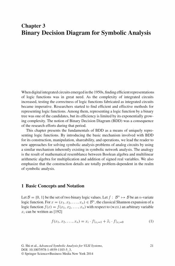
Fig. 1 Graphical representa-tion of Shannon expansion off(x) w.r.t. xi
(x)
i
xi
xi
xix
i
f(x)
f (x)f
x
where f |xi=b := f(x1, . . . ,xi−1, b,xi+1, . . . ,xn) is the function f by restrictingthe variable xi to a constant b ∧ B. Since the restriction of a logic function remainsa logic function, the Shannon expansion (1) can be repeated until the ultimatelyrestricted logic functions become a constant true (i.e., 1) or false (i.e., 0). Obviously,this is a binary decomposition process.
The two factors f |xi=1 and f |xi=0 in (1) are called the cofactors of f(x) w.r.t.the literals xi and xi (the negate of xi), respectively. For convenience, the followingnotations are used throughout the book:
fxi(x) := f(x)|xi=1, (2a)
fxi(x) := f(x)|xi=0. (2b)
The one-step Shannon expansion (or decomposition) of f(x) w.r.t. the variablexi can be represented graphically as shown in Fig. 1. The variable xi enclosed in acircle is called a BDD node or BDD vertex. Two arrows (or directed edges) pointfrom the vertex down to the two cofactors fxi(x) and fxi(x). The solid arrow isattached with the literal xi, meaning that the cofactor is taken w.r.t. xi = 1, while thedashed arrow is attached with the literal xi, meaning that the cofactor is taken w.r.t.xi = 0. The two arrows are referred to as the two decisions taken for the variable xi.Among the three objects involved with the expansion, the variable xi is often calledthe top variable while the two cofactor functions are called the child functions afterthe expansion. It is convenient to use the triple notation
(xi, fxi, fxi) (3)
to represent one-step of Shannon decomposition as illustrated by Fig. 1. In fact, thistriple identifies a function defined by
(xi, fxi, fxi) := xi · fxi(x) + xi · fxi(x) = f(x). (4)
Since fxi(x) and fxi(x) are again logic functions, they can be applied with furtherShannon expansions. Analogous to high-order differentiations of a continuous func-tion w.r.t. multiple variables, high-order Shannon cofactors w.r.t. multiple variables

1 Basic Concepts and Notation 23
1
B
C
1 0
C
10
C
1 0
C C
A
C
f = A B C
B
B CB C
C C
0
C
C
B
C
01
B
A
f = A B C
C
B CB C
(a) (b)
Fig. 2 Shannon expansion of an XOR function. a Expansion by binary tree. b Expansion withsharing by BDD
are denoted by fxixj (x) and fxixj (x), etc., where fxixj (x) is just the cofactor offxi(x) w.r.t. xj (xj ⊆= xi), and likewise for fxixj (x).
Given any multivariate logic function, directly applying Shannon decomposi-tions exhaustively and drawing a graphical representation of the binary decom-positions by connecting BDD nodes defined by Fig. 1, we would obtain a binaryShannon expansion tree. Shown in Fig. 2a is an example of exhaustive binary expan-sion of the function f = A ⊕ B ⊕ C , the exclusive-or (XOR) of three variables.Figure 2a has four layers; except for the bottom layer where the terminal values, trueand false are reached, each BDD node in the upper layers is binary-decomposed tocreate subsequent BDD nodes as cofactors. Hence, the number of vertices doublesin each lower layer.
It is easy to inspect that there exist duplicates among the cofactor functions inthe layer where the C vertices lie; there are two cofactors equal to C and two othercofactors equal to C . Such repeated cofactors represented by redundant sub-BDDscan be suppressed by repointing the respective decision arrows to the existing sub-BDDs. Sharing the duplicate cofactor expressions leads to the new BDD shown inFig. 2b, where two vertices in the C-layer are reduced, but the logic function obtainedat the root remains unchanged. Recall that each BDD vertex defines a logic function.Hence, while drawing Fig. 2, we have attached the cofactor functions by pointingarrows from the displayed expressions to the BDD vertices.
The concept of BDD first appeared in the work by Lee [103] in 1959 in the notion of“Binary Decision Program”. This notion did not receive deserved attention until thework by Akers [6] in 1978. Akers formally introduced the name of Binary DecisionDiagram (BDD) and systematically formulated the definition of BDD, and discussedhow to implement a BDD and how to use BDD for testing implementations of logicfunctions. As the integrated circuit technology evolved, it soon became apparentthat Akers’ seminal considerations on BDD are so important that more fundamental
24 3 Binary Decision Diagram for Symbolic Analysis
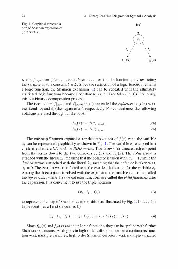
Fig. 3 Equal cofactors
f(x)
i
xj
xix
i
f(x)
x
properties of BDD should be established. The most important property of BDD isunquestionably the canonicity (i.e., uniqueness) of using BDD for logic functionrepresentation. However, canonicity was not addressed in Akers’ work.
2 Canonicity of BDD
A fundamental need in logic synthesis and verification is to find a unique way ofrepresenting logic functions so that two different looking functions can be comparedand identified without checking their truth tables. The need of identifying logicfunctions also exists during the construction of BDD in which sharable cofactorsmust be identified in the most efficient way.
Two things could possibly result in non-uniqueness of a BDD for a logic function.The first thing is concerned with a variablexi that a logic function (or a cofactor) f(x)is independent of. Such a variable is called a don’t-care. In that case, the Shannonexpansion of f(x) w.r.t. the don’t-care variable xi results in two equal cofactors, seethat illustrated in Fig. 3. Specifically, let f(x) = xi · g(x) + xi · h(x), where g(x)and h(x) are two cofactors of f(x). If g(x) = h(x), then it immediately follows thatg(x) = h(x) = f(x), which means that we do not need to create a BDD node for thevariable xi in construction. If such a BDD node is created, it is a superfluous nodeand should be removed in a post-processing phase to compact BDD. The existenceof superfluous nodes also causes the non-uniqueness of BDD. Hence, to have anultimately irreducible BDD, all superfluous nodes should be removed.
On the other hand, the multiplicity of BDD could be caused by expanding agiven function according to different variable orders. Shown in Fig. 4 is such anexample. The function f = ab + cd is Shannon expanded according to the twoorders a < b < c < d and a < c < b < d where the relation ‘<’ indicatesprecedence. In the two BDDs shown in Fig. 4 identical cofactors have been shared.Clearly, the BDD in Fig. 4a is different from that shown in Fig. 4b, and they cannotbe made identical without changing the variable order.

2 Canonicity of BDD 25
a < c < b < d
a
b
c
01
d
a
cc
b
1
d
0b
0
0
F = ab + cd
a < b < c < d
F = ab + cd
Fig. 4 Two BDDs created for the same function f = ab + cd according to two different variableorders: a < b < c < d and a < c < b < d
Suppose we are given two BDDs representing the same function but created bydifferent variable ordering. Then, checking whether the two BDDs indeed representthe same function would not be easy. One might consider creating truth tables, butrunning through all variable values to evaluate the two BDDs is costly.
Because by construction BDD is a bottom-up recursive data structure, all pro-cedures for construction, evaluation, comparison, or even logic operations betweenBDDs should be implemented iteratively, whether by top-down or bottom-up. Astraightforward approach to verifying whether two BDDs indeed represent the samelogic function would be to iteratively compare whether the two Shannon decom-position processes are identical by following a fixed variable order. If yes, then thetwo functions must be equal. To make two BDDs comparable in this sense, the twofunctions for comparison should be constructed in two BDDs by following the sameorder of variables. The following triple-based argument makes the inductive reason-ing much clearer.
Shown in Fig. 5 is the Shannon expansion of a single variable xk (also consideredas a logic function). This single variable function can be written in a triple (xk, 1, 0),in which the first entry is a variable (called a top variable) while the second and thirdentries are two logic functions. Since every BDD node represents a logic functionby a sub-BDD rooted at that node, the second and third entries in a triple also canbe considered as two BDD vertexes (which could be equal if the variable xk is adon’t-care). It is straightforward to compare whether two single-variable functionsrepresented by BDDs as Fig. 5 are identical. This simple observation can be extendedto the following general result.
Proposition 3.1 (Functional Equivalence) Let the variables of a function f(x1,x2,
. . . ,xn) be ordered by the tuple (x1,x2, . . . ,xn). Suppose that two sequentialShannon decompositions have reached two functions f1(xk,xk+1, . . . ,xn) andf2(xk,xk+1, . . . ,xn). Then, f1 = f2 if and only if f1|xk = f2|xk and f1|xk = f2|xk .

26 3 Binary Decision Diagram for Symbolic Analysis
Fig. 5 Shannon expansion ofa single variable
k
xk
1 0
xkx k
x
Proof The equivalence is a direct result of the following two Shannon decomposi-tions:
f1(xk,xk+1, . . . ,xn) = xk · f1|xk + xk · f1|xk ,f2(xk,xk+1, . . . ,xn) = xk · f2|xk + xk · f2|xk .
�
Let V be a BDD vertex, let V .solid and V .dashed be the BDD vertex respectivelypointed by the solid and dashed arrows of vertex V . The following proposition is adirect consequence of Proposition 3.1.
Proposition 3.2 (Shareable Vertex) Suppose that two BDD vertexes V1 and V2have the same variable name. If (V1).solid = (V2).solid and (V1).dashed =(V2).dashed, then vertexes V1 and V2 can be shared.
When two vertexes V1 and V2 can be shared, the second BDD vertex V2 can bereduced by repointing all arrows pointing to V2 to V1.
Propositions 3.1 and 3.2 provide a foundation to the shareability for BDD con-struction. There could be two ways to identify shareability: One is by a top-downconstruction in which equal functions are recognized and shared by creating oneBDD vertex, the other is by a bottom-up scanning of an existing BDD in which twomatched triples indicates a missed sharing during construction. In creating BDD for alogic function, recognizing the former case is harder because we have to compare theequality of two functions without inductive information. Hence, the second methodis preferable, but is used only when a logic BDD has already been created.
Specifically, we scan a BDD from bottom up. If we find that a triple (xk, g, h) hasthe two cofactor pointers g(x) and h(x) pointing to two BDD vertexes in the sameway as an existing triple of the same top variablexk , then the currently scanned vertexof name xk is a reducible vertex. We just re-connect all decision arrows pointing to

2 Canonicity of BDD 27
the current top vertex xk to the existing vertex identified by the triple (xk, g, h).The reducible vertex becomes unreferenced and can be cleaned.
Given a fixed variable order for Shannon expansion, a unique or minimal BDDcan be constructed by sharing all shareable cofactors during the construction phaseor during the bottom-up scanning phase. If all shareable vertexes are shared and allsuperfluous (don’t care) vertexes are removed, a minimal BDD results. A minimalBDD means that there does not exist another BDD of the same variable order repre-senting the same function, but has a less number of BDD vertexes. We also say that aminimal BDD is irreducible. Another popular name for a minimal BDD is ReducedOrdered BDD, i.e., ROBDD, firstly named by the author of [15].
As we said earlier, representing a logic function by a unique BDD is extremelyuseful and important because it can be used for the fingerprint of a logic function.No matter what a logic expression may look like in appearance, its BDD created byfollowing a fixed variable order and enforcing the minimality must be unique. It isalso important to be aware that, in addition to being unique, a minimal BDD cangreatly reduce the complexity of representing a logic function, thereby simplifiesother subsequent logic operations, including logic evaluations. The property can bevery useful in applying BDD to other non-logic combinatorial problems.
Identifying a cofactor by a triple was originally contributed by Akers [6]. However,the additional attribute of variable ordering for canonicity is due to Bryant [14, 15].In addition to emphasizing the canonicity of BDD, Bryant [15] also presented a setof systematic routines for functional operations and compositions on BDDs. Braceet al. [13] further addressed the issues regarding the BDD implementation by using amodern programming language. By all these works, a complete theory on BDD anda set of efficient algorithms for implementation had been established around 1990.
The most valuable application of the BDD canonicity is for logic verification.Since the establishment of this property by Bryant, BDD has become a standardengine for developing formal verification tools [17].
Before ending this section, we mention several commonly used terminologies fordescribing a BDD. An order of variables refer to the order each variable is selectedfor generating cofactors from top (the root) down to the two terminal nodes ‘1’ and‘0’. The variable order for creating a BDD can be arbitrary in general, but it affectsthe occurrence of sharable cofactors, hence the size of a BDD. The size of a BDD isdefined to be the total number vertices connected together to form a BDD (usuallyexcluding the two terminal vertices). Given a variable order, a minimal BDD musthave a minimal size. Hence, the minimal BDD size is also a characteristic of a logicfunction. Finding an optimal order for achieving a minimal BDD for one set of logicproblems is in general an NP-complete problem [55].
A path of BDD refers to a sequence of connected decision arrows from the BDDroot to a terminal. If the path is terminated at the node “1”, it is called a 1-path;otherwise, it is called a 0-path if it is terminated at the node “0”. In BDD a pathrepresents one logic evaluation in that the decisions encountered along the path arethe logic values assigned to the variables. Specifically, if the decision variable is xi,then the value of xi = 1 is assigned; otherwise, the decision variable of xi means

28 3 Binary Decision Diagram for Symbolic Analysis
i
xi
xi
xi(x)g
xi
(x)g
g(x)
AND xi
xi
xi
xi(x)h
xi
h )x(
h(x)
xi
xi
xi
xi
h )x(xi(x)h
xi
(x)gxi(x)g
x
f(x) = g(x)h(x)
Fig. 6 The AND operation by Shannon expansion
that the value of xi = 0 is assigned. The terminal value, 1 or 0, reached by a path isthe resulting function value given the assignment of the variables along the path.
3 Logic Operations on BDDs
Suppose two logic functions g(x) and h(x), x ∧ Bn, have been represented byBDDs according to the same variable order. Let f(x) = g(x) · h(x) be the resultingfunction after applying the AND operation to the two functions g(x) and h(x). TheBDD representation of f(x) can be constructed by directly manipulating the twoexisting BDDs. The manipulation is again based on the Shannon expansion.
Let the variables be ordered by x1 < x2 < · · · < xn. The Shannon expansion off(x) w.r.t. x1 can be written as
f(x) = x1 [g(x)h(x)]x1+ x1 [g(x)h(x)]x1
= x1[gx1(x)hx1(x)
⎡ + x1[gx1(x)hx1(x)
⎡. (5)
Therefore, the cofactors of f(x) w.r.t. x1 are simply gx1(x)hx1(x) and gx1(x)hx1(x),which are just the AND operations on the cofactors of g(x) and h(x) at x1 and x1,respectively, see Fig. 6.
Because the sub-BDDs representing the cofactors gx1 , hx1 , gx1 , and hx1 havealready been created, what we need to do in implementation is to use BDD nodepointers to trace these cofactors by stepping down from father nodes to children nodesin their respective BDDs. Once some of the cofactors have reached the terminal node1 or 0 in their BDDs, the resulting triple can easily be identified and the cofactorrecursion can be terminated. For example, suppose the currently working variableis xk and gxk = 1, then the AND of the two cofactors gxkhxk = hxk and we justreturn the pointer giving the cofactor hxk to the current decision arrow marked byxk. Likewise, we can deal with other terminal cases.

3 Logic Operations on BDDs 29
AND
a
1
01
b
F = a + b
a
0c
01
c
G = ac
a
0c
01
c
FG = ac
Fig. 7 Example of applying AND operation on two BDDs
AND
a
1 b
1 0
F = a + b
a
0c
01
G = ac
a
0
FG = ac
Fig. 8 The resulting BDD by AND operation is shared with the existing BDDs
Figures 7 and 8 illustrate the AND operation applied to two functions representedby BDDs: F = a+ b and G = ac. The resulting BDD shown in Fig. 7 has a cofactorwritten in triple (c, 1, 0) which is the result of AND operation of Fa · Ga = (FG)a.Because Fa = 1 is a terminal, we have (FG)a = 1 · Ga = c. Hence, the triple(c, 1, 0) in the BDD representing the function FG is identical to the one in the BDDrepresenting the function G. These two triples can be shared in implementation.Shown in Fig. 8 is the result of sharing the two identical cofactors c. Sharing thecofactors in logic operations is another advantage of using BDD as graphical repre-sentations of logic functions. It can greatly improve the efficiency of logic operationsin a BDD-based logic system.
There are many logic operators in Boolean algebra. It turns out that it is unnec-essary to define a different routine for each type of logic operators. Brace et al.[13] proposed that a single triple composed of three logic function, defined byI T E(F, G, H) = FG + F H , can be used to generate all logic operations inBoolean algebra. Here, “ITE” stands for “If-Then-Else”, meaning that if F holds, weget G; else we get H.

30 3 Binary Decision Diagram for Symbolic Analysis
The logic operation AN D(g,h) can be represented by I T E(g,h, 0) = gh andthe logic operation OR(g,h) can be represented by I T E(g, 1,h) = g+ gh = g+h.Other logic operations can likewise be converted to their respective ITE expressions,see [13] for the details.
It is easy to justify that the following Shannon expansion holds for the ITE oper-ator:
I T E(F,G, H) = xk · I T E⎢Fxk ,Gxk Hxk
⎣ + xk · I T E⎢Fxk ,Gxk , Hxk
⎣. (6)
Again, as the cofactor recursion proceeds, terminal cases will be encountered. It isthe task of implementation to identify the terminal cases and terminate the recursion.The details have been presented in [13]. The reader also can consult [72, Chap. 6]for a more pedagogical presentation.
4 BDD for Algebraic Symbolic Analysis
So far we have introduced the concept of BDD for logic function representationand manipulation. BDD is a canonical representation of logic functions and is alsoan object for logic operations in Boolean algebra. Some researchers have alreadynoticed that the abstraction of BDD is not limited to logic functions. That is, theway binary operations are defined on a logic variable can be extended to other binaryoperations on variables in their own problem field. For example, Minato extended thenotion of logic BDD to a subset system and defined the respective binary decisionsto be whether or not an element is included by one part of subsets [134, 135].
BDD also can be used to represent multilinear functions of the form
f(x) = x1x2x3 + x2x3x4 + x3x4x5 + x4x5x6, (7)
where the variables xk take arbitrary real values. The function f(x) is also in sum-of-product (SOP) form, but the addition and multiplication operate in the sense ofarithmetic algebra. Given the number of variables, called the problem dimension,any such multilinear function in SOP form can be represented by a BDD as well.This type of algebraic functions frequently appear in symbolic analysis of analognetworks. For example, in the Laplace expansion of a determinant or in enumeratingweighted spanning trees of a connected graph, etc.
4.1 BDD for Determinant Expansion
Symbolic network analysis is mainly concerned with the small-signal analysis andattempts to derive an analytical solution of a network response given specific inputand output. Hence, a main task in symbolic analysis of analog networks is to solvea linear algebraic equation of the following form

4 BDD for Algebraic Symbolic Analysis 31
⎤
⎥⎥⎥⎦
a11 a12 · · · a1na21 a22 · · · a2n...
.... . .
...
an1 an2 · · · ann
⎛
⎤
⎥⎥⎥⎦
x1x2...
xn
⎛
=
⎤
⎥⎥⎥⎦
b1b2...
bn
⎛, (8)
where n is the dimension of the unknown variables, which also characterizesthe complexity of a problem. Symbolically solving the unknown vector xT =(x1,x2, . . . ,xn) by Gaussian elimination is possible, but it requires a lengthy man-agement of nested expressions in order to store all intermediate results [153]. Nestedexpressions are seemingly simple, but they have many limitations. For example,nested expressions have problem in numerical evaluation because divisions areinvolved. Also, it would be inefficient to manipulate nested expressions to gener-ate symbolic byproducts like s-expanded forms or to derive sensitivity results.
An alternative way is to use the Cramer’s rule to generate the solution for onecomponent. That is,
xk = det(A(k, b))
det(A), (9)
where A is the coefficient matrix of Eq. (8) and A(k, b) is the matrix resulting fromreplacing the kth column of A by the vector b, the right-hand side of Eq. (8). Insymbolic network analysis, it is usually sufficient to derive one or two unknowncomponents corresponding to the output. Therefore, it is feasible to use the Cramer’srule for symbolic network analysis.
According to Eq. (9), the symbolic solution boils down to finding symbolic expres-sions for two determinants det(A(k, b)) and det(A), which have all columns equalbut one.
If we fully expand an n × n determinant, we would obtain a sum of productterms like the expression given in Eq. (7). In practice, directly generating all suchproduct terms requires a combinational procedure whose exponential complexitygrows rapidly with the dimension n and the density of the matrix. A better approachto suppressing the complexity is to perform the expansion iteratively just like theShannon expansion of logic functions, and seek shareability during the expansion.As a matter of fact, for determinants this approach is indeed feasible and a BDD canbe created to store the expansion process symbolically.
The recursive Laplace expansion procedure is based on the following basic equa-tion similar to Shannon expansion:
det(A) = ai,j(−1)i+j · Minor(A, ai,j) + Rem(A, ai,j), (10)
where ai,j is the (i, j)th entry of matrix A, Minor(A, ai,j) is the determinant ofthe matrix resulting from deleting the row and column intersecting at ai,j , which iscalled a Minor operation, and Rem(A, ai,j) denotes the determinant of the matrixafter setting the entry ai,j to zero, which is called the Rem (i.e., remainder) operationof det(A) by removing the terms multiplied by the factor ai,j . The expression in the

32 3 Binary Decision Diagram for Symbolic Analysis
right-hand side of (10) is bisectional in that the first term has the factor ai,j whilethe second does not. This is understood as a binary decision made on the matrixentry ai,j , which is analogous to the Shannon expansion made on a logic variable.By sequencing all nonzero entries of matrix A in order, a sequence of determinantexpansions can be made by repeatedly applying Eq. (10).
The next issue to be concerned with is the shareability. The two factors (−1)i+j
Minor(A, ai,j) and Rem(A, ai,j) are just like two “cofactors” of det(A) w.r.t.the element ai,j . Note that the dimension of the determinant Minor(A, ai,j) isone less than that of A while the dimension of Rem(A, ai,j) remains unchanged.As long as not both of Minor(A, ai,j) and Rem(A, ai,j) become singular, thebinary expansion as defined by (10) can be repeated until the resulting determinantsbecome either one-dimensional (i.e., scalar) or singular. In the course, we shall findnumerous shareable intermediate determinants of different dimensions. By applyingthe same principle as we have stated for logic BDD, whenever a currently generateddeterminant is found to be equal to an existing determinant previously expanded, weneed not re-expand the current determinant and only have to connect the proper BDDdecision arrow to the existing BDD node. This idea of using BDD for determinantexpansion was originally contributed by Shi and Tan in [195, 196] and the resultingBDD was called Determinant Decision Diagram (DDD).
Of course, the above statement only outlines the basic idea of applying BDDfor generating a symbolic representation of determinant expansion. More detailsregarding how to find a reasonably good variable order and how to find shareabledeterminants are to be introduced in a later chapter dedicated to the DDD method forsymbolic network analysis. A detailed implementation strategy for “finding equaldeterminants” would have several variants. Also, we can establish an optimal orderfor a special class of matrices that are full matrices.
4.2 BDD for Spanning Tree Enumeration
Another problem field in which BDD can be applied effectively is to enumerateall spanning trees of a connected undirected graph. There are many algorithms thatcan be used for generating all spanning trees of a graph by explicit enumerations[57, 136]. However, by applying BDD, many repetitive enumeration steps can beomitted by taking the advantage of sharing. The following discussion once againshows that BDD is particularly useful for non-exhaustive enumeration.
In 1965 Minty published a one-page paper [136], in which he described a binarygraph decomposition procedure for enumerating all spanning trees of a connectedgraph. Minty defined two edge operations called “In” and “Out” and applied themto an ordered sequence of the graph edges. The “In” or “Out” operation to an edgerespectively means to include (i.e., retain) or exclude (i.e., remove) the edge. Applyingsuch binary operations exhaustively to a graph and keeping all intermediate resultswould create a binary decomposition tree in which all paths from root to leaf nodesrepresent all spanning trees.

4 BDD for Algebraic Symbolic Analysis 33
e3e2
3e 4e e4e3
e4
e2e23e 4e
e2e4
e1
e3
e2e4
e1
e3
e1
e3 e4
e1
e4
e2e4
e1
e3
e1 in e1 out
e2 in e2 out e2 in e2 out
e3 oute3 in e3 in e3 outT1=(e1, e2)
T2=(e1, e3) T3=(e1, e4) T4=(e2, e3 ) T5=(e2, e4)
e2e4e3
e4
e1
1
2
31 1
1
1
111
1 11
2 2
2 2 2
2
2
222
3 3 3 3
3 3 3 3
3 3
Fig. 9 Minty algorithm for enumerating all spanning trees of a four-edge graph
Figure 9 shows an example of enumerating five spanning trees of a graph con-taining four edges (shown at the top) by applying the Minty algorithm. The edgesare ordered by e1 < e2 < e3 < e4. As the decomposition proceeds, two termi-nation conditions of the Minty algorithm must be checked: whether the retainededges are enough to form a spanning tree or the newly generated graph becomesdisconnected. The exhaustive decomposition process shown in Fig. 9 leads to fiveterminals, which implies that five spanning trees have been enumerated, T1(e1, e2),T2(e1, e3), T3(e1, e4), T4(e2, e3), and T5(e2, e4), as shown in the figure. Here,T1(e1, e2) denotes the first tree formed by the edges e1 and e2 and likewise for theothers.
With BDD the Minty algorithm can be improved by taking the advantage ofsharing. However, the original form of the binary edge operations defined by Minty isnot amenable to sharing. Fortunately, a simple modification to the graph manipulationquickly solves this problem. Since we wish the subgraphs generated by the edgeoperations can be compared and shared, we should reduce a graph by collapsing theedge whenever this edge is to be included. In this way, after (n − 1) edges havebeen collapsed for a connected graph containing n vertices, the graph must havebeen reduced into a single node and the collapsed edges form one spanning tree. Inthe modified Minty algorithm, we simply delete the edge when an edge is excluded.Therefore, in the binary decision process, the size of the original graph must begradually decreasing either in the number of nodes or in the number of edges.
By the above modification, the binary edge operations become edge Collapseand edge Removal. The reduction process can be terminated upon the validity ofone of the following conditions: (1) only one node remains, (2) the remaining
34 3 Binary Decision Diagram for Symbolic Analysis
T1=(e1, e2)
1
e41
0
0
e4
1
e4e3
e3e4
1
e2e3 e4
e1
2
1
e3 e4e2
2
1
e4e3
2
1
1
2
3
1
2e2
e3 e4
e2 out
T2=(e1, e3)
T3=(e1, e4)
T4=(e2, e3)
T5=(e2, e4)
(disconnected)
(disconnected)
3
1
2
3e3 in e3 out
e2 oute2 in
e1 in
e4 in e4 out
e1 out
e2 in
2
1
1
1
Fig. 10 Minty algorithm improved for sharing subgraphs. Some graph nodes have been renumberedafter edge collapse
edges are insufficient to form a spanning-tree, or (3) the current subgraph is alreadydisconnected.
Figure 10 shows the application of the modified Minty algorithm to the samegraph decomposed in Fig. 9.
Following the graph reduction paths, we see that the subgraph in the middle ofthe third row (containing edges e3 and e4) is shared by the two decision arrows fromthe preceding row. Comparing to the same location in Fig. 9, we see that the twosubgraphs in the middle of the third row in Fig. 9 cannot be shared because the edgese1 and e2 are not collapsed after the “In” operations.
We conclude that the modified Minty algorithm can be used to construct a BDDfor enumerating all spanning trees of a graph. A binary decision is made on eachselected edge by either collapsing or removing this edge. All shareable subgraphsare shared by devising a graph comparison mechanism. Whenever a subgraph isreduced into a single node, the reduction path is terminated at the vertex “1”, whichindicates the completion of a spanning tree. Putting together all “1” nodes and all“0” nodes in Fig. 10, we arrive at the BDD shown in Fig. 11, in which we see thateach BDD vertex is attached with a subgraph on which binary edge operations areapplied to generate new subgraphs in the next layer.

4 BDD for Algebraic Symbolic Analysis 35
2
e3 e4e2
e4
e3
e4
1
e2e3 e4
e1
0
e1
e2
e1 out
e2
e2 in
e3 in
e1 in
e3 out
e4 out
e2
e4e3
e4e3
e2 out e2 in
e2 out
e4 in
T2=(e1, e3),
T1=(e1, e2),
T3=(e1, e4),
T4=(e2, e3),
T5=(e2, e4).
1
2
3
1
2
1
2
1
2
3
1
Fig. 11 Five spanning trees represented in a BDD
During the graph reduction we have introduced a rule for node renumbering whenan edge is collapsed. For the sake of easy implementation, we keep the smaller nodenumber when two terminal nodes are merged, meanwhile a portion of nodes arerenumbered to keep the reduced graph nodes continuously numbered. This noderenumbering strategy makes the graph attached to the BDD vertex e3 in Fig. 11shareable.
The BDD shown in Fig. 11 has five 1-paths that represent the five spanning trees.The spanning trees can be read out from the created BDD as follows: We traversefrom the root vertex down to the terminal vertex “1”. Whenever arriving at a BDDnode, if we go by the solid arrow from the node, then we collect the edge namedby the node; if we go by the dashed arrow from the node, then we skip the edgenamed by the node. Upon reaching the terminal “1”, all the edges collected alongthe path form a spanning tree. In this way we may read five paths starting from theroot vertex to the terminal “1”, which generate five spanning trees (see those listed inFig. 11.) Consequently, we have established a basic principle that a BDD can be usedto implicitly store all spanning trees of a connected graph. This procedure must besignificantly faster than explicitly enumerating all spanning trees. The enumerationspeed by BDD can further be improved by developing better edge ordering heuristics.

36 3 Binary Decision Diagram for Symbolic Analysis
The graphical spanning trees have correspondence to the sum-of-product algebrawhen the graph edges are weighted. The product terms can be generated by multi-plying the edge weights of a spanning tree. Adding all such product terms leads toa symbolic SOP expression. Such expressions are very useful in symbolic networkanalysis.
It is worth noting that the principle of Shannon expansion is now replaced by binarygraph decomposition in the sense of whether or not a graph edge is included in aspanning tree. In addition, the shareable objects now become subgraphs generatedby collapsing or removing edges. With these two fundamental elements, BDD isagain a natural means for efficiently bookkeeping the decomposition process. Theapplication of BDD to the problem of spanning tree enumeration was first proposed in[26, 204], where a graph-pair reduction method was proposed for symbolic analysisof analog networks. A graph comparison mechanism was also developed there foridentifying the subgraph isomorphism for sharing. We shall expand on the details ina later chapter.
4.3 Benefits of Using BDD for Symbolic Analysis
The advantages of using BDD for logic synthesis and verification have been reportedin many places. In contrast, the benefits of using BDD for symbolic network analysishave some common parts and other parts different from logic BDDs. The commonfacts are attributed to the compactness of BDD, which makes it possible to deal witha combinatorial problem implicitly rather than explicitly. This key advantage is dueto sharing enforced in a minimal BDD. Other advantages regarding the applicationof BDD for symbolic analysis of analog networks arise from the problem field itself.We hardly use the BDD for verifying analog networks because the analog circuitverification problem is less of a logic problem. Rather, in most cases we use BDDfor investigating the behavioral dependence of an analog circuit on its device parame-ters, which commonly involve many aspects, like variability, sensitivity, reliability,statistical properties, sizing, matching, biasing, and even the network topology, etc.A symbolic representation in BDD is inherently advantageous for implementing allthese tasks due to its compactness and easily implementable algebraic manipulations.
Traditionally, a symbolic approach to analog circuit analysis is to derive exactor approximate symbolic transfer functions for the corresponding small-signal net-works. Besides using a SPICE tool for large-signal simulations, most of the cir-cuit performance metrics can be investigated by small-signal analysis. In the laterhalf of the 20th century, symbolic circuit analysis methods have been widely stud-ied and countless papers have been published in the literature. Several mono-graphs are recommended for reading to get a historical perspective on this field[45, 49, 52, 60, 117].
Before BDD was introduced to solving a few unknowns from a set of simultaneouslinear equations like (8), many methods had been attempted to symbolically solvethe response of a linear network. Typical methods are (i) direct Laplace determinant

4 BDD for Algebraic Symbolic Analysis 37
expansion, which was used in the well-known ISAAC symbolic simulator [62]published in 1989. (ii) Coates flow-graph [30], which is a graphical method of solv-ing linear equations and was used in [219] published in 1986 to develop a programcalled FLOWUP, and (iii) generating nested expression by Gaussian elimination[153] published in 2001.
The Determinant Decision Diagram method [196] published in 2000 was the firstsymbolic method using BDD for solving a few unknowns of a set of linear equa-tions by determinant expansion. The use of BDD can largely increase the circuit sizeanalyzable by generating exact network formulas due to the strategy of implicit enu-meration. Although the complexity of DDD representation still grows exponentially,the growth rate is much milder than any other direct expansion method.
Another parallel line for symbolic network analysis is by topological analysis;that is, only the network topology is processed during symbolic generation withoutgoing through algebraic matrix formulation and calculations. A common techniqueemployed in topological analysis is by spanning tree enumeration. Before BDDwas introduced to this category of methods, most researches published applied atopological method for approximate symbolic analysis. The main reason was thatmany tree enumeration methods allow ordering the spanning trees by the assignededge weights, therefore it is possible to generate only a portion of product terms byenumerating those spanning trees of dominant weights. The works [255, 258, 273]published in the early half of 1990s mainly took this approach.
The BDD technique was introduced to this category of methods relatively later.The first work proposing to use BDD for spanning tree enumeration was publishedaround 2007 [26, 204]. The incorporation of BDD for generating the symbolic prod-uct terms by enumerating spanning trees implicitly again can greatly improve thesize of circuits solvable by exact symbolic analysis. Moreover, because exact sym-bolic expressions can be constructed in a data structure that can be manipulated,many tasks for behavioral circuit analysis can be carried out by directly applyingalgebraic operations on the BDD. This property was not available in the traditionaltree-enumeration methods because no systematic data storage could be managed inan efficient way.
The applications of BDD in the two lines of methodologies described above havemanifested a basic philosophy: BDD-based implicit construction methods not onlyimprove the solvable problem size, but also greatly enhance the efficiency in thepost-processing stage. This fact forms undoubtedly the fundamental foundation ofthis book dedicated to the old subject of symbolic circuit analysis but by the novelBDD approach.
The advantages of using BDD for exact symbolic circuit analysis are summarizedbelow. These advantages are to be explored in greater details in the succeedingchapters.
1. It frequently occurs in symbolic network analysis that an enormous number ofsub-expressions are common, and to represent them in a shared format BDD isprobably the best choice.

38 3 Binary Decision Diagram for Symbolic Analysis
2. The common sub-expressions are not identified by directly comparing theexpressions themselves, rather they are identified by comparing those objects(determinants or graphs) that generate those expressions. A BDD-based construc-tion is probably the only approach available for taking the advantage of sharingthose intermediately generated objects.
3. Automatically performing sharing while in construction contributes the most totime and storage efficiency. Symbolic enumeration based on a BDD data structurenever runs into exhaustive enumeration.
4. Symbolic expressions represented in BDDs can be highly advantageous for post-processing. Establishing symbolic expressions of a network function is not theend of a symbolic analysis task. Many analysis and synthesis tasks would haveto manipulate the symbolic expressions from which useful circuit insights arederived. Algebraic manipulation on a BDD data structure is easy and efficient.
5. BDD is also a good data structure for efficient numerical evaluation becauseno two equal sub-expressions are evaluated twice. Hence, symbolic expressionscoded in BDD are extremely favorable for repetitive numerical evaluations, forinstance, in Monte Carlo analysis.
6. Sensitivity analysis can provide helpful information in circuit design. Implement-ing a variety of sensitivity analyses based on BDD can be as simple as modifyinga few decision arrows in a BDD. Such convenience might not exist in other formsof symbolic representations.
7. If needed, approximate symbolic expression can be generated directly from aBDD representation.
5 BDD Implementation
The most important feature of BDD is sharing. To implement sharing, a naturalrequirement is on how to define a comparable measure for identifying sharableobjects. A detailed definition of shareability is highly problem-dependent. Some-times one may define several measures for identifying the sharable objects of oneproblem. A choice of shareability measure often could completely change the imple-mentation of a BDD application problem. We shall briefly introduce some basicelements fundamental to the BDD implementation and pay close attention to theproblem nature and its formulation. More details are to be expanded on in the laterchapters where detailed symbolic constructions are described.
As we mentioned before, the most commonly used shareability measure is a BDDtriple, denoted generically by (var, solid, dashed), which is composed of a top vari-able var as a BDD node and two children pointers solid and dashed. Identifying theshareability by matching two triples is a natural choice for logic BDD construction,because logic functions for the same truth table can take so many different forms thatdeveloping a comparison measure by processing the literals describing the functionsis not easy. Since matching a pair of triples like (var, solid, dashed) requires firstlymatching the pointers solid and dashed, it naturally implies that the construction

5 BDD Implementation 39
2f
1
u
p q
f1
f2
u
p q
dashedsolid
f
u
Fig. 12 Illustration of BDD triple-based sharing in bottom-up construction
procedure must be bottom-up. At the lowest level, a triple like (var,&One,&Zero)is easily identified, where &One and &Zero denote respectively the two addresseswhere the terminal nodes “1” and “0” are saved. At an upper level, whenever twodecision pointers point to the same shared objects while the two top variables areequal, then such two triples are identified equal and the address of the first top BDDnode is returned for sharing. This principle is illustrated in Fig. 12.
Suppose the triple (u, f1.solid, f1.dashed) has been constructed, where f1.solidpoints to the node “p” and f1.dashed points to the node “q” (see Fig. 12). Supposethat when we come to work with another triple (u, f2.solid, f2.dashed), the twopointers f2.solid and f2.dashed have already pointed to the two existing nodes “p”and “q”, respectively. Because the current working top variable is also “u”, we aresure that the current triple (u, f2.solid, f2.dashed) must be identical to the previoustriple (u, f1.solid, f1.dashed). Therefore, we do not need to create a new BDDnode named “u” and instead we simply connect the pointer f2 to the existing BDDnode “u”. The resulting connection is as shown on the right-hand side in Fig. 12.This process is performed bottom-up recursively. After the process is completed, theresulting BDD must be canonical in that all shareable triples have been shared.
The triple-based sharing mechanism is used in the construction of logic BDDs,especially in the constructions where the ITE operator is employed [13]. In that case,the two decision pointers in a triple are known by the Shannon cofactors associatedto the ITE operands. The reader is referred to [13] for the details of implementationin this regard.
The triple-based sharing is also employed for reducing a non-canonical BDD tobe canonical. In case a BDD is constructed without the assurance of canonicity, onemay run a Reduce procedure from bottom up to enforce the canonicity [15]. What it isdone in the Reduce procedure is just to re-identify the sharable triples and reconnectsome decision arrows. After the Reduce procedure, redundant sub-BDDs would beproduced whose roots are not referenced (or pointed) by any other BDD arrows.Such sub-BDDs can be removed by running a garbage collection process [13].
Another useful shareability measure is by comparing shareable objects thatare being produced during BDD construction. The shareable objects are problem-dependent. For example, in determinant expansion, the shareable objects are minors(i.e., sub-determinants), and in graph decomposition, the shareable objects aresubgraphs. The object-based sharing measure is commonly used in a top-down

40 3 Binary Decision Diagram for Symbolic Analysis
1
u
dashedsolid
Obj 1 Obj 2
f2
u
f1
f2
u
Obj 1 Obj 2
dashedsolid
Obj 1
f
Obj 2
Fig. 13 Illustration of object-based sharing for top-down BDD construction
construction process. The intermediate objects generated by the decompositions arestored in a hash table. Whenever a new intermediate object is generated, it is com-pared to the objects saved in the hash table. If a match is found, the existing address ofthe object is returned for BDD connection; otherwise, the new object is saved to thehash table for future lookup. The BDD sharing by using this principle is illustratedin Fig. 13.
Implementing BDD by using the technique of identifying triples was first proposedby Akers in [6] in 1978. Later in 1990 Brace et al. [13] further extended this tech-nique by introducing the ITE-based logic operation and the associated triple-basedBDD construction techniques. The ITE technique becomes more useful if numerousequivalences as the intermediate ITE results can be recognized and identified. Thispractice would significantly improve the construction efficiency. In fact, the equiv-alence identification is similar to the object-based shareability measure describedabove which is mainly for a top-down construction.
When BDD was first introduced to symbolic analysis of analog networks in theDDD work [196] in 2000, the top-down construction method by using an object-basedsharing measure was not considered. The original construction method employed in[196] and other subsequent works [197, 233, 236] was based on the analogy to logicBDD constructions; that is, only the triple-based sharing mechanism was adopted inimplementation. This method has several limitations as pointed out later by the work[200] in 2010. Such limitations can be improved by adopting a new implementationtaking the advantage of object-based sharing. It is shown in [199] that a minor (i.e.,sub-determinant) can be uniquely identified by the row and column indexes providedthat the nonzeros of the original full dimensional matrix has been ordered. This basicproposition guarantees that the BDD constructed by using minor-based sharing beautomatically minimal.
One thing that requires special attention in algebraic BDD is that there could besome BDD nodes whose solid arrows point to the terminal “0”. The node “s” shownin the left-hand side BDD in Fig. 14 is such a case. Such cases usually happen whenthe object decomposition processed during construction has reached a void result;say, a singular minor is reached in determinant expansion or it is recognized that adisconnected graph is reached in graph reduction, etc. Connecting a dashed arrow to“0” does not require special attention, whereas connecting a solid arrow to “0” does,because a solid arrow denotes a multiplication. In arithmetic algebra, any number

5 BDD Implementation 41
Fig. 14 Illustration of zero-suppression on an algebraicBDD
p q
0
s
r
p q
r
Fig. 15 Two topologicallynon-identical graphs couldgenerate an equal termG1G2G3
2
1G2G
3G
3
1
0
1G
2G
3G
32
1
0
multiplied by zero is zero. For the left BDD shown in Fig. 14, we would get theexpression (s∗0+ (r ∗p+q)) from the root, which is just the expression (r ∗p+q).Therefore, the s node and its connection to “0” can be removed, meanwhile the arrowpointing at s should be reconnected to the BDD node “r”. This process is called zero-suppression (abbreviated ZS), and was first considered by Minato in [135] when heextended logic BDD to a representation for a subset system. Zero-suppression foran algebraic BDD is just analogous to a superfluous node in logic BDD when itstwo cofactors are equal (see Sect. 2). In implementation, we should be aware ofthe propagation of zero-suppression; namely, suppression of one BDD node causesanother BDD node to be connected to zero by a solid arrow. It is a simple fact that anysteps of zero-suppression do not change the correctness of a symbolic expression,but reduce those redundant BDD nodes, thereby reducing the BDD size.
It is also worth pointing out that some object-based sharing measure could possiblyresult in a non-minimal BDD. This is in particular true in applying BDD for spanningtree enumeration. When we interpret spanning trees as product terms, it could happenthat two spanning trees of different topology could likely generate the same term.Shown in Fig. 15 is such an example. There are two trees connecting the same set offour nodes. The reason why identically named edges are connected to different nodesis because we have to renumber node numbers when an edge is collapsed and twoterminal nodes of the edge become one. Node renumbering could result in the casethat edges of the same name are connected to different nodes. Without completelydecomposing the graphs like that shown in Fig. 15, we are not sure whether suchtwo graphs would generate an identical term. In a top-down construction, such twographs are just considered different, i.e., non-shareable. However, after the BDDconstruction is completed, we would find some duplicate sub-BDDs, which should becompacted. In this occasion, the Reduce for minimality procedure mentioned abovecan be employed. A bottom-up scan of the whole BDD can remove all redundantBDD nodes to come up with a canonical BDD [26].

42 3 Binary Decision Diagram for Symbolic Analysis
6 Summary
This chapter has introduced the basic concepts of BDD as a compact data structure forrepresenting a combinational set of terms consisting of a finite set of literals, whichcould be either a logic function or an algebraic multilinear function in sum-of-productforms. The Shannon expansion and its equivalence in other problem fields playthe fundamental role of defining binary decisions and the way how the subsequentcomputational objects are generated. Since BDD was originally created for logicfunctions and well-known in the community of logic synthesis field, we have madeefforts on introducing the basic notions of BDD without getting into too much detailson their applications, because they are widely available in the existing literature.
In the meanwhile, we have made extra efforts on introducing the less well-knownapplications of BDD to the field of analog network analysis, by paying a specialattention to the two particular approaches, matrix-based determinant expansion andcircuit topology-based spanning-tree enumeration. These two types of methodolo-gies, reformulated in BDDs, are the main subject of this book. In the followingchapters, more detailed materials and contributions achieved in the past fifteen yearsor so are introduced. Besides establishing the detailed algorithms, we also wouldmake quite an amount of effort on exploring the usefulness in the application toanalog design automation problems. It seems that a BDD-based symbolic approachto analog circuit analysis and design is more intriguing in the sense of algorithmdesign and software implementation.

Part IIMethods
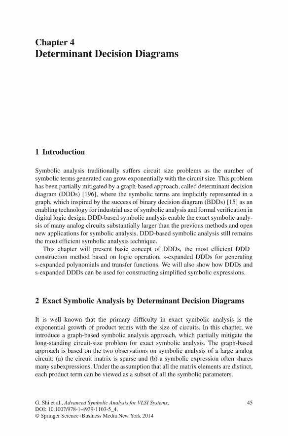
Chapter 4Determinant Decision Diagrams
1 Introduction
Symbolic analysis traditionally suffers circuit size problems as the number ofsymbolic terms generated can grow exponentially with the circuit size. This problemhas been partially mitigated by a graph-based approach, called determinant decisiondiagram (DDDs) [196], where the symbolic terms are implicitly represented in agraph, which inspired by the success of binary decision diagram (BDDs) [15] as anenabling technology for industrial use of symbolic analysis and formal verification indigital logic design. DDD-based symbolic analysis enable the exact symbolic analy-sis of many analog circuits substantially larger than the previous methods and opennew applications for symbolic analysis. DDD-based symbolic analysis still remainsthe most efficient symbolic analysis technique.
This chapter will present basic concept of DDDs, the most efficient DDDconstruction method based on logic operation, s-expanded DDDs for generatings-expanded polynomials and transfer functions. We will also show how DDDs ands-expanded DDDs can be used for constructing simplified symbolic expressions.
2 Exact Symbolic Analysis by Determinant Decision Diagrams
It is well known that the primary difficulty in exact symbolic analysis is theexponential growth of product terms with the size of circuits. In this chapter, weintroduce a graph-based symbolic analysis approach, which partially mitigate thelong-standing circuit-size problem for exact symbolic analysis. The graph-basedapproach is based on the two observations on symbolic analysis of a large analogcircuit: (a) the circuit matrix is sparse and (b) a symbolic expression often sharesmany subexpressions. Under the assumption that all the matrix elements are distinct,each product term can be viewed as a subset of all the symbolic parameters.
G. Shi et al., Advanced Symbolic Analysis for VLSI Systems, 45DOI: 10.1007/978-1-4939-1103-5_4,© Springer Science+Business Media New York 2014

46 4 Determinant Decision Diagrams
Determinant decision diagrams (DDDs) was introduced to represent determinantssymbolically [196]. DDDs is essentially Zero-suppressed Binary Decision Diagrams(ZBDDs)—introduced originally for representing sparse subset systems [134]. AZBDD is a variant of a Binary Decision Diagram (BDD) introduced by Akers [6]and popularized by Bryant [15]. BDDs have brought a great success to the formalverification and testing for combinational and sequential digital circuits [15, 72].DDD representation has several advantages over both the expanded and arbitrarilynested forms of a symbolic expression. First, similar to the nested form, our repre-sentation is compact for a large class of analog circuits. A ladder-structured networkcan be represented by a diagram where the number of vertices in the diagram (calledits size) is equal to the number of symbolic parameters. As indicated by [196], thetypical size of DDD is dramatically smaller than that of product terms. For instance,5.71×1020 terms can be represented by a diagram with 398 vertices. Second, similarto the expanded form, our representation is canonical, i.e., every determinant has aunique representation, and is amenable to symbolic manipulations.
3 DDD Representation of Symbolic Determinant
In this section, we formally introduce determinant decision diagrams to represent asymbolic matrix determinant. DDD is actually a canonical representation for matrixdeterminants, similar to BDD for representing binary functions and ZBDD for rep-resenting subset systems.
A key observation is that the circuit matrix is sparse and that many times, asymbolic expression may share many subexpressions. For example, consider thefollowing determinant
det (M) =
∣∣∣∣∣∣∣∣
a b 0 0c d e 00 f g h0 0 i j
∣∣∣∣∣∣∣∣
= adg j − adhi − ae f j − bcg j + cbih. (1)
We note that subterms ad, g j , and hi appear in several product terms, and eachproduct term involves a subset (four) out of ten symbolic parameters. Therefore,we view each symbolic product term as a subset, and use a ZBDD to represent thesubset system composed of all the subsets each corresponding to a product term.Figure 1 illustrates the corresponding ZBDD representing all the subsets involved indet (M) under ordering a > c > b > d > f > e > g > i > h > j . It can be seenthat subterms ad, g j , and ih have been shared in the ZBDD representation.
Following directly from the properties of ZBDDs, we have the followingobservations. First, given a fixed order of symbolic parameters, all the subsets ina symbolic determinant can be represented uniquely by a ZBDD. Second, every1-path in the ZBDD corresponds to a product term, and the number of 1-edges inany 1-path is n. The total number of 1-paths is equal to the number of product termsin a symbolic determinant.

3 DDD Representation of Symbolic Determinant 47
Fig. 1 A ZBDD representing{adgi, adhi, a f ej, cbg j, cbih}under ordering a > c > b >
d > f > e > g > i > h > j
i
1 0
a
c
bfg
j e
d
1 edge
0 edge
h
We can view the resulting ZBDD as a graphical representation of the recursiveapplication of the determinant expansion with the expansion order a, c, b, d, f, e, g,i, h, j . Each vertex is labeled with the matrix entry with respect to which the deter-minant is expanded, and it represents all the subsets contained in the correspondingsubmatrix determinant. The 1-edge points to the vertex representing all the subsetscontained in the cofactor of the current expansion, and 0-edge points to the vertexrepresenting all the subsets contained in the remainder.
To embed the signs of the product terms of a symbolic determinant into itscorresponding ZBDD, we associate each vertexv with a sign, s(v), defined as follows:
1. Let P(v) be the set of ZBDD vertices that originate the 1-edges in any 1-pathrooted at v. Then
s(v) =⎡
x≤P(v)
sign(r(x) − r(v)) sign(c(x) − c(v)), (2)
where r(x) and c(x) refer to the absolute row and column indices of vertex x inthe original matrix, and u is an integer so that
sign(u) =⎢
1 if u > 0,−1 if u < 0.
2. If v has an edge pointing to the 1-terminal vertex, then s(v) = +1.
This is called the sign rule. For example, in Fig. 2, shown beside each vertexare the row and column indices of that vertex in the original matrix, as well as the

48 4 Determinant Decision Diagrams
(3,4)
1 0
a
c
bfg
j e
d
1 edge
0 edge
(1,1)
(2,2)
(3,3)
(4,4)
(2,1)
(1,2)
(3,2)
(2,3)
+
+-
+
+
+-
+
-
+(4,3)i
h (3,4)
1 0
a
c
bfg
j e
d
1 edge
0 edge
(1,1)
(2,2)
(3,3)
(4,4)
(2,1)
(1,2)
(3,2)
(2,3)
+
+-
+
+
+-
+
-
+(4,3)i
h
Fig. 2 A signed ZBDD for representing symbolic terms
sign of that vertex obtained by using the sign rule above. For the sign rule, we havefollowing result:
Theorem 1 The sign of a DDD vertex v, s(v), is uniquely determined by (2), andthe product of all the signs in a path is exactly the sign of the corresponding productterm.
For example, consider the 1-path acbgih in Fig. 2. The vertices that originate allthe 1-edges are c, b, i, h, their corresponding signs are −, +, − and +, respectively.Their product is +. This is the sign of the symbolic product term cbih.
With ZBDD and the sign rule as two foundations, we are now ready to introduceformally our representation of a symbolic determinant. Let A be an n×n sparse matrixwith a set of distinct m symbolic parameters {a1, . . . , am}, where 1 ∈ m ∈ n2. Eachsymbolic parameter ai is associated with a unique pair r(ai ) and c(ai ), which denote,respectively, the row index and column index of ai . A determinant decision diagramis a signed, rooted, directed acyclic graph with two terminal vertices, namely the0-terminal vertex and the 1-terminal vertex. Each nonterminal vertex ai is associatedwith a sign, s(ai ), determined by the sign rule defined by (2). It has two outgoingedges, called 1-edge and 0-edge, pointing, respectively, to Dai and Dai . A determi-nant decision graph having root vertex ai denotes a matrix determinant D definedrecursively as
3 DDD Representation of Symbolic Determinant 49
1 0
a
c
bfg
j e
dd(gj-hi)-f(ej)-c(b(gj-hi)]
a[d(gj-hi)-f(ej)]-c[b(gj-hi)]
gj-hi -f(ej) b(gj-hi)
je-hij
1 edge
0 edge
-
-
-
h
i
h
Fig. 3 A determinant decision diagram for matrix M
1. If ai is the 1-terminal vertex, then D = 1.2. If ai is the 0-terminal vertex, then D = 0.3. If ai is a nonterminal vertex, then D = ai s(ai ) Dai + Dai .
Here s(ai )Dai is the cofactor of D with respect to ai , Dai is the minor of D withrespect to ai , Dai is the remainder of D with respect to ai , and operations are algebraicmultiplications and additions. For example, Fig. 3 shows the DDD representation ofdet (M) under ordering a > c > b > d > f > e > g > i > h > j .
To enforce the uniqueness and compactness of the DDD representation, the threerules of ZBDDs, namely, zero-suppression, ordered, and shared are adopted. Thisleads to DDDs having the following properties:
• Every 1-path from the root corresponds to a product term in the fully expandedsymbolic expression. It contains exactly n 1-edges. The number of 1-paths is equalto the number of product terms.
• For any determinant D, there is a unique DDD representation under a given vertexordering.
We use |DDD| to denote the size of a DDD, i.e., the number of vertices in the DDD.Formally, a DDD is a signed, rooted, directed acyclic graph with two terminal
nodes, namely the 0-terminal node and the 1-terminal node. Each non-terminal DDDnode is labeled by a symbol in the determinant denoted by ai (a to j in Fig. 3), anda positive or negative sign denoted by s(ai ). It originates two outgoing edges, called
50 4 Determinant Decision Diagrams
1-edge and 0-edge. Each node ai represents a symbolic expression D(ai ) definedrecursively as follows:
D(ai ) = ai · s(ai ) · Dai + Dai , (3)
where Dai and Dai represent, respectively, the symbolic expressions of the nodespointed by the 1-edge and 0-edge of ai . The 1-terminal node represents expression 1,whereas the 0-terminal node represents expression 0. For example, node h (in Fig. 3)represents expression h, and node i represents expression −ih, and node g representsexpression g j − ih. We also say that a DDD node g represents an expression definedthe DDD subgraph rooted at g. For each node, there are two values, vself and vtree.In (3), vself represents the value of the element itself, which is Dai ; while the vtreerepresents the value of the whole tree (or subtree), which is D(ai ).
A 1-path in a DDD corresponds with a product term in the original DDD, whichis defined as a path from the root node (a in our example) to the 1-terminal includingall symbols and signs of the nodes that originate all the 1-edges along the 1-path. Inour example, there exist five 1-paths representing five product terms: adg j , adhi ,ae f j , bcg j , and cbih. The root node represents the sum of these product terms. Sizeof a DDD is the number of DDD nodes, denoted by |DDD|.
Once a DDD has been constructed, its numerical values of the determinant itrepresents can be computed by performing the depth-first type search of the graphand performing (3) at each node, whose time complexity is linear function of the sizeof the graphs (its number of nodes). The computing step is call Evaluate(D) whereD is a DDD root.
A key problem in many decision diagram applications is how to select a vertexordering, since the size of the resulting decision diagram strongly depends on thechosen ordering. A efficient DDD vertex ordering heuristic has been developed,which can lead to the optimal vertex ordering for a class of circuit matrices, calledband matrices [159, 196].
4 Manipulation of Determinant Decision Diagrams
In this section, we show that, using determinant decision diagrams, algorithms neededfor symbolic analysis and its applications can be performed with the time complexityproportional to the size of the diagrams being manipulated, not the number of 1-pathsin the diagrams, i.e., product terms in the symbolic expressions. Hence, as long asthe determinants of interest can be represented by reasonably small graphs, ouralgorithms are quite efficient.
A basic set of operations on matrix determinants is summarized in Table 1.Most operations are simple extensions of subset operations introduced by Minatoon ZBDDs [134]. These few basic operations can be used directly and/or combinedto perform a wide variety of operations needed for symbolic analysis. In this section,we first describe these operations, and then use an example to illustrate the main

4 Manipulation of Determinant Decision Diagrams 51
Table 1 Summary of basic operations
Determinant operation Result Subset operation
VertexOne() return 1 Base()VertexZero() return 0 Empty()Cofactor(D, s) return the cofactor of D wrt s Subset1(D, s)Remainder(D, s) return the remainder of D wrt s Subset0(D, s)Multiply(D, s) return s × D Change(D, s)Subtract(D, P) return D − P Diff(D, P)Union(D, P) return D + P Union(D, P)Evaluate(D) return the numerical value of D –
ideas of these operations and how they can be applied to compute network functionsensitivities—a key operation needed in optimization and testability analysis. We alsoshow that the generation of significant product terms can be cast as the k-shortestpath problem in a DDD and solved elegantly in time O(k · |DDD|) (Fig. 4).
4.1 Implementation of Basic Operations
We summarize the implementation of these operations in Fig. 1. For the clarity of thedescription, the steps for computing the signs associated with DDD vertices, usingthe sign rule defined in Sect. 3, are not shown.
As the basis of implementation, we employ two techniques originally developedby Brace, Rudell and Bryant for efficiently implementing decision diagrams [13].First, a basic procedure GetVertex(top, D1, D0) is to generate (or copy) a vertexfor a symbol top and two subgraphs D1 and D0. In the procedure, a hash table isused to keep each vertex unique, and vertex elimination and sharing are managedmainly by GetVertex. With GetVertex, all the operations for DDDs we need aredescribed in Fig. 1.
Second, similar to conventional BDDs, we use a cache to remember the resultsof recent operations, and refer to the cache for every recursive call. In this way, wecan avoid duplicate executions for equivalent subgraphs. This enables us to executethese operations in a time linearly proportional to the size of a graph.
Evaluation: Given a determinant decision diagram pointed to by D and a setof numerical values for all the symbolic parameters, Evaluate(D) computes thenumerical value of the corresponding matrix determinant. Evaluate(D) naturallyexploits subexpression sharing in a symbolic expression, and has time complexitylinear in the size of the diagram.
Cofactor and Derivative: Cofactor(D, s) is to compute the cofactor of asymbolic determinant D represented by a DDD with respect to symbolic parameters. It is exactly the derivative of D with respect to s. Cofactor is perhaps the most

52 4 Determinant Decision Diagrams
Cofactor(D, s)1 if (D.top < s) return VertexZero()2 if (D.top = s) return D13 if (D.top > s) return GetVertex(D.top,
Cofactor(D0, s), Cofactor(D1, s))
Multiply(D, s)1 if (D.top < s) return GetVertex(s, 0, D)2 if (D.top = s) return GetVertex(s,D1, D0)3 if (D.top > s) return GetVertex(D.top,
Multiply(D0, s), Multiply(D1, s))
Remainder(D, s)1 if (D.top < s) return D2 if (D.top = s) return D03 if (D.top > s) return GetVertex(D.top,
Remainder(D0, s), Remainder(D1, s))
Union(D,P )1 if (D = 0) return P2 if (P = 0) return D3 if (D = P ) return P4 if (D.top > P.top) return GetVertex(D.top, Union(D0, P ),D1)5 if (D.top < P.top) return GetVertex(P.top, Union(D,P0), P1)6 if (D.top = P.top)
return GetVertex(D.top,Union(D0, P0), Union(D1, P1))
Subtract(D,P )1 if (D = 0) return VertexZero()2 if (P = 0) return D3 if (D = P ) return VertexZero()4 if (D.top > P.top) return GetVertex(D.top, Subtract(D0, P ),D1)5 if (D.top < P.top) return Subtract(D,P0)6 if (D.top = P.top)
return GetVertex(D.top, Subtract(D0, P0), Subtract(D1, P1))
Evaluate(D)1 if (D = 0) return 02 if (D = 1) return 13 return Evaluate(D0) + s(D) * D.top * Evaluate(D1)
Fig. 4 Implementation of basic operations for symbolic analysis
important operation in symbolic analysis of analog circuits. For example, the networkfunctions can be obtained by first computing some cofactors, and then combiningthese cofactors according to some rules (Cramer’s rule).

5 DDD Construction by Logic Operations 53
5 DDD Construction by Logic Operations
One important problem for DDD-based symbolic analysis is to generate the DDDgraphs for a given determinant. One simple way to construct the DDD is by means ofLaplace expansion and building the DDD graphs by means of basic DDD operationsshown in Table 1 as done in [159, 196]. However, such explicit and sequential gen-eration method can lead to exponential construction time even the final DDD sizesdo not grow exponentially [117].
In this section, we look at the generation side of the symbolic analysis problem.We present a novel approach to generating all the symbolic expressions implicitlyand simultaneously. The new approach is inspired by the symbolic approach topointer analysis for compilation optimization [282] where logic functions are used toconstruct the symbolic invocation graphs. The main idea of the new approach is thatthe symbolic expression generation is viewed as a logic circuit synthesis process,and we design a logic circuit that can detect whether or not a symbolic term a validproduct term from a determinant. The logic circuit, which is essentially a Booleanfunction, can be represented by binary decision diagrams (BDDs). BDDs are thentrivially transformed into zero-suppressed binary decision diagrams(ZBDDs), whichare essentially DDD representation of the determinant.
The most important advantage of the new approach over existing ones is that thetime complexity is no longer tied to the number of product terms but depends on theimplicit representation of designed logic during the entire construction process. Thismakes the symbolic analysis problem much more tractable as sizes of BDD/DDDgraphs typically grow very slowly with circuit sizes given a good variable ordering.The new symbolic analysis method shows an inherent relationship between circuitsimulation and logic synthesis for the first time.
5.1 Terms-Detecting Logic for a Determinant
The DDD graph is introduced to represent a determinant. It essentially represents allthe product terms in the determinant. In a DDD graph, each product term correspondsto an 1-path from the root vertex to the 1-terminal. If we view a DDD graph as aBDD graph, where each symbol in a product term takes true Boolean value, all theother symbols take false Boolean value, then the DDD essentially represents thelogic that detects if a given symbolic term is a product term in the determinant, as avalid product term always corresponds to an 1-path, and thus satisfies the logic.
This motivates us to generate the DDD graph by constructing a logic circuit whichis able to detect if a given product term is a valid one from the determinant. This turnsout to be an easy design problem. Indeed, from the definition of determinant [67],we can design a logic to check whether the rows and columns of all the elements ina symbolic term cover every row and column of the matrix exactly once.
Figure 5 shows a portion of the logic schematic for checking whether a givenproduct term is valid from an n×n matrix. We simply compare the row/column index

54 4 Determinant Decision Diagrams
...
... ...
... ...
12
N
12n
abcde000010001000100
f111... ...
... ...
... ...
a11
a21
an1
T1
frow
Tn
Fig. 5 The logic circuit for detecting a valid product term from a determinant
of each nonzero element in this product term with the index of each row/column andexamine if each row/column index appears exactly once.
The logic in Fig. 5 checks for row 1 (encoded as 001 since 3 bit binary codingis used in this example). a11, a21 . . . ann are the elements in the product term to bechecked, 001, 010 . . . , b2b1b0 are the binary codes for all row indices in the matrix.T1 is true only when one of its inputs is true, ensuring that exactly one nonzeroelement is in row 1. Comparators C1 to CN compare the row index of each nonzeroelement with the row index of row 1 (N is the total number of nonzero elements inthe matrix). The AND gate in the last stage makes sure that all the row indices of thematrix are present in the product term. The resulted Boolean function for the rowindex legality check is frow.
We can do the same for the column index legality check where each nonzeroelement is compared with the column index of each column. The resulting logicfunction for column index legality check is fcol . Since both row and column legalityconditions must be satisfied to make a valid product term, the final logic is theconjuncture (AND operation) of two logic functions:
fdet = frow ∧ fcol = frow fcol (4)
where ∧ operation is the logic AND operation. We may also write the frow ∧ fcol asfrow fcol in the sequel. The resulting logic fdet is the Boolean logic we are looking for.
5.2 Logic Operation Based DDD Construction Algorithm
In this section, we show that the logic circuit shown in Fig. 5 can be further simplifiedand the DDD construction can be performed efficiently by a number of simple logicoperations.

5 DDD Construction by Logic Operations 55
5.2.1 Efficient BDD Construction For the Determinant Detecting Logic
For the determinant detecting logic circuit in Fig. 5, we observe that if the nonzeroelement ai j is not in row 1, then the comparison result will always be 0 (i.e., Ci isalways 0). On the other hand, if the ai j is in row 1, the Ci will be ai j where ai j is aBoolean variable. Suppose that row 1 has three nonzero elements a11 a12 and a13,then we have
T1 = a11a12a13 + a11a12a13 + a11a12a13, (5)
where “+” is the OR operation. As a result, we conclude that each nonzero elementin a row i will generate a product term for each row’s uniqueness checking functionTi . In the product term of each nonzero element, the corresponding nonzero elementwill take true Boolean value while the rest nonzero elements in the same row willtake false Boolean value. So every nonzero element in a determinant will generateone product term for constructing frow.
For a n × n matrix, the row legality checking function frow become:
frow = T1 ∧ T2 . . . ∧ Tn (6)
We do the same for generating the column legality check function fcol where everynonzero element generates one product term also for fcol . We can directly buildthose product terms from a determinant by inspection, which simplifies the BDDconstruction considerably. Theoretically, we have
Theorem 2 A product term is a valid one product term of a given matrix determinantdet (A) if and only if (after the product term is transformed into a Boolean expression),it satisfies the Boolean function fdet (A)(= frow∧fcol ). frow and fcol are defined abovefor determinant det (A).
In the following, we illustrate such construction using a simple 2 × 2 determinantdet (A2×2) as shown below:
det (A2×2) =∣∣∣∣a11 0a21 a22
∣∣∣∣ = a11a22.
Determinant det (A2×2) only has one product term a11a22. We now show howthis product term can be generated by using the aforementioned logic circuit.
First, we construct row legality check Boolean function frow. For row 1, we haveTr,1 = a11. For row 2, we have Tr,2 = a21a22 + a21a22. As a result, frow becomes
frow = Tr,1 ∧ Tr,2 = a11(a21a22 + a21a22)
Then we construct column legality check Boolean function fcol . For column 1, wehave Tc,1 = a11a21 + a11a21. For the column 2, we have Tc,2 = a22. As a result,fcol becomes
fcol = Tc,1 ∧ Tc,2 = a22(a11a21 + a11a21)
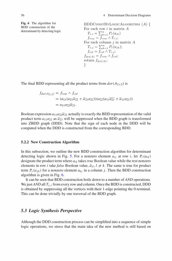
56 4 Determinant Decision Diagrams
Fig. 6 The algorithm forBDD construction of thedeterminant by detecting logic
BDDConstByLogicAlgorithm (A) {For each row i in matrix ATr,i = n
k=1 Pr(aik)frow = frow ∧ Tr,i;
For each column j in matrix ATc,j = n
k=1 Pc(ajk);fcol = fcol ∧ Tc,j ;
fdet(A) = frow ∧ fcol;return fdet(A);}
The final BDD representing all the product terms from det (A2×2) is
fdet (A2×2) = frow ∧ fcol
= (a11(a21a22 + a21a22))(a22(a11a21 + a11a21))
= a11a22a21.
Boolean expression a11a22a21 actually is exactly the BDD representation of the validproduct term a11a22 as a21 will be suppressed when the BDD graph is transformedinto ZBDD graph (DDD). Note that the sign of each node in the DDD will becomputed when the DDD is constructed from the corresponding BDD.
5.2.2 New Construction Algorithm
In this subsection, we outline the new BDD construction algorithm for determinantdetecting logic shown in Fig. 5. For a nonzero element ai j at row i , let Pr (aik)
designate the product term where aik takes true Boolean value while the rest nonzeroelements in row i take false Boolean value, ail , l ⊆= k. The same is true for productterm Pc(a jk) for a nonzero element akj in a column j . Then the BDD constructionalgorithm is given in Fig. 6.
It can be seen that BDD construction boils down to a number of AND operations.We just AND all Tx,i from every row and column. Once the BDD is constructed, DDDis obtained by suppressing all the vertices with their 1-edge pointing the 0-terminal.This can be done trivially by one traversal of the BDD graph.
5.3 Logic Synthesis Perspective
Although the DDD construction process can be simplified into a sequence of simplelogic operations, we stress that the main idea of the new method is still based on
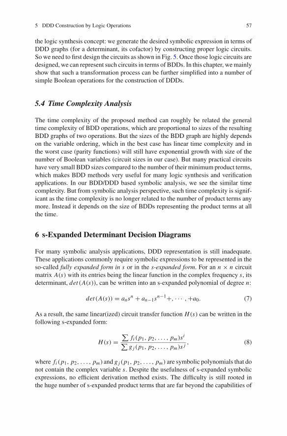
5 DDD Construction by Logic Operations 57
the logic synthesis concept: we generate the desired symbolic expression in terms ofDDD graphs (for a determinant, its cofactor) by constructing proper logic circuits.So we need to first design the circuits as shown in Fig. 5. Once those logic circuits aredesigned, we can represent such circuits in terms of BDDs. In this chapter, we mainlyshow that such a transformation process can be further simplified into a number ofsimple Boolean operations for the construction of DDDs.
5.4 Time Complexity Analysis
The time complexity of the proposed method can roughly be related the generaltime complexity of BDD operations, which are proportional to sizes of the resultingBDD graphs of two operations. But the sizes of the BDD graph are highly dependson the variable ordering, which in the best case has linear time complexity and inthe worst case (parity functions) will still have exponential growth with size of thenumber of Boolean variables (circuit sizes in our case). But many practical circuitshave very small BDD sizes compared to the number of their minimum product terms,which makes BDD methods very useful for many logic synthesis and verificationapplications. In our BDD/DDD based symbolic analysis, we see the similar timecomplexity. But from symbolic analysis perspective, such time complexity is signif-icant as the time complexity is no longer related to the number of product terms anymore. Instead it depends on the size of BDDs representing the product terms at allthe time.
6 s-Expanded Determinant Decision Diagrams
For many symbolic analysis applications, DDD representation is still inadequate.These applications commonly require symbolic expressions to be represented in theso-called fully expanded form in s or in the s-expanded form. For an n × n circuitmatrix A(s) with its entries being the linear function in the complex frequency s, itsdeterminant, det (A(s)), can be written into an s-expanded polynomial of degree n:
det (A(s)) = ansn + an−1sn−1+, · · · ,+a0. (7)
As a result, the same linear(ized) circuit transfer function H(s) can be written in thefollowing s-expanded form:
H(s) =⎣
fi (p1, p2, . . . , pm)si⎣
g j (p1, p2, . . . , pm)s j, (8)
where fi (p1, p2, . . . , pm) and g j (p1, p2, . . . , pm) are symbolic polynomials that donot contain the complex variable s. Despite the usefulness of s-expanded symbolicexpressions, no efficient derivation method exists. The difficulty is still rooted inthe huge number of s-expanded product terms that are far beyond the capabilities of

58 4 Determinant Decision Diagrams
Fig. 7 An example circuit 1 R2 R3
C2 C3R1 C1
2 3
I
symbolic analyzers using traditional methods. Although the numerical interpolationmethod can generate s-expanded expressions, only complex frequency s is kept as asymbol. This method also suffers the numerical problem due to the ill-conditionedequations for solving for numerical coefficients, and thus has limited applications.
We present an efficient algorithm of constructing an s-expanded DDD from anoriginal DDD. If the maximum number of admittance parameters in an entry of acircuit matrix is bounded (true for most practical analog circuits), we prove that boththe size of the resulting s-expanded DDD and the time complexity of the construc-tion algorithm is O(m|D|), where m is the highest power of s in the s-expandedpolynomial of the determinant of the circuit matrix and |D| is the size of the originalDDD D representing the determinant. Experimental results indicate that the numberof DDD vertices used can be many orders-of-magnitudes less than that of productterms represented by the DDDs.
With s-expanded expressions, approximation on symbolic transfer functions canbe performed very efficiently (see Sect. 7). In addition, symbolic poles and zerospartial symbolic analysis and symbolic circuit-level noise analysis and modelingmethod can be performed [159, 227].
6.1 s-Expanded Symbolic Representation
In this section, we introduce the concept of s-expanded determinant decision dia-grams. Instead of presenting the concept in a formal way, we illustrate it through acircuit example.
Consider a simple circuit given in Fig. 7. By using the nodal formulation, itscircuit matrix can be written as
v1v2v3
⎤
⎥⎦
1R1
+ sC1 + 1R2
− 1R2
0− 1
R2
1R2
+ sC2 + 1R3
− 1R3
0 − 1R3
1R3
+ sC3
⎛ .
In modified nodal analysis formulation, the admittance of each circuit or lumpedcircuit parameter, pi , arrives in the circuit matrix in one of three forms—gi , ci s

6 s-Expanded Determinant Decision Diagrams 59
and 1/(l1s)—for the admittance of resistances and capacitances and inductances,respectively. To construct DDDs, we need to associate a label with each entry of acircuit matrix. We call this procedure labeling scheme.
Instead of labeling one symbol for each matrix entry, we label each admittanceparameter in the entries of the circuit matrix when deriving the s-expanded DDDs.Depending on how the circuit parameters are labeled, an s-expanded DDD comesin two forms: (i) In the first labeling scheme, all the circuit parameters in an entryof circuit matrix are first lumped together according to their admittance type, andeach lumped admittance parameter is then represented by a unique symbol. (ii) Inthe second labeling scheme, we label each admittance of circuit parameters by aunique symbol. Obviously the second labeling scheme will generate more productterms than the first. The selection of labeling schemes depends on the applicationsof symbolic analysis. In this chapter, we present both labeling schemes along withtheir implementations.
By the first labeling scheme, we can rewrite the circuit matrix of the examplecircuit as follows: ⎤
⎦a + bs c 0
d e + f s g0 h i + js
⎛ ,
where a = 1R1
+ 1R2
, b = C1, c = d = − 1R2
, e = 1R2
+ 1R3
, f = C2, g = h = − 1R3
,
i = 1R3
and j = C3. By using the second labeling scheme, the circuit matrix can berewritten as follows: ⎤
⎦a + b + cs d 0
e f + g + hs i0 j k + ls
⎛ ,
where a = 1R1
, b = f = 1R2
, d = e = − 1R2
g = k = 1R3
, i = j = − 1R3
,c = C1, h = C2, l = C3.
We first consider the original DDD representation shown in Fig. 8 of the circuitmatrix. Each DDD vertex is labeled using the first labeling scheme.
By the definition of DDDs, each 1-path in a DDD corresponds to a product termin the determinant that the DDD represents. In this example, there are three 1-paths,and thus three product terms:
(a + sb)(e + f s)(i + js),
(a + sb)(−h)(g),
(−d)(c)(i + js).
We now consider how to expand a symbolic expression into an s-expanded oneand represent the expanded product terms by a new DDD structure. Expanding thethree product terms, we have
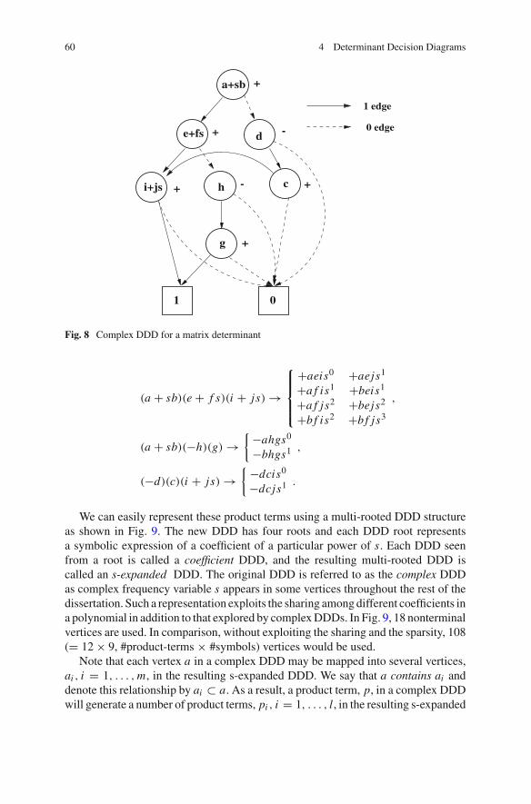
60 4 Determinant Decision Diagrams
0 edge
1 0
a+sb
e+fs d
h c
1 edge
i+js
g
+
+
+
-
+
+
-
Fig. 8 Complex DDD for a matrix determinant
(a + sb)(e + f s)(i + js) ⊕
⎧⎪⎪⎨
⎪⎪⎩
+aeis0 +aejs1
+a f is1 +beis1
+a f js2 +bejs2
+b f is2 +b f js3
,
(a + sb)(−h)(g) ⊕⎢−ahgs0
−bhgs1 ,
(−d)(c)(i + js) ⊕⎢ −dcis0
−dcjs1 .
We can easily represent these product terms using a multi-rooted DDD structureas shown in Fig. 9. The new DDD has four roots and each DDD root representsa symbolic expression of a coefficient of a particular power of s. Each DDD seenfrom a root is called a coefficient DDD, and the resulting multi-rooted DDD iscalled an s-expanded DDD. The original DDD is referred to as the complex DDDas complex frequency variable s appears in some vertices throughout the rest of thedissertation. Such a representation exploits the sharing among different coefficients ina polynomial in addition to that explored by complex DDDs. In Fig. 9, 18 nonterminalvertices are used. In comparison, without exploiting the sharing and the sparsity, 108(= 12 × 9, #product-terms × #symbols) vertices would be used.
Note that each vertex a in a complex DDD may be mapped into several vertices,ai , i = 1, . . . ,m, in the resulting s-expanded DDD. We say that a contains ai anddenote this relationship by ai ∗ a. As a result, a product term, p, in a complex DDDwill generate a number of product terms, pi , i = 1, . . . , l, in the resulting s-expanded
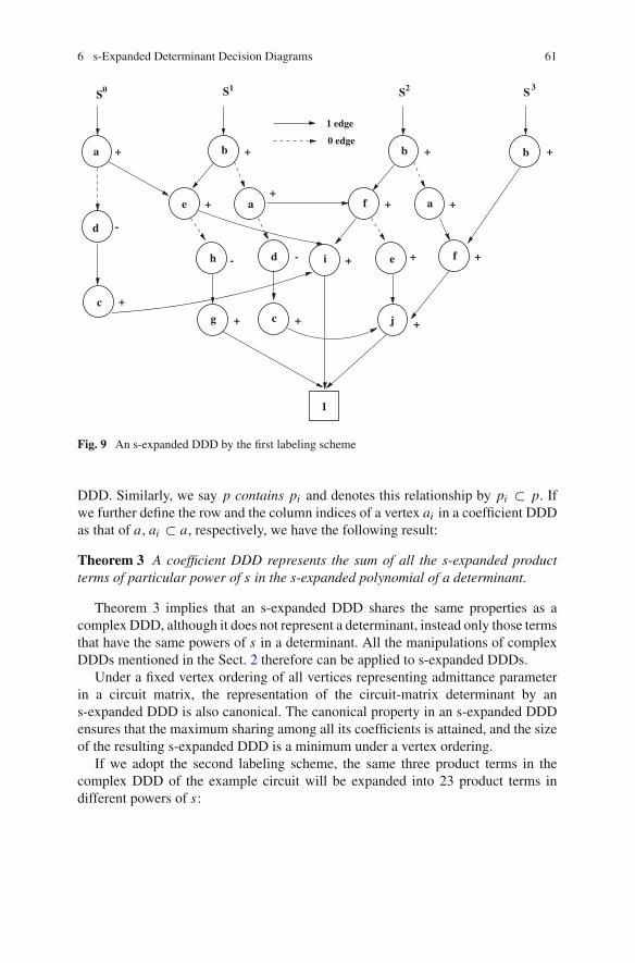
6 s-Expanded Determinant Decision Diagrams 61
0 edge
1 edge
S S S S
1
0 2 31
a
d
c
b
e a
h
g c
d i
f
b
a
f
b
j
e
+ +
+
+
+
+
+
+--
++
++
-
+
++
Fig. 9 An s-expanded DDD by the first labeling scheme
DDD. Similarly, we say p contains pi and denotes this relationship by pi ∗ p. Ifwe further define the row and the column indices of a vertex ai in a coefficient DDDas that of a, ai ∗ a, respectively, we have the following result:
Theorem 3 A coefficient DDD represents the sum of all the s-expanded productterms of particular power of s in the s-expanded polynomial of a determinant.
Theorem 3 implies that an s-expanded DDD shares the same properties as acomplex DDD, although it does not represent a determinant, instead only those termsthat have the same powers of s in a determinant. All the manipulations of complexDDDs mentioned in the Sect. 2 therefore can be applied to s-expanded DDDs.
Under a fixed vertex ordering of all vertices representing admittance parameterin a circuit matrix, the representation of the circuit-matrix determinant by ans-expanded DDD is also canonical. The canonical property in an s-expanded DDDensures that the maximum sharing among all its coefficients is attained, and the sizeof the resulting s-expanded DDD is a minimum under a vertex ordering.
If we adopt the second labeling scheme, the same three product terms in thecomplex DDD of the example circuit will be expanded into 23 product terms indifferent powers of s:

62 4 Determinant Decision Diagrams
0 edge
1 edge
1
0SS1S23S
c
h
a
c
a
f b
l
h
k
a
f b
e
de
d
gc
b h+
+ + +
+
-
+
+
+
_
+ +
++
+
+ +
+
++
+
i +
j _
+
g
Fig. 10 An s-expanded DDD by the second labeling scheme
(a + b + cs)( f + g + hs)(k + ls) ⊕
⎧⎪⎪⎪⎪⎨
⎪⎪⎪⎪⎩
+a f ks0 +bgls1 +agks0 +ahks1
+b f ks0 +bhks1 +bgks0 +ahls2
+c f ks1 +bhls2 +cgks1 +chks2
+a f ls1 +c f ls2 +agls1 +cgls2
+b f ls1 +chls3
,
(a + b + cs)(− j)(i) ⊕⎧⎨
⎩
−ajis0
−bjis0
−cjis1,
(−e)(d)(k + ls) ⊕⎢−edks0
−edls1 .
The resulting s-expanded DDD is depicted in Fig. 10. It is easy to see that thesecond labeling scheme results in more vertices than the first one. The resultings-expanded DDD has the same properties as the previous one (using the first labelingscheme), but it will be more suited for the DDD-based approximation to be presentedin Sect. 7.

6 s-Expanded Determinant Decision Diagrams 63
Fig. 11 The s-expanded DDDconstruction algorithm withthe first labeling scheme
CoeffConstruction(D)1 if ( D = 0 or D = 1)2 return NULL3 L0 = CoeffConstruction(D0)4 L1 = CoeffConstruction(D1)5 if (D.g = 0)6 Pg = CoeffMulplty(L1, D.g)7 if (D.c = 0)8 Pc = CoeffMulplty(L1 ∗ s,D.c)9 Presult = CoeffUnion(Pc, Pg)10 if (D.l = 0)11 Pl = CoeffMulplty(L1/s,D.l)12 Presult = CoeffUnion(Pl, Presult)13 return CoeffUnion(Presult, L0)
6.2 Construction of s-Expanded DDDs
6.2.1 The Construction Algorithm
An s-expanded DDD can be constructed from a complex DDD by one depth-firstsearch of the complex DDD. The procedure is very efficient with the time complexitylinear in the number of the resulting s-expanded DDD.
For convenience, we first present the construction algorithm using the first labelingscheme. Let D be a complex DDD vertex, with its 1-edge pointing to D1 and its0-edge pointing to D0. Let D.g, D.c and D.l denote, respectively, the admittance ofthe conductance, capacitance and inductance in the circuit. An s-expanded DDD, P ,is list of coefficient DDDs with P[i] denoting the coefficient DDD of power si andi ∗ [−n, n]. Then, we introduce the following four basic operations:
• CoeffUnion(P1, P2) computes the union of two s-expanded DDDs, P1 and P2.• CoeffMulplty(P, D.x) computes the product of s-expanded DDD P and coef-
ficient DDD vertex D.x .• P ∗ s increments the power of s in s-expanded DDD P .• P/s decrements the powers of s in s-expanded DDD P .
Algorithm CoeffConstruction described in Fig. 6.2.0 takes a complex DDDvertex and creates its corresponding coefficient DDDs. The implementations ofCoeffUnion and CoeffMulplty are also shown in Fig. 11 in terms of the basicDDD operations Multiply and Union, whose implementations can be found in theFig. 1.
As in all other DDD operations [196], we cache the result ofCoeffConstruction(D), and in case D is encountered again, and its result will be used directly.
In the second labeling scheme, we use D.xi to represent the i th admittance para-meter in a complex DDD vertex D. D.xi can be a resistive admittance, a capacitiveadmittance or an inductive admittance. The function t ype(D.xi ) will return res,cap and ind for the three admittance types, respectively. The CoeffConstructionusing the second labeling scheme is expressed in Fig. 12 (Fig. 13).

64 4 Determinant Decision Diagrams
Fig. 12 The basic algorithmsfor s-expanded DDD con-struction
CoeffMulplty(P,D.x)1 for i = −n to n do2 P [i] = Multiply(P [i], D.x)3 return P
CoeffUnion(P1, P2)1 for i = −n to n do2 P [i] = Union(P1[i], P2[i])3 return P
Fig. 13 The s-expanded DDDconstruction algorithm withthe second labeling scheme
CoeffConstruction(D)1 if ( D = 0 or D = 1)2 return NULL3 L0 = CoeffConstruction(D0)4 L1 = CoeffConstruction(D1)5 Presult = NULL6 for i = 1 to k do7 if (type(D.xi) = res)8 Pg = CoeffMulplty(L1,D.xi)9 Presult = CoeffUnion(Pg, Presult)10 if (type(D.xi) = cap)11 Pc = CoeffMulplty(L1 ∗ s,D.xi)12 Presult = CoeffUnion(Pc, Presult)13 if (type(D.xi) = ind)14 Pl = CoeffMulplty(L1/s,D.xi)15 Presult = CoeffUnion(Pl, Presult)16 return CoeffUnion(Presult, L0)
Consider a n × n circuit matrix. A complex DDD Dr with its size denoted by|Dr | is used to represent the determinant of the circuit matrix. Let n be the sizeof the determinant Dr represents. The maximum number of the circuit admittanceparameters in an entry of a circuit matrix is k. Then, we have the following result forthe s-expanded DDD derived from Dr by CoeffConstruction for both labelingschemes [197]:
Theorem 4 The time complexity of CoeffConstruction(Dr ) and the number ofvertices (size) of the resulting s-expanded DDD are O(kn|Dr |).Proof Function CoeffConstruction(Dr ) performs a depth-first search on Dr ,so it will visit each DDD vertex just once, and CoeffConstruction will be calledjust |Dr | times.
7 DDD-Based Symbolic Approximation
Deriving interpretable symbolic small-signal characteristics of analog integratedcircuits by approximation can build the circuit behavioral models and gain intuitiveinsights into the circuit behavior. In this section, we present one efficient algorithms

7 DDD-Based Symbolic Approximation 65
for obtaining approximate symbolic expressions based on DDD presentation ofsymbolic expressions. We show that a dominant term of a determinant can be foundby searching shortest paths in the DDD graphs in a linear time in terms of DDD graphsizes. Finding the k dominant product terms can be obtained by an incremental kshortest path search algorithm.
Before we generate the dominant terms, one problem we need to consider issymbolic cancellation. Symbolic canceling terms arise from the use of the MNAformulation in analog circuits. For instance, consider the s-expanded DDD in Fig. 9.Since g = k = 1
R3and i = j = − 1
R3, term agks0 cancels term −ajis0 in the coef-
ficient DDD of s0. Our experiments show that 70–90 % terms are canceling terms.Clearly it is inefficient to generate the 70–90 % terms that will not show up in thefinal expressions de-cancellation. It will be shown in [236] that fundamentally sym-bolic cancellation is caused by the submatrix reduction or variable/node reduction.MNA formulation is obtained by reducing all the branch current and branch voltagevariables from the sparse tableau formulation, which is cancellation-free [252]. Sucha reduction will lead to the symbolic cancellation [228]. More detailed treatment ofthis issue will be covered in [159, 227].
It turns out that symbolic canceling terms can be efficiently removed during [159]or after the s-expanded DDD construction [197]. In the following, we assume westart with the cancellation-free DDDs.
7.1 Finding Dominant Terms by Incremental k-Shortest PathAlgorithm
In the following, we present an efficient algorithm for finding k dominant termsin [237]. The algorithm does not require DDDs to satisfy certain graph theoreticalproperty required by the dynamic programming based method [248, 250] and thuscan be applicable to any DDD graph.
The SP algorithm is based on the observation that the most significant term incoefficient DDDs can be transformed into the shortest path in edge-weighted DDDgraphs by introducing the following edge weight in a DDD:
• 0-edge costs 0• 1-edge costs −log|ai |, and |ai | denotes the numerical value of the DDD vertex ai
that originates the corresponding 1-edge.
The weight of a path in a coefficient DDD is defined to be the total weights of theedges along the path from the root to the 1-terminal. As a result, given a path, sayabcde f , their path weight is
− (log|a| + log|b| + log|c| + log|d| + log|e| + log| f |). (9)
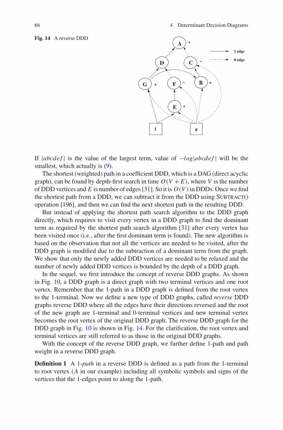
66 4 Determinant Decision Diagrams
Fig. 14 A reverse DDD
1
+
+ −
+
+
−
A
B
CD
F
E
G
0 edge
1 edge
0
If |abcde f | is the value of the largest term, value of −log|abcde f | will be thesmallest, which actually is (9).
The shortest (weighted) path in a coefficient DDD, which is a DAG (direct acyclicgraph), can be found by depth-first search in time O(V + E), where V is the numberof DDD vertices and E is number of edges [31]. So it is O(V ) in DDDs. Once we findthe shortest path from a DDD, we can subtract it from the DDD using Subtract()operation [196], and then we can find the next shortest path in the resulting DDD.
But instead of applying the shortest path search algorithm to the DDD graphdirectly, which requires to visit every vertex in a DDD graph to find the dominantterm as required by the shortest path search algorithm [31] after every vertex hasbeen visited once (i.e., after the first dominant term is found). The new algorithm isbased on the observation that not all the vertices are needed to be visited, after theDDD graph is modified due to the subtraction of a dominant term from the graph.We show that only the newly added DDD vertices are needed to be relaxed and thenumber of newly added DDD vertices is bounded by the depth of a DDD graph.
In the sequel, we first introduce the concept of reverse DDD graphs. As shownin Fig. 10, a DDD graph is a direct graph with two terminal vertices and one rootvertex. Remember that the 1-path in a DDD graph is defined from the root vertexto the 1-terminal. Now we define a new type of DDD graphs, called reverse DDDgraphs reverse DDD where all the edges have their directions reversed and the rootof the new graph are 1-terminal and 0-terminal vertices and new terminal vertexbecomes the root vertex of the original DDD graph. The reverse DDD graph for theDDD graph in Fig. 10 is shown in Fig. 14. For the clarification, the root vertex andterminal vertices are still referred to as those in the original DDD graphs.
With the concept of the reverse DDD graph, we further define 1-path and pathweight in a reverse DDD graph.
Definition 1 A 1-path in a reverse DDD is defined as a path from the 1-terminalto root vertex (A in our example) including all symbolic symbols and signs of thevertices that the 1-edges point to along the 1-path.

7 DDD-Based Symbolic Approximation 67
1 0
D
D’D’
0
D
1
(b)(a)
Fig. 15 Incremental k-shortest path algorithm
Definition 2 The weight of a path in a DDD is defined to be the total weights of theedges along the path where each 0-edge costs 0 and each 1-edge costs −log|ai |, and|ai | denotes the numerical value of the DDD vertex ai that the corresponding 1-edgepoints to.
We then have the following result.
Lemma 4.1 The most significant product (dominant) term in a symbolic determinantD corresponds to the minimum cost (shortest) path in the corresponding reverse DDDbetween the 1-terminal and the root vertex.
The shortest path in a reverse s-expanded DDD, which is still a DAG and thus,can be found in O(|DDD|) time as the normal DDD graph does.
Following the same strategy in [237], after we find the shortest path from a DDD,we can subtract it from the DDD using Subtract() DDD operation, and then wecan find the next shortest path in the resulting DDD. We have the following result:
Lemma 4.2 In a reverse DDD graph, after all the vertices have been visited (afterfinding the first shortest path), the next shortest path can be found by only visitingnewly added vertices created by the subtraction operation.
Figure 15 illustrates the incremental k-shortest path algorithm incremental k-shortest path algorithm. The figure in the left-hand side shows consecutive k-shortestpath algorithm to find the shortest path. Every time when a new DDD graph is createdwhich is rooted at D′, we have to visit the whole graph to find the shortest path. Thefigure shown in the right-hand side is the new incremental k-shortest path algorithmwhere we only need to visit all the newly created DDD nodes (in the upper lefttriangle) to be able to find the shortest path. As shortest paths are found from thesource to all the nodes in a graph, the shortest paths, shown in dashed lines, in theexisting subgraphs can be reused in the new DDD graph.

68 4 Determinant Decision Diagrams
FindNextShortestPath(D)1 if (D = 0)2 return 03 P = ExtractPath(D)4 if (P exists and P not equal to 1)5 D = SubtractAndRelax(D,P )6 return P
SubtractAndRelax(D,P )01 if (D = 0)02 return 003 if (P = 0)04 return D05 if (D = P )06 return 007 if (D.top > P.top)08 V = GetVertex(D.top, D.child1,
SubtractAndRelax(D.child0, P ))09 if (D.top < P.top)10 V = SubtractAndRelax(D,P.child0)11 if (D.top = P.top)12 T1 = SubtractAndRelax(D.child1, P.child1))13 T0 = SubtractAndRelax(D.child0, P.child0)14 V = GetVertex(D.top, T1, T0)15 if (V not equal to D)16 Relax(V.child1, V )17 Relax(V.child0, V )18 return V
Fig. 16 The algorithm for incremental k-shortest path based dominant term generation
It turns out that finding the shortest path from 1-terminal to the new verticescan be done very efficiently when those new vertices get created. The shortest pathsearching can virtually take no time during the subtraction operation. Suppose thatevery vertex in reverse DDD graph D has a shortest path from 1-terminal to it (bevisited once). Then the new algorithm for searching the next dominant term is givenin Fig. 16.
In FindNextShortestPath(D), ExtractPath(D) obtains the found shortestpath from D and returns the path in a single DDD graph form. This is done bysimply traversing from the root vertex to 1-terminal. Each vertex will remember itsimmediate parent who is on the shortest path to the vertex in a fully relaxed graph(relaxation concept will be explained soon). Once the shortest path is found, wesubtract it from the existing DDD graph and relax the newly created DDD vertices(line 15–17) at same time to find the shortest paths from 1-terminal to those ver-tices, which is performed in the modified function Subtract(D, P), now calledSubtractAndRelax(D, P).
In function SubtractAndRelax(D, P), Relax(P , Q) performs the relaxationoperation, an operation that checks if a path from a vertex’s parent is the shortestpath seen so far and remember the parent if it is, for vertices P and Q where P is the

7 DDD-Based Symbolic Approximation 69
Fig. 17 The Relax() routine Relax(P , Q)1 if d(Q) > d(P ) + w(P,Q)2 d(Q) = d(P ) + w(P,Q)3 parent(Q) = P
immediate parent of Q in the reverse DDD graph. The relaxation operation is shownin Fig. 17. Here, d(x) is the shortest path value see so far for vertex x ; w(P, Q) isthe weight of the edge from P to Q, which actually is the circuit parameter valuethat Q represents in the reverse DDD graph. Line parent (Q) = P remembers theparent of Q in the shortest path from the 1-terminal to Q. In the reverse DDD graph,each vertex has only two incoming edges (from its two children in the normal DDDgraph), so the relaxation with its two parents in lines 16 and 17 are sufficient for therelaxation of vertex V . Moreover, the relaxation for V happens after all its parentshave been relaxed due to the DFS-type traversal in SubtractAndRelax(). Thisis consistent with the ordering requirement of the shortest path search algorithm.Therefore by repeatedly invoking function FindNextShortestPath(D), we canfind all the dominant terms in a decreasing order.
Let n be the number of vertices in a path from 1-terminal to the root vertex, i.e.the depth of the DDD graph, given the fact that D is a DDD graph and P is a pathin the DDD form, then we have the following theorem:
Theorem 5 The number of new DDD vertices created in functionSubtractAndRelax(D, P) is bounded by n and the time complexity of the
function is O(n).
We then have the following result for incremental k-SP based algorithm:
Theorem 6 The time complexity of the incremental k-SP algorithm for finding kshortest paths is
O(|DDD| + n(k − 1)), (10)
where n is the depth of the DDD graph.
Notice that both DP based algorithm and incremental k-SP based algorithm havetime complexity O(|DDD|) to find a dominant term, where |DDD| is the size ofa DDD graph. After the first dominant term, however, both algorithms show bettertime complexities for generating next dominant terms, that is O(n). But in contrast toDP based algorithm, the actual running time of the incremental k-SP based algorithmdoes not depend on the topology of a circuit.
Notice that the new incremental k-shortest path generation algorithm can be per-formed on any DDD graph, including cancellation-free s-expanded DDD. We notethat the variant of DDD used by Verhaegen and Gielen in [248, 250] does not satisfythe canonical property due to vertex duplication. As a result, except for the first short-est path, remaining dominant paths cannot easily be generated by using the shortestpath algorithm as the found shortest path is hard to be subtracted (if possible at all)as most DDD graph operations are not valid for a non-canonical DDD graph.

70 4 Determinant Decision Diagrams
Following the same strategy in [258], our approach also handles numericalcancellation. Since numerical canceling terms are extracted one after another, theycan be eliminated by examining two consecutive terms.
8 Summary
In this chapter, we briefly review the determinant decision diagram (DDD) conceptsand its application for symbolic analysis and generating the dominant symbolic termsfor analog behavioral modeling. We start with the basic concept of a DDD, its mainproperties and manipulative operations for symbolic analysis. Then we introduce anefficient DDD construction algorithms by logic synthesis and operation. We thenpresent s-expanded DDDs to represent s-expanded polynomials and s-domain trans-fer functions. Finally we give a shortest-path-searching based algorithm for findingk dominant symbolic terms for symbolic approximations. The new algorithm has alinear time complexity in terms of DDD graphs and can find k dominant terms veryefficiently.
This chapters cover all the basic essence about DDD-based symbolic analysis.We do not include many proof details and numerical results. Interesting readers canrefer to more detailed treatment of DDD graphs and application in [159, 227].

Chapter 5DDD Implementation
1 Introduction
In this chapter we mainly discuss the issues involved with the implementation ofDeterminant Decision Diagram and an investigation on its complexity. It turns out thatthe performance of a DDD implementation is mainly determined by several factorsthat interact to each other; the key factors among them are how the matrix elementsare ordered and how a hash table is designed. A variable order determines the ultimateDDD size while the hash table design determines the efficiency during the course ofconstruction. Working together, these two components determine dominantly howmuch time and memory are consumed by one construction cycle. One may easilycreate some benchmark problems which can be solved by some implementationswhile not by some other implementations because of the limited memory on a givencomputer.
When BDD is applied to a specific problem field other than logic functions, a goodimplementation often requires a proper understanding of the underlying problemnature. Determinant is a relatively easy-to-describe mathematical object, the com-plexity of whose expansion is mainly determined by its sparsity pattern. Althoughan optimal element order for an arbitrary matrix is unknown in most cases, somegeneric knowledge on the sparsity like the row/column degrees can be helpful fordeveloping ordering heuristics.
Regarding the hash table design, we have already pointed out in Chap. 3 that eithertriple-based or object-based hashing mechanism can be used for hashing. For deter-minants, both hash schemes can be used in implementation. Since the determinantexpansion generates a set of product terms, i.e., a sum-of-product system, its analogyto logic expressions reminds us to use a logic-BDD-based approach (i.e., triple-basedhash) for DDD construction [196, 230]. However, further investigation and exper-imental implementations have revealed that the efficiency of using a logic-basedimplementation is not necessarily the best.
We shall establish a basic property in this chapter that, given a pre-chosen order-ing of the matrix elements, any minor can be uniquely identified by its row and
G. Shi et al., Advanced Symbolic Analysis for VLSI Systems, 71DOI: 10.1007/978-1-4939-1103-5_5,© Springer Science+Business Media New York 2014

72 5 DDD Implementation
Table 1 Four types ofBDD-based implementations
Hash (good) Hash (bad)
Order (good) I IIOrder (bad) III IV
column indexes without the need of checking its entries. This property can be used forobject-bashed hashing in implementation and it has been justified that an implemen-tation based on this strategy could outperform a logic-BDD based implementation,if both implementations use the same ordering.
The above discussion also leads to a question on how to fairly compare twoimplementations of a BDD application. Because several interacting components areinvolved in an implementation, one cannot attribute the good performance of animplementation to one specific technique. Usually, several well-designed softwarecomponents work together to arrive at a good performance. Even so, because theperformance of BDD is so sensitive to variable ordering, an implementation has tomake sure that the performance is relatively stable for different set of problems byusing the implemented ordering heuristic.
We shall also make it clear in this chapter that sometimes an ordering scheme mightrestrict an implementation strategy; that is, choosing an implementation might haveimplicitly chosen a variable order. For example, as we shall present in this chapter,a DDD can be implemented simply by expanding a determinant always following arow (or column) of any minor generated in the middle. Then, such a program cannotbe used to test-run an arbitrary element order.
In practice, a performance comparison between two DDD implementations shouldreflect the overall contributions of the ordering and hash strategies adopted. Table 1classifies four types of implementations for performance evaluation. In general, animplementation with both a good hash method and a good ordering scheme shouldhave a satisfactory performance.
2 Early Versions of DDD Implementation
The first proposal of DDD performs the following steps for symbolic construction[196]:Early Version of DDD Construction Flow:
Step 1. Parse a circuit to an internal representation in modified nodal analysisformulation.
Step 2. Expand the coefficient determinant once by using an indexing algorithmcalled Greedy-Labeling to assign each matrix element an index.
Step 3. Expand the determinant again in the indexed order to construct a DDD.Step 4. Scan the DDD to determine the vertex signs.Step 5. Evaluate DDD to perform AC analysis.

2 Early Versions of DDD Implementation 73
Several points in the steps are explained here: In Step 2 the Greedy-Labeling algorithmproposed in [196] makes use of row and column degrees for ordering. A row (resp.column) degree is defined to be the count of nonzero in the row (resp. column). Arow with the minimum degree is called the min-degree (short for minimum degree)row; likewise for column. For each intermediately generated minor, the Greedy-Labeling algorithm would choose an element with the minimum degree. Supposea min-degree row is selected, then the elements in that row are sorted according totheir increasing column degrees and this order is followed in the later expansions.After the expansion is completed, a bottom-up recursion indexes the elements. Anyalready indexed elements encountered again in the recursion are skipped.
It is clear that this procedure runs two expansions separately, one for indexing andthe other for building DDD. This design by two-round expansions can be improved.
We know in determinant expansion that when an element is selected, its cofactorsign can be determined immediately by its row and column location (r, c) in the minor,i.e., (−1)r+c. However, the procedure described above does not directly make use ofthis property. The main reason is because of the hash scheme used. By using a triple-based hash scheme, the minor structures are not preserved, hence, the row-columninformation cannot be used. For this reason, the extra Step 4 is required to determinethe vertex signs (i.e., the cofactor signs). Again, this step can be removed by usinganother hash scheme.
The core step of the stated procedure is Step 3 by which a DDD data structureis constructed. This step consumes most of the time and memory. Hence, a carefuldesign of the details is considered important. The work [196] made use of a third-party BDD package implemented for the set manipulation of a subset system. Minato[134] introduced a notion called Zero-suppressed BDD (ZBDD) to reduce a BDDwhen there are solid arrows pointing to the zero-terminal. He also defined a set ofroutines for subset operations, such as Change() to switch the two children objectspointed by two decision arrows, and Union() to merge two subsets. These routinescan be employed for composing the determinant product terms from bottom-up forthe DDD construction. A vertex-triple based hash is at the center of the construction.
One should be aware that the above procedure is an exhaustive enumeration ofall product terms, which is a direct bottom-up construction by successively applyingalgebraic operations to lower-dimensional cofactors until the full-dimensional deter-minant is computed. Although the resulting DDD is shared, the construction cycleis time-consuming. Hence, one should not directly use such a construction method.One technique to avoid exhaustive expansion is to incorporate a minor-based cacheto improve the time efficiency, which was employed in the work [196]. While inconstruction, the minor indexes are temporarily saved in a cache table for lookupin the later steps. Because the entries in a cache are erasable upon a collision, thestorage is not permanent; hence, minor re-expansions happen often. It is obvious thatthe re-expansions caused by hash-miss waste quite an amount of construction time.
In another work [230], the Step 3 of the procedure was replaced by a logic synthesisprocedure, by which all product terms of a determinant are equivalently described bya disjunction of conjunctive logic encodings of the row-column combinations. Thecombinational logic expressions are then synthesized by a third-party logic BDD

74 5 DDD Implementation
package to create a DDD. Again, this method uses triple-based hash; hence, minorre-expansion still exists. On the other hand, the cofactor signs have to be determinedas in the first method by another scan of the finished DDD.
3 Minor Hash Function
The first version of DDD implementation flow can be improved and simplified bydeveloping new expansion and hash strategies. One simple method is to expandminors by always following a selected row (or column). The selection of row orcolumn is on-the-fly according to the min-degree of the current minor. With thismethod a pre-ordering phase becomes unnecessary. During expansion hash is basedon the minors. By preserving the minor indexes in the hash table, the cofactor signscan be determined simply. In this sense, Step 4 in the traditional flow also becomesunnecessary.
Moreover, the new hash mechanism uses only the row and column indexes of aminor (called minor indexes) for hashing. As a result, only one Minor Hash Tableis sufficient for DDD construction; no cache table is needed. It is not necessary touse a third-party BDD package anymore. Experiments have verified that the sim-plifications as made above can greatly improve the runtime efficiency of the DDDimplementation.
The Laplace expansion of a determinant det(A) along the i th row can be written as
det(A) =n∑
j=1
(−1)i+ j ai, j Mi, j , (1)
where ai, j is the (i, j)th element of matrix A and Mi, j denotes the minor of matrixA by deleting the i th row and j th column. Since each Mi, j is a minor of one lessdimension, it can be further expanded by selecting another row or column.
In DDD, each vertex is defined by a symbol (i.e., a matrix element) and a minorgenerated by the preceding operations. For example, the root vertex is defined bythe first matrix element and the original determinant. At each nonterminal vertex,one of the operations, “Minor” or “Rem” (short for “Remainder”), is applied to theassociated minor by selecting another nonzero element from the minor according toa specific order. Before the next expansion is performed, we must check whether thecurrent minor has already been expanded once. On this occasion we look up fromthe minor hash table.
The next theorem ensures that we only need to use the indexes of a minor toidentify a minor without the necessity of comparing the entries.
Theorem 5.1 ([199]) Let the symbol order be fixed for a determinant. If two minorsassociated with two DDD vertices have the same symbol name and the minors havethe identical row and column indexes, then the two minors must be identical; namely,their entries are exactly equal.

3 Minor Hash Function 75
Note that if two minors of the same row-column indexes are generated by applyingtwo random sequences of “Minor” and “Remainder” operations independently, thenit is not guaranteed that the minor entries would match each other. Hence, the con-dition of “fixed symbol order” in the theorem is essential.
proof (This proof was first presented in [199].) The proof is based on a fixed symbolorder. For simplicity we consider the following two 3 × 3 minors M1 and M2,
M1 =∣∣∣∣∣∣
× α ×β × ×× 0 0
∣∣∣∣∣∣, M2 =
∣∣∣∣∣∣
× 0 ×β × ×× 0 0
∣∣∣∣∣∣, (2)
where α, β, and × indicate the nonzero elements remaining. Suppose the two minorshave identical row and column indexes, and are associated with two DDD verticesnamed by the same symbol β. If the two minors are not identical, then they musthave at least one entry different from each other. Let it be α in minor M1. Then thecorresponding entry in minor M2 must be zero because of a “Remainder” operationapplied earlier. This would imply that the symbol α precedes β in the symbol order.But in the minor M1 symbol α is still there, i.e., not processed yet. The abovehypothesis has led to a contradiction. �
Theorem 5.1 is simple but highly useful for designing a minor-based hash mecha-nism for DDD construction. Comparing the indexes of a k × k minor only requires acomparison of 2k integer numbers, while a “deep” comparison of two minors wouldhave to compare all k2 entries in the worst case.
The row and column indexes of a minor can be saved in a hash table calledMinor Hash Table. This table is not only used for looking up identical (shareable)minors, but also used for determining the cofactor signs, because whenever an entryis selected from a minor, its relative row-column position is known. Owing to theuniqueness established by Theorem 5.1, no identical minor will be expanded twice.It would save quite an amount of construction time in practice.
In the next section we describe a layered determinant expansion method for DDDconstruction [200]. This method applies a row/column-based ordering and minor-based hash; hence, it is very easy to understand and implement.
4 Layered Expansion of Determinant
The layered expansion of a determinant is very intuitive; it can be illustrated by anexample. We shall expand the following 3 × 3 determinant
A =∣∣∣∣∣∣
a b cd e fg h i
∣∣∣∣∣∣
(3)

76 5 DDD Implementation
i
0i
1
0
0
0
0
0
0
(a) (b)
Fig. 1 a LED of the 3 × 3 full matrix. b Converted DDD
in a rowwise expansion order. When working on the first row {a,b, c}, we create aqueue to save all elements in that row. The queue is shown as the first (top) layer inFig. 1a. Then we go to the queue head and start processing the elements one by onein the queue.
Let us work on the first element ‘a’ by deleting its row and column (called cofac-toring). It results in a reduced minor
Ma =∣∣∣∣e fh i
∣∣∣∣ . (4)
This minor will be further expanded by its first row {e, f }. Before doing that, wesave these elements in another queue, which is shown as the second layer in Fig. 1a.We continue on to the elements ‘b’ and ‘c’ remaining in the first queue in the samemanner.
Expanding the second element ‘b’ in the first queue results in the next reducedminor
Mb =∣∣∣∣d fg i
∣∣∣∣ . (5)
Still this minor will be expanded by its first row {d, f }, and the elements are saved inthe second queue as well following the existing elements, see Fig. 1a. Likewise, wedo a similar expansion for the element ‘c’ and the second queue is further appendedwith {d, e}.
There are three segments in the second queue, each containing one row of elementsfrom a reduced minor. Because each segment is a result of expanding one element inthe first queue, it is marked by an arrow from the element in the preceding layer, asshown in Fig. 1a. For example, looking at the queue in the second layer in Fig. 1a, thefirst two elements {e, f } form a segment by expanding element ‘a’ in the previouslayer. Hence, the relationship is indicated by connecting an arrow from ‘a’ to ‘e’.The elements in a segment are called sibling elements and the first element in onesegment is called the segment head.

4 Layered Expansion of Determinant 77
Since each segment in the second layer is a row from a 2 × 2 minor, each elementin one segment should be expanded further to get 1 × 1 minors. The resulting 1 × 1minors will be saved in another queue in the third layer. When we are working onthis step of expansions, we run into the possibility of “sharing”, because expandingthe three 2 × 2 minors with the second layer would result in six 1 × 1 minors, butonly three of them are different, which are ‘i’, ‘g’, and ‘h’ shown in the third layerof Fig. 1a, each element is shared by two arrows from the second layer.
The layered expansion process is summarized as follows: Create a queue for eachlayer, which is used for saving the equal-dimensional rows or columns selected forfurther expansion. The elements saved in the queue in each layer are segmented, eachbeing a row or a column. To make the expansion traceable, we create links from anelement in a preceding layer to a segment head in the next layer, which is called asegment pointer. We always scan the elements from the head of a queue toward thetail, and successively append the element segments in the next queue. Repeat thisprocess until the bottommost queue is filled with 1×1 minors. A diagram constructedthis way is called a Layered Expansion Diagram (LED).
Several properties of LED are stated below. They are useful for implementation.
Property 5.1 The elements in any segment share the same minor.
For example, the elements {a,b, c} in the first layer of Fig. 1a form a segment. Theyare from the same minor which is the original determinant A. We shall be using therow and column indexes to denote a minor by a notation like M{(1, 2, 3); (1, 2, 3)},where the first array (1, 2, 3) lists the row indexes and the second array (1, 2, 3)
lists the column indexes. Hence, M{(1, 2, 3); (1, 2, 3)} denotes the determinant A.Because all elements in a segment share one minor, in implementation it suffices tokeep only one minor for all the elements in a segment. The minor row and columnindexes as two arrays are saved in a minor hash table. Whenever a minor is to beexpanded, it is first looked up from the hash table. If it is found, this current minordoes not have to be re-expanded. Otherwise, the minor is saved to the hash table.
The sharing in an LED is created by this hash mechanism. For example, theelement ‘i’ in the bottom queue in Fig. 1a is shared. So are elements ‘h’ and ‘g’. Theabove discussion leads to the second property of LED.
Property 5.2 The minors associated with the elements in the same queue of an LEDare of equal dimension. The minor dimensions always decrease by one from one layerto the next. For an n × n determinant, there must be n layers in an LED unless thedeterminant is singular.
Although sharing has been enforced in the LED construction, an LED as con-structed above is not a BDD (hence DDD) yet. But converting an LED to a BDD isstraightforward as we shall see below. After being converted to a DDD, it becomesmuch easier to manipulate the data structure for symbolic analysis. Hence, followingthe first phase of LED creation, the second phase of the LED-based method is toconvert an LED to a DDD.
The conversion from an LED to a DDD is fairly straightforward. All the existingsegment pointers in an LED become the solid-arrows in DDD, standing for the Minor

78 5 DDD Implementation
operations. In addition, add dashed arrows successively between the elements in eachsegment, which stand for the Remainder operations. Terminate the last element ofeach segment by a dashed arrow at the terminal vertex zero. Finally, terminate allthe elements in the bottom queue by solid arrows at the terminal vertex one. Afteradding all the necessary arrows, we obtained a completed DDD, with the root beingthe first element in the top-layer queue.
A direct consequence of the conversion process described above leads to the thirdproperty of LED.
Property 5.3 The total number of elements in all queues in a LED (counting therepeated elements) is equal to the size of DDD, denoted by |DDD| (excluding thetwo terminal vertices).
5 LED Implementation
The LED construction procedure as described above is greatly different from thefirst version of DDD construction procedure. Specifically, the LED procedure hasthe following advantages.Advantages of LED:
1. It does not need a predefined explicit element order;2. It does not use any third-party BDD package; and3. It does not need to determine the cofactor signs in an separate phase.
5.1 Expansion Order in LED
We shall discuss a little more on the issue of element ordering. Instead of definingan a priori variable order as in the first DDD work [196], the LED method expandsa determinant by following dynamically selected rows or columns. Since any minorgenerated during expansion can be expanded by a row or column owned by theminor itself, the resulting 1-paths in the converted DDD might have some elementsnot following a fixed order.
The next example shows that an expansion order used in the LED construction isa slightly different notion from a pre-defined order for all matrix elements. In fact,the notion of expansion order is weaker than a sequential element order. Considerexpanding the following determinant
∣∣∣∣∣∣∣∣
a 0 0 b0 e f 00 g h 0c 0 0 d
∣∣∣∣∣∣∣∣
. (6)
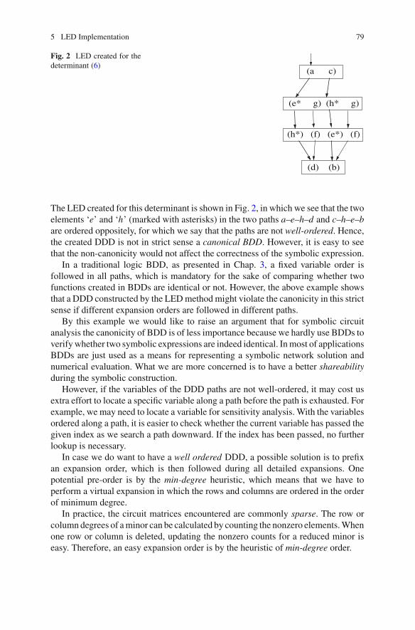
5 LED Implementation 79
Fig. 2 LED created for thedeterminant (6)
(h*) (f) (e*) (f)
(a c)
(d) (b)
(e* g) (h* g)
The LED created for this determinant is shown in Fig. 2, in which we see that the twoelements ‘e’ and ‘h’ (marked with asterisks) in the two paths a–e–h–d and c–h–e–bare ordered oppositely, for which we say that the paths are not well-ordered. Hence,the created DDD is not in strict sense a canonical BDD. However, it is easy to seethat the non-canonicity would not affect the correctness of the symbolic expression.
In a traditional logic BDD, as presented in Chap. 3, a fixed variable order isfollowed in all paths, which is mandatory for the sake of comparing whether twofunctions created in BDDs are identical or not. However, the above example showsthat a DDD constructed by the LED method might violate the canonicity in this strictsense if different expansion orders are followed in different paths.
By this example we would like to raise an argument that for symbolic circuitanalysis the canonicity of BDD is of less importance because we hardly use BDDs toverify whether two symbolic expressions are indeed identical. In most of applicationsBDDs are just used as a means for representing a symbolic network solution andnumerical evaluation. What we are more concerned is to have a better shareabilityduring the symbolic construction.
However, if the variables of the DDD paths are not well-ordered, it may cost usextra effort to locate a specific variable along a path before the path is exhausted. Forexample, we may need to locate a variable for sensitivity analysis. With the variablesordered along a path, it is easier to check whether the current variable has passed thegiven index as we search a path downward. If the index has been passed, no furtherlookup is necessary.
In case we do want to have a well ordered DDD, a possible solution is to prefixan expansion order, which is then followed during all detailed expansions. Onepotential pre-order is by the min-degree heuristic, which means that we have toperform a virtual expansion in which the rows and columns are ordered in the orderof minimum degree.
In practice, the circuit matrices encountered are commonly sparse. The row orcolumn degrees of a minor can be calculated by counting the nonzero elements. Whenone row or column is deleted, updating the nonzero counts for a reduced minor iseasy. Therefore, an easy expansion order is by the heuristic of min-degree order.

80 5 DDD Implementation
5.2 Hash in LED
Next, we discuss another property with LED. Since the determinant expansion ofLED is always row/column-based, we wonder whether it is necessary to order theelements rowwise or columnwise to create a smaller DDD. The next property of LEDjust claims that it is immaterial to choose an in-row or in-column element order.
Property 5.4 The expansion order of the elements in any element segment isimmaterial in that the DDD size does not change by re-ordering the elements inany segment.
proof Looking at the LED given in Fig. 1a, we see that shuffling the elements in asegment in any queue would only change the element positions in their own queueand the enqueueing order of the segments in following layers. In other words, ahorizontal shuffling of the element order inside a segment only permutes the relevantelements and the connected arrows horizontally, which does not increase or decreasethe number of elements in each queue. Hence, the DDD size must not change. �
Since the segments and the number of elements in each segment are known at thetime of expansion, the element segments in any queue can be managed by assigningthe number of elements in segment to the head element. The head element in the topqueue, which has only one segment, is pointed by a root pointer.
In the sequel, by an expansion order of LED we always refer to the sequence ofrows and columns selected for expansion as we step from one layer to the next. ByProperty 5.4, what we shall do in implementation is to simply expand the elementsin one row or column in their natural order.
In light of the notion of expansion order, we have the following theorem as thebasis for minor hash in LED.
Theorem 5.2 If two expansion orders result in two minors of the same row andcolumn indexes, the two reduced minors must be identical.
proof The proof is straightforward. By following an expansion order, we alwaysdelete an entire row or column as we step from one layer to the next in LED. When areduced minor is generated, none of its entries should have been altered by the previ-ous row/column deletions. Hence, if two minors generated have identical row/columnindexes, they must have identical entries. �
Note that this theorem is slightly different from that stated in Theorem 1, wherea fixed element order is a prerequisite.
It is worth noting that in the LED construction, the Remainder operation ona determinant becomes implicit in the sense that we do not explicitly replace anelement by a zero. Because we know that the elements in a selected row or columnare expanded successively, it is not necessary to save such minors as the result ofRemainder operations.

5 LED Implementation 81
This fact simplifies the design of hash table. When expanding any element from aselected row or column, the working minor that includes the selected row or columncan be referenced to generate a new reduced minor. Hence, only the working minorhas to be saved in the Minor Hash Table while all the elements in a segment are beingexpanded. This fact was actually stated in Property 5.1.
Because a segment of elements can be traced by its head, it is only necessary tocreate a link (or an association) between a minor in the Minor Hash Table and thehead element of a segment. Whenever a minor is hashed, the linked head element isreturned for sharing, which creates the inter-layer arrows in an LED.
Suppose we use the min-degree heuristic for expansion. The following exampletells us how to manage a Minor Hash Table so that the update of row/column degreescan be simplified.
Let M{(2, 4, 6, 8); (1, 3, 5, 7)} denote the 4 × 4 minor obtained in a middle step
∣∣∣∣∣∣∣∣
0 a b 0c d 0 e0 0 f gh 0 0 i
∣∣∣∣∣∣∣∣
. (7)
The row and column degrees are respectively (2, 3, 2, 2) and (2, 2, 2, 3). Let theelement ‘a’ be selected for expansion. After deleting the first row and the secondcolumn in this minor, the resulting minor is denoted by M{(4, 6, 8); (1, 5, 7)} whichrepresents the reduced minor ∣
∣∣∣∣∣
c 0 e0 f gh 0 i
∣∣∣∣∣∣. (8)
The row and column degrees are respectively (2, 2, 2) and (2, 1, 3), which are notobtained by counting the nonzeros in the reduced minor, but deduced from the degreesgiven with the 4×4 minor by subtracting the nonzeros in the deleted row and column.
Keeping the minor indexes in the Minor Hash Table also simplifies determiningthe cofactor signs. For example, the sign of element ‘a’ in the 4 × 4 minor in (7)is determined by its relative row and column positions in the minor, which gives(−1)1+2.
On the other hand, saving the row/column degrees with a minor hash object alsosimplifies identifying a singular minor. A minor having one zero-degree row orcolumn must be singular. Whenever a singular minor is encountered, the currentsegment pointer in LED is terminated at NULL. Later, when a LED is converted to aDDD, all NULL pointers are replaced by solid arrows terminating at the zero vertex.Those vertices terminated by solid arrows to zero will be zero-suppressed later.

82 5 DDD Implementation
5.3 The LED Construction Procedure
The following pseudo-code summarizes the LED construction procedure.
Input: A determinant.Output: A Layered Expansion Diagram (LED).
01 Create queue Q(0) and enqueue a selectedrow or column to Q(0); k := 0;
02 While (true), do03 While (Dequeue element x in Q(k)), do04 Expand the minor at x ;05 Hash the reduced minor;06 If (Not hashed)07 Enqueue elements to Q(k + 1);08 End of while;09 If (Q(k + 1) is nonempty)10 k := k + 1; continue;11 Else12 Quit the loop;13 End of while;
In line 04, if the reduced minor is detected singular, then the element x is pointedto NULL, which indicates that no further expansion is necessary. In line 05, if thereduced minor is hashed, the segment head element linked to the saved minor in thehash table is returned for creating connection (i.e., sharing) from the element x tothe returned element. In line 07, the enqueued elements are from a row or columnselected for the next expansion. A recommended heuristic for the selection is by themin-degree heuristic. In line 11, if no elements are enqueued in the next queue, itsimply implies that the expansion has finished. In case Q(k) is empty for k < n−1, itjust means that the original determinant is symbolically singular; that is, after deletinga portion of rows and columns, the reduced matrix becomes a zero matrix.
6 Examples
Some experimental results on the performance of the LED algorithm have beenreported in the work [200]. We cite in this section some experimental data to illustratethe effectiveness of the LED algorithm and make a comparison on the orderingschemes.
The LED algorithm for DDD construction is very easy to implement. It wasimplemented by a C++ program in [200]. For the purpose of comparison, We alsoimplemented a traditional DDD program which allows pre-ordering the matrix ele-ments. To differentiate, we refer the former program by the LED-Program and thelatter by the DDD-Program. Both programs have the netlist parsing interface thatcan parse a small-signal netlist to build MNA matrices for ac analysis.

6 Examples 83
Table 2 Comparison of the DDD sizes constructed by LED and DDD with Greedy-Labeling forfull matrices
Matrix size 2 3 4 5 6
|DDD| (LED) 4 12 32 80 192|DDD| (Greedy) 4 13 40 118 340
7 8 9 10 11|DDD| (LED) 448 1,024 2,304 5,120 11,264|DDD| (Greedy) 965 2,708 7,535 20,828 57,266
12 13 14 15 16|DDD| (LED) 24,576 53,248 114,688 245,760 524,288|DDD| (Greedy) 156,764 427,571 1,162,580 3,152,681 8,529,668
17 18|DDD| (LED) 1,114,112 2,359,296|DDD| (Greedy) 23,030,492 62,072,002
We should mention the compiler and machine used for evaluation of the softwareimplementation. In the reported experiments, the C++ programs were compiled bygcc 3.4.4 installed with the Cygwin [32] (a Linux emulator on Windows). The com-puter was an Intel Duo 2.26GHz CPU installed with Windows XP and having 2GBmemory (with about 1G available for application programs.)
Since the Greedy-Labeling algorithm was reported to be the best ordering heuristicin [196], we collected the test-run results of the DDD-Program by using Greedy-Labeling for matrix element ordering. We did not implement a purely triple-basedhashing using a third-party BDD package in this investigation. Both programs imple-mented minor-based hash tables. Also for the purpose of investigation, both programswere implemented in a way that either matrix or circuit netlist can be an input. Thecorrectness of the computation results were verified by several measures, like thecalculated determinant values or the known number of terms if the input is a matrix,and the ac analysis results checked by HSPICE simulation if the input is a netlist.
6.1 Test on Full Matrices
The first part of performance test was made on a set of full matrices with all elementsnonzero. Full matrices are special in that an optimal order of matrix elements forDDD construction is known [199]. We shall discuss this issue in a later section. Fornow, we just mention that a natural row (or column) order is an optimal order for fullmatrices.
Table 2 shows the sizes of the DDDs created by the LED-program using thenatural rowwise order and by the DDD-Program using the Greedy order. Here, theDDD size (denoted by |DDD|) is defined to be the total count of DDD vertices minus2, excluding the two terminal vertices one and zero. The Greedy ordering employed

84 5 DDD Implementation
2 4 6 8 10 12 14 16 1810
0
101
102
103
104
105
106
107
108
Size of full matrix
Siz
e of
DD
D
|DDD| Greedy|DDD| Row order
Fig. 3 Comparison of the DDD sizes created by LED and DDD with a Greedy order for fullmatrices. The y-axis is plotted in log10-scale
by the DDD-Program produces different element orders from row/column ordering.For example, the order for the 3 × 3 full matrix created by the Greedy-Labelingalgorithm looks like [196]
∣∣∣∣∣∣
a(1) d(4) g(5)
b(2) e(6) h(8)
c(3) f (7) i (9)
∣∣∣∣∣∣. (9)
In Table 2 we see the DDD sizes created by the two programs increase expo-nentially with the matrix size, but with very different rates. When the matrix sizebecomes 18 × 18, the DDD size created by the Greedy order exceeds 30 times ofthe size by the LED-program, which is a huge difference. It means that, on the com-puter we used for test-run we could continue to run the LED-program for larger fullmatrices but the DDD-Program would fail for the 19 × 19 because of insufficientmemory.
The data given in Table 2 are visualized in Fig. 3, from which we can see clearlythe exponential growth rates of the DDD sizes. The plot hints us the following:The element order with the DDD construction is very important. Although using BDDcould not drastically change an exponential complexity problem to non-exponential,a proper ordering scheme does reduce the exponential growth rate.
In Sect. 7 we shall prove that the rowwise order for full matrices of dimension nis an optimal order and the optimal DDD size is (n · 2n−1) [199]. The DDD sizescreated by the LED-program in Table 2 are exactly predicted by this complexity.

6 Examples 85
Table 3 CPU time by the LED-program for full matrices
Matrix size 12 13 14 15 16 17 18
CPU time (s) 0.4 0.6 1.3 3.0 6.9 21.0 88
Besides the DDD sizes, the CPU time of running the LED-program is also areflection of the performance of implementation. On the computer we used for test-runs, the CPU time of running the LED-program for the full matrices larger than12 × 12 are collected in Table 3.
6.2 Test on Analog Circuits
We also tested the two programs on three operational amplifier circuits. Before pre-senting the test-run results, we make a brief introduction of a new matrix-basedformulation for symbolic analysis so that only one matrix has to be expanded toderive a symbolic network function, instead of expanding two matrices as requiredby using the Cramer’s rule.
Suppose a dc reference point has been simulated. Then substituting small-signalmodels to all transistors, a linear network results which can be represented by a setof linear equations Ax = b, where b is the input vector, x is the unknown vector,and A is the coefficient matrix. A well-conditioned circuit has a nonsingular matrixA so that the unknown is solved as x = A−1b.
Suppose the input is a nodal voltage referenced to the ground and the output isanother nodal voltage referenced to the ground. Let xu and xv be respectively thevariables corresponding to the input and the output. Then we have xu = eT
u A−1band xv = eT
v A−1b, where ek denotes the kth unit basis vector in the n-dimensionalEuclidean space. Let H be the input–output transfer function. Then the input–outputrelation becomes xv = H xu . After substituting the unit basis vectors, we get analternative expression eT
v A−1b = HeTu A−1b. It is easy to verify that this equation is
equivalent to the following equation in determinant form:
∣∣∣∣
A beTv − HeT
u 0
∣∣∣∣ = 0. (10)
By viewing the input–output transfer function H as a symbol (called an I/O symbol),the product terms resulting from expanding the determinant in (10) can be separatedinto two groups; one containing the symbol H , the other not. In other words, weshall get the following equation from the equation in (10):
D · (−H) + N = 0, (11)

86 5 DDD Implementation
Table 4 Comparison of CPU time and DDD sizes
Circuit #T1 N2 LED Greedyτ3 # Terms|DDD| CPU4 |DDD| CPU4
Opamp 1 22 (M) 15 2,507 0.2 s 1,178 0.5 s 2.99e + 4μA741 20 (Q) 25 13,722 0.6 s 19,572 6.6 s 4.20e + 06μA725 26 (Q) 34 115,590 5.4 s 38,997 8.1 s 1.28e + 081 Number of transistors with M standing for MOS and Q for bipolar2 Dimension of MNA matrix augmented by one dimension3 The I/O symbol is ordered first4 CPU time including DDD construction and ac analysis for ten points
where D denotes the sum of all terms by factoring out all (−H) and N the rest ofthe terms. Then the transfer function can be obtained by the expression H = N/D.
The above formulation method can be extended easily to other input-output (volt-age or current) variables. The coefficient matrix in (10) can be created easily inimplementation by an extended MNA stamping method. Note that the matrices soformulated have increased dimension by one or two.
In the scenario of symbolic analysis, we choose to place the unknown symbol Hthe foremost in implementation. For the LED-program, it means to expand the rowcontaining the symbol H first. When applying the Greedy ordering algorithm, weremove the unknown symbol H first from the matrix and run the Greedy-Labelingroutine on the remaining MNA matrix elements. After the rest of elements are orderedwith indexes, the symbol H is placed back with the first symbol index.
To differentiate, we refer to the slightly modified Greedy algorithm used in theDDD-Program as Greedyτ. We observed in experiment that the slight modificationto the Greedy ordering could likely change the DDD sizes drastically, with the reasonunknown.
The three benchmark circuit are all operational amplifiers used in [196, 230]. Thecircuit Opamp 1 is a CMOS op-amp containing 22 MOSFET transistors. The othertwo circuits are well-known Bipolar Junction Transistor (BJT) op-amps, μA741 andμA725.
Reported in Table 4 are the experimental results on the three op-amp circuits.The LED-program used the min-degree expansion order. Whenever a new minor iscreated, the row and column degrees of the ancestor minor are updated to create therow and column degrees for the current minor. Then, select a row (or column) withthe minimum degree for the next expansion. Either a row or a column is chosen atrandom upon a tie.
The augmented MNA matrix for Opamp 1 is relatively small with dimension15 × 15. Both programs could create DDD for this circuit very quickly in less thanone second, including one round of ac analysis of ten frequency points. The twoprograms also solved the other two bipolar op-amp circuits, μA741 (containing 20bipolar transistors) and μA725 (containing 26 bipolar transistors), in a few seconds.
It is worth noting that, for the μA741 circuit, the LED-program constructed asmaller DDD than by using the DDD-Program. However, for the μA725 circuit, the
6 Examples 87
LED-program created a larger DDD than by using the DDD-Program. However, forthe μA725 op-amp, although the DDD created by LED-program was much larger,its runtime on the contrary was less than using DDD-program. The message is thatthe LED construction is indeed much faster than the construction method used in theDDD-program. It was known in the literature that solving the μA725 circuit by aDDD method was relatively hard. For example, this circuit was not solved in the firstDDD work [196]. Later, in [231] this circuit was solved by a hierarchical method.
7 Complexity Analysis
A byproduct of the layered expansion algorithm is that we are able to derive a com-plexity result of the DDD representation of a set of matrices that are fully dense; thatis, all elements are nonzero. By complexity analysis, we shall show explicitly that thekey advantage of using a BDD-based symbolic representation is a suppression in theexponential growth; namely, reducing the exponential growth rate to a lower factor.In all combinatorial problems requiring enumeration, a reduction in the exponentialgrowth rate can greatly extend the capacity of a combinatorial solver. For a symbolicsimulator, a lower exponential growth rate means a better capacity in analyzing largercircuits.
The complexity analysis of a BDD application would involves two issues: one isan optimal variable order and the other is the minimal size of BDD counted by thenumber of vertexes. For DDD the complexity is to be measured by the number ofDDD vertexes created, known as the DDD size and denoted by |DDD|.
We shall refer to a matrix without zero element as a full matrix. Since a full matrixis very regular, it is tractable to address the complexity of DDD constructed for thisclass of matrices. Although this class only includes a limited set of matrices, thederived result reveals rich information. An in-depth analysis of any BDD applicationis hardly seen in the literature. The complexity result discussed in this section wasfirst established in [199].
7.1 DDD Optimality
The following discussion on the DDD optimality is based on a regular organization ofDDD like a construction based on LED. Recall that a “Minor” operation reduces theminor under operation by one dimension, while the “Remainder” operation keeps thedimension of the minor unchanged. By applying an arbitrary sequence of “Minor”and “Remainder” operations including (n − 1) “Minor” operations, we would havereduced an n × n minor into a scalar, i.e., a (1 × 1) minor.
As in LED, since a “Remainder” operation produces another minor of equaldimension, we would place all the DDD vertices created by the “Remainder” oper-ations in a horizontal layer. Since a “Minor” operation reduces a minor by one

88 5 DDD Implementation
0i
1
0
0
0
0
0
0
(a)
i
(b)
Fig. 4 a A DDD for the 3 × 3 full matrix. b The corresponding layered expansion digraph
dimension, we would place all DDD vertices created by the “Minor” operations inthe vertically arranged layers.
Suppose the elements of the 3 × 3 full determinant
∣∣∣∣∣∣
a(1) b(2) c(3)
d(4) e(5) f (6)
g(7) h(8) i (9)
∣∣∣∣∣∣
(12)
are ordered as shown by the numbers in the superscripts, with the smallest indexindicating the first variable. Clearly, the assigned order in (12) is a rowwise order.The DDD created for this matrix with the assigned order is shown in Fig. 4a. TheDDD vertices associated with the equal-dimensional minors are placed in the samehorizontal layer, with the dashed arrows connecting the “Remainder” operations.The solid arrows connecting vertexes crossing the neighboring layers represent the“Minor” operations.
For an n × n determinant in general, after n layers of expansion, the first layerconsists of all DDD vertices associated with n × n minors, the second layer consistsof all DDD vertices associated with (n − 1) × (n − 1) minors, and so on; the bot-tom layer consists of all DDD vertices associated with 1 × 1 minors (i.e., scalars).During construction, whenever a newly generated minor becomes singular, the pre-ceding “Minor” operation should be terminated at Zero. The singularity test andimplementation has been mentioned in the introduction to the LED algorithm.

7 Complexity Analysis 89
We shall use the DDD created in Fig. 4a to illustrate the main idea used in provingthe optimality. Recall that a 1-path of DDD defines a product term, hence it is alsocalled a term-path. Whether a symbol is included in a term or not depends on whethera solid or dashed arrow leads away from the vertex named by the symbol. If a solidarrow leads away along the path, the symbol is included; otherwise, it is not. It impliesthat the dashed arrows are ignored when we identify a product term. Due to this fact,we decide to redraw a DDD in another digraph form, in which it is easier to identifythe term-paths (i.e., product terms).
Note that the vertices connected successively by the dashed arrows in a horizontallayer (e.g., vertices e and f in the second layer of Fig. 4a) are multiplied by the samevertex in the preceding layer (vertex a in Fig. 4a) which leads a solid arrow to theleading vertex (vertex e in Fig. 4a) of a group of vertexes in the next layer successivelyconnected by the dashed arrows. In the converted digraph, see Fig. 4b, solid arrowsare added to explicitly indicate the multiplications while the dashed arrows have beenremoved. For the current example, a solid arrow is added connecting from vertexa to vertex f in the converted digraph. Figure 4b shows another layered digraphconverted from the DDD given in Fig. 4a. We see that all the arrow-connected pathsfrom the vertexes in the top layer to the vertexes in the bottom layer would produceall the product terms of the determinant. Therefore, Fig. 4b has represented the sixproduct terms of the 3 × 3 full determinant in (12).
Two features coming with a layered digraph as shown in Fig. 4b are fundamental.Firstly, regardless of the symbol order, the number of paths (i.e., terms) in any digraphmust be invariant for a given determinant because the number of product terms isalways fixed. Secondly, converting a DDD in the form of Fig. 4a to b does not changethe number of vertices, i.e., the DDD size. In the following results, the DDD size(denoted by |DDD|) again is equal to the number of DDD vertices minus the twoterminal vertices.
Let Ckn be the “n choose k” function in combinatorics, i.e., Ck
n = n!/(k!(n − k)!).The following theorems are stated for a rowwise order. But they equally hold for acolumnwise order.
For the convenience of proving the next two theorems, we shall redefine the LEDlayer index according to the associated matrix dimension. For an n-dimensionalfull matrix all the minors in the kth layer have the identical size k × k for k =n, n − 1, . . . , 2, 1. Remember that now the top layer is designated to be the nth layer(i.e., k = n) and the bottom layer is the first layer (i.e., k = 1).
Theorem 5.3 By a rowwise order we have the DDD size |DDD(n)| = (n · 2n−1
)
for the n × n full matrix.
proof We prove the theorem for a natural rowwise order, i.e., the elements arearranged in the rows from 1 to n and the elements in each row are ordered fromthe left to the right.
According to Theorem 5.1, a DDD vertex is uniquely determined by its elementname and the row-column indexes of the corresponding minor including the element.When expanding a k × k minor in the kth layer, we have k elements in the first row.

90 5 DDD Implementation
These k elements have distinct element names, but share the same minor, i.e., theidentical row–column indexes. Hence, we have to create k distinct DDD vertices forthose k elements within the first row of the k × k minor.
Recall that all the minors created in the kth LED layer are of dimension k × k,which implies that (n − k) “Minor” operations have been applied to the originaln × n determinant before arriving at this layer. Since the expansion is in the naturalrowwise order, each k × k minor we get in the kth layer can be considered as theselection of k columns out of the k × n submatrix formed by the last k rows of then-dimensional determinant. Consequently, there are Ck
n such k × k minors in the kthlayer, none of them are singular.
Moreover, any two k × k minors so selected must not have the identical set ofcolumn indexes, although their row indexes must. Therefore, all the DDD verticescreated for the first-row elements of any two different k × k minors in the kth layercannot be shared.
Since there are Ckn minors of size k × k and each minor has k elements in its first
row, the total number of DDD vertices to be created for all first-row elements of allsuch minors is k · Ck
n , which is the total number of DDD vertices created in the kthlayer of the LED digraph.
Summing over all the layers for k = n, n − 1, . . . , 1 gives the total number ofDDD vertices created for an n × n full matrix. Then it is easy to calculate as followsusing basic combinatorics formulas:
n∑
k=1
k · Ckn = n
n∑
k=1
Ck−1n−1 = n · 2n−1. (13)
�
The next theorem states that the DDD size obtained for a full matrix with arowwise order is actually optimal. The proof is based on an argument showing thatthe number of vertices created in each layer of the digraph is minimum by arowwise ordering. For this purpose, the notion of “path count” is introduced.
The next lemma is instrumental.
Lemma 5.1 The following two properties hold for a layered digraph constructedfor the n × n full matrix:
(a) For an arbitrary symbol order, the maximum number of paths arriving at anyvertex in the kth layer is (n − k)! and the maximum number of paths leavingfrom any vertex in the kth layer is (k − 1)! for k = n, n − 1, . . . , 2, 1.
(b) All digraph vertexes resulting from the rowwise order have the maximum numberof arriving paths and the maximum number of leaving paths.
proof When a path starting from a vertex in the top layer (where k = n) of the digraphreaches a vertex x in the kth layer, it has gone through (n − k) “Minor” operations.Given any symbol order, the total number of partial paths arriving at vertex x cannot

7 Complexity Analysis 91
exceed the total number of terms generated by expanding a full minor of dimension(n − k) × (n − k), which implies that the maximal possible number of partial pathsarriving at vertex x in the kth layer is (n − k)!.
Analogously, originating from the same vertex x in the kth layer and ending at oneterminating vertex in layer-1 (the bottom layer) of the digraph, there is no more than(k − 1)! partial paths, which is the number of all the terms generated by expandinga remaining (k − 1) × (k − 1) full minor. Thus part (a) of the lemma is proven.
With the rowwise ordering, the total number of vertices in the kth layer is k · Ckn
(proven in Theorem 5.3). Since for an n × n full matrix there must be exactly (n)!paths in total passing all the vertices in any given layer, the average number of pathspassing each vertex in the kth layer is
n!k · Ck
n= n!k!(n − k)!
k · (n!) = (k − 1)!(n − k)!. (14)
Part (a) of the lemma implies that there are maximum (k −1)!(n − k)! paths passingeach vertex in the kth layer of the digraph (counting from the bottom). Consequently,the rowwise order has achieved (by equal distribution) the maximum number of pathsarriving at and leaving from every vertex in each layer of the digraph, which provespart (b) of the lemma. �
Theorem 5.4 The rowwise order is optimal for the n×n full matrix and the resultingminimal DDD size is equal to (n · 2n−1).
proof By Lemma 5.1 we know that the rowwise order achieves the maximum numberof arriving and leaving paths by any vertex in any layer. If another order couldnot achieve the maximum at some vertex in any layer, that layer would have toaccommodate more vertexes in order to allow the total number of (n!) paths passingthe layer, because each layer must allow exactly (n!) paths for an n × n full matrix.In that case, the total number of vertices of the created DDD (i.e., the DDD size)must exceed the minimum size of (n · 2n−1). �
The optimal DDD size(n · 2n−1
)for the n×n full matrix is a complexity measure
of the DDD used as a symbolic representation of determinant expansion. It indicatesthat the optimal complexity of DDD still grows exponentially with a growth rateapproximately two. In contrast, an explicit enumeration of the determinant of then × n full matrix would produce Tn := n! product terms, without counting thegrowing term length. By Stirling’s formula, n! ≤ ∈
2πn(n/e)n for large n, we seethat the exponential growth rate is approximately n. This comparison tells us howmuch complexity suppression has been achieved by using a BDD. The complexitymeasure also reveals to us the great advantage of using BDD as a representation ofsymbolic functions.
If we use a brute-force binary expansion without making any sharing, we maycount the total number of binary decomposition nodes in the construction. In thenth layer of LED (counting from the bottom), we have n nodes for an n × n fullmatrix; each node would spawn (n −1) new nodes in the (n −1)th layer, resulting in

92 5 DDD Implementation
n(n − 1) nodes in total in that layer, and so on in the subsequence layers downward.By counting all nodes from the nth layer down to the first layer, we end up with
Total Count =n∑
k=1
n(n − 1) . . . (n − k + 1) =n∑
k=1
Pkn , (15)
where Pkn is the number of permutations of n taken k at a time. It can be shown that
∑nk=0 Pk
n = ∧e ·n!⊆, where e is the base of the natural logarithm and ∧x⊆ denotes thefloor function. Therefore, the memory complexity of binary decomposition of an n×nfull matrix without sharing would require O(n!) nodes for a complete representation,which is again much higher than the complexity
(n · 2n−1
)with sharing.
7.2 Remarks on the DDD Optimal Order
We shall make a few comments on the optimality of variable orders regarding sparsematrices. Whenever a portion of the matrix elements are zero, an optimal elementorder for DDD construction is unknown so far. In circuit analysis, all MNA matricescreated for deriving symbolic network functions are sparse with different sparsitypatterns. In that case, only some practically verified heuristics can be used for variableordering. In the following discussion we make a comparison of the row/column-based ordering to a non-optimal heuristic known as Greedy-Labeling ([196]) wehave mentioned in the preceding sections.
Recall that the Greedy-Labeling heuristic proposed by Shi and Tan in [196] isa dynamic ordering scheme in that the symbol order is determined in the processof determinant expansion according to the minimum degree principle. The elementorder given by the Greedy-Labeling for the 3 × 3 full matrix is given by (9), whichis clearly neither rowwise nor columnwise. Hence, the Greedy Order is not optimalfor full matrices.
The data listed in Table 2 is also a comparison of the DDD sizes for a set of fullmatrices by using the two ordering schemes. The sizes counted by the LED programare optimal because a rowwise order was implemented in the LED program. It isobvious that the Greedy-Labeling has a much higher exponential growth rate thanthe optimal one when it is used for full matrices.
Next, we illustrate by an example that neither a rowwise nor a columnwise orderis necessarily optimal for a sparse matrix. The 4 × 4 matrix
∣∣∣∣∣∣∣∣
0 e(3) 0 m(9)
b(1) f (4) j (6) n(10)
0 g(5) k(7) p(11)
d(2) 0 �(8) 0
∣∣∣∣∣∣∣∣
(16)

7 Complexity Analysis 93
Fig. 5 a Layered DDDdigraph for the 4 × 4 sparsematrix with a columnwiseorder given in (16). b Theoptimal DDD digraph byusing the order given in (17)
m
jk
gf
d
k
g
j
b
ll
np
(a)
k
m
p
db
g f
j
n
(b)
is ordered columnwise. The DDD digraph created by this order is shown in Fig. 5a.This DDD has 16 vertexes. However, another order defined by
∣∣∣∣∣∣∣∣
0 e(10) 0 m(11)
b(1) f (8) j (5) n(9)
0 g(6) k(4) p(7)
d(2) 0 �(3) 0
∣∣∣∣∣∣∣∣
(17)
would create another DDD digraph shown in Fig. 5b, which has 11 vertexes. ThisDDD is optimal because the matrix has exactly 11 symbols and each symbol has toappear at least once as a DDD vertex. However, the optimal order given in (17) isneither rowwise nor columnwise.
If we use the Greedy-Labeling, the DDD size for the 4 × 4 sparse matrix given in(16) would become 12, which is still non-optimal. Therefore, the Greedy-Labelingheuristic is not necessarily optimal for general sparse matrices. Nevertheless, theGreedy Order has been found to be a good heuristic for practical circuit problems.

94 5 DDD Implementation
8 Summary
In this chapter we have presented an alternative method for DDD construction whichis based on the consideration of layered expansion. This new organization of theDDD vertexes can automatically disclose the inherent structure arising from thedeterminant expansion. The key feature is that those vertexes in the same layerare of equal minor dimensions while those vertexes in the neighboring layers haveone dimensional difference with respect to the minors. With the layered expansionmethod one can easily justify the feasibility of using the minor indexes for hashing.As a consequence, a layered expansion diagram is easy to understand and program.The minor-based hash mechanism is shown to be a more efficient sharing mechanismthan the triple-vertex based hash, providing a faster method for DDD construction.
The same philosophy involved with layered expansion has been employed furtherto establish an optimality result for DDD regarding an optimal variable order and theminimal DDD size. It is shown that for an n-dimensional full matrix the minimal DDDsize is
(n · 2n−1
)by expanding the determinant in a natural rowwise or columnwise
order.Finding an optimal order for a general sparse matrix remains an open problem. It
is expected that the complexity growth rate would be much lower than two for mostsparse matrices arising from circuit problems, with a true growth factor dependingon the matrix sparsity pattern. The research practice on using BDD to suppress theexponential growth rate of a combinatorial problem is at a preliminary stage. Furtherresearch in this regard is believed to be of great significance.
Chapter 6Generalized Two-Graph Theory
1 Introduction
Among several representative symbolic analysis techniques, the two-graph methodbelongs to the category of topological analysis methods, which perform symbolicanalysis by enumerating spanning trees. Although all proposed symbolic circuitanalysis methods are intrinsically equivalent, the detailed objects they process forgenerating symbolic terms could dramatically affect their efficiency and easinessin implementation. Two symbolic methods could be equally implementable withcomparable efficiency, but their functionality and flexibility in post-processing couldbe dramatically different. These factors are the main concerns when we decide whichsymbolic method to choose for implementation and application.
Unlike the signal-flow graph (SFG) method that deals with the circuit topologyfrom the perspective of signal-flow, the two-graph method deals with the circuittopology more directly by enumerating the spanning trees of a connected circuitgraph. A method that can directly manipulate circuit topology is advantageous inanalog design automation where topology synthesis is also part of the design objec-tive. Hence, a symbolic tool developed by the two-graph method has extra advantagesnot possessed by the traditional matrix-based methods.
Historically, the classical two-graph method was first proposed by Mayeda andSeshu in 1959 [129,130]. A systematic presentation can be found in the monograph[117]. The original two-graph method was only applicable to networks containingRCL-gm elements, i.e., elements restricted to R (resistors), C (capacitors), L (induc-tors), and gm (transadmittances). This limitation had existed for several decades untilaround 2000 when some authors started publishing the extensions independently. Thework [64] derived rules for all dependent sources by inspecting the nonzero patternsin the sparse tableau matrix. The work [271] presented some rules for the dependentelements, but the derivation lacked mathematical rigor. The work [166] together witha later version in [45, Chapter 6] again followed an old tradition of converting non-gm
elements into gm-forms by a set of graphical rules; however, the introduced rules aretoo complicated to be useful for implementation. Later, the work [204] rederived the
G. Shi et al., Advanced Symbolic Analysis for VLSI Systems, 95DOI: 10.1007/978-1-4939-1103-5_6,© Springer Science+Business Media New York 2014

96 6 Generalized Two-Graph Theory
tree-enumeration rules by a mathematical treatment; the derived rules are consistentwith that derived by Giomi et al. in [64]. These recent research efforts have arrivedat a complete extension of the two-graph method for topological analysis of linearnetworks. Following the extension, further research work has been directed towardefficient computer implementation, where a binary decision diagram approach couldmake a huge difference.
Even before the extensions of the two-graph method were made, the classical two-graph method had already been applied by many researchers to symbolic analysis oflarge analog networks, such as [255, 273, 274, 47, 254, 259]. Since the complexity ofdirectly applying the two-graph method to large networks is too high, those publica-tions mainly adopted the strategy of approximate term generation, which was madepossible thanks to the spanning-tree based term generation with which dominantterms can easily be identified by sorting the terms according to the nominal symbolvalues. The property of cancellation-free is also an important feature of the two-graphmethod. Without cancellation-free, the attempt for identifying dominant terms forapproximate symbolic analysis is less justified. It is well-known that matrix-basedand SFG-based symbolic methods are not directly cancellation-free.
So far, the two-graph method has not been widely applied or explored for analogdesign automation. The main reason lies in the difficulty of developing a memory-efficient and time-efficient tree-enumeration algorithm for large analog circuits. For-tunately, this obstacle has recently been resolved by the incorporation of BDD in thespanning-tree enumeration process [201].
In this chapter we make a thorough review on the classical two-graph method,its extension for generality, and its merits comparing to other symbolic methods. Inparticular, the extension is elucidated with intuition and mathematical rigor and istargeted mainly at the convenience of implementation. It is important to be awarethat the two-graph method is less favored for manual analysis because of the natureof tree enumeration. Hence, the whole presentation in this chapter is geared towardcomputer implementation. Due to the less algebraic nature of tree-enumeration, allthe tree-enumeration rules are to be presented in a systematic way and in the form ofbinary decision in the sense that a symbol is retained or eliminated in a term. Enlight-ened by the powerfulness of BDD data structure, our presentation in this chapterwould naturally lead to the construction of BDD by reformulating the two-graph treeenumeration. Therefore, the formal review on the two-graph theory expanded in thischapter distinguishes itself from most existing traditional presentations.
This chapter is organized as follows. In Sect. 2 we make an intuitive review onthe two-graph method for all four types of dependent sources. In Sect. 3 we furtherextend the two-graph method to mirror elements by incorporating bidirectional edgesin two-graph analysis. The sign determination of a pair of trees spanning a two-graphis explained in Sect. 4. In Sect. 5 we summarize the complete two-graph rules for alllinear dependent circuit elements and pathological elements. In Sect. 6 we presenthow to use compact two-graph representation for building compact nodal analysismatrix. Examples for illustrating the extended two-graph method are given in Sect.7. Section 8 concludes this chapter.

2 Two-graph Method for Dependent Sources 97
VCVS (E)
VSVC
VS = E VC
CC
CS = F CC
CCCS (F)
CS
(a) (b)
CS
CS = G VC
VC
VCCS (G)
CC
VS = H CC
VS
CCVS (H)(c) (d)
Fig. 1 Circuit symbols for dependent sources. a VCVS (E-type). b CCCS (F-type). c VCCS (G-type). d CCVS (H-type)
2 Two-graph Method for Dependent Sources
There are four types of dependent sources: VCVS (voltage-controlled voltagesource), CCCS (current-controlled current source), VCCS (voltage-controlled cur-rent source), and CCVS (current-controlled voltage source). Shown in Fig. 1 are thecommonly used circuit symbols for those dependent sources in linear circuit analysis.For simplicity we shall be using the shorthands of VCCS (E-type), CCCS (F-type),VCCS (G-type), and CCVS (H-type).
The original two-graph method was only applicable to networks containing RCL-gm elements [117]. If a network only contains such passive elements, symbolic termgeneration by the two-graph method is fairly easy. The classical two-graph analysisstarts from creating a pair of graphs, a V-graph standing for the voltage graph andan I-graph standing for the current graph. A two-tree consists of a pair of trees,one spanning the V-graph and the other spanning the I-graph. (i) Treat all passiveRCL elements as self-controlled admittance (i.e., G-type) elements. Create a pair ofV-graph and I-graph; let the V-graph include all the controlling voltage edges andlet the I-graph include all the controlled current edges. Consequently, all RCL edgesare included in both V-graph and I-graph. The admittance of each RCL-gm elementis the weight of the associated edge pair. (ii) Enumerate all two-trees spanningthe two-graph; all edges in one tree must be paired with all edges in the other foreach two-tree. (iii) Multiplying all weights with all paired edges in a two-tree forms asymbolic product term. (iv) The term sign is determined by the two incidence matricesof the two-tree [117].
A symbolic method limited to G-type elements is not convenient for application.In behavioral circuit analysis we need E-, F-, and H-type elements for modeling porttransfer characteristics. The extensions made in [64, 271, 204] took less intuitiveapproaches.

98 6 Generalized Two-Graph Theory
Fig. 2 a A one-port G ele-ment. b A two-port G element
a,b
a
b
G
I = G Va,b
b
c
d
I = G Vc,d a,b
a(b)(a)
In the rest of this section we shall make an intuitive presentation on thetwo-graph method for all four types of dependent sources by following a nodalanalysis formulation that is more familiar to most readers. As we shall see, when anelement involves CC and/or VS edges, the rule statement requires special attention.
The two-graph method is closely related to the modified nodal analysis (MNA)formulation [251]. Since a VCCS (G-type) element can easily stamped into an MNAmatrix, we shall convert the E, F, and H-type elements into VCCS (G-type) elements,but would lose the exact equivalence. However, the equivalence can be recovered byimposing special constraints, especially on those CC and VS edges, as we shall seein the following development.
A two-port element can be represented by a small matrix block called a stamp.A traditional G element shown in Fig. 2a can be expressed in a stamp as
a bab
[+G −G−G +G
⎡
=a b
ab
[+1−1
⎡
G⎢+1 −1
⎣ (1)
where both rows and columns are indexed by the element terminals a and b. The
column vector (or the transposed row vector)
[+1−1
⎡
on the right-hand side (RHS)
is called an incidence vector which indicates a directed branch from node a to b asshown in Fig. 2a. We take the convention of orienting an edge from the entry +1 to−1 in the incidence vector. A general two-port G-type element shown in Fig. 2b iswritten in stamp as
a bcd
[+G −G−G +G
⎡
=a b
cd
[+1−1
⎡
G⎢+1 −1
⎣ (2)
where the controlling port indexes the columns and the controlled port indexes therows.
We shall be using the stamp notation with incidence vectors in the followingdiscussion on the element type conversions. In Fig. 3a an E-element is converted toa VCCS element but with an extra unity admittance G = 1� connected in parallel atthe controlled source (CS) port. Let the VCCS gain be E , i.e., C S = E ·V C . Then the

2 Two-graph Method for Dependent Sources 99
VC VS 1 Ω
VS = E VC CS = E VC
CSVC
c
d
a
b
a
b
c
d
CS = F VCCS = F CC
CSCC
a
b
c
d
a
b
CS
c
d
VC
1 ΩvsCS
c
d
VC
a
b
1 Ω
1 Ωcc
VSCC
a
b
VS = H CC
c
d
CS = H VC
(a)
(b)
(c)
Fig. 3 Dependent source conversions. a VCVS to VCCS. b CCCS to VCCS. c CCVS to VCCS
port (c, d) in the converted circuit provides a port voltage of Vc,d = (1α) · (E · Va,b)
as long as the port (c, d) remains open, which can be considered a virtual VCVS.However, the conversion as done above is not an exact equivalence, because the
port (c, d) of the converted circuit could be connected to a network, resulting in a portvoltage at (c, d) unequal to (1α)(E ·Va,b). Nevertheless, this problem can be resolvedin the two-graph rule formulation by imposing constraints on the related edges. Thispoint will become clear as we proceed with the matrix stamp representation of theconverted circuit.
The converted VCVS circuit is written in stamp form as follows:
a b c dcd
[−1 −1+1 +1
⎡ [E
1
⎡ [+1 −1−1 +1
⎡(3)
which is the sum of two stamps for the VCCS element and the unity admittanceelement. The left incidence matrix of the stamp contains two column incidencevectors and the right incidence matrix contains two row incidence vectors. The edgeorientations have been reflected by the ±1 entries in the incidence vectors. Thediagonal matrix in the middle contains two entries, with the entry E standing for theVCVS gain and the entry “1” standing for the unity conductance.
The product of the three matrices in (3) is equal to
a b c dcd
[−E +E +1 −1+E −E −1 +1
⎡(4)
100 6 Generalized Two-Graph Theory
where the two row vectors differ by a sign. As we have pointed out earlier, the stampas written above is not exactly equivalent to a VCVS element after it is connectedinto a network. Hence, if we directly apply the classical two-graph method limited toRCL-gm elements, the generated symbolic result could be wrong. We have to modifythe edge enumeration rules in order to take into account of the electrical propertygoverning a VS edge, which places a voltage constraint but no current constraint.
Since the columns of the matrix-stamp written in (4) correspond to the circuitnodal voltages, we may write the first (or second) row vector as an equation +EVa −EVb − Vc + Vd = 0, which is simply the constraint equation for a VCVS element.However, we do not need two equations to enforce the VCVS constraint. A redundantrow can be eliminated by adding one row to the other in (4). The following matrix-stamp is obtained by canceling the first row,
a b c d{c, d}
br
[0 0 0 0
+E −E −1 +1
⎡
.(5)
Since the second row is just the branch equation of a VCVS element, it is labeledby “br”. Meanwhile, the first row is labeled by a set of two nodes {c, d} (called anode set) to indicate that it results from summing two rows. Interpreted in graph,summing two rows in a nodal matrix corresponds to collapsing an edge.
We point out that the matrix as written in (5) is actually the MNA stamp fora VCVS element. Thus, we have reached the following statement: A simple rowoperation applied to the stamp of the converted VCCS network can recover thestamp for a VCVS element.
Stated in a two-graph edge operation rule, the row summing operation is simplymapped to an edge collapse operation in the I-graph. If stated in Kirchhoff currentequation, collapsing two nodes in the I-graph means that only one KirchhoffCurrent Law (KCL) equation needs to be written for the merged node, insteadof two separate KCL equations written for two unmerged nodes.
A collapsed edge in the I-graph can be stated as a constraint on the edge; that is,such an edge must be included in all trees spanning the I-graph. We summarized thisobservation in the following statement:
Rule on a VS edge in the I-graph: A VS edge must be included in the I-graph,meanwhile this VS edge must be selected in all trees spanning the I-graph.
The above condition has an intuitive interpretation: Since the VS edge connectingthe port (c, d) is always selected in all term-generating trees, it prevents other edgesin the network from forming a loop with the VS edge. Consequently, the current inthe CS edge in the converted network is forced to flow into the unity resistor only inFig. 3a, resulting in an exact element equivalence.
The two-graph rule for a VCVS element is now summarized below:(i) Two-graph rule for VCVS: The VS edge of a VCVS must be selected in
all trees spanning the I-graph. The VS edge in the I-graph can be paired in

2 Two-graph Method for Dependent Sources 101
two cases: either with the VC edge in the V-graph, denoted by VC-VS, or withthe VS edge in the V-graph as VS-VS. For the mutual-pairing of VC-VS, thecorresponding weight is E while for the self-pairing of VS-VS the weight is unity.
The above rule implies that a VS edge should be included in both I-graph andV-graph, which is in fact consistent with the matrix stamps written in equation (3).The two diagonal elements in the middle matrix come up with the two edge pairingpatterns stated in the rule.
Next we consider the CCCS (F-type) element by converting it to the VCCS modelshown in Fig. 3b, where the CC-port across (a, b) is inserted with a unity resistor.The voltage Va,b across the port supplies the controlling voltage (VC). It is obviousto see that the VC branch so created is not directly equivalent to the CC branch inthe original element because a CC branch must be a short circuit with no voltagedrop. Therefore, to maintain the equivalence, constraints on edge selection must beenforced in tree enumeration.
Let us write down the matrix-stamp for the converted circuit first:
a babcd
⎤
⎥⎥⎦
+1−1
−1+1
⎛
[1
F
⎡ [+1 −1+1 −1
⎡
a b
=abcd
⎤
⎥⎥⎦
+1 −1−1 +1−F +F+F −F
⎛
(6)
where among the two diagonal elements in the matrix
[1
F
⎡
, F is the VCCS gain
and 1 is the unity conductance connected between (a, b). The product matrix on theRHS has two columns differing by a sign.
Since the stamp as written in (6) is not an exact equivalence to the CCCS element,we may not directly insert the converted circuit into the whole network to generatesymbolic terms by the classical two-graph method. The necessary edge selectionconstraint is derived by the following observation.
Since the two columns of the RHS matrix in (6) differ by a sign, we add onecolumn to the other, implicitly enforcing a short circuit condition, i.e., Va = Vb.Intuitively, the sum of two columns in a nodal matrix is equivalent to collapsing anedge (a, b) in the V-graph. The superposition of two columns results in
icc {a, b}abcd
⎤
⎥⎥⎦
+1 0−1 0−F 0+F 0
⎛
(7)
where the first column is labeled by icc to indicate that the column places a CCCSconstraint to the network, and the second column is labeled by the node set {a, b}

102 6 Generalized Two-Graph Theory
to reflect the edge collapse in the V-graph. It is easy to see that the matrix-stamp aswritten above is the standard MNA stamp for a CCCS element. The above observationleads to another statement on the CCCS conversion: A simple column operationon the converted VCCS stamp can recover the stamp for the CCCS element.
We thus arrive at a rule on a CC edge in the V-graph.Rule on a CC edge in the V-graph: A CC edge must be included in the V-graph,
meanwhile this CC edge must be selected in all trees spanning the V-graph.The two-graph rule for the CCCS (F-type) element is stated as follows:(ii) Two-graph rule for CCCS: The CC edge of a CCCS must be selected for
all trees spanning the V-graph. The CC edge in the V-graph can be paired intwo cases: either with the CS edge in the I-graph as CC-CS or with the CC edgein the I-graph as CC-CC. For the mutual-pairing of CC-CS, the correspondingweight is F while for the self-pairing of CC-CC the weight is unity.
This rule implies another fact that a CC edge also should be included in both I-graph and V-graph in two-graph. Again, this conclusion is consistent with the stampwritten in (6) where the diagonal matrix in the middle indicates the two cases of edgepairing as stated in the rule.
The last dependent element we consider is the CCVS (H-type) element. The two-graph rule for this type of elements can be derived by an argument analogous tothe previous two types of elements, the E-type and the F-type. For completeness,we create the converted circuit model for the H-type element shown in Fig. 3c bycombining the converted circuit models for the E- and F-type elements, The matrixstamp for the converted VCCS circuit is
a b c dabcd
⎤
⎥⎥⎦
+1−1
−1 −1+1 +1
⎛
⎤
⎦1cc
1vs
H
⎛
⎤
⎦+1 −1
−1 +1+1 −1
⎛ (8)
where the middle diagonal matrix contains entries of 1cc and 1vs , which respectivelystand for the unity resistors connected at the CC-port and at the VS-port. The productof the above three matrices gives
a b c dabcd
⎤
⎥⎥⎦
+1 −1−1 +1−H +H +1 −1+H −H −1 +1
⎛
(9)
We see that the last two rows differ by a sign, and so do the first two columns. Weadd row-d to row-c then add column-a to column-b to get the following matrix:

2 Two-graph Method for Dependent Sources 103
icc {a, b} c dab
{c, d}br
⎤
⎥⎥⎦
+1 0−1 0
0 0 0 0+H 0 −1 +1
⎛
(10)
where the operated rows and columns have been relabeled. The resulting matrix isexactly the MNA stamp for a CCVS element.
Following the two-graph rules we stated earlier for the E- and F-type elements,we may make a statement on the two-graph rule for the CCVS (H-type) element now.
(iii) Two-graph rule for CCVS: The CC and VS edge of a CCVS must beselected for all trees spanning the V-graph and I-graph, respectively. These twoedges also can be paired in two cases: mutually paired as CC-VS or self-pairedas CC-CC together with VS-VS. For the case of mutual-pairing as CC-CS, thecorresponding weight is H , whereas for the case of self-pairing as CC-CC andVS-VS the weight is unity.
So far we have established the extended two-graph rules for the E-, F-, andH-type elements, which distinguish themselves from the traditional G-type elementsby the special edge pairing rules imposed on the CC and/or VS edges. Althoughthe reasoning so far has emphasized intuition rather than rigor, the extended two-graph rules are all correct in the sense that a rigorous mathematical proof also canbe developed, see [201].
Before ending this section, we consider nullor for which a two-graph rule alsocan be derived. A nullor is the limit of any of the four types of dependent sources byletting the gain go to infinity. A nullor consists of a pair of edges called a nullator(NL) edge and a norator (NR) edge. A nullator edge has equal terminal voltages andnull current while a norator edge has both arbitrary terminal voltages and arbitrarycurrent.
Because a NL edge has equal terminal voltages, it must be placed in the V-graphand precollapsed to create an equal voltage constraint. Also, because a NL edgehas zero current, it is excluded from the I-graph. On the other hand, a NR edgehas arbitrary current, it must be placed in the I-graph and precollapsed to create asupernode for writing KCL equation. Since a NR edge is allowed to have arbitraryterminal voltages, it need not be included in the V-graph because it does not createa nodal voltage constraint.
The above observation leads us to the next two-graph rule for a nullor.(iv) Two-graph rule for nullor: The NL edge (resp. NR edge) must be included
in all trees spanning the V-graph (resp. I-graph). The NL-NR edge pair must beincluded in all term-generating spanning two-trees. Each nullor pair contributesa weight of unity.
The fact that a pair of nullor edges must be included in all two-trees can beinterpreted by the symbolic product terms as well. Suppose a network contains asingle nullor and we temporarily let the nullor degenerate to a finite gain dependentelement. After generating all product terms, we shall find that a subset of terms contain

104 6 Generalized Two-Graph Theory
K while the rest of terms contain no K . Since the two-graph method requires thatthe sum of all such algebraic terms be zero, we may let the symbol K tend to infinityso that those terms not involving the symbol K can be ignored in the sum of productterms. The remaining terms all include the symbol K as a factor. After eliminating Kwe are left with the terms (all multiplied by K ) summing to zero, but with the symbolK removed. Obviously, the same result can be generated by including the nullor edgepair in all two-trees and assigning the nullor weight unity when generating productterms.
Remark 1 It is worth pointing out that the extended two-graph rules for all types ofdependent sources including nullors are closely related to the two-graph method fornodal analysis formulation proposed by Vlach and Singhal in their 1983 monograph[251, Sect. 4.6]. What they developed was an edge collapse procedure for CC, VS,and nullor edges in a network before a nodal analysis matrix is built. It is nowclear that those precollapsed edges are in fact those edges that must be includedin all term-generating two-trees with appropriate pairing. However, in Vlach andSinghal’s original development, the precollapsed edges were not related to the edgeenumeration rules for the two-graph method.
Remark 2 Since the E-, F-, and H-type elements cannot directly be stamped in anodal admittance matrix (NAM), some authors have proposed alternative ways forstamping augmented elements. For example, Haigh et al. [73, 74] proposed limit-variable approach to symbolic nodal analysis of networks containing such elements.Another work [180] proposed to use nullors connected with unity resistors to equiva-lently model those elements for NAM stamping. All these techniques are ultimatelyequivalent, but are not equally efficient as far as the implementation of symbolicanalysis is concerned.
3 Extension to Mirror Elements
Recently a number of works have proposed to use ideal mirror elements, including thecurrent mirror (CM) and the voltage mirror (VM), together with the nullor branches toform pathological behavioral elements for circuit modeling. Here by pathological itmeans that such elements only have abstract electrical properties that are not directlyimplementable by regular circuit elements without using active devices. The positive-type second generation current conveyor (i.e., CCII+ studied in [191]) and othersimilar building blocks are frequently used in analog filter design. However, Awadand Soliman [10] found that such analog modules could not directly be modeled bynullors unless extra passive elements are added. Motivated by the special propertiesof such current conveyors, Awad and Soliman introduced abstract mirrors (i.e., VMand CM) for behavioral representation. Later Soliman and Saad found that the pairof VM and CM is actually a universal active element for modeling arbitrary idealactive analog building blocks [211]. The usefulness of the mirror elements has beenfurther demonstrated in a sequence of publications [172, 173, 174].

3 Extension to Mirror Elements 105
Fig. 4 a Definition of nulloras a pair of nullator andnorator. b Definition of voltagemirror and current mirror I = 0
c
Id
c
d
NR
Ic dI = −
I−graph
V =Va b
V−graph
a
b
NL
I
d
V =− a bc dI = I
Ic
I d
V−graph
VMI = 0
a
b
I−graph
c
CM
V
(a)
(b)
3.1 Definition of Mirror Elements
The pathological elements are closely related to nullor branches with slight modi-fication on the branch electrical properties. Illustrated in Fig. 4 are symbolic repre-sentations of nullor and the VM-CM pair. Fig. 4a shows a nullor consisting of a pairof nullator branch (i.e., NL) and norator branch (i.e., NR), while Fig. 4b shows anillustration of the VM and CM branches, where the VM branch is analogous to NLexcept that its terminal voltages are oppositely equal, i.e., Va = −Vb, while a CMbranch is analogous to NR except that the two terminal currents are oppositely equal,i.e., Ia = Ib, given the reference orientation in the figure. Note that both NL and VMhave zero branch current while both NR and CM allow arbitrary branch voltage.
The VM and CM branches do not make sense as regular electrical branches;they are meaningful only with enclosure of a ground internally in the branches.For this reason the VM and CM symbols are attached with the ground symbol inFig. 4b [211].
For the purpose of behavioral modeling, either of the branches, NL and VM, canbe paired with either of the branches, NR and CM, giving four pairs of pathologicalcircuit elements denoted by NL-NR (nullor), NL-CM, VM-NR, and VM-CM. Theyare useful for analog filter behavioral modeling [211, 180].
Nullor was known as singular elementsin the early literature in the sixties[20, 36]. Due to its usefulness, nodal analysis of networks containing nullors wasalready considered by Davies in [36]. Analogously, the usefulness of the pathologicalelements has also motivated some authors to consider symbolic analysis of networkscontaining such elements [261, 244, 180]. However, the main proposed approach wasbased on nodal admittance matrix (NAM) analysis. The key technique proposed bythe authors of [261, 244, 180] is to merge the rows or columns corresponding to thosepathological element branches. The underlying rationale is exactly analogous to that
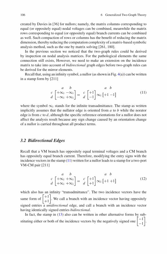
106 6 Generalized Two-Graph Theory
created by Davies in [36] for nullors; namely, the matrix columns corresponding toequal (or oppositely equal) nodal voltages can be combined, meanwhile the matrixrows corresponding to equal (or oppositely equal) branch currents can be combinedas well. Such compaction of rows or columns has the benefit of reducing the matrixdimension, thereby reducing the computation complexity of a matrix-based symbolicanalysis method, such as the one by matrix solving [261, 180].
In the previous section we noticed that the two-graph rules could be derivedby inspection on nodal analysis matrices. For the pathological elements the sameconnection still exists, However, we need to make an extension on the incidencematrix to take into account of bidirectional graph edges before two-graph rules canbe derived for the mirror elements.
Recall that, using an infinity symbol, a nullor (as shown in Fig. 4(a)) can be writtenin a stamp form by [211]
a bcd
[+≤i −≤i
−≤i +≤i
⎡
=a b
cd
[+1−1
⎡
≤i⎢+1 −1
⎣ (11)
where the symbol ≤i stands for the infinite transadmittance. The stamp as writtenimplicitly assumes that the nullator edge is oriented from a to b while the noratoredge is from c to d, although the specific reference orientations for a nullor does notaffect the analysis result because any sign change caused by an orientation changeof a nullor is carried throughout all product terms.
3.2 Bidirectional Edges
Recall that a VM branch has oppositely equal terminal voltages and a CM branchhas oppositely equal branch current. Therefore, modifying the entry signs with theincidence vectors in the stamp (11) written for a nullor leads to a stamp for a two-portVM-CM pair [211]
a bcd
[+≤i +≤i
+≤i +≤i
⎡
=a b
cd
[+1+1
⎡
≤i⎢+1 +1
⎣ (12)
which also has an infinity “transadmittance”. The two incidence vectors have the
same form of
[+1+1
⎡
. We call a branch with an incidence vector having oppositely
signed entries a unidirectional edge, and call a branch with an incidence vectorhaving identically signed entries bidirectional.
In fact, the stamp in (13) also can be written in other alternative forms by sub-
stituting either or both of the incidence vectors by the negatively signed one
[−1−1
⎡
.

3 Extension to Mirror Elements 107
Fig. 5 Reference orientationsfor the bidirectional VM andCM edges
d
a
b
VM CM
c
For example,a b
cd
[+≤i +≤i
+≤i +≤i
⎡
=a b
cd
[−1−1
⎡
≤i⎢−1 −1
⎣ (13)
is also a stamp for a VM-CM pair. In general, we have two oppositely signed incidence
vectors to represent a bidirectional branch,
[+1+1
⎡
or
[−1−1
⎡
. In symbolic analysis,
whichever choice would not affect the symbolic analysis results, because in generala sign change in the stamp changes all product term signs, resulting in a sum-of-product expression still equal to zero. As a convention, it suffices to use the positiveincidence vector for a bidirectional branch.
To differentiate from a unidirectional edge, we would place two opposite arrowson an edge to mark a bidirectional edge, see Fig. 5. Since a bidirectional edge wouldnot differentiate the two terminals (head and tail indistinguishable), we may place areference orientation beside the edge to differentiate the head from the tail in casea need arises. If an edge is known to be bidirectional, usually an arbitrary referenceorientation is placed.
Since there exists similarity between a nullor and a VM-CM pair, we may likewiseapply row-column merges (equivalent to edge collapse in two-graph) to the VM andCM elements. Intuitively, such operations can be applied to a bidirectional incidencevector as follows
ab
[+1+1
⎡
=∈ a{−a, b}
[+10
⎡
(14)
where the transformation is by multiplying the row-a by −1 and adding it to the row-b, resulting in the vector on the right side. The second row on the right is labeled bya set {−a, b}, indicating a nodal merge. Moreover, the minus signed a in the node setindicates the merge is a result of collapsing a bidirectional edge. Also, the notation{−a, b} implies that the row operation is from row a to row b, which follows thereference orientation given to the bidirectional edge, see Fig. 5.
Because the mirror edges (VM and CM) can be mutually paired with nullor edges(NL and NR), the following statement on the two-graph rule for the mirror elementswill include all the four possible cases of pairing. Note that Rule (iv) becomes aspecial case of the following rule.
(v) Two-graph rule for pathological elements: The NL or VM edge must beincluded in all trees spanning the V-graph and the NR or CM edge must be

108 6 Generalized Two-Graph Theory
CS
I−Graph
a
{a,−b}GVM
a
b V−Graph
VC
0
{−a,b}
b
I = (2G)VCS
VC
c
d
c
d V−Graph0
CS
I−Graph
GCM c,d
{c,−d}
I = (2G)VCS
(a)
(b)
Fig. 6 Parallel connections and equivalent conversions. a VM connected with G in parallel, b CMconnected with G in parallel
included in all trees spanning the I-graph. Each mutual pair of pathologicaledges (NL-NR, NL-CM, VM-NR, or VM-CM) must be included in all term-generating spanning tree-pairs and contributes a weight of unity.
3.3 Parallel Connection of G
The two-graph rule for nullor and mirror edges requires that such edges must beincluded in two-tree for term generation. However, it could happen that such patho-logical edges might be connected by an RCL (in general G) element in parallel. Thensuch G edges are automatically removed because loop is not allowed in a tree. Fornullor edges, such parallel connection of G element can be pre-excluded because bythe property of nullor any parallel connection of a G element is redundant.
However, a G element connected in parallel to a VM or CM branch is not redundantdue to the electrical property defined for the mirror element. Recall that a VM branchhas oppositely signed terminal voltages and a CM branch has oppositely signedterminal currents. When a G element is connected in parallel, shorting the VM orCM branch should maintain the electrical property of G. The following discussionshows that when a mirror edge is precollapsed, we may create an equivalent graphby modifying the G element.
When a VM-edge is collapsed in the V-graph, its two terminals a and b are mergedinto a node-set {a,−b} with nodal voltage V{a,−b} (referenced to the ground). Sincethe current in G satisfies IG = G(Va − Vb) = (2G)Va (because Va = −Vb), weget IG = (2G)V{a,−b}, where IG is oriented by the reference given to the VM. Anelement satisfying IG = (2G)V{a,−b} is a two-port VCCS (i.e., G-type) elementshown in Fig. 6a with the VC branch between the merged node {−a, b} and theground, and the CS branch between nodes a and b. The transadmittance of thiselement is (2G).

3 Extension to Mirror Elements 109
When G is connected in parallel to a CM branch, a similar argument goes asfollows. Let the two terminal voltages of the CM branch be Vc and Vd . Then, thecurrent flowing through G is equal to IG := G(Vc − Vd). Obviously, this current IG
is part of the current flowing away from node c, and also part of the current flowinginto node d. When the CM branch is collapsed by merging nodes c and d, with themerged node denoted by {c, −d}, the two partial currents IG become both flowing“away” from the merged node {c, −d} due to the minus sign attached to d. (Notethat this is the effect caused by collapsing a bidirectional edge.) The net current 2IG
should sink to the ground. Consequently, we end up with a current 2IG = (2G)Vc,d
flowing away from the merged node {c, −d} to the ground, as the result of collapsingthe CM branch connected by a G in parallel. The resulting equivalent graph edgesare illustrated in Fig. 6b. This argument is in fact equivalent to a row operation byadding the row d (multiplied by −1) to the row c, then eliminating the row d.
The above discussion results in the following rule for dealing with the case ofVM or CM connected by G in parallel.
(vi) Two-graph rule for (G ∧ V M) or (G ∧ C M): When a G-element is con-nected in parallel to a VM or CM (or a bidirectional edge in general), the VM orCM edge may be precollapsed in their existing graph (V-graph or I-graph) whilethe G-element should be converted to a VCCS of gain (2G) with the equivalentedges being placed as shown in Fig. 6.
4 Sign of Two-tree
In the two-graph method, a two-tree satisfying all edge pairing conditions is called anadmissible two-tree or tree-pair. An admissible two-tree generates a signed productterm, in which the term sign is determined by the incidence matrix of the two-tree[117].
For a network not containing mirror elements, the sign of a tree-pair is determinedas follows. For an example, suppose we have a graph of four nodes and four edges,e1, e2, e3, and e4. Let the incidence matrix be given on the left-hand side in (15)below, where by convention each edge is oriented from +1 to −1. Then a sequenceof row operations can extract a tree from the incidence matrix while determining thesign for the tree, which is described below.
e1 e2 e3 e4
1234
⎤
⎥⎥⎦
+1 0 −1 +1−1 +1 0 00 −1 0 −10 0 +1 0
⎛
=∈
e1 e2 e3 e4
1{1, 2}
34
⎤
⎥⎥⎦
+1 0 −1 +10 +1 -1 +10 −1 0 −10 0 +1 0
⎛
(15)
Select edge e1; add the row with +1 (tail of e1) to the other row with −1 (head ofe1); we get the matrix written on the right-hand side in (15), where the underscored
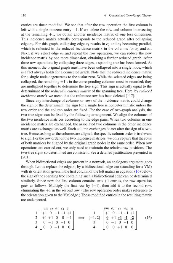
110 6 Generalized Two-Graph Theory
entries are those modified. We see that after the row operation the first column isleft with a single nonzero entry +1. If we delete the row and column intersectingat the remaining +1, we obtain another incidence matrix of one less dimension.This incidence matrix actually corresponds to the reduced graph after collapsingedge e1. For this graph, collapsing edge e1 results in e2 and e4 becoming parallel,which is reflected in the reduced incidence matrix in the columns for e2 and e4.Next, if we select edge e2 and repeat the row operation, we can reduce the newincidence matrix by one more dimension, obtaining a further reduced graph. Afterthree row operations by collapsing three edges, a spanning tree has been formed. Atthis moment the original graph must have been collapsed into a single node, whichis a fact always holds for a connected graph. Note that the reduced incidence matrixfor a single node degenerates to the scalar zero. While the selected edges are beingcollapsed, the remaining ±1’s in the corresponding columns must be recorded; theyare multiplied together to determine the tree sign. This sign is actually equal to thedeterminant of the reduced incidence matrix of the spanning tree. Here, by reducedincidence matrix we mean that the reference row has been deleted [117].
Since any interchange of columns or rows of the incidence matrix could changethe sign of the determinant, the sign for a single tree is nondeterministic unless therow order and the column order are fixed. For the case of two-graph analysis, thetwo-tree signs can be fixed by the following arrangement. We align the columns ofthe two incidence matrices according to the edge pairs. When two columns in oneincidence matrix are exchanged, the associated two columns in the other incidencematrix are exchanged as well. Such column exchanges do not alter the sign of a two-tree. Hence, as long as the columns are aligned, the specific column order is irrelevantto sign. For the row order of the two incidence matrices, we only require that the rowsof both matrices be aligned by the original graph nodes in the same order. When rowoperations are carried out, we only need to maintain the relative row positions. Thetwo-tree signs so determined are consistent. See a detailed justification presented in[201].
When bidirectional edges are present in a network, an analogous argument goesthrough. Let us replace the edge e1 by a bidirectional edge vm (standing for a VM)with its orientation given in the first column of the left matrix in equation (16) below,the sign of the spanning tree containing such a bidirectional edge can be determinedsimilarly. Since now the first column contains two +1 entries, the row operationgoes as follows: Multiply the first row by (−1), then add it to the second row,eliminating the +1 in the second row. (The row operation order makes reference tothe orientation given to the VM edge.) Those modified entries in the resulting matrixare underscored.
vm e2 e3 e4 g1234
⎤
⎥⎥⎦
+1 0 −1 +1 +1+1 +1 0 0 −10 −1 0 −1 00 0 +1 0 0
⎛
=∈
vm e2 e3 e4 g1
{−1, 2}34
⎤
⎥⎥⎦
+1 0 −1 +1 +10 +1 +1 -1 -20 −1 0 −1 00 0 +1 0 0
⎛
(16)
4 Sign of Two-tree 111
After the row operation with subtraction, some columns in the new incidencematrix have equally signed entries, implying that the collapse of one bidirectionaledge could likely make other unidirectional edges bidirectional. Such edge ori-entation changes are automatically managed by the incidence matrix, hence there isno extra cost for symbolic analysis, including the sign determination of two-trees.
For illustration, we also intentionally placed an extra edge g in the last column inequation (16) as a parallel edge to the VM . The row operation said above results inan entry of (−2) in the resulting incidence matrix. To maintain an incidence matrix,the factor 2 must be taken out and moved to the gain of the converted VCCS elementfor the parallel g. It provides another justification of the handling rule given in thepreceding subsection for a parallel connection of G with VM/CM.
5 Summary of Generalized Two-graph Rules
So far we have established the complete two-graph edge rules for enumerating alladmissible two-trees for any linear network containing all types dependence elementsand pathological elements. It is worthwhile to summarize all the edge pairing rulesaltogether in Fig. 7 to have an intuitive comparison.
As we mentioned before, the edge orientations will be reflected in the incidencematrix, which is then used to determine the sign of a two-tree. Hence, edge orienta-tions must be carefully managed throughout a symbolic analysis process. The edgeorientations are defined by the following convention.
Definition of Edge Orientations: The branch orientation of any current branch(no matter controlling, controlled, or independent) is defined by the given referencecurrent flow. For a controlling voltage port, the branch orientation is directed from thereference positive polarity to the negative polarity. For a controlled (or independent)voltage source, the branch orientation is defined to be from the negative polarity tothe positive polarity of the source. For memorization, the orientation of a voltageport is just the flowing current direction when we connect a resistive load to the port(which is a current-centric orientation strategy).
The edge orientations for the four types of dependent elements shown in Fig. 7are consistent with the definition above. The orientations of the nullor edges can bearbitrarily, hence the edges are undirected. The VM-CM edges are bidirectional andthe reference orientations given in Fig. 7(f) are just assigned arbitrarily.
Referring to the edge selection rules defined in Fig. 7, we can pre-allocate thegraph edges of dependent elements (including nullors and mirrors) in the V-graph andI-graph of two-graph as illustrated in Fig. 8. In general, the controlling and controllededges are separately allocated to the V-graph and the I-graph, respectively, exceptfor the CC and VS edges which may be selected as common (self-paired) edges intree-pairs. Hence, they are allocated to both graphs.
Besides the edge allocation rule illustrated by Fig. 8, we have other edge rulesspecific to the two-graph theory, which are named by the Edge Association Rule andthe Edge Priority Rule.

112 6 Generalized Two-Graph Theory
VS = E VC
VC VS
c
d
a
b
VC
a
b
a
b
VC
c
d
VS
V−Graph I−Graph
c
d
VS
CS = F CC
CSCC
b
a c
d
c
CS
d
a
b
V−Graph
CC
I−Graph
CC
c
d
CS
a
b
CS = G VC
a
db
c
VC CS
I−Graph
c
d
CS
a
b
VC
a
b
a
CS
b
VC
V−Graph
a
b
CC
c
d
VS
V−Graph
VS
c
d
I−Graph
a
b
CCVS
VS = H CC
a
b
c
d
CC
a
b d
c
Nullor
NL NR
a
b
c
d
NL
V−Graph
a
b
I−Graph
c
d
NR
a
b d
c
VM CM
VM−CM
c
d
V−Graph
VM
a
b
a
b
CM
c
d
I−Graph
(a)
(b)
(c)
(d)
(e)
(f)
Fig. 7 Two-graph edge selection rules for all dependent sources and pathological elements. aVCVS (E). b CCCS (F). c VCCS (G). d CCVS (H). d Nullor. e VM-CM. The darkened edges arethose must be selected
Edge Association Rule: Every admissible tree-pair consists of a set of pairededges, each pair is associated with a circuit element. Some edges are mutuallypaired while others are self-paired; but only one type of pairing is allowed foreach edge in an admissible tree-pair.
The edge priority is regarding to those graph edges that have higher priority informing spanning trees, which we mainly refer to those CC, VS, NL, NR, VM, andCM edges.

5 Summary of Generalized Two-graph Rules 113
CSVS CC
V−Graph
NLVM VC CCVS
I−Graph
NRCM
Fig. 8 Edge allocation in the initial two-graph. The CC and VS edges are allocated to both I- andV-graphs
Table 1 Edge pairing and symbolic weights
Type V-graph I-graph Weight Pairing Priority
VCVS VC VS E Mutual Exclusive(E) VS VS 1 Self compulsoryCCCS CC CS F Mutual Exclusive(F) CC CC 1 Self compulsoryVCCS (G) VC CS G Mutual OptionalCCVS CC VS H Mutual Exclusive(H) CC, VS CC, VS 1 Self compulsoryNullor NL NR 1 Mutual CompulsoryVM-CM VM CM 1 Mutual CompulsoryNL-CM NL CM 1 Mutual CompulsoryVM-NR VM NR 1 Mutual Compulsory
Edge Priority Rule: All term-generating admissible tree-pairs must includeall CC, NL, and VM edges in the trees spanning the V-graph, and must includeall VS, NR, and CM edges in the trees spanning the I-graph. In addition, the CCand VS edges can be either mutually-paired or self-paired in each admissibletwo-tree.
The above two rules are just general statements summarized for all dependentedges eligible for symbolic analysis. For clarity, it is helpful to make an element-wise summary on the edge selection rule, given in Table 1, which specifies both theedge pairing details and the associated symbolic weights. The edge selection priorityfor each element type is remarked in the last column. For those elements with twopairing possibilities, exclusive compulsory means one out of the two cases must beincluded in each two-tree. An optional pairing (only with a G-type element) meansthat such an edge pair may or may not be included in a two-tree. All cases of singularpairing (listed in the last four rows in the table) are compulsory, meaning that allsuch edge pairs must be included in all admissible two-trees.
An admissible tree-pair generates a symbolic product term by collecting the sym-bolic weights for all paired edges in the tree-pair. A unity weight is simply ignoredif it is multiplied by other symbols in a term. The term signs are determined by arowwise processing of the incidence matrices of a two-tree.

114 6 Generalized Two-Graph Theory
Fig. 9 Edge collapse nota-tions for the VM and CMbranches
V−graph
CM
I−graph
VM
a
b
c
d
VM
CM
{−a, b} {−c, d}
6 Compact Two-graph As Intermediate Form
The two-graph method for symbolic analysis is based on the enumeration of all admis-sible two-trees. The enumeration rules summarized in the previous section tell us thatthose nullor and mirror edges are the compulsory edges that must be included in alladmissible two-trees. Therefore, for implementation efficiency, all such compulsoryedges can be collapsed in the two-graph by preprocessing; the resulting two-graph iscalled a compact two-graph. The subsequent two-tree enumeration performed on thecompact two-graph would not alter the symbolic analysis result. In case a networkcontains quite a number of singular circuit elements, the preprocessing strategy canin general greatly improve the two-tree enumeration efficiency due to the reductionof the two-graph dimension. The main goal of this section is to demonstrate that acompact two-graph can be used as an intermediate network representation not onlyfor two-tree enumeration, but also for matrix-based nodal analysis.
The node set notation we introduced for labeling the rows during the row opera-tions of incidence matrices remain useful for representing nodes resulting from edgecollapses. For unidirectional edges, say, an NL or NR edge (a, b), the merged nodeis denoted by the node set {a, b}. For bidirectional edges, say, a VM or CM edge(a, b) of a reference orientation from a to b, the merged node is denoted by the setnotation {−a, b}, see the illustration in Fig. 5. Note that in case a is already a nodeset, −a is equal to the set containing all negated elements. Similar notations havebeen used by other authors, such as by Davies [36] for dealing with the nullors andby Sánchez-López et al. [180] for dealing with the pathological elements.
Precollapsing pathological (or singular) edges would in general make the nodenumbering of the V-graph and I-graph nonidentical. We have pointed out in Sect. 4that for sign determination the incidence matrix rows must be aligned according tothe node numbers, meanwhile the relative row order must be maintained wheneverany edge is collapsed. The maintenance of the relative row orders is necessary forthe sign consistence of two-trees.
The key difference between the two mainstream symbolic analysis methods, two-tree enumeration based and the nodal admittance matrix based, lies in how the
6 Compact Two-graph As Intermediate Form 115
independent sources are treated in the formulation. Without loss of generality weonly consider single-input single-output (SISO) linear networks; namely, a networkdriven by a single independent source and measured at a single output port. Thecases of multiple inputs and multiple outputs can be handled by the principle ofsuperposition.
6.1 Admissible Two-tree Enumeration
A single-input single-output transfer function can be treated as a dependent sourceelement with an unknown gain. Typically, it is more convenient to model the outputport as the controlling side and the input port as the controlled side. For example,suppose a network is driven by an independent voltage source Vin and an outputvoltage is measured at a port (a, b), denoted by Va,b. Let the input-output (I/O)transfer function be defined by Va,b = E · Vin , where E stands for the gain. Thiselement can alternatively be modeled by an inverted equation Vin = X · Va,b, whereX = 1/E becomes the gain and the port properties with this element satisfies therequirement for a VCVS element, i.e., the controlling port Va,b is an open voltageport while the controlled port Vin is a controlled source. This artificially definedVCVS element (called an I/O element) is treated equally as other linear elements inthe network. The symbolic terms generated by the two-graph rules can in generalbe divided into two parts, one part involving the symbol X as a factor while therest not. Since the network is treated as an undriven circuit, the sum of the signedproduct terms must be equal to zero [201]. Therefore, the unknown symbol X can besolved by a simple algebraic arrangement. For other types of I/O relations, a similartreatment applies. The examples presented in the next section will further illustratethe detailed procedure.
The two-tree based analysis requires that all edges in any two-tree be associatedin pairs, some mutually paired and the rest self-paired. Hence, before enumerationstarts, all edges in two-graph must have all edges in the V-graph paired with all edgesin I-graph. In contrast, if we use a two-graph representation for a nodal admittancematrix formulation, the edge-wise pairing requirement is not necessary, especiallyfor those compulsory CC and VS edges. This is because the electrical properties ofthe CC and VS edges allow us to contract them in the V-graph and I-graph withoutaffecting the formulation of the nodal admittance matrix.
6.2 Nodal Admittance Matrix Formulation
Recall that the notion of V-graph and I-graph in the classical two-graph methodwas derived from the nodal admittance formulation in matrix form for RCL-gm
networks. More specifically, the nodes in the V-graph define the nodal voltages whilethe branches in the I-graph define the KCL equations, i.e., the NAM rows. Now for
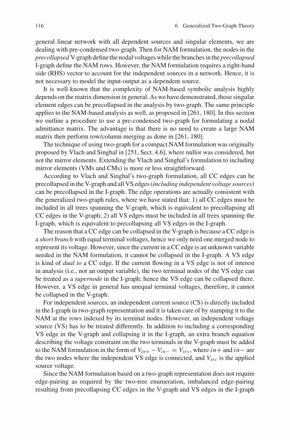
116 6 Generalized Two-Graph Theory
general linear network with all dependent sources and singular elements, we aredealing with pre-condensed two-graph. Then for NAM formulation, the nodes in theprecollapsed V-graph define the nodal voltages while the branches in the precollapsedI-graph define the NAM rows. However, the NAM formulation requires a right-handside (RHS) vector to account for the independent sources in a network. Hence, it isnot necessary to model the input-output as a dependent source.
It is well-known that the complexity of NAM-based symbolic analysis highlydepends on the matrix dimension in general. As we have demonstrated, those singularelement edges can be precollapsed in the analysis by two-graph. The same principleapplies to the NAM-based analysis as well, as proposed in [261, 180]. In this sectionwe outline a procedure to use a pre-condensed two-graph for formulating a nodaladmittance matrix. The advantage is that there is no need to create a large NAMmatrix then perform row/column merging as done in [261, 180].
The technique of using two-graph for a compact NAM formulation was originallyproposed by Vlach and Singhal in [251, Sect. 4.6], where nullor was considered, butnot the mirror elements. Extending the Vlach and Singhal’s formulation to includingmirror elements (VMs and CMs) is more or less straightforward.
According to Vlach and Singhal’s two-graph formulation, all CC edges can beprecollapsed in the V-graph and all VS edges (including independent voltage sources)can be precollapsed in the I-graph. The edge operations are actually consistent withthe generalized two-graph rules, where we have stated that: 1) all CC edges must beincluded in all trees spanning the V-graph, which is equivalent to precollapsing allCC edges in the V-graph; 2) all VS edges must be included in all trees spanning theI-graph, which is equivalent to precollapsing all VS edges in the I-graph.
The reason that a CC edge can be collapsed in the V-graph is because a CC edge isa short branch with equal terminal voltages, hence we only need one merged node torepresent its voltage. However, since the current in a CC edge is an unknown variableneeded in the NAM formulation, it cannot be collapsed in the I-graph. A VS edgeis kind of dual to a CC edge. If the current flowing in a VS edge is not of interestin analysis (i.e., not an output variable), the two terminal nodes of the VS edge canbe treated as a supernode in the I-graph; hence the VS edge can be collapsed there.However, a VS edge in general has unequal terminal voltages, therefore, it cannotbe collapsed in the V-graph.
For independent sources, an independent current source (CS) is directly includedin the I-graph in two-graph representation and it is taken care of by stamping it to theNAM at the rows indexed by its terminal nodes. However, an independent voltagesource (VS) has to be treated differently. In addition to including a correspondingVS edge in the V-graph and collapsing it in the I-graph, an extra branch equationdescribing the voltage constraint on the two terminals in the V-graph must be addedto the NAM formulation in the form of Vin+ − Vin− = Vsrc, where in+ and in− arethe two nodes where the independent VS edge is connected, and Vsrc is the appliedsource voltage.
Since the NAM formulation based on a two-graph representation does not requireedge-pairing as required by the two-tree enumeration, imbalanced edge-pairingresulting from precollapsing CC edges in the V-graph and VS edges in the I-graph

6 Compact Two-graph As Intermediate Form 117
VS = E VC
VC VS
c
d
a
b
a
b
c
d
VSVC
V−Graph
b{c,d}
VSVC
I−Graph
a
CS = F CC
CSCC
b
a c
d
a
b
CC
c
d
CS
I−Graph
{a,b}CS
d
c
V−Graph
CC
CC
{a,b}
V−Graph
c
d
VSVS
VS = H CC
a
b
c
d
CC
a
{c,d}
VS
I−Graph
CC
b
a
b d
c
Nullor
NL{c,d}
a
b
I−Graph
NRc
d
{a,b}
V−Graph
NLNR
dV−Graph
VM
{−a, b}
c a
b
I−Graph
CM
{−c, d}
a
b d
c
VM CM
VM−CM
(a)
(b)
(c)
(d)
(e)
Fig. 10 Precollapsed circuit elements for NAM formulation. a VCVS/E. b CCCS/F. c CCVS/H.d Nullor. e VM-CM
would not affect the NAM stamping. Obviously, the mentioned edge precollapsingcan further reduce the NAM dimension and thereby the complexity of symbolicanalysis by NAM.
Without using a condensed two-graph representation, the NAM formulationmethod proposed in the work [180] has to convert the CC and VS edges into VCCSelements by introducing unity resistors connected to the respective branches, which isequivalent to placing +1’s and −1’s in modified nodal analysis matrix. This methoddoes not help in further reducing the matrix dimension.
For an intuitive reference, those circuit elements that can be precollapsed are listedin Fig. 10, where the following rules are observed:
1. All CC branches are precollapsed in the V-graph.2. All VS branches are precollapsed in the I-graph.

118 6 Generalized Two-Graph Theory
3. By collapsing a unidirectional edge, the merged node is denoted by a union setof two unsigned node indexes or node sets.
4. By collapsing a bidirectional edge, the merged node is denoted by a union set oftwo oppositely signed node indexes or node sets.
Note that the minus-signed indexes maintained in the merged node sets will be takeninto account when the admittances of other regular circuit elements connected tosuch nodes are stamped into the nodal analysis matrix.
The procedure for building a nodal admittance matrix based on a compact two-graph representation is summarized in the following steps:
NAM Formulation by Compact Two-graph:
Step 1. Index the circuit nodes continuously by integers from 0 (for the ground)and up. Partition the circuit graph into a pair of V- and I-graphs with the V-graphcontaining all NL edges and VM edges, and the I-graph containing all NR edgesand CM edges (if such singular edges exist). Other edges are allocated accordingto the two-graph rules.
Step 2. Collapse all singular edges on their respective graphs. Whenever an edgeis collapsed, the two terminal nodes are merged and indexed by a node-set. ForVMs and CMs, the node indexes in the node-sets are oppositely signed accordingto the reference orientations.
Step 3. Collapse all CC edges in the V-graph and all VS (including independentVS) edges in the I-graph.
Step 4. The voltages at the nodes or node-sets in the reduced V-graph are desig-nated the unknown voltage variables (corresponding to the columns of the NAM),while the nodes or node-sets in the reduced I-graph are where the KCL equationsare written (corresponding to the rows of the NAM).
Step 5. When stamping an admittances to the NAM rows, if it is connected to aminus-signed node, the regular sign of the admittances must be flipped.
Step 6. A branch equation for an independent voltage source (VS) is added to theNAM according to its connection in the V-graph.
The advantages of using a compact two-graph representation for NAM analysisof networks containing singular elements are summarized here:
1. It avoids building a large NAM followed by reduction. The associated operationsusually require scanning the rows and columns of NAM for several times. Bythe condensed two-graph formulation, computer implementation becomes muchsimpler.
2. The condensed two-graph formulation allows further collapsing the VS edges inthe I-graph and the CC edges in the V-graph, resulting in a further reduced NAMfor symbolic analysis.

7 Examples 119
G+
x
yz−
z+x
y
Vin
1
2
1
ICCII−
ICCII+2Y Y
G
Fig. 11 ICCII-based voltage-mode filter
ICCII+
+
34
2 51
VM1
Vin
VM2
NR1
CM2
1
2
1
G
G
2Y Y
ICCII−
Fig. 12 Circuit model after substituting pathological elements
7 Examples
We use two examples in this section to illustrate the two symbolic analysis proceduresbased on the compact two-graph representation method. All the necessary steps aregiven in detail. It is expected that the detailed steps are helpful for a computerimplementation of the proposed procedures.
Example 1 is a filter shown in Fig. 11, which is composed of two ICCII (sec-ond generation current conveyor) blocks, one positive-type (ICCII+) and the othernegative-type (ICCII-). This circuit was studied in [210] and later used as an examplefor NAM symbolic analysis in [261,180]. In terms of mirror and nullor elements,an ICCII+ element is just a pair of VM-CM and an ICCII- element is just a pair ofVM-NR. For symbolic analysis, we substitute the current conveyor blocks by theirprimitive pathological elements, resulting in the equivalent network shown in Fig.12, where arbitrary reference orientations have been assigned to the VM and CMedges.

120 6 Generalized Two-Graph Theory
Fig. 13 Compact two-graphfor NAM analysis
I−graph
1
Vin
G 2
Y2
Y1
1
{−2,3}
5
{0,−4}
G 1
G 2
Y1
Y2
{0,1}
{−3,4}
{2,5}
V−graph
G
Since this circuit involves two pairs of singular edges, these edges can beprecollapsed to create a compact two-graph. Depending on whether a NAM formu-lation or tree-pair enumeration is used, two slightly different compact graph-pairsare created.
Shown in Fig. 13 is a pair of reduced V-graph and I-graph for NAM analysis, wherethe edge pairs VM-CM and VM-NR are precollapsed. The node sets introduced inthe reduced graphs reflect the result of edge collapses. Also, note that the independentvoltage source Vin is included in the V-graph, but collapsed in the I-graph, resultingin a merged node {0, 1} in the I-graph.
The compact two-graph obtained above can be used for stamping a NAM accord-ing to the NAM Formulation Steps described in Sect. 6.2:
V1 V{−2,3} V5 RH Sbr_Vin
{2, 5}{−3, 4}
⎤
⎦1 0 0
−G1 −G1 G2 + Y20 −Y1 −G2
⎛
⎤
⎦Vin
00
⎛ (17)
The first row in (17) is a branch equation describing the independent voltagesource Vin . The second row stands for the KCL equation at the merged node {2, 5}of the I-graph, where the elements G1, G2, and Y2 are connected. These elementsinvolve the nodal voltages V1, V2 and V5 in the V-graph. Since the notation V{−2,3}is used for the node-set after merging nodes 2 and 3 in the V-graph (where the edgeV M1 is connected), the admittance G1 connected to node 2 must be sign-flipped,giving −G1 in the entry (2, 2) of the matrix. The entry (−Y1) in the entry (3, 2) hasbeen sign-flipped as well due to the row index {−3, 4} and the connection of theelement Y1 between (3, 0) in the original circuit. Solving the matrix equation givesthe same results as derived in [180, Eqns (54-55)] and [261, Eqns (12-13)].
The second symbolic analysis method is by tree-pair enumeration, for which thecompact two-graph is created in Fig. 14. By choosing the nodal voltage at node 5 forthe output, the input-output relation is modeled by a VCVS element written in theform of Vin = X Vout , where X is the gain symbol.
Shown in Fig. 15 are the four admissible tree-pairs enumerated from the createdcompact two-graph. These two-trees generate the following four signed terms that

7 Examples 121
{−3,4}1
Vin Y1
G 2 Vout
Y2
1
{−2,3}
5
{0,−4}
(VS)(VC)
G 2
Y1
Y2
G 1
Vin
V−graph I−graph
{2,5}
(VS)
1
0
G
Fig. 14 Compact two-graph for tree-pair enumeration
Tree−pair 3
X
G 1
G 2
{0,−4}
1
{−2,3}
5 G 1
VSX
G 2
0
{2,5}1
{−3,4}
Y1
Y2
{0,−4}
5
{−2,3}
1
Y1
Y2
Tree−pair 10
{−3,4}
1 {2,5}
VSX G2
Y1 VS
X Y1
G2
Tree−pair 2{0,−4}
1
{−2,3}
5
0
{2,5}1
{−3,4}
Y1
G 1
VCX
{0,−4}
1
{−2,3}
5
Y1
G 1
VSX
0
{2,5}1
{−3,4}
Tree−pair 4
VS
Fig. 15 Four admissible tree-pairs for the two-graph in Fig. 14
are summed to zero:
Y1Y2 + Y1G2 + G1G2 − XG1Y1 = 0. (18)
We see that among the four terms one term is multiplied by X . Simply separatingthe terms, we can solve (1/X) to obtain the following transfer function
H(s) = Vout
Vin= 1
X= G1Y1
Y1Y2 + Y1G2 + G1G2, (19)
which is identical to the result obtained by the NAM formulation. Note that, fordetermining the term signs in (18), we have to assign arbitrary orientations to thoseundirected edges for the passive elements. The initially assigned orientations mustbe maintained in all admissible tree-pairs so that the generated signs are consistent.

122 6 Generalized Two-Graph Theory
CXCCII
n
Z p
Zn
X p
Y
X n
Z p
Zn
X p
Y
M2RM1R
M3R
C1
inI o,LP
I
o,BPI
1
2
3
4
5C
2
6
7
CXCCII
X
Fig. 16 DXCCII-based current-mode filter
DXCCII
X n
Z p
Z n
X p Xp
X n
Zp
Z n
NL 1
VM2
CM1
CM2
VY
IXp
IXn
IZp
I Zn
Y
Y
Fig. 17 Pathological circuit model for a DXCCII block
V−graph
in C1
M22G
M32G
M12G
2C
I−graph
{−1,6} {2,−4}
{3,5,−0}
M22G
2CM12GC 1
M32G
0
{4,5,−6}{1,2,−3}
I
Fig. 18 Compact two-graph representation of the DXCCII filter for NAM analysis
Example 2 considers the Dual X Current Conveyor (DXCCII) filter shown inFig. 16 ([276]), which was also an example in [261]. This circuit consists of twoDXCCII blocks, each can modeled by the pathological elements as shown in Fig. 17,which includes a NL-CM pair (a.k.a. CCII+) and a VM-CM pair (a.k.a. ICCII+).
By choosing arbitrary reference orientations for the pathological elements, weprecollapse these edges to create two compact two-graphs. The two-graph created inFig. 18 is used for NAM analysis while the one created in Fig. 19 is used for tree-pairenumeration.
In the former case the input current is the only independent source, which isincluded in the I-graph. In the latter case we choose Io,L P at node 7 (see Fig. 16) as

7 Examples 123
{2,−4}2G
M12GC 1M3
2G2C
I out
0
{4,5,−6}{1,2,−3}
V−graph
(CC)
7
Iin C 1
M12G 2C
M32G
M22GIout
I−graph
{−1,6}
(CC)(CS)
{5,7}
{3,−0}
M2
Fig. 19 Compact two-graph representation of the DXCCII filter for tree-pair enumeration
the output current Iout ; the I/O forms a CCCS element in the two-graph. Note that aftercollapsing the pathological edges, we find that the three resistors RM1, RM2, and RM3become loops connected to the merged nodes whose index sets contain negatively-signed indexes. According to the Parallel-G Connection Rule we described earlierin Sect. 6, these G-elements have to be converted to VCCS elements with gains2G M1, 2G M2, and 2G M3 as shown in the Figs. 18 and 19. We find that the reducedtwo-graphs are greatly more compact than the original network.
The NAM formulation leads to the following 2 × 2 matrix system:
V1,2,−3 V{4,5,−6} RH S{−1, 6}{2,−4}
[−2G M,2 − C1s −2G M32G M1 −C2s
⎡ [−Iin
0
⎡(20)
The output current Io,L P is solved indirectly by solving V4 first, then using theformula Io,L P = 2G M3V4 to get
Io,L P = Iin4G M1G M3
(2G M2 + C1s)C2s + 4G M1G M3(21)
Alternatively, we can use the two-graph shown in Fig. 19 to derive the samesymbolic result by tree-pair enumeration. Three admissible tree-pairs are shown inFig. 20. Actually, there is supposed to be four tree-pairs, but we have drawn the thirdtree-pair by including a pair of parallel edges C1 ∧ 2G M2. These tree-pairs generatethe following three signed terms summed to zero:
− X (2G M1)(2G M3) + (2G M1)(2G M3) + C2s (C1s + 2G M2) = 0. (22)
The transfer function is obtained by solving (1/X),
H(s) = Io,L P
Iin= 1
X= (2G M1)(2G M3)
(2G M1)(2G M3) + C2s (C1s + 2G M2)(23)
which is identical to that solved in (21).

124 6 Generalized Two-Graph Theory
Tree−pair 2
2G
M32G
{−1,6}
{3,−0}
(CS)
{2,−4} {5,7}
C 1
M22G 2C
0
{4,5,−6}{1,2,−3} 7
(CC) M22G 2C
C 1
{3,−0}
{−1,6}{2,−4} {5,7}
(CC)
M12GM3
2G
0
{1,2,−3} {4,5,−6}
7
(CC)M12G
M32G
0
{1,2,−3} {4,5,−6}
7
(CC)M12G
M32G
{5,7}
{3,−0}
(CC)
{2,−4}{−1,6}
Tree−pair 1
Tree−pair 3
M1
Fig. 20 Three admissible tree-pairs for the two-graph in Fig. 19. In the third tree-pair parallel edgesC1 ∧ 2G M2 are included
8 Summary
Both of the two-graph method and the nodal admittance matrix method are well-known in the literature on symbolic network analysis. However, their interrelationhas not been fully studied in an explicit way as presented in this chapter, especiallyin their connection to singular network elements. For historical reasons, until veryrecently many researchers (see for example [45, Chapter 6]) have not recognizedthat the classical two-graph method limited to RCL-gm networks has already beengeneralized by many authors in a variety of ways. However, it is obvious that theextended results lack unification.
A comprehensive overview on the generalized two-graph theory has been pre-sented in this chapter. The presentation is made as intuitive as possible by makingconnection to the inherently related nodal admittance matrix formulation. The gen-eralized two-graph theory has been developed in a unified form to include all linearnetwork elements, covering all types of dependent source, the nullor element, andthe most recently introduced pathological mirror elements. It has been demonstratedthat the generalized two-graph theory can deal with the mirror elements by introduc-ing bidirectional edges in the two-graph representation. It is further emphasized thatprecollapsing singular edges not only compresses the size of graph representation,but also provides convenience in applying a NAM-based symbolic analysis.
This chapter is solely dedicated to the theoretical aspects of the two-graph method.The computer implementation issues based on the generalized two-graph theory willbe discussed in the next chapter

Chapter 7Graph-Pair Decision Diagram
1 Introduction
In Chap. 3 we introduced a technique to formulate the spanning-tree enumerationproblem into a BDD construction problem. The BDD-based tree enumeration doesnot go through all spanning trees explicitly because the sharable subtrees are notenumerated twice. Therefore, the BDD-based tree-enumeration is truly an implicitenumeration strategy. In contrast, by explicit enumeration we mean that all the nec-essary symbolic product terms are enumerated one after another exhaustively. Thebenefit of implicit enumeration has already been demonstrated by an implementationof the DDD algorithm in Chap. 4. The main task of this chapter is to present anotherBDD-based implementation strategy for enumerating all admissible two-trees forany given linear network. This chapter is a continuation of the previous chapter byemphasizing the computer implementation issues of the enumeration rules developedthere.
In the previous chapter we have shown that a linear circuit also can be solved bya topological method (i.e., by processing the circuit graphs), which does not requirematrix formulation and solving. By directly enumerating a set of admissible two-trees, a corresponding set of symbolic product terms can be generated, from whicha symbolic transfer function can be derived. However, the main difficulty of directlyapplying this method to symbolic circuit analysis is its complexity. Typically, thetotal number of terms for analyzing an average size operational amplifier circuitcould be in the scale of 1015–1020, which is intolerable for most modern desktopcomputers in time and memory.
Fortunately the BDD technology can help to reduce the enumeration complex-ity greatly. A main development to be made in this chapter is to reformulate thetree-enumeration rules into another form of graph reduction rules. As an origi-nal pair of graphs are reduced by following an order of the circuit elements, theintermediately generated subgraph-pairs can find sharing among themselves. Such
G. Shi et al., Advanced Symbolic Analysis for VLSI Systems, 125DOI: 10.1007/978-1-4939-1103-5_7,© Springer Science+Business Media New York 2014

126 7 Graph-Pair Decision Diagram
subgraph-sharing can be efficiently managed by a BDD, which leads to a datastructure called Graph-Pair Decision Diagram (GPDD). As a matter of fact, theGPDD construction method involves a set of algorithms, which will be introducedin this chapter.
The rest of the chapter is organized as follows. Section 2 formulates the symboliccircuit analysis problem in the form of tree-pair enumeration. Section 3 reformulatesthe tree-pair enumeration algorithm into an implicit graph-pair reduction procedureby which a GPDD is constructed. The implementation details of GPDD are describedin Sect. 4. An efficiency comparison of GPDD to DDD is reported in Sect. 5. In Sect. 6we make a discussion on the term cancellation problem with symbolic analysis andemphasize that GPDD is a cancellation-free method. Section 7 concludes the chapter.The main content of this chapter is based on the contribution published in [201].
2 Definitions and Main Result
The GPDD method developed in this chapter is targeted for analyzing small-signalanalog integrated circuits. We temporarily exclude the pathological mirror elementsfor a self-contained presentation. Including the mirror elements is more or lessstraightforward by incorporating the edge rules developed in Chap. 6. We shall con-tinue using the abbreviations for the dependent sources introduced earlier, namely,the E , F , G, and H type elements for the dependent sources of VCVS, CCCS, VCCS,and CCVS, respectively. Nullor is also included.
The basic circuit elements eligible for GPDD analysis satisfy the followingassumption.
Assumption 7.1 The eligible circuit elements for GPDD analysis are:
• all linear lumped elements including impedance (Z), admittance (Y), dependentsources (VCVS, CCCS, VCCS, and CCVS), nullor, and independent current andvoltage sources.
The GPDD construction is completely based on the generalized two-graph theory.Before the construction starts, an initial two-graph must be created according to thefollowing rules. Without loss of generality we assume throughout this chapter that alinear network for GPDD analysis is SISO (single-input single-output).
Definition 7.1 (Rules for Initial Graph Construction) The initial graph for GPDDanalysis is created according to the following rules:
1 All the dependent source edges are oriented as follows: a VS edge is oriented fromthe polarity − to + (in the direction of a current flowing out of the positiveterminal), and a CS edge is just oriented by the assigned reference.
2 A VC edge is placed in the graph corresponding to the port where the controllingvoltage is. In case one voltage controls m (m > 1) sources, place m parallel edgesto the controlling voltage port, each edge is coupled to one controlled source.

2 Definitions and Main Result 127
3 A CC edge is placed in the graph for a controlling current branch. In case onecurrent branch controls m sources (m > 1), place cascaded m edges in series tothe graph, each is coupled to one controlled source.
4 Any relayed dependent sources are broken up to pairwise coupled edges. Forexample, if edge a controls edge b, and edge b controls edge c. Then place anextra edge b≤ in parallel to b if b is a voltage (or in series to b if b is a current) sothat edge b≤ is coupled to edge c.
5 An ideal opamp is replaced by a pair of nullor edges, i.e., a pair of NL (nullator)edge and a NR (norator) edge; their orientations can be assigned arbitrarily.
6 The selected input and output are modeled by a dependent source, with the outputport controlling the input port. The edges are oriented according to the specificationdefined in item 1.
In small-signal analysis of analog circuits, the symbols forming a product terminclude passive elements R, C, L and dependent sources E, F, G, H. The passiveelements are associated with common edges in the two-graph representation whilethose dependent elements are associated with mutually paired edges. In the s-domain(i.e., the frequency-domain), the symbolic entity for a capacitor C is Cs which is inadmittance form (denoted by a generic symbol Y ) and the symbolic entities for Rand L are respectively R and Ls, which are in impedance form (denoted by a genericsymbol Z ). In GPDD all impedance elements are manipulated in admittance forms.Thus a Z-element will be manipulated in the admittance form of Z−1. For brevitywe shall only make rule statements for the Y-elements.
For convenience we shall refer to the two trees in an admissible tree-pairs byan I-tree and V-tree, which span the I-graph and the V-graph, respectively. In casethe two trees in a tree-pair have all edges common, the tree-pair degenerates to asingle common tree. Recall that in the two-graph theory, a controlling edge is alwaysplaced in an V-tree and a controlled edge is placed in an I-tree if such edges appearas mutually paired edges.
Symbolic analysis by the two-graph theory generates symbolic product termsby collecting the circuit element symbols appearing on an admissible two-tree. InChap. 6 we have already stated the generalized two-graph rules. The statement madebelow for an admissible two-tree is more oriented toward computer implementation.The reader should pay special attention to the CC and V S edges which play tworoles in edge pairing.
Definition 7.2 (Admissible Two-tree Rules) The edges forming an admissible tree-pair must satisfy the following conditions:
1 The two edges of a nullor (if exist) must be included as paired-edges in alladmissible tree-pair.
2 All CC and VS edges (if exist) must be included in all admissible tree-pairs, butcan act either as common or as paired edges.
128 7 Graph-Pair Decision Diagram
3 The edges of a VCCS (G) are optional for inclusion in an admissible tree-pair.Whenever included, they must appear as paired edges.
4 The Y edges (including Z edges) are optional for inclusion in an admissibletree-pair. Whenever included, such an edge can only act as a common edge.
Remark 3 Recall that all CC and NL edges must be included in all admissibleV-trees, and all VS and NR edges must be included in all admissible I-trees. Thisimplies that these edges cannot form loops in their respective graphs. Otherwise, thecircuit must be unsolvable.
A signed symbolic product term is generated by an admissible tree-pair accordingto the rules stated next.
Definition 7.3 (Rules for Term Generation) A signed symbolic product term is asigned product of the symbols extracted from the edges included in an admissibletree-pair.
1 Common edge: A common admittance edge Yi contributes a symbol Yi , and acommon impedance edge Zi contributes a symbol Z−1
i . A common CC or VSedge contributes a factor unity.
2 Paired-edge: Two paired edges contribute a symbol by its gain; namely, eachtype of dependent sources contributes a symbol of Ei, j , Fi, j , Gi, j , or Hi, j . Inparticular, a nullor contributes a unity factor.
3 Term sign: The term sign of an admissible tree-pair is defined to be the determi-nant product of the two reduced incidence matrices, the details of which will beexplained later. As a special case, when an admissible tree-pair is a common tree,the term sign must be positive.
The two-graph method treats a pair of single-input and single-output as a depen-dent source as described earlier. With this assumption, the product terms generatedby all admissible tree-pairs must sum to zero, which is stated as a theorem.
Theorem 7.1 (Fundamental Two-graph Theorem) Given any linear circuit contain-ing elements satisfying Assumption 7.1, the signed product terms generated by alladmissible tree-pairs as defined by Definition 7.3 are cancellation-free, and the sumof them is equal to zero.
Proof A complete mathematical proof can be found in [201]. An intuitive circuitinterpretation of this theorem has been presented in Chap. 6. �
3 Implicit Enumeration by BDD
Theorem 7.1 provides a theoretical ground for the two-graph method for symboliccircuit analysis. However, directly enumerating all admissible tree-pairs is not rec-ommended for application, as we have already mentioned. To make the general-ized two-graph method practical, the currently known best strategy is to adopt a

3 Implicit Enumeration by BDD 129
BDD-based construction and make the tree-pair enumeration implicit. The ideaintroduced for the Modified Minty Algorithm for spanning tree enumeration in Chap. 3can now be applied. By this algorithm tree enumeration is reformulated into a graphreduction procedure.
The essence of the Minty’s algorithm [136] is to enumerate all spanning trees of aconnected graph by an exhaustive process of binary decompositions, in each step onegraph edge is selected for inclusion or exclusion. After reformulation, the ModifiedMinty Algorithm (refer to Chap. 3) replaces one of the binary edge operations, i.e.,“including an edge”, by “collapsing an edge”. A finite number of successive collapseand removal of the graph edges can either reduce a connected graph into a singlenode or make it disconnected. In the former case, i.e., a graph is reduced into a node,the collapsed edges in the course of binary decomposition must form a spanning tree.
A direct advantage of the Modified Minty Algorithm is that the intermediatelyreduced graphs can be compared for sharing, which is a property not available tothe original Minty’s algorithm. Analogously, by applying this modification to two-graphs, we have the property of two-graph sharing as well. The most efficient methodto manage sharing is by incorporating BDD, in which the two-graph shareables areidentified by hashing.
With two-graph, edge collapses and removals are performed on the basis of edge-pairs, common or different. In symbolic analysis, the circuit elements are identifiedby a set of symbols. For BDD construction, this set of symbols will be ordered andthe edge processing follows such a preselected order.
The two-graph reduction starts from a pair of initial graphs, which consists ofa current-graph (i.e., I-graph) and a voltage-graph (i.e., V-graph). The admissibleedge rules defined by Definition 7.2 leads to the following edge allocation rules forthe initial pair of graphs.
Definition 7.4 (Initial Graph-Pair) Let G be the initial circuit graph created accord-ing to Definition 7.1.
1 The initial I-graph consists of all edges from graph G but all VC edges and allNL edges.
2 The initial R-graph contains all edges from graph G but all CS edges and all NRedges.
Since all nullor edges must be present in all admissible tree-pairs (see Defini-tion 7.2), they can be collapsed in advance before the graph-pair reduction processstarts. Noticing that each nullor contributes a symbol of unity to all product terms byDefinition 7.3, the precollapse of a nullor has no effect on the term generation at all.
Preprocessing Nullor Edges: Collapse all NR edges in the I-graph and all NLedges in the V-graph pairwise. Renumber the merged nodes properly after collapsingan edge.

130 7 Graph-Pair Decision Diagram
Table 1 Edge operations forgraph-pair reduction
INCLUDE EXCLUDE
I-graph V-graph I-graph V-graphY Short Y Short Y Open Y Open YE (VCVS) Short VS Short VC Short VS Short VS
Open VS Open VCF (CCCS) Short CS Short CC Short CC Short CC
Open CC Open CSG (VCCS) Short CS Short VC Open CS Open VCH (CCVS) Short VS Short CC Short CC Short CC
Open CC Open VS Short VS Short VS
3.1 Edge-Pair Operations
By the definition of initial graph-pairs, translating the admissible edge pairing rulesto a set of pair-wise edge reduction rules is straightforward. Assuming that all nulloredges have been preprocessed, the edge-pair operations for the rest types of symbol,namely, Y , E , F , G, and H , are summarized in Table 1. The two columns named byINCLUDE and EXCLUDE represent the two decisions made at each step of the BDDconstruction. In the table, “Short” stands for collapse (or contraction) and “Open”for removal (or delete) of an edge.
For BDD construction, the binary decisions are defined in terms of whether aspecific symbol is included in a product term or not. In all cases, including a symbolmeans a pair of edges, common for Y and mutually paired for E , F , G, and H , arecollapsed. However, for excluding a symbol, only the Y and G types of edges areremoved whereas the common CC and VS edges must be collapsed for the E , F ,and H types of elements.
Note that for those elements involving compulsory CC and VS edges, these edgesact in two roles, but exclusively. Hence, whenever they act in one role, the unusededge must be removed. For example, when applying INCLUDE on a VCVS (E)element, the edge operations on the V-graph are “Short VC and Open VS”, whereOpen VS is because the VS edge on the V-graph is unused.
3.2 Construction of GPDD
Application of BDD to a specific problem requires at least three main components:the first is a definition of the binary decisions, the second is the design of a hash tableincluding the selection of hash objects, and the third is the selection of a symbol order.We have already defined the binary decisions for GPDD in terms of graph edgeoperations. When we were developing the graph-pair reduction rules, we alreadyhinted that the reduced graph-pairs were going to be the objects for hashing orsharing.

3 Implicit Enumeration by BDD 131
VcC
1 2
0
R
Vs
1
0
R
VsC
Vc
2
(b)(a)
Fig. 1 a RC circuit. b Graph
Sharing a pair of graphs is based on identifying that both reduced I-graphs andboth reduced V-graphs are respectively identical by comparing their respective edgesand nodes. To facilitate graph comparison, all graph edges should have been assignednames which are carried with the edges throughout the whole reduction process. How-ever, the graph nodes (commonly indexed by numbers) are not maintained throughoutthe reduction. Whenever two nodes are merged by collapsing an edge, the mergednode has to be assigned a new number. A proper node renumbering strategy couldaffect the efficiency in graph hashing. We shall further discuss on this issue later.
As a standard BDD construction process, all symbols appearing in the constructionshould be given an order first. Symbol order is also a factor that greatly affects theconstruction efficiency and the runtime efficiency. We defer the detailed selectionof a symbol order to the section on experiment. Given a symbol order, the graph-pair reduction process basically consists of many sequences of edge collapses andremovals according to the rules defined in Table 1.
Let us go through the GPDD construction process for a simple circuit first tointroduce some necessary terminologies for describing a GPDD data structure. Wewould like to derive the transfer function of the RC circuit shown in Fig. 1a from theinput voltage Vs to the output voltage Vc across the capacitor. For GPDD construction,an initial graph is created in Fig. 1b according to the Definition 7.1. In the initialgraph an extra Vc edge has been introduced for the output voltage. As we said before,the two-graph method is based on representing the input-output (I/O) relation by adependent source. In this example the I/O is naturally modeled by a VCVS defined byVs = X ·Vc, where X is the unknown gain symbol. (Refer to the item (6) of Definition7.1.) By inspection the transfer function of this example is H(s) = 1/(1 + RCs).
Three symbols R, C , and X are involved in this example. Define an order X <
R < C (where “<” reads “precedes”). The graph-pair reduction process is illustratedin Fig. 2. The root vertex is named by the unknown symbol X , to which an initial pairof graphs are attached. The edges allocated to the initial graphs follow the Definition7.4. Note that the VS edge is allocated to both I-graph and V-graph because thisedge could be common. The passive R and C edges are always assigned to the bothgraphs. The VC edge is allocated only to the V-graph.
Two arrows emanate from the root vertex, the solid arrow stands for the INCLUDEdecision and the dashed arrow for the EXCLUDE decision. Since X is a VCVS

132 7 Graph-Pair Decision Diagram
+R R
C
X
2
0
CR
2
0
CR
2
0
C
2
0
C
0
1
0
2
CVS
R1 2
0
R
VCVS
C
1
1
0
R
2
0
CR
+Open R
+
Open C+
+
Short VS
Short R
Short VS
Open VCShort VC
Open VS
+Short VS
Short R
Short C
+
Open R
Fig. 2 Illustration of GPDD construction
(E-type) symbol, the INCLUDE decision applies a paired edge collapse of VS-VCto the initial graph pair, leading to the reduced graph-pair attached at the vertex“R” pointed by the solid arrow. Note that edges forming loops after collapse areremoved for conciseness. On the other hand, the EXCLUDE decision at the symbol“X” applies the collapse of the VS-edge as a common edge to the initial graph pair,leading to another pair of reduced graphs attached at the vertex “R” pointed by thedashed arrow. When reducing the common VS-VS pair in this case, the VC-edge inthe V-graph does not play a role and is removed.
Both decisions involve edge-pair collapses, resulting in merged nodes. In thisexample, we always keep the smaller node number when collapsing an edge.
The two graph-pairs attached to the two “R” vertexes can be reduced further. Nowwe have finished the edge operations for the first symbol “X” and come to the edgeoperations on the second symbol “R”. R is a common edge element whose operationsgo as follows: the INCLUDE decision collapses this edge in both graphs attachedat the current R-vertex while the EXCLUDE decision simply removes this edge inboth graphs .
Looking at the graph-pair attached at the left “R” vertex in Fig. 2, the INCLUDEdecision reduces both graphs into a single node, implying that a spanning tree-pair hasbeen collapsed and the reduction should be terminated. The edges collapsed all theway, denoted by the path “X-R”, are the edges of the spanning tree-pair. In GPDD, weterminate this path at the special GPDD vertex “1”. On the other hand, the EXCLUDEdecision applied to the left “R” vertex results in a disconnected right-graph (i.e.,V-graph) (while the left-graph or I-graph contains a single C edge), which implies thatthe generated graph-pair is not valid for further reduction anymore. In other words, noadmissible spanning trees will be generated by following this reduction path further.

3 Implicit Enumeration by BDD 133
Fig. 3 A triple of GPDDvertices
f
Kσ σK
K’K K’f
Such a decision arrow should be terminated at the special GPDD vertex “0”. Thereduction paths subordinate to the right “R” vertex can be explained analogously. InFig. 2 the decision arrows are annotated by the associated edge operations for betterunderstanding.
We note that signs are attached to the decision arrows in the constructed GPDD inFig. 2. They are determined by a sign determination algorithm, which is a recursivealgorithm derived from the incidence matrices. The details on sign determinationrequire some technical development and are defer to a later section.
The signs and the symbols passed by along a path from the root down to the vertex“1” (called a 1-path) are multiplied together to generate a signed product term. Notethe following simple fact: the solid and dashed arrows created in GPDD constructionwould respectively stand for multiplications and additions when the created GPDDis used for numerical calculation. Because GPDD is a recursive data structure forcomputation in symbolic analysis, the signs attached to the decision arrows also aredetermined recursively. Hence, in the GPDD-based symbolic analysis, a term signis not calculated after a whole spanning tree-pair is generated, as we discussed inChap. 6. The recursive sign calculation method is in general more efficient.
We denote by Path(a-b-c≤-d) a path including vertexes a, b, and d, but excludingvertex c, which is denoted by the primed notation c≤. A primed symbol is at a vertexfollowed by a dashed arrow along the path. The GPDD shown in Fig. 2 containsthree 1-paths. 1) Path(X-R-1) generates the signed term (−X R−1) (note that theimpedance symbol is inverted); 2) Path(X ≤-R-1) generates the signed term (+R−1);3) Path(X ≤-R≤-C-1) generates the signed term (+Cs). By Theorem 7.1, the sum ofthese three terms is equal to zero. Hence, we get −X R−1 + R−1 + Cs = 0, fromwhich the symbolic transfer function is solved as H(s) = 1/X = 1/(1 + RCs).
3.3 Symbolic Expressions in GPDD
Since the symbolic computation performed by a GPDD is based on bottom-up recur-sion, every GPDD vertex produces a subexpression, with the two terminal vertexesgiving the two trivial expressions 1 and 0.
The generic computation performed at each GPDD vertex can be represented bythree neighboring vertexes connected as shown in Fig. 3, with the top vertex named bythe symbol K and the two descendant vertices representing the two subexpressionsfK and fK ≤ computed respectively by the solid-arrow-descendent vertex and thedashed-arrow-descendent vertex. The signs attached to the two decision arrows aredenoted by σK and σK ≤ . Then the expression computed by the top vertex K in Fig. 3

134 7 Graph-Pair Decision Diagram
is given byσK (K · fK ) + σK ≤ fK ≤ . (1)
By induction, the expression generated by the GPDD root vertex must be a mul-tilinear sum-of-product expression of the symbols existing in a linear network. Letthe root vertex of a GPDD be the symbol X. By Theorem 7.1 we have the followinghomogeneous equation
X · (σX fX ) + σX ≤ fX ≤ = 0. (2)
The unknown symbolic X can be solved by simple division:
H(s) = Output
I nput= 1
X= − σX fX
σX ≤ fX ≤. (3)
Note that placing the unknown symbol X at the GPDD root (i.e., the first symbol)is for the convenience of symbolic transfer function generation.
The definition of symbolic expressions represented by GPDD also specifies how aGPDD is numerically evaluated. The principle of symbolic analysis is to create a datastructure representing a circuit solution first, then substituting the symbols by theirnumerical values to get the numerical solution of the circuit. A constructed GPDD isautomatically a numerical evaluation engine in that as soon as the symbol values aregiven, a numerical transfer function value can be calculated by a bottom-up traversal.Firstly, the two terminal vertices “1” and “0” are substituted by the real values 1 and0. The passive RCL symbols are evaluated as follows: a capacitance C is evaluateddirectly as (Cs); R and L are evaluated as admittances, i.e., the value of an R symbolis (1/R) and the value of an L symbol (inductance) is 1/(Ls) with s = 2π f . Eachdependent source gain symbol is substituted by its real gain value. Some frequency-dependent voltage-controlled capacitors appearing in RF applications can be includedin GPDD as well, see [283].
When the recursion reaches the root, dividing the numerical values obtained at thetwo children vertices as defined by (3) gives the frequency response at one specificfrequency point s = sk = 2π fk .
A GPDD can be evaluated in s-factorized (or s-expanded) form as well for betterefficiency. The principle is described as follows: When an s-polynomial is multipliedby (Cs) or divided by (Ls), it is easy to generate an expression of the new polynomial.Adding two s-polynomials is also easy. We only need to maintain a list of polynomialcoefficients with varying length as we traverse the GPDD from bottom-up. An easystrategy is to encode each coefficient by a GPDD vertex and insert the necessaryvertices as the bottom-up traversal precedes. Sharing is again enforced during thenew vertex insertions. At the end we shall obtain a multiroot GPDD with each rootbeing one s-polynomial coefficient. After s-expansion, the symbolic s-polynomialcoefficients are independent of s, hence can be evaluated by one round of GPDDtraversal. After that, the frequency response of H(s) for different s values can beevaluated by directlyaccessing the coefficient values at the multiroot GPDD roots.

3 Implicit Enumeration by BDD 135
This method is much faster than repeatedly evaluating an unfactorized GPDD, henceis useful in applications requiring a vast number of evaluations, such as in MonteCarlo experiments.
A detailed computation procedure for s-expansion is presented in [197] for adeterminant decision diagram (DDD). A similar algorithm can be implemented forGPDD, which is in fact much simpler, hence is not expanded here.
It is worth emphasizing that a canonical GPDD does not evaluate identicalexpressions twice because all such expressions are shared. Although a canonicalconstruction of GPDD requires some cost (see an explanation later), it is beneficialto numerical evaluation. In general, the numerical evaluation with a GPDD is muchfaster than evaluating a set of explicitly coded mathematical expressions in any com-puter language. However, one should also be cautions on the size of GPDD (countedby the total number of GPDD vertices). A GPDD can reduce the base of exponentialgrowth as far as the computation complexity is concerned. When the circuit sizebecomes large, the GPDD size could consume a large portion of the computer mem-ory. In that case, the numerical evaluation of very large GPDDs could also be slow.That difficulty can be resolved via hierarchical GPDD construction strategies, whichwill be addressed in Chap. 8, see also [264, 216].
We point out that a symbolic expression generated by a GPDD has the followingfeature: it is a multilinear expression with each symbol appearing at most once ina product term. This property is a direct consequence of the fact that each 1-pathpasses all symbols on the path only once. The multilinear property of GPDD is alsoa special feature arising from the tree enumeration nature of the two-graph method.
The above observation leads to a fundamental property of a linear network.
Proposition 7.1 Given a linear network containing passive RCL elements,dependent sources, nullors, and mirror elements (defined in Chap. 6, there existsa multilinear homogeneous symbolic equation describing the network input-outputresponse.
The following corollary to the proposition is also useful.
Corollary 7.1 Let K be an arbitrary network element symbol. Then the I/O responseof a linear network must satisfy a homogeneous equation in the affine form, i.e.,K · P + Q = 0, where the factors P and Q are themselves multilinear expressionsof the circuit symbols excluding the symbol K .
Remark 4 The property as stated by the above corollary can be applied to two aspectsof circuit problems. One is the sensitivity of a linear network with respect to one ormultiple elements. Sensitivity is based on differential operation. Taking differentialof a multilinear expression w.r.t. a single variable can be programmed with greaterease. Therefore, implementing sensitivity analysis on a GPDD is also simple; it onlyinvolves a limited scale of vertex-arrow modifications on a GPDD, see [206] formore details. One the other hand, the affine decomposition of a network response

136 7 Graph-Pair Decision Diagram
can be explored for incremental symbolic construction. This technique deals withanalog circuit design by incrementally altering the circuit topology. This issue isworth further exploration in the future.
4 GPDD Implementation
We have discussed in Chap. 3 that a BDD application is problem-specific. The mostimportant component in GPDD implementation is the design of a hash mechanism.For example, there are several ways of defining a hash for DDD, see Chap. 4, whichcould make big difference in the runtime efficiency. Another problem specific toGPDD is the sign determination for each step of graph-pair reduction. These problemsare addressed in this section. The problem of symbol ordering is largely based onheuristics, which will be discussed in the section on experiment.
4.1 Graph Hash
A graph is composed of edges, nodes and their connection. The graph edges shouldbe named uniquely to avoid ambiguity. By numbering the graph nodes, we maycompare whether two edges of the same name in two graphs are connected to thename nodes. Given all edge names of a graph, there are many ways to index the graphnodes. Hence, we should be careful in comparing two graphs for hashing. In casetwo graphs are completely identical in their edges and connection, but their nodes areindexed differently, identifying whether such two graphs are equal is nontrivial. Inthe GPDD construction, comparing graphs for hashing happens at each step of graphreduction. Hence, it is highly necessary to keep the cost of each graph comparisonas low as possible. Also, we should do our best to avoid the happening of hashmisses due to mismatched node numbering, because it would cause extra overheadin postprocessing to make a GPDD canonical (i.e., minimal).
Because of the delicacy involved in graph comparison, we would like to make aprecise definition on what it means by saying that two graphs are identical.
Definition 7.5 (Identical Graphs) Two directed graphs G1 and G2 are identical ifthe two graphs have the same set of edges and, moreover, two same-named edgese1 ∈ G1 and e2 ∈ G2 must be connected identically in their own graphs in terms ofnode numbers and edge orientations. That is, if edge e1 is oriented from node n1 ton2, denoted by e1(n1, n2), then edge e2 must be identically oriented as e2(n1, n2).
Figure 4 shows such an example that two graphs have the identical set of edges{G1, G2, G3} and node indexes, but their connections are different (see edge G3).Hence, such two graphs are non-identical.
However, both graphs shown in Fig. 4 are actually two spanning trees. In symbolicanalysis, they would generate the same product term G1G2G3. This example tellsus that graph identification is not a necessary condition for term identification. Inother words, even a GPDD is constructed canonical in that all sharable graph-pairs
4 GPDD Implementation 137
G2G
3G
32
1
00
12
3
1G2G
3G
1
Fig. 4 Two nonidentical graphs
are shared, it does not imply that the GPDD in the sense of term representationis minimal. In fact, it could happen that some sub-GPDDs represent the same sub-expression. Such a GPDD is called non-canonical in the sense of term representation[15]. To make a GPDD minimal in the sense of term representation, we must run anextra procedure called Canonical GPDD Reduction to make a GPDD canonical as asymbolic term storage. A standard procedure for canonical reduction can be foundin the BDD literature, e.g., [15].
A simple implementation of two-graph comparison is by scanning two sorted edgelists to compare both the edge names and their terminal node numbers. Recallingthat graph reduction requires edge collapse and terminal node renumbering, we needa special node renumbering strategy for maximally avoiding hash misses.
There are several strategies we may adopt. For example, we may choose to keepthe smaller node index or the larger node index when collapsing an edge. Anotherstrategy is to start from a graph-pair with continuously indexed nodes and keep thereduced graph-pairs with continuously indexed nodes. This implies that whenever anedge is collapsed, we can keep the smaller node number and decrement all other nodeindexes greater than the larger merged node. We have tested different strategies in ourimplementation and find that the latter strategy of keeping node indexes continuoushas the best hash efficiency for most of the circuits we tested. As a side benefit, thisstrategy also simplifies the implementation of sign determination.
Let e(n1, n2) be a directed edge e connecting from node n1 to node n2. Wedenote the smaller node index by n := min{n1, n2} and the larger node index byn := max{n1, n2}. When the edge e(n1, n2) is collapsed, the merged node will beindexed by n, i.e., the smaller node index. Since the larger node number n is missingafter the collapse, for continuity, all node indexes greater than n are decremented.The node renumbering is performed on both graphs forming a graph-pair.
4.2 Main Routines
We present the main routines in pseudocode for GPDD implementation. Assumethat the symbols have been ordered by placing the I/O symbol X at first. Assumethat the initial I-graph and V-graph have been created and the nullor edges have beenprecollapsed. Listed below are the basic functions that will be called in other mainroutines:

138 7 Graph-Pair Decision Diagram
• InitCurrentGraph(): Initializes the I-graph and precollapses the norator (NR)edges.
• InitVoltageGraph(): Initializes the V-graph and precollapses the nullator (NL)edges.
• CreateRootVertex(): Returns the GPDD root vertex.• CreateVertex(top, decision): returns a newly created GPDD vertex given the
top vertex and the decision type. The pair of graphs attached to the top vertex arereduced by applying the edge operations defined by the decision (INCLUDE orEXCLUDE). If completion of a spanning tree-pair is confirmed, return the vertexOne; if failure of spanning tree-pair is confirmed, return the vertex Zero. CallDecisionSign(decision) to fix the sign.
• GetVertex(vertex): Looks up the graph-pair hash table for the graph-pair attachedto the vertex. If found, it returns the hashed vertex; if not found, it inserts the vertexto the hash table and returns the inserted vertex.
• SolidArrow(top): Creates the child vertex pointed by the solid arrow and iteratesto the child vertex by its two arrows.
• DashedArrow(top): Creates the child vertex pointed by the dashed arrow anditerates to the child vertex by its two arrows.
• DecisionSign(decision): Returns the sign for the given decision.
The pseudocode routines for SolidArrow(top) and DashedArrow(top) are givennext. We assume that a data type GPDD_Vertex has been defined, which containsall necessary information for a GPDD vertex; such as, two pointers (solid_arrowand dashed_arrow), both pointing to a GPDD vertex.
GPDD_Vertex* SolidArrow(GPDD_Vertex* top)01 new_vertex = CreateVertex(top, INCLUDE);02 if (new_vertex == One || new_vertex == Zero)03 return (new_vertex);04 hashed_vertex = GetVertex(new_vertex);05 if (hashed_vertex)06 return (hashed_vertex);07 new_vertex∧solid_arrow = SolidArrow(new_vertex);08 new_vertex∧dashed_arrow = DashedArrow(new_vertex);09 return (new_vertex);
GPDD_Vertex* DashedArrow(GPDD_Vertex* top)01 new_vertex = CreateVertex(top, EXCLUDE);02 if (new_vertex == One || new_vertex == Zero)03 return (new_vertex);04 hashed_vertex = GetVertex(new_vertex);05 if (hashed_vertex)06 return (hashed_vertex);07 new_vertex∧solid_arrow = SolidArrow(new_vertex);08 new_vertex∧dashed_arrow = DashedArrow(new_vertex);09 return (new_vertex);

4 GPDD Implementation 139
The main routine for GPDD construction is the following:
GPDD_Vertex* CreateGPDD()01 InitCurrentGraph();02 InitVoltageGraph();03 root = CreateRootVertex();04 root∧solid_arrow = SolidArrow(root);05 root∧dashed_arrow = DashedArrow(root);
A spanning-tree check is implemented in the function CreateVertex(). Assumethat the initial full graph has (n + 1) nodes so that a spanning tree contains n edges.Inside the function CreateVertex(), after edge collapsing, it is checked whether thetotal number of collapsed edges from one graph has reached n. If yes, a completespanning tree-pair must have been formed and the current decision arrow can beterminated at the terminal vertex One. If not, then another check is made on whetherit is still possible to form a complete spanning tree-pair by the remaining edges;if this check returns no, then the current decision arrow can be terminated at theterminal vertex Zero. The check on spanning-tree availability should also considerthe runtime cost. One may consider to check the graph disconnectivity, count thenumber of the remaining edges, or check whether a compulsory edge (CC or VSedge) has been ruled out because of becoming a loop, etc. The more exhaustive thecheck is undertaken, the more costly it is.
The spanning-tree availability check is related to the early termination strategyfor a GPDD construction path. Early termination is important for terminating uselesspaths as early as possible to save the construction time and memory. All redundantpaths in a GPDD will ultimately be removed in post-processing for the GPDD canon-icity. For this reason, any early termination definitely saves the redundancy removingwork in the post-processing stage.
4.3 Sign Determination
In Chap. 6 we mentioned that the sign of a product term generated by the two-graph method is determined by a pair of the incidence matrices of the correspondingspanning two-tree. The main task of this subsection is to derive a recursive algo-rithm for determining the term sign. This algorithm is implemented in the routineDecisionSign(decision).
Developing a recursive algorithm for sign determination is solely due to the inher-ent recursive nature of GPDD. A prominent feature of GPDD is that it does notgenerate all admissible spanning tree-pairs explicitly (although it could). Explicitlyprinting out all tree-pairs from a GPDD representation is always possible, but itwould destroy the efficiency already owned by the GPDD. Therefore, if the signdetermination is embedded in a GPDD during its construction, it is not anymorenecessary to determine the term sign by explicitly enumerating a tree-pair.

140 7 Graph-Pair Decision Diagram
As a matter of fact, we only need to determine a sign change for each collapse ofa pair of edges, which will become transparent as we manipulate on the incidencematrices.
We keep assuming that a connected graph has (n+1) nodes, indexed continuouslyfrom 0 to n, so that any spanning tree has n edges and (n +1) nodes. For a connectedgraph, suppose its full incidence matrix of the graph is arranged in rows indexedby the nodes and in columns indexed by the edges. Then a spanning tree has thefollowing property: By selecting the columns of those edges representing the tree,the submatrix (minor) must be nonsingular if one row is deleted. This property alsocan be stated in another form: Applying row operations by following an arbitrarysequence of the tree edges, and using the +1 entry to eliminate the −1 entry in eachcolumn indexed by a tree edge, we shall end up with a zero row. By deleting the zerorow, the remaining n rows together with the n columns indexed by the tree edges forma nonsingular n × n matrix (which is in fact diagonal by a row permutation) whosedeterminant is ±1 (i.e., a unimodular matrix [117]). This property is the underlyingprinciple for the following recursive sign algorithm.
Given an admissible spanning tree-pair, let the edges in the I-tree be indexed byτ1 := {i1 · · · in} and let the edges in the V-tree be indexed by τ2 := { j1 · · · jn}.Denote such a tree-pair by τ1 ×τ2. Let Aτ1 and Aτ2 be their corresponding incidencematrices. The two-graph method requires that the edges of the tree-pair be coupledfrom one tree to the other, either as common edges or as paired edges. Let the couplededges be the aligned columns in Aτ1 and Aτ2 . Let the rows of both Aτ1 and Aτ2 bealigned as well in increasing node indexes.
Deleting the ground row from both Aτ1 and Aτ2 to obtain two reduced incidencematrices, denoted by Aτ1 and Aτ2 . Since both matrices are unimodular matrices andsatisfy |Aτ1 | = ±1 and |Aτ2 | = ±1, we have |Aτ1 | · |Aτ2 | = ±1. This result definesthe sign of the admissible tree-pair. The pair of determinant values can be calculatedby Gaussian elimination recursively as discussed below. The final sign is in fact theproduct of a sequence of sign changes, each elimination records one change of thesign.
Suppose e1(n1, n2) is the first edge in the list of edges of the spanning tree τ1.Since this edge is connected between nodes n1 and n2, we have two nonzeros entriesAτ1(n1, 1) = +1 and Aτ1(n2, 1) = −1 in the first column of Aτ1 , the rest entriesin the column are zeros. If we collapse edge e1 and retain the smaller node numbern = min{n1, n2}, then the edge collapse is algebraically equivalent to adding therow n = max{n1, n2} (of the larger index) to the row n (of the smaller index) in Aτ1 ,eliminating the nonzero Aτ1(n, 1) and leaving the only nonzero entry Aτ1(n, 1) inthe first column. Then the determinant det(Aτ1) can be expanded by the nonzeroentry in the first column to obtain
det |Aτ1 | = (−1)n+1Aτ1(n, 1) det |Aτ1\{e1}|, (4)
where Aτ1\{e1} denotes the reduced incidence matrix of the spanning tree τ1 with edgee1 collapsed. Sine Aτ1(n, 1) = ±1 is a sign, the factor (−1)n+1Aτ1(n, 1) is just a

4 GPDD Implementation 141
sign change caused by collapsing the edge e1. To make the row indexes continuous,we just decrement all the row indices greater than n.
Suppose that the edge e≤1(m1, m2) in the tree τ2 is paired with e1(n1, n2) in the
tree τ1. Denote m := max{m1, m2}. Then a similar conclusion can be made forcollapsing the edge e≤
1(m1, m2). Putting together, we get the following sign changeafter collapsing the pair of edges e1 and e≤
1 as follows:
[(−1)n+1Aτ1(n, 1)
⎡ [(−1)m+1Aτ2(m, 1)
⎡
= (−1)n+mAτ1(n, 1)Aτ2(m, 1). (5)
Note that the product of Aτ1(n, 1)Aτ2(m, 1) is just a sign which is determined bythe orientations of the two edges e1(n1, n2) and e≤
1(m1, m2). We claim the followingfact:
Fact: Aτ1(n, 1)Aτ2(m, 1) = −1 if and only if
(m1 − m2)(n1 − n2) < 0. (6)
In fact, We only need to consider two cases for the edge pair e1(n1, n2) ande≤
1(m1, m2). If Aτ1(n, 1) = +1 and Aτ2(m, 1) = −1, then we have n1 > n2 andm1 < m2 because edge e1 is oriented from n1 (+1) to n2 (−1) and e≤
1 is fromm1 (+1) to m2 (−1). (The ±1 in parentheses are the entries in the incidence matrixcorresponding to the preceding row numbers.) Hence, (6) holds. The other case issimilar.
Stated in another way, the two edges e1(n1, n2) and e≤1(m1, m2) are in opposite
orientations if and only if condition (6) holds.Consequently, the value of Aτ1(n, 1)Aτ2(m, 1) can be determined by simply
checking the condition (6).Adding two rows and deleting a leftover nonzero as described above results in
another one-dimension lower incidence matrix corresponding to the reduced graph.By renumbering the nodes continuously, the same formula (5) characterizing the signchange can be applied again. Repeating this process until all tree edges have beencollapsed, we end up with a product of all sign changes from the recursive equation(4). This product gives the sign of the spanning tree-pair τ1 × τ2.
The recursive Sign Determination Algorithm is now summarized.Recursive Sign Algorithm
1 Initialize sign := +1.2 If an edge e(n1, n2) in the I-graph is collapsed, then relabel all nodes indexed by
n to n and decrement all nodes of index greater than n in the I-graph.3 If the node number n is odd, flip the sign.4 Repeat steps (i i) and (i i i) for the pairing edge collapsed in the V-graph.5 If the two collapsed edges are in opposite orientations by checking the condition
(6), flip the sign once.6 Set the sign to the current GPDD decision.

142 7 Graph-Pair Decision Diagram
4.4 Canonical GPDD
The complexity of a GPDD is measured by the number of vertices created whenthe construction is completed; the number is referred to the GPDD size and denotedby |G P DD|. As a common property with all BDDs, the symbol order adopted inconstruction always is the dominating factor affecting the GPDD size. However,finding an optimal symbol order for a general problem is NP-complete. Therefore,suboptimal GPDD construction has to make use of heuristics for symbol ordering.
Given an arbitrary symbol order, there must exist a minimal GPDD. However, aGPDD constructed by subgraph hashing is not necessarily minimal. There are tworeasons that could make a GPDD non-minimal: 1) Some GPDD vertexes might beterminated by solid arrows to zero, i.e., some 1-paths involve multiplication by zeros,which need not be included in the GPDD. 2) Hash misses could cause the existenceof sub-GPDD duplicates in the same GPDD.
The first redundancy can be removed by a post-processing procedure called Zero-Suppression (ZS) [134]. ZS is by a bottom-up traversal, because suppressing oneGPDD vertex (multiplied by zero) might cause its parent vertex to be multiplied byzero. The second redundancy can be removed by a post-processing procedure calledCanonical Reduction [15]. The principle of Canonical Reduction is to build anotherhash table by combining a triple of neighboring vertices (top, le f t, right), whichcan help identifying duplicate sub-GPDDs. These two procedures are general BDDroutines well discussed in the BDD literature, see [134].
Finally, we mention that lumping parallel edges can reduce the total number ofspanning trees of a graph. In GPDD construction, lumping parallel edges of thesame type (like G-type) can save the construction time and memory. However, wedo not recommend to lump parallel dependent edges, because it might complicatethe implementation.
5 GPDD Performance Evaluation
The power of GPDD lies in the fact that those opamp circuits previously unsolvable bynon-BDD-based exact symbolic analysis can now be solved by GPDD with a propersymbol ordering heuristic. This progress itself is significant, and more significantly,such solving can be finished within just a few seconds, as will be demonstrated inthis section. The experimental facts demonstrated here provide solid evidence thatthe GPDD algorithm could be practically useful in analog circuit design automation.
We have implemented a C++ symbolic circuit simulator including animplementation of the GPDD algorithm. This simulator is created mainly for ACanalysis. Hence, an analog netlist must be accompanied by small-signal device mod-els. We also included in the simulator some performance monitoring functions tomeasure GPDD sizes, memory, and time splits consumed by the different parts ofthe GPDD construction and the numerical AC evaluations. In this section we only
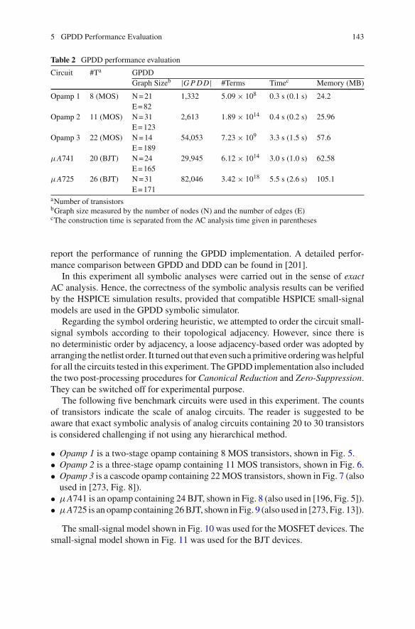
5 GPDD Performance Evaluation 143
Table 2 GPDD performance evaluation
Circuit #Ta GPDDGraph Sizeb |G P DD| #Terms Timec Memory (MB)
Opamp 1 8 (MOS) N = 21 1,332 5.09 × 10⁸ 0.3 s (0.1 s) 24.2E = 82
Opamp 2 11 (MOS) N = 31 2,613 1.89 × 10¹⁴ 0.4 s (0.2 s) 25.96E = 123
Opamp 3 22 (MOS) N = 14 54,053 7.23 × 10⁹ 3.3 s (1.5 s) 57.6E = 189
μA741 20 (BJT) N = 24 29,945 6.12 × 10¹⁴ 3.0 s (1.0 s) 62.58E = 165
μA725 26 (BJT) N = 31 82,046 3.42 × 10¹⁸ 5.5 s (2.6 s) 105.1E = 171
aNumber of transistorsbGraph size measured by the number of nodes (N) and the number of edges (E)cThe construction time is separated from the AC analysis time given in parentheses
report the performance of running the GPDD implementation. A detailed perfor-mance comparison between GPDD and DDD can be found in [201].
In this experiment all symbolic analyses were carried out in the sense of exactAC analysis. Hence, the correctness of the symbolic analysis results can be verifiedby the HSPICE simulation results, provided that compatible HSPICE small-signalmodels are used in the GPDD symbolic simulator.
Regarding the symbol ordering heuristic, we attempted to order the circuit small-signal symbols according to their topological adjacency. However, since there isno deterministic order by adjacency, a loose adjacency-based order was adopted byarranging the netlist order. It turned out that even such a primitive ordering was helpfulfor all the circuits tested in this experiment. The GPDD implementation also includedthe two post-processing procedures for Canonical Reduction and Zero-Suppression.They can be switched off for experimental purpose.
The following five benchmark circuits were used in this experiment. The countsof transistors indicate the scale of analog circuits. The reader is suggested to beaware that exact symbolic analysis of analog circuits containing 20 to 30 transistorsis considered challenging if not using any hierarchical method.
• Opamp 1 is a two-stage opamp containing 8 MOS transistors, shown in Fig. 5.• Opamp 2 is a three-stage opamp containing 11 MOS transistors, shown in Fig. 6.• Opamp 3 is a cascode opamp containing 22 MOS transistors, shown in Fig. 7 (also
used in [273, Fig. 8]).• μA741 is an opamp containing 24 BJT, shown in Fig. 8 (also used in [196, Fig. 5]).• μA725 is an opamp containing 26 BJT, shown in Fig. 9 (also used in [273, Fig. 13]).
The small-signal model shown in Fig. 10 was used for the MOSFET devices. Thesmall-signal model shown in Fig. 11 was used for the BJT devices.

144 7 Graph-Pair Decision Diagram
Fig. 5 Two-stage operational amplifier with compensation
Fig. 6 Three-stage amplifier with reversed nested Miller compensation
The simulator was compiled in the CYGWIN system [32] installed on a personalcomputer running Windows XP. The machine has an Intel Core2 Duo CPU at clockfrequency 2.26GHz and 1.93GB memory.
Shown in Table 2 are the collected performance data for the benchmark circuits.After substituting all transistors by their small-signal models, the small-signal circuitcomplexity can be measured by the converted graph size, i.e., the number of edges

5 GPDD Performance Evaluation 145
Fig. 7 Schematic of folded cascode
Fig. 8 Schematic of μA741

146 7 Graph-Pair Decision Diagram
Fig. 9 Schematic of μA725
s
mbgm
d
g b
s
RCgd
Cgs
R
R
bd
Rds
R
Cgb
bsC
bs
bd
Cd
g
Fig. 10 MOSFET small-signal model
(E) and the number of nodes (N). #T erms counts the number of product termsrepresented by a GPDD. In this experiment the number of terms was counted bylumping all parallel G-type edges in a converted graph.
It is important to notice that the GPDD algorithm without incorporating hierarchi-cal analysis was able to solve these benchmark circuits in a matter of a few seconds

5 GPDD Performance Evaluation 147
beπC
e
G π
Cμ
Go
cb
GmV
Fig. 11 BJT small-signal model
with the maximum memory around 100 MB. Moreover, the reader should notice thata total number of 3.42 × 10¹⁸ product terms were generated by the GPDD algorithmin about six seconds for the μA725 circuit. Remember that the total number of termsis a problem-specific invariant number that is independent of symbol order. A symbolorder could change the GPDD size, but does not change the total number of terms.
If we would like to explicitly print the sequence of all 3.42 × 10¹⁸ product termsto the console, it would probably take days. Storage of all such terms in sequenceand algebraic manipulations on them would encounter serious problems even using amost powerful desktop computer we have today. It is doubtless that symbolic analysisof a problem of such a complexity would not be possible without employing BDDas the core computation engine.
We finally remind that the symbolic GPDD construction time usually is muchgreater than one round of GPDD evaluation time. Unless the GPDD size is huge, inmost applications the numerical GPDD evaluation time is negligible comparing to theconstruction time. This is typical in most BDD-based implementations of symbolicanalysis tools.
6 A Discussion on Cancellation-Free
Those BDD-based symbolic construction methods could run into the term-cancellation problem. Although BDD-based term evaluation does not expand theterms represented by the BDD 1-paths, the existence of cancellation could poten-tially lead to numerical errors. The reason is that those analytically perfectly canceledterms are not exactly canceled in numerical evaluations, thus resulting in accumulatedroundoff errors [201]. We use a simple example to illustrate the issue of cancellation.
Consider the circuit shown in Fig. 12 containing two stages of RC elementsdenoted by G1, G2, G3, and G4. It is driven by an input current source Iin and thevoltage at node ‘3’ is measured for output Vout = V3.
The MNA formulation of the circuit is given by

148 7 Graph-Pair Decision Diagram
Fig. 12 A two-stage RCcircuit 1
0
2
Iin
Vout
3G1 G3
G2G4
⎢
⎣G1 −G1 0
−G1 G1 + G2 + G3 −G30 −G3 G3 + G4
⎤
⎥
⎢
⎣V1V2V3
⎤
⎥ =⎢
⎣Iin
00
⎤
⎥ . (7)
The DDD program [196] would treat the coefficient matrix symbolically as follows
A =⎢
⎣a b 0c d e0 f g
⎤
⎥ , (8)
where each symbol stands for a nonzero entry defined by: a = G1, b = c = −G1,d = G1 + G2 + G3, e = f = −G3, and g = G3 + G4. We call such symbolscomposite symbols, meaning that they are composed by the primitive circuit deviceparameters. We see obviously that some identical matrix entries are denoted bydistinct symbols. Therefore, we may expect term cancellation when the determinantis expanded.
The determinant det(A) can expanded into product terms as det(A) = adg −ae f − bcg. When the composite symbols are further expanded into the primitivecircuit parameters, we shall see product term cancellation as follows:
det(A) = adg − ae f − bcg (9)
= G1(G1 + G2 + G3)(G3 + G4) − G1G23 − G2
1(G3 + G4) (10)
= G1G2G3 + G1G2G4 + G1G3G4. (11)
The terms listed above tell us one critical difference between DDD-based and GPDD-based evaluations. The DDD evaluates terms as written in (10), while the GPDDevaluates terms as written in (11). Although both expressions are equal, they are notnumerically equal due to the roundoff errors. When the number of terms reachesa level of 1010 or higher, the roundoff numerical error is significant. Typically, thecancellation-free evaluation is more accurate [201].
In some applications cancellation could create a serious problem. For exam-ple, in interval based approximate analysis of circuit variations, each subexpressionwould be evaluated in approximation [78]. Then two analytically canceling termsT1 − T2 = 0 would generate a large error when the terms T1 and T2 are evaluated by

6 A Discussion on Cancellation-Free 149
different approximations. Such errors are accumulated in the bottom-up evaluationsperformed in BDD, causing excessive errors in the end.
To avoid the cancellation problem inherent in DDD, Tan et al. [231] proposed a de-cancelation strategy to make a DDD cancellation-free by post-processing DDD. Sucha makeshift strategy entails extra computational cost, and in addition the proposedimplementation is not straightforward.
In contrast the two-graph-based GPDD construction method guarantees thecancellation-free property [204], although its construction cost could be slightlyhigher than DDD because of a higher dimension of the problem caused by directlyprocessing the network branches, instead of the lumped nodal admittances.
The GPDD method analyzes the circuit of Fig. 12 by constructing a pair of graphsfrom the circuit, with the element branches becoming the graph edges. After a GPDDis constructed, those reduction paths would generate the following product terms thatsum up to zero,
− G1G3 X + G1G2G3 + G1G2G4 + G1G3G4 = 0, (12)
where X = Iin/Vout models the input-output. The symbolic transfer function derivedfrom (12) is cancellation-free.
In addition to being cancellation-free, another feature of GPDD is that the sym-bolic expression is directly composed of the primitive circuit parameters, instead ofcomposite symbols. This property can be particularly valuable in sensitivity analysis.
For example, we would like to compute the sensitivity of the transfer function withrespect to a circuit parameter, say, G3. DDD would have to apply the differential chainrule to the symbolic expression in (9),
∂ det(A)
∂G3= a
∂d
∂G3g + ad
∂g
∂G3− a
∂e
∂G3f − ae
∂ f
∂G3− bc
∂g
∂G3
= G1G2 + G1G4,
where the last expression again results from canceling many terms. In contrast, thesensitivity computation by GPDD is straightforward [206]. In general, if the originalsymbolic construction has term cancellation, the resulting constructs for sensitivitywould also involve cancellation. For applications requiring numerical accuracy, acancellation-free algorithm like GPDD is recommended.
7 Summary
This chapter has presented an alternative BDD-based symbolic circuit analysismethod based on the generalized two-graph method. A pair of graphs are createdand reduced is edge-pairs, and in the reduction course all sharable graph-pairs aresaved in a hash table managed with a BDD. The constructed GPDD data structure

150 7 Graph-Pair Decision Diagram
is a symbolic computation engine for the AC response. Several key features makethe GPDD symbolic representation more advantageous than other representations.For example, the product terms in GPDD are cancellation-free, which is beneficialto numerical accuracy. Another advantage of GPDD is that the symbols involved aredirectly the small-signal circuit parameters, which brings up much convenience forthe post-processing tasks in symbolic analysis. For example, a graphical user inter-face developed on GPDD could be very efficient. Also, symbolic sensitivity analysisis much easier to implement on a GPDD. We further expect that the GPDD could bea good means for developing incremental symbolic analysis algorithms.
The reader should be aware that great room exists for further improving the imple-mentation of the GPDD algorithm. The efficiency of a BDD-based implementationgreatly depends on facts such as symbol ordering, hash table design, and constructionstrategy (whether using depth-first, breadth-first, or parallel construction, etc.) Theseissues are worth attempting in other innovative implementations.
For analog circuits larger than the scale considered in this Chapter, the GPDD algo-rithm would still encounter difficulty. In that case hierarchical analysis by dividingand conquer is a popular strategy. The GPDD-based hierarchical analysis methodswill be addressed in Chap. 8.

Chapter 8Hierarchical Analysis Methods
1 Introduction
BDD-based symbolic analysis is a powerful technique, capable of solving muchlarger analog circuits by exact analysis (i.e., without applying approximation). How-ever, the extension of solvability is still limited by the circuit size. In general, thecomplexity of BDD-based analysis (i.e., the BDD size as a function of the prob-lem size) still grows exponentially, but the growth rate could be much lower than anon-BDD-based method [199]. When circuit size exceeds the maximum capabilityof a BDD-based implementation by flat (i.e., non-hierarchical) analysis, hierarchicalanalysis strategies must be used.
Many hierarchical symbolic analysis methods have been proposed in the literatureso far since 1980, such as [70, 80, 81, 118, 153, 219, 255, 256, 273] among others.Those methods can be classified into two categories, depending on whether the circuitpartitioning is based on the circuit itself or a matrix representation (typically an MNAmatrix). Although there exist direct connections between a matrix representation andits corresponding circuit structure, the implementation details of the two classes ofmethods could be drastically different. There also exist many graphical methods forsolving linear matrix equations such as the signal flow graph (SFG) method and theCoates graph method [117]. We subsume those graphical methods derived from thematrix representations of a circuit into the category of matrix-based methods as well.In this sense, by the first category we mainly refer to those methods based on puretopological processing of a circuit such as by enumerating spanning trees of onegraph or a pair of graphs.
Those traditionally developed hierarchical methods mainly took the forms ofsequence of expressions (SOE). If structural regularity or loose coupling betweenblocks is identifiable in a circuit, generating SOEs is a relatively simple task. Thedifficulty could arise from most analog integrated circuits that are less regular ordensely coupled [273]. For such cases, those SOE based hierarchical methods wouldhave to require more complicated nesting of symbolic expressions, causing higherconstruction complexity and worse numerical stability.
G. Shi et al., Advanced Symbolic Analysis for VLSI Systems, 151DOI: 10.1007/978-1-4939-1103-5_8,© Springer Science+Business Media New York 2014
152 8 Hierarchical Analysis Methods
Although not all analog circuits are loosely connected, most of them do involvesimilar or sometimes identical subcircuits. A hierarchical analysis method shouldexplore such circuit-level structures to create efficient symbolic constructs in hier-archical forms. BDD-based analysis methods are highly suitable for managing suchcircuit-level regularity. The hierarchical analysis methods developed in this chapterare specifically targeted toward highlighting the advantages of BDD in hierarchi-cally managing such circuit-level regularity and interconnections. It is important tobe aware that the structural information at the circuit-level is most relevant to thedesign automation of analog integrated circuits. Hierarchical methods taking struc-tural circuit hierarchy into consideration are important for both circuit analysis andcircuit synthesis, with the latter including generation of network topology and cellbehavioral models.
This chapter is organized as follows. An overview on the existing hierarchicalsymbolic methods is made in Sect. 2, where we explain several typical methods forgenerating SOEs, such as the Gaussian elimination method and the Schur decom-position method. Then in Sect. 3 we introduce a basic notion called symbolic stampthat has become a standard means for exploring the circuit-level regularity and con-structing hierarchical strategies. We then point out that both DDD and GPDD aregood optional methods for generating shared symbolic stamps for multi-port circuitblocks. Symbolic stamps can be incorporated directly in both MNA-based analysis ormultiport GPDD based analysis. As an extension of the GPDD method, we developin Sect. 4 a new graph reduction rule for handling multiport modules described bymulti-input multi-output (MIMO) symbolic stamps. Then in Sect. 5 we present twohierarchical analysis strategies by applying DDD and GPDD for the management ofsymbolic stamps. The first strategy is called GPDD+DDD, by which the symbolicstamps are built by GPDD, and all such stamps are assembled into an MNA matrix,which is then analyzed by a DDD program. The second strategy is called HierGPDD,which employs pure graphical partitioning of circuit and performs analysis solelyby GPDD from one level to another. The second strategy can be implemented byDDD as well, therefore, we compare the two implementations in experiment. Theexperimental evaluations and comparisons of the proposed strategies are presentedin Sect. 6. Section 7 concludes the chapter.
2 Existing Hierarchical Methods
Research on hierarchical symbolic analysis began in the 1980s when the designautomation needs of analog integrated circuit attracted many researchers’ attention[80, 219]. The main techniques developed during the early years were mainly bygenerating nested SOEs. In this section we make a brief review on those representativehierarchical techniques proposed in [39, 70, 81, 82, 219, 231, 236].

2 Existing Hierarchical Methods 153
Starzyk and Konczykowska [219] proposed in 1986 a hierarchical analysis methodby Coates flow-graph. The Coates flow-graph method developed by Coates in 1958[29] is a topological method for solving linear algebraic equations. The matrix ele-ments are represented by the weighted directed edges in a flow-graph. The determi-nants appearing in the Cramer’s rule are calculated by enumerating k-connectionsfrom a flow-graph. That is, the product terms of a determinant are enumerated fromthe disjoint loops in a Coates graph. The Coates flow-graph method is basically anexhaustive enumeration method in that all such k-connections and loops must beexplicitly enumerated. When a circuit gets large, the complexity of direct enumera-tion could be prohibitive, because sharing is not considered. In the work [219] onlya few relatively simple analog filter circuits containing ideal opamps were consid-ered in application, which could not demonstrate the competitiveness of the Coatesflow-graph method.
Hassoun and McCarville [82] proposed in 1993 another hierarchical analysismethod by applying Mason’s signal flow graph (SFG) method. It is well-known thatMason’s rule for solving SFG also requires exhaustive enumeration of paths andloops, whose complexity is comparable to that of the Coates flow-graph method.Also, the work [82] only made experimental tests on small and loosely connectedcircuits.
Hassoun and Lin [81] proposed in 1995 an improved hierarchical method basedon circuit partitioning. A full MNA matrix is created first, then transformed byGaussian elimination to a matrix called Reduced Modified Nodal Analysis (RMNA)matrix, whose entries are in SOEs. By this method, two connected circuit blockscan be merged by eliminating the joining nodes. This method is valid in principle,however, it failed to consider the numerical difficulties it might encounter. Gaussianelimination involves divisions in the nested expressions, hence numerical stability isa problem during the numerical evaluation phase.
Several years later, Pierzchala and Rodanski published the work [153] in 2001 bypointing out that it is unnecessary to establish SOEs via hierarchical decomposition.Instead, they proposed a direct symbolic Gaussian elimination method by succes-sively reducing a full MNA matrix into a two-port matrix. In essence, this methodstill belongs to the category of Gaussian elimination, by which the ultimately gen-erated two-port matrix consists of entries in symbolic SOEs. To control the negativeeffect of fill-ins, the authors proposed a local pivoting scheme to reduce the num-ber of symbolic operations. As with all Gaussian elimination methods, no effectivestrategy could be proposed for handling the numerical stability problem during theeliminations. The post-scaling technique discussed by Pierzchala and Rodanski foralleviating the numerical division problem could only partly solve the problem withquite high cost.
The work published by Doboli and Vemuri [39] in 2001 explored structural inter-connection regularity existing in many analog integrated circuits. They noticed theexpression-level regularity that could result from the Gaussian elimination of internalnodes when two blocks are interconnected. However, the efficiency of such a strategy
154 8 Hierarchical Analysis Methods
requires a regularity extraction tool, whose development was not fully addressed inthat work (and in fact would not be trivial). On the other hand, how to efficientlymanage common subexpressions as the result of circuit regularity exploration alsowas not addressed in that work.
In 2002 Guerra et al. [70] proposed an approximate hierarchical method by circuitreduction. The approximation is created by using the two-graph method to gener-ate dominant symbolic terms, which are identified by a technique called weightedintersections of matroids proposed in [256]. Hierarchically generating dominantterms would require reliable error control to prevent the trimming error from growing.Typically, heuristic error controls are employed. By approximate analysis, the pro-posed method was able to analyze relatively larger analog circuits. One experimentalcircuit reported in [70] contains 83 MOS transistors.
Although symbolic approximation by retaining dominant terms can help generateinterpretable symbolic results, it has several limitations. For example, its symbolicresult depends on the circuit biasing condition. A more serious limitation of approxi-mate symbolic results is that they cannot be used for calculating sensitivities, becausetruncation could severely break down the accuracy of gradients. For these reasons, weshall not compare the exact hierarchical analysis methods developed in this chapterto any approximate analysis methods.
Since the proposal of DDD, the authors of DDD have applied this novel datastructure to hierarchical analysis as well [231, 236]. They have attempted severalideas; the main idea was by Schur decomposition of an MNA matrix. Simply speak-ing, a large MNA matrix is built first for a whole circuit, then it is partitionedinto block submatrices with loose couplings. The lower-dimensional block matricesresulting from Schur decomposition are analyzed by the DDD program. Since thepartitioned matrices have lower dimensions, the DDD construction complexity isreduced greatly, although several rounds of DDD runs are required. Moreover, themultiple DDDs (i.e., the so called cofactors) resulting from the multiple runs must bewell managed for efficiency in post-processing. However, the main limitation of theDDD-based hierarchy is that the resulting symbolic expressions are in nested form,which could involve a large amount of canceling terms. We also point out that theSchur decomposition strategy can equivalently be described in the form of symbolicstamps, which is much easier to understand and to construct in a divide-and-conquerway.
2.1 Symbolic Analysis in SOE
For some special circuits, such as the sequential ladder shown in Fig. 1, generatinga symbolic solution in SOE is easy. Using the variables introduced in the circuit, wecan write the following voltage–current relations [118]:

2 Existing Hierarchical Methods 155
3
in
Z6
Y5
Z2
Y1Y3
Z4
v6 v2
v4
i4i6 i 2
i5
v5
Vout
ii13
vv1
V
Fig. 1 A three-section ladder circuit
Z4Z6 1i2i4
v5
0
Vini6 v3 v1
Z2Y5 Y3 1Y
Fig. 2 BDD representation of the expressions in (1)
v1 = Vout = 1Vi2 = Y1v1v3 = v1 + Z2i2i4 = i2 + Y3v3v5 = v3 + Z4i4i6 = i4 + Y5v5
Vin = v5 + Z6i6H = Vout
Vin= 1V
Vin.
(1)
Except for the last expression, all the rest expressions in (1) are written in multiply-and-add form without divisions. One may expand these expressions into sum-of-product (SOP) forms, but it is not necessary for symbolic computation. Nested expres-sions have the advantage of reducing the number of expressions. However, such SOEswithout division are available only for very special circuits that are sequentially con-nected. In general, the symbolically generated SOEs would be more complicated andinvolve divisions.
It is easy to see that the nested sequential expression (1) in multiply-and-addform can directly be converted into a BDD shown in Fig. 2, where the solid arrowsperform multiplications and the dashed arrows perform additions. In principle, anylinear circuit can be solved in symbolic SOEs or SOP terms. However, the generationalgorithms are drastically different. The key difference between SOEs and SOPterms is whether or not divisions are involved. The arithmetic operations in SOEswould involve divisions in general, which has the disadvantage of possibly beingdivided by small numerical values if no numerical reference values are used in thegeneration process. To avoid divisions, usually an algorithm for generating SOP mustbe employed.

156 8 Hierarchical Analysis Methods
2.2 Gaussian Elimination Method
SOEs are most easily generated by the Gaussian elimination method, for which weillustrate by a 3 × 3 matrix. Let the LU factorization be given as follows
⎡a11 a12 a13a21 a22 a23a31 a32 a33
⎢
⎣ =
⎡1
α21 1α31 α32 1
⎢
⎣
⎡u11 u12 u13
u22 u23u33
⎢
⎣ . (2)
The Gaussian elimination is performed by a sequence of regular expressions givenby
a(k+1)i,j = a(k)
i,j − a(k)i,k
a(k)k,k
· a(k)k,j (3)
where the superscript (k) indicates the elimination step and a(1)i,j = ai,j for i, j ≥
k + 1. The factor a(k)i,k/a
(k)k,k is a multiplicative elimination factor that involves a
division. Whether the divisor a(k)k,k is small or not is not a concern during the symbolic
generation phase. However, it matters during the numerical evaluation phase. Thenumerical error caused by dividing a small a(k)
k,k could propagate to the subsequentsymbolic evaluations, causing accumulated numerical errors.
The symbolic LU factorization generates SOE entries in the upper and lowertriangular matrices U and L in (3). When the bottom-level symbols are substituted bytheir numerical values, the entries in the LU factorization are successively evaluated.After that, the forward and backward substitutions are executed to solve y fromLy = b and x from Ux = y, respectively. The complexity of Gaussian elimination ofann×n dense matrix is known to be O(n3), i.e., of the cubic polynomial complexity.For sparse matrices arising from circuits, the complexity of symbolic factorizationcould be reduced by appropriate pivoting [153].
Although straightforward, the SOE generation method by Gaussian eliminationhas the following disadvantages:
• SOEs involve divisions in general, which are the main source of numerical errorsduring the numerical evaluation phase. In the sense of pure symbolic analysis, itis impossible to implement numerical pivoting during symbolic Gaussian elimi-nation.
• Post-processing of nested SOEs with divisions might generate lengthier expres-sions involving more divisions, worsening the numerical stability. (A typicalexample is in sensitivity analysis.)
• Performing s-expansion based on SOEs would be hard. However, symbolicpole/zero analysis normally requires generation of transfer functions in s-expanded(or s polynomial) forms.
The limitations listed above remind us that the Gaussian elimination method is notthe most favorable method for practical applications; this fact was also pointed out by

2 Existing Hierarchical Methods 157
Yu and Sechen in [273]. In contrast, a BDD-based symbolic analysis algorithm couldgenerate SOP symbolic representations without divisions, and by a proper construc-tion its complexity is much lower than by brute-force enumeration. For example, thetransfer function of a 20-section RC ladder circuit would involve 1.66 × 10⁸ SOPterms. However, such a transfer function could be represented by a GPDD with only120 vertices with a good symbol order. Such a compactness would not be possiblewithout taking into account of sharing all common subexpressions. However, noneof the published SOE-based methods have considered the matter of subexpressionsharing.
An another example, shown in Fig. 3 is a band-pass filter [219]. By assuming allopamps ideal, a reasonable symbol order leads to a GPDD of 498 vertices, whichrepresents more than 1.9 × 10⁸ SOP terms. BDD-based expressions are SOEs aswell, but are managed by maximized sharing.
2.3 Schur Decomposition with DDD
Since the proposal of DDD, several hierarchical analysis techniques based on DDDhave been attempted. One technique is derived from Schur decomposition, whoseprinciple is explained here. Suppose the MNA formulation of a flat circuit is describedby the following partitioned equation
⎤A11 A12A21 A22
⎥ ⎤x1x2
⎥
=⎤
b1b2
⎥
(4)
where Aij (i, j = 1, 2) are block matrices, and xj and bi are respectively the parti-tioned unknown vectors and the right-hand side vectors of compatible dimensions.Assume that none of the unknowns in x1 belong to the output variables and all inputsources are included in b2 (implying that b1 = 0). Assume that A11 is invertible.Then, application of Schur decomposition transforms the block matrix equation (4)to ⎤
A11 A12
0 A22 − A21 A−111 A12
⎥ ⎤x1x2
⎥
=⎤
0b2
⎥
. (5)
It follows that for I/O response, we only need to solve the reduced dimensionalequation ⎦
A22 − A21 A−111 A12
)x2 = b2. (6)
However, solving this matrix equation requires solving the reduced dimensionalmatrix Y2 := A21 A−1
11 A12 first.The submatrix A21 A−1
11 A12 can be solved in two steps: Firstly solve the columnsof V1 from A11V1 = A12, then compute Y2 = A21V1. Note that in general the sub-matrix A12 has multiple columns and A21 has multiple rows. Hence, Y2 is essentially

158 8 Hierarchical Analysis Methods
VoutG37
G39
13
G38 G40
Vin G5 G72 3
G6
C6C8
G1
G2
1
G4
G3
G9
1012 11
C35C33
G33
G34 G32
G31
G29
G28G30
G36
G19
G20
G21
7 8 9
G27G22
G23
G24
C24
G25
C26
456
G10
G11
G12
G13
G14
G18
G15
C15
G16
C17
Fig. 3 A band-pass filter

2 Existing Hierarchical Methods 159
the admittance matrix of a multi-port circuit block, with the columns of A12 charac-terizing the input ports and the rows of A21 the output ports. Hence, in this sense, thematrix Y2 is just an admittance stamp for that multiport. Combining this multiportstamp with the rest of the circuit described by the submatrix A22 gives the wholecoefficient matrix in Eq. (6). A direct consequence of circuit partitioning is that thematrix solves can deal with lower dimensional matrices, which can significantlyreduce the symbolic analysis complexity.
The reduced dimensional matrix of the lower-right block becomes A22 :=A22 − A21 A−1
11 A12, The multiport stamp Y2 := A21 A−111 A12 can be constructed by a
symbolic program such as DDD. In the work by Tan and Shi [236] published in 2000,the matrix of A−1
11 A12 was solved by the DDD solver by considering the columnsof A12 as the multiple RHS vectors. While multiple RHS vectors are involved, theleft-hand side matrix A11 is common to all the linear solves. Hence, it is only neces-sary to construct those required cofactors of the matrix A11 by saving them in sharedform in a DDD [236].
It appears that applying DDD directly to Schur decomposition of a coefficientmatrix is equivalent to the creation of a symbolic multiport stamp. However, differ-ent perspectives could result in different implementation details. Specifically, matrix-based direct Schur decomposition only considers matrix-level structure, which mighthave missed some circuit-level regularity that could be taken advantage of. For exam-ple, some subcircuits in a circuit could be fully identical. A small-signal model for alltransistors in a circuit is such a case. Whenever two subcircuits are totally identical,we only need to create one symbolic stamp for both subcircuits. Identifying suchcommon subcircuit blocks from an already created MNA matrix is a less trivial task.In this sense, the notion of symbolic stamp is more oriented toward circuit topologybased hierarchical analysis. We shall further discuss the symbolic stamp constructionissue in Sect. 3.
Later, the authors of another work [231] made extra effort on avoiding explicit useof intermediate variables. The proposed method applies the following determinantdecomposition identity (assuming A11 is nonsingular),
∣∣∣∣A11 A12A21 A22
∣∣∣∣ = ∣
∣A11∣∣∣∣A22 − A21 A−1
11 A12∣∣ , (7)
which is equivalent to
∣∣A22 − A21 A−1
11 A12∣∣ =
∣∣∣∣A11 A12A21 A22
∣∣∣∣/
∣∣A11
∣∣. (8)
This identity tells us that the determinant∣∣A22 − A21 A−1
11 A12∣∣ can be computed by
the division of the full matrix determinant
∣∣∣∣A11 A12A21 A22
∣∣∣∣ and the submatrix determinant
∣∣A11
∣∣. A procedure called de-cancellation was proposed in [231] to reconstruct a
DDD for the full matrix by algebraically operating (multiply and add) on the DDD

160 8 Hierarchical Analysis Methods
factors and complementary factors created for the matrix A11. We should point outthat this reversed DDD construction process is not equivalent to the direct DDD con-struction for the full determinant
∣∣A22 − A21 A−1
11 A12∣∣ due to the possibly different
symbol orders involved implicitly.The work [231] reported that some circuits (like μA725) once unsolvable by a flat
DDD could be solved by the de-cancellation procedure. The de-cancellation proce-dure has demonstrated a fact that a DDD could also be constructed by “augmenting”
a smaller matrix to a larger matrix. Algebraically, the full matrix
⎤A11 A12A21 A22
⎥
can be
considered an augmented formulation of the computation of⎦
A22 − A21 A−111 A12
).
A further discussion in this regard is omitted. An extension of the de-cancellationmethod to approximate analysis of large interconnect networks was developed in[229].
3 Symbolic Stamp Construction
The notion of symbolic stamp has been implicitly used in the literature in a varietyof forms; for example, the concept of Reduced MNA (RMNA) matrix used in [81],the concept of circuit regularity introduced in [39], and others in the form of Schurdecomposition. This notion can be presented explicitly in transadmittance matrixform representing a multiport circuit block.
The symbolic stamp for a multiport circuit block is defined as a multi-dimensionalVCCS element described by
⎛
⎧⎪
i1...
i2
⎨
⎩⎠ =
⎛
⎧⎪
y1,1 · · · y1,m...
. . ....
ym,1 · · · ym,m
⎨
⎩⎠
⎛
⎧⎪
v1...
vm
⎨
⎩⎠ , (9)
in which the coefficient matrix (denoted by Y ) is an m × m admittance matrix (orcalled Y -matrix). Anm-port module can be described bym2 transadmittance entries,yi,j , i, j = 1, . . . , m, each of them is a symbolic function of the circuit parametersof the module. When this module is inserted into a higher-level circuit, them2 entriesbecome the intermediate variables in the hierarchy.
Symbolic stamps can be created by using either a DDD or GPDD program thatcreates symbolic representation with sharing. Notice that each entry yk,j of the sym-bolic stamp matrix Y has a circuit interpretation; namely, it is calculated as the outputcurrent flowing through the short-circuited kth port when all the m ports but the jthport are short-circuited, and the jth port is connected with a unity voltage sourceas the input. Ranging the indices (k, j) over k, j = 1, . . . ,m with the correspond-ing port connections, we obtain a set of m2 currents, giving the m2 entries of thematrix Y .

3 Symbolic Stamp Construction 161
If we assume that all ports are referenced to the ground, the unity voltage at theith port is applied between the ith port terminal and the ground, while all the restterminals are short-circuited to the ground. The currents flowing through all portsare directed from the ground to the port terminals.
3.1 Symbolic Stamp by Multiroot DDD
DDD is an MNA matrix-based symbolic solver by applying the Cramer’s rule. LetAx = b be an MNA formulation, where b stands for the RHS vector includingthe applied sources. For input–output analysis, typically only one or two unknownstate variables inside x need be solved. As the input-output pair varies, the coeffi-cient matrix A is updated slightly to account for the port change. Meanwhile, theb vector and the unknown variables vary accordingly. However, the majority of Aentries remain unaffected. Consequently, a DDD-based construction can automat-ically share most of the existing cofactors of A. Hence, using DDD for symbolicstamp construction saves quite an amount of memory.
In principle, DDD is an optional candidate for constructing symbolic stamps.However, several issues with this method are worth mentioning. Firstly, as we havepointed out, all nonzero MNA matrix entries are treated as distinct DDD symbols,including those constant entries like 1 or −1 that frequently appear in MNA formu-lations. Such constants not only occupy memory, but also consume CPU resource,hence it is wasteful to process constants as variables. Secondly, identical matrixentries (but appearing at different locations in matrix) are treated as different sym-bols in DDD. Such entries also frequently appear in MNA formulations. Thirdly, theDDD symbols are not primitive circuit elements, rather they are lumped incidenceadmittances to nodes. Hence, the DDD symbol encoding method is the major causeof the term cancellation problem in numerical evaluation. The reader should be awareof these limitations when applying DDD for symbolic stamp construction.
3.2 Symbolic Stamp by Multiroot GPDD
Since the matrix stamp entry yk,j is the current flowing through the kth port inresponse to a unity voltage excitation at the jth port (with the rest ports short-circuited), each yk,j corresponds to a specific circuit graph by which a GPDD can beconstructed. GPDD solves a transfer function as one of the four dependant sources,i.e., VCVS, CCCS, VCCS, and CCVS. Since the admittance matrix entry yk,j isdefined as a VCCS, it is solved by GPDD as a CCVS (inverted), by letting the short-circuited port k (CC) control the open-circuited port j (VS) (see [201] or Chap. 7).
It is obvious that the m2 transfer function entries yk,j (k, j = 1, . . . ,m) arenot totally independent. For example, y1,j , j = 1, . . . ,m, correspond to m transferfunctions having the first port as the output and one of the m ports as the respectiveinput port. The linear mapping from m inputs to m outputs can be represented by a

162 8 Hierarchical Analysis Methods
R
1
R
1
R
1
R
1
Ry
y
12
22
y
y
11
21
i2
V1
V2
i1
Fig. 4 A two-port resistor block and its stamp
shared GPDD with m2 roots (called a multiroot GPDD), each generating one entryyk,j . The construction procedure is described next.
Since all initial graphs for creating a multiroot GPDD are created from the samecircuit module by selecting specific ports, it is natural to select a fixed symbol orderfor all GPDD constructions (with the exception that the I/O symbol must alwaysbe placed at the roots, i.e., the leading position). On the other hand, since all initialgraphs differ only slightly, numerous intermediate graph-pairs generated during thegraph-pair reduction process are likely to be identical, hence can be shared [216, 264].We only need to use one hash table throughout the multiroot GPDD construction.Sharing the m2 symbolic entries yk,j all together in a single multiroot GPDD cansave both memory and CPU time during construction.
In practice, it is inevitable that the construction complexity would grow expo-nentially with the number of ports. Hence, while partitioning a circuit, we shouldintentionally break up the circuit blocks at the sparse connections. It is suggested tochoose a port number m ≤ 4 for reasonable efficiency.
A prominent feature of GPDD is that the primitive circuit parameters are directlythe GPDD symbols. There do not exist symbols of constant values or identical ele-ments encoded as distinct symbols like in DDD. Such direct one-to-one mappingbetween circuit element and symbol brings forth many advantages as we have men-tioned several times (see Chap. 7).
The GPDD symbolic stamp construction is illustrated by a simple example below.Let the admittance matrix of a two-port network be
(i1i2
)
=(y11 y12y21 y22
) (v1v2
)
. (10)
We need to compute symbolically the four transadmittance functions yij , i, j = 1, 2.The jth column of the admittance matrix Y can be computed as follows: Connect aunity voltage at one port and short the other, measure the currents at both ports toobtain y1j and y2j .
We illustrate the GPDD symbolic stamp construction by a two-port description ofa single resistor shown in Fig. 4. The transadmittance matrix is shown aside in Fig. 4.The four entries in the stamp will be generated by four runs of the GPDD routine.
GPDD computes one transadmittance by superimposing a specified input and out-put pair to the graphical circuit representation. Shown in Fig. 5a, b are the respective

3 Symbolic Stamp Construction 163
(a)
(b)
Vs Vs
Cc Cc
Vs VsCc Cc
V
V
Fig. 5 The graph-pair reduction processes for the single resistor circuit. a GPDD construction fory11. b GPDD construction for y12
graph reduction processes for the two entries y11 and y12. For y11, the I/O is a self-controlled CCVS applied at port 1, which in Fig. 5a is seen as two cascaded edgesCC and VS. For y12, the edge representation for I/O is a mutual CCVS, with CCplaced at port 1 and VS at port 2, see Fig. 5b.
Since the four transadmittances come from the same circuit with only slightdifference in the port connections, many subgraphs generated from reduction can
164 8 Hierarchical Analysis Methods
be shared. For example, by reversing the solid-arrow sign attached to vertex “R”in Fig. 5b, the two “R” vertices in the two GPDDs can be shared. The details areimplementation dependent.
4 Reduction Rule for Multiport Element
With a symbolic stamp established for a multiport block, both DDD and GPDDcan be used to create higher level symbolic expressions by combining the multiportstamp. Comparatively, the DDD method is a little more straightforward than theGPDD method, because a multiport stamp is already in matrix form, which is easyto be embedded into a larger MNA matrix. However, by using the GPDD methodat one level higher, we need to convert the matrix stamp into a graphical form forgraph reduction; that means we need to introduce additional graph reduction rulesfor dealing with a multi-dimensional VCCS element. It turns out that the new rule isjust a simple extension of a two-port dependent element.
The extension is based on the basic superposition principle; that is, each outputis a sum of m VCCS elements. Specifically, the kth equation in the stamp consistsof m voltage-controlled currents
ik = yk,1v1 + yk,2v2 + · · · + yk,mvm. (11)
We may denote each current in the right-hand side by ik,j = yk,jvj . The Eq. (11) isnothing else than a current controlled by m voltages.
The linear multiple dependence can be represented by graph edges with crossdependence, with all such edges placed at the corresponding port terminals. Thenapply the previously developed pairwise graph-reduction rules to those externallyplaced port edges.
Note that the m2 entries in the m-dimensional symbolic stamp lead to m2 two-port VCCS elements, i.e., ik,j = yk,jvj . Hence, we have to place m CS edges to thekth port, meanwhile place m VC edges at all m ports. On the other hand, since eachvoltage vj controls m port currents ik,j for k = 1, . . . ,m, we have to duplicate thevoltage vj by m times at the jth port to create m controlling voltage edges denotedby vk,j . Since the duplicated edges are all connected in parallel, we have vk,j = vjfor all k, j = 1, . . . ,m.
Speaking in terms of graph edges, decomposing one current ik at port k into mpartial currents is equivalent to placing m parallel current edges with the total currentik. The net result is that the m-dimensional stamp has been decomposed into m2
two-port VCCS elements, denoted by ik,j = yk,jvk,j , in the graphical representation.For V Ck and C Sk placed at the same port, the kth VCCS element is just an
admittance element, hence the two edges can be merged into a single admittance(Y-type) edge with weight yk,k.
In summary, the edge allocation rule stated above simply transforms an m-portVCCS element into (m2 − m) regular VCCS elements (corresponding to those

4 Reduction Rule for Multiport Element 165
Fig. 6 Edge-pairs for a three-port module. Two voltageedges v1,2 and v3,2 are addedto port 2
1 32
0 0 0
i1,2
i3,2
v1,2
v3,2
y1,1
y2,2 y
3,3
1
0
y1,1
i1,2
v2,1i
1,3
v3,1
3
0
y3,3
v1,3
v2,3
i3,1
i3,2
2
0
v1,2
v3,2
i2,1
i2,3
y2,2
Fig. 7 Complete edge allocation for a three-port module. Five edges are placed at each port
off-diagonal stamp entries) and m port admittance elements (corresponding to thosediagonal stamp entries). As a result, (m− 1) parallel voltage edges, (m− 1) parallelcurrent edges, and one admittance edge must be introduced at each port.
We illustrate the edge placement rule for a three-port symbolic stamp, whoseY -matrix is defined by
⎛
⎪i1i2i3
⎨
⎠ =⎛
⎪y1,1 y1,2 y1,3y2,1 y2,2 y2,3y3,1 y3,2 y3,3
⎨
⎠
⎛
⎪v1v2v3
⎨
⎠ . (12)
It involves three port currents defined by ik = yk,1v1 + yk,2v2 + yk,3v3 fork = 1, 2, 3. Each port current ik is composed of three partial currents denotedby ik,j := yk,jvj for j = 1, 2, 3. Let j = 2. We know that v2 controls three par-tial currents i1,2, i2,2, and i3,2. Hence, we need to place three VC edges at port 2,named by v1,2, v2,2, and v3,2 (all equal to v2). Now we have three VCCS pairs,i1,2 = y1,2v1,2, i2,2 = y2,2v2,2, and i3,2 = y3,2v3,2, among them the second oneis just an admittance element. Hence, the two edges i2,2 and v2,2 at port 2 can bemerged and replaced by an admittance edge y2,2 (see that shown in the middle ofFig. 6). As illustrated in Fig. 6, the edge v1,2 at port 2 controls the current i1,2 at port1, while the edge v3,2 at port 2 controls the current i3,2 at port 3.
Shown in Fig. 7 is the complete port edge allocation for the three-port module.Assuming that all ports are referenced to the ground (node 0), we see in the figurethat each port has five edges, including two controlling voltage edges, two con-trolled current edges, and one admittance edge, with their cross-dependence alreadyexplained.
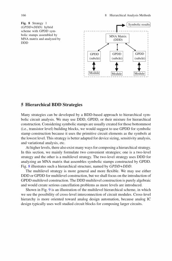
166 8 Hierarchical Analysis Methods
Fig. 8 Strategy 1(GPDD+DDD): hybridscheme with GPDD sym-bolic stamps assembled byMNA matrix and analyzed byDDD
Module
MNA Matrix(DDD)
(subckt) (subckt) (subckt)GPDD GPDDGPDD
Symbolic results
Module Module
5 Hierarchical BDD Strategies
Many strategies can be developed by a BDD-based approach to hierarchical sym-bolic circuit analysis. We may use DDD, GPDD, or their mixture for hierarchicalconstruction. Considering symbolic stamps are usually created for those bottommost(i.e., transistor level) building blocks, we would suggest to use GPDD for symbolicstamp construction because it uses the primitive circuit elements as the symbols atthe lowest level. This strategy is better adapted for device sizing, sensitivity analysis,and variational analysis, etc.
At higher levels, there also exist many ways for composing a hierarchical strategy.In this section, we mainly formulate two convenient strategies; one is a two-levelstrategy and the other is a multilevel strategy. The two-level strategy uses DDD foranalyzing an MNA matrix that assembles symbolic stamps constructed by GPDD.Fig. 8 illustrates such a hierarchical structure, named by GPDD+DDD.
The multilevel strategy is more general and more flexible. We may use eitherDDD or GPDD for multilevel construction, but we shall focus on the introduction ofGPDD multilevel construction. The DDD multilevel construction is purely algebraicand would create serious cancellation problems as more levels are introduced.
Shown in Fig. 9 is an illustration of the multilevel hierarchical scheme, in whichwe see the possibility of cross-level interconnection of circuit modules. Cross-levelhierarchy is more oriented toward analog design automation, because analog ICdesign typically uses well studied circuit blocks for composing larger circuits.

5 Hierarchical BDD Strategies 167
Fig. 9 Strategy 2 (HierG-PDD): hierarchical GPDDscheme
Top level
moduleLevel 2
moduleLevel 2
Level 1module
moduleLevel 3 Level 3
module
Level 1 Level 1module module
Symbolic results
Fig. 10 A network composedby three blocks
3A
B
C
2
41
5.1 GPDD+DDD Hierarchy
Assembling several symbolic stamps into an MNA matrix is straightforward. Supposewe have a circuit composed of three two-port modules as shown in Fig. 10. Supposeeach two-port has its own admittance matrix (stamp) given by
(iβ1iβ2
)
=(yβ
11 yβ12
yβ21 yβ
22
) (vβ
1vβ
2
)
. (13)
whereβ = A, B, C . The MNA matrix assembling the three two-port stamps togetherbecomes the following array
1 2 3 41 yA
11 yA12
2 yB11 yB
123 yC
11 yC12
4 yA21 yB
21 yC21 yA
22 + yB22 + yC
22
(14)
where the rows and columns are labeled by the node indices. Given an input source,the output can be solved from the MNA system Ax = b symbolically by the DDD

168 8 Hierarchical Analysis Methods
s
d
g b
s
RC gd
Cgs
gm
R
R
bd
Rdsg
mb
R
Cgb
bsC
bs
bd
Cd
Fig. 11 MOSFET small-signal model
program [196]. Recall that DDD would treat each matrix entry as independent sym-bol. For example, the (4, 4) entry in (14), yA
22+yB22+yC
22, is treated as one independentsymbol in DDD.
Each two-port could have arbitrary internal structure, but the internal circuitsymbols are invisible in the MNA matrix shown in (14); they are implicitly expressedby the port transadmittance symbols yA
ij , etc.Analog networks typically have multiple identical substructures such as current
mirrors, differential pairs, and cascaded stages, etc. One basic feature is that all MOS(or transistor) devices in a circuit typically are substituted by the same small-signalmodel in ac analysis. As long as some subcircuit blocks are identical, we only needto create one symbolic stamp for them and repeatedly invoke them during numericalevaluations. This is a typical strategy of exchanging time for memory, which isworthwhile because in most symbolic analysis problems the memory is more costly.
We reiterate that the key advantage of using symbolic stamps for MNA formulationis a contribution to the reduction of matrix dimension because some circuit nodesinternal to blocks are suppressed in the MAN assemble. Since the DDD computationcost grows exponentially with the matrix size, any reduction in the matrix dimensioncan greatly benefit the construction time and memory. With the matrix dimensionreduced, the dependence of DDD on symbol ordering also can be much milder,because in practice it is costly to find a good symbol ordering strategy.
As another example, we consider the MOS small-signal model shown in Fig. 11,which is also the ac analysis model used in the SPICE circuit simulator. This circuitblock has four external ports and two internal nodes. We may use GPDD to createa symbolic stamp consisting of 16 entries, which can be derived quickly with anarbitrary symbol order.

5 Hierarchical BDD Strategies 169
Because the two internal nodes of each device would not show up in the MNAformulation, the MNA matrix dimension is reduced a lot. For example, for an opampcontaining over 20 transistors, if all MOS devices are replaced by 4 × 4 symbolicstamps, the MNA matrix dimension would be much lower than by a direct flatformulation.
The hierarchical strategy by GPDD+DDD is summarized below.
Hierarchical Procedure by GPDD+DDD:
Step 1. Choose a small-signal model for all transistors in the circuit.Step 2. Run GPDD to construct the multiport symbolic stamps for all bottom-level
circuit blocks (which could be one transistor as a block).Step 3. Assemble the GPDD stamps into an MNA matrix.Step 4. Run DDD to construct a symbolic transfer function.Step 5. Run numerical evaluation or other post-processing routines.
5.2 Hierarchical GPDD Analysis
A more flexible strategy is to adopt multilevel hierarchical analysis, for which bothDDD and GPDD can be employed. Knowing DDD has serious cancellation problem,we would prefer to use the GPDD program for multilevel hierarchical construction.The graph reduction rule introduced in Sect. 4 can be applied for this purpose. Sinceall circuit modules at the different levels are treated as pure graphical objects, there isno need to formulate matrices throughout the analysis. Meanwhile, all intermediatevariables (symbols) are directly those appearing in the multiport stamps, withoutmixing with others in composite form. Hence, the cancellation problem with theGPDD hierarchy is less severe than in DDD.
The hierarchical GPDD strategy (HierDDD) is summarized below.
Hierarchical GPDD Procedure (HierDDD):
Step 1: Partition the circuit into a multilevel hierarchy, each subcircuit module inthe hierarchy should have no more than four ports. (More ports might impairthe efficiency of hierarchical analysis.)
Step 2: Create multiport stamps for all bottom-level modules. Create only oneGPDD for a set of modules having identical circuit topology.
Step 3: Run GPDD construction for the modules from bottom up by applying themultiport graph reduction rule developed in Sect. 4.
Step 4: Run numerical evaluation or other post-processing routines.

170 8 Hierarchical Analysis Methods
Fig. 12 Benchmark 1: μA725 schematic
6 Examples
The two hierarchical analysis strategies will be examined by experiments in thissection. The following three relatively large opamp circuits are used as benchmarkcircuits:
• Benchmark 1: The μA725 bipolar operational amplifier containing 26 transistorsshown in Fig. 12.
• Benchmark 2: A two-stage rail-to-rail CMOS operational amplifier (containing afolded-cascode as the first stage) shown in Fig. 13. This circuit has 24 transistors.
• Benchmark 3: A large CMOS operational amplifier containing 44 transistorsshown in Fig. 14 [131].
The bipolar μA725 opamp will use the BJT small-signal model shown in Fig. 15.All CMOS opamps will use the MOSFET small-signal model shown in Fig. 11(containing 12 circuit elements).
The proposed two hierarchical schemes have been programmed in C++ and code-named by GPDD+DDD and HierGPDD. In GPDD+DDD, the improved DDD algo-rithm proposed in [200] was implemented, which is based on a layered construction.The HierGPDD program implemented the hierarchical GPDD method. Experimentwas conducted on a laptop computer with Intel Core2 Duo T7100 1.80 GHz CPUand 2 GB memory.
It is worth pointing out that a fair comparison of any BDD-based implementationsis subject to several factors: Firstly, the symbol orders used in experiments are critical;they could largely affect the runtime and memory. However, listing all symbol ordersused in the experiments is not a common practice. Hence, we only would like tomention that all the symbol orders used were chosen with casualness. Secondly,the implementation of the hash mechanisms used in BDD construction could also
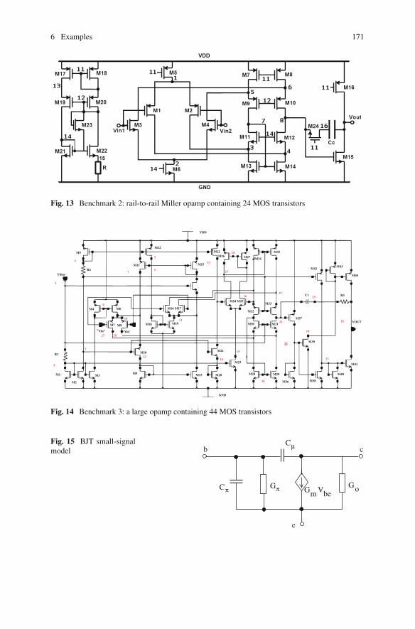
6 Examples 171
Fig. 13 Benchmark 2: rail-to-rail Miller opamp containing 24 MOS transistors
YDD
M5
R2M11
M12
M15
M22M26 M27 M34
M35
M33
M32
M25M24
M30 M31
M37
C1
M42M43
M44
R3
YOUT
M39
M41
M40
M38M36
M29M28M20
GND
M23
M21
M13
M19
M16 M17
M18
M10
M9
M2
M1
R1
M3
Yin-
M7 M8
M6M4
Ybias
22
24
21
23
25
26
1916
17
18
13
5
67
8
10
2827
9
3
4
1
2
12
11
14
15
20
22
Fig. 14 Benchmark 3: a large opamp containing 44 MOS transistors
Fig. 15 BJT small-signalmodel
beπC
e
Gπ
Cμ
Go
cb
Gm V

172 8 Hierarchical Analysis Methods
Table 1 Performance of the GPDD+DDD strategy
Ckt #T #Symb |G P DD| #Symb Mat. |DDD| Time (s) Mem.(GPDD) (DDD) size (MB)
#2 24 12 481 104 18 × 18 70,129 1.81 70#3 44 12 481 140 28 × 28 45,716 1.50 91
#T number of transistorsMat. size the MNA matrix dimension
significantly affect the runtime performance, see for example a discussion in [200].The design and usage of a hash table are fairly implementation dependent; the detailsare omitted.
Due to the above factors, the comparisons we made between different BDD-basedhierarchical implementations should be considered as factual report, not justifyingone implementation outperforms the other.
6.1 Examples for the GPDD+DDD Method
The experimental results by using the GPDD+DDD strategy are summarized inTable 1. We have tested this strategy only on the two CMOS opamp circuits withthe symbolic stamp for the MOSFET small-signal model constructed by GPDD. Thecolumn “#T” lists the number of MOS transistors in each benchmark. The column“#Symb (GPDD)” lists the total number of symbols involved in the symbolic stampfor the small-signal device model. The GPDD size for representing a MOSFETstamp is 481 vertices, which is listed in the column |G P DD|. The column “#Symb(DDD)” lists the number of symbols (i.e., nonzero entries) in the MNA matrix thatassembling all symbolic stamps, which is analyzed by DDD. We also list the MNAmatrix size in the column “Mat. Size” for reference. The number of DDD verticescreated for the MNA matrix is listed in the column |DDD|. The time listed in thecolumn “Time” is the total CPU time for completing the whole hierarchical analysis,including circuit parsing, BDD constructions, and producing one ac analysis over100 frequency points. We found that the GPDD and DDD construction time wasmuch less than the ac evaluation time, which had to traversal the data structure 100times for 100 frequency points. The column “Mem.” lists the memory consumptionfor running each benchmark.
The implementation was based on constructing one GPDD stamp for all MOSFETdevices, which is repeatedly invoked during evaluation. The 16-root GPDD (standingfor the 16 transadmittances) for the four-port MOSFET device were created with481 vertices by using a freely chosen symbol order. A smaller GPDD is possibleif we slightly optimize the symbol order for the symbolic stamp. The hierarchicalformulation resulted in a 18 × 18 MNA matrix for Benchmark 2 and a 28 × 28MNA matrix for Benchmark 3. We implemented a Greedy Order [196] for the DDDroutine proposed in [200]. It is interesting to mention that the DDD created for

6 Examples 173
Table 2 Two-level partition list for Benchmark 1 (μA725)
Id Components
L1,1 L2,1, L2,2, L2,3
L2,1 Q1, Q2, Q3, Q4, R1, R2, R3, R4
L2,2 Q5, Q10, R7, R10, Q6, Q16, R6, Q7, Q8, Q11,
Q12, R8, R17, Q9, Q17, R18, Q15, R5
L2,3 Q13, Q18, Q19, R11, Q21, Q23, Q26, R15, R16,
Q14, Q20, Q22, Q24, Q25, R12, R13, R14, R19
the Benchmark 2 has a larger size (70,129 vertices) than that for the Benchmark 3(45,716 vertices) although the latter circuit has a larger matrix dimension. This isjust an indication of the sensitivity of DDD performance to the symbol order. Thereis no definite correlation between the matrix size and the DDD size when differentsparsity and different symbol orders are involved [199].
The two benchmark circuits could not be solved by the non-hierarchical DDDand GPDD implementations we implemented due to memory overflow. Hence, theexperiment has demonstrated the effectiveness by a hierarchical strategy. We alsoobserve that the two-level hierarchical method is less sensitive to the number oftransistors in the circuit. The two benchmarks have largely different numbers ofdevices, but the total analysis times and memory usage do not differ drastically, asseen from Table 1.
6.2 Examples for the HierGPDD Method
In this section we compare the performance of the HierGPDD implementation to animplementation of using the Schur-decomposition-based hierarchical DDD [236],which is codenamed Schur-DDD for the purpose of comparison. The Schur-DDDmethod is based on the construction of symbolic DDD stamps for all circuit modules atdifferent levels. The algorithm in [200] was used in the Schur-DDD implementation.
The first benchmark μA725 opamp was also used in the experiment. This circuitwas considered hard to solve by using a non-hierarchical BDD-based method. Theoriginal implementation of DDD in [196] did not solve this circuit. However, μA725was once solved by the de-cancellation method in [231] and the GPDD in [204], bothnon-hierarchical.
We attempted two partitions for μA725, one in two levels listed in Table 2 and theother in three levels listed in Table 3. In the tables the module index Lm,n refers tothe nth module in the mth partition level (from top down). In this sense L1,1 refersto the top-level circuit (i.e., the main circuit).
The performances of the two programs, HierGPDD and Schur-DDD, were com-pared for the μA725 circuit with two different partitions. The first partition had twolevels and the result is shown in Table 4. The second partition had three levels and

174 8 Hierarchical Analysis Methods
Table 3 Three-level partition list for Benchmark 1 (μA725)
Id Components
L1,1 L2,1,L2,2,L2,3
L2,1 Q1,Q2,Q3,Q4,R1,R2,R3,R4
L2,2 L3,1,L3,2,L3,3,L3,4,Q15,R5
L2,3 L3,5,L3,6,L3,7
L3,1 Q5,Q10,R7,R10
L3,2 Q6,Q16,R6
L3,3 Q7,Q8,Q11,Q12,R8,R17
L3,4 Q9,Q17,R18
L3,5 Q13,Q18,Q19,R11
L3,6 Q21,Q23,Q26,R15,R16
L3,7 Q14,Q20,Q22,Q24,Q25,R12,R13,R14,R19
Table 4 Performance comparison for Benchmark 1 (μA725) with two levels
Id #E #N #P |G P DD| GPDD |DDD| DDDCPU time (s) CPU time (s)
L1,1 34 7 – 773 0.016 130 0.013L2,1 26 8 4 548 0.046 341 0.063L2,2 62 16 4 135,785 3.015 11,870 1.999L2,3 62 13 3 91,682 2.067 12,022 0.687Total – – – 228,788 5.165 24,363 2.781
#E number of edges; #N number of nodes; #P number of ports
the result is shown in Table 5. We observe that a finer partition resulted in fasteranalysis and less memory.
Next, Benchmark 2 (the two-stage rail-to-rail opamp) was partitioned as listed inTable 6. The test results were collected in Table 7. We observe that although a largerGPDD (total number of GPDD vertices) was constructed in this test, the runtime wasless.
Finally, we make an accumulated comparison for all three benchmark circuits.Benchmark 3 is a relatively large opamp circuit, which was also solved earlier byby the GPDD+DDD strategy. A five-level partition is listed in Table 8. The runtimeperformance on this circuit is listed together with the rest two in Table 9. We see thatboth HierGPDD and Schur-DDD could solve the three opamp circuits in less thanabout 10 s.
It is interesting to observe that the HierGPDD program sometimes constructed alarger hierarchical GPDD than the GPDD+DDD program did (becauseHierGPDD involves more symbols in general); however, the overall constructionspeed of HierGPDD was not necessarily slower.
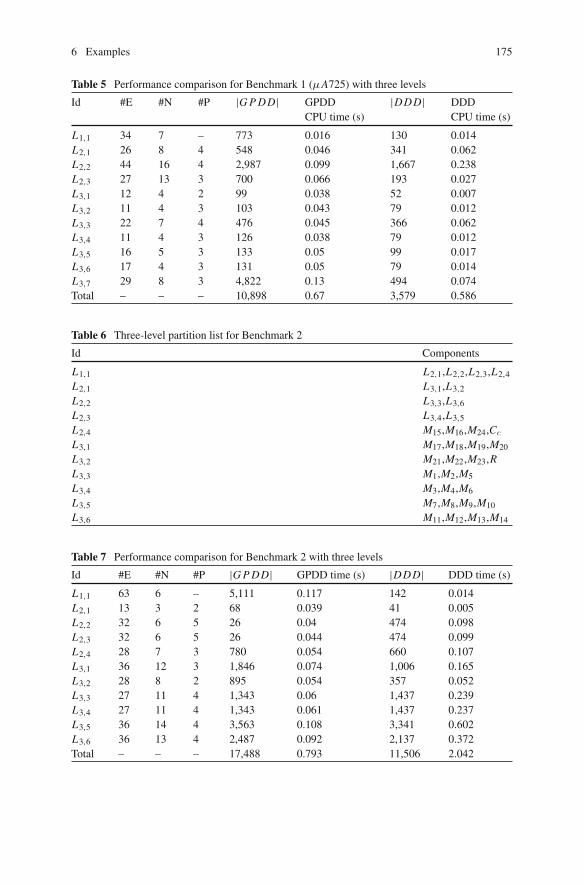
6 Examples 175
Table 5 Performance comparison for Benchmark 1 (μA725) with three levels
Id #E #N #P |G P DD| GPDD |DDD| DDDCPU time (s) CPU time (s)
L1,1 34 7 – 773 0.016 130 0.014L2,1 26 8 4 548 0.046 341 0.062L2,2 44 16 4 2,987 0.099 1,667 0.238L2,3 27 13 3 700 0.066 193 0.027L3,1 12 4 2 99 0.038 52 0.007L3,2 11 4 3 103 0.043 79 0.012L3,3 22 7 4 476 0.045 366 0.062L3,4 11 4 3 126 0.038 79 0.012L3,5 16 5 3 133 0.05 99 0.017L3,6 17 4 3 131 0.05 79 0.014L3,7 29 8 3 4,822 0.13 494 0.074Total – – – 10,898 0.67 3,579 0.586
Table 6 Three-level partition list for Benchmark 2
Id Components
L1,1 L2,1,L2,2,L2,3,L2,4
L2,1 L3,1,L3,2
L2,2 L3,3,L3,6
L2,3 L3,4,L3,5
L2,4 M15,M16,M24,Cc
L3,1 M17,M18,M19,M20
L3,2 M21,M22,M23,RL3,3 M1,M2,M5
L3,4 M3,M4,M6
L3,5 M7,M8,M9,M10
L3,6 M11,M12,M13,M14
Table 7 Performance comparison for Benchmark 2 with three levels
Id #E #N #P |G P DD| GPDD time (s) |DDD| DDD time (s)
L1,1 63 6 – 5,111 0.117 142 0.014L2,1 13 3 2 68 0.039 41 0.005L2,2 32 6 5 26 0.04 474 0.098L2,3 32 6 5 26 0.044 474 0.099L2,4 28 7 3 780 0.054 660 0.107L3,1 36 12 3 1,846 0.074 1,006 0.165L3,2 28 8 2 895 0.054 357 0.052L3,3 27 11 4 1,343 0.06 1,437 0.239L3,4 27 11 4 1,343 0.061 1,437 0.237L3,5 36 14 4 3,563 0.108 3,341 0.602L3,6 36 13 4 2,487 0.092 2,137 0.372Total – – – 17,488 0.793 11,506 2.042

176 8 Hierarchical Analysis Methods
Table 8 Five-level partition list for Benchmark 3
Id Components
L1,1 L2,1, L2,2
L2,1 L3,1, L3,2
L2,2 R3, C1, L3,3, L3,4, M36, M37
L3,1 L4,1, M32, M33
L3,2 L4,2, L4,3, M30, M31
L3,3 M39, M43, M44
L3,4 M38, M40, M41, M42
L4,1 L5,1, L5,2, L5,3, L5,4, L5,5
L4,2 M28, M29
L4,3 L5,6, L5,7, L5,8
L5,1 R2, M5, M12, M22
L5,2 M16, M17, M18, M19
L5,3 R1, M1, M2, M3, M23
L5,4 M20, M21
L5,5 M24, M25, M26, M27, M34, M35
L5,6 M11, M14, M15
L5,7 M4, M6, M7, M8
L5,8 M9, M10, M13
Table 9 Performance comparison for the three benchmarks
Ckt L #E #N |G P DD| GPDD time (s) |DDD| DDD time (s)
#1 3 166 31 10,432 0.682 3,579 0.586#2 3 218 66 17,488 0.793 11,506 2.042#3 5 399 114 197,274 6.771 62,794 10.359
L number of partition levels; #E number of edges;#N number of nodes
7 Summary
In this chapter we have presented several BDD-based hierarchical symbolic analysisstrategies by emphasizing the technique of symbolic stamp. A contribution to thegraphical analysis of multiport modules is also presented, which makes GPDD amore powerful method for analyzing large analog circuit by multilevel partition. Wehave recommended the use of GPDD symbolic stamps for the bottom-level circuitmodules that have identical topologies. Data sharing is the most important propertythat makes the BDD-based hierarchical construction profitable.
Among many possibilities of hierarchical constructions, we have mainlyinvestigated two strategies, GPDD+DDD and HierGPDD, for which experimentalcomparisons have been made. It has been demonstrated that both hierarchical strate-gies could efficiently solve large analog circuits in a matter of seconds. A majorconclusion we may draw is that circuit partitioning weakens the strict dependenceof a BDD method on symbol ordering for large circuits, meanwhile significantly

7 Summary 177
Table 10 Capacity comparison of the published hierarchical methods
Work Ref. size (#T) Method Accuracy
[236] 20/BJT Schur + DDD Exact[39] 26/BJT Regularity + Sharing Exact[70] 83/MOS Ckt Reduction + Two-graph Approx.[231] 26/BJT DDD + De-cancellation ExactBDD-based 44/MOS DDD + GPDD Exact
#T number of transistors
reduces the BDD construction complexity. It seems that with hierarchical analysis,there is no obstacle to symbolic analysis of large-scale analog integrated circuits.
This chapter is ended by a comparison of the capacities of several published hier-archical analysis methods. We list in Table 10 the reference circuit sizes (Ref. size)(representing the maximum sizes reported in the cited publications), the methodemployed, and whether or not approximation is involved. Except for the work[70] which promoted approximate hierarchical analysis, the BDD-based hierarchicalexact analysis methods addressed in this chapter was capable of solving the largestcircuit.
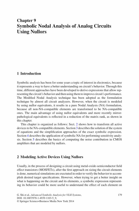
Chapter 9Symbolic Nodal Analysis of Analog CircuitsUsing Nullors
1 Introduction
Symbolic analysis has been for some years a topic of interest in electronics, becauseit represents a way to have a better understanding on circuit’s behavior. Through thistime, different approaches have been developed to derive expressions that allow rep-resenting the circuit’s behavior and then using them to improve circuit’s performance.The Modified Nodal Analysis technique has been adopted as the formulationtechnique by almost all circuit analyzers. However, when the circuit is modeledby using nullor equivalents, it results in a pure Nodal Analysis (NA) formulation,because all non-NA-compatible elements are transformed to be NA-compatibleones. The main advantage of using nullor equivalents and more recently mirror-pathological equivalents is reflected in a reduction of the matrix rank, as shown inthis chapter.
This chapter is organized as follows: Sect. 2 shows how to transform all activedevices to be NA-compatible elements. Section 3 describes the solution of the systemof equations and the simplification approaches of the exact symbolic expression.Section 4 describes the application of symbolic NA for performing sensitivity analy-sis. Section 5 describes the basics of computing the noise contribution in CMOSamplifiers that are modeled by nullors.
2 Modeling Active Devices Using Nullors
Usually, in the process of designing a circuit using metal-oxide-semiconductor fieldeffect transistors (MOSFETs), after the first approach on sizing the circuit elementsis done, numerical simulations are exectuted in order to verify the behavior to accom-plish desired target specifications. However, when trying to get a better insight onwhat is happening on the circuit and its elements, a symbolic expression represent-ing its behavior could be more useful to understand the effect of each element on
G. Shi et al., Advanced Symbolic Analysis for VLSI Systems, 179DOI: 10.1007/978-1-4939-1103-5_9,© Springer Science+Business Media New York 2014

180 9 Symbolic Nodal Analysis of Analog Circuits Using Nullors
Fig. 1 Nullor description as atwo-port network
the circuit’s performances. That way, symbolic analysis play an important role toimprove circuit design, as shown by the works introduced in [44, 45, 240, 241].
Symbolic analysis approaches can be enhanced by improving three main stages:formulation of the circuit equations, solution and simplification or reduction of thesymbolic expressions. The first stage can be improved by deriving models thatshould be different from traditional ones based on controlled sources, and whichshould reduce the rank of the admittance matrix compared to traditional ModifiedNodal Analysis (MNA). In this manner, this chapter shows that by using nullors, andrecently mirror-pathological elements [178], all active devices can be transformedto be NA-compatible ones, to formulate a reduced number of equations compared totraditional MNA formulation, as already shown in [180].
Using nullors and mirror-pathological elements to model the behavior of activedevices in an analog circuit, leads us to perform pure nodal analysis (NA), where onlyadmittances and current sources can be dealt with. The NA formulation is describedby (1), where Yn is the admittance matrix, vn is the variables vector, and in is thestimulus or solution vector including intependent current sources.
Ynvn = in (1)
2.1 Nullor Concept
In 1954 Tellegen showed that an ideal amplifier could be used as a general blockfor implementing linear or non-linear circuits. In 1964, Carlin proposed the Nullorfor modeling the behavior of the ideal amplifier as a two ports element with fourassociated variables, as shown by Fig. 1. As one sees, the nullor is composed by anullator located at its input-port and a norator at the output-port.
The properties of the nullor are: the nullator has the property that both variablesVo and Io are always zero. Conversely, the norator has the property that its voltageVp and current Ip are arbitrarily assigned. These properties have been exploited tosynthesize analog integrated circuits [41], and to propose different kinds of modelsfor modern active devices, as already shown in [85, 117, 119, 148, 188, 181, 212,226, 243, 244]
In this chapter the nullor properties are exploited to obtain compacted systemsof equations for analog integrated circuits (ICs). That way, by applying the nullator

2 Modeling Active Devices Using Nullors 181
Fig. 2 Nullator and norator connections in a nullor network
and norator properties, the NA formulation for an analog IC modeled by nullors isperformed as follows:
1. If a nullator is grounded, as shown in Fig. 2a, from its voltage property, nodei should be grounded and therefore eliminated as voltage variable, i.e. it reducesone column in Yn .
2. If a nullator is floating, as shown in Fig. 2b, from its voltage property, nodesi and j are virtually connected, so that both are associated to a single voltagevariable, thus reducing one column in Yn .
3. If a norator is grounded, as shown in Fig. 2c, from its current property, nodei should be grounded and therefore eliminated as current variable, i.e. it reducesone row in Yn .
4. If a norator is floating, as shown in Fig. 2d, from its current property, nodes i andj are virtually connected, so that both are associated to a single current variable,thus reducing one row in Yn .
2.2 Nullor Equivalent of the MOSFET
To take advantage on performing computer-aided analysis, active devices should bemodeled to improve circuit analysis. In IC design, the most used active device is theMOSFET, for which the nullor equivalent that models its most abstract small-signalbehavior is shown in Fig. 3. In this case, the nullator property forces the voltage atterminal G to be processed by the transconductance gm , thus generating a currenti = gmvGS . From the norator property, the current through the norator is the onethrough gm , therefore: iDS = gmvGS .
As one can infer, this description of the MOSFET using the nullor and oneconductance is equivalent to the voltage-controlled current source (VCCS), whichnullor equivalent is shown in Fig. 4. One can note in that Figure that the nullor equiv-alents of the other controlled sources are based on this VCCS. The usefulness of thistransactors is highlighted in the follwing sections when performing symbolic NA ofanalog ICs.

182 9 Symbolic Nodal Analysis of Analog Circuits Using Nullors
Fig. 3 Small-signal model of the three terminals MOSFET using the nullor
Fig. 4 Nullor equivalents of the four controlled sources
Figure 5 shows the four terminals MOSFET including some parasitics, and usingtwo VCCSs. Further, the nullor equivalent consists of replacing the VCCSs by thenullor equivalent from Fig. 4. However, in this case the nullor in the bottom terminalsis replaced by a short-circuit, as already shown in [45, 241], leading to use the nullorequivalent shown in Fig. 3. At the end, the nullor equivalent of the four terminalsMOSFET is shown in Fig. 6, for which other parasitics can be added among itsrespective terminals.

2 Modeling Active Devices Using Nullors 183
Fig. 5 Small-signal model of the four terminals MOSFET using controlled sources
Fig. 6 Small-signal model of the four terminals MOSFET using the nullor and includingparasitics
2.3 Nullor Equivalents of Active Devices
The transactors shown in Fig. 4 have been traditionally used to model the abstractbehavior of all kinds of active devices. However, nowadays the voltage mirror andcurrent mirror pathological elements have demonstrated their usefulness in derivingmore compact models of the active devices, as already shown in [178, 180, 243].Those pathological elements combined with nullors made possible the generation ofcompacted models for modern active devices, which are listed in [188].
For instance, the operational transresistance amplifier (OTRA) [181], can bedirectly modeled using the nullor equivalent of the current-controlled voltage source(CCVS) shown in Fig. 4. However, some manipulations among nullators and noratorsleads us to derive compacted models. As an example, the current-feedback opera-tional amplifier (CFOA) is basically composed of one current mirror sandwiched bytwo voltage followers, as already shown in [241]. Using the nullor equivalents from

184 9 Symbolic Nodal Analysis of Analog Circuits Using Nullors
Fig. 7 Nullor equivalent of the current-feedback operational amplifier
Fig. 4, one can use the current-controlled current source (CCCS) to implement thecurrent mirror, or one can use a pathological current mirror, and to implement thevoltage followers, one can use the nullor equivalent of the voltage-controlled voltagesource (VCVS) shown in Fig. 4. It is clear that the nullor equivalent of the CFOAwill have many elements. Figure 7 shows a compacted model for the CFOA, whichwas obtained by manipulations among the nullators and norators in the CCCS andthe two VCVSs. The CFOA is commercially available from analog devices with thename AD844.
In a similar way, other nullor equivalents for other active devices can be derivedby combining the transactors from Fig. 4, and by exploiting the properties of thenullor. Other quite useful active devices for analog signal processing applicationsare the current conveyors, which are summarized in [244] using nullors, and somenullor equivalents for the first-generation, second-generation and third-generation areshown in Figs. 8, 9 and 10, respectively. Those nullor equivalents can be compactedby using the mirror pathological elements as shown in [178, 188]. Besides, the nullorequivalents are used herein to perform symbolic NA of active filters in the followingsubsections.
2.4 Nullor Equivalents of CMOS Amplifiers
As mentioned above, one can manipulate the nullors exploting its nullator-noratorproperties, so that one can obtain compacted models. In the analysis of CMOS ampli-fiers, the MOSFET shown in Fig. 6 can be compacted to the one shown in Fig. 11.Further, using this model in a CMOS operational amplifier, as in the uncompensatedthree-stages one, the nullor equivalent is shown in Fig. 12.
This equivalent can also be reduced by applying the nullator-norator proper-ties, and also it can be reduced by using mirror pathological elements, as shownin [178, 188]. In the following section it is shown how formulating the nodal admit-tance matrix for analog ICs modeled by nullor circuits.

2 Modeling Active Devices Using Nullors 185
Fig. 8 Nullor equivalents of four descriptions for the first-generation current conveyor
Fig. 9 Nullor equivalents of four descriptions for the second-generation current conveyor
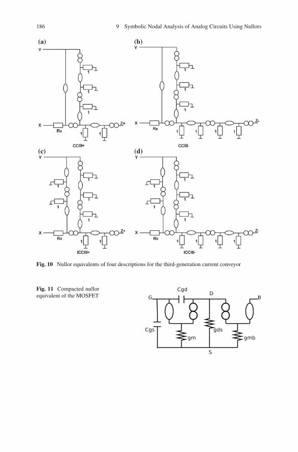
186 9 Symbolic Nodal Analysis of Analog Circuits Using Nullors
Fig. 10 Nullor equivalents of four descriptions for the third-generation current conveyor
Fig. 11 Compacted nullorequivalent of the MOSFET

3 Deriving Symbolic Expressions and Simplification Approaches 187
Fig. 12 Nullor equivalent of a three stages operational amplifier
3 Deriving Symbolic Expressions and SimplificationApproaches
The guidelines for formulating the nodal admittance matrix by performing symbolicNA of nullor circuits is well described in [180], and in Chap. 5 in [44], and it issummarized herein as follows:
1. Replace all active devices and non-NA compatible elements (e.g. independentvoltage sources), by their nullor-equivalents.
2. Describe the interconnection relationships of norators Pj , nullators O j , andadmittances by generating tables including names and nodes (m, n).
3. Calculate the indexes associated to set row (ROW) and set column (COL), andgroup grounded and floating admittances:
(a) ROW: Contains all nodes ordered by applying the norator property, wherenodes (m, n) are virtually short-circuited. These indexes are used to fillvector i and the admittance matrix Y .
(b) COL: Contains all nodes ordered by applying the nullator property, wherenodes (m, n) are virtually short-circuited. These indexes are used to fillvector v and the admittance matrix Y .
(c) Admittances: They are grouped into tables A and B. Table A includes allnodes (ordered), and in each node is the sum of all admittances connectedto it. Table B includes all floating admittances and its nodes (m, n).
4. Use sets ROW and COL to fill vectors i and v, respectively, in the NA formulationdescribed by (1). To fill the admittance matrix Y : if in Table A a node is included inROW and COL, that admittance(s) is(are) inserted in Y at position (ROW index,COL index). For each admittance in Table B, search node m in ROW and n inCOL (do the same but search n in ROW and m in COL), if both nodes exist theadmittance is inserted in Y at position (ROW index, COL index), and is negative.

188 9 Symbolic Nodal Analysis of Analog Circuits Using Nullors
Table 1 Elements tables
Table type Fields
Conductances Name, node 1, node 2, valueIndependent sources Name, node 1, node 2, DC, ACControlled sources Name, node 1, node 2, node 3, node 4, gainMOSFET Name, drain, gate, source, bulk, width, length, modelname
Fig. 13 Non-inverting CMOSlow voltage amplifier
M1 M2
M4M3
Vin Vref
Vout
The formulation of the nodal admittance matrix by computer-aided analysis parsesthe netlist, e.g. from HSPICE, and builds suitable data structures for each group ofcircuit elements, as described above for Tables A and B. The symbolic name givento each circuit element in the nullor equivalent for a MOSFET, is tracked to the oneassociated to its name. In this manner, to keep consistency, the symbol name is takenexactly as specified in the netlist (example: R_name, C_name, M_name, etc.). Thatway, the circuit elements are grouped into one of the four Tables for: conductances,independent sources, controlled sources and MOSFETs, as shown in Table 1.
The formulation approach is applied to the non-inverting CMOS low voltageamplifier shown in Fig. 13. Its nullor-equivalent is shown in Fig. 14. Using thenullor-equivalent in Fig. 15, the simple CMOS current mirror formed by M3-M4,is described among nodes 4, 5, 6 and 8 with gain Ai and output conductance go4.The input resistance and parasitic capacitors are not taken into account because thebandwidth of the CMOS current mirrors, is higher than that of the blocks processingvoltage signals.
The sets ROW = {(1),(3,4,5),(6,7,8)} and COL = {(1,2,3), (5,6),(8)}, generates(2), whose solution is given by (3). The current gain of the current mirror is given asAi = gm4/gm3.
⎡vin
00
⎢
⎣ =
⎡1 0 0
gm1 1 00 Ai go2 + go4
⎢
⎣
⎡v1,2,3v5,6v8
⎢
⎣ (2)
vout
vin= gm1 Ai
go2 + go4(3)

3 Deriving Symbolic Expressions and Simplification Approaches 189
Fig. 14 Nullor-equivalent of Fig. 13
Fig. 15 Nullor-equivalent of the current mirror including input impedance, independent gain andoutput impedance at each output (n)
3.1 Symbolic Analysis Using Nullor-Equivalents ofCurrent-Mirrors
This subsection shows the usefulness of using nullor-equivalents of current mirrors togenerate the symbolic behavioral model of CMOS amplifiers. Basically, the currentmirrors are replaced by their nullor-equivalents which include performances para-meters like gain, input and output impedances. The nullor-equivalent can providemultiple outputs, but each path with independent output impedance and current gainrelationship.

190 9 Symbolic Nodal Analysis of Analog Circuits Using Nullors
Fig. 16 Cascode current mirror and its nullor-based description
For instance, in the majority of cases CMOS current mirrors provide widerbandwidth than blocks driving voltage signals. This property allows us to discrimi-nate parasitic capacitors in CMOS current mirrors, so that a proposed generic nullor-equivalent includes only the current gain and output conductances, as shown inFig. 15. That way, using this nullor equivalent in performing symbolic NA leadsus to generate a much small and sparse matrix than by using traditional controlledsources.
The usefulness of using nullors and pathological elements to calculate simplifiedsymbolic behavioral models of analog ICs has been already demonstrated in [44, 45,178, 180, 240, 241] and highlighted that the main advantage is the order reductionof the admittance matrix compared to traditional formulation methods, and whenmodeling the active devices using controlled sources. This subsection shows theusefulness of using a generic nullor-equivalent for the current mirror, so that notonly one can reduce the order of the matrix, but also one can use the same symbolicbehavioral expression for any kind of current mirror and including its non-idealcharacteristics, e.g. admittances and gain.
The generic nullor-equivalent of the current mirror is shown in Fig. 15, where byconsidering the directions of the currents, the output ones ioutn , are negative. First,this subsection shows how to calculate the current gain and output resistance (Ai
and Rout ) of the simple and cascode current mirrors. The current gain Ai is furtherassociated to the ratio among the widths and lengths of the MOSFETs to perform abetter sizing approach in a post-processing step.
From the simple current mirror shown in Fig. 13, Ai in (3) equals to gm4/gm3, androut = 1/go4, as shown in Fig. 14. By applying this to the dual-output current mirrorCM-N shown in Fig. 17, one derives two gains Ai1 = gm6/gm5 with ro1 = 1/go6,and Ai2 = gm7/gm5 with ro2 = 1/go7.
Now, for the cascode current mirror shown in Fig. 16b, by applying symbolic NA,the sets ROW = (1,5),(2,6),(3,7),(4,8) and COL = (1,5,6),(2),(3,7,8),(4). The systemformulation is given by (4). The solution for Ai = gm2/gm1 with M4 = M2 and

3 Deriving Symbolic Expressions and Simplification Approaches 191
Fig. 17 CMOS Miller amplifier
M3 = M1. Performing symbolic NA with the addition of the output conductances toM2 and M4 leads us to derive ro = gm4/(go4go2).
⎤⎤⎡
iin
000
⎢
⎥⎥⎣ =
⎤⎤⎡
gm3 0 −gm3 0gm4 gL 0 −gm4
−gm3 0 gm1 + gm3 0−gm4 0 gm2 gm4
⎢
⎥⎥⎣
⎤⎤⎡
v1,5,6v2
v3,7,8v4
⎢
⎥⎥⎣ (4)
3.2 Symbolic Behavioral Modeling for CMOS amplifiers
In another example, the generation of the symbolic behavioral model for the CMOSMiller amplifier shown in Fig. 17, is described herein. The nullor-equivalent usingcurrent mirrors is shown in Fig. 18.
The symbolic NA formulation is given by the following description,
i =
⎤⎤⎤⎤⎤⎤⎡
vinn
vinp
0000
⎢
⎥⎥⎥⎥⎥⎥⎣
v =
⎤⎤⎤⎤⎤⎤⎡
v1,2,6v3,4,7v5
v9,10v11,12v13
⎢
⎥⎥⎥⎥⎥⎥⎣
(5)
Y =
⎤⎤⎤⎤⎤⎤⎡
1 0 0 0 0 00 1 0 0 0 0a b c 0 0 0d 0 −d 1 0 00 e −e f g h0 0 0 0 i j
⎢
⎥⎥⎥⎥⎥⎥⎣
(6)

192 9 Symbolic Nodal Analysis of Analog Circuits Using Nullors
Fig. 18 Nullor-equivalent of the CMOS Miller amplifier
where
a = −sCgs1 − gm1
b = −gm2 − sCgm2
c = gm1 + gm2 + go6 + s(Cgs1 + Cgs2)
d = gm1
e = gm2
f = Aip
g = go4 + sCm
h = −sCm
i = −sCm + gm8
j = sCm + go7 + go8
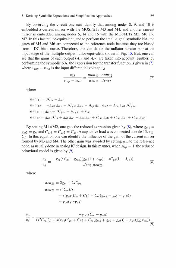
3 Deriving Symbolic Expressions and Simplification Approaches 193
By observing the circuit one can identify that among nodes 8, 9, and 10 isembedded a current mirror with the MOSFETs M3 and M4, and another currentmirror is embedded among nodes 5, 14 and 15 with the MOSFETs M5, M6 andM7. In this last nullor-equivalent, and to perform the small-signal symbolic NA, thegates of M5 and M6 are connected to the reference node because they are biasedfrom a DC bias source. Therefore, one can delete the nullator-norator pair at theinput stage of the multiple-output nullor-equivalent shown in Fig. 15. But, one cansee that the gains of each output (Ai1 and Ai2) are taken into account. Further, byperforming the symbolic NA, the expression for the transfer function is given in (7),where vinp − vinn is the input differential voltage vd .
v13
vinp − vinn= num11 · num12
den11 · den12(7)
where
num11 = sCm − gm8
num12 = −gm1 gm2 − sCgs1 gm2 − Aip gm1 gm2 − Aip gm1 sCgs2
den11 = gm2 + sCgs2 + sCgs1 + gm1
den12 = go4 sCm + go4 go8 + go4 go7 + sCm go8 + sCm go7 + sCm gm8
By setting M1 = M2, one gets the reduced expression given by (8), where gm1 =gm2 = gm and Cgs1 = Cgs2 = Cgs . A capacitive load was connected at node 13, e.g.CL . In this equation one can identify the influence of the gain of the current mirrorformed by M3 and M4. The other gain was avoided by setting go6 to the referencenode, as usually done in analog IC design. In this manner, when Aip = 1, the reducedbehavioral model is given by (9).
vo
vd= −gm(sCm − gm8)(gm(1 + Aip) + sCgs(1 + Aip))
den21den22(8)
where
den21 = 2gm + 2sCgs
den22 = s2CmCL
+ s(go4(Cm + CL) + Cm(gm8 + go7 + go8))
+ go4(go7go8)
vo
vd= −gm(sCm − gm8)
(s2CmCL + s(go4(Cm + CL) + Cm(gm8 + go7 + go8)) + go4(go7go8))(9)
194 9 Symbolic Nodal Analysis of Analog Circuits Using Nullors
Fig. 19 Graph representation of (10)
3.3 Solving the Symbolic NA Formulation for Large Circuits
The circuit size is a challenge in performing symbolic NA because a large number ofsymbolic terms are manipulated [45, 240, 241]. Fortunately, this problem is mitigatedwhen applying DDDs, and variants of it as the graph-based symbolic technique(GBST) introduced in [44], which has a special representation of the admittancematrix as shown in this subsection.
The GBST has a unique and compact representation for a large class of analogICs, so that every determinant has a unique representation and is liable to symbolicmanipulations. Lets us consider the following determinant:
det (M) =
⎦⎦⎦⎦⎦⎦⎦⎦
a b 0 0c d e 00 f g h0 0 i j
⎦⎦⎦⎦⎦⎦⎦⎦
= adg j − adhi − ae f j − bcg j + bchi (10)
The GBST generates a graph from a determinant’s size n×n. The generated graphhave paths of n + 1 levels, and it is build in a depth-first search (DFS) fashion. Eachelement in the graph structure corresponds to an element in the admittance matrix.In this manner, the first step for generating the graph for (10) is shown in Fig. 19. Asone sees, several nodes are shared, so that the final graph is shown in Fig. 20. Theprocedure is well described in [44].
For instance, the implementation of this graph structure is by a tree in which thearithmetic operations are encoded in the depth of the tree node, that is, different depthimplies multiplication while equal depth implies addition. This leads us to get thesimplified symbolic expression for (10):
det (M) = a [d (g j − hi) + e (− f j)] + b [c (−g j + hi)] (11)

3 Deriving Symbolic Expressions and Simplification Approaches 195
Fig. 20 Graph equivalentfrom Fig. 19 with node re-use
By applying the GBST, not only one can obtain a factorized exact symbolicexpression, but also one can derive all transfer relationships for large circuits withrespect to each node, and in a post-processing step to each branch circuit variable.In addition, the GBST approach is suitable to directly perform sensitivity analysis,as shown in the next section.
3.4 Small-Signal Models and Nullor Equivalentsby Levels of Abstraction
It is evident that the more complex the small-signal model of an active device themore accurate is the resulting simulation but at the cost of increasing computingrequirements and time. A trade-off can be identified for generating nullor equivalentsat different levels of abstraction. In the GBST introduced in [44], three levels ofabstraction were presented, each one including different parasitic elements for theMOSFET, they are:
• Level 0 has no parasitic elements and models only the voltage-controlled currentsource (VCCS) with gate-source as the controlling branch voltage and transcon-ductance gm .
• Level 1 accounts for level 0 plus adding the parasitics Cgs , Cgd and gds .• Level 2 accounts for level 1 plus the voltage-controlled current source whose
controlling branch voltage is for modeling the bulk-source with transconductancegmb.
In most cases, the basic analog building blocks are composed of the voltage- andcurrent-followers, which nullor equivalents are shown in Fig. 21a and b, respectively.

196 9 Symbolic Nodal Analysis of Analog Circuits Using Nullors
Fig. 21 a Voltage follower. b Current follower ideal nullor equivalents without parasitics
When adding parasitics automatically, they are added to their corresponding struc-ture (conductance, independent source, nullator or norator), where their names areassociated to the name of the active device. For example, if we are including Cgs toa MOSFET named M1, the name of the new capacitor can be Cgs1. In this way, itbecomes easier to know to which netlist element a given symbol belongs.
4 Symbolic Sensitivity Analysis
The frequency response of a linear circuit is described by a transfer function thatcan be further used to perform a sensitivity analysis. That way, one can indentifythe circuit elements that may change and then modifying the response of the wholecircuit. In other words, the sensitivity is a measure of the variation of a circuit as awhole, due to the variation of a parameter or circuit element.
In general, the majority of sensitivity analysis techniques needs as input the trans-fer function H(s) that can be obtained by performing linear algebraic or graphoperations in a circuit. Herein the GBST is used to derive H(s) from nullor circuits.Again the OTA is used to derive three symbolic expressions: differential gain (Ad ),common-mode gain (Acm) and common-mode rejection ratio (CMRR). A sensitivityanalysis of these three expressions is symbolically realized to identify the most sen-sitive circuit elements. The derived analytical expressions for Ad , Acm and CMRRare numerically evaluated from HSpice simulations, and then the sensitivities areordered to rank from the most sensitive to the less sensitive one. At the end, theeffect of the sensitivities on the performances of an OTA is shown by simulating anominal design and selecting the most sensitive circuit parameters, which are variedin a certain percentage. The simulations are executed by using IC technology of0.5µm.
The OTA is shown in Fig. 22. Vb is a voltage to properly bias M6 and M7.Replacing each MOSFET by its nullor equivalent, the admittance matrix is for-
mulated as follows:
• Admittance matrix formulation

4 Symbolic Sensitivity Analysis 197
Fig. 22 Miller OTA
⎛
a −gds1 −gds2 0−gds1 − gm1 b −cgd4 ∗ s 0−gds2 − gm2 −cgd4 ∗ s + gm4 c −ycc − cgd5 ∗ s
0 0 −ycc + gm5 − cgd5 ∗ s d
⎧
⎪⎪⎨
where
a = gds7 + cgs1 ∗ s + gds1 + gds2 + cgs2 ∗ s + gm1 + gm2
b = gds1 + gm3 + gds3 + cgd1 ∗ s + cgs3 ∗ s + cgd4 ∗ s + cgs4 ∗ s
c = gds2 + gds4 + ycc + cgd5 ∗ s + cgd4 ∗ s + cgs5 ∗ s + cgd2 ∗ s
d = gds6 + gds5 + CL + ycc + cgd5 ∗ s
• Variables vector:
⎛
Vs
Vx
Vo1Vo
⎧
⎪⎪⎨
• Sources vector:
⎛
(gm1 + s ∗ cgs1) ∗ V1 + (gm2 + s ∗ cgs2) ∗ V2(−gm1 + cgd1 ∗ s) ∗ V1(−gm2 + cgd2 ∗ s) ∗ V2
0
⎧
⎪⎪⎨
Cl is the load capacitance and ycc is an equivalent admittance composed by theconductance gz and the capacitance Cc, it means:
ycc = gz ∗ Cc ∗ s
gz + Cc ∗ s(12)
The variables vector is formed by the nodal voltages Vs , Vx , Vo1 and Vo1, where Vs
denotes the node between transistors M7, M1 and M2; Vx denotes the node betweenM1, M3 and M4; Vo1 is the voltage at the output of the first stage and Vo refers
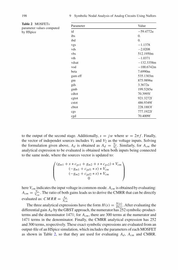
198 9 Symbolic Nodal Analysis of Analog Circuits Using Nullors
Table 2 MOSFETsparameter values computedby HSpice
Parameter Value
id −59.4772uibs 0.ibd 0.vgs −1.1378vds −2.0208vbs 512.1950mvth −1.0371vdsat −132.3358mvod −100.6742mbeta 7.6990mgam eff 535.1303mgm 875.9896ugds 3.3672ugmb 199.5285ucdtot 70.3995fcgtot 921.3272fcstot 486.9349fcbtot 228.1883fcgs 777.1922fcgd 70.4009f
to the output of the second stage. Additionally, s = jw where w = 2π f . Finally,the vector of independet sources includes V1 and V2 as the voltage inputs. Solvingthe formulation given above, Ad is obtained as Ad = Vo
V2. Similarly, for Acm the
analytical expression to be evaluated is obtained when both inputs being connectedto the same node, where the sources vector is updated to:
⎛
(gm1 + s ∗ cgs1 + gm2 + s ∗ cgs2) ∗ Vcm
(−gm1 + cgd1 ∗ s) ∗ Vcm
(−gm2 + cgd2 ∗ s) ∗ Vcm
0
⎧
⎪⎪⎨
here Vcm indicates the input voltage in common-mode. Acm is obtained by evaluating:Acm = Vo
Vcm. The ratio of both gains leads us to derive the CMRR that can be directly
evaluated as: C M R R = AdAcm
The three analytical expressions have the form H(s) = N (s)D(s) . After evaluating the
differential gain Ad by the GBST approach, the numerator has 252 symbolic-product-terms and the denominator 1471; for Acm , there are 300 terms at the numerator and1471 terms in the denominator. Finally, the CMRR analytical expression has 252and 300 terms, respectively. These exact symbolic expressions are evaluated from anoutput-file of an HSpice simulation, which includes the parameters of each MOSFETas shown in Table 2, so that they are used for evaluating Ad , Acm and CMRR.

4 Symbolic Sensitivity Analysis 199
Fig. 23 Simulated versus calculated differential gain comparison
Fig. 24 Simulated versus calculated common-mode gain comparison
A numerical comparison is shown in Figs. 23, 24 and 25. The errors appear becauseseveral parasitic components were neglected, as discussed above.
Further, the sensitivity can be calculated from the transfer functions H(s) =N (s)/D(s), as follows:
Sens(H(s), W ) = W
H(s)
∂ H(s)
∂(W )(13)
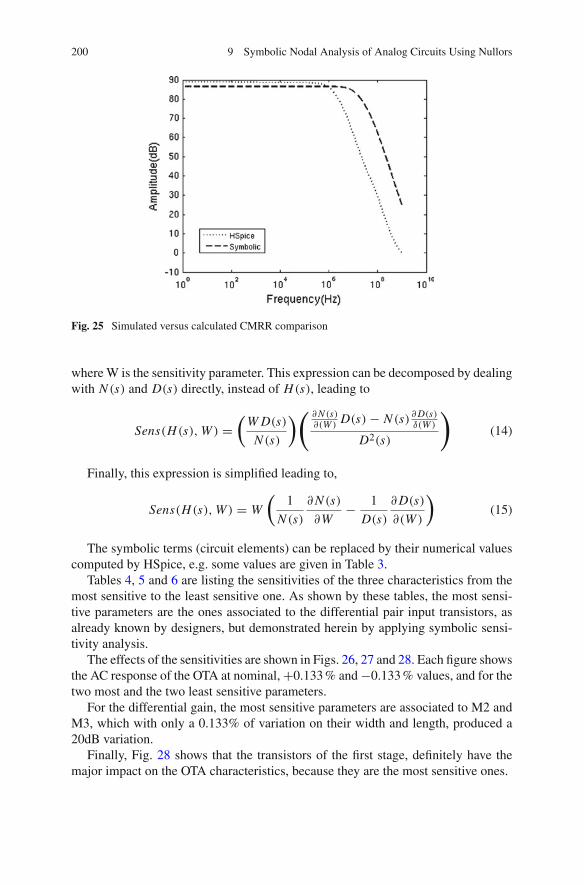
200 9 Symbolic Nodal Analysis of Analog Circuits Using Nullors
Fig. 25 Simulated versus calculated CMRR comparison
where W is the sensitivity parameter. This expression can be decomposed by dealingwith N (s) and D(s) directly, instead of H(s), leading to
Sens(H(s), W ) =⎩
W D(s)
N (s)
⎠(∂ N (s)∂(W )
D(s) − N (s) ∂ D(s)δ(W )
D2(s)
)
(14)
Finally, this expression is simplified leading to,
Sens(H(s), W ) = W
⎩1
N (s)
∂ N (s)
∂W− 1
D(s)
∂ D(s)
∂(W )
⎠
(15)
The symbolic terms (circuit elements) can be replaced by their numerical valuescomputed by HSpice, e.g. some values are given in Table 3.
Tables 4, 5 and 6 are listing the sensitivities of the three characteristics from themost sensitive to the least sensitive one. As shown by these tables, the most sensi-tive parameters are the ones associated to the differential pair input transistors, asalready known by designers, but demonstrated herein by applying symbolic sensi-tivity analysis.
The effects of the sensitivities are shown in Figs. 26, 27 and 28. Each figure showsthe AC response of the OTA at nominal, +0.133 % and −0.133 % values, and for thetwo most and the two least sensitive parameters.
For the differential gain, the most sensitive parameters are associated to M2 andM3, which with only a 0.133% of variation on their width and length, produced a20dB variation.
Finally, Fig. 28 shows that the transistors of the first stage, definitely have themajor impact on the OTA characteristics, because they are the most sensitive ones.
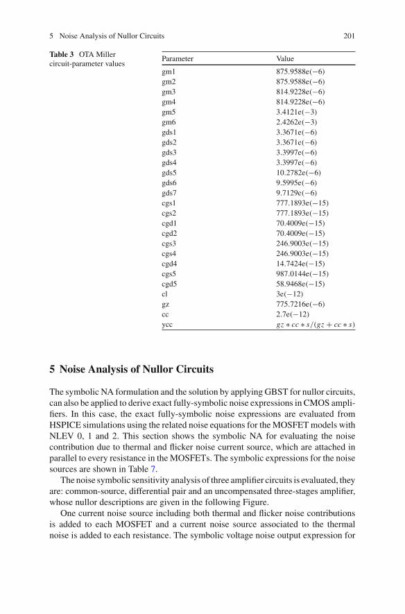
5 Noise Analysis of Nullor Circuits 201
Table 3 OTA Millercircuit-parameter values
Parameter Value
gm1 875.9588e(−6)
gm2 875.9588e(−6)
gm3 814.9228e(−6)
gm4 814.9228e(−6)
gm5 3.4121e(−3)
gm6 2.4262e(−3)
gds1 3.3671e(−6)
gds2 3.3671e(−6)
gds3 3.3997e(−6)
gds4 3.3997e(−6)
gds5 10.2782e(−6)
gds6 9.5995e(−6)
gds7 9.7129e(−6)
cgs1 777.1893e(−15)
cgs2 777.1893e(−15)
cgd1 70.4009e(−15)
cgd2 70.4009e(−15)
cgs3 246.9003e(−15)
cgs4 246.9003e(−15)
cgd4 14.7424e(−15)
cgs5 987.0144e(−15)
cgd5 58.9468e(−15)
cl 3e(−12)
gz 775.7216e(−6)
cc 2.7e(−12)
ycc gz ∗ cc ∗ s/(gz + cc ∗ s)
5 Noise Analysis of Nullor Circuits
The symbolic NA formulation and the solution by applying GBST for nullor circuits,can also be applied to derive exact fully-symbolic noise expressions in CMOS ampli-fiers. In this case, the exact fully-symbolic noise expressions are evaluated fromHSPICE simulations using the related noise equations for the MOSFET models withNLEV 0, 1 and 2. This section shows the symbolic NA for evaluating the noisecontribution due to thermal and flicker noise current source, which are attached inparallel to every resistance in the MOSFETs. The symbolic expressions for the noisesources are shown in Table 7.
The noise symbolic sensitivity analysis of three amplifier circuits is evaluated, theyare: common-source, differential pair and an uncompensated three-stages amplifier,whose nullor descriptions are given in the following Figure.
One current noise source including both thermal and flicker noise contributionsis added to each MOSFET and a current noise source associated to the thermalnoise is added to each resistance. The symbolic voltage noise output expression for

202 9 Symbolic Nodal Analysis of Analog Circuits Using Nullors
Table 4 Differential gainsensitivities
Parameter Sensitivity
sgm1 0.9999886257sgm2 0.9999886257sgm3 0.9999886257sgm5 0.9999748043sgds5 0.5170588657sgds4 0.5034240479sgds2 0.4975112686sgds6 0.4829159369sgm4 0.002061563009scgd5 0.0001509993894sgds1 0.00006737758258scl 0.00001509190906scgs5 0.00001461560681sgds7 0.00001141734227scgd2 0.000001038155311sgds3 0.001033619438scgd4 4.348088464(−7)scgd1 2.140416469(−9)scgs3 7.506572620e(−9)scgs4 7.506572620e(−9)scgs2 2.742138219e(−10)scgs1 9.135722852e(−11)
Table 5 Common-mode gainsensitivities
Parameter Sensitivity
sgm1 204.8413502sgm2 204.8506733sgm3 204.8506733sgm4 120.6759145sgds1 84.16473382sgds2 84.16846779sgm5 0.9999020117sgds7 0.9944849434sgds5 0.5170211494sgds4 0.5033874008sgds3 0.4992821504sgds6 0.4828807110scgd1 0.0001768899869scgd2 0.0001758541520scgd4 0.00003660761171scgs5 0.00001461454286scgd5 0.000003556880058scgs3 0.000003625993845scgs4 0.000003625993845scl 1.509080820e−7scgs1 7.488683955e−8scgs2 7.488683955e−8

5 Noise Analysis of Nullor Circuits 203
Table 6 CMRR sensitivities Parameter Sensitivity
sgm1 205.0912869sgm2 204.1006215sgm3 204.1006215sgm4 120.9257769sgds1 84.16480695sgds2 83.67104643sgds7 0.9944735820sgds3 0.5003159278scgd2 0.0001773236677scgd1 0.0001768921406scgs3 0.000003633501563scgd4 4.348198303e−7scgs1 7.497824093e−8scgs2 7.461267451e−8scgd5 5.356463623e−9sgm5 0scgs5 0scl 0sgds4 0sgds5 0sgds6 0
Fig. 26 Simulated variation of differential gain

204 9 Symbolic Nodal Analysis of Analog Circuits Using Nullors
Fig. 27 Simulated variation of common-mode gain
Fig. 28 Simulated variation of CMRR

5 Noise Analysis of Nullor Circuits 205
Table 7 Noise Equations
Noise model Thermal noise current source Flicker noise current source
NLEV 0 83 kt (G M + G DS + G M B) K F ·I D AF
(C O X ·Le f f 2 f )
NLEV 1 83 kt (G M + G DS + G M B) K F ·I D AF
(C O X ·Le f f 2·W ef f 2 f )
NLEV 2 83 kt (G M + G DS + G M B) K F ·G M2
(C O X ·Le f f 2·W ef f 2· f AF )
(a)
(b)
(c)
Fig. 29 a Common source. b Differential pair. c Three stages uncompensated amplifier. Nullorequivalents of the amplifier circuits
the amplifier in Fig. 29 is formulated by (16) for NLEV = 0. It is evident that theautomatic results provided by the tool coincide with hand calculation for the outputnoise. It is worth mentioning that for NLEV 0 the term gm2 is not present and insteadID
AF is used.
V 2n,out =
83 kt (gds + gm + gmb) + 4kt
rd+ ID
AF ·K F ·T O XLe f f 2·E O X · f
(gds + s · cgd + 1/rD)2 (16)

206 9 Symbolic Nodal Analysis of Analog Circuits Using Nullors
100
102
104
106
108
0
0.5
1
1.5
2
2.5
3
3.5
4x 10
−6
Frequency (Hz)
Noi
se (
V/s
qrt(
Hz)
Common source − NLEV 0
HSpiceSymbolic
100
101
102
103
104
105
106
107
0
0.5
1
1.5
2
2.5
3
3.5x 10
−6
Frequency (Hz)
Noi
se (
V/s
qrt(
Hz)
Common source − NLEV 1
HSpiceSymbolic
100
101
102
103
104
105
106
107
0
1
2
3
4
5
6
7 x 10⁻⁷
Frequency (Hz)
Noi
se (
V/s
qrt(
Hz)
Common source − NLEV 2
HSpiceSymbolic
(a)
(b)
(c)
Fig. 30 a NLEV 0. b NLEV 1. c NLEV 2. Noise analysis for the common source amplifier
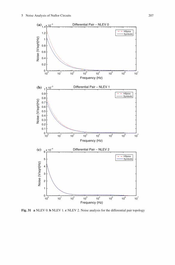
5 Noise Analysis of Nullor Circuits 207
HSpiceSymbolic
100
101
102
103
104
105
106
107
0
0.2
0.4
0.6
0.8
1
1.2
1.4x 10⁻³
Frequency (Hz)
Noi
se (
V/s
qrt(
Hz)
Differential Pair − NLEV 0
HSpiceSymbolic
100
101
102
103
104
105
106
107
0
0.1
0.2
0.3
0.4
0.5
0.6
0.7
0.8
0.9
1 x 10⁻³
Frequency (Hz)
Noi
se (
V/s
qrt(
Hz)
Differential Pair − NLEV 1
100
101
102
103
104
105
106
107
0
1
2
3
4
5
6x 10
−4
Frequency (Hz)
Noi
se (
V/s
qrt(
Hz)
Differential Pair − NLEV 2
HSpiceSymbolic
(a)
(b)
(c)
Fig. 31 a NLEV 0. b NLEV 1. c NLEV 2. Noise analysis for the differential pair topology

208 9 Symbolic Nodal Analysis of Analog Circuits Using Nullors
100
101
102
103
104
105
106
107
0
0.05
0.1
0.15
0.2
0.25
0.3
0.35
Frequency (Hz)
Noi
se (
V/s
qrt(
Hz)
Low Voltage Amplifier − NLEV 0
100
101
102
103
104
105
106
107
0
0.02
0.04
0.06
0.08
0.1
0.12
0.14
0.16
0.18
Frequency (Hz)
Noi
se (
V/s
qrt(
Hz)
Low Voltage Amplifier − NLEV 1
100
101
102
103
104
105
106
107
0
0.02
0.04
0.06
0.08
0.1
0.12
Frequency (Hz)
Noi
se (
V/s
qrt(
Hz)
Low Voltage Amplifier − NLEV 2
(a)
(b)
(c)
HSpiceSymbolic
HSpiceSymbolic
HSpiceSymbolic
Fig. 32 a NLEV 0. b NLEV 1. c NLEV 2. Noise analysis for the three stages uncompensatedamplifier

5 Noise Analysis of Nullor Circuits 209
The symbolic expression for the common source amplifier is then evaluated andplotted against the HSpice results in Fig. 30a for NLEV 0 and in Fig. 30b, c forNLEV 1 and 2, respectively. In Fig. 31 and Fig. 32 the responses for the differentialpair and the three stages CMOS amplifier are plotted for NLEV 0, 1 and 2.
As one sees, there is a good agreement between the numerical evaluation of thesymbolic expressions and the results provided by HSpice.
6 Summary
This chapter showed the analysis of analog circuits using nullors and pathologi-cal voltage mirrors and current mirrors. The formulation of this kind of circuits isperformed by pure Nodal Analysis (NA). The guidelines for formulating the NAequations were given and applied to CMOS amplifiers. The NA formulation canbe solved by applying the DDD, GPDD and the GBST discussed in the previoussections. The NA of analog circuits using nullors and pathological elements wasextended to perform symbolic sensitivity analysis as well as symbolic noise analysisof CMOS amplifiers, for which several examples were described to highlight theusefulness of this symbolic approach.

Part IIIApplications

Chapter 10Symbolic Moment Computation
1 Introduction
The analysis methods developed in the previous chapters are mainly for analyzinganalog circuits involving semiconductor transistors. The nonlinear transistor devicesare linearized for symbolic small-signal analysis. However, starting from the submi-cron fabrication technology around the year of 1990, the interconnect network as anintegral part in integrated circuits brought the designers’ attention because the inter-connecting wires could not be considered as simple capacitive or resistive elementsanymore. More accurate models must be used for precisely characterizing the signalbehavior as the signals are relayed by the wires.
Because of the massive connectivity existing in a full-chip, the traditional methodsof discretizing interconnects by lumped resistive (R), capacitive (C), and inductive(L) elements would generate enormous scale linear RLC networks for transistor-level circuit simulation, causing huge barriers to design verification. Pressed by thissituation, reduced-order modeling techniques arose as a fundamental technology forinterconnect modeling and analysis. This technology was considered as an essentialpart of semiconductor validation technology in the deep-submicron and nanometerregime of IC manufacturing.
In addition to the massive scale of interconnect networks in a single chip, processvariation was another challenging issue that emerged as the fabrication feature sizecontinued to downscale. The foremost challenge created by process variation wasfrom the need of establishing statistical timing models of interconnects. Geometricalvariations of interconnect dimensions could cause random fluctuation of electricalsignals as they propagate through the metal wires in different locations. Signal timingand crosstalk are important design metrics that must be analyzed and predicted withhigh fidelity while a full-chip is being placed, laid out and routed. These metrics, onceconsidered deterministic, have to be treated as stochastic quantities, thus creatingunexpected challenges to the traditional IC synthesis tools.
Reduced-order modeling was a classical concept firstly studied in the controltheory in the framework of linear systems; fairly complete theories have been
G. Shi et al., Advanced Symbolic Analysis for VLSI Systems, 213DOI: 10.1007/978-1-4939-1103-5_10,© Springer Science+Business Media New York 2014

214 10 Symbolic Moment Computation
developed in that discipline in the 1980s [12, 138]. The most popular reduced-order modeling method frequently used in the design automation community was theso-called moment-matching method [154, 164], which is computationally much eas-ier to implement within a general-purpose circuit simulator. Although a variety ofissues have been raised and addressed in the literature regarding passivity [144], real-izable reduction [193], and numerical computational issues [46], etc., this methodhas reached fairly high maturity and modern commercial circuit simulation toolshave started incorporating such techniques.
In spite of the great advancement of the reduced-order modeling technology, lessprogress has been made on statistical modeling of variational interconnect networks.Although the whole CAD community has been aware of the process variation issuesfor many years, the methods proposed in the open literature are so diverse that noadequate maturity has been reached yet. Some typical techniques proposed in thiscategory are: (i) Extension of the moment-matching-based reduced-order modelingtechniques to an ad hoc interval linear algebra, for which a number of approxima-tions are artificially introduced [124, 125]. (ii) A set of preliminary techniques forsymbolic model order reduction (SMOR) [205]. (iii) Variational analysis of intercon-nect circuits by combining the asymptotic waveform evaluation (AWE) method withadjoint sensitivity analysis [107, 270]. (iv) Extension of the moment methods forstatistical characterization of timing probability density functions (pdf) [4, 89, 279].(v) Definition of crosstalk noise metrics in terms of moments of the network response[25]. Some other works proposed implicit or explicit parametric moment matchingtechniques for variational interconnect analysis, such as [35, 114, 116].
So far, general interconnect networks, whether in tree forms or in mesh forms, havebeen modeled mainly by RC or RLC lumped networks. Because of the sheer numberof nodal voltages or branch currents involved in simulation, directly creating anoverall modified nodal analysis (MNA) matrix by stamping together all such lumpedelements would generate extremely high dimensional matrices badly conditioned,hence are hard to solve in a general-purpose simulator. Therefore, specific techniquesare needed to either remodel or fastly compute the electrical behaviors of the lumpednetworks so that the challenging full-chip verification tasks can be finished in areasonable duration of time.
The work developed in this chapter takes a symbolic approach to statistical analysisof variational interconnect networks. As we have implicitly indicated in the earlierchapters, symbolic network analysis is targeted at generating analytical responsefunctions in the frequency domain, for which input–output ports must be defined apriori. However, it is typical that in almost all interconnect analysis problems, wehave to deal with multiple driving sources and multiple output points, such as a clocktree or multiple-source driven clock meshes. It is much harder to create reduced-ordermodels for such multiple input–output networks in general [269]. In the meantime,directly developing a symbolic network functions for such networks is also muchmore challenging.
The symbolic analysis techniques we are going to develop in this chapter arenot simple extensions of the traditional techniques by directly creating symbolicnetwork function, as we have done in the earlier chapters. Instead, we shall take an

1 Introduction 215
approximation approach by symbolically computing the moments. Such momentscan be used in creating a variety of metrics to characterize the network electricalproperties. Hence, this approach not only saves a great amount of computationalcomplexity, but also retains its applicability.
The main content of this chapter is based on the notion of “symbolic moments”and to develop a generic construction method for a Symbolic Moment Calculator(SMC). The developed construction method is applicable to a variety of intercon-nect configurations, including trees, coupled-trees, and meshes, all can be driven bymultiple independent sources. The SMC will be constructed as a Binary DecisionDiagram (BDD) data structure, whose advantages are to be explained in the sequel.
With SMC, it is only necessary to construct a data structure for computing the0th-order of moments. Other higher orders of moments then are computed by reusingthe existing data structure. The construction is based on circuit tearing and sub-circuitsharing. Therefore, only the network structure has to be manipulated when creatingan SMC. We shall show that this novel construction method is of cubic polynomialcomputational complexity, instead of exponential complexity required for creatingexact symbolic representations. Due to the reduced complexity, this method canbe applied to fairly large interconnect networks for parametric timing and signalintegrity analysis.
Recursive computation lies at the core of moment computations, which is well-known in particular for tree-structure RLC networks. Some recursive formulas knownin the literature for moment computation are reviewed in Sect. 2. Since the momentsfor tree circuits are computed by additive and multiplicative operations, the recursiveformulas can be reformulated in the form of BDD data structure. When some nodesin a tree-structured network are connected by resistors forming resistive loops, theunderlying computation principle valid for recursive computation breaks down. Suchresistive links have to be decomposed by using the Kron’s branch tearing techniqueintroduced in Sect. 3. Fortunately, a number of subcircuits resulting from tearinghave common structure, hence can be shared by a BDD. This mechanism is themost important innovation in adapting a symbolic method for interconnect networkanalysis. Successive decompositions of all resistive links would end up with a singletree network, but possibly driven by a variety of current sources placed at someselected tree nodes. Then the moments are computed in a bottom-up fashion by whichthe repeated computations are reduced to minimum because of common subnetworksharing. The same tearing technique can be applied to the moment analysis of meshnetworks driven by multiple sources. Section 4 studies the computational issues formoment sensitivity. The efficiency of the SMC technique is evaluated in Sect. 5.Section 6 concludes this chapter. The main contribution of this work is based on therecently published work [77]. It once again demonstrates the powerfulness of usingBDD for symbolic moment computation.

216 10 Symbolic Moment Computation
2 Moment Computation by BDD
RLC circuits are linear networks whose behavior can be described by lineardifferential equations in the following state-space form
Edxdt
+ Ax = Bu, (1a)
y = Fx, (1b)
where x ≤ Rn is the circuit state vector consisting of nodal voltages and branchcurrents, u ≤ Rr is a vector standing for the input voltage/current sources, andy ≤ Rq is the vector of measurements. The coefficient matrices E, A, B, and F areof compatible dimensions and, in particular, the matrices E and A are respectivelysusceptance and conductance matrices of a passive network. The matrices B and Fare defined by the placement of input sources and output measurements, thereforeare special matrices consisting of elements 1, −1, and 0.
Applying Laplace transform to (1a), (1b) we obtain the frequency-domain transferfunction of the network from the input u to the output y
H(s) = F (Es + A)−1 B, (2)
which is a matrix function of the Laplace parameter s. Assuming that A is invertible,we may rewrite
H(s) = F(
A−1Es + I⎡−1 (
A−1B⎡
, (3)
where I is an identity matrix of proper dimension.Expanding the function H(s) into a series of sk , we get
H(s) =∈⎢
k=0
(−1)kmksk = m0 − m1s1 + m2s2 − m3s3 + · · · , (4)
where
mk = F(
A−1E⎡k (
A−1B⎡
(5)
is called the kth order input/output (I/O) moment of the network given the selectedinput–output ports [154].
It is well-known that a number of electrical properties of a linear network canbe derived from the moments. Hence, developing efficient moment computationprocedures is of great interest in practice. A commonly used approach is to computethe moments recursively, for which we define
μ0 = A−1B,μk =(
A−1E⎡
μk−1, (6)

2 Moment Computation by BDD 217
in
1
2
3
LR2 2
C2
C1
LR1 1
LR
C
3 3
3
6LR6 6
C6
4LR
C4
44
5LR
C
5 5
5
V
Fig. 1 An RLC tree
where μk ≤ Rn, k = 0, 1, 2, . . ., are called the kth order state moments. Then the I/Omoments mk are calculated by mk = Fμk . Note that the state moments characterizethe internal electrical behavior of a network, while the I/O moments characterize theexternal electrical behavior.
We notice that the computation of the state moments defined in (6) requires invert-ing the matrix A. In terms of circuit simulation it is equivalent to a dc solution of thelinear network given appropriate sources. Hence, in this sense a numerical SPICEsimulator can be used to compute both state and I/O moments.
However, if we would like to compute the moments symbolically, it seems thatwe have to deal with the issue of symbolically inverting the matrix A. Directlyinverting a matrix analytically is a computationally intractable problem in general.Except for some specially structured matrices, hardly any symbolic circuit analysismethod reported in the literature takes on this approach [205]. Nevertheless, as wehave experienced in the previous chapters, if we address the symbolic computationproblem from the perspective of I/O responses, then the moments as defined abovecan be computed for quite a large class of interconnect circuits.
2.1 Moment Computation for Tree Circuits
We first review on how the moments are computed for tree-structure networks, whichcommonly appear in digital integrated circuits. After learning the basic principlesinvolved in the computation, we may readily extend such formulas to other networkstructures, such as several tree networks coupled capacitively and/or inductively.
The tree-structured RLC network shown in Fig. 1 has regular connections. Everyserial R-L branch has a connection to the ground via a grounding capacitor. The state-space model in the form of (1a) and (1b) has the following coefficient matrices:

218 10 Symbolic Moment Computation
E =⎣
C 00 L
⎤
, A =⎣
0 A−AT R
⎤
, B = −⎣
0e1
⎤
,
F = ⎥IN 0
⎦,
where C and L are diagonal matrices comprising of the capacitances Ci andinductances Li, respectively, and R is also a diagonal matrix comprising of the resis-tances Ri. The first half of the state vector x contains the nodal voltages for the nodesgrounded by the capacitors, and the second half contains the branch currents for thecurrents flowing through the serial R-L branches. N is the total number of nodesgrounded by the capacitors, which is also the total number of R-L-C sections. All thenodal voltages (i.e., the first half of the state vector) are considered as the outputs.The matrix A is the incidence matrix of the serial R-L branches in the network, thematrix IN is the N-dimensional identity matrix, and e1 is the first column of thematrix IN , i.e., the first basis vector of RN . For the given circuit shown in Fig. 1,the input source vector u is just the voltage source Vin. In case the network is alsodriven by current sources driving the nodes connected by the Ci’s, we can modifythe input matrix B and the input source vector to incorporate the independent currentsources.
For an RLC tree as given in Fig. 1, by node i we refer to the node connected tothe grounding capacitor Ci. Suppose the tree is driven by an arbitrary voltage sourceVin at the input node. Let Vi(s) be the Laplace transform of the voltage response atnode i. For each Vi(s) we can Taylor-expand it into a series like (4). Let mi,k be thekth order (voltage) moment at node i. It is known that the nodal voltage moment mi,k(k ∧ 2) can be computed recursively by the following formula [164, 272]:
mi,k =⎢
Rα≤Pi
Rα
⎢
j≤Tα
Cj · mj,k−1 −⎢
Lα≤Pi
Lα
⎢
j≤Tα
Cj · mj,k−2, (7)
where Pi represents the path from the tree root to node i, the summation over Rα ≤ Pi
means to sum over all the resistors Rα on the path Pi, the notation Tα in the summationindex denotes the subtree starting from the root at node α and including the rest, andthe summation over j ≤ Tα means to sum over all nodes belonging to the subtree Tα
(including the root of Tα). The first two orders of moments are
mi,0 = 1 and mi,1 =⎢
Rα≤Pi
Rα
⎢
j≤Tα
Cj, (8)
for i = 1, . . . , N . Note that the 0th order moment is the dc solution of the originaltree circuit, and the first order nodal moment mi,1 is the Elmore delay from the inputto the node i [160]. If there exist independent dc current sources connected in parallelto the capacitors, then the 0th order moments can be calculated by the principle ofsuperposition. The independent dc sources only affect the evaluation of the 0th ordermoments, but are not involved in the computation of the higher order moments.

2 Moment Computation by BDD 219
We see that formula (7) involves two summation terms of the same form∑
j≤TαCj ·
mj,k−1 corresponding to the two moment orders (k −1) and (k −2). For conveniencewe denote such a summation term by
mCα,k =
⎢
j≤Tα
Cj · mj,k−1, (9)
and call it the capacitor moment (or C-moments) because the Cj’s are involved. Thequantity of mC
α,k can be interpreted as an accumulative “current” entering node i dueto the current sources of magnitudes Cj · mj,k−1.
It is computationally helpful to observe that the summation∑
j≤Tα(·) over the tree
Tα is always fixed in the computation of the different orders of moments. What isbeing substituted is the summand of the form Cj · mj,k−1, which is always in theform of a moment multiplied by Cj, which can be considered as a substitution of thecapacitance Cj. This observation is of importance when we create a data structurefor symbolic moment computation. We only need to create a data node for eachCj and substitute it by other quantities like (Cj · mj,k−1) when needed. All othercomputational structures implemented for summation, etc. do not have to be altered.
With the new notation defined in (9) the moment recursion formula (7) can bewritten as
mi,k =⎢
Rα≤Pi
Rα · mCα,k −
⎢
Lα≤Pi
Lα · mCα,k−1, (10)
where both summations are over the path Pi from the tree root to node i. If we viewthe C-moments mC
α,k as current sources, the first summation in (10) is just the sum of
voltage drops passing the resistors on the path Pi, while the term∑
Lα≤PiLα ·mC
α,k−1 isjust the sum of voltage sources “generated” when the currents passing the inductorsalong the path Pi. Hence, Eq. (10) is simply the result of applying Kirchhoff voltagelaw (KVL) to the path from the driving input to the observation point at node i.While computing the moments for k ∧ 1, the driving voltage Vin is switched off,i.e., Vin = 0.
We observe that a tree is a branching structure. Therefore, when a computationis performed from the root toward node i on the tree, it can be performed in arecursive manner. In other words, some quantities computed earlier can be reusedby the computation of the subsequence quantities. This principle can be applied tothe following reformulation of formula (10).
Let p(i) be the parent node of node i in that node i is a fanout of node p(i). Thenthe moments computed progressively from the tree root up to node p(i) can be usedfor the computation of the succeeding moments at the nodes fanning out from nodep(i). With the fanout notation, the recursion formula (10) can be rewritten as
mi,k = mp(i),k + Ri · mCi,k − Li · mC
i,k−1, (11)

220 10 Symbolic Moment Computation
Fig. 2 Illustration of a BDDtriple
p(i)RCi
Li
Ci
Lp(i)
iR
which means that the computation of all orders of moments at any node i fanningout from node p(i) can make use of the foregoing moment mp(i),k computed at theparent node p(i).
Equation (11) can be decomposed into two parts
mRi,k := mR
p(i),k + Ri · mCi,k, (12a)
mLi,k := mL
p(i),k − Li · mCi,k−1, (12b)
so that mi,k = mRi,k + mL
i,k . We simply refer to mRi,k and mC
i,k as resistor moments (orR-moments) and inductor moments (or L-moments), respectively.
The computation of both right-hand sides in (12a), (12b) involve one multipli-cation and one addition/subtraction, which reminds us of a BDD triple we haveencountered in the earlier chapters. A BDD triple is a graphical representation ofthree vertexes connected as in Fig. 2, in which a solid arrow stands for multiplicationand a dashed arrow for addition/subtraction. In the figure, a vertex named by Ci
computes a quantity like (Cj · mj,k−1) in the capacitor moment defined by (9) whilea vertex named by Ri or Li respectively computes the expression defined by (12a) or(12b). When computing the right-hand side of (11), we just subtract the top vertexnamed by Li from that named by Ri.
Interconnecting such triple vertices as shown in Fig. 2 creates a Binary DecisionDiagram. BDD is such a data structure that common computations are performed onlyonce, which is particularly suitable for the moment computation of a tree-structureRLC circuit.
Shown in Fig. 3 is a symbolic moment calculator for the tree circuit given inFig. 1. This computation diagram consists of two parts: The lower part in Fig. 3consist of the circled Ci’s connected by dashed arrows, it computes the C-momentsdefined by (9). As the formula indicates, the computation of the C-moments is basedon a tree. The kth order capacitor moment at node α, mC
α,k , is a summation of theterms Cj · mj,k−1 over the subtree Tα rooted at node α. The moment mj,k−1 has beenpreviously calculated and is supposedly saved with the node named by Cj. Becausethe computation is tree-based, we only have to create a set of C-nodes and connectthem in the same structure as the original circuit. This part of data structure is calleda C-tree hereafter, which performs the computation of the capacitor moments bybottom-up traversals. We note that this part of computation is not BDD.
After the capacitor moments have been computed and saved in the nodes in theC-tree, these quantities will in turn be used to compute the two sets of moments mR
i,k

2 Moment Computation by BDD 221
Fig. 3 SMC structure for atree circuit
4R
6R5R
2R
3R
1R
C1
C3
C2
C4
C5 C6
0
and mLi,k defined in (12a), (12b). This part of computation is performed in BDD form
and is executed by the upper half of the diagram shown in Fig. 3.We see that the circled Ri nodes in the upper half are connected by dashed arrows
as well, each directing toward a parent node. These dashed arrows are BDD arrows,hence they perform additions/subtractions. The R-nodes are connected in a treeconfiguration identical to the original tree circuit. In addition, the R-nodes have solidarrows connecting to the C-tree nodes in one-to-one fashion; namely, Rk points toCk for all k. For R1 at the tree root, it has a dashed arrow connecting to the BDDterminal “0”. Remember that those solid arrows connecting from the R-nodes to theC- tree nodes would perform the multiplications defined by (12a). We have said thatthe capacitor moments mC
i,k are stored with the C-nodes. Therefore, it is trivial toverify that the connections defined for the R-nodes would compute the R-momentsdefined by (12a). A computation diagram for the L-moments defined by (12a) isexactly similar to that for the R-moments. One may choose to reuse the R-nodes forcomputing the L-moments in implementation.
Because both parts formed by the R-nodes and C-nodes in Fig. 3 just have thetree structure configuration identical to the original circuit, creating an SMC datastructure for them is fairly easy. It is also trivial to add appropriate arrows as wehave defined for the purpose of moment computation. Because the R-nodes form aBDD, it is called an R-BDD. Similarly, we can obtain an L-BDD by replacing all theR-nodes in an R-BDD by L-nodes. An L-BDD would perform the computation ofEq. (12b).
Since the SMC as shown in Fig. 3 is created for computing the moments of atree circuit, it is hereafter called a tree-SMC. Later, we shall extend the principleinvolved with an SMC to other more complex circuit structures. Remember that anSMC consists of a tree-structured BDD involving R-nodes or L-nodes, and a C-tree.
We summarize here how different orders of moments for an RLC tree circuitare computed with a tree-SMC. The 0th-order moments at all tree nodes, denotedby a vector m0 = (m1,0, . . . , mN,0)
T , is the dc solution of the tree circuit drivenby a unity dc voltage source at the input (or root). The first-order moment vector

222 10 Symbolic Moment Computation
m1 = (m1,1, . . . , mN,1)T is computed by traversing the C-tree bottom-up once and
save the first-order C-moments mCi,1 in the C-tree nodes. Then we compute the R-
moments by traversing the R-BDD vertices from bottom-up. If the circuit has induc-tors, then the L-moments mL
i,k are computed by setting the C-tree nodes to the values
of the one-order lower moments mCi,k−1 and traversing the L-BDD vertexes bottom-
up. Subtraction of the moments at the corresponding R-BDD and L-BDD verticesproduces the moments mi,k for i = 1, . . . , N .
Because the computation of one order of moments is completed by one round ofSMC traversal, the computation complexity is proportional to the number of R-type(or L-type or C-type) elements. Suppose a tree network containing N segments ofRLC, the complexity is O(N). If up to the ρth order moments are requested, thecomputation time complexity is O(Nρ). Therefore, the moment computation for treecircuits is of linear complexity.
2.2 Moment Computation for Coupled Trees
In digital IC design we usually need to consider the crosstalk between interconnectsfor studying the issue of signal integrity. One feasible way of modeling the crosstalkphenomenon is to consider capacitively and inductively coupled RLC trees. Suchcircuits can be analyzed by moments as well. Introduced in this section is an extensionof the SMC method to coupled tree circuits.
As before, we shall follow the basic principle by viewing the coupling capacitorsas current sources and the coupling inductors as voltage sources. This perspectivecan help to justify the physical meaning of the derived current/voltage equations.We shall see that the coupling capacitors and inductors just add extra driving currentand voltage sources to each individual tree, which can easily be incorporated in themoment computation formulas derived earlier for tree circuits.
We shall be using the following notations for describing the method. Each indi-vidual tree is labeled by a Greek superscript, say, Tα stands for the αth tree. Thesuperscripts labeled to the elements indicate which tree the elements belong to. Thejth node in the tree Tα is denoted by nα
j . By convention, a tree node always refersto a node where a grounding capacitor is connected. Let Pα
j refer to the path fromthe root, denoted root(α), of tree Tα to node nα
j . A coupling capacitor connecting
nodes nαi and nβ
j is denoted by Cα,βi,j . An inductive coupling is modeled by a mutual
inductance Mα,βi,j = Kα,β
i,j
√Lα
i · Lβj , where Kα,β
i,j is the mutual inductance coefficient,
and Lαi and Lβ
j are two inductors located in two separated trees Tα and Tβ . Figure 4
shows an example of two coupled RLC trees rooted at V1s and V2
s .The nodal voltage moments for coupled trees can be expressed by the following
recursive formulas similar to the expressions in (9) and (10) [104]:

2 Moment Computation by BDD 223
root(2)
R11
1L1
C11
R21 L2
1
C12
L31
R31
C31
R41 L1
4 C14
V 2s
1Vs
R21 L
21
C21
R2
3
C32
L23
C1,11,2
C2,21,2
C3,31,2
2,21,2
K1,11,2K 3,3
1,2K
R22 L2
2
C22
root(1)
Fig. 4 Two RLC trees coupled
mαj,k =
⎢
Rαα ≤Pα
j
Rαα · mC,α
α,k −⎢
Lαα ≤Pα
j
⎛
⎧⎪Lα
α · mC,αα,k−1 +
⎢
Lβ
α⊆ ≤Lαα
Mα,βα,α⊆ · mC,β
α⊆,k−1
⎨
⎩⎠ , (13a)
mC,αj,k =
⎢
nαα ≤Tα
j
Cαα · mα
α,k−1 +⎢
nαα ≤Tα
j
⎢
Cβα⊆ ≤Cα
α
Cα,βα,α⊆
(mα
α,k−1 − mβα⊆,k−1
⎡, (13b)
where mαj,k denotes the kth order moment at node nα
j and mC,αj,k denotes the kth
order capacitor moment (C-moment) at node nαj . The notation Cα
α in the summationindex denotes the set of coupling capacitors connected at node nα
α , and the notationLα
α denotes the set of inductors mutually coupled with the inductor Lαα . The other
summation indices are self-evident.In (13a) the term Mα,β
α,α⊆ ·mC,βα⊆,k−1 generates a voltage in the path where the inductor
Lαα locates due to the coupling inductors. In (13b) the term
(mα
α,k−1 − mβα⊆,k−1
⎡
in (13b) is the voltage difference across the coupling capacitor Cα,βα,α⊆ , which after
multiplying the coupling capacitor Cα,βα,α⊆ generates a current from node nβ
α⊆ to nodenαα .
Equation (13a) also can be rewritten in a recursive form as
mαj,k = mα
p(j),k + Rαj · mC,α
j,k − Lαj · mC,α
j,k−1 −⎢
Lβ
j⊆ ≤Lαj
Mα,βj,j⊆ · mC,β
j⊆,k−1. (14)
This recursive formula suggests us again that the moment for coupled trees also canbe computed by a BDD.
A little inspection of the formulas in (13a), (13b) shows that the formulas wouldreduce to the moment computations of individual trees if the couplings are removed,while the inductive and capacitive couplings just generate additional terms by using

224 10 Symbolic Moment Computation
00
1R12R1
3R1
C11
1R2
C12
C22
C21
C31
C41
C32
4R1
2R23R2
M1,2
1,1
M1,2
2,2 M3,3
1,2
3,3
1,2C
1,2C
2,2
1,2C
1,1
Fig. 5 SMC for two coupled trees
the previously computed moments. Hence, once again a graphical construction pro-cedure can be formed as follows: First, construct SMC diagrams for the individualtrees. Then, add coupling links between the L-nodes of the SMC diagrams for induc-tive coupling and between the C-nodes for capacitive coupling.
For an illustration, Fig. 5 shows the SMC for computing the moments of thecoupled RLC tree circuit given in Fig. 4. We see two sub-structures in the left halfand right half, which are connected by the double-arrow dashed lines that stand forcoupling. The coupling parameters like Cα,β
α,α⊆ and Lα,βα,α⊆ are attached to the double-
arrow dashed lines. The node names are just the circuit element names. Note thatthe R-nodes can be replaced by L-nodes when computing the inductor related terms,because they have the same computational structure.
Clearly, the overall SMC is composed of two coupled tree-SMC’s, each computingthe moments of each individual tree. Because the previously computed moments arestored with the tree-SMC nodes, the coupling term of
∑Lβ
j⊆ ≤Lαj
Mα,βj,j⊆ · mC,β
j⊆,k−1 in
(14) and∑
Cβα⊆ ≤Cα
α
Cα,βα,α⊆
(mα
α,k−1 − mβα⊆,k−1
⎡in (13b) can be computed easily by the
double-arrow connections drawn in the SMC.To begin the SMC computation, the 0th order moments of all nodes are computed
as the dc solution of the coupled circuit by ignoring the inductive and capacitivecouplings. The dc moments are then used for computing the higher order moments.We note that no extra computational nodes need to be created for the inductive andcapacitive couplings, except that extra quantities coming from the coupling linksbetween the tree-SMCs have to be incorporated in the computation.
3 Mesh Circuits with Multiple Sources
By mesh circuits we refer to RC networks with resistor loops while all nodes aregrounded via capacitors or driven by non-ideal voltage sources. The previously stud-ied uncoupled RLC tree circuits or coupled tree circuits do not involve resistiveloops. When a circuit has resistor loops, the capacitor moments (C-moments) cannot

3 Mesh Circuits with Multiple Sources 225
be computed by recursion on the tree branches. However, mesh circuits widely existin digital integrated circuits, such as clock meshes or power/ground (P/G) networks[161, 165]. More recently, clock mesh analysis and synthesis are receiving increasingattentions [24, 162, 269]. A mesh network could be driven by many sources at theselected mesh nodes. Synthesis and verification of mesh networks require efficientanalysis methodology and algorithms instead of repeatedly running SPICE simula-tions. Several works have already attempted to use model order reduction techniquesfor synthesizing clock meshes, but encountered difficulty in handling multiple drivingsources [24, 269].
In this section, we shall develop a symbolic moment computation method capableof analyzing mesh networks driven by multiple sources. For simplicity but withoutlosing applicability, we exclude inductors in the following development.
The key technique we shall use in this section is called branch tearing, whichwas proposed by Kron [99] in 1939 and later reinterpreted by Rohrer [168] in 1988.Kron’s branch tearing works as follows: By selecting a resistor link Rlink a network isdecompose into two networks, one network does not contain Rlink while in the othernetwork the Rlink is replaced by a current source. Recombing the solutions of thetwo decomposed networks by superposition regenerates the solution to the originalnetwork.
For a mesh circuit, we can select a set of resistive links; by removing all such links,the mesh becomes a spanning RC tree. We then apply a sequence of Kron’s tearingsuccessively to the set of resistive links. While the mesh circuit is being decomposed,the resulting networks are saved after checking whether common networks can beshared. In the course a BDD data structure is created to save the sequence of decom-positions. A little algebraic analysis would suggest us that the BDD structure alsocan be used for moment computation by running bottom-up traversals. The currentsource replacing a torn link will finally appear as a driving source in the RC spanningtree circuit. The SMC established earlier for tree circuits can be used for all momentcomputations.
3.1 Kron’s Tearing and Mesh Decomposition
Kron’s branch tearing technique was first applied to handle resistor links for fastmoment computation in the RICE work [164] published in 1994. Later Lee et al.[105, 106] proposed to use a BDD to represent the decomposition process by tearingresistive links. The work [75, 76] further formulated a full symbolic framework formoment analysis of mesh networks driven by multiple sources.
The principle of Kron’s branch tearing is illustrated by the circuit shown in Fig. 6.The circuit has a single driving current source Is1. The resistor R3,6 connected betweennodes 3 and 6 is selected as a resistor link. By removing this link the circuit becomesan RC spanning tree.
According to the principle of Kron’s tearing, solving the circuit shown in Fig. 6 canbe performed by solving two modified RC-tree circuits: one is obtained by removing

226 10 Symbolic Moment Computation
s1
C6
C1
C5
R6
C4
R3
C2 C3 R3,6
R5R4
R21 2 3
4 5 6R
Is1
Fig. 6 A resistive link R3,6 is inserted to a tree circuit
s1
C6
C1
C5
R6
C4
R3
C2 C3
R5R4
R21 2 3
4 5 6I Rs1
s1
C5
R6
C4
R3
C2 C3
R5R4
R2
C6
IR
C1
1 2 3
4 5 6
−IR
I Rs1
(a)
(b)
Fig. 7 a Circuit with R3,6 removed. b Circuit with R3,6 replaced by the current source IR
the R-link R3,6 as shown in Fig. 7a, while the other is the result of replacing theR-link R3,6 by a current source of magnitude IR as shown in Fig. 7b. For the secondcircuit the current source IR is connected as two grounded current sources of oppositepolarity.
The magnitude of the current source IR is calculated as follows. Let Rlink = Rp,q
be the resistor link connecting between nodes p and q, which is to be replaced by acurrent source. Before calculating IR, we assume that the circuit without Rlink (calledlink-opened circuit) has been solved with all independent sources on. Let V (O)
Rlinkbe the
cross voltage at the terminals of Rlink (oriented from p to q). (We use the superscript(O) to indicate the link-opened case.) Then, the magnitude of IR is computed by (seea derivation in [168] based on the Householder Theorem)
IR = V (O)Rlink
Rlink + RTH, (15)

3 Mesh Circuits with Multiple Sources 227
where RTH is the Thevenin equivalent resistance seen at the port of Rlink . IR will beconnected to the circuit in the same orientation as V (O), i.e., from p to q.
The Thevenin equivalent resistance RTH can be calculated by applying a unitycurrent source in place of Rlink and measuring the port voltage where Rlink is removed.The nodal voltages of the unity-current driven circuit will also be used for superposinga full solution of the original network. Therefore, we denote V (A)
i the voltage at nodei for the unity-current driven circuit, where the superscript (A) just refers to theunity-current IR = 1A applied as the only independent source. For the example weare considering, this circuit is the one shown in Fig. 7b with IR = 1A while Is1 isswitched off. Given the solution of all V (A)
i , the Thevenin resistance is then calculatedas the port voltage, i.e.,
RTH = V (A)p,q = V (A)
p − V (A)q . (16)
With the quantities V (O)i , V (A)
i , and IR solved, the nodal voltages of the originalcircuit with the resistor Rlink placed back are computed by superposition [168]:
Vi = V (O)i − IR · V (A)
i , (17)
for i = 1, . . . , N , where N is the total number of mesh nodes. The voltages Vi arethe 0th order moment of the original circuit.
Regarding the computation, we shall use the SMC created for the tree circuit asfollows. When we need to compute the nodal voltages driven only by a unity currentsource replacing the torn link, we just set Cp = Cq = 1 in the C-tree while setting allother capacitors to zero. Note that Cp and Cq are just the two capacitors connectingthe two terminals of the torn resistor to the ground. When we have more links to tear,the tree-based SMC will be invoked as many times as the number of resistor links,which is to be discussed in the next section. Remember that a tree-SMC has to beconstructed only once but will be used for many computations, which is a typicalfeature by symbolic computation.
We summarize that each step of Kron’s tearing involves two operations: solving a“1A-source driven” circuit and solving a “link-opened” circuit, which is apparentlybinary decision-making. It is appropriate to use a BDD for the data management inthe tearing process. If we have more than one link to tear, a sequence of such binarydecisions will be made. Moreover, as the tearing goes on, many intermediately torncircuits are common and can be shared. Hence, in the next section we shall see thatBDD is the most suitable data structure for representing the process of Kron’s tearing.This idea was first contributed by Lee et al. in [105, 106].
3.2 Moment Computation for Mesh Circuits
A mesh circuit could have many resistive links, including those resistors in series withnon-ideal voltage sources driving a portion of mesh nodes. Such non-ideal voltagesources can be equivalently represented by ideal current sources connected in parallel

228 10 Symbolic Moment Computation
s2
3
C2 C3 R3,6
R2
I s1 R4
R 6R5
C1
I s2C 6C5C4
1 2 3
Rs1
4 5 6
R
R
Fig. 8 A mesh circuit with multiple sources
Fig. 9 Tearing-BDD for thecircuit given in Fig. 8
(O, O)
Rs2
(A, R )s2
R3,6
Rs2
(O, R )s2
3,6(R , R )
s2
(O, A)(A, O)
Open
1A
1A
Open1AOpen
with the source resistors in the form of Norton equivalence. Figure 8 shows suchan example, in which Is2 and Rs2 model a non-ideal driving voltage source appliedat node 4. The recursive moment computation principle again breaks down if thereexists a grounding resistor in a tree circuit. The grounding resistor must be torn inorder to apply recursive computation. By tearing, one unity current source directedfrom the driving node to the ground has to be placed.
When a mesh circuit has more than one resistive links, a sequence of tearing willbe performed in order to remove all link resistors, and in the course some intermediatecircuits are shareable. For the example given in Fig. 8 with two current sources, weselect the current source Is1 as the driving source of a selected spanning tree network,and will tear the grounding resistor Rs2 and the link resistor R3,6. The two steps oftearing are saved in the diagram shown in Fig. 9, which is in the form of a BDD. Ateach BDD vertex a tuple is attached which flags the state of the circuit for the nextstep of tearing downward.
The notation used in Fig. 9 is quite different from that in [105], it should be mucheasier to follow. The tuple (R3,6, Rs2) written at the BDD root means that we havetwo resistors R3,6 and Rs2 to tear in the listed order. The tearing of the resistor R3,6results in the two circuits marked by the tuples (A, Rs2) and (O, Rs2), which labelthe two BDD vertices in the second row. The tuple (A, Rs2) means that the resistorR3,6 has been replaced by a unity current source (1A). Remember that, when a unitycurrent source is applied to the circuit, all other independent current sources must beswitched off because we are using the superposition principle. On the other hand, the

3 Mesh Circuits with Multiple Sources 229
tuple (O, Rs2) means that the resistor R3,6 has been removed while all independentsources are retained.
In the next step we tear the resistor Rs2 in a similar manner. We have two interme-diate circuits to work with, which are owned by the two BDD vertexes in the middlelayer of Fig. 9. The first circuit is denoted by (A, Rs2). Tearing of Rs2 generatestwo more circuits denoted by (A, O) and (O, A) in the bottom layer: the first circuit(A, O) means a circuit with R3,6 still substituted by the 1A source but Rs2 is now tornopen, and the second circuit (O, A) means that Rs2 is now replaced by a 1A sourcebut all other sources are switched off. Therefore, whenever we see an ‘A’ in a tuple,the other entries must be ‘O’.
Then we look at the circuit denoted by (O, Rs2) owned by the right BDD vertexin the middle layer, which also generates two more circuits after tearing. When Rs2is replaced by an 1A source, the resulting circuit is again (O, A), which shares withthe previously created one. When Rs2 is torn open, we get the circuit (O, O), whichmeans that both link resistors have been torn off, but all the independent sourcesremain. We have framed the rightmost tuple (O, O) in the bottom layer in Fig. 9 toraise the reader’s attention, because this is the only circuit we shall access to updatefor computing higher-order moments.
Consequently, the tearings of the two circuits in the middle layer have generatedthree circuits in the bottom layer of Fig. 9. These three circuits, denoted by (A, O),(O, A), and (O, O), are all tree circuits but driven by different sources. The firsttwo are driven by a single unity current source substituting R3,6 or Rs2, respectively,while the third is driven by all independent sources existing with the original circuit.Although these tree circuits are driven by different sources, the trunk circuit (byignoring the sources) remains the same. Therefore, we only need to create one SMCfor the spanning-tree circuit with all nodes grounded by capacitors. Whenever itneeds to compute a solution with respect to one specific case of driving sources, wejust substitute the capacitors by the corresponding sources and run the SMC once.
The BDD shown in Fig. 9 is called a tearing-BDD. There exist several regularfeatures with all tearing-BDDs which are worth mentioning: Firstly, all BDD vertexesin the same layer have the same name of the resistor torn. Although the torn resistorexists in several different circuit configurations, when it is substituted by a unitycurrent source, the resulting circuit is identical, because all other sources are switchedoff. Therefore, one BDD vertex in any layer (other than the top layer) must be sharedby all solid arrows coming down from the preceding layer, which becomes the secondfeature. Knowing these properties can greatly simplify the construction of a tearing-BDD.
3.3 High-Order Moments
In addition to representing the sequence of Kron’s tearing in the form of a tearing-BDD, each BDD vertex must perform the computation defined by the formulas (15),(16), and (17) for the 0th order moments. The computation is performed bottom-up as

230 10 Symbolic Moment Computation
follows: The circuits at the bottom of the tearing-BDD are solved first by repeatedlyrunning the SMC for a tree circuit with different driving current sources. Then thecomputation propagates upward by superposing the circuit solutions obtained at twochild vertices. The child vertex pointed by the (solid) 1A-arrow is used to calculateRTH . Then the resistance value saved in the parent vertex together with RTH andthe solution from the child vertex pointed by the (dashed) Open-arrow are usedto calculate IR by (15). Finally, the calculated IR and the circuit solutions fromboth child vertexes are used to calculate all nodal voltages of the current circuit bysuperposition (17). The solved solution is saved with the parent vertex. When theroot vertex is reached, the 0th order moments of the original circuit at all nodes havebeen computed.
Because mesh circuits have capacitors, we can compute higher order momentsby applying the same principle as that of tree circuits. That is, the computation ofthe next order moments is performed by substituting the capacitors by appropriatesources as in the definition of C-moments in (9). The substituting current sourcesact as independent sources; when the network is driven by a 1A-current source asa replacement of a torn resistor, all the substituting sources for the capacitors mustbe switched off. Therefore, during the computation of all higher-order moments,all those intermediate circuits marked by the tuples containing a single A do notneed to be recomputed, because they remain unaltered. Hence, their computationsare performed only once regardless of what moment order is being computed. Con-sequently, updating the capacitor nodes by the previously computed moments andusing them as independent sources have to be performed only for the circuit markedby a tuple of all O’s in the bottom layer of the tearing-BDD, which is the rightmostone in Fig. 9.
The feature we have pointed out above could save a great amount of computa-tion in practice, which is another advantage of using SMC for symbolic momentcomputation.
In summary, the computation of the kth order moment at node i (i = 1, . . . , N) fora mesh circuit is performed by the following formulas, assuming that the resistivelink Rlink is connected between nodes p and q. Since RTH is independent of themoment order, we assume that it has been computed during the computation of the0th order moments and saved with its own BDD vertex. In fact, all vertexes in eachlayer of tearing-BDD have the identical RTH because their solid arrows labeled by 1Aall point to the same circuit in the next layer. Therefore, we only need to update thequantities IR,k and mi,k by the following two equations, where the second subscriptk stands for the kth order of moments:
IR,k = m(O)p,k − m(O)
q,k
Rlink + RTH, (18a)
mi,k = m(O)i,k − IR,k · m(A)
i . (18b)
Again the superscripts (O) and (A) indicate whether to get the respective quantitiesfrom the dashed arrow or the solid arrow accordingly in the tearing-BDD.

3 Mesh Circuits with Multiple Sources 231
3.4 The SMC Algorithm
The computation performed by an SMC for a tree circuit together with the traversalsthrough a tearing-BDD is generally called Symbolic Moment Computation. The keysteps of the developed algorithm are summarized below.
Symbolic Moment Computation Algorithm
Step 1. Select one primary source and find a spanning tree rooted at the source,which spans the original circuit. Save the removed link resistors in a set.
Step 2. Construct an SMC diagram for the spanning RC-tree by assuming that allnodes are grounded via capacitors.
Step 3. Construct a tearing-BDD for all the link resistors and the grounding resis-tors (if any) in an arbitrary order.
Step 4. Evaluate the bottom vertices of the tearing-BDD, which are marked by atuple involving a single ‘A’, which represents the spanning-tree circuit driven bythe only unity current source replacing a torn link. The computation is executedby invoking the SMC diagram after replacing one corresponding C-node by aunity current source.
Step 5. Evaluate the dc voltage solution of the circuit labeled by a tuple of all O’sat the bottom layer of the tearing-BDD with all independent sources switched on.
Step 6. Evaluate the 0th order moments of the vertices in the tearing-BDD frombottom up using the formulas (16), (18a), and (18b).
Step 7. If the next order of moments are requested, repeat Steps 5 after substitutingthe capacitors by the previously computed moments multiplied by the capacitancesand viewing the capacitors as the driving current sources.
Step 8. Upward traverse the tearing-BDD vertices starting form the leaf vertexlabeled by the all-O tuple and follow the backward path up to the root. The circuitsolutions with the rest of the tearing-BDD vertices remain unchanged.
Note that the last step of the algorithm shows that each round of computation ofone higher-order moment only requires the traversal of K vertexes, where K is thenumber of torn resistors. In Fig. 9 these vertexes correspond to the rightmost vertexesin all layers.
3.5 Incremental Analysis
We now point out that the order of resistor tearing is immaterial in that it does notaffect the size of the tearing-BDD, because Kron’s tearing is based on the principleof linear superposition which is commutable. The property of tearing order inde-pendence can be utilized for incremental mesh synthesis in the sense of insertingadditional resistor links.
For example, we would like to add a new resistor link R2,5 into the circuit inFig. 8, connecting nodes 2 and 5, resulting in the circuit shown in Fig. 10. If the
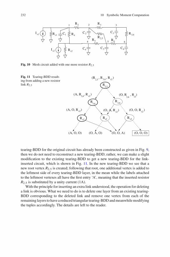
232 10 Symbolic Moment Computation
5
3
C2 C3 R3,6
R2
I s1 R4
C6C5C4I s2 Rs2
R6
C1
R5
R2,5
1 2 3
Rs1
4 6
R
Fig. 10 Mesh circuit added with one more resistor R2,5
Fig. 11 Tearing-BDD result-ing from adding a new resistorlink R2,5
Rs2
R3,6
(O, A, R )s2
(A, O, R )s2
2,5(R , R , R )
s23,6
R2,5
R3,6
Rs2Rs2
(O, O, R )s2
(A, R , R )s23,6
(A, O, O) (O, A, O) (O, O, A) (O, O, O)
(O, R , R )s23,6
tearing-BDD for the original circuit has already been constructed as given in Fig. 9,then we do not need to reconstruct a new tearing-BDD; rather, we can make a slightmodification to the existing tearing-BDD to get a new tearing-BDD for the link-inserted circuit, which is shown in Fig. 11. In the new tearing-BDD we see that anew root vertex R2,5 is created; following that root, one additional vertex is added tothe leftmost side of every tearing-BDD layer, in the mean while the labels attachedto the leftmost vertexes all have the first entry ‘A’, meaning that the inserted resistorR2,5 is substituted by a unity current (1A).
With the principle for inserting an extra link understood, the operation for deletinga link is obvious. What we need to do is to delete one layer from an existing tearing-BDD corresponding to the deleted link and remove one vertex from each of theremaining layers to have a reduced triangular tearing-BDD and meanwhile modifyingthe tuples accordingly. The details are left to the reader.

3 Mesh Circuits with Multiple Sources 233
3.6 Algorithm Complexity
Because of the regular structure created for SMC, the complexity estimation is easy.For a mesh circuit with K resistor links (including the grounding links), the totalnumber of vertices to be constructed in a tearing-BDD is
∑K+1t=1 t = 1
2 (K +1)(K +2),which grows quadratically in K . When computing the 0th order moments, all nodalvoltages of the network must be updated once at each tearing-BDD vertex using theformula (17). Suppose the mesh has N nodes and the maximum number of linksdoes not exceed N . Then the total computational cost for computing the 0th ordermoments of such a mesh circuit is of the polynomial complexity O(N3). For higher-order moments, this complexity is lower because only K tearing-BDD vertices haveto be updated once each round, as we said before.
4 Symbolic Moment Sensitivity
Symbolic moment is different from numerically computed moment in that a regulardata structure is constructed and preserved in the computer memory throughout theruntime of the program. The maintenance of a static computational data structure isbeneficial to those design automation tasks that require repeated numerical evalua-tions or analytical deductions such as sensitivity analysis. In this section we studyhow the sensitivity can be computed on a structural SMC.
In interconnect analysis, we might need to analyze timing or crosstalk measuresand their dependence on the geometrical dimensions of an interconnect network.Sensitivity is a good measure for the dependence. Sensitivity analysis in numericalsimulators mainly uses fairly standard methods such as adjoint network [268] whosecomputation requires solving the whole network as a single set of equations. In thescenario of repeated computations, say, for synthesizing an interconnect network[156], the computational efficiency of numerical sensitivity is a concern. Repeatedsensitivity computation is also demanded in statistical validation of interconnectswith the current variation-severe process technology.
With analytical representation of moments by an SMC, the sensitivity of momentwith respect to selected parameters can be calculated by pre-coded data structure thatimplements the chain rule for differentiation. Because SMC is created in the formof a recursive data structure, implementation of chain rule is fairly straightforwardand memory can easily be managed by extending the already existing SMC vertexesto incorporate intermediately computed gradient information. Therefore, it is unnec-essary to employ other advanced computational tools like automatic differentiation(AD) [142], which relies on automatic code generation, but a user is less able tointerfere.
Let us first define the gradient vectors for a moment mi,k , which is the kth ordermoment at network node i. The gradient vectors of moment with respect to a set ofselected resistors or capacitors are written by
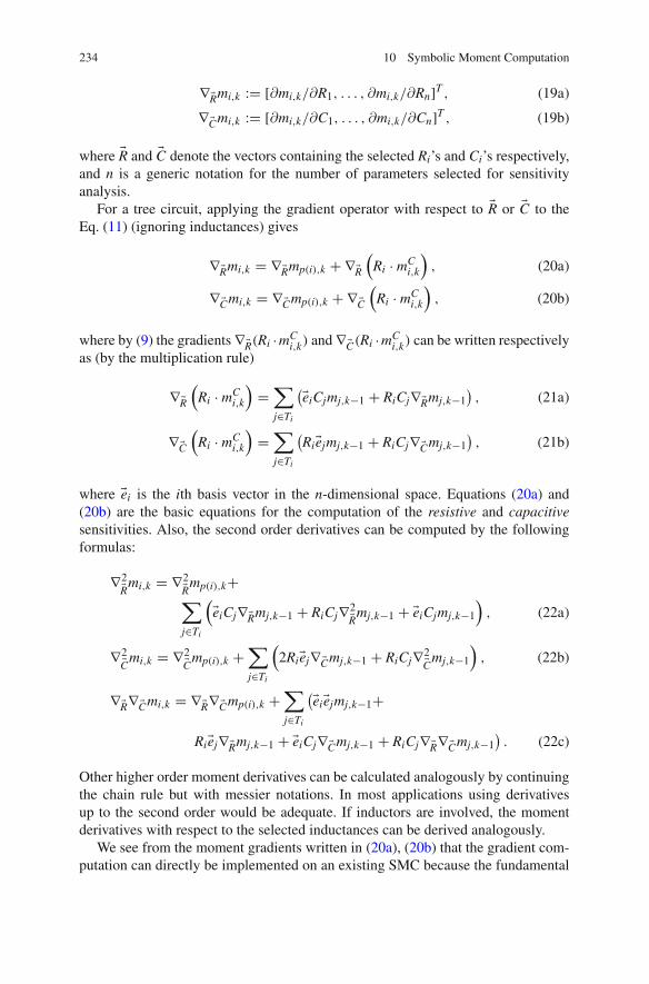
234 10 Symbolic Moment Computation
⊕∗Rmi,k := [∂mi,k/∂R1, . . . , ∂mi,k/∂Rn]T , (19a)
⊕∗Cmi,k := [∂mi,k/∂C1, . . . , ∂mi,k/∂Cn]T , (19b)
where ∗R and ∗C denote the vectors containing the selected Ri’s and Ci’s respectively,and n is a generic notation for the number of parameters selected for sensitivityanalysis.
For a tree circuit, applying the gradient operator with respect to ∗R or ∗C to theEq. (11) (ignoring inductances) gives
⊕∗Rmi,k = ⊕∗Rmp(i),k + ⊕∗R(
Ri · mCi,k
⎡, (20a)
⊕∗Cmi,k = ⊕∗Cmp(i),k + ⊕∗C(
Ri · mCi,k
⎡, (20b)
where by (9) the gradients ⊕∗R(Ri ·mCi,k) and ⊕∗C(Ri ·mC
i,k) can be written respectivelyas (by the multiplication rule)
⊕∗R(
Ri · mCi,k
⎡=
⎢
j≤Ti
(∗eiCjmj,k−1 + RiCj⊕∗Rmj,k−1), (21a)
⊕∗C(
Ri · mCi,k
⎡=
⎢
j≤Ti
(Ri∗ejmj,k−1 + RiCj⊕∗Cmj,k−1
), (21b)
where ∗ei is the ith basis vector in the n-dimensional space. Equations (20a) and(20b) are the basic equations for the computation of the resistive and capacitivesensitivities. Also, the second order derivatives can be computed by the followingformulas:
⊕2∗Rmi,k = ⊕2
∗Rmp(i),k+⎢
j≤Ti
(∗eiCj⊕∗Rmj,k−1 + RiCj⊕2
∗Rmj,k−1 + ∗eiCjmj,k−1
⎡, (22a)
⊕2∗Cmi,k = ⊕2
∗Cmp(i),k +⎢
j≤Ti
(2Ri∗ej⊕∗Cmj,k−1 + RiCj⊕2
∗Cmj,k−1
⎡, (22b)
⊕∗R⊕∗Cmi,k = ⊕∗R⊕∗Cmp(i),k +⎢
j≤Ti
(∗ei∗ejmj,k−1+
Ri∗ej⊕∗Rmj,k−1 + ∗eiCj⊕∗Cmj,k−1 + RiCj⊕∗R⊕∗Cmj,k−1). (22c)
Other higher order moment derivatives can be calculated analogously by continuingthe chain rule but with messier notations. In most applications using derivativesup to the second order would be adequate. If inductors are involved, the momentderivatives with respect to the selected inductances can be derived analogously.
We see from the moment gradients written in (20a), (20b) that the gradient com-putation can directly be implemented on an existing SMC because the fundamental

4 Symbolic Moment Sensitivity 235
sequence of computation is not altered at all, except for allocating extra memoryspace for saving the intermediate gradient vectors. The computation of the gradientvectors still obey the bottom-up propagation within the SMC data structure, as seenfrom the equations in (20a), (20b).
For a mesh circuit with resistor links, the gradient vector computation has to takeinto account of the superposition defined by (18b) for each tearing-BDD vertexes(see Fig. 9). Taking gradient operation of (18b) leads to (again by the multiplicationrule)
⊕ξmi,k = ⊕ξm(O)i,k − ⊕ξIR,k · m(A)
i,k − IR,k · ⊕ξm(A)i,k , (23)
where ξ is any parameter selected for sensitivity. Since IR,k in the above expressionis given by
IR,k = m(O)p,k − m(O)
q,k
Rlink +(
m(A)p − m(A)
q
⎡ , (24)
⊕ξIR,k can be computed in terms of ⊕ξm(O)i,k and ⊕ξm(A)
i , which are already computedand saved in their corresponding tearing-BDD vertices.
As far as the computational complexity of sensitivity is concerned, we observethat there is no substantial complexity increase except for extra memory required forthe intermediate gradient vectors saved with the SMC vertices. The total amount ofcomputation required for the gradient vectors increases proportionally to the numberof sensitivity parameters selected and the number of SMC vertices created.
By the way we point out that one more important advantage of the SMC-basedsymbolic sensitivity method is that the moment sensitivity can be computed simul-taneously with the moments in the course of traversing an SMC bottom-up.
5 SMC Efficiency
SMC is a compact data structure in that it is constructed once but can be usedrepeatedly. Although the construction time could be high for large-scale mesh circuitswith a great number of resistor links, the computation speed is fast because redundantcomputations are avoided due to sharing. An extensive efficiency evaluation of SMChas been presented in [77], from which we cite a few results to demonstrate theefficiency.
An SMC is a hierarchically linked data structure composed by several components,including a C-tree consisting of capacitor nodes, a spanning tree consisting of R(L)-nodes, and a tearing-BDD consisting of the R-vertexes representing the torn R-links.All nodes in the data structure have direct correspondence to the network elements.Therefore, whenever the network elements change values, the SMC node values canbe updated directly and another execution of the SMC recomputes all moments andsensitivity.
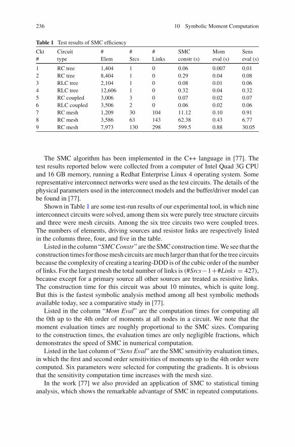
236 10 Symbolic Moment Computation
Table 1 Test results of SMC efficiency
Ckt Circuit # # # SMC Mom Sens# type Elem Srcs Links constr (s) eval (s) eval (s)
1 RC tree 1,404 1 0 0.06 0.007 0.012 RC tree 8,404 1 0 0.29 0.04 0.083 RLC tree 2,104 1 0 0.08 0.01 0.064 RLC tree 12,606 1 0 0.32 0.04 0.325 RC coupled 3,006 3 0 0.07 0.02 0.076 RLC coupled 3,506 2 0 0.06 0.02 0.067 RC mesh 1,209 30 104 11.12 0.10 0.918 RC mesh 3,586 63 143 62.38 0.43 6.779 RC mesh 7,973 130 298 599.5 0.88 30.05
The SMC algorithm has been implemented in the C++ language in [77]. Thetest results reported below were collected from a computer of Intel Quad 3G CPUand 16 GB memory, running a Redhat Enterprise Linux 4 operating system. Somerepresentative interconnect networks were used as the test circuits. The details of thephysical parameters used in the interconnect models and the buffer/driver model canbe found in [77].
Shown in Table 1 are some test-run results of our experimental tool, in which nineinterconnect circuits were solved, among them six were purely tree structure circuitsand three were mesh circuits. Among the six tree circuits two were coupled trees.The numbers of elements, driving sources and resistor links are respectively listedin the columns three, four, and five in the table.
Listed in the column “SMC Constr” are the SMC construction time. We see that theconstruction times for those mesh circuits are much larger than that for the tree circuitsbecause the complexity of creating a tearing-DDD is of the cubic order of the numberof links. For the largest mesh the total number of links is (#Srcs−1+#Links = 427),because except for a primary source all other sources are treated as resistive links.The construction time for this circuit was about 10 minutes, which is quite long.But this is the fastest symbolic analysis method among all best symbolic methodsavailable today, see a comparative study in [77].
Listed in the column “Mom Eval” are the computation times for computing allthe 0th up to the 4th order of moments at all nodes in a circuit. We note that themoment evaluation times are roughly proportional to the SMC sizes. Comparingto the construction times, the evaluation times are only negligible fractions, whichdemonstrates the speed of SMC in numerical computation.
Listed in the last column of “Sens Eval” are the SMC sensitivity evaluation times,in which the first and second order sensitivities of moments up to the 4th order werecomputed. Six parameters were selected for computing the gradients. It is obviousthat the sensitivity computation time increases with the mesh size.
In the work [77] we also provided an application of SMC to statistical timinganalysis, which shows the remarkable advantage of SMC in repeated computations.

5 SMC Efficiency 237
Also, it was shown that using some approximate metrics in terms of several low-ordermoments could capture some commonly used measures for timing and signalintegrity in a statistical setting while sacrificing only minor accuracy.
6 Summary
Symbolic moment computation is an alternative approach to Symbolic Model OrderReduction proposed in [205] for parametric modeling of high-dimensional circuitssubject to significant parameter variations. So far, except for some special structurecircuits, SMOR for general circuits is an unsolved problem. The SMC techniquedeveloped in this chapter has extended the category of circuits that can be analyzedby a parametric approach. Although we do not directly create parametric models,practice has shown that the moments computed by SMC, if used properly, can addressmost of the analysis and synthesis problems arising from interconnect networkssubject to large variations.
Finally, we stress that the idea of incremental analysis developed from the perspec-tive of circuit tearing is a generic methodology for symbolic circuit analysis. Com-plicated matrix solving involved with the moment computations have been replacedby a convenient data structure construction. This idea is believed to be a fundamentalprinciple that can be applied to other formulations of symbolic analysis problems.

Chapter 11Performance Bound Analysis of AnalogCircuits Considering Process Variations
1 Introduction
It is well accepted that variations have huge impacts on circuit performance, yield,and reliability in the nanometer regime. Analog and mixed-signal circuits are espe-cially sensitive to process variations as a lot of matching and regularities are required.This situation becomes worse as technology continues to scale down to 45 nm andbelow owing to the increasing process-induced variability [141, 170]. Transistor-level mismatch is the primary obstacle to reach a high yield rate for analog designsin deep submicron technologies. For example, due to an inverse-square-root-lawdependence with the transistor area, the mismatch of CMOS devices nearly dou-bles for each process generation less than 90 nm [95, 128]. Since the traditionalworst-case or corner-case based analysis is either so pessimistic that it sacrificesspeed, power, and area, or too expensive for practical full-chip design, statisticalapproaches thereby become imperative to estimate the analog mismatch and per-formance variations [149]. The variations in the analog components can come fromsystematic (or global spatial variation) ones and stochastic (or local random varia-tion) ones. In this chapter, we model both variations as parameter intervals on thecomponents of analog circuits.
Analog circuit designers usually perform a Monte-Carlo (MC) analysis to ana-lyze the stochastic mismatch and predict the variational responses of their designsunder faults. However, MC method is expensive and slow especially for rare events(high sigma estimations) as more samplings are required, which will lead to thebottleneck of analog circuit optimization. Many fast Monte Carlo methods havebeen proposed to improve the efficiency of classical Monte Carlo methods. Exist-ing approaches include importance sampling [40], Latin hypercube sampling basedmethod [146, 225], and quasi Monte Carlo based method [120, 209]. However,the importance sampling method is circuit specific, Latin hypercube sampling doesnot work for all the circuits, and quasi Monte Carlo method suffers the high-dimensional problems [146]. We remark that MC and its variants still remain the
G. Shi et al., Advanced Symbolic Analysis for VLSI Systems, 239DOI: 10.1007/978-1-4939-1103-5_11,© Springer Science+Business Media New York 2014
240 11 Performance Bound Analysis of Analog Circuits Considering Process Variations
popular approaches for statistical analysis and optimization for [wdanalog/mixed-signal methods at current stage. But more efficient variational analysis techniques,especially non-MC methods, are still highly desirable.
Bound analysis or worst case analysis of analog circuits under parameter varia-tions has been studied in the past for fault-driven testing and tolerance analysis ofanalog circuits [97, 198, 239]. Among them, sensitivity analysis [252], samplingmethod [218], and interval arithmetic based approaches [97, 198, 239] have theiradvantages in well suited scenarios. However, sensitivity based methods cannot givethe worst case in general, sampling based methods are limited to a few number ofvariables, and interval arithmetic methods have the notoriety of overly pessimism.Recently, worst-case analysis of linearized analog circuits in frequency domain hasbeen proposed [158], where Kharitonov’s functions [93] were applied to obtain theperformance bounds in frequency domain, but no systematic method was proposed toobtain variational transfer functions. This was later improved by [78], where symbolicanalysis approach was applied to derive exact transfer functions and affine intervalmethod was used to compute variational transfer functions. However, the affine inter-val method can lead to over-conservative results. Recently, authors in [177] appliedan optimization based method to compute the bounds. Another recent work [217],using reachability analysis, can also efficiently generate the variation induced per-formance bounds. But still, no systematic method was proposed to obtain variationalperformance objective functions from the circuit netlist.
In this chapter, we present several new performance bound analysis of analog cir-cuits considering process variations. The first presented works are based on recentlyworks, which are based on the optimization methods to find the bounds in thefrequency domains [121, 122] and recently in the time domain directly [275].
The first method employs several techniques to compute the response bounds ofanalog circuits in both frequency domain and time domain. The overall algorithmconsists of several steps. First, the new method models the variations of componentvalues as intervals measured from tested chips and manufacture processes. Then,determinant decision diagram (DDD) graph-based symbolic analysis is applied toderive the exact symbolic transfer functions from linearized analog circuits. Afterthis, we formulate the bound problem into nonlinear constrained optimization prob-lem, where the objective functions are the magnitudes or phases of the transferfunctions, subject to linear constraints, which are the ranges of process variationalparameters. The nonlinear constrained optimization problems are then solved bythe active-set algorithm, a general nonlinear optimization method. The optimizationis solved on each frequency point of interest. The maximum and minimum valuereturned by the optimization solver will compose lower and upper bounds of thefrequency domain response. One important feature of the presented method is thatthe bounds computed in this way are very accurate and have no over-conservativeness,which are suffered by some existing approaches such as interval arithmetic or affinearithmetic based methods. As an application of our frequency domain bound analysis,we also show results of analog circuit yield calculation in the experiment section.
To compute the time domain bound, we present a generalized time domain boundanalysis technique, or TIDBA, in which time domain response bounds of circuits

1 Introduction 241
with general input signals can be computed based on the given frequency domainresponses. This represents a major improvement over the existing method [155].Experimental results from several analog benchmark circuits show that TIDBA givesthe correct time domain bounds verified by MC analysis, while it delivers one orderof magnitude speedup over MC.
The second method directly obtains the performance bounds in the time domain,which overcomes the problems in the first method [275]. Specifically, we present ageneral time-domain performance analysis method, which consists of several steps:First the time-domain symbolic modified nodal analysis (MNA) formulation of (lin-earized) analog and interconnect circuits at a time step is formed. Then the closed-form expressions of the interested performance in terms of variational parameters ofthe circuit matrices of (linearized) analog and interconnect circuits are derived viaa graph-based symbolic analysis method. Then time-domain performance responsebounds of current time step are obtained by finding the max/min values via a nonlinearconstrained optimization process subject to the parameter variations and variationalcircuit state bounds computed from the previous time step.
In this chapter, we also further study the bounds computed by the presented methodagainst the different sigma bounds by the standard MC method, which shows thatthe method is more efficient for computing high sigma bounds than the MC method,which will increase rapidly (almost exponentially) with increasing sigma. In contrast,the run time of the method will remain the almost the same as it only deals withdifferent parameter bounds with the same number of parameters.
Experimental results show that the new method can delivers one or two order ofmagnitudes speedup over standard Monte Carlo simulation on some typical analogcircuits and interconnect circuits with very high accuracy.
The rest of this chapter is organized as follows. Section 2 gives a review on deter-minant decision diagram based symbolic generation of transfer functions. We presentthe frequency domain performance bound analysis using nonlinear constrained opti-mization in Sect. 3. Then Sect. 4 introduces time domain bound analysis TIDBA.Section 6 shows the experimental results. Finally, Sect. 7 summarize this chapter.
2 Variational Transfer Functions Based on DDDs
In this section, we first show the concept of variational transfer functions based onthe determinant decision diagram (DDD) [196] concept discussed in the Chap. 3.
2.1 Variational Transfer Functions Due to Process Variations
In order to compute the symbolic coefficients of the transfer function in differ-ent powers of frequency s, the original DDD can be expanded to the s-expandedDDD [197]. Specifically, to obtain the transfer function H(s), we can build the s-

242 11 Performance Bound Analysis of Analog Circuits Considering Process Variations
NoratorNullator
N
G+
−
vD
D
Sis gcur
Fig. 1 The small-signal model for MOS transistors (left) and a simple circuit example (right)
expanded DDD [197] as follows:
H(s, p1, . . . , pm) =∑m
i=0 ai(p1, . . . , pm)si∑n
j=0 bj(p1, . . . , pm)sj, (1)
where coefficients ai(p1, . . . , pm) and bj(p1, . . . , pm) are presented by each rootin s-expanded DDD graphs, and p1, . . . , pm are m circuit variables. Notice thatH(s, p1, . . . , pm) is a nonlinear function of pi, i = 1, . . . , m.
In this book, we assume that each circuit parameter pi is a random variable witha variational range. We assume that the device level variations in terms of electri-cal parameters such as transconductances gm and gds (shown in Fig. 1) will be firstobtained by device characterization using data from the foundry. Let s = jα. The eval-uation of the transfer function gives a complex valued result, H(jα) = H0(α)ejβ(α),where the magnitude H0(α) = |H(jα)| and the phase angle β(α) = ∠H(jα) are realvalues. In variation analysis, instead of getting a nominal transfer function, we willobtain a variational transfer function with bounded magnitude and phase regions,i.e.,
H0l (α) ≤ H0(α) ≤ H0
u (α), (2)
βl(α) ≤ β(α) ≤ βu(α), (3)
where H0l (α) and H0
u (α) are the lower and upper bounds of magnitude, and βl(α)
and βu(α) are the lower and upper bounds of phase.
3 Computation of Frequency Domain Bounds
In this section, we first describe the performance bounds in frequency domain for acircuit under process variation. Then, to compute the bounds, we present the opti-mization based method, which is very general and accurate.
We start with a specific example to look at the frequency domain bound problem.The example is a simplified MOS device model as shown in the left part of Fig. 1, in

3 Computation of Frequency Domain Bounds 243
45
6 x 10⁻³
11.2x 10
−4
92
93
94
95
gmgds
Gai
n (d
B)
45
6 x 10⁻³
11.2x 10
−4
81
81.5
82
gmgds
Gai
n (d
B)
45
6 x 10⁻³
11.2x 10
−4
42
43
44
45
gmgds
Gai
n (d
B)
10−2
100
102
104
106
108
1010
30
40
50
60
70
80
90
freq (Hz)
Gai
n (d
B)
f = 1× 10⁸ Hzf = 1× 10⁵ Hzf = 1× 10³ Hz
Fig. 2 Frequency response of the simplified MOS model driven by Norton current source. Solidcurve is the magnitude response with nominal parameters, while the two dashed curves are lowerand upper bounds due to process variation. The three surfaces on top, with gds and gm as x-axis andy-axis accordingly, and magnitude as z-axis, illustrate the variations of magnitude at three samplingfrequencies
which the singular network elements like nullator and norators are used to model theideal voltage controlled current sources (VCCS). Suppose we apply a Norton currentsource, i.e, an ideal current source is with a parallel resistor gcur, shown in the rightpart of Fig. 1, onto the gate node G of the MOS model, the exact symbolic transferfunction from is to the observed voltage on drain node D can be obtained as
H(jα) = vD(jα)
is(jα)= gm − jαCgd
(jα)2CgsCgd + jα(Cgsgds + Cgd(gds + gm + gcur)) + gdsgcur.
(4)
Once the exact transfer function and variations of the parameters such as gm, gds,Cgd, and Cgs are known, one can find the bounds of H(jα). The variational bounds ofthe transfer function are plotted in Fig. 2 where we have two variational parametersgds and gm. The variation spaces for the two variables at three different frequenciesare also shown on the top of the figure, which show the searching spaces at thosefrequency for the two variables. Here, we adopt the term “searching spaces” frommathematical programming and optimization, which is used in the presented methodand will be talked about later.
To obtain the performance bounds of analog circuits in frequency domain, the firststep is to obtain the exact symbolic transfer functions like Eq. (4) in terms of all thevariational circuit parameters. This will be done by the DDD-based exact symbolic

244 11 Performance Bound Analysis of Analog Circuits Considering Process Variations
analysis as mentioned in Sect. 2. We remark that one can also use circuit simulatorlike SPICE to evaluate the performances for a given set of parameter values andfrequency points. But the DDD method is relevant here because it can give closedform expressions for a given circuit performance, which can lead to much fasterevaluations compared to numerical methods [196].
Secondly, after the exact symbolic transfer functions are available, we need to finda systematic way to obtain the performance bounds given the bounds of variationalparameters. In this work, we formulate the bound computing problem into a nonlinearconstrained optimization problem. To obtain the performance bounds for magnitudeand phase at one frequency point, four evaluation processes, or optimization runs,of the transfer function are needed: min/max optimizations for H0(α), and min/maxoptimizations for β(α). The range of frequency sweep and number of frequencypoints are determined freely by the designer. We use the lower bound of the magnituderesponse H0(α) frequency α for an example. The magnitude of the transfer function,which can be evaluated from the available symbolic transfer function, is used as thenonlinear objective function to be minimized:
minimize H0(α, x)
subject to xlower ≤ x ≤ xupper,(5)
where x = [p1, . . . , pm] represents the circuit parameter variable vector, which issubject to the optimization constraints xlower ≤ x ≤ xupper. In circuit design, theseconstraints are supplied by foundries and cell library vendors. Hence, after (5) issolved by an optimization engine, the lower bound of the magnitude response at α,i.e., H0
l (α), is returned and a parameter set x∈ at which the minimum is attained willalso be saved as a by-product.
We remark that the worst cases of magnitude may not be the worst cases of phaseand the two worst case performance metrics do not have specific correlations. Afterwe calculate the worst case for the performances of interests, such as magnitude orphase, at every frequency point, we can obtain the worst case curves (upper or lowerbounds) in the frequency domain as shown in Fig. 2.
The nonlinear optimization problem with simple upper and lower bounds givenin (5) can be efficiently solved by several methods such as active-set, interiorpoint, and trust region algorithms [18, 53, 63]. All those methods are iterativeapproaches starting with an initial feasible solution. In this work, we use the active-set method [53], as it turns to be the most robust nonlinear optimization method forour application. Active-set methods are two-phase iterative methods that provide anestimate of the active set (active set is the set of constraints that are satisfied withequality) at the solution. In the first phase, the objective is ignored while a feasiblepoint x0 is found for the constraints. In the second phase, the objective is minimizedwhile feasibility is maintained. Starting from the feasible x0, the second phase com-putes a sequence of feasible solutions {xk} such that xk+1 = xk + τkpk , where pkis a nonzero search direction and τk is a non-negative step length. Hence, the newsolution xk+1 makes the cost function or objective function smaller than its precedentxk does. Methods like quadratic programming can be used in this phase.

3 Computation of Frequency Domain Bounds 245
Fig. 3 The flowchart offrequency domain perfor-mance bound calculation
Symbolic analysis
Constrained Optimizations
Range of VariationalParameters
Circuit Netlist
for Transistors
Transfer Function
Magnitude and PhaseMin and Max of
Linear Model
Algorithm 1 Calculation of frequency response bounds via symbolic analysis andnonlinear constrained optimization.1: Read circuit netlist.2: Set bounds on process variation affected parameters.3: Generate symbolic expression of transfer functions.4: for each frequency αi do5: Nonlinear constrained optimization (5) which uses transfer function as objective to find mag-
nitude and phase bounds on αi.6: Save bound information for future statistical and yield analysis.
To further speed up the optimization, the initial point selection can be furtherimproved. Since the responses at two neighboring frequency points are usually closeto each other, the starting point x for frequency point αi+1 can be set using thesolution at the previous frequency point αi. Therefore, the initial guess point doesnot always have to be the nominal value set, and the previous frequency’s optimalpoint is heuristically the best shortcut of initial guess at current frequency. Thisstrategy tends to reduce the time required by the optimization to search its minimalor maximal point in the whole variation space, and thus speed up the calculationtime of the bound analysis. Fig. 3 summarizes the flow of the performance boundcalculation.
We remark that the active-set method is still a local optimization method, whichfinds the local optimum. It will be desirable to find the global optimum, which cangive true “confident” bounds of performance. But this goal may come with moreor much higher computing costs by performing many tries. The effort boils downto a trade-off between accuracy and costs in this problem. In our approach, westill perform one optimization. Our numerical results show that by using reasonableinitial guesses as mentioned before, the presented method gives very close boundscompared with MC methods for the examples being used.

246 11 Performance Bound Analysis of Analog Circuits Considering Process Variations
4 Time Domain Bound Analysis Method
In the previous section, we have shown our frequency domain performance boundmethod using symbolic analysis and constrained optimization. Based on the calcu-lated frequency domain bounds, we next develop our time domain bound analysis,or TIDBA, which converts the frequency domain bounds to time domain bounds forgeneral input signals. TIDBA is inspired by [155], which determines time domainperformance bounds of an uncertain system for impulse or step input signals. How-ever, this method does not give transient performance bounds in response to generalinput signals, which are required by analog circuit analysis. Note that the bounds ofmagnitude and phase of the transfer function required by TIDBA can be generatedby any existing bound analysis methods and not limited to the one we presented inthe previous section.
We first present the whole TIDBA flow in Algorithm 2. As can be seen from theflow, the time domain bound analysis requires the results such as transfer functionbounds from the procedures we studied in previous sections. After the first two steps,the bounds of magnitude and phase (angle) shown in the inequalities (2) and (3) areavailable. Then TIDBA converts frequency domain performance bounds into the timedomain performance bounds by impulse signal based time domain bound analysisand FFT/IFFT, which will be the focus of this section.
Algorithm 2 The algorithm flow of the new time domain performance boundanalysis—TIDBA.Require: circuit netlist with variational parameters; stimulus signal of the circuit.Ensure: lower and upper bounds of the output signal in time domain.1: Generate symbolic expression of circuit transfer function by graph-based symbolic method.
Variational parameters are represented as symbols.2: Compute the performance bounds of the variational transfer function by nonlinear constrained
optimization.3: Compute time domain performance bounds by our new general-signal transient bound analysis
presented in Sect. 4.2.
4.1 Review of Transient Bound Analysis Driven by Impulse Signals
For the completeness of our presentation, we briefly review the work in [155] whichprovides transient bound analysis with impulse input signals.
For a purely real signal x(t) in time domain, its Fourier transform X(jα) = X0(α)·ejπ(α) in frequency domain holds the property of conjugate symmetry, i.e.,
X(−jα) = X(jα)∈. (6)
It can be equivalently expressed by the even property of magnitude and the oddproperty of phase: X0(−α) = X0(α), and π(−α) = −π(α). It is not difficult

4 Time Domain Bound Analysis Method 247
to show that the transfer function of a physically realizable system also holds theconjugate symmetry property [101].
Since the spectrum of an impulse signal δ(t) is X(jα) = 1 everywhere on allfrequencies, the spectrum of the system’s output signal is Y(jα) = X(jα)H(jα) =H(jα), and hence the impulse response of the system in time domain is simply theinverse Fourier transform of H(jα),
y(t) = 1
2π
∧⎡
−∧H(jα)ejαtdα
= 1
2π
∧⎡
−∧H0(α)ej(αt+β(α))dα, t > 0. (7)
Employing the even and odd properties of H(jα), Eq. (7) can be equivalently inte-grated from α = 0 to ∧,
y(t) = 1
π
∧⎡
0
H0(α)(ej(αt+β(α)))dα
= 1
π
∧⎡
0
H0(α) cos(αt + β(α))dα, t > 0. (8)
A modification of this integral to discrete sum on sampled frequency points allowsone to calculate the approximate result of y(t) at each time point as
y(t) = 1
π
N−1⎢
n=0
H0(αn) cos(αnt + β(αn))⎣ ⎤⎥ ⎦I(αn)
�αn, t > 0. (9)
In the presence of process variation, the transfer function will be given in the boundedform in (2) and (3). Therefore, to compute the lower and upper transient bounds yl(t)and yu(t) for each time point t, the integrand body I(αn) in Eq. (9) is calculated usingthe following rules.
First, find the minimum and maximum values of cos(αnt+β(αn)), where the phaseangle β(αn) can vary in the interval [βl(αn), βu(αn)]. Let Cmin(αn) and Cmax(αn)
denote the two extreme values of the cosine function. Then, for yl(t), all I(αn) shallbe calculated as
I(αn) ={
H0u (αn)Cmin(αn), Cmin(αn) ≤ 0
H0l (αn)Cmin(αn), Cmin(αn) > 0,
(10)

248 11 Performance Bound Analysis of Analog Circuits Considering Process Variations
and, for yu(t), the situation is simply reversed,
I(αn) ={
H0l (αn)Cmax(αn), Cmax(αn) ≤ 0
H0u (αn)Cmax(αn), Cmax(αn) > 0.
(11)
4.2 The General Signal Transient Bound Analysis Method
For a general time domain signal x(t) in circuit analysis application, its frequency-domain transform X(jα) can be calculated by fast Fourier transform, FFT. Thisrequires sampling points of the signal on a set of discretized time points. For example,with a uniform sampling period Ts = 1/Fs, x(t) is sampled and stored as x(0), x(Ts),x(2Ts),…, x(NTs). For the sake of simplicity, we will omit the term Ts and denote thetime point indices by subscripts in the remainder of this chapter. Thus the notationxn will stand for the sampled value of signal x(t) at time t = nTs.
To achieve accurate results from FFT and IFFT, Nyquist sampling theoremrequires the sampling frequency Fs = 1/Ts to be at least twice of the bandwidthof signal [145]. Meanwhile, the total sampling duration T0 = TsN determines theresolution of the FFT spectrum, i.e., the sampling interval of frequency domain isF0 = 1/T0. The longer T0 is, the higher spectral resolution we can get, and thus themore sampling points are needed.
Given N sampling points, the FFT transform pair is
Xk =N−1⎢
n=0
xne−j 2πN nk, k = 0, 1, . . . , N − 1, and (12)
xn = 1
N
N−1⎢
k=0
Xkej 2πN nk, n = 0, 1, . . . , N − 1. (13)
In transient circuit analysis, the input data xn are purely real, and the symmetryproperty in Eq. 6 still holds, though in a different form, XN−k = X∈
k . This means thatthe right half spectrum Xk is a conjugate swap of its left half, except for X0, which isthe zero-frequency or “DC” component of the spectrum. The points in the left half,i.e., Xk for k = 0, . . . , N/2, are the spectral points of frequencies f = kF0. Fig. 4illustrates the FFT series and its conjugate symmetry property.
Based on this property of a real signal’s spectrum, the inverse discrete Fouriertransform can be calculated with the spectrum’s left half. Consequently, the equiva-lent form of Eq. (13) becomes
xn = 1
N
⎛X0 + 2N/2⎢
k=1
(Xkej 2πN nk)
⎧
⎪ , n = 0, 1, . . . , N − 1. (14)
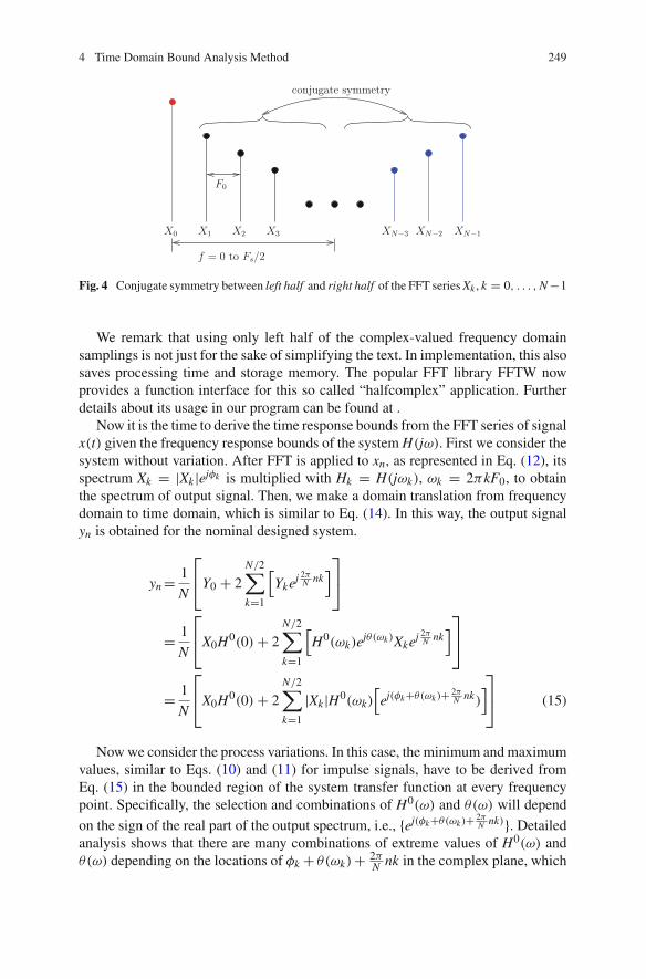
4 Time Domain Bound Analysis Method 249
f = 0 to Fs/2
X0 X1 X2 X3 XN−3 XN−2 XN−1
F0
conjugate symmetry
Fig. 4 Conjugate symmetry between left half and right half of the FFT series Xk , k = 0, . . . , N −1
We remark that using only left half of the complex-valued frequency domainsamplings is not just for the sake of simplifying the text. In implementation, this alsosaves processing time and storage memory. The popular FFT library FFTW nowprovides a function interface for this so called “halfcomplex” application. Furtherdetails about its usage in our program can be found at .
Now it is the time to derive the time response bounds from the FFT series of signalx(t) given the frequency response bounds of the system H(jα). First we consider thesystem without variation. After FFT is applied to xn, as represented in Eq. (12), itsspectrum Xk = |Xk |ejπk is multiplied with Hk = H(jαk), αk = 2πkF0, to obtainthe spectrum of output signal. Then, we make a domain translation from frequencydomain to time domain, which is similar to Eq. (14). In this way, the output signalyn is obtained for the nominal designed system.
yn = 1
N
⎛Y0 + 2N/2⎢
k=1
⎨Ykej 2π
N nk⎩⎧
⎪
= 1
N
⎛X0H0(0) + 2N/2⎢
k=1
⎨H0(αk)e
jβ(αk)Xkej 2πN nk
⎩⎧
⎪
= 1
N
⎛X0H0(0) + 2N/2⎢
k=1
|Xk|H0(αk)⎨ej(πk+β(αk)+ 2π
N nk)⎩⎧
⎪ (15)
Now we consider the process variations. In this case, the minimum and maximumvalues, similar to Eqs. (10) and (11) for impulse signals, have to be derived fromEq. (15) in the bounded region of the system transfer function at every frequencypoint. Specifically, the selection and combinations of H0(α) and β(α) will depend
on the sign of the real part of the output spectrum, i.e., {ej(πk+β(αk)+ 2πN nk)}. Detailed
analysis shows that there are many combinations of extreme values of H0(α) andβ(α) depending on the locations of πk + β(αk) + 2π
N nk in the complex plane, which
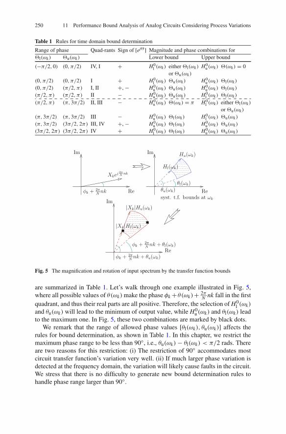
250 11 Performance Bound Analysis of Analog Circuits Considering Process Variations
Table 1 Rules for time domain bound determination
Range of phase Quad-rants Sign of [ej] Magnitude and phase combinations forl(αk) u(αk) Lower bound Upper bound
(−π/2, 0) (0, π/2) IV, I + H0l (αk) either l(αk) H0
u (αk) (αk) = 0or u(αk)
(0, π/2) (0, π/2) I + H0l (αk) u(αk) H0
u (αk) l(αk)
(0, π/2) (π/2, π) I, II +, − H0u (αk) u(αk) H0
u (αk) l(αk)
(π/2, π) (π/2, π) II − H0u (αk) u(αk) H0
l (αk) l(αk)
(π/2, π) (π, 3π/2) II, III − H0u (αk) (αk) = π H0
l (αk) either l(αk)
or u(αk)
(π, 3π/2) (π, 3π/2) III − H0u (αk) l(αk) H0
l (αk) u(αk)
(π, 3π/2) (3π/2, 2π) III, IV +, − H0u (αk) l(αk) H0
u (αk) u(αk)
(3π/2, 2π) (3π/2, 2π) IV + H0l (αk) l(αk) H0
u (αk) u(αk)
syst. t.f. bounds at ωk
θl(ωk)θu(ωk)
Hl(ωk)Xke
j 2πN
nk
Hu(ωk)
φk + 2πN
nk + θu(ωk)
Reφk + 2πN
nk
φk + 2πN
nk + θl(ωk)
|Xk|Hu(ωk)
Re
Im Im
Im
Re
|Xk|Hl(ωk)
Fig. 5 The magnification and rotation of input spectrum by the transfer function bounds
are summarized in Table 1. Let’s walk through one example illustrated in Fig. 5,where all possible values of β(αk) make the phase πk + β(αk)+ 2π
N nk fall in the firstquadrant, and thus their real parts are all positive. Therefore, the selection of H0
l (αk)
and βu(αk) will lead to the minimum of output value, while H0u (αk) and βl(αk) lead
to the maximum one. In Fig. 5, these two combinations are marked by black dots.We remark that the range of allowed phase values [βl(αk), βu(αk)] affects the
rules for bound determination, as shown in Table 1. In this chapter, we restrict themaximum phase range to be less than 90⊆, i.e., βu(αk) − βl(αk) < π/2 rads. Thereare two reasons for this restriction: (i) The restriction of 90⊆ accommodates mostcircuit transfer function’s variation very well. (ii) If much larger phase variation isdetected at the frequency domain, the variation will likely cause faults in the circuit.We stress that there is no difficulty to generate new bound determination rules tohandle phase range larger than 90⊆.

4 Time Domain Bound Analysis Method 251
FFT
xn: input signal
system transfer function
XN/2 XN−1X0 X1
left half of spectrum
Xk: spectrum of input signal· · · · · ·
apply the rules forlower and upper bounds
θl(ω), θu(ω)Hl(ω), Hu(ω)
(frequency performance bounds)
Y lN/2Y l
1Y l0
Y l0 Y l
1 · · ·
· · ·
Y lN/2 · · ·
IFFT
xN−1x0 x1 · · ·
conjugate symmetryto form right half
yln: lower bound of output signal
Y lN−1
repeat the same procedureto get upper bound yu
n
· · ·yl0 yl
1 ylN−1
· · ·Y u0 Y u
1 Y uN/2
1
2
Fig. 6 The presented general-signal transient bound determination method
With this assumption, the rules for time domain bound determination aresummarized in Table 1. For brevity, let l(αk) = πk + βl(αk) + 2π
N nk, andu(αk) = πk + βu(αk) + 2π
N nk. If the range of is not covered by the enumeratedregions, a phase shift of 2π can be applied to relocate its value into the listed ranges.In addition, the “either l(αk) or u(αk)” in the first row and the fifth row in the tablemeans one of them will be selected: in the first row, the lower bound will happen atone of them which makes cos() smaller; and in the fifth row, the upper bound willtake place at the phase angle making cos() larger. Similarly, the uncertainty regiondescribed in the third row covers the first and the second quadrants, and this resultsin a evaluation of [ej] with positive or negative sign. Therefore, the lower bound ofy is reached with upper bound of magnitude and upper bound of phase angle, whichmake the value of cos(u) the largest negative number. And for the upper bound ofy is obtained in a converse way.
Fig. 6 shows the implementation flow of the presented general-signal transientbound determination method. It starts from a time domain sampling of input signalx(t) and given system transfer function bounds in frequency domain. The FFT opera-tion transforms the input signal to its spectrum and then the presented rules in Table 1are applied to determine the magnitude and phase combinations for lower and uppertime domain bounds at every frequency point in the left half of the spectrum. This
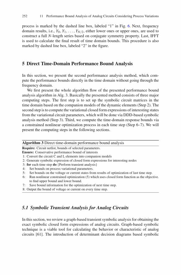
252 11 Performance Bound Analysis of Analog Circuits Considering Process Variations
process is marked by the dashed line box, labeled “1” in Fig. 6. Next, frequencydomain results, i.e., Y0, Y1, . . . , YN/2, either lower ones or upper ones, are used toconstruct a full N-length series based on conjugate symmetry property. Last, IFFTis used to calculate the final result of time domain bounds. This procedure is alsomarked by dashed line box, labeled “2” in the figure.
5 Direct Time-Domain Performance Bound Analysis
In this section, we present the second performance analysis method, which com-pute the performance bounds directly in the time domain without going through thefrequency domain.
We first present the whole algorithm flow of the presented performance boundanalysis algorithm in Alg. 3. Basically the presented method consists of three majorcomputing steps. The first step is to set up the symbolic circuit matrices in thetime domain based on the companion models of the dynamic elements (Step 2). Thesecond step is to compute the variational closed form expressions of interesting statesfrom the variational circuit parameters, which will be done via DDD-based symbolicanalysis method (Step 3). Third, we compute the time-domain response bounds viaa constrained nonlinear optimization process in each time step (Step 6–7). We willpresent the computing steps in the following sections.
Algorithm 3 Direct time-domain performance bound analysisRequire: Circuit netlist, bounds of selected parameters.Ensure: Conservative performance bound of interests1: Convert the circuit C and L elements into companion models2: Generate symbolic expression of closed form expressions for interesting nodes3: for each time step do {Perform transient analysis}4: Set bounds on process variational parameters.5: Set bounds on the voltage or current states from results of optimization of last time step.6: Run nonlinear constrained optimization (5) which uses closed form function as the objective.
to find upper bound and lower bound.7: Save bound information for the optimization of next time step.8: Output the bound of voltage or current on every time step.
5.1 Symbolic Transient Analysis for Analog Circuits
In this section, we review a graph-based transient symbolic analysis for obtaining theexact symbolic closed form expressions of analog circuits. Graph-based symbolictechnique is a viable tool for calculating the behavior or characteristic of analogcircuits [61]. The introduction of determinant decision diagrams based symbolic
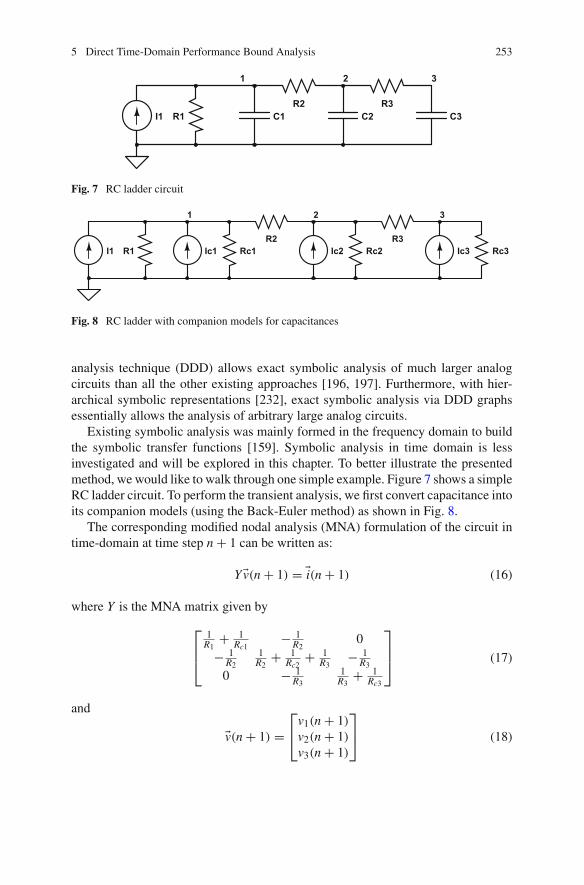
5 Direct Time-Domain Performance Bound Analysis 253
Fig. 7 RC ladder circuit
Fig. 8 RC ladder with companion models for capacitances
analysis technique (DDD) allows exact symbolic analysis of much larger analogcircuits than all the other existing approaches [196, 197]. Furthermore, with hier-archical symbolic representations [232], exact symbolic analysis via DDD graphsessentially allows the analysis of arbitrary large analog circuits.
Existing symbolic analysis was mainly formed in the frequency domain to buildthe symbolic transfer functions [159]. Symbolic analysis in time domain is lessinvestigated and will be explored in this chapter. To better illustrate the presentedmethod, we would like to walk through one simple example. Figure 7 shows a simpleRC ladder circuit. To perform the transient analysis, we first convert capacitance intoits companion models (using the Back-Euler method) as shown in Fig. 8.
The corresponding modified nodal analysis (MNA) formulation of the circuit intime-domain at time step n + 1 can be written as:
Y⊕v(n + 1) = ⊕i(n + 1) (16)
where Y is the MNA matrix given by
⎠⎛
1R1
+ 1Rc1
− 1R2
0− 1
R2
1R2
+ 1Rc2
+ 1R3
− 1R3
0 − 1R3
1R3
+ 1Rc3
⎧
⎪ (17)
and
⊕v(n + 1) =
⎛v1(n + 1)
v2(n + 1)
v3(n + 1)
⎧
⎪ (18)

254 11 Performance Bound Analysis of Analog Circuits Considering Process Variations
A B 0
C D E
0 F G
0 edge
1 0
1 edge
+
+
+
-
+
+
-
A
B
CD
F
E
G
Fig. 9 A matrix determinant and its DDD representation
and
⊕i(n + 1) =
⎛i1(n + 1) + ic1(n)
ic2(n)
ic3(n)
⎧
⎪ (19)
where Rc1 = C1�t , Rc1 = C2
�t Rc1 = C3�t , ic1(n) = v1(n)∈C1
�t , ic2(n) = v2(n)∈C2�t ,
ic3(n) = v3(n)∈C3�t and �t is the time step size.
Then the unknown nodal voltage are solved using crammer rules.
vi(n + 1) = det(Yi(n + 1))
det(Y)(20)
where Yi(n + 1) is the matrix formed by replacing the ith column of Y by vector⊕i(n + 1).
DDD is a very powerful tool to compute the symbolic determinant. Once thecharacteristics of circuits are presented by DDDs, evaluation of DDDs, whose CPUtime is proportional to the size of DDDs, will give exact numerical values.
We view each entry in the circuit matrix as one distinct symbol, and rewrite itssystem determinant in the left-hand side of Fig. 9. Then its DDD representation isshown in the right-hand side.
Once a DDD has been constructed, the numerical values of the determinant itrepresents can be computed by performing the depth-first type search of the graphand performing one multiplication and addition at each node, whose time complexityis linear function of the size of the graphs (its number of nodes). The computing step iscall Evaluate(D) where D is a DDD root. With proper node ordering and hierarchicalapproaches, DDD can be very efficient to compute transfer functions of large analogcircuits [196, 232].

5 Direct Time-Domain Performance Bound Analysis 255
5.2 Variational Symbolic Closed-Form Expressionsfor Transient States
To find the performance bounds of specific transient state variable, say vi(n + 1) attime step n + 1, DDD graphs are built for det(Yi(n + 1) and det(Y), we will obtainthe following closed form symbolic expression for vi(n + 1),
vi(n + 1) = fi(p1, . . . , pm, v1(n), . . . , vk(n))
= fn,i(p1, . . . , pm, v1(n), . . . , vk(n))
fd,i(p1, . . . , pm)(21)
where functions fn,i(p1, . . . , pm, v1(n), . . . , vk(n)) and fd,i(p1, . . . , pm) are repre-sented by DDD graphs and p1, . . . , pm are m circuit variables and v1(n), . . . , vk(n)
are the state variables computed from previous time step n. Notice that vi(n + 1) =fi(p1, . . . , pm, v1(n), . . . , vk(n)) describes nonlinear functions in terms of p1, . . . ,
pm, v1(n), . . . , vk(n). All the variables at current time step n + 1 have variationalbounds:
pil ≤ pi ≤ piu (22)
vil(n) ≤ vi(n) ≤ viu(n) (23)
Note that the variational bounds of state variable vi(n) are obtained form the previoustime step n. In our presentation, we assume that the external voltage or current sourcesdo not have variations to simplify our presentation. But this is not the limitation ofthe presented method and we can trivially add this into our method.
To compute the numerical value of vi(n+1) for given specific values of vi(n+1) =fi(p1, . . . , pm, v1(n), . . . , vk(n)), this can be done by DDD Evaluation operation,which traverses the DDD in a depth-first style and performs one multiplication andone addition at each node.
Get back to the illustrative example, for voltage at node i at time step n + 1,vi(n + 1), we have
vi(n + 1) = fi(C1, C2, C3, R1, R2, R3, v1(n), v2(n), v3(n))
5.3 Variational Bound Analysis in Time Domain
To find the performance bounds subject to the parameter variations at time stepn + 1, we formulate the bound computing problem into a nonlinear constrainedoptimization problem. We use the lower bound of the voltage of node i on time stepn + 1 for an example. The symbolic expression of the voltage of node1, which hasbeen obtained by DDD symbolic analysis, is used as the nonlinear objective function

256 11 Performance Bound Analysis of Analog Circuits Considering Process Variations
to be minimized:minimize vi(n + 1)(x) = fi(x)
subject to xlower ≤ x ≤ xupper,(24)
where x = [p, v], in which, p = [p1, . . . , pm] represents the circuit parametervariable vector, which is subjected to the optimization constraints [plower, pupper].In circuit design, foundries and cell library vendors supply these constraints. On theother hand, v = [v1(n), . . . , vk(n)] represents the nodal voltage on the last time step,which are determined by the results of optimization of the last time step. Hence,after (24) is solved by an optimization engine, the lower bound of the v1 on (n+1)thtime step is returned and then serves as constrained condition for the optimizationof voltage on (n + 2)th time step.
The nonlinear optimization problem with simple upper and lower bounds givenin (24) can be efficiently solved by several methods such as active-set, interior-point, and trust-region algorithms [18, 53, 63]. All those methods are iterativeapproaches starting with an initial feasible solution. In this work, we use the active-set method [53], as it turns to be the most robust nonlinear optimization methodfor our application. Active-set method is a two-phase iterative method that providesan estimate of the active set (which is the set of constraints that are satisfied withequality) at the solution. In the first phase, the objective is ignored while a feasiblepoint is found for the constraints. In the second phase, the objective is minimizedwhile feasibility is maintained. In this phase, starting from the feasible initial point x0,the method computes a sequence of feasible iterates {xk} such that xk+1 = xk +τkdkand f (xk+1) ≤ f (xk) via methods like quadratic programming, where dk is a nonzerosearch direction and τk is a non-negative step length.
Since the responses at two neighboring time step are usually close to each other,the starting point x for nth time step can be set using the solution on (n − 1)th timestep. This strategy tends to reduce the time required by the optimization to searchits minimal or maximal point in the whole variable space, and thus speedup thecalculation time of the bound analysis.
We remark that the active-set method is still a local optimization method, whichfinds the local optimal solutions. But find the true bound may come with more or muchhigher computing costs by performing many tries. In our approach, we still performone optimization. Our experimental results show that the presented method givesconservative bounds for given sigma values compared with Monte Carlo methodsfor the examples used.
6 Examples and Discussions
In this section, we show experimental results of the presented method on somebenchmark analog circuit netlists. Both frequency domain bounds and time domainbounds are calculated by our new method. As an application, frequency domainanalog yield analysis is also performed for two circuits based on the magnitude
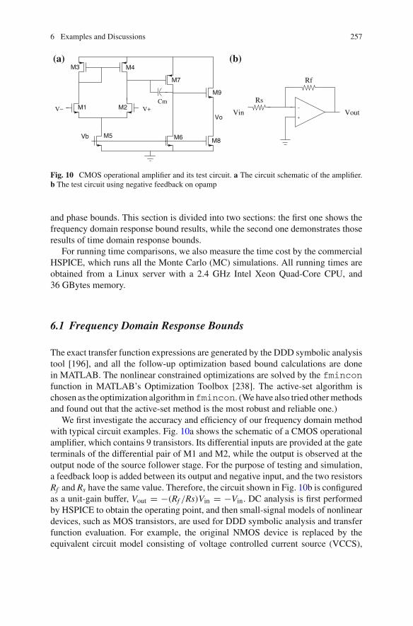
6 Examples and Discussions 257
M1 M2
M3 M4
M5 M6
M7
M8
M9
VoVi+
Vb
V+V−Cm
Rf
Rs
VoutVin+
−
(a) (b)
Fig. 10 CMOS operational amplifier and its test circuit. a The circuit schematic of the amplifier.b The test circuit using negative feedback on opamp
and phase bounds. This section is divided into two sections: the first one shows thefrequency domain response bound results, while the second one demonstrates thoseresults of time domain response bounds.
For running time comparisons, we also measure the time cost by the commercialHSPICE, which runs all the Monte Carlo (MC) simulations. All running times areobtained from a Linux server with a 2.4 GHz Intel Xeon Quad-Core CPU, and36 GBytes memory.
6.1 Frequency Domain Response Bounds
The exact transfer function expressions are generated by the DDD symbolic analysistool [196], and all the follow-up optimization based bound calculations are donein MATLAB. The nonlinear constrained optimizations are solved by the fminconfunction in MATLAB’s Optimization Toolbox [238]. The active-set algorithm ischosen as the optimization algorithm infmincon. (We have also tried other methodsand found out that the active-set method is the most robust and reliable one.)
We first investigate the accuracy and efficiency of our frequency domain methodwith typical circuit examples. Fig. 10a shows the schematic of a CMOS operationalamplifier, which contains 9 transistors. Its differential inputs are provided at the gateterminals of the differential pair of M1 and M2, while the output is observed at theoutput node of the source follower stage. For the purpose of testing and simulation,a feedback loop is added between its output and negative input, and the two resistorsRf and Rs have the same value. Therefore, the circuit shown in Fig. 10b is configuredas a unit-gain buffer, Vout = −(Rf /Rs)Vin = −Vin. DC analysis is first performedby HSPICE to obtain the operating point, and then small-signal models of nonlineardevices, such as MOS transistors, are used for DDD symbolic analysis and transferfunction evaluation. For example, the original NMOS device is replaced by theequivalent circuit model consisting of voltage controlled current source (VCCS),

258 11 Performance Bound Analysis of Analog Circuits Considering Process Variations
Table 2 Variational parameters used in the CMOS opamp
Affected transistor Model parameter Nominal value Variation (%)
M1, M2 gm 1.48 × 10⁻⁵ −1 5gds 2.33 × 10⁻⁸ −1
Cgs 5.16 fFCgd 0.31 fF
M9 gm 1.23 × 10⁻⁴ −1 10gds 3.94 × 10⁻⁷ −1
gate-source capacitance (Cgs), gate-drain capacitance (Cgd), terminal resistance, andso on. We actually use the MOS small-signal model shown in Fig. 1, with singularnetwork elements like nullator and norators. The combination of these elements inthe MOS model behaves as an ideal VCCS. However, the properties of the nullator(who does not allow current flowing through it and provides zero voltage differencebetween its two terminals, i.e., the voltage values on nodes G and N are the same)and the norator (who allows any voltage across its two terminals and any currentflowing through it) allow us to formulate more compact equations than MNA [180].
For the CMOS opamp, we enumerate the variational parameters used in the exper-iments in Table 2. The variational parameters are introduced to transconductance(gm), resistors, and capacitors inside the transistor model. Since transistors in thedifferential pair are subjected to symmetry requirements, we apply a relatively smallvariation (5 %) on them. As a result, there are totally 10 variational parameters in thisexample. The active filter example has 7 variational parameters, which are modeledin a similar way. Note that we assume that information of the variational parame-ters listed in Table 2 have been characterized during device level variation modelingprocess based on the data from foundry. The parameters will take Gaussian distribu-tions with their 3-sigma bounds ([μ−3σ,μ+3σ ], where μ is the mean and σ is thestandard deviation of the Gaussian variable) matching the bounds listed in Table 2.
After the symbolic expressions, i.e., numerator and denominator, of the opamp’stransfer function are obtained, the nominal frequency response can be evaluatedstraightforwardly using the specified parameter values. The lower and upper boundsof the magnitude and phase are then obtained by the aforementioned constrained opti-mization. Fig. 11 plots the nominal magnitude curve along with its lower and upperbounds. On the same figure, we also plot the 3-sigma bounds calculated from 5,000MC samples of the same circuits. It is obvious that our bounds include all possiblevariations, and do not show much over-conservativeness. The result demonstratesthe effectiveness of the optimization-based method to find accurate bounds.
We also remark that for a fair comparison, both the MC method and the presentedperformance bound analysis method are applied to the same circuits with the samedevice models and statistical distributions of parameters.

6 Examples and Discussions 259
104
106
108
−2
−1
0
Freq (Hz)
Mag
nitu
de (
dB)
Fig. 11 Magnitude bounds of CMOS opamp using the presented method and MC simulations. Thethick solid curve is nominal magnitude response, the two thin solid curves are bounds from thepresented method, and dashed curves are 3-sigma bounds of 5,000 times MC analysis. It is obviousthat our bounds are tight and accurate if compared with MC bounds
Fig. 12 The histogram ofmagnitude distribution of theCMOS opamp at frequencyf = 1 MHz using 5,000times MC simulation. The twovertical lines are the boundsfrom the presented method,and the dashed curve is theestimated Gaussian pdf usingour bound information
−0.5 −0.4 −0.3 −0.2 −0.10
200
400
600
Magnitude (dB)
Num
ber
of o
ccur
renc
es
As an application of the presented method, we apply the presented method foranalog yield estimation. We illustrate this using the same opamp. The yield estimationis calculated using preset specification. For the CMOS opamp in Fig. 10, we set arequirement that the accepted circuit should have its gain larger than −0.35 dB atfrequency f = 1 MHz. HSPICE MC analysis with 5,000 samples gives the yieldas 93.9 %, and the histogram of all samples is drawn in Fig. 12. Meanwhile, thepredicted yield using the presented method is 94.5 %, which is fairly close to that ofthe MC analysis. The detailed statistics of the comparison are shown in Table 3. Withthe accurate calculation of performance bounds and the yield, the presented methodonly takes 3.8 s. This is a 22× speedup over the 5,000 MC simulations.
The presented algorithm is also applied to a CMOS active filter [147] (circuitdiagram not shown in this chapter). Fig. 13 shows the magnitude bounds togetherwith HSPICE MC results. In this figure, we show the curves of the presented method,the 3-sigma curves and 6-sigma curves from MC results. As we can see, the pre-sented method matches the 3-sigma curves very well. We remark that our parametervariations are mainly bounded by their 3-sigma ranges, which lead to a better matchwith 3-sigma responses of the MC analysis. The statistical data is listed in Table 4.A speedup of 13× is observed on this example.

260 11 Performance Bound Analysis of Analog Circuits Considering Process Variations
Table 3 Statistical information of the CMOS opamp circuit (comparison with 5,000 times MC)
CMOS opamp
Runtime (s) MC 85.2Presented 3.8
Mean value (μ) MC −0.29Unit: dB Presented −0.29Std. value (σ ) MC 0.0365Unit: dB Presented 0.0367Yield rate MC 93.9 %
Presented 94.5 %
100
105
−40
−20
0
20
freq (Hz)
Mag
nitu
de (
dB)
104.5
104.6
104.7
24
25
26
27
28
29
30
freq (Hz)
Mag
nitu
de (
dB)
NominalMonte Carlo 3 sigma
Proposed method
Proposed method
Monte Carlo 3 sigma
Monte Carlo 6 sigma
Monte Carlo 6 sigma
(a)
(b)
Fig. 13 Comparison of bounds from MC and the presented method of magnitude response ofactive filter. The MC bounds are calculated as 3-sigma and 6-sigma bounds of 5,000 samples. Itis noticeable that our bounds capture MC’s 3-sigma bounds accurately. a Magnitude response ofthe active filter on the frequency sweep range. This circuit is more sensitive to variation between104 and 105 Hz. b Detailed comparison of magnitude bounds from the presented method and MCaround 104.5 Hz. The bounds from our method and the 3-sigma and 6-sigma bounds of MC samplesare properly annotated in the figure

6 Examples and Discussions 261
Table 4 Statisticalinformation of the CMOSfilter (comparison with 5,000times MC)
CMOS Filter
Runtime (s) MC 100.4Presented 8.2
Mean value (μ) MC 26.83Unit: dB Presented 26.81Std. value (σ ) MC 0.389Unit: dB Presented 0.384Yield rate MC 82.7 %
Presented 84.2 %
6.2 Time Domain Response Bounds
Using the frequency domain bounds we calculated in the previous experiments, thetime domain bounds of the CMOS opamp are obtained by the TIDBA method.Figure 14 shows bounds of 10,000 MC pulse responses at the output node of theopamp as dashed curves, and the bounds generated from TIDBA are overlaid ontothe same figure as solid curves.
We also simulated the active filter with a pulse waveform as input. Bounds of MCwaveforms observed at the output node are plotted as dashed curves in Fig. 15. Dueto the process variation of the filter, it can be observed that the output waveforms aredeviated from its nominal benchmark. Detailed plots of the up ramp and down rampare shown in Fig. 15b and c. The time domain performance bounds, computed byTIDBA, are plotted as solid curves. An input signal comprised of several sinusoidalwaves are also used to test this filter. Its possible minimum and maximum values intime domain and the TIDBA bounds are plotted in Fig. 16.
We notice that the bounds given by TIDBA may not be able to converge to thesteady state of the response, for example, after 0.06 s in Fig. 15a, which should bezero. This is due to the loss of dependence between magnitude and phase when weapply the frequency response bounds (2) and (3). However, for many steady states,which are known to be zero, even with variations in parameters, we can ignore thebounds given by the presented method. Another way to mitigate this problem isto directly compute time-domain bounds using the optimization based approaches,which will be investigated in our future works.
We remark that TIDBA seemingly over-estimates the performance bounds asshown in Figs. 14, 15, 16. But the results at least are conservative. The over-estimationis due to the nature of the presented algorithm as we formulate the problem into twophases. In the first phase, performance bounds are computed in frequency domain formagnitudes and phases independently. The second phase computes the time domainbounds based on the frequency domain bounds. Such a two-phase approach relaxessome properties of the signals going through analog systems in time domain. Forinstance, we lose the dependence between magnitudes and phases as we optimizethem separately. As a result, the two-phase method leads to relaxed optimizationproblem and thus over-estimated results.

262 11 Performance Bound Analysis of Analog Circuits Considering Process Variations
0 2 4 6 8
x 10−7
−0.1
0
0.1
0.2
0.3
0.4
0.5
0.6
time (s)
volta
ge (
V)
1.5 2 2.5
x 10−7
0.52
0.54
0.56
0.58
0.6
0.62
time (s)
volta
ge (
V)
(a)
(b)
Fig. 14 Time domain response of CMOS opamp with pulse input. Thick solid curve represent thenominal response. Thin solid curves are bounds from the TIDBA method, while dash curves arebounds of 10,000 MC results. a The whole plot, b detailed view around t = 2 × 10⁻⁷ s
Table 5 summarizes the experiment parameters and running time comparisons.The two examples still use the same variational parameter setup as in the frequencydomain experiments, and the MC transient simulation generates 10,000 samples.TIDBA takes a total number of 6,400 time domain samplings on input stimulus andfeeds them to FFT. The running time measurements of MC and TIDBA are also listedin the table. The maximum speedup of TIDBA over MC can be 38×.
6.3 Example and Discussions
Now we present some numerical results for second approach, which can computethe performance bounds in the time domain directly.

6 Examples and Discussions 263
0.04 0.045 0.05
0.2
0.4
0.6
0.8
time (s)
volta
ge (
V)
0.012 0.016 0.02 0.0240.2
0.3
0.4
0.5
0.6
0.7
0.8
time (s)
volta
ge (
V)
0.04 0.045 0.05
0.2
0.4
0.6
0.8
time (s)
volta
ge (
V)
(a)
(b) (c)
Fig. 15 Time domain response of the active filter with pulse wave input. The two solid curves arethe lower and upper bounds from the TIDBA method, and the dashed curves are bounds of 10,000MC simulations. The dot-dashed curve in the middle is the nominal transient response. a The wholeplot, b detail of up ramp, c detail of down ramp
Again, the DDD symbolic tool generates the exact transfer function expressionsfirst [196], and all the follow-up optimization based bound calculation and yieldestimation are done in MATLAB. The nonlinear constrained optimizations are solvedby the fmincon function in MATLAB’s Optimization Toolbox [238]. All running timeare sampled from a Linux server with a 2.4 GHz Intel Xeon Quad-Core CPU, and36 GB memory.
We compare presented method with standard Monte Carlo analysis in terms ofrunning time and accuracy using two examples. In all the examples, we assume that

264 11 Performance Bound Analysis of Analog Circuits Considering Process Variations
Fig. 16 Time domainresponse of the activefilter with sinusoidal waveinput. The two solid curvesare the lower and upper boundsfrom the presented method,while the dashed curves arebounds of 10,000 MC simu-lations. The dot-dashed curvein the middle is the nomi-nal response. a The wholeplot, b detailed view aroundt = 6 × 10⁻³ s
0.005 0.01 0.015 0.02−0.1
−0.05
0
0.05
0.1
time (s)
volta
ge (
V)
5 6 7
x 10−3
−0.05
0
0.05
0.1
time (s)
volta
ge (
V)
(a)
(b)
Table 5 Performancecomparison of TIDBA againstMC method (10,000 times)
Circuit name CPU time Speed upMC (10, 000) TIDBA
Opamp 362.9 s 11.2 s 32×Filter 459.7 s 12.1 s 38×
variational parameter has Gaussian distributions with the standard deviation σ . Theirvariational bound (3-sigma bound) will be [−3σ + μ, 3σ + μ] where μ is the meanof the random process.
6.4 An Interconnect RC Tree Circuit Example
The first example is an interconnect RC tree example, which is driven by a voltagesource as shown in Fig. 17.
The variational parameters are Ri = 0.1, i = 1, 2, 3, Cj = 0.1pf , j = 1, 2, 3.All parameters have 10 % variations, which means that, for presented method, theconstrained condition is (1 − 5 %) ∈ pstd ≤ p ≤ (1 + 5 %) ∈ pstd , for Monte Carloanalysis, σ = 1/6 ∈ 10 % ∈ pstd (3-sigma bound), in which, p represents the value ofa certain variational parameter, and pstd is the standard value of the parameter.

1 Introduction 265
Fig. 17 A RC tree circuit
Fig. 18 shows the transient step response 3-sigma bound of voltage of node 8with that from the presented method and simulation result from 5,000 MC runs. Thisfigure shows that the bounds from the presented method could safely cover the curvesfrom the Monte Carlo simulation. Fig. 19 shows 3-sigma bounds from 2,000 MCruns, 5,000 MC runs and the presented method at 0.5 ns.
We have several observations: First, the bounds given by the presented methodmatches with that given by the MC method very well. Since all of parameters take3-sigma bounds, the bounds computed by the presented method should be close to3-sigma bounds as well. If the output bounds are Gaussian, then 3-sigma will cover99.730 % area under the probability density function (pdf) of Gaussian distribution,which means we need to take at least 370 MC runs to have event to reach the bound.
Table 6 compares the runtime, voltage values of the presented method and that ofthe Monte Carlo method and also shows the error ratio of 2,000 MC runs, 5,000 MCruns. The table also shows that, our presented method has 8.3× speedup over 5,000MC run simulation.
To further study the bounds computed by the presented method, we compared3-sigma bounds given by 15K, 30K, 50K MC runs. Fig. 20a shows the 3-sigmaupper bound of V8 from the 15K, 30K, 50K runs of MC simulation and that fromthe presented method around 0.5 ns. In this figure, we observe that 3-sigma boundsgiven by 30K and 50K now go outside the bound of the presented method.
Figure 20b shows the 3-sigma lower bound of V8 from 15K, 30K, 50K runs ofMC simulation and the bound give by the presented method. In this case, we observe

266 11 Performance Bound Analysis of Analog Circuits Considering Process Variations
0 0.1 0.2 0.3 0.4 0.5 0.6 0.7 0.8 0.90
0.1
0.2
0.3
0.4
0.5
0.6
0.7
0.8
0.9
1
Time (ns)
V8
(v)
Lower bound from proposed methodUpper bound from proposed methodUpper bound from 5000 runs MCLower bound from 5000 runs MC
0.5 0.55 0.60.9
0.92
0.94
0.96
0.98
Fig. 18 The bounds of V8 obtained from 5,000 MC runs and the presented method on the RC treecircuit
0.5 0.51 0.52 0.53 0.54 0.55 0.56 0.57 0.58 0.59 0.60.9
0.91
0.92
0.93
0.94
0.95
0.96
0.97
Time (ns)
V8
(v)
Upper bound from proposed methodLower bound from proposed methodUpper bound from 5000 MC runsLower bound from 5000 MC runsUpper bound from 2000 MC runsLower bound from 2000 MC runs
Fig. 19 Comparison of bounds of V8 from 2,000 MC runs, 5,000 MC runs and the presentedmethod on the RC tree circuit
that the bound by the presented method contain ALL the bounds by different MCruns. This is a very interesting observation.
One possible explanation for the Fig. 20a, b is that the performance function maynot be monotonic function for the some of parameter variables (called non-monotonicparameters here). In other words, the min/max values of performance function maynot be reached at the edges of the bounds of those parameters. So the 3-sigma boundalready includes the values to reach the min/max values of the functions. This can

1 Introduction 267
Table 6 Comparison between the methods on lower bounds of V8 at t = 0.5 ns for the RC treecircuit
Method Samplings# CPU (s) Voltage (V) Error (%)
Monte Carlo 2,000 573.383 0.915 0.55Monte Carlo 5,000 1,490.798 0.912 0.22Presented method 1 180.432 0.910 N/A
0.5 0.5001 0.5002 0.5003 0.5004 0.5005 0.5006 0.5007 0.5008
0.934
0.9341
0.9342
0.9343
0.9344
0.9345
0.9346
0.9347
0.9348
0.9349
Time (ns)
V8
(v)
Upper bound from proposed method
Upper bound from 50K MC
Upper bound from 15K MC
Upper bound from 30K MC
Lower bound from 15K MC
Lower bound from 50K MC
Lower bound from proposed method
Lower bound from 30K MC
0.5 0.5001 0.5002 0.5003 0.5004 0.5005 0.5006 0.5007 0.5008
0.9081
0.9082
0.9083
0.9084
0.9085
0.9086
0.9087
0.9088
0.9089
0.909
Time (ns)
V8
(v)
Upper bound from proposed method
Upper bound from 50K MC
Upper bound from 15K MC
Upper bound from 30K MC
Lower bound from 15K MC
Lower bound from 50K MC
Lower bound from proposed method
Lower bound from 30K MC
(a) (b)
Fig. 20 Comparison of 3-sigma upper and lower bounds of V8 from 15K MC runs, 30K MC runs,50K MC runs and the presented method on the RC tree circuit at 0.5 ns, a upper bounds b lowbounds
explain Fig. 20a, in which the maximum value is reached when most of variationalparameter values found are not at edges of the bound. As a result, new approachwill find more conservative bounds as those non-monotonic parameters reach theirmin/max values already. For Fig. 20b, on the other hand, the minimum value isreached when many variational parameters are at edges of the bound. However, it isalmost impossible for all variational parameters are at edge of bounds at the sametime considering the Gaussian distribution especially when the number of variationalparameter is large. Therefore, the bound computed by new approach close to the truebound and more MC run can only get closer to the bound, but can’t go beyond thetrue bound. As a result, we can see the new method tend to find the true bound moreefficient than the MC method, especially for performance functions which achievesmin/max values when many parameters are at edge of bounds, as it requires quite agreat amount of samplings to possibly get the maximum or minimum.
To further study the behavior of the presented method, we perform 4-sigma boundanalysis in which the bounds of each parameters will be [−4σ +μ, 4σ +μ]. Fig. 21ashows the 4 sigma upper bounds from 100K MC runs, 200K MC runs and thepresented method at 0.1 ns. Figure 21b shows the 4-sigma lower bounds from 100KMC runs, 200K MC runs and that from the presented method at 0.1 ns. From thetwo figures we can see, that in this case, the presented method contain both upperbounds and lower bounds from the MC runs (even with 200K MC). It means that

268 11 Performance Bound Analysis of Analog Circuits Considering Process Variations
0.1 0.1005 0.101 0.1015 0.102 0.1025
0.352
0.354
0.356
0.358
0.36
0.362
0.364
0.366
Time (ns)
V8
(v)
Lower bound from 200K runs MCLower bound from 100K MC runsUpper bound from 100K runs MCLower bound from proposed methodUpper bound from proposed methodUpper bound from 200K runs MC
0.1 0.1002 0.1004 0.1006 0.1008 0.101 0.1012 0.1014 0.1016 0.1018
0.322
0.323
0.324
0.325
0.326
0.327
0.328
0.329
Time (ns)
V8
(v)
Lower bound from 200K runs MCLower bound from 100K MC runsUpper bound from 100K runs MCLower bound from proposed methodUpper bound from proposed methodUpper bound from 200K runs MC
(a) (b)
Fig. 21 Comparison of 4-sigma upper and lower bounds of V8 from 100K MC runs, 200K MCruns and the presented method on the RC tree circuit at 0.1 ns, a upper bounds, b low bounds
4-sigma upper bound computed by our method is large than 4-sigma bounds of MCsimulation. On the other hand, for the lower bounds, we observe the same results as3-sigma bound results: the presented method is always lowest bound among all themethods.
As a result, it can be seen that the presented method is more efficient to find thehigh sigma bounds, as it takes almost the same computational costs as computinglow sigma bounds, than the standard MC methods, whose computational costs go upalmost exponentially with high sigma bounds.
6.5 An Opamp Circuit Example
The second example is an opamp circuit with 7 MOSFETs as shown in Fig. 22a. Toperform the bound analysis, we use a linearized and simplified device models forthe MOSFETs as shown in Fig. 1. The variable parameters are M1.gm = 1.5 ∈ 10−5,M1.Cgd = 0.5fF, M1.Cgs = 5fF, M2.gm = 1.5 ∈ 10−5−1, M2.Cgd = 0.5fF,M2.Cgs = 5Ff , M5.rds = 5 ∈ 107, M6.rds = 5 ∈ 107 . Again all parameters have10 % variations.
Fig. 23 shows the transient response 3-sigma bound of Vout with sinusoidal waveinput obtained from presented method and simulation result from 5,000 MC runs.Fig. 24 shows the 3-sigma bounds from 2,000 MC runs, 5,000 MC runs, and thepresented method at 1ms. In this case, we observe that the bounds from the presentedmethod is still conservative such that it sill contain the bounds from all the MC runs.The possible reasons have been explained before.
Table 7 compares the runtime, voltage values of the presented method and that ofMonte Carlo method. It also shows the error ratio of 2,000 MC runs and 5,000 MCruns. It can been seen that the errors are quite small and get smaller as we take moreMC runs, which is the consistent with the MC method.

6 Examples and Discussions 269
(a)
(b)
Fig. 22 The opamp circuit and its MOSFET model, a an opamp circuit, b the simplified MOSFETmodel
0 200 400 600 800 1000 1200 1400 1600−2
−1.5
−1
−0.5
0
0.5
1
1.5
2
Time (us)
Vou
t (v)
600 605 610 615 620 6251.25
1.3
1.35
1.4
1.45
1.5
Upper bound from proposed methodLower bound from proposed methodUpper bound from 5000 MC methodLower bound from 5000 MC method
Fig. 23 The bounds from 5,000 MC runs and the presented method on the amplifier circuit
The same table also shows that, our presented method has 10.6× speedup over5,000 samplings MC simulation. We remark that, if high sigma (>3 sigma) bounds,the standard MC runs will increase rapid (almost exponentially), while the run timeof the presented method will remain the almost the same as it only deal with differentparameter bounds with the same number of parameters. As a result, the presentedmethod indeed overcome the high sigma issues with the standard MC based method,which is the major advantage of the presented method over MC based methods.

270 11 Performance Bound Analysis of Analog Circuits Considering Process Variations
1000 1005 1010 1015 1020 1025 1030 1035 1040 1045 1050−0.96
−0.94
−0.92
−0.9
−0.88
−0.86
−0.84
Time (us)
Vou
t (v)
Upper bound from 2000 runs MCUpper bound from 5000 runs MCUpper bound from proposed method
Fig. 24 Comparison of upper bounds of Vout from 2,000 MC runs, 5,000 MC runs and the presentedmethod on the amplifier circuit
Table 7 Comparison between the methods on lower bounds of Vout at t = 1 ms for the amplifiercircuit
Method Samplings# CPU (s) Voltage (V) Error (%)
Monte Carlo 2,000 412.071 −0.942 3.7Monte Carlo 5,000 1112.597 −0.906 0.79Presented method 1 105.460 −0.899 N/A
7 Summary
In this chapter, we have presented a performance bound analysis flow of analogcircuits considering process variations in both time and frequency domains. Thenew method applies a graph-based analysis technique to derive the symbolic trans-fer functions of linear(ized) analog circuits. Then the problem of finding frequencyresponse bounds is formulated into a nonlinear constrained optimization problem,where the cost functions are magnitude and phase of the transfer function subjectto the linear constraints, which are the upper and lower bounds of process varia-tional parameters. The frequency domain bounds calculated in this way are accurateand show no over-conservativeness suffered by the previous approaches. Based onthe frequency response bounds, we further presented an algorithm to compute timedomain response bounds of circuits with any arbitrary input signals. Experimen-tal results from several analog benchmark circuits show that the presented methodgives the correct bounds verified by Monte Carlo (MC) analysis while it delivers oneorder of magnitude speedup over MC in both frequency and time domain. We havealso shown analog circuit yield analysis as an application of the frequency domainvariational bound analysis.

Chapter 12Statistical Parallel Monte-CarloAnalysis on GPUs
1 Introduction
It is well known that analog and mixed-signal circuits are very sensitive to the processvariations as many matchings and regularities are required. This situation becomesworse as technology continues to scale to 90 nm and below owing to the increasingprocess-induced variability [141, 170]. For example, due to an inverse-square-root-law dependence with the transistor area, the mismatch of CMOS devices nearlydoubles for each process generation less than 90 nm [95, 128]. To consider the impactsof process variations on circuit performance. Monte-Carlo based statistical approachis the most reliable solutions to this problem. But the prohibitive computational costsof Monte Carlo method perverts it from solving large analog circuits.
Parallel computing based on GPUs leverages massive many-core parallelismand can deliver significant performance improvements over traditional single-coreand existing general multi-core computing techniques. For instance, the state-of-the-art NVIDIA Kepler K20X GPU with 2,688 cores has a peak performance ofover 4 TFLOPS versus about 80–100 GFLOPS of Intel i7 series Quad-core CPUs[1, 96]. The recent advent of the general purpose GPU (GPGPU) has ignited stronginterest from the broader scientific community in the GPU as a general platformfor solving computationally intensive problems [66]. The introduction of new par-allel programming interfaces for general purpose computation, such as ComputerUnified Device Architecture (CUDA), Stream SDK, and OpenCL [7, 94, 143], andrecent OpenACC [2] language has made GPUs an attractive choice for developinghigh-performance scientific computation tools and solving practical engineering andscientific problems. GPGPUs (especially NVIDIA Tesla GPUs) now have been usedin most of top 10 supercomputers in the world [3] as the main computing platformsinstead of just as accelerators. Parallelization on GPU platforms is an emergingstrategy to improve the efficiency of Monte-Carlo based statistical analysis method.But traditional numerical simulators based on LU decomposition such as SPICEis difficult to be parallelized on GPUs due to irregular memory access and hugememory-intensive operations.
G. Shi et al., Advanced Symbolic Analysis for VLSI Systems, 271DOI: 10.1007/978-1-4939-1103-5_12,© Springer Science+Business Media New York 2014

272 12 Statistical Parallel Monte-Carlo Analysis on GPUs
Graph-based symbolic technique is a viable tool for modeling the behavior orcharacteristic of analog circuits [61]. The introduction of determinant decision dia-grams based symbolic analysis technique (DDD) allows exact symbolic analysisof much larger analog circuits than all the other existing approaches [196, 197].Furthermore, with hierarchical symbolic representations [232, 236], exact symbolicanalysis via DDD graphs essentially allows the analysis of arbitrary large analogcircuits. Once the small-signal characteristics of circuits are presented by DDDs,evaluation of DDDs, whose CPU time is proportional to the size of DDDs, will giveexact numerical values. One important observation is that the DDD-based simulationis very amenable for parallel computing as the main computation is distributed toeach DDD node (via graph traversals) and the data dependency is very simple dueto the simple binary graph structure.
In this chapter, we present an efficient parallel graph-based simulation techniquebased on GPU computing platforms for Monte-Carlo based statistical analysis ofanalog circuits. We design novel data structures to represent the DDD graphs in theGPUs to enable fast memory access of massive parallel threads for computing thenumerical values of DDD graphs. The new method is inspired by inherent data paral-lelism and simple data independence in the DDD-based numerical evaluation process.Numerical results show that the new evaluation algorithm can achieve about one totwo orders of magnitudes speedup over the serial CPU based evaluations of analogcircuits and 2–3 times speedup over numerical SPICE-based simulation method onsome large analog circuits. Further more, the presented parallel techniques can beused for the parallelization of many more decision diagrams based applications, suchas logic synthesis, optimization and formal verifications, which are based on binarydecision diagrams (BDDs) and its variants [16, 135].
This chapter is organized as follows. Section 2 outlines DDD-based symbolicanalysis techniques. Then, we introduce the flow of the presented GPU Monte Carlosimulation. Section 4 describes the presented GPU parallel algorithm, followed byseveral numerical examples in Sect. 5. Last, Sect. 6 concludes the chapter.
2 Review of GPU Architectures
CUDA (short for Compute Unified Device Architecture) is the parallel computingarchitecture for Nvidia many-core GPU processors. The architecture of a typicalCUDA-capable GPU is consisted of an array of highly threaded streaming multi-processors (SM) and comes with up to 4–6 GB DRAM for Fermi GPUs, referredto as global memory. Each SM has eight streaming processor (SP) and two specialfunction units (SFU) and possesses its own shared memory and instruction cache.The structure of a streaming multiprocessor is shown in Fig. 1.
As the programming model of GPU, CUDA extends C into CUDA C and supportssuch tasks as threads calling and memory allocation, which makes programmersable to explore most of the capabilities of GPU parallelism. In CUDA programmingmodel, threads are organized into blocks; blocks of threads are organized as grids.

2 Review of GPU Architectures 273
Fig. 1 Structure of streaming multiprocessor
CUDA also assumes that both the host (CPU) and the device (GPU) maintain theirown separate memory spaces in DRAM, referred to as host memory and devicememory, respectively. For every block of threads, a shared memory is accessible toall threads in that same block. And the global memory is accessible to all threads in allblocks. Developers can write programs running millions of threads with thousands ofblocks in a parallel approach. This massive parallelism forms the reason that programswith GPU acceleration can be multiple times faster than their CPU counterparts.
One thing to mention is that for current GPU, a multiprocessor has eight single-precision floating point ALUs (one per core) but only one double-precision ALU(shared by the eight cores). Thus, for applications whose execution time is dominatedby floating point computations, switching from single-precision to double-precisionwill decrease performance by a factor of approximately eight. However, this situationis being improved. More recent GPU from Nvidia can already provide much betterdouble-precision performance than before.
3 The Graph-Based Parallel Statistical Analysis
In this section, we first provides an overview of our graph-based GPU-based parallelstatistical analysis before the detailed explanation.
As mentioned before, in DDD-based analysis, computing numerical value of thedeterminant of the DDD essentially boils down to the depth-first traversal of the

274 12 Statistical Parallel Monte-Carlo Analysis on GPUs
DDD symbolic analysis
Compute transfer functions
Assign random parameters to GPU side
Memory copy from host to device
Required number of MC trials reached?
Get distribution
MNA element sand DDD nodes
Save transfer functionsMemory copy from device to host
Levelize DDD data structureand save in continuous vectors
Yes
No
SPICE netlist with variation specified
Levelwise DDD tree evaluations
Fig. 2 The flow of GPU-based parallel Monte Carlo analysis
graph. The data dependency is very simple: a node can be evaluated only afterits children are evaluated. Such dependency implies the parallelism where all thenodes satisfying this constraint can be evaluated at the same time. Also, in statisticalfrequency analysis of analog circuits, evaluation of a DDD node at different frequencypoints and different Monte-Carlo runs can be performed in parallel. We show that allthose parallelism will be explored by the new statistical analysis approach on GPUplatforms.
3.1 The Overall Algorithm Flow
Figure 2 gives the overall flow of our statistical method. The whole algorithm has twomain parts, the CPU part (host) and GPU part (device) as clearly marked in the figure.CPU part mainly reads the netlist, generate the original DDD tree structures and buildsnew continuous DDD vector array structure (for GPU) and outputs the final numericalresults. GPU part takes care of the main parallel DDD evaluation and communicateswith CPU. The new program reads input netlist containing variation informationof the relevant circuit devices. Then, the analyzer builds the MNA (modified nodalanalysis) matrix and DDD binary tree data structure [196] as shown in step ①.

3 The Graph-Based Parallel Statistical Analysis 275
9210 3 4 5 6 7 8 node index
0 1 1 2 2 3 4 530
left child index
right child index−2 −2 −2 8−2 −2−2
−1
−2
−1 1 0
2
0 3
5
4 4 7 6
level index
data of one DDD node
cj ah i e g f d b DDD node value
kernel execution, loop over all levels
Active threads
Fig. 3 Levelized continuous storage of a DDD, and levelwise GPU evaluation of the DDD in Fig. 3in Chap. 4
3.2 The Continuous and Levelized DDD Structure
To prepare for the GPU computing, we need to build new data structures from theoriginal binary tree DDD structures. This will be done in the CPU as the constructiononly needs to be performed once and traversal of original DDD linked trees is stillsequential in nature and will be difficult to handle in GPU, as labeled ② in Fig. 2.
For GPU computing, the main challenge is to allow fast memory access by threadsor reduce memory traffic as much as possible by using shared memory (or texturememory) within blocks so that GPU cores can be busy all the time. In GPU, fastglobal memory access by threads can be done by coalesced memory access wherea half warp (or a warp) of threads (16 or 32 threads respectively) can read theirdata from the global memory in one read access. Coalesced memory access requiresthat data are arranged continuously in memory and consecutive with respective toinvolved thread indexes. As a result, we need to remap the linked DDD trees into amemory-continuous data structure.
The second issue is that we do not need to perform the DDD node evaluation forall the DDD nodes. Only those nodes whose children have been evaluated should becomputed by threads (one thread for one DDD node). This can be done by sortingthe DDD nodes by their level. Two DDD nodes have same level if they have the samenumber of edges on their longest path to the 1-terminal. For instance, node g andnode f has the same level in Fig. 3 in Chap. 4. DDD nodes at the same level can becomputed in parallel in GPU. As we can see, the largest level of DDD nodes will bebounded by the numbers of non-zeros in a determinant. But practically, number oflevel can be much less than the number of non-zeroes. For instance, we have 5 levelsin the DDD shown in Fig. 3 in Chap. 4 versus 10 nonzero elements.
In the new DDD structure, all the DDD nodes at the same level will be put incontinuous and consecutive memories (mainly the vself and future vtree values) andbe assigned to threads (one DDD node per thread) at the same time (one kernel

276 12 Statistical Parallel Monte-Carlo Analysis on GPUs
launch). The level assignment can be done by simple depth-first traversal of theDDD graph. After this, we can allow the continuous memory for all the DDD nodesfor one level starting from the lowest level until the highest level. We use the DDDexample in Fig. 3 in Chap. 4 again to illustrate the new data structure shown in Fig. 3.
For each value associated with a DDD node such as its value (vself ), left childindex, right child index, level index, sign (not shown), a linear array will be generatedbased on the level indexes of DDD node. For example, node b in Fig. 3 in Chap. 4becomes the 7-th element in the vector, and the index of its children, g and 0-terminal,are 4 and −2 accordingly. Note that, by our definition, 1-terminal’s index is −1, and0-terminal’s is −2. Those arrays then will be copied into GPU memory for futureDDD evaluation.
Figure 3 also shows the execution pattern of GPU threads during DDD evaluationwhere we start with the DDD nodes in the lowest level and continue one level ata time until we hit the highest level. Since all nodes of the same level have beenreorganized into one continuous memory segment, the active GPU threads workingon them can achieve coalesced read/write access and also minimize the occurrence ofbranch divergence. As we observed, consecutive and levelwise data format improvesthe performance of GPU by 2–3× for large sized circuits.
4 The Parallel GPU-Based Monte-Carlo Analysis Method
4.1 Random Number Assignment to MNA Elements and DDDNodes
For statistical analysis, we need to generate variations from devices into the elementsof the determinant and then into the data in the continuous DDD data structure. Due toMNA formulation, each device may appear 4 positions in a MNA matrix. Hence wetrack and save the MNA stamp patterns of circuit devices, and also their locations inDDD, during DDD construction. These data are transferred to GPU texture memoryas texture memory are read-only and can be accessed much faster than GPU globalmemory.
Next, in random number assignment, CURAND libray is used to generate vari-ations on nominal values of circuit parameters in GPU kernel function. We need tomake sure that one device variation, which may appear in 4 position in the MNAwill take the same value and this also reflect on the f the four DDD nodes will reflectthe same change. This is done in Line 2 and Line 3 of the pseudo-code in Algorithm4. The variations introduced in our experiments are Gaussian random values, whosemeans and deviations can be specified by users from input netlist.
Note that since we perform the frequency domain analysis, we need to evaluatethe MNA and DDD on all frequency points of interest. To enable coalesced memoryaccess to compute DDD values for many frequencies, as Line 5 and Line 8, the DDDcontinuous structure will be further changed so that all frequency responses of the

4 The Parallel GPU-Based Monte-Carlo Analysis Method 277
Algorithm 4 Parallel random value assignment for DDD nodes1: for all Monte Carlo runs do // launch threads in grids2: Assign random numbers to involved device parameters and stamp MNA elements.3: Save each DDD node’s admittance, capacitance, and inductance components as R[k] =
{g, c, l}.4: for all DDD nodes do // launch threads in grids5: Load frequency values to f .6: for all frequencies do // launch threads in a block7: vself [i] = R[k].g + j · (R[k].c · f [i] + R[k].l/ f [i])8: Save vself .
same element or node reside in consecutive memory addresses. We observe that thisfrequency related calculation is very suitable for intra-block GPU computing as allthe threads in a block can share the same DDD information (except for the frequencyvalues).
In GPU, the threads are organized into grids (can be two dimensional) and numberof grids can be as large as 64K or more in Kepler GPUs and each grid contains ablock and each block can have as many as 1,024 threads (in current GPU familiesfrom NVIDIA) and they can be organized in 3 dimensions. Threads in a block cancommunicate via shared or texture memory and can be explicitly synchronized. Inour problem, the dimension of the grid is set to NMC × |DDD|, i.e., the numberof Monte Carlo runs times the number of DDD nodes (assume that it is less than64K) and each block of this grid contains TILE_DIM threads, where TILE_DIM ismultiply of 16 to enable coalesced access on neighboring frequency responses andis also set with consideration of available GPU resources per block. In practice, weset TILE_DIM = 256. So we can allow to compute 256 frequency responses for oneDDD node. Notice that all the three FOR loops in Algorithm 4 will be replaced bymassive thread launches in parallel. The two outer FOR loops are parallelized at gridlevel, and the innermost FOR loop is parallelized at block level. Hence, the DDDnode values vself are computed for all Monte Carlo runs and all frequency points intheir respective blocks and threads (Line 7). If number of frequency points is largerthan TILE_DIM, the innermost FOR loop will be kept inside the kernel function.But instead of loop over each frequency point, we loop over TILE_DIM frequencypoints every time.
The number of Monte Carlo runs in each kernel launch is determined by the GPUspecification and the allocated resources, such as global memory, to each MonteCarlo calculation. For a typical µA741 circuit whose DDD contains 6,205 nodes and2,400 evaluated frequency points, the Tesla C2070 can allow 20 Monte Carlo runsin parallel. In case more runs are required, the steps from ③ through ⑥ in Fig. 2 arerepeated as many times as needed.

278 12 Statistical Parallel Monte-Carlo Analysis on GPUs
f0 f1 f2
a
fi
Gain
c
b
d
j
low
er le
vel n
odes
are
eva
luat
ed fi
rst.
f
Transfer functionMC#0
MC#1Data grid of parallel MC evaluationMC#0
MC#1
MC#NMC − 1
Each block represents one nodein a MC run.
GPU threads in each block evaluateone node on all frequencies.
MC#NMC − 1
fNf−1
Fig. 4 GPU parallel evaluation of the DDD in Fig. 3 in Chap. 4
Algorithm 5 Parallel Monte Carlo evaluation of DDDs1: for level=0 to top_level do // CPU host iteration2: for all Monte Carlo runs do // launch threads in grids3: for all DDD nodes do // launch threads in grids4: if node.level == level then5: Load vself of the current node, and vtree of its children.6: for all frequencies do // launch threads in a block7: Evaluate vtree for the current node by Eq. (3.3) on all frequencies.8: Save current node’s vtree.
4.2 Parallel Evaluation of DDDs
The evaluation of DDD is a process that computes the final numerical value of thedeterminant it represents. This procedure is labeled with ④ in Fig. 2. As we previouslydiscussed in Sect. 3.2, the data structure of DDD has been remapped to GPU friendlycontinuous and consecutive arrays and are sorted by level to enhance efficiency ofevaluation.
Similar to the GPU calculation of DDD node values mentioned in the previoussubsection, we also launch independent blocks for different Monte Carlo runs anddifferent DDD nodes, and use each thread block to calculate values of each node’svtree for all frequency points, which is depicted in Fig. 4.
Algorithm 5 lists the main flow of this algorithm. To ensure that the nodes areevaluated from bottom to top, the first FOR loop iterates the level index from 0 to

4 The Parallel GPU-Based Monte-Carlo Analysis Method 279
the maximum level in the DDD, and launches kernel function on the DDD nodes ofthe specific level, one at a time. Note that we keep this FOR loop in CPU control,instead of moving it inside the GPU kernel, in order to accomplish inter-block syn-chronization. This is necessary because we deploy the evaluation of different nodesin different thread blocks, and, if there is no synchronization, it is possible that a nodeof higher level gets evaluated before its children. Moreover, CUDA only providessynchronization among threads in a block, the kernel has to be finished if all blocksin the kernel grid are required to be synchronized. Therefore, in our implementation,the index of current level is passed into the kernel function as an argument, and thekernel will evaluate those thread blocks with the same level indicated by the argumentindex.
The coalesced memory access to the node’s vself and its children’s vtree values arealso ensured in the load and save operations in Line 5 and Line 8, because during theevaluation of the current node on all frequencies, the k-th thread will work on thek-th frequency, and all threads in a warp execute the same code path. Consequently,such a kernel launching exhibits a highly data intensive pattern, and reduces globalmemory traffic at the same time.
5 Examples
To show the performance of the presented GPU parallel Monte Carlo simulation, wetest the program on several industrial benchmark circuit netlists. For running timecomparisons, we also measure the time cost by the CPU version of DDD evaluationand HSPICE.
All of our programs are implemented in C++, with NVIDIA CUDA for the GPUcomputation part. All running time are sampled from a Linux server with an 2.4 GHzIntel Xeon Quad-Core CPU, and 36 GBytes memory. The GPU card installed on thisserver is Tesla C2070, which contains 448 cores running at 1.15 GHz and up to5 GBytes global memory.
Now let us investigate one typical example in detail. Fig. 5 shows the schematicof a µA741 circuit. This bipolar opamp contains 26 transistors and 11 resistors. DCanalysis is first performed by SPICE to obtain the operation point, and then small-signal model, shown in Fig. 6, is used for DDD symbolic analysis and numericalevaluation. The AC analysis is performed with the variation of several circuit com-ponents for Monte Carlo simulation. Several Monte Carlo samples of the magnituderesponse are plotted in Fig. 7. The 3-db bandwidth of all the statistics is calculatedand shown in the histogram in Fig. 8. In this example, the nominal 3-db frequency is1.2 kHz. As we can observe from Fig. 8, the histogram of the bandwidth frequencyis similar to the Gaussian distribution.
Next, we study the speedup and scalability of the GPU and CPU DDD based MonteCarlo simulations. The measurements of time taken by both programs running on thesame RC tree circuit are shown in Table 1, where different number of Monte Carloruns are tested. It is obvious that the speedup of GPU method over the CPU one is

280 12 Statistical Parallel Monte-Carlo Analysis on GPUs
Fig. 5 The circuit schematic of µA741
Fig. 6 The small signal model for bipolar transistor
significant. Also, when the number of Monte Carlo runs increases, GPU running timedoes not multiply as fast as the CPU version does, provided that the GPU resourcescan accommodate parallel execution of these Monte Carlo evaluations in one kernellaunch. Hence, in this way, all the GPU streaming multiprocessors are kept busy andthe throughput is maximized, which results in a striking speedup over the CPU serialversion.

5 Examples 281
Fig. 7 The cluster of frequency responses of the tested µA741 circuit
Fig. 8 Histogram diagram of the 3-db points for all these results
Last, we list the results of all benchmark tests in Table 2. The information ofthe circuits and their DDD representation is also included in the same table. The2nd through 5th column record number of nodes in circuit, number of elements inthe MNA matrix, number of DDD nodes in the generated DDD graph, number ofdeterminant product terms, respectively. The last three columns summarize the run-time of GPU parallel algorithm, serial algorithm and the HSPICE. The number ofMonte Carlo runs for all tests is set to 128. It is clear from this table that the GPU-accelerated version outperforms its CPU counterpart, and also achieves 2–3 timesspeedup over the commercial HSPICE on a variety of test circuits.

282 12 Statistical Parallel Monte-Carlo Analysis on GPUs
Table 1 Performance comparison of CPU serial and GPU parallel DDD evaluation for RC treecircuit
# MC runs GPU time (s) CPU time (s) Speedup
1 1.98 23.0 112 2.08 46.2 224 2.21 90.5 418 2.50 183.8 7316 3.03 364.1 12032 4.76 725.3 15264 8.68 1,442 166128 17.42 2,910 167
Table 2 Performance comparison of GPU, CPU, and HSPICE Monte Carlo simulations
Circuit # cir. # cir. |DDD| DDD GPU CPU HSPICEname nodes devices terms time (s) time (s) time (s)
bigtst 32 112 642 2.68 × 10⁷ 19.7 3143 38.4ccstest 9 35 109 260 0.80 108 2.5rlctest 9 39 119 572 1.05 145 2.6vcstst 12 46 121 536 0.73 104 3.8ladder21 22 64 64 28,657 2.10 365 5.1ladder100 101 301 301 9.27 × 10²⁰ 30.6 3,965 42.5rctree1 40 119 211 1.15 × 10⁸ 5.55 928 11.3rctree2 53 158 302 4.89 × 10¹⁰ 17.42 2,910 46.1µA741 23 89 6,205 363,914 59.1 6,243 73.6
6 Summary
In this chapter, we have presented a parallel statistical analysis method for largeanalog circuits using determinant decision diagram (DDD) based graph technique. Tomake it amenable for massively threaded based parallel computing GPU platforms,we designed novel data structures to represent the DDD graphs in the GPUs to enablefast memory access of massive parallel threads for computing the numerical valuesof DDD graphs. The new method is inspired by inherent data parallelism and simpledata independence in the DDD-based numerical evaluation process. Experimentalresults show that the new evaluation algorithm can achieve about one to two order ofmagnitudes speedup over the serial CPU based evaluations and 2–3× speedup overnumerical SPICE-based simulation method on some large analog circuits.

References
1. NVIDIA Tesla’s Servers and Workstations, http://www.nvidia.com/object/tesla-servers.html2. Openacc directives for accelerators, http://openacc-standard.org3. Top 500 supercomputers, http://www.top500.org/4. K. Agarwal, M. Agarwal, D. Sylvester, D. Blaauw, Statistical interconnect metrics for
physical-design optimization. IEEE Trans. Comput. Aided Des. Integr. Circuits Syst. 25(7),1273–1288 (2006)
5. K. Agarwal, D. Sylvester, D. Blaauw, F. Liu, S. Nassif, S. Vrudhula, Variational delay metricsfor interconnect timing analysis, in Proceedings of IEEE/ACM Design Automation Confer-ence (DAC), 2004, pp. 381–384.
6. S.B. Akers, Binary decision diagrams. IEEE Trans. Comput. 27(6), 509–516 (1978)7. AMD Inc., AMD Steam SDK, http://developer.amd.com/gpu/ATIStreamSDK, 20118. A.C., Antoulas, Approximation of Large-Scale Dynamical Systems (The Society for Industrial
and Applied Mathematics (SIAM), 2005).9. I. Asenova, Symbolic sensitivity analysis using nullators, norators and modified coates signal-
flow graph, in ELMAR, 2008, pp. 245–248.10. I.A. Awad, A.M. Soliman, The inverting second generation current conveyors: the missing
building blocks, CMOS realizations and applications. Int. J. Electron. 83(4), 413–432 (1999)11. D. Biolek, R. Senani, V. Biolkova, Z. Kolka, Active elements for analog signal processing:
classification, review, and new proposals. Radioengineering 17(4), 15–32 (2008)12. D.L. Boley, G.H. Golub, The Lanczos-Arnoldi algorithm and controllability. Syst. Control
Lett. 4, 317–324 (1984)13. K.S. Brace, R.L. Rudell, R.E. Bryant, Efficient implementation of a BDD package, in Pro-
ceedings of 27th ACM/IEEE Design Automation Conference, Orlando, FL, 1990, pp. 40–45.14. R.E. Bryant, Symbolic manipulatoin of Boolean functions using a graphical representation,
in Proceedings of 22nd ACM/IEEE Design Automation Conference (DAC), Las Vegas, NV,1985, pp. 688–694.
15. R.E. Bryant, Graph-based algorithms for boolean function manipulation. IEEE Trans. Com-put. 35(8), 677–691 (1986)
16. R.E. Bryant, Binary decision diagrams and beyond: enabling technologies for formal veri-fication, in Proceedings of International Conference on Computer Aided Design (ICCAD),1995.
17. R.E. Bryant, J.H. Kukula, Formal methods for functional verification, in The Best of ICCAD,20 Years of Excellence in Computer-Aided Design, ed. by A. Kuehlmann (Kluwer AcademicPublishers, Norwell, 2003), pp. 3–15
18. R.H. Byrd, R.B. Schnabel, G.A. Shultz, A trust region algorithm for nonlinearly constrainedoptimization. SIAM J. Numer. Anal. 24(5), 1152–1170 (1987). Available http://www.jstor.org/stable/2157645
G. Shi et al., Advanced Symbolic Analysis for VLSI Systems, 283DOI: 10.1007/978-1-4939-1103-5,© Springer Science+Business Media New York 2014

284 References
19. R. Cabeza, A. Carlosena, On the use of symbolic analyzers in circuit synthesis. Analog Integr.Circ. Sig. Process. 25(1), 67–75 (2000)
20. H.J. Carlin, Singular network elements. IEEE Trans. Circuit Theory 11(3), 67–72 (1964)21. A. Carlosena, G. Moschytz, Nullators and norators in voltage to current mode transformations.
Int. J. Circuit Theory Appl. 21(4), 421–424 (1993)22. R. Castro-López, O. Guerra, F. Fernández, A. Rodriguez-Vázquez, Synthesis of a wireless
communication analog back-end based on a mismatch-aware symbolic approach. AnalogIntegr. Circ. Sig. Process. 40(3), 215–233 (2004)
23. R. Chakraborty, M. Ranjan, R. Vemuri, Symbolic time-domain behavioral and performancemodeling of linear analog circuits using an efficient symbolic newton-iteration algorithm forpole extraction, in International Conference on VLSI Design, 2005, pp. 689–694.
24. H. Chen, C. Yeh, G. Wilke, S. Reddy, H. Nguyen, W. Walker, R. Murgai, A sliding windowscheme for accurate clock mesh analysis, in Proceedings of International Conference onComputer-Aided Design (ICCAD), Nov 2005, pp. 939–946.
25. L.H. Chen, M. Marek-Sadowska, Closed-form crosstalk noise metrics for physical designapplications, in Proceedings of European Design and Test Conference (DATE), Mar 2002,pp. 812–819.
26. W. Chen, G. Shi, Implementation of a symbolic circuit simulator for topological networkanalysis, in Proceedings of Asia Pacific Conference on Circuits and Systems (APCCAS),Singapore, Dec 2006, pp. 1327–1331.
27. J. Cheng, G. Shi, Symbolic computation of SNR for variational analysis sigma-delta mod-ulators, in Proceedings of Asia South-Pacific Design Automation Conference (ASPDAC),Singapore, 2014, pp. 443–448.
28. L.O. Chua, P.M. Lin, Computer-Aided Analysis of Electronic Circuits (Prentice Hall, NewJersy, 1975)
29. C.L. Coates, General topological formulas for linear network functions. IRE Trans. CircuitTheory 5(1), 42–54 (1958)
30. C.L. Coates, Flow graph solutions of linear algebraic equations. IRE Trans. Circuit Theory6(2), 170–187 (1959)
31. T. Cormen, C.E. Leiserson, R.L. Rivest, Introduction to Algorithms (The MIT Press, Cam-bridge, 1990)
32. Cygwin, Available http://www.cygwin.com/33. W. Daems, G. Gielen, W. Sansen, Circuit simplification for the symbolic analysis of analog
integrated circuits. IEEE Trans. Comput. Aided Des. Integr. Circuits Syst. 21(4), 395–406(2002)
34. W. Daems, G. Gielen, W. Sansen, A fitting approach to generate symbolic expressions forlinear and nonlinear analog circuit performance characteristics, in DATE, 2002, pp. 268–273.
35. L. Daniel, O.C. Siong, L.S. Chay, K.H. Lee, J. White, A multiparameter moment-matchingmodel-reduction approach for generating geometrically parameterized interconnect perfor-mance models. IEEE Trans. Comput. Aided Des. Integr. Circuits Syst. 23(5), 678–693 (2004)
36. A.C. Davies, The significance of nullators, norators and nullors in active network theory. IRETrans. 34, 256–267 (1967)
37. U. Desai, D. Pal, A transformation approach to stochastic model reduction. IEEE Trans.Automat. Contr. 29, 1097–1100 (1984)
38. S. Djordjevic, P. Petkovic, Generation of factorized symbolic network function by circuittopology reduction, in MIEL, 2004, pp. 773–776.
39. A. Doboli, R. Vemuri, A regularity-based hierarchical symbolic analysis methods for large-scale analog networks, IEEE Trans. Circuits Syst. II Analog Digital Sig. Process. 48(11),1054–1068 (2001).
40. T.S. Doorn, E.J W. ter Maten, J.A. Croon, A. Di Bucchianico, O. Wittich, Important samplingmonte carlo simulations for accurate estimation of SRAM yield, in IEEE ESSCIRC 2008–34thEuropean Solid-State Circuits Conference, 2008, pp. 230–233.
41. M. Duarte-Villasenor, E. Tlelo-Cuautle, L.G. de la Fraga, Binary genetic encoding for thesynthesis of mixed-mode circuit topologies. Circuits Syst. Sig. Process. 31(3), 849–863 (2012)

References 285
42. L. Dumitriu, M. Iordache, N. Voicu, Symbolic hybrid analysis of nonlinear analog circuits,in ECCTD, 2007, pp. 970–973.
43. T. Eeckelaert, W. Daems, G. Gielen, W. Sansen, Generalized simulation-based posynomialmodel generation for analog integrated circuits. Analog Integr. Circ. Sig. Process. 40(3),193–203 (2004)
44. M. Fakhfakh, E. Tlelo-Cuautle, R. Castro-Lopez, Analog/RF and Mixed-Signal Circuit Sys-tematic Design (Springer, Heidelberg, 2013)
45. M. Fakhfakh, E. Tlelo-Cuautle, F.V. Fernández (eds.), Design of Analog Circuits throughSymbolic Analysis (Bentham Science Publishers (e-Books), Oak Park, 2012)
46. P. Feldmann, R.W. Freund, Efficient linear circuit analysis by Padé approximation via theLanczos process, IEEE Trans. Comput. Aided Des. Integr. Circuits Syst. 14(5), 639–649(1995)
47. F.V. Fernández, O. Guerra, D.J. Roddríguez-Garcia, A. Roddríguez-Vázquez, Symbolic analy-sis of large analog integrated circuits: the numerical reference generation problem. IEEE Trans.Circuits Syst. II Analog Digital Sig. Process. 45(10), 1351–1361 (1998).
48. F.V. Fernández, A. Rodríguez-Vázquez, J.L. Huertas, A tool for symbolic analysis of analogintegrated circuits including pole/zero extraction, in Proceedings of European Conference onCircuit Theory and Design, 1991, pp. 751–761.
49. F.V. Fernández, A. Rodríguez-Vázquez, J.L. Huertas, G. Gielen (eds.), Symbolic AnalysisTechniques-Applications to Analog Design Automation (IEEE Press, New York, 1998)
50. F.V. Fernández, P. Wambacq, G. Gielen, A. Rodríguez-Vázquez, W. Sansen, Symbolic analy-sis of large analog integrated circuits by approximation during expression generation, inProceedings of IEEE International Symposium on Circuits and Systems (ISCAS), 1994,pp. 25–28.
51. J. Fernández-Bootello, M. Delgado-Restituto, A. Rodriguez-Vázquez, Matrix methods forthe dynamic range optimization of continuous-time g(m)-c filters. IEEE Trans. Circuits Syst.I Fundam. Theory Appl. 55(9), 2525–2538 (2008).
52. H. Floberg, Symbolic Analysis in Analog Integrated Circuit Design (Kluwer Academic Pub-lishers, Norwell, 1997)
53. C.A. Floudas, Nonlinear and Mixed-Integer Optimization: Fundamentals and Applications(Topics in Chemical Engineering) (Oxford University Press, Oxford, 1995)
54. R.W. Freund, SPRIM: structure-preserving reduced-order interconnect macromodeling, inProceedings of International Conference on Computer Aided Design (ICCAD), 2004,pp. 80–87.
55. S.J. Friedman, K.J. Supowit, Finding the optimal variable ordering for binary decision dia-grams. IEEE Trans. Comput. 39(5), 710–713 (1990)
56. M. Frigo, S.G. Johnson, The halfcomplex-format DFT in FFTW, MIT. Technical report, http://www.fftw.org/doc/The-Halfcomplex_002dformat-DFT.html
57. H.N. Gabow, Two algorithms for generating weighted spanning trees in order. SIAM J. Com-put. 6(1), 139–150 (1977)
58. P. Ghanta, S. Vrudhula, Variational interconnect delay metrics for statistical timing analysis,in Proceedings of International Symposium on Quality Electronic Design (ISQED), 2006,pp. 19–24.
59. G. Gielen, R. Rutenbar, Computer-aided design of analog and mixed-signal integrated circuits.Proc. IEEE 88(12), 703–717 (2000)
60. G. Gielen, W. Sansen, Symbolic Analysis for Automated Design of Analog Integrated Circuits(Kluwer Academic Publishers, Norwell, 1991)
61. G. Gielen, P. Wambacq, W.M. Sansen, Symbolic analysis methods and applications for analogcircuits: a tutorial overview. Proc. IEEE 82(2), 287–303 (1994)
62. G.E. Gielen, H. Walscharts, W. Sansen, ISAAC: a symbolic simulator for analog integratedcircuits. IEEE J. Solid-State Circuit 24(6), 1587–1596 (1989)
63. P.E. Gill, W. Murray, Michael, M.A. Saunders, An sqp algorithm for large-scale constrainedoptimization, Snopt. SIAM J. Optim. 12, 979–1006 (1997)

286 References
64. R. Giomi, A. Luchetta, Enhanced two-graph theory for symbolic analysis of electrical net-works, in Proceedings of 3rd International Workshop on Design of Mixed-Mode IntegratedCircuits and Applications, 1999, pp. 44–47.
65. K. Glover, All optimal Hankel-norm approximations of linear multi-variable systems andtheir L∞ error bounds. Int. J. Control 36, 1115–1193 (1984)
66. D. Göddeke, General-purpose computation using graphics hardware, http://www.gpgpu.org/,2011
67. G.H. Golub, C.F.V. Loan, Matrix Computations, 2nd edn. (The Johns Hopkins UniversityPress, Baltimore, 1989)
68. F. Grasso, A. Luchetta, S. Manetti, M. Piccirilli, A method for the automatic selection of testfrequencies in analog fault diagnosis. IEEE Trans. Instrum. Meas. 56(6), 2322–2329 (2007)
69. F. Grasso, S. Manetti, M. Piccirilli, A symbolic approach to design centering of analog circuits.Microelectron. Reliab. 47(8), 1288–1295 (2007)
70. O. Guerra, E. Roca, F.V. Fernández, A. Rodríguez-Vázquez, Approximate symbolic analysisof hierarchically decomposed analog circuits. Analog Integr. Circ. Sig. Process. 31, 131–145(2002)
71. O. Guerra, J. Rodriguez-Garcia, F. Fernández, A. Rodriguez-Vázquez, A symbolic pole/zeroextraction methodology based on analysis of circuit time-constants. Analog Integr. Circ. Sig.Process. 31(2), 101–117 (2002)
72. G.D. Hachtel, F. Somenzi, Logic Synthesis and Verification Algorithms (Kluwer AcademicPublishers, Norwell, 2000)
73. D.G. Haigh, T.J. W. Clarke, P.M. Radmore, Symbolic framework for linear active circuitsbased on port equivalence using limit variables. IEEE Trans. Circuits Syst. I Regul. Pap.53(9), 2011–2024 (2006).
74. D.G. Haigh, P.M. Radmore, Admittance matrix models for the nullor using limit variables andtheir application to circuit design, IEEE Trans. Circuits Syst. I Regul. Pap. 53(10), 2214–2223(2006)
75. Z. Hao, G. Shi, Symbolic techniques for statistical timing analysis of RCL mesh networkswith resistor loops, in Proceedings of International Symposium on Integrated Circuits (ISIC),Singapore, Dec 2009, pp. 470–473.
76. Z. Hao, G. Shi, A fast symbolic computation approach to statistical analysis of mesh networkswith multiple sources, in Proceedings of Asia South-Pacific Design Automation Conference(ASPDAC), Taiwan, China, 2010, pp. 383–388.
77. Z. Hao, G. Shi, S. X.-D. Tan, E. Tlelo-Cuautle, Symbolic moment computation for statisticalanalysis of large interconnect networks. IEEE Trans. Very Large Scale Integr. Syst. 21(5),944–957 (2013).
78. Z. Hao, S.X.-D. Tan, R. Shen, G. Shi, Performance bound analysis of analog circuits con-sidering process variations, in Proceedings of IEEE/ACM Design Automation Conference(DAC), CA, USA, June 2011, pp. 310–315.
79. P. Harshavardhana, E. Jonckheere, L. Silverman, Stochastic balancing and approximation-stability and minimality. IEEE Trans. Automat. Contr. 29, 744–746 (1984)
80. M. Hassoun, P.M. Lin, A new network approach to symbolic simulation of large-scale net-works, in Proceedings of IEEE International Symposium on Circuits and Systems (ISCAS),1989, pp. 806–809.
81. M.M. Hassoun, P.M. Lin, A hierarchical network approach to symbolic analysis of large-scalenetworks. IEEE Trans. Circuits Syst. I Fundam. Theory Appl. 42(4) 201–211 (1995).
82. M.M. Hassoun, K. McCarville, Symbolic analysis of large-scale networks using a hierarchicalsignal flowgraph approach. J. Analog VLSI Sig. Proces. 3, 31–42 (1993)
83. L. Hernes, W. Sansen, Distortion in single-, two- and three-stage amplifiers. IEEE Trans.Circuits Syst. I Fundam. Theory Appl. 52(5), 846–856 (2005).
84. J.-J. Hsu, C. Sechen, DC small signal symbolic analysis of large analog integrated circuits.IEEE Trans. Circuits Syst. I Fundam. Theory Appl. 41(12), 817–828 (1994).
85. W.-C. Huang, H.-Y. Wang, P.-S. Cheng, Y.-C. Lin, Nullor equivalents of active devices forsymbolic circuit analysis. Circuits Syst. Sig. Proces. 31(3), 865–875 (2012)
References 287
86. M. Iordache, L. Dumitriu, Efficient decomposition techniques for symbolic analysis of large-scale analog circuits by state variable method. Analog Integr. Circ. Sig. Process. 40(3), 235–253 (2004)
87. M. Iordache, L. Dumitriu, Multi-time method based on state equations for rf circuit analysis,in Proceedings of IEEE International Sympodium on Circuits and Systems (ISCAS), 2007,pp. 517–520.
88. M. Iordache, L. Dumitriu, Time domain diakoptic analysis based on reduced-order stateequations. Int. J. Bifurcat. Chaos 17(10), 3625–3631 (2007)
89. Y.I. Ismail, C.S. Amin, Computation of signal-threshold crossing times directly from higherorder moments, IEEE Trans. Comput. Aided Des. Integr. Circ. Syst. 23(8), 1264–1276 (2004)
90. R.W. Jensen, L.P. McNamee, Handbook of circuit analysis languages and techniques (PrenticeHall, New Jersy, 1976)
91. B. Kagstrom, P. V. Dooren, A generalized state-space approach for the additive decompositionof a transfer matrix. J. Linear Algebra Appl. (1992).
92. K.J. Kerns, A.T. Yang, Stable and efficient reduction of large, multiport RC network by poleanalysis via congruence transformations. IEEE Trans. Comput. Aided Des. Integr. CircuitsSyst. 16(7), 734–744 (1998)
93. V.L. Kharitonov, Asymptotic stability of an equilibrium position of a family of systems oflinear differential equations. Differential. Uravnen. 14, 2086–2088 (1978)
94. Khronos Group, Open Computing Language (OpenCL), http://www.khronos.org/opencl,2011
95. J. Kim, K. Jones, M. Horowitz, Fast, non-monte-carlo estimation of transient performancevariation due to device mismatch, in Proceedings of IEEE/ACM Design Automation Confer-ence (DAC), 2007.
96. D.B. Kirk, W.-M. Hwu, Programming Massively Parallel Processors: A Hands-on Approach,2nd edn. (Morgan Kaufmann Publishers Inc., San Francisco, 2013)
97. L. Kolev, V. Mladenov, S. Vladov, Interval mathematics algorithms for tolerance analysis.IEEE Trans. Circuits Syst. 35(8), 967–975 (1988)
98. Z. Kolka, M. Volkova, Implementation of graph-based symbolic simplification, in Interna-tional Conference on Radioekektronika, 2007, pp. 43–46.
99. G. Kron, Tensor Analysis of Networks (Wiley, New York, 1939)100. P. Kumar, R. Senani, Bibliography on nullors and their applications in circuit analysis, syn-
thesis and design. Analog Integr. Circ. Sig. Process. 33(1), 65–76 (2002)101. B.P. Lathi, Modern Digital and Analog Communication Systems, 3rd edn. (Oxford University
Press, Oxford, 1998)102. A.J. Laub, M.T. Heath, C.C. Paige, R.C. Ward, Computation of system balancing trans-
formations and other applications of simultaneous diagonalization algorithms. IEEE Trans.Automat. Contr. 32, 115–122 (1987)
103. C.Y. Lee, Representation of switching circuits by binary-decision programs. Bell Syst. Tech.J. 38, 985–999 (1959)
104. H.J. Lee, C.C. Chu, W.-S. Feng, Moment computations of nonuniform distributed coupledRLC trees with applications to estimating crosstalk noise, in Proceedings of InternationalSymposium on Quality Electronic Design (ISQED), 2004, pp. 75–80.
105. H.-J. Lee, M.-H. Lai, C.-C. Chu, W.-S. Feng, Applications of tree/link partitioning for momentcomputations of general lumped RLC networks with resistor loops, in Proceedings of IEEEInternational Symposium on Circuits and Systems (ISCAS), 2004, pp. 713–716.
106. H.-J. Lee, M.-H. Lai, C.-C. Chu, W.-S. Feng, Moment computations for R(L)C interconnectswith multiple resistor loops using ROBDD techniques, in Proceedings of IEEE Asia-PacificConference on Circuits and Systems (APCCAS), 2004, pp. 525–528.
107. J.Y. Lee, X. Huang, R.A. Rohrer, Pole and zero sensitivity calculation in asymptotic waveformevaluation. IEEE Trans. Comput. Aided Des. 11(5), 586–597 (1992)
108. F. Leyn, G. Gielen, W. Sansen, Analog small-signal modeling–part I: behavioral signal pathmodeling for analog integrated circuits. IEEE Trans. Circuits Syst. II Analog Digital Sig.Proces. 48(7), 701–711, (2001).

288 References
109. F. Leyn, G. Gielen, W. Sansen, Analog small-signal modeling–part II: elementary transistorstages analyzed with behavioral signal path modeling. IEEE Trans. Circuits Syst. II AnalogDigital Sig. Process. 48(7), 701–711 (2001).
110. D. Li, S. X.-D. Tan, B. McGaughy, ETBR: extended truncated balanced realization method foron-chip power grid network analysis, in Proceedings of European Design and Test Conference(DATE), 2008, pp. 432–437.
111. J.R. Li, Model reduction of large linear systems via low rank system gramians. Ph.D. thesis,MIT, 2002.
112. J.R. Li, F. Wang, J. White, An efficient Lyapunov equation-based approach for generatingreduced-order models of interconnect, in Proceedings of IEEE/ACM Design AutomationConference (DAC), 1999, pp. 1–6.
113. P. Li, L.T. Pileggi, Compact reduced-order modeling of weakly nonlinear analog and rf cir-cuits, IEEE Trans. Comput. Aided Des. Integr. Circuits Syst. 23(2), 184–203 (2005)
114. X. Li, P. Li, L. Pileggi, Parameterized interconnect order reduction with explicit-and-implicitmulti-parameter moment matching for inter/intra-die variations, in Proceedings of Interna-tional Conference on Computer-Aided Design (ICCAD), Nov 2005, pp. 806–812.
115. X. Li, H. Xu, G. Shi, A. Tai, Hierarchical symbolic sensitivity computation with applicationsto large amplifier circuit design, in Proceedings of International Conference on Circuits andSystems (ISCAS), Rio de Janeiro, Brazil, 2011, pp. 2733–2736.
116. Y.-T. Li, Z. Bai, Y. Su, X. Zeng, Model order reduction of parameterized interconnect networksvia a two-directional Arnoldi process. IEEE Trans. Comput. Aided Des. Integr. Circuits Syst.27(9), 1571–1582 (2008)
117. P.M. Lin, Symbolic Network Analysis (Elsevier Science Publishers B.V, New York, 1991)118. P.M. Lin, Sensitivity analysis of large linear networks using symbolic programs, in Proceed-
ings of IEEE International Symposium on Circuits and Systems (ISCAS), San Diego, 1992,pp. 1145–1148.
119. W.-C. Lin, H.-Y. Wang, C.-Y. Liu, T.-F. Lee, Symbolic analysis of active device containingdifferencing voltage or current characteristics. Microelectron. J. 44(4), 354–358 (2013)
120. B. Liu, J. Messaoudi, G. Gielen, A fast analog circuit yield estimation method for mediumand high dimensional problems, in Proceedings of Design, Automation, and Test in Europe(DATE), 2012, pp. 751–756.
121. X. Liu, A. Palma-Rodriguez, S. Rodriguez-Chavez, S. X.-D. T.E. Tlelo-Cuautle, Y. Cai, Per-formance bound and yield analysis for analog circuits under process variations, in Proceedingsof Asia South Pacific Design Automation Conference (ASPDAC), Jan 2013, pp. 761–766.
122. X. Liu, S. X.-D. Tan, Z. Hao, G. Shi, Time-domain performance bound analysis of analog cir-cuits considering process variations, in Proceedings of Asia South Pacific Design AutomationConference (ASPDAC), Jan 2012.
123. Y. Liu, L. T. Pileggi, A.J. Strojwas, Model order-reduction of rc(l) interconnect includingvariational analysis, in DAC ’99: Proceedings of the 36th ACM/IEEE Conference on DesignAutomation, 1999, pp. 201–206.
124. J.D. Ma, R.A. Rutenbar, Fast interval-valued statistical modeling of interconnect and effectivecapacitance. IEEE Trans. Comput. Aided Des. Integr. Circuits Syst. 25(4), 710–724 (2006)
125. J.D. Ma, R.A. Rutenbar, Interval-valued reduced-order statistical interconnect modeling, IEEETrans. Comput. Aided Des. Integr. Circuits Syst. 26(9), 1602–1613 (2007)
126. J.D. Ma, R.A. Rutenbar, Fast interval-valued statistical interconnect modeling and reduction,in Proceedings of the International Symposium on Physical Design (ISPD), 2005, pp. 159–166.
127. A. Manthe, L. Zhao, C.-J. Shi, Symbolic analysis of analog circuits with hard nonlinearity, inIEEE DAC, 2003, pp. 542–545.
128. H. Masuda, S. Ohkawa, A. Kurokawa, M. Aoki, Challenge: variability characterization andmodeling for 65- to 90-nm processes, in Proceedings of IEEE Custom Integrated CircuitsConference (CICC), 2005.
129. W. Mayeda, Graph Theory (Wiley-Interscience, New York, 1972)

References 289
130. W. Mayeda, S. Seshu, Topological formulas for network functions. Technical report, Univer-sity of Illinois, Urbana, 1959 (Engineering Experimentation Station, Bulletin 446).
131. T. McConaghy, G.E. Gielen, Globally reliable variation-aware sizing of analog integratedcircuits via response surfaces and structural homotopy. IEEE Trans. Comput. Aided Des.Integr. Circuits Syst. 28(11), 1627–1640 (2009)
132. D.G. Meyer, S. Srinivasan, Balancing and model reduction for second-order form linearsystems. IEEE Trans. Automat. Contr. AC-41, 1632–1644 (1996).
133. N. Mi, J. Fan, S.X.-D. Tan, Statistical analysis of power grid networks considering lognor-mal leakage current variations with spatial correlation, in Proceedings of IEEE InternationalConference on Computer Design (ICCD), 2006, pp. 56–62.
134. S. Minato, Zero-suppressed BDD’s for set manipulation in combinatorial problems, in Pro-ceedings of 30th IEEE/ACM Design Automation Conference, Dallas, TX, 1993, pp. 272–277.
135. S. Minato, Binary decision diagrams and applications for VLSI CAD (Kluwer Academic,Norwell, 1996)
136. G.J. Minty, A simple algorithm for listing all the trees of a graph. IEEE Trans. Circuit Theory12(1), 120 (1965)
137. N. Miskov-Zivanov, D. Marculescu, Circuit reliability analysis using symbolic techniques,IEEE Trans. Comput. Aided Des. Integr. Circuits Syst. 25(12), 2638–2649 (2006)
138. B.C. Moore, Principal component analysis in linear systems: controllability, observability,and model reduction, IEEE Trans. Autom. Control AC-26(1), 17–32 (1981).
139. R.E. Moore, Interval Analysis (Prentice-Hall, London, 1966)140. L.W. Nagel, D.O. Pederson, SPICE: Simulation Program with Integrated Circuit Emphasis,
ser. Memorandum ERL-M382. (Electronics Research Laboratory, University of California,California, Berkeley, 1973).
141. S. Nassif, Model to hardware correlation for nm-scale technologies, in Proceedings of IEEEInternational Workshop on Behavioral Modeling and Simulation (BMAS), Sept 2007 (keynotespeech).
142. U. Naumann, The Art of Differentiating Computer Programs: An Introduction to AlgorithmicDifferentiation, ser. Software, Environments, and Tools (SIAM, Philadelphia, 2012).
143. NVIDIA Corporation, CUDA (Compute Unified Device Architecture), http://www.nvidia.com/object/cuda_home.html, 2011
144. A. Odabasioglu, M. Celik, L.T. Pileggi, PRIMA: passive reduced-order interconnect macro-modeling algorithm. IEEE Trans. Comput. Aided Des. Integr. Circuits Syst. 17(8), 645–654(1998)
145. A.V. Oppenheim, R.W. Schafer, Discrete-Time Signal Processing (Prentice Hall, London,1999)
146. A.B. Owen, Latin supercube sampling for very high-dimensional simulations. ACM Trans.Model. Comput. Simul. 8(1), 71–102 (1998)
147. A.A. Palma-Rodriguez, E. Tlelo-Cuautle, S. Rodriguez-Chavez, S.X.-D. Tan, DDD-basedsymbolic sensitivity analysis of active filters, in Proceedings of International Caribbean Con-ference on Devices, Circuits and Systems (ICCDCS), Mar 2012, pp. 170–173.
148. S.K. Patnaik, S. Banerjee, Symbolic noise modeling, analysis and optimization of a CMOSinput buffer. Analog Integr. Circ. Sig. Process. 70(3), 293–302 (2012)
149. M. Pelgrom, A. Duinmaijer, A. Welbers, Matching properties of MOS transistors. IEEE J.Solid State Circuits 24, 1433–1439 (1989)
150. J. Phillips, Variational interconnect analysis via PMTBR, in Proceedings of InternationalConference on Computer Aided Design (ICCAD), Nov 2004, pp. 872–879.
151. J.R. Phillips, L. Daniel, L.M. Silveira, Guaranteed passive balancing transformation for modelorder reduction, IEEE Trans. Comput. Aided Des. Integr. Circuits Syst. 22(8), 1027–1041(2003)
152. J.R. Phillips, L.M. Silveira, Poor man’s TBR: a simple model reduction scheme, IEEE Trans.Comput. Aided Des. Integr. Circuits Syst. 24(1), 43–55 (2005)
153. M. Pierzchala, B. Rodanski, Generation of sequential symbolic network functions for large-scale networks by circuit reduction to a two-port. IEEE Trans. Circuits Syst. I Fundam. TheoryAppl. 48(7), 906–909 (2001).

290 References
154. L.T. Pillage, R.A. Rohrer, Asymptotic waveform evaluation for timing analysis. IEEE Trans.Comput. Aided Des. Integr. Circuits Syst. 9(4), 352–366 (1990)
155. C. Pritchard, B. Wigdorowitz, Improved method of determining time-domain transient per-formance bounds from frequency response uncertainty regions. Int. J. Control 66(2), 311–327(1997)
156. S. Pullela, N. Menezes, L.T. Pillage, Moment-sensitivity-based wire sizing for skew reductionin on-chip clock nets. IEEE Trans. Comput. Aided Des. Integr. Circuits Syst. 16(2), 210–215(1997)
157. Z. Qi, H. Yu, P. Liu, S.X.-D. Tan, L. He, Wideband passive multi-port model order reductionand realization of RLCM circuits. IEEE Trans. Comput. Aided Des. Integr. Circuits Syst.25(8), 1496–1509 (2006)
158. L. Qian, D. Zhou, S. Wang, X. Zeng, Worst case analysis of linear analog circuit performancebased on Kharitonov’s rectangle, in Proceedings of IEEE International Conference on Solid-State and Integrated Circuit Technology (ICSICT), Nov 2010.
159. Z. Qin, S.X.-D. Tan, C. Cheng, Symbolic Analysis and Reduction of VLSI Circuits (KluwerAcademic Publishers, Boston, 2005)
160. J.M. Rabaey, A. Chandrakasan, B. Nikolic, Digital Integrated Circuits–A Design Perspective,2nd edn. (Pearson Education Inc., Englewood Cliffs, 2003)
161. A. Rajaram, J. Hu, R. Mahapatra, Reducing clock skew variability via crosslinks, IEEE Trans.Comput. Aided Des. Integr. Circuits Syst. 25(6), 1176–1182 (2006)
162. A. Rajaram, D.Z. Pan, MeshWorks: an efficient framework for planning, synthesis and opti-mization of clock mesh networks, in Proceedings of Asia South-Pacific Design AutomationConference (ASPDAC), Mar 2008, pp. 250–257.
163. M. Ranjan, A. Bhaduri, W. Verhaegen, Use of symbolic performance models in layout-inclusive rf low noise amplifier synthesis, in IEEE BMAS, 2004, pp. 130–134.
164. C.L. Ratzlaff, L.T. Pillage, RICE: rapid interconnect circuit evaluation using AWE. IEEETrans. Comput. Aided Des. Integr. Circuits Syst. 13(6), 763–776 (1994)
165. P.J. Restle, T.G.M. et al., A clock distribution network for microprocessors. IEEE J. Solid-State Circuits 36(5), 792–799 (2001)
166. B. Rodanski, Extension of the two-graph method for symbolic analysis of circuits with non-admittance elements, in Proceedings of International Workshop on Symbolic Methods andApplications to Circuit Design, 2002, pp. 17–20.
167. J. Rodriguez-Garcia, O. Guerra, E. Roca, F. Fernández, A. Rodriguez-Vázquez, Error controlin simplification before generation algorithms for symbolic analysis of large analogue circuits.Electron. Lett. 35(4), 260–261 (1999)
168. R.A. Rohrer, Circuit partitioning simplified. IEEE Trans. Circuits Syst. 35(1), 2–5 (1988)169. G. Rozakis, A. Samelis, Symbolic/numerical nonlinear circuit analysis using volterra series,
in 36th European Microwave Conference, 2006, pp. 1610–1613.170. R. Rutenbar, Next-generation design and EDA challenges, in Proceedings of Asia South
Pacific Design Automation Conference (ASPDAC), Jan 2007 (keynote speech).171. R.A. Rutenbar, G.E. Gielen, B.A. Antao, Computer-aided Design of Analog Integrated Cir-
cuits and Systems (Wiley, NY, 2002)172. R.A. Saad, A.M. Soliman, Use of mirror elements in the active device synthesis by admittance
matrix expansion, IEEE Trans. Circuits Syst. I Regul. Pap. 55(9), 2726–2734 (2008)173. R.A. Saad, A.M. Soliman, A new approach for using the pathological mirror elements in the
ideal representation of active devices. Int. Circuit Theory Appl. 38, 148–178 (2010)174. R.A. Saad, A.M. Soliman, On the systematic synthesis of CCII-based floating simulators. Int.
J. Circuit Theory Appl. 38, 935–967 (2010)175. R. Saad, A. Soliman, Generation, modeling, and analysis of CCII-based gyrators using the
generalized symbolic framework for linear active circuits. Int. J. Circuit Theory Appl. 36(3),289–309 (2008)
176. M.G. Safonov, R.Y. Chiang, A Schur method for balanced truncation model reduction. IEEETrans. Automat. Contr. 34, 729–733 (1989)

References 291
177. S. Saibua, L. Qian, D. Zhou, Worst case analysis for evaluating VLSI circuit performancebounds using an optimization method, in IEEE/IFIP 19th International Conference on VLSIand System-on-Chip, 2011, pp. 102–105.
178. C. Sánchez-López, Pathological equivalents of fully-differential active devices for symbolicnodal analysis. IEEE Trans. Circuits Syst. I Regul. Pap. 60(3), 603–615 (2013).
179. C. Sánchez-López, B. Cante-Michcol, F.E. Morales-López, M.A. Carrasco-Aguilar, Patholog-ical equivalents of CMs and VMs with multi-outputs. Analog Integr. Circuits Signal Proces.75(1), 75–83 (2013)
180. C. Sánchez-López, F.V. Fernández, E. Tlelo-Cuautle, S. X.-D. Tan, Pathological element-based active device models and their application to symbolic analysis. IEEE Trans. CircuitsSyst. I Regul. Pap. 58(6), 1382–1395 (2011).
181. C. Sánchez-López, E. Martinez-Romero, E. Tlelo-Cuautle, Symbolic analysis of OTRAs-based circuits. J. Appl. Res. Technol. 9(1), 69–80 (2011)
182. C. Sánchez-López, D. Moro-Frias, E. Tlelo-Cuautle, Improving the formulation process ofthe system of equations of analog circuits, in SM2ACD, 2008, pp. 102–106.
183. C. Sánchez-López, E. Tlelo-Cuautle, Symbolic noise analysis in analog integrated circuits,in IEEE ISCAS, vol. V, 2004, pp. 245–248.
184. C. Sánchez-López, E. Tlelo-Cuautle, Symbolic noise analysis in Gm-C filters, in IEEECERMA, vol. I, 2006, pp. 49–53.
185. C. Sánchez-López, E. Tlelo-Cuautle, Novel SBG, SDG and SAG techniques for symbolicanalysis of analog integrated circuits, in SM2ACD, 2008, pp. 17–22.
186. C. Sánchez-López, E. Tlelo-Cuautle, Behavioral model generation of current-mode analogcircuits, in IEEE ISCAS, 2009, pp. 2761–2764.
187. C. Sánchez-López, E. Tlelo-Cuautle, M. Fakhfakh, M. Loulou, Computing simplified noise-symbolic-expressions in CMOS ccs by applying spa and sag, in IEEE ICM, 2007, pp. 159–162.
188. C. Sánchez-López, A. Ruiz-Pastor, R. Ochoa-Montiel, M. Angel Carrasco-Aguilar, Symbolicnodal analysis of analog circuits with modern multiport functional blocks. Radioengineering22(2), 518–525 (2013).
189. S.J. Seda, M.G.R. Degrauwe, W. Fichtner, A symbolic analysis tool for analog circuit designautomation, in Proceedings of International Conference on Computer Aided Design (ICCAD),Nov 1988, pp. 488–491.
190. S.J. Seda, M.G.R. Degrauwe, W. Fichtner, Lazy-expansion symbolic expression approxi-mation in synap, in Proceedings of International Conference on Computer Aided Design(ICCAD), Nov 1992, pp. 310–317.
191. A.S. Sedra, K.C. Smith, A second generation current conveyor and its applications. IEEETrans. Circuit Theory 17(1), 132–134 (1970)
192. C.E. Shannon, A symbolic analysis of relay and switching circuits. Trans. AIEE 57, 713–723(1938)
193. B.N. Sheehan, Realizable reduction of RC networks. IEEE Trans. Power Apparatus Syst.26(8), 1393–1407 (2007)
194. B.N. Sheehan, ENOR: model order reduction of RLC circuits using nodal equations forefficient factorization, in Proceedings of IEEE/ACM Design Automation Conference (DAC),1999, pp. 17–21.
195. C.-J.R. Shi, X.-D. Tan, Symbolic analysis of large analog circuits with determinant deci-sion diagrams, in Proceedings of IEEE/ACM International Conferemce on Computer-AidedDesign (ICCAD), San Jose, CA, 1997, pp. 366–373.
196. C.-J.R. Shi, X.-D. Tan, Canonical symbolic analysis of large analog circuits with determinantdecision diagrams. IEEE Trans. Comput. Aided Des. Integr. Circ. Syst. 19(1), 1–18 (2000).
197. C.-J.R. Shi, X.-D. Tan, Compact representation and efficient generation of s-expanded sym-bolic network functions for computer-aided analog circuit design. IEEE Trans. Comput. AidedDes. Integr. Circ. Syst. 20(7), 813–827 (2001).
198. C.-J.R. Shi, M.W. Tian, Simulation and sensitivity of linear analog circuits under parametervariations by robust interval analysis. ACM Trans. Des. Autom. Electron. Syst. 4, 280–312(1999)

292 References
199. G. Shi, Computational complexity analysis of determinant decision diagram. IEEE Trans.Circ. Syst. II Express. Briefs 57(10), 828–832 (2010)
200. G. Shi, A simple implementation of determinant decision diagram, in Proceedings of Inter-national Conference on Computer-Aided Design (ICCAD), San Jose, CA, USA, 2010,pp. 70–76.
201. G. Shi, Graph-pair decision diagram construction for topological symbolic circuit analysis.IEEE Trans. Comput Aided Des. Integr. Circ. Syst. 32(2), 275–288 (2013).
202. G. Shi, J. Chen, A. Tai, F. Lee, A size sensitivity method for interactive CMOS circuit sizing.Analog Integr. Circ. Signal Process. 77(2), 96–104 (2013)
203. G. Shi, W. Chen, C.-J. R. Shi, A graph reduction approach analysis, in Proceedings of AsiaSouth Pacific Design Automation Conferene (ASPDAC), 2007, pp. 197–202.
204. G. Shi, W. Chen, C.-J.R. Shi, A graph reduction approach to symbolic circuit analysis, inProceedings of Asia South-Pacific Design Automation Conference (ASPDAC), Yokohama,Japan, 2007, pp. 197–202.
205. G. Shi, B. Hu, C.-J.R. Shi, On symbolic model order reduction. IEEE Trans. Comput. AidedDes. Integ. Circ. Syst. 25(7), 1257–1272 (2006).
206. G. Shi, X. Meng, Variational analog integrated circuit design by symbolic sensitivity analysis,in Proceedings of International Symposium on Circuits and Systems (ISCAS), Taiwan, China,2009, pp. 3002–3005.
207. G. Shi, C.-J.R. Shi, Model order reduction by dominant subspace projection: error bound,subspace computation and circuit application. IEEE Trans. Circ. Syst. I Regul. Pap. 52(5),975–993 (2005).
208. M. Silveira, M. Kamon, I. Elfadel, J. White, A coordinate-transformed Arnoldi algorithmfor generating guaranteed stable reduced-order models of RLC circuits, in Proceedings ofInternational Conference on Computer Aided Design (ICCAD), 1996.
209. A. Singhee, R.A. Rutenbar, Why quasi-monte carlo is better than monte carlo or latin hyper-cube sampling for statistical circuit analysis. IEEE Trans. Comput. Aided Des. Integr. Circ.Syst. 29(11), 1763–1776 (2010).
210. A.M. Soliman, The inverting second generation current conveyors as universal buildingblocks. Int. J. Electron. Commun. 62, 114–121 (2008)
211. A.M. Soliman, R.A. Saad, The voltage mirror-current mirror pair as a universal element. Int.J. Circuit Theory Appl. 38, 787–795 (2010)
212. A.M. Soliman, Pathological representation of the two-output CCII and ICCII family andapplication. Int. J. Circuit Theory Appl. 39(6), 589–606 (2011)
213. R. Sommer, T. Halfmann, J. Broz, Automated behavioral modeling and analytical model-order reduction by application of symbolic circuit analysis for multi-physical systems. Simul.Model. Pract. Theory 16(8), 1024–1039 (2008)
214. R. Sommer, E. Hennig, Application of symbolic analysis in the industrial analog IC design.Model. Simul. 666–673 (2002).
215. H. Song, K. Nepal, R. Bahar, J. Grodstein, Timing analysis for full-custom circuits usingsymbolic DC formulations. IEEE Trans. Comput. Aided Des. Integr. Circ. Syst. 25(9), 1815–1830 (2006).
216. Y. Song, G. Shi, Hierarchical graph reduction approach to symbolic circuit analysis withdata sharing and cancellation-free properties, in Proceedings of Asia South-Pacific DesignAutomation Conference (ASPDAC), Yokohama, Japan, 2012, pp. 541–546.
217. Y. Song, H. Yu, S. Dinakarrao, G. Shi, SRAM dynamic stability verification by reachabilityanalysis with consideration of threshold voltage variation, in Proceedings of. InternationalSymposium on Physical Design (ISPD) 2013, 43–49 (2013)
218. R. Spence, R. Soin, Tolerance Design of Electronic Circuits (Addison-Wesley, Reading, 1988).219. J.A. Starzyk, A. Konczykowska, Flow graph analysis of large electronic networks. IEEE
Trans. Circ. Syst. 33(3), 302–315 (1986)220. T. Stykel, Grammian-based model order reduction for descriptor systems. Math. Control
Signals Syst. 16, 297–319 (2004)
References 293
221. Y. Su, J. Wang, X. Zeng, Z. Bai, C. Chiang, D. Zhou, SAPOR: second-order Arnoldi methodfor passive order reduction of RCS circuits, in Proceedings of Int. Conf. on Computer AidedDesign (ICCAD), 2004, pp. 74–79.
222. G. Suarez, M. Jimenez, F. Fernández, Behavioral modeling methods for switched-capacitorSigma Delta modulators. IEEE Trans. Circ. Syst. I Fundam. Theor. Appl. 54(6), 1236–1244(2007).
223. J. Svoboda, Using nullors to analyse linear networks. Int. J. Circ. Theor. Appl. 14(3), 169–180(1986)
224. J. Svoboda, Current conveyors, operational amplifiers and nullors. IEE Proc. G Circ. DevicesSyst. 136(6), 317–322 (1989)
225. J.F. Swidzinski, M. Keramat, K. Chang, A novel approach to efficient yield estimation formicrowave integrated circuits, in IEEE Proceedings of 42nd Midwest Symposium on Circuitsand Systems, 1999, pp. 367–370.
226. L. Tan, Y. Bai, J. Teng, K. Liu, W. Meng, Trans-impedance filter synthesis based on nodaladmittance matrix expansion. Circ. Syst. Signal Process. 32(3), 1467–1476 (2013)
227. S.X.-D. Tan, Symbolic analysis of large analog circuits with determinant decision diagrams.Ph.D. thesis, University of Iowa, 1999.
228. S.X.-D. Tan, A general s-domain hierarchical network reduction algorithm, in Proceedingsof International Conference on Computer Aided Design (ICCAD), Nov 2003, pp. 650–657.
229. S.X.-D. Tan, A general hierarchical circuit modeling and simulation algorithm. IEEE Trans.Comput. Aided Des. Integr. Circuits Syst. 24(3), 418–434 (2005)
230. S.X.-D. Tan, Symbolic analysis of analog integrated circuits by boolean logic operations.IEEE Trans. Circuits Syst. II Expr. Briefs 53(11), 1313–1317 (2006)
231. S.X.-D. Tan, W. Guo, Z. Qi, Hierarchical approach to exact symbolic analysis of large analogcircuits, in Proceedings of Design Automation Conference, 2004, pp. 860–863.
232. S.X.-D. Tan, W. Guo, Z. Qi, Hierarchical approach to exact symbolic analysis of large analogcircuits. IEEE Trans. Comput. Aided Des. Integr. Circuits Syst. 24(8), 1241–1250 (2005)
233. S.X.-D. Tan, C.-J.R. Shi, Efficient approximation of symbolic expressions for analog behav-ioral modeling and analysis. IEEE Trans. Comput. Aided Des. Integr. Circuits Syst. 23(6),907–918 (2004)
234. S.X.-D. Tan, H. Wang, B. Yan, UiMOR–UC Riverside model order reduction tool for post-layout wideband interconnect modeling, in Proceedings IEEE International Conference Solid-State Integrated Circuit Technology (ICSICT), (2010).
235. S.X.-D. Tan, L. He, Advanced Model Order Reduction Techniques in VLSI Design (CambridgeUniversity Press, Cambridge, 2007)
236. X.-D. Tan, C.-J.R. Shi, Hierarchical symbolic analysis of analog integrated circuits via deter-minant decision diagrams. IEEE Trans. Comput. Aided Des. Integr. Circuits Syst. 19(4),401–412 (2000)
237. X.-D. Tan and C.-J. Shi, Interpretable symbolic small-signal characterization of large ana-log circuits using determinant decision diagrams, in Proceedings of European Design TestConference (DATE), (1999) pp. 448–453.
238. The Mathworks Inc., MATLAB Optimization Toolbox, http://www.mathworks.com/help/toolbox/optim/, 2012
239. W. Tian, X.-T. Ling, R.-W. Liu, Novel methods for circuit worst-case tolerance analysis. IEEETrans. Circuits Syst. I Fundam. Theory Appl. 43(4), 272–278 (1996).
240. E. Tlelo-Cuautle, Analog Circuits: Applications, Design and Performance, ser. ElectricalEngineering Developments (Nova Science Pub Incorporated, 2011). Available http://books.google.com.mx/books?id=H4S1uAAACAAJ
241. W. Tian, X.-T. Ling, R.-W. Liu, Integrated Circuits for Analog Signal Processing (Springer,Berlin, 2012)
242. E. Tlelo-Cuautle, C. Sánchez-López, Symbolic computation of NF of transistor circuits. IEICETrans. Fundam. Electron. Commun. Comput. Sci. E87-A(9), 2420–2425, (2004).
243. E. Tlelo-Cuautle, C. Sánchez-López, E. Martinez-Romero, S.X.-D. Tan, Symbolic analysisof analog circuits containing voltage mirrors and current mirrors. Analog Integr. Circuits Sig.Process. 65(1), 89–95 (2010)

294 References
244. E. Tlelo-Cuautle, C. Sánchez-López, D. Moro-Frías, Symbolic analysis of(MO)(I)CCI(II)(III)-based analog circuits. Int. J. Circuit Theory Appl. 38(6), 649–659(2010)
245. E. Tlelo-Cuautle, C. Sánchez-López, F. Sandoval-Ibarra, Symbolic analysis: a formulationapproach by manipulating data structures, in Proceedings of IEEE International Symposiumon Circuits System (ISCAS), (2003), IV, 640–643.
246. E. Tlelo-Cuautle, C. Sánchez-López, F. Sandoval-Ibarra, Computing symbolic expressions inanalog circuits using nullors. Computación y Sistemas 9(2), 119–132 (2005)
247. D. Vasilyev and J. White, A more reliable reduction algorithm for behavioral model extraction,in Proceedings of International Conference Computer Aided Design (ICCAD), 2005, pp. 813–820.
248. W. Verhaegen and G. Gielen, Efficient DDD-based symbolic analysis of large linear analogcircuits, in Proceedings of IEEE/ACM Design Automation Conference (DAC), June 2001,pp. 139–144.
249. W. Verhaegen and G. Gielen, Efficient DDD-based symbolic analysis of linear analog circuits,IEEE Trans. Circuits Syst. II Analog Digital Sig. Process. 49(7), 474–487 (2002).
250. W. Verhaegen, G. Gielen, Symbolic determinant decision diagrams and their use for symbolicmodeling of linear analog integrated circuits, Kluwer Int. J. Analog Integr. Circuits Sig.Process. 31(2), 119–130 (2002)
251. J. Vlach, K. Singhal, Computer Methods for Circuit Analysis and Design (Van NostrandReinhold Company, New York, NY, 1983)
252. J. Vlach, K. Singhal, Computer Methods for Circuit Analysis and Design, 2nd edn. (VanNostrand Reinhold, New York, 1995)
253. S. Vrudhula, J.M. Wang, P. Ghanta, Hermite polynomial based interconnect analysis in thepresence of process variations. IEEE Trans. Comput. Aided Design Integr. Circuits Syst.25(10) (2006).
254. P. Wambacq, P. Dobrovolny, G.E. Gielen, W. Sansen, Symbolic analysis of large analog circuitsusing a sensitivity-driven enumeration of common spanning trees. IEEE Trans. Circuits Syst.II Analog Digit. Signal Process. 45(10), 1342–1350 (1998)
255. P. Wambacq, R. Fernández, G.E. Gielen, W. Sansen, A. Rodriguez-Vázquez, Efficient sym-bolic computation of approximated small-signal characteristics. IEEE J. Solid-State Circuit30(3), 327–330 (1995)
256. P. Wambacq, R. Fernández, G.E. Gielen, W. Sansen, A. Rodriguez-Vázquez, A family ofmatroid intersection algorithms for the computation of approximated symbolic network func-tions, in Proceedings of International Symposium on Circuits and Systems, 1996, pp. 806–809.
257. P. Wambacq, G. Gielen, P. Kinget, W. Sansen, High-frequency distortion analysis of analogintegrated circuits. IEEE Trans. Circuits Syst. II Analog Digit. Signal Process. 46(3), 335–345(1999)
258. P. Wambacq, G.E. Gielen, W. Sansen, A cancellation-free algorithm for the symbolic sim-ulation of large analog circuits, in Proceedings of International Symposium on Circuits andSystems, 1992, pp. 1157–1160.
259. P. Wambacq, G.E. Gielen, W. Sansen, Symbolic network analysis methods for practical analogintegrated circuits: a survey. IEEE Trans. Circuits Syst. II Analog. Digital Signal Process.45(10), 1331–1341 (1998)
260. H. Wang, S.X.-D. Tan, R. Rakib, Compact modeling of interconnect circuits over wide fre-quency band by adaptive complex-valued sampling method. ACM Trans. Design Autom.Electron. Syst. 17(1), 5:1–5:22 (2012).
261. H.-Y. Wang, W.-C. Huang, N.-H. Chiang, Symbolic nodal analysis of circuits using patho-logical elements. IEEE Trans. Circuits Syst. II: Express. Briefs 57(11), 874–877 (2010)
262. N. Wang, V. Balakrishnan, C.-K. Koh, Passivity-preserving model reduction via a compu-tationally efficient projection-and-balance scheme, in Proceedings of IEEE/ACM DesignAutomation Conference (DAC), 2004, pp. 369–374.
263. K. Willcox, J. Peraire, Balanced model reduction via the proper orthogonal decomposition.AIAA J 40(11), 2323–2330 (2002)

References 295
264. H. Xu, G. Shi, X. Li, Hierarchical exact symbolic analysis of large analog integrated circuitsby symbolic stamps, in Proceedings of Asia South-Pacific Design Automation Conference(ASPDAC), Yokohama, Japan, Jan 2011, pp. 19–24.
265. B. Yan, S.X.-D. Tan, P. Liu, B. McGaughy, SBPOR: second-order balanced truncation for pas-sive model order reduction of RLC circuits, in Proceedings of IEEE/ACM Design AutomationConference (DAC), June 2007, pp. 158–161.
266. B. Yan, S.X.-D. Tan, B. McGaughy, Second-order balanced truncation for passive-modelorder reduction of RLCK circuits. IEEE Trans. Circuits Syst. II Express. Briefs 55(9), 942–946 (2008)
267. H. Yang, R. Vemuri, Efficient temperature-dependent symbolic sensitivity analysis and sym-bolic performance evaluation in analog circuit synthesis, in DATE, 2006, pp. 281–282.
268. X. Ye, P. Li, F. Y. Liu, Exact time-domain second-order adjoint-sensitivity computation forlinear circuit analysis and optimization. IEEE Trans. Circuits Syst. I Fundam. Theory Appl57(1), 236–248 (2010).
269. X. Ye, P. Li, M. Zhao, R. Panda, J. Hu, Analysis of large clock meshes via Harmonic-weighted model order reduction and port sliding, in Proceedings of International Conferenceon Computer-Aided Design (ICCAD), Nov 2007, pp. 627–631.
270. X. Ye, F. Y. Liu, P. Li, Fast variational interconnect delay and slew computation using quadraticmodels. IEEE Trans. Very Large Scale Integr. (VLSI) Syst. 15(8), 913–926 (2007).
271. Z. Yin, Symbolic network analysis with the valid trees and the valid tree-pairs, in IEEEInternational Symposium on Circuit and Systems (Australia, Sydney, 2001), pp. 335–338
272. Q. Yu, E.S. Kuh, Exact moment matching model of transmission lines and application tointerconnect delay estimation. IEEE Trans. Very Large Scale Integr. Syst. 3(2), 311–322(1995).
273. Q. Yu, C. Sechen, A unified approach to the approximate symbolic analysis of large analogintegrated circuits. IEEE Trans. Circuits Syst. I Fundam. Theory Appl. 43(8), 656–669 (1996).
274. Q. Yu, C. Sechen, Efficient approximation of symbolic network functions using matroidintersection algorithms. IEEE Trans. Comput. Aided Design Integr. Circuits Syst. 16(10),1073–1081 (1997)
275. T. Yu, S.X.-D. Tan, Y. Cai, P. Tang, Time-domain performance bound analysis for analogand interconnect circuits considering process variations, in Proceedings of Asia South PacificDesign Automation Conference (ASPDAC), Jan 2014, pp. 455–460.
276. A. Zeki, A. Toker, The dual-X current conveyor (DXCCII): a new active device for tunablecontinuous-time filters. Int. J. Electron. 89(12), 913–923 (2002)
277. H. Zhang, A. Doboli, Fast time-domain symbolic simulation for synthesis of sigma-deltaanalog-digital converters, in Proceedings of IEEE International Symposium on Circuits andSystems (ISCAS), 2004, pp. 125–128.
278. H. Zhang, G. Shi, Symbolic behavioral modeling for slew and settling analysis of operationalamplifiers, in Proceedings of IEEE 54th Midwest Symposium on Circuits and Systems, Seoul,South Korea, 2011, pp. 1–4.
279. L. Zhang, W. Chen, Y. Hu, J.A. Gubner, C.-P. Chen, Correlation-preserved non-Gaussianstatistical timing analysis with quadratic timing model, in Proceedings of Design AutomationConference, Anaheim, CA, USA, 2005, pp. 83–88.
280. L. Zhang, N. Jangkrajarng, S. Bhattacharya, C.-J. Shi, Parasitic-aware optimization and retar-geting of analog layouts: a symbolic-template approach. IEEE Trans. Comput. Aided DesignIntegr. Circuits Syst. 27(5), 791–802 (2008)
281. Y. Zhao, Z.-G. Wang, 20-ghz differential colpitts vco in 0.35-um BiCMOS. J. Infrared, Mil-limeter Terahertz Waves 30(3), 250–258 (2009).
282. J. Zhu, S. Calman, Symbolic pointer analysis revisited, in Proceedings of the ACM SIGPLANConference on Programming Language Design and Implementation (PLDI), June 2004.
283. Y. Zhu, G. Shi, F. Lee, A. Tai, Symbolic time-varying root-locus analysis for oscillator design,in Proceedings of 10th IEEE International NEWCAS Conference, Montreal, Canada, June2012, pp. 165–168.
Index
Symbols0-path
BDD, 271-path, 133
BDD, 27
AActive filters, 184Admissible two-tree, 115, 125, 127Admitttance matrix, 180Affine interval method, 240Asymptotic waveform evaluation (AWE),
214
BBDD vertex, 22BDD-based tree enumeration, 125BDDs, 53Bidirectional edge, 96, 106Binary decision diagram (BDD), 3, 21, 215
GPU computing, 272
CCache table, 73Cancellation-free, 96, 147Canonical BDD, 79Canonical GPDD, 135, 142Canonical GPDD reduction, 137Canonical reduction, 142Canonicity, 24Capacitor moment, 219CMOS low voltage amplifier, 188CMOS Miller amplifier, 191Coalesced memory access, 279
Coates graph, 153Coates graph method, 151Coefficient DDDs, 60Cofactor, 8, 19Cofactor sign, 81Common source amplifier, 209Common-mode rejection ratio, 196Compact two-graph, 114Complex DDDs, 60Complex frequency, 8Complexity analysis, 87Coupled tree, 222Cramer’s rule, 8
definition, 19CUDA, 273Current conveyor, 184
review, 14Current-controlled voltage source, 183Current-feedback operational amplifier, 183
DDDD, 4
basic operation, 51closed-form expressions for transient
states, 255definition, 49GPU computing, 272node value calculation, 50performance bound analysis, 240review, 12sign rule, 47
DDD construction flow, 72DDD optimality, 87Decision arrow, 23Dependent sources, 97Determinant, 18
G. Shi et al., Advanced Symbolic Analysis for VLSI Systems, 297DOI: 10.1007/978-1-4939-1103-5,© Springer Science+Business Media New York 2014

298 Index
Determinant decision diagrams, 4Determinant decomposition identity, 159Differential pair, 200Direct time domain bound analysis, 252
algorithm flow, 252nonlinear optimization, 256problem, 255
Distortion analysis, 13
EEdge association rule, 111Edge priority rule, 111Edge-pair operation, 130Exclude decision, 131Exhaustive enumeration, 38Expansion order, 78Explicit enumeration, 125
FFFT, 248Flicker noise, 201Frequency domain bounds, 242
algorithm, 244Full matrix, 83Functional equivalence, 25
GGalerkin method, 17Gaussian elimination, 153, 156General purpose GPUs or GPGPUs, 271GPDD implementation, 136GPDD+DDD hierarchy, 152, 166, 167GPU architecture, 272GPU-based parallel analysis
algorithm flow, 274parallel evaluation of DDDs, 278random number assignment algorithm,
276the whole algorithm flow, 278
GPUs, 271Graph comparison, 34Graph hash, 136Graph hashing, 131Graph-pair decision diagram (GPDD), 4, 13,
126Greedy order, 92Greedy-labeling, 73, 92
HHash strategies, 74
Hash table, 71Hierarchical analysis method
review, 12Hierarchical GPDD, 169HierGPDD, 152High-order moment, 229Homogeneous equation, 134Householder theorem, 226
II-graph, 97, 127I-tree, 127IC technology, 196If-then-else (ITE)
BDD, 29IFFT, 248Implicit enumeration, 13, 37, 125, 128Incidence vector, 98Include decision, 131Incremental analysis, 231Inductor moment, 220Initial graph, 126Interconnect, 5, 213Intermediate form, 114Interpolation approaches, 7Interpretable symbolic result, 154Interval arithmetic method, 240
KKepler GPUs, 271, 277Kharitonov’s functions, 240Kirchhoff current law (KCL), 100Kron’s branch tearing, 215Krylov subspace method, 15
LLaplace expansion, 74Layered expansion diagram (LED), 4, 77Levelized DDD structure, 275
example, 276Logic operation, 25Logic operation based DDD construction
algorithm, 56complexity analysis, 57example, 54method, 53review, 12
MMatrix-determinant methods, 7

Index 299
Matroid, 154Mesh circuit, 224Mesh decomposition, 225Min-degree, 73Minimal BDD, 27Minor hash table, 74Minty algorithm, 33Mirror element, 104Mixed-signal circuits, 271Model order reduction (MOR) , 15Modified Minty algorithm, 129Modified nodal analysis (MNA), 4, 180Moment matching, 214Moment sensitivity, 235Moment-matching method, 15Monte Carlo, 5, 239
GPU computing, 272Important sampling method, 239Latin hypercube, 239quasi Monte Carlo, 239
MOSFET, 181Multi-dimensional VCCS, 160Multi-rooted DDD
example, 60Multi-rooted DDD, 60Multilevel strategy, 166Multilinear expression, 135Multilinear function, 30Multiple driving sources, 225Multiply-and-add form, 155Multiport element, 164Multiroot DDD, 161
NNodal admittance matrix, 188Nodal analysis, 10, 179Noise, 201Noise source, 201Norator, 105, 180
performance bound analysis, 243review, 10
Nullator, 105, 180performance bound analysis, 243review, 10
Nullor, 5, 103, 180, 201review, 10
OOperational transresistance amplifier, 183Ordering heuristics, 71
PParallel connection, 108Parameter extraction methods, 7Passivity, 214Path
BDD, 27Path count, 90Pathological element, 96, 183Performance bound analysis, 5
example, 243nonlinear optimization, 244
Poor Man’s TBR or PMTBR, 16Power grids, 5Power integrity, 5PRIMA, 16Process variation, 5, 213, 239, 271
RR-link, 226RC-tree, 225RCL-gm element, 97Reachability analysis, 240Realizable reduction, 214Recursive sign algorithm, 141Reduce procedure
BDD, 39Reduced graph-pair, 132Reduced modified nodal analysis (RMNA),
153Reduced ordered BDD (ROBDD), 27Reduced-order modeling, 213Resistive link, 230Resistive/capacitive sensitivity, 234Resistor moment, 220Reverse DDD graph, 66RLC lumped network, 214RLC network, 215
SS-expanded DDDs, 4, 58
definition, 60construction algorithm 1, 63construction algorithm 2, 68example, 62k-shortest path algorithm, 65reverse s-expanded DDD, 67symbolic approximation, 64variational transfer functions, 242
S-expanded form, 57S-expanded symbolic expression, 58S-factorized, 134SBPOR, 16

300 Index
SCAD3, 8Schur decomposition, 157Sensitivity analysis, 15, 166, 196Sequence of expressions (SOE), 7, 151Shannon expansion, 21Shareable vertex, 26Sign determination, 139Signal flow graph (SFG), 14, 151Signal flow graph methods, 7Signed product term, 133Simplification before the generation (SBG),
14Simplification after generation (SAG), 14Simplification during generation (SDG), 14Singular element, 105SMC Algorithm, 231SOE-based methods, 157SOGA, 16Spanning tree, 30, 95Spanning tree enumeration, 37Spanning-tree availability, 139Spanning-tree check, 139Stamp, 98Statistical modeling, 214Stochastic finite element method, 17Subgraph isomorphism, 36Symbol ordering heuristic, 142Symbolic analysis, 3, 179Symbolic model order reduction (SMOR),
17, 214Symbolic moment, 5Symbolic moment calculator (SMC), 215Symbolic moment sensitivity, 233Symbolic sensitivity analysis, 200Symbolic stamp, 152, 154, 160Symbolically singular, 82
TTearing-BDD, 235Term generation, 128Thermal, 201Time domain bound analysis (TIDBA), 240,
246
general input signal, 248impulse input signals, 246problem, 244TIDBA flow, 246
Topological method, 125Transconductance, 181Transfer function, 196Tree circuit, 217Tree enumeration methods, 7Tree-pair enumeration, 126Triple, 22Truncated balanced realization (TBR), 16Two-graph method, 12, 95Two-graph rule, 100Two-graph theorem, 128Two-tree, 97Two-tree sign, 109
UUiMOR, 17
VV-graph, 97, 127V-tree, 127Variable order, 24Variational transfer functions, 241Vertex-triple, 73VM-CM pair, 106Voltage drop noise, 5Voltage moment, 218Voltage-controlled current source, 181
WWorst case analysis, 240
ZZero-suppressed BDD (ZBDD), 46, 73
definition, 46Zero-suppression (ZS), 142
BDD, 41