growth of carbon nanotubes via chemical vapor deposition · pdf filewith support of nsf award...
TRANSCRIPT

With support of NSF Award no. EEC-0754741
Growth of Carbon Nanotubes Via Chemical Vapor Deposition
NSF Summer Undergraduate Fellowship in Sensor Technologies
Alexei Matyushov (Physics) – Arizona State University Advisors: Zhengtang Luo, A.T. Charlie Johnson
Abstract Carbon nanotubes (CNTs) are an unusual, tubular form of carbon, composed of a lattice of carbon hexagons rolled into a tube of nanometer-scale diameter. After the finding of CNTs in 1991 by Iijima on the cathode of an arc-discharge instrument, nanotechnology and nanoscience expanded tremendously. The subsequent discoveries of carbon nanotubes’ unique properties fueled research into all aspects of CNTs, from fundamental physics, to synthesis techniques, to technological applications. However, synthesis remains a challenge in almost every aspect, including control of length, diameter, and orientation. Also elusive is control of resulting nanotubes’ electric properties, which directly depend on variations in molecular structure. The other major challenge is production on a large scale, also currently far from accomplishable. Thus, we are concerned with optimizing methods to produce more consistent and higher yields. Specifically, we used chemical vapor deposition (CVD) with a focus on maximizing CNT length, alignment, and density of tubes per area. CNTs of lengths around 1mm have been achieved on silicon wafer chips, and two parameters – method of catalyst application, and catalyst concentration – have been optimized to achieve CNTs of this length. Additionally, moderate alignment of CNTs was achieved on ST-cut quartz chips and an apparent correlation between catalyst particle size and nanotube growth was found. Introduction
Carbon nanotubes were first discovered in 1952 by Radushkevich and Lukyanovich.[1] However, only after their “rediscovery” in 1991 by Iijima in the wake of the 1985 finding of fullerenes, did carbon nanotubes gain widespread attention and burgeon into the intensely researched area that these materials are today. [2] CNTs have been found to possess a number of extraordinary properties, offering new capabilities and performance beyond the possibilities of heretofore known materials. These discoveries have led researchers to imagine technological applications such as nanoscale robots and medical devices, nanoscale electric circuits, and perhaps even such revolutionary technologies as the science fiction concept of a space elevator. [4] But before such things can materialize, nanotechnology still needs to progress a long way. The great obstacle now is that current CNT synthesis is poorly controlled and is not possible on a large scale. CNTs synthesized in labs are often more or less randomly oriented, variously straight or curled, and with varying lengths and diameters. This results in uncontrolled electronic properties (among other effects), with approximately two thirds of CNTs being semiconducting and approximately one third, metallic. And the quantities produced are small, which keeps the

price of nanotubes exceedingly high: $2,000/g for high quality single-walled CNTs. [2] Hence, synthesis techniques must be optimized to produce CNTs controllably and cheaply on a large scale.
The three most important methods of synthesis currently used are arc discharge, laser ablation, and chemical vapor deposition (CVD) [2]. Of these, CVD shows the most promise for achieving the goal of mass production; despite that, however, the nanotechnology field is still young enough that there are no comprehensive results elucidating the relationship between key parameters (e.g. temperature, catalyst, carbon source) and the resulting nanotube properties (e.g. length, diameter, morphology). [2]
Hence, we focused on optimizing CVD parameters with the goal of growing single-walled carbon nanotubes with maximum length, density, and favorable alignment and geometry (i.e. straight nanotubes aligned in the same direction). More specifically, we mostly used a technique involving ultralow feeding gas flow, which makes possible the growth of significantly longer (>5mm) SWNTs than other methods. [5] Not only would achieving these goals contribute to advancing the field of nanotechnology, but it would also provide useful tools for fundamental science of carbon nanotubes. Such long tubes are easier to manipulate, yet they retain the single-molecule characteristics of shorter nanotubes. Thus, research on CNTs can proceed more rapidly by using such subjects, which are easier to study.
Our experiments can be divided into three major parts: we used an ultra-low gas flow CVD process with the catalyst, Iron(III) nitrate, nonahydrate, and silicon wafer chips as the substrate; the “standard” CVD process with the same catalyst, but with ST-cut quartz chips as the substrate; and again the ultra-low gas flow CVD process with silicon wafer chips, but with a catalyst mixture consisting of Ruthenium Chloride, Iron(III) nitrate, nonahydrate, and 11nm-diameter alumina nanoparticles. In all cases, the carbon source was methane gas. We used a liquid catalyst mixture with concentration of catalyst often on the order of 50mg/L but with some variation which usually was no more than a factor of 1/10. The method of fluidized catalyst application was also varied between using a syringe and a spin-coater. The results were analyzed qualitatively, as we looked for the presence and quality of CNTs on the wafer chips with a scanning electron microscope, and also quantitatively with the help of the image analysis software, Image J. Background I. Carbon Nanotube Structure One basic principle of CNTs is the distinction between multiwalled (MWNTs) and single-walled (SWNTs) nanotubes. MWNTs are composed of concentric tubes of graphene (a single layer of carbon arranged in the same crystalline lattice pattern as graphite), with inter-layer spacing of 3.4Ǻ, like in graphite.
Figure 1: Single-walled carbon nanotubes. (12,0) is a zigzag CNT, (6,6) is an armchair type, and (6,4) is chiral. [3]

These can have many shells and range in diameter from a few to several hundred nanometers. [3] The first CNTs discovered were multiwalled. In 1993, the first single-walled nanotubes were found (like in Figure 1). These nanotubes have the structure of a single rolled up graphene sheet and have much smaller and more uniform diameter than MWNTs, typically around 1 nanometer. [3] Although CNTs are not formed via the roll up of a graphene sheet, it is nevertheless a useful visualization in understanding nanotube geometry. The degree of “twist” resulting from where the hypothetically rolled up graphene sheet overlaps to form the nanotube determines the chirality of a CNT. Chirality marks the difference in CNTs between zigzag, armchair, and chiral types. (See Figure 1.) Quantitatively, chirality is measured by the chiral -- or wrapping -- vector, Ch, as shown in Figure 2 connecting the points A and A’, which would trace the nanotube’s circumference if the graphene were rolled up. This way, the nanotube geometry can be fully defined by integers n and m in equation 1, where a1 and a2 are unit vectors (which are also shown in Fig. 2).
21 aaC mnh += Thus, the chirality of a CNT is specified simply by (n,m), and the magnitude of Ch gives the circumference. In Figure 2, the example of a (5,3) nanotube is shown. Corresponding to the (n,m) chirality is the chiral angle (θ in Fig. 2), which can range from 0° to up to 30° due to the hexagonal geometry of the graphene sheet. All SWNTs of the configuration (n,0) (θ = 0°) are zigzag tubes, whereas configurations (n,n) (θ = 30°) are armchair tubes. They are named such due to the zigzag and armchair patterns, which can be seen along each tube’s circumference in Figure 1 and along the dashed lines in Figure 3. All remaining nanotubes, like the (6,4) one in Fig. 1, are referred to as chiral. The chirality is also the determinant of CNT electronic properties. In addition to equation 1, the following qualifiers are needed:
0,3 ≠=− qqmn
0,13 ≠±=− qqmn If equation 2 is satisfied, the CNT is metallic; a CNT fitting equation 3 is semiconducting.
(1)
(2)
(3)
Figure 2: The dashed lines represent an unwrapped nanotube. The wrapping vector Ch is shown, as are its components a1 and a2. As a result, the (5,3) nanotube shown on the right is formed. [3]

II. Carbon Nanotube Properties
With this structure come extraordinary properties. The sp2 carbon bonds in the hexagon lattice grant CNTs superb strength in the axial direction. Compared to steel, the Young’s modulus for single-walled carbon nanotubes can be more than 8 times greater, as high as 1,700 GPa, and the tensile strength is over 50 times that of steel, at 75 GPa. At the same time, the hollow CNTs have a low density: 1.3 to 1.4 g·cm3 [6] compared to typical steel’s approximate 7.8 g·cm3. This makes CNTs even more impressive as potential structural materials, resulting in a specific strength of up to 48,000 kN·m·kg−1. By comparison, carbon steel’s specific strength is 154 kN·m·kg−1.
The electronic properties are also striking. As already mentioned, CNTs can be both metallic and semiconducting, which means they can be employed as both the transistors and the current-carrying wires in new, nanoscale circuits. In both capacities, they would exceed the performance of currently used materials such as copper and silicon. As current carriers, metallic nanotubes can sustain current densities at least 1,000 times as great as those sustained by copper. Current densities on the order of 109 A/cm2 are routinely achieved in our group, whereas copper wires burn out at around 106 A/cm2. [6] As semiconductors, CNTs could offer great flexibility. The band gap of nanotubes varies from as high as that of silicon to zero, like that of a metal, based on diameter and chirality. Thus, the most appropriate semiconductor for a given purpose could be had just by optimizing nanotubes to the correct geometry. Furthermore, it has been shown that integrating semiconducting nanotubes into circuit elements, like field-effect transistors (FETs), can yield devices with electronic behavior which is quite similar to that of typical, silicon transistors. Like their silicon counterparts, such nanotube FETs can experience changes in conductivity by a factor of one million or more. However, the nanotube cross-sectional dimensions of approximately one nanometer allow such FETs to switch at much lower power than the silicon FETs. It is predicted that a nanoscale switch could run at one terahertz or more. [6]
Figure 3: A map of possible (n,m) combinations and the resulting metallic or semiconducting properties. [8]

For technological applications, especially in electronics, the prospects of carbon nanotubes are further enhanced by excellent thermal properties. CNTs are stable at up to 2800°C in vacuum and 750°C in air, comparable to the 600°C to 1,000°C melting range of metal wires in microchips. [6] More impressively, CNTs also display some of the best thermal conductivity. Single-walled carbon nanotubes exhibit a heat-transmission rate ranging from 1750 to 5800 W·m−1·K−1, and multiwalled carbon nanotubes show a rate of 3000 W·m−1·K−1. [2] This is similar to, or better than, the best quality diamond’s heat transfer rate of 3320 W·m−1·K−1, and up to a factor of 15 higher than the 385 Wm-1K-1 of copper, one of the better heat conductors commonly used in current electronics. Thus, carbon nanotubes could support much denser (i.e. faster) circuits than the present edge of microprocessor technology. Materials and Methods Chemical vapor deposition (CVD) was used to grow carbon nanotubes. The carbon source was methane gas delivered through a flow meter system and a furnace in which the substrate(s) for the CNTs were located. The substrates used were mostly silicon wafer chips (SiO2/Si), but ST-cut quartz chips (SiO2) were also experimented with. Chips were made, typically around 1-2 cm2 in size, by cutting and snapping wafers using a diamond cutter. These chips were placed inside a quartz tube which was in turn placed into the furnace and tightly connected and sealed to the gas flow tubes. In addition to methane, the system was also infused with argon and hydrogen.
To generate CNTs on a substrate via CVD, a catalyst is needed. For this role, we (almost always) used the catalyst, Iron(III) nitrate nonahydrate, mixed in isopropanol. The starting point was to place 10mg of the catalyst crystals into a 50mL centrifuge tube and to fill that to 50mL with isopropanol. The next step was not very standardized. The objective was to mix the catalyst and isopropanol until no more solid particles could be seen by the eye, and hopefully at this point the catalyst particles in the mixture would be broken down to sizes approximately matching typical nanotube diameter sizes so that nanotubes could grow on those particles. However, we are not certain what the best method to achieve this is, and there is no strict procedure. Most of the time, the centrifuge tube was simply shaken by hand for about 5 minutes until particles could no longer be detected and only liquid was visible. This mixture was then diluted in several variations, since the concentration was one of the parameters varied and tested in this project. Some of the concentrations that were tried were 1/4th, 1/5th, 1/10th, 1/25th and 1/125th of the initial catalyst and isopropanol mixture. Our group makes use of several CVD procedures designed for growing various types of CNTs. Broadly speaking, two such procedures were used in this work. One of these, the most commonly used procedure in our group, typically produces dense growth of short CNTs, covering much of the silicon wafer chip. This involves using the concentration of 50mg/L of catalyst (1/4th of the initial catalyst mixture) and spin-coating 15 drops of it onto a silicon wafer chip spinning at 3,000 rpm. Following that is a fairly short and simple process using the CVD furnace. This process will be referred to as the “standard” CVD method. While this process was used occasionally, a different, more specialized, process was used for most of this research work. This second method is longer, more complex, and is designed to produce much longer CNTs. Most importantly, the difference is that the methane flow rate is on the order of 1,000 times lower than that employed in the standard process, along with some other differences in argon and

hydrogen gas flows, the temperature used, and time needed. This method will be referred to as the ultra-low gas flow method.
Attempts were made to optimize the latter procedure further to produce higher quality CNTs than previously attained. To this end, the concentration of catalyst and the method of catalyst application onto the wafer chip were varied. The two main ways in which catalyst was applied to the substrate were using a syringe, and spin-coating. When using a syringe, the catalyst was applied directly to the chip by brushing the tip of the needle against it and gently squeezing out the liquid mixture. This introduced the parameter of where on the chip to apply the catalyst mixture. Logically, it was typically applied to the polished surface of the chip but only on one side, which would then be the side closest to the incoming gas flow. That way, the nanotubes would hopefully grow in the general direction of the gas flow across the surface to the other side of the chip. The amount of catalyst discharged, making either a broad streak or very thin, was also varied. Another variation tried was to apply the liquid only to the thin edge of the chip, not touching the chip’s surface at all.
The other major method of catalyst application, spin-coating, was used to apply catalyst over the entire chip. This method introduced many other variable parameters. In addition to the catalyst concentration (as always), other parameters were the spin speed (rpm), the duration of spinning, and the number of drops of catalyst added.
The ready chips were then inserted and pushed one by one into position in a quartz tube. It was made certain to place the chips closer to one end of the tube, since experimental wisdom among our group held that the temperature was more accurate in one half of the furnace than the other. After completion of the CVD process, the last step was observation of the results using the scanning electron microscope (SEM). Most of the results were analyzed qualitatively only: whether CNTs could be found on the chip or not, and if so, the typical length was estimated roughly and compared qualitatively the degree of alignment and nanotube density to previous results. Other experiments: a.) ST-cut quartz substrate and b.) catalyst composed of Ruthenium Chloride/Iron (III) nitrate, nonahydrate/alumina nanoparticles
In addition to using the above procedures with silicon chips, two other major variations were done: using ST-cut quartz as the substrate while using the standard CVD method, and using a different catalyst mixture with the ultra-low gas flow CVD process. With the quartz chips, in addition to qualitative analysis, the SEM images were analyzed quantitatively using the image analysis software, ImageJ, in order to quantify catalyst particle size and CNT distributions. This was to investigate whether the data supports the hypothesis of a relationship between catalyst particle size and the likelihood of CNT growth from those particles.
Lastly, a different catalyst was tried. This was a mixture of Ruthenium Chloride, Iron (III) nitrate, nonahydrate (same as before), and alumina nanoparticles of an average diameter of 11nm. The ultra-low gas flow process was used (with some increases in gas flow rates), and both spin-coating and syringe application was performed with different samples. Results and Discussion I. Ultra-low gas flow using Iron(III) nitrate, nonahydrate catalyst on SiO2/Si chips

The method of growing long nanotubes on SiO2/Si chips using the Iron(III) nitrate, nonahydrate catalyst and the ultra-low gas flow procedure proved to be very problematic. The process was highly reproducible at first, yielding carbon nanotubes at every attempt. This success rate lasted until about early July. Then, from that point until the end of this research project (early August), it consistently failed. Almost without exception, no nanotubes were produced in all later attempts, despite careful repetitions of previously successful combinations of catalyst concentration and application method.
Thus, during the former period of the project, progress was steadily made towards optimizing parameters such as catalyst concentration. Consequently, an increase in nanotube lengths was observed, as can be compared in Figures 4 and 5. Figure 4 shows a result of an early experiment. Figure 5 displays a CNT from the last successful trial, which also produced the longest CNTs found using this method. The particular CNT shown in Fig. 5 was the longest one observed on that sample, and it measured 660 microns. (Although the length of the CNT in Figure 4 was not measured, it is evident that it is much shorter. It fit entirely within one screen, whereas the CNT in Figure 5 required a composition of 5 screenshots from the SEM, and both images were taken at similar magnifications.) This sample was achieved using 5 drops of catalyst, at a concentration of 8mg/L, spin-coated onto a silicon chip at 6,000 rpm.
Figure 4: (Left) An early result growing nanotubes with the ultra-low gas flow process on silicon
Figure 5: (Below) The longest CNT achieved using ultra-low gas flow CVD process on silicon chips. Length measures 660 μm. Catalyst was applied via spin-coating at a concentration of 8mg/L.

The chip from which the image in Figure 5 was taken contained quite a number of long nanotubes similar to that one. (They were not counted; the results were analyzed mostly qualitatively.) They were, however, fairly sparse. It appeared that the length of nanotubes produced after spin-coating the chip and using the ultra-low gas flow process was inversely correlated to the density of nanotubes. That is, the longest nanotubes (like in Fig. 5) seemed to be present on chips with the fewest and most sparsely spaced nanotubes. If that is the case, it is an unfortunate trade-off: CNT length is gained at the expense of nanotube density per area, which is inconsistent with the goals of this project of maximizing both length and density simultaneously.
The third objective during this project, nanotube alignment, was not met using the ultra-low gas flow process with Iron(III) nitrate, nanohydrate catalyst. The CNT in Figure 5 is not at all straight, and even though it can be said that it is crudely aligned in the left-to-right direction, this direction was not aligned relative to the gas flow direction. In fact, the gas flow direction on that particular sample was in the up-and-down direction. Similarly, other CNTs observed on that sample and all other samples had random alignment, instead of preferring a particular direction. In addition, they were often curvy or coiled similar to the CNT in Figure 5 or even more so. Hence, alignment was uncontrolled.
In the latter period of the project, after early July, the ultra-low gas flow process with Iron(III) nitrate, nanohydrate catalyst, and SiO2/Si chips as substrates, consistently failed to produce CNTs. Instead, results such as in Figure 6 could often be observed. These appear to be the catalyst particles. If so, then it seems that lack of nanotube growth is due to these particles being too big. Theories hold that when nanotubes grow from catalyst nanoparticles, the CNTs match the diameter of the particles. But in these images, the particles are on the order of a few to several microns in diameter, far exceeding the diameter range of CNTs, which is on the order of nanometers. The crucial question then is, why was the ultra-low gas flow process successful and highly repeatable in the earlier period but then abruptly stopped yielding CNTs after early July. No answer to that has been determined in the course of this work, and figuring out this puzzle would certainly be very helpful.
Figure 6: Unsuccessful CNT growth attempts using ultra-low gas flow with silicon chips. Oversized catalyst particles are visible but no CNTs.

II. CNT growth on ST-cut quartz CNTs were produced successfully using the “standard” growth method (using 50mg/L of catalyst concentration and spin-coating at 3,000 rpm with 15 drops) on ST-cut quartz chips. The nanotube alignment was inconsistent. Some areas of the quartz chip had very straight nanotubes which were aligned in a particular direction, but other areas featured non-straight nanotubes with no discernible alignment (compare Figures 7 and 8). The other notable aspect of these results is that even where well-aligned and straight nanotubes were found, they were fairly sparse. These results are inferior in terms of both alignment and density to those reported by Yuan et al. who also used ST-cut quartz as the substrate (see Figure 9). [7] This raises another question of why these results are so different despite using the same substrate. Likely it is due to the fact that different catalysts were used (Yuan et al. did not use iron).
Figure 7: ST-cut quartz substrate. Two examples of images where straight nanotubes aligned in a specific direction can be observed.

Digital analysis results using the software, ImageJ, are shown in Figures 10 and 11. The mean area of the catalyst particles analyzed was 927 nm2. Among this set, the subset of particles from which nanotubes grew had a mean area of 705 nm2. The mean of nanotube-containing particles is lower than the overall mean particle area, and the size distribution of nanotube-containing particles is also narrower than the overall distribution. This data appears to confirm that there is a relationship between catalyst particle size and the likelihood of CNT growth from a particle because nanotubes grew on particles mostly within the range of 150 to 1050 nm2. It also fits with the lack of CNTs shown in Figure 6, since the nanoparticles there have diameters on the order of microns and are therefore clearly much larger than the size range in Figure 11.
Figure 8: Non-straight CNTs on ST-cut quartz showing little or no directional alignment
Figure 9: CNTs produced by Yuan et al. on ST-cut quartz using Mn catalyst
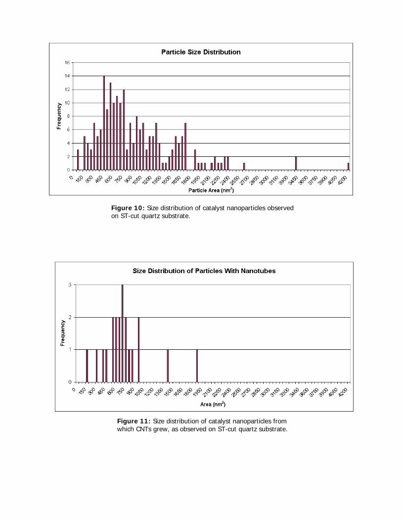
Figure 10: Size distribution of catalyst nanoparticles observed on ST-cut quartz substrate.
Figure 11: Size distribution of catalyst nanoparticles from which CNTs grew, as observed on ST-cut quartz substrate.

III. Ultra-low gas flow using Ruthenium Chloride and Iron(III) nitrate, nonahydrate, catalysts and 11nm alumina nanoparticles on SiO2/Si chips
The last experiment, which employed the ultra-low gas flow method
and used a liquefied mixture of Ruthenium Chloride, Iron(III) nitrate, nonahydrate, and 11nm-diameter alumina nanoparticles as catalysts on silicon chips, yielded the best CNTs. The most important goal was length, and the nanotubes produced by this method exceeded previous results in this respect. The longest CNT found is shown in Figure 12, which from end to end stretches for at least 804 microns (the upper end is ill-defined, so measurement is only approximate). If it were uncoiled into a straight line, it would certainly be longer than 1mm. The sample containing this nanotube was made by applying the liquid catalyst mixture by swiping the syringe across one edge of the chip to produce a thin streak of the mixture along the edge. That edge was then positioned so that it would be the first one over which gas flowed within the quartz tube. Long nanotubes such as this one could be found at the border of the catalyst zone, where the clean area of the chip began. Within the catalyst zone, there were catalyst particles and nanotubes densely packed and interwoven, so the nanotubes had no room to attain long length.
The CNTs found on this sample also showed alignment, the second goal of this project. The nanotube in Figure 12 follows a rather straight trajectory in its overall shape (disregarding the meanders and coils along the way), and this direction was parallel with the direction of gas flow. The same traits were also observed in many other long CNTs found within the transition zone between the catalyst-covered area and the uncovered silicon chip area, although there were also many exceptions. This marked the first time that significant alignment was observed in CNTs produced by the ultra-low gas flow method.
Figure 12: The longest CNT achieved during this project: 804 microns long. Ultra-low gas flow method was employed using a catalyst mixture consisting of Ruthenium Chloride, Iron(III) nitrate, nonahydrate, and alumina nanoparticles of 11nm diameter placed onto silicon chips.

Conclusions This project attempted to grow carbon nanotubes as long as possible, as aligned as possible, and as dense as possible. The best results were achieved using the Ruthenium Chloride, Iron(III) nitrate, nanohydrate, and alumina nanoparticle catalyst mixture under the ultra-low gas flow process. This combination of catalyst and CVD process yielded long nanotubes, the longest of which was over 800 microns, and many of the nanotubes exhibited alignment parallel to the gas flow. However, it remains a mystery why the ultra-low gas flow process was so problematic with the Iron(III), nanohydrate recipe that it consistently yielded CNTs in the early half of the research project and then abruptly stopped yielding any CNTs in the latter half. The other important result to investigate further is the shortcoming of the results on the ST-cut quartz compared to those reported by others – whether it truly has to do with the difference in catalysts or not. The last major point drawn from this study is the data supporting the prevailing theory that catalyst particles need to be of a certain size to prompt nanotube growth. Thus, it appears that researchers need to continue seeking ways to maximize the presence of appropriately sized particles. Acknowledgements I thank my mentors, Zhengtang Luo and Charlie Johnson for working with me and contributing to my project. I am grateful to NSF for funding this REU opportunity and to University of Pennsylvania for hosting it. I am also grateful to Jan Van der Spiegel for administering and assisting with the REU program.

References [1] Guest Editorial, “Who Should Be Given the Credit for the Discovery of Carbon
Nanotubes?,” CARBON, vol. 44, 2006, pp. 1621-1623. [2] C. See and A. Harris, “A Review of Carbon Nanotube Synthesis Via Fluidized-Bed
Chemical Vapor Deposition,” Ind. Eng. Chem. Res., vol. 46, 2007, pp. 997-1012. [3] J. Charlier, X. Blase, and S. Roche, “Electronic and Transport Properties of Nanotubes,”
Reviews of Modern Physics, vol. 79, May. 2007, pp. 677-711. [4] E. Drexler, “Nanotechnology,” AccessScience@McGraw-Hill;
http://www.accessscience.com. [5] Z. Jin et al., “Ultralow Feeding Gas Flow Guiding Growth of Large-Scale Horizontally
Aligned Single-Walled Carbon Nanotube Arrays,” Nano Letters, vol. 7, 2007, pp. 2073 - 2079.
[6] P.J.F. Harris, “Carbon Nanotubes,” AccessScience@McGraw-Hill;
http://www.accessscience.com. [7] D. Yuan et al., “Horizontally Aligned Single-Walled Carbon Nanotube on Quartz from a
Large Variety of Metal Catalysts,” Nano Letters, vol. xx, Jun. 2008. [8] M. Daenen et al., “The Wondrous World of Carbon Nanotubes,” Eindhoven University of
Technology, Feb. 2003.