giant plasmonic energy and momentum transfer on the nanoscale
TRANSCRIPT
Georgia State UniversityScholarWorks @ Georgia State University
Physics and Astronomy Dissertations Department of Physics and Astronomy
10-16-2009
Giant Plasmonic Energy and Momentum Transferon the NanoscaleMaxim DurachGeorgia State University
Follow this and additional works at: https://scholarworks.gsu.edu/phy_astr_diss
Part of the Astrophysics and Astronomy Commons, and the Physics Commons
This Dissertation is brought to you for free and open access by the Department of Physics and Astronomy at ScholarWorks @ Georgia State University.It has been accepted for inclusion in Physics and Astronomy Dissertations by an authorized administrator of ScholarWorks @ Georgia State University.For more information, please contact [email protected].
Recommended CitationDurach, Maxim, "Giant Plasmonic Energy and Momentum Transfer on the Nanoscale." Dissertation, Georgia State University, 2009.https://scholarworks.gsu.edu/phy_astr_diss/42
GIANT PLASMONIC ENERGY AND MOMENTUM TRANSFER ON THE NANOSCALE
by
MAXIM DURACH
Under the Direction of Dr. Mark I. Stockman
ABSTRACT
We have developed a general theory of the plasmonic enhancement of many-body
phenomena resulting in a closed expression for the surface plasmon-dressed Coulomb interaction.
It is shown that this interaction has a resonant nature. We have also demonstrated that
renormalized interaction is a long-ranged interaction whose intensity is considerably increased
compared to bare Coulomb interaction over the entire region near the plasmonic nanostructure.
We illustrate this theory by re-deriving the mirror charge potential near a metal sphere as well as
the quasistatic potential behind the so-called perfect lens at the surface plasmon (SP) frequency.
The dressed interaction for an important example of a metal–dielectric nanoshell is also
explicitly calculated and analyzed.

The renormalization and plasmonic enhancement of the Coulomb interaction is a
universal effect, which affects a wide range of many-body phenomena in the vicinity of metal
nanostructures: chemical reactions, scattering between charge carriers, exciton formation, Auger
recombination, carrier multiplication, etc. We have described the nanoplasmonic-enhanced
Förster resonant energy transfer (FRET) between quantum dots near a metal nanoshell. It is
shown that this process is very efficient near high-aspect-ratio nanoshells.
We have also obtained a general expression for the force exerted by an electromagnetic
field on an extended polarizable object. This expression is applicable to a wide range of
situations important for nanotechnology. Most importantly, this result is of fundamental
importance for processes involving interaction of nanoplasmonic fields with metal electrons.
Using the obtained expression for the force, we have described a giant surface-plasmon-
induced drag-effect rectification (SPIDER), which exists under conditions of the extreme
nanoplasmonic confinement. Under realistic conditions in nanowires, this giant SPIDER
generates rectified THz potential differences up to V10 and extremely strong electric fields up
to cmV1010 65 − . It can serve as a powerful nanoscale source of THz radiation. The giant
SPIDER opens up a new field of ultraintense THz nanooptics with wide potential applications in
nanotechnology and nanoscience, including microelectronics, nanoplasmonics, and biomedicine.
Additionally, the SPIDER is an ultrafast effect whose bandwidth for nanometric wires is 20 THz,
which allows for detection of femtosecond pulses on the nanoscale.
INDEX WORDS: Nanoplasmonics, Nanoplasmonic renormalization of Coulomb interaction, Surface-plasmon enhanced Förster energy transfer (FRET), Surface-plasmon-induced drag-effect rectification (SPIDER), Nanotechnology, Plasmonics on the nanoscale, Localized surface plasmons (LSPs), Surface plasmon polaritons (SPPs)

GIANT PLASMONIC ENERGY AND MOMENTUM TRANSFER ON THE NANOSCALE
by
MAXIM DURACH
A Dissertation Submitted in Partial Fulfillment of the Requirements for the Degree of
Doctor of Philosophy
in the College of Arts and Sciences
Georgia State University
2009

Copyright by Maxim Durach
2009

GIANT PLASMONIC ENERGY AND MOMENTUM TRANSFER ON THE NANOSCALE
by
MAXIM DURACH
Committee Chair: Dr. Mark Stockman
Committee: Dr. Vadym Apalkov
Dr. Nikolaus Dietz
Dr. Steven Manson
Dr. Unil Perera
Dr. Paul Wiita
Electronic Version Approved:
Office of Graduate Studies
College of Arts and Sciences
Georgia State University
December 2009

iv
Acknowledgements
First of all, I would like to express gratitude to my adviser Prof. Mark I. Stockman for
wonderful, interesting physics problems he proposed, for his guidance, advice and fruitful joint
work during the past three years.
I would like to thank the members of my committee, the Chair of the Department, Dr.
Richard Miller, and faculty members for enriching classes and a productive atmosphere.
I am thankful to my parents Anna and Eduard Duracz for encouraging me to go to
another hemisphere for education. Their daily support was felt across the Atlantic Ocean. Of
course, I would like to thank Anastasia Rusina for being with me all this time.

v
Table of Contents
Acknowledgements ...................................................................................................................... iv
List of Figures .............................................................................................................................. vii
List of Abbreviations .................................................................................................................... x
Chapter 1. Quasistatic Approximation and Surface Plasmons (SPs) ...................................... 1
1.1 Quasistatic Approximation ................................................................................................................ 1
1.2 Spectral Theory of SPs ...................................................................................................................... 6
Chapter 2. Nanoplasmonic Enhancement of Coulomb Interaction ....................................... 13
2.1 Quasistatic Interaction on the Nanoscale ....................................................................................... 13
2.2 Plasmonic Renormalization of Coulomb Interaction ..................................................................... 14
2.3 Examples of Nanoplasmonic Renormalization .............................................................................. 17
2.4 Giant Förster Energy Transfer near Metal-Dielectric Nanoshells ............................................... 25
2.5 General Properties of SP-Renormalized Quasistatic Interaction .................................................. 31
Chapter 3. Electromagnetic Retardation and Surface Plasmon Polaritons (SPPs) .............. 34
3.1 Retardation Effects .......................................................................................................................... 34
3.2 Radiative Decay of SPs .................................................................................................................... 36
3.3 SPPs at Planar Surfaces .................................................................................................................. 39
3.4 Excitation of SPPs ........................................................................................................................... 43
3.5 SPPs and SPs at Metal Nanowires .................................................................................................. 44

vi
Chapter 4. Forces in Electromagnetic Fields ........................................................................... 49
4.1 Introduction ..................................................................................................................................... 49
4.2 Electromagnetic Stress-Energy Tensor .......................................................................................... 51
4.3 Energy and Momentum Transfer in Electromagnetic Fields ........................................................ 53
4.4 Forces Acting on a Dipole in an Electromagnetic Field ................................................................ 54
4.5 Radiation Pressure in Macroscopic Bodies and the Photon Drag Effect ..................................... 56
4.6 Macroscopic Force Acting on Polarized Matter ............................................................................. 57
Chapter 5. Giant Surface Plasmon-Induced Drag Effect (SPIDEr) ...................................... 60
5.1 Introduction ..................................................................................................................................... 60
5.2 SPIDEr in Metal Nanowires ........................................................................................................... 62
5.3 SPIDEr as a THz Source ................................................................................................................. 66
5.4 SPIDEr as a Femtosecond SPP Detector ....................................................................................... 69
5.5 Conclusion ....................................................................................................................................... 71
References .................................................................................................................................... 72

vii
List of Figures
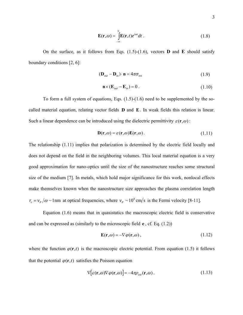
Figure 1.1. (color online) The skin-depth in silver (gray broken line) and
gold (golden solid line) as a function of frequency. Dielectric permittivities of
gold and silver were taken from experimental data [13]. ............................................ 5
Figure 2.1. (color online) Schematic of metal nanostructure and semiconductor nanocrystal
quantum dots (NQDs) situated in its vicinity. The metal nanostructure is
depicted by the dark blue color. Two electrons are indicated in NQDs by the
blue color and the local plasmonic fields are schematically shown by the orange
color. .......................................................................................................................... 15
Figure 2.2. (color online) Renormalization of Coulomb interaction between two charges in a
dielectric matrix with positioned at coordinates
near a metal-dielectric nanoshell. (a) The bare Coulomb interaction
(light violet) and renormalized interaction (orange). The
renormalized interaction is an order of magnitude larger than the Coulomb
interaction near the dipole plasmonic resonance. (b) Schematic of the
nanostructure. ............................................................................................................. 23
Figure 2.3. (color online) Renormalized (dressed) Coulomb interaction for a
silver nanoshell of aspect ratio . Point is fixed and indicated by the
black arrows in the upper parts of the panels. The dependence of on
is shown by color coding in the panels for the cross section of the
shell. The limits of this color coding are ; the maximum and higher
values of are depicted by red, and the minimum and lower values
of are shown by blue. Frequencies are indicated in the panels. ................. 24
Figure 2.4. (color online) Transfer and relaxation rates for NQDs at the outer surface of a
silver nanoshell, modified and enhanced by SPs. (a) Schematic of the system
and energy transfer processes. A nanoshell is indicated by a blue circle, and the
donor and acceptor NQDs are labeled by D and A, correspondingly. The
msl ε−= Re0D
2=dε nm22nm,3, ±=yx
1nm121 −= V
);,(Re ωrr ′W
9.0=x r′
),(Re rr ′W
, zx=r
mW± mW
WRe mW−
WRe ω

viii
frequency distributions of the transition oscillator strengths of the donor and
acceptor NQDs are shown by bold black curves. The energy transfer between
NQDs and subsequent relaxation are indicated by red arrows. (b)–(d) The
nonradiative and radiative relaxation rates (on logarithmic scale) for NQDs on
nanoshells for the aspect ratios specified in the panels. The FRET rate
(2.28) for two NQDs situated on the opposite poles of a nanoshell (cf. panel
(a)) is shown by the blue curves. The SP-mediated FRET rate averaged over the
position of the acceptor on the nanoshell (2.32) is shown by the light-blue
curves. The rate of transfer to the metal (2.33) is plotted in green. The
radiative rate (2.31) for a NQD at the surface of the nanoshell is depicted by
the red curves. ............................................................................................................ 29
Figure 3.1. (color online) Parameter for an SPP in silver nanowire in vacuum as a
function of frequency for exact solution of Eq. (3.37), when (red),
(green), (blue) and for quasi-static solution of Eq. (3.51)
(broken black curve). The quasi-static solution approximates exact solutions
with (see Figure 1.1) extremely well. ............................................. 48
Figure 5.1. (color online) Schematic of a SPIDEr in metal nanowire. Propagating SPPs
create forces acting on carriers in the nanowire, which leads to THz-band
voltage (emf) between the ends of the wire. Picosecond or femtosecond pulses
can be used to manipulate the time dependence of the created emf. ......................... 61
Figure 5.2. (color online) SPIDEr for quasi-monochromatic SPP pulses: emf and rectified
field dependence on the frequency and wire radius . Note the logarithmic
scale for the magtnitude of the effect. (a) Dependence of the SPIDEr emf per
unit SPP power on wire radius and frequency. The black broken curve
indicates the parameters at which SPP pressure is equal to striction. The
magnitude of the effect is denoted by the color-coding bar. (b) Dependence of
SPIDEr magnitude on wire radius per unit power of the SPP wave (solid
red curve). The contributions of the pressure and striction to the total magnitude
of SPIDEr are shown by the dashed curves. (c) Dependence of SPIDEr
abx =
Fγ
Fγ
mγ
rγ
kRx =
ωh nm5=R
nm10=R nm25=R
nm25≈<< slR
ωh R
cX
X R
ix
magnitude per unit power on frequency for . (d) Maximum
power that a wire can tolerate as a function of wire radius for different
frequencies . (e) The maximum SPIDEr rectified field (for the maximum
tolerable power ) as a function of frequency for three wire radii = 5, 30,
and 100 nm. (f) The maximum SPIDEr rectified field (for the maximum
tolerable power ) as a function of the wire radius for frequency
. ............................................................................................................ 68
Figure 5.3. (color online) SPIDEr created by ultrashort SPP pulses: fast femtosecond emf
response. (a) The dependence of the SPP lifetime on the frequency
for and . (b) The time dependence of the emf
(green line, left scale) and input power (red line, right scale). The pulse
duration is and the emf closely follows the SPP pulse
dynamics. (c) The same for much shorter pulse with . The pressure-
induced emf leads to a small broadening in the emf dynamics (green line). The
limiting exponential decay is outlined by the broken blue line. (d) Emf induced
by the short pulse in nanowire with with frequency .
The emf response is broadened, since , while . ........................ 70
cX ω nm5=R
mc R
ω mRE
mc R
mRE
mc R
eV55.1 =ωh
gpp vlt =
ωh nm5 =R nm30 =R )(tX
)(tc
fs30ps1 ≈>>= pt τ
fs40 =τ
nm30 =R eV2.1 =ωh
fs80 =τ fs150 =pt

x
List of Abbreviations
SP Surface plasmon
FRET Förster resonant energy transfer
SPIDER Surface-Plasmon-Induced Drag Effect Rectification
LSP Localized Surface Plasmon
SPP Surface Plasmon Polariton
THz Terahertz
NQD Nanocrystal Quantum Dot
SERS Surface Enhanced Raman Scattering
IR Infrared

1
Chapter 1. Quasistatic Approximation and Surface Plasmons (SPs)
1.1 Quasistatic Approximation
The Maxwell equations relate time and space derivatives of the electromagnetic field
with charges and currents. In many cases the time variation of fields is not fast enough, and
terms with temporal derivatives are overpowered by terms with spatial gradients. In such
situations electric and magnetic fields decouple and the electric field is determined only by the
charge density ),( trρ , while the magnetic field arises from currents. Two equations describing
the local (microscopic) electric field ),( tre under these circumstances are [1-3]:
),(4),( tt rre πρ=⋅∇ , (1.1)
0),( =×∇ tre . (1.2)
Finding a solution of microscopic equations (1.1) and (1.2) is possible for individual
atoms or molecules, but is an extremely complicated many-body problem even for a nanoscopic
particle consisting of several atoms. Not only is it very time-consuming to solve microscopic
equations (1.1) and (1.2) numerically, it is hard to analyze such a solution or compare it to an
experiment, since it contains too many initial parameters, e.g. atomic coordinates, velocities etc.
It is much more approachable to obtain a spatially averaged macroscopic field eE = . It differs
from the exact microscopic solution ),( tre by sharp spatial and temporal field fluctuations
)( Eee −=∆ connected with the microscopic composition and dynamics of matter. In the
overwhelming majority of practical situations it is enough to know the average macroscopic field
2
in order to explain the optical phenomena on the macroscale. Nevertheless, fluctuations have
been shown to be important on the nanoscale in the studies of non-linear optical effects in rough
or fractal metal composites [4, 5]. In this work we will focus on the effects of the average
(macroscopic) field, assuming that structures we consider are homogeneous and have smooth
enough surfaces to avoid large contributions from fluctuations.
In the charged systems the macroscopic average of the charge density from Eq. (1.1) can
be represented using the polarization vector P :
P⋅∇−= extρρ , (1.3)
where only so-called external charges extρ contribute to the total macroscopic charge of a
structure [6]. The polarization vector also determines macroscopic surface charge density
)ˆ( nP ⋅=− extσσ . (1.4)
on the surface of a polarized object, with normal ort n pointing outward. Here extσ is the surface
density of the external charges.
Using Eqs. (1.1)-(1.4), one is able to obtain the equations describing macroscopic
electrostatic fields
)(4)( rrD extπρ=⋅∇ , (1.5)
0)( =×∇ rE , (1.6)
where the electric induction vector PED π4+= was introduced. It is easy to notice that Eqs.
(1.5)-(1.6) hold not only for time-dependent vector fields ),( trD and ),( trE , but also for their
temporal Fourier amplitudes defined by
∫∞
∞−
= dtet tiωω ),(),( rDrD , (1.7)
3
∫∞
∞−
= dtet tiωω ),(),( rErE . (1.8)
On the surface, as it follows from Eqs. (1.5)-(1.6), vectors D and E should satisfy
boundary conditions [2, 6]:
extinout πσ4)( =⋅− nDD (1.9)
0)( =−× inout EEn . (1.10)
To form a full system of equations, Eqs. (1.5)-(1.6) need to be supplemented by the so-
called material equation, relating vector fields and . In weak fields this relation is linear.
Such a linear dependence can be introduced using the dielectric permittivity ),( ωε r :
),(),(),( ωωεω rErrD = . (1.11)
The relationship (1.11) implies that polarization is determined by the electric field locally and
does not depend on the field in the neighboring volumes. This local material equation is a very
good approximation for nano-optics until the size of the nanostructure reaches some structural
size of the medium [7]. In metals, which hold major significance for this work, nonlocal effects
make themselves known when the nanostructure size approaches the plasma correlation length
nm1~ ωFc vr = at optical frequencies, where scm10~ 8Fv is the Fermi velocity [8-11].
Equation (1.6) means that in quasistatics the macroscopic electric field is conservative
and can be expressed as (similarly to the microscopic field e , cf. Eq. (1.2))
),(),( ωϕω rrE −∇= , (1.12)
where the function ),( trϕ is the macroscopic electric potential. From equation (1.5) it follows
that the potential satisfies the Poisson equation
[ ] ),(4),(),( ωπρωϕωε rrr ext−=∇∇ . (1.13)
D E
),( trϕ
4
The boundary conditions (1.9)-(1.10) can be formulated in terms of potentials:
extin
inout
out nnπσϕεϕε 4−=
∂∂
−∂∂ (1.14)
inout ϕϕ = . (1.15)
Equations (1.13), (1.14) and (1.15) describe quasistatic phenomena. As was mentioned
above, these equations are true if the terms in the Maxwell equations with spatial derivatives of
the field dominate over the terms with temporal derivatives, corresponding to an estimate
LcT>=
π20D , (1.16)
where c is the speed of light, 0D is the field reduced wavelength in vacuum, T and L are the
period of the field oscillations and the characteristic length in the problem, correspondingly.
Nanooptic problems deal with structures which are enclosed within lengths nm50~ L and fields
that change dramatically on this spatial scale. This means that the quasi-static approximation is
suitable to describe fields with periods fs1 >T or frequencies eV4 <ωh . This covers the whole
optical range and below. In other words, the highest frequency in the problem determines the
volumes within which the near-field may be described by a quasistatic approximation.
In metals below the plasma frequency - basic nanoplasmonic materials - the magnetic
field is enhanced by the larger prefactor in the displacement current (see Eq. (3.4)). This
prefactor is inversely proportional to the skin depth
)(Re0 ωε msl −≈ D , (1.17)
where )(ωε m is the metal dielectric function (for specific definitions of skin depth for different
types of waves see Sect. 3.3) [3, 6, 12]. The quasistatic approximation requires the ability to
neglect the magnetic term in the Maxwell-Faraday equation (see Eq. (3.2)), which
5
correspondingly becomes more demanding in plasmonic metals. Inside metal inclusions the
relationship (1.16) is supplemented by
sinc lL < . (1.18)
This means that the characteristic size incL of metal inclusions of the structure studied
using quasistatic approximation cannot exceed the skin depth. The dependence of the skin depth
in silver and gold as a function of frequency at optical frequencies is shown in Figure 1.1.
Unfortunately, since the scale on which quasistatics is valid does not extend further than
0D , we are unable to describe the far-zone behavior of the field, leaving scattering and radiation
by plasmonic nanostructures out of the scope of quasistatics (see Sect. 3.2). However,
quasistatics describes most near-field effects extremely well.
Figure 1.1. (color online) The skin-depth in silver (gray broken line) and gold (golden solid line) as a function of frequency. Dielectric permittivities of gold and silver were taken from experimental data [13].
msl ε−= Re0D
6
1.2 Spectral Theory of SPs
The general theory based on the quasistatic equation (1.13) in electrically neutral two-
component systems ( 0=extρ ) originated from attempts to describe the percolation threshold in
metal-dielectric composites [14, 15]. It was further developed and used in papers devoted to the
studies of Anderson localization of surface plasmons [16], coherent control of optical fields in
metal nanostructures [17, 18], surface enhanced Raman scattering (SERS) [19], surface plasmon
amplification by stimulated emission of radiation (SPASER) [20, 21]. Following these references,
we will describe in this Section the formulas of nanoplasmonic spectral theory required for
present work.
Consider a two-component structure consisting of a dielectric host with metal inclusions,
whose dielectric function can be written as
))()((),( dmd εωεεωε −Θ+= rr , (1.19)
where dε and )(ωεm are bulk dielectric functions of dielectric and metal correspondingly, and
)(rΘ is the function characterizing geometry of the structure, which is equal to 1 if r is inside
the metal, and 0 otherwise.
The structure is surrounded by the surface S (which encloses volume V), so that
0)( =Θ∈Sr
r and 0)( =Θ∇∈Sr
r . The structure is excited by the external field with potential
)(0 rϕ , which satisfies the Laplace equation within the surface S
0)(02 =∇ rϕ . (1.20)
The total potential can be represented as
)()()( 10 rrr ϕϕϕ += , (1.21)

7
where )(1 rϕ is the induced potential, satisfying homogeneous Dirichlet or Neumann conditions
at the surface S
( ) ,0)()(ˆ)( 11 =∇⋅∈Sr
rrnr ϕϕ (1.22)
where )(ˆ rn is a normal ort to surface S at a point r .
With dielectric function (1.19) the operator from Eq. (1.13) becomes
( ) ( ) ( ) 2)()()(),( ∇−∇Θ∇−=∇∇ ωεωεωε sdm rr , (1.23)
where [ ] 1)(1)( −−= dms εωεω is the so-called spectral parameter, which contains all the
information about the materials. Substituting potential (1.21) into Eq. (1.13) with 0=extρ and
using Eqs. (1.19) and (1.20) one obtains
( ) ( ))()()()()()( 012
1 rrrrr ϕϕωϕ ∇Θ−∇=∇−∇Θ∇ s . (1.24)
To solve Eq. (1.24) one needs to introduce an eigenproblem
( ) 0)()()( 2 =∇−∇Θ∇ rrr nnn s ϕϕ , (1.25)
where ns are the eigenvalues, corresponding to eigenfunctions )(rnϕ , which satisfy boundary
condition (1.22). Eigenfunctions, , and eigenvalues, ns , for several geometries are
presented in Sect. 2.3.
Multiplying Eq. (1.25) by the complex-conjugate eigenfunction )(* rmϕ and integrating
over the volume V, we obtain
0)()()()()( ** =∇⋅∇+∇⋅∇Θ− ∫∫V
nmnV
nm dVsdV rrrrr ϕϕϕϕ . (1.26)
In Eq. (1.26) the surface integrals vanished, since the eigenfunctions satisfy Eq. (1.22) and
. Setting nm = in Eq. (1.26) one obtains an expression for eigenvalues
)(rnϕ
0)( =Θ∈Sr
r

8
∫
∫∇
∇Θ=
Vn
Vn
ndV
dVs 2
2
)(
)()(
r
rr
ϕ
ϕ.
(1.27)
Eq. (1.27) shows that the eigenvalue represents the fraction of the eigenmode energy that
penetrates the metal constituent of the nanostructure. This implies that are real numbers
between 0 to 1.
Equation (1.25) does not contain frequency or any information about materials and it is
determined only by the geometry of nanostructure. Eigenfunctions describe fields of the
so-called localized surface plasmons (LSP) – electrostatic modes, which have been studied
recently in connection with several important nanoscale effects and applications [17, 19-26].
The complex frequencies nnn iγω −=Ω of LSPs can be found as
nnn sis =− )( γω . (1.28)
If the so-called SP resonance quality factor
nnnQ γω= (1.29)
is high, 1>>nQ , then one can use a Taylor series to expand ≈− )( nn is γω
...)()( +∂∂−= n
sis nn ωωωωγω , which gives the following expressions for the resonance
frequency nω and spectral width nγ [19, 20, 27]:
nn ss =)(Re ω . (1.30)
nm
m
n
nst s
s
ωωωωε
ωεωω
γ=
∂∂=
′=
)(Re)(Im
)()(Im
, where n
ss nωωω
ωω=∂
∂=′ )(Re)( .
(1.31)
Note that, as follows from Eq. (1.31), the SP linewidth (relaxation rate) )(ωγ does not
depend on the geometry of the nanostructure and is a function of only frequency. The relaxation
ns
ns
)(rnϕ
9
rate )(ωγ , related to the SP dephasing time as ))(2(1)( ωγωτ = , is extremely important in
plasmonics and determines the scale of temporal evolution of plasmonic fields, which is
fs100~ τ (see also Sect. 5.4). The SP dephasing times determine the ability of SPASER to
generate and amplify local fields [20, 21] as well as the local field enhancement
20 ωτ=∝QEE , where E is the local field and 0E is the field of the external excitation [28,
29]. This enhancement is especially important for nonlinear processes, for example SERS, whose
enhancement factor is 40EEg R ∝ [19].
The relaxation time τ may not be determined only by the metal dielectric function [see
Eq. (1.31)]. It is additionally influenced by non-local effects for small metal nanoparticles with
radii nm52−≈≤ ωFvR [8, 9, 11], and by radiative decay for large nanoparticles [29-32]. The
quasistatic approximation is invalid for nm25≈≥ slR , but the expression for the relaxation rate
(1.31) may be unaffected by radiative decay even for radii larger than sl , as is shown in Sect. 3.2.
Turning back to spectral theory, let us exchange m and n and complex-conjugate Eq.
(1.26); subtracting the result from Eq. (1.26) we obtain the orthogonality relation between the
eigenmodes
0)()()( * =∇⋅∇⋅− ∫V
nmmn dVss rr ϕϕ . (1.32)
It follows from Eq. (1.32) that scalar product of the eigenproblem can be selected as
∫ ∇⋅∇=V
dV)()()( 1*221 rr φφφφ . (1.33)
Expression (1.33) satisfies all necessary requirements of the scalar product [19]. The
eigenfunctions are orthogonal with respect to the scalar product (1.33) and can be normalized as
10
mnmn δϕϕ =)( . (1.34)
Consider the retarded Green’s function );,( ωrr ′G of the problem given by Eq. (1.24).
The Green’s function );,( ωrr ′G should satisfy the following equation
( ) )();,()()( 2 rrrrr ′−=′∇−∇Θ∇ δωω Gs , (1.35)
as well as the boundary conditions (1.22). It can be expanded over the eigenfunctions in
the form
∑ ′=′n
nnaG )();();,( rrrr ϕωω . (1.36)
Substituting expression (1.36) into Eq. (1.35), multiplying by )(* rmϕ and integrating over
V, we obtain )())()(;( * rr ′=−′ mmm ssa ϕωω and, correspondingly, for the Green’s function [19]
∑ −′
=′n n
nn
ssG
)()()();,(
*
ωϕϕω rrrr .
(1.37)
Two features of expansion (1.37) are important [19]. First, it separates the dependencies
on geometry and material properties. The geometrical properties of the nanosystem enter only
through the eigenfunctions and eigenvalues which are independent of the material
properties. Therefore they can be computed for a given geometry only once, which simplifies
and accelerates further computations. Complementarily, the material properties of the system are
present in Eq. (1.37) only through a single function: the spectral parameter )(ωs . The second
important feature of Eq. (1.37) is that this Green’s function satisfies exact analytical properties
due to the form of Eq. (1.37) that contains only simple poles in the lower half-plane of the
complex frequency ω and does not have any singularities in the upper half-plane of ω .
Consequently, G is a retarded Green’s function that automatically guarantees the causality of
)(rnϕ
)(rnϕ ns
11
the results of time-dependent calculations. Namely, the Green’s function in the time domain
satisfies the condition 0);,( =′ tG rr for 0<t .
The induced potential )(1 rϕ in the nanostructure can be expressed through Green’s
function (1.37) [19]
rdGV
′⎟⎠⎞
⎜⎝⎛
′∂′∂′Θ
′∂∂′−= ∫ 30
1)()();,()(
rrr
rrrr ϕωϕ ,
(1.38)
where ∇≡∂∂ r . Correspondingly, the total potential (1.21) assumes the form
rdGV
′⎟⎠⎞
⎜⎝⎛
′∂′∂′Θ
′∂∂′−= ∫ 30
0)()();,()()(
rrr
rrrrr ϕωϕϕ ,
(1.39)
Integrating this relation by parts twice and using we get
rdGV
′⎟⎠⎞
⎜⎝⎛ ′
′∂∂′Θ
′∂∂′−= ∫ 3
00 );,()()()()( ωϕϕϕ rrr
rr
rrr , (1.40)
Relation (1.12) allows one to obtain the closed expression for the total optical field )(rE
in terms of the excitation field )(0 rE
rdEGEEV
′′′Θ′+= ∫ 300 )()();,()()( rrrrrr βαβαα ω , (1.41)
where the dyadic Green’s function is [19]
);,();,(2
ωωβα
αβ rrrr ′′∂∂
∂=′ G
rrG ,
(1.42)
Now let us substitute the expansion (1.37) into Eq. (1.40)
rdss
n
Vn n
n ′⎟⎟⎠
⎞⎜⎜⎝
⎛′∂′∂′Θ
′∂∂′⋅
−−= ∫∑ 3
*
00)()()(
)()()()(
rrr
rrrrr ϕϕ
ωϕϕϕ ,
(1.43)
and using eigenproblem (1.25) we obtain [19]
0)( =Θ∈Sr
r
12
rdss
s n
Vnn
n
n ′′∂′∂′⋅
−−= ∫∑ 3
2
*2
00)()()(
)()()(
rrrrrr ϕϕϕ
ωϕϕ ,
(1.44)
This expression can be rewritten in the form
rdGV
′′′∂
∂′−= ∫ 32
2
00 );,()()()( ωϕϕϕ rrr
rrr , (1.45)
where );,( ωrr ′G is another retarded Green’s function [19]
∑ ′−
=′n
nnn
n
sssG )()()(
);,( * rrrr ϕϕω
ω . (1.46)
It is shown in the next Chapter [see Eq. (2.7)] that the Green’s function (1.46) determines
the renormalization of a quasistatic interaction in the vicinity of metal nanostructures.

13
Chapter 2. Nanoplasmonic Enhancement of Coulomb Interaction
2.1 Quasistatic Interaction on the Nanoscale
Nanostructured plasmonic metal systems are known to enhance greatly a variety of
radiative and non-radiative optical processes, both linear and nonlinear, which are due to the
interaction of an electron in a molecule or semiconductor with the enhanced local optical field of
the surface plasmons (SPs). Among them are surface-enhanced Raman scattering (SERS) [19,
33-37], SP-enhanced fluorescence [38-42], fluorescence quenching in the proximity of metal
surfaces [38, 41, 43], coherent anti-Stokes Raman scattering (CARS) [44], surface-enhanced
hyper-Raman scattering (SEHRS) [45], etc. These are distinctly different from numerous many-
body phenomena that are due to the Coulomb interaction between charged particles: carriers
(electrons and holes) and ions. These include carrier–carrier or carrier–ion scattering, energy and
momentum transfer (including the drag effect), thermal equilibration, exciton formation, impact
ionization and Auger effects [15].
It is not widely recognized that these and other many-body effects can also be modified
and enhanced by the SP local fields. A special but extremely important class of such many-body
phenomena is constituted by chemical reactions at metal surfaces, including catalytic reactions.
In the paper [46] we have proposed a general and powerful theory of the plasmonic enhancement
of the many-body phenomena resulting in a closed expression for the SP-dressed Coulomb
interaction. Metal-dielectric nanoshells are extremely important for modern nanotechnology [47].
We illustrate our theory by computing the dressed interaction explicitly for metal-dielectric

14
nanoshells, which exhibits a rich resonant behavior in both the magnitude and phase. This
interaction is used to describe the nanoplasmonic-enhanced Förster resonant energy transfer
(FRET) between nanocrystal quantum dots (NQDs) in proximity to a plasmonic nanoshell. This
is of great interest for plasmonic-enhanced solar cells and light-emitting devices [48]. Catalysis
at nanostructured metal surfaces, nonlocal carrier scattering, and SERS are discussed in this
thesis among other effects and applications where the nanoplasmonic renormalization of the
Coulomb interaction may be of principal importance.
2.2 Plasmonic Renormalization of Coulomb Interaction
Consider a system of charged particles situated in the vicinity of a plasmonic metal
nanosystem. For definiteness, we will assume that these particles are electrons, although they can
also be holes or ions of the lattice. One of the examples of such systems is a semiconductor in
proximity to a nanostructured metal surface. When an electron undergoes a transition with some
frequency ω , this transition is accompanied by local electric fields oscillating with the same
frequency. These fields excite SP modes with the corresponding frequencies whose fields
overlap in space with the transition fields. A property of these SP eigenmodes is that they can be
delocalized over the entire nanostructure [16]. The local optical fields of the SPs can excite a
resonant transition of another electron. This process, which in the quantum mechanical language
is the electron–electron interaction by the exchange of an SP quantum, renormalizes (‘dresses’)
the direct interaction between these two charges. As a result, the direct (‘bare’) Coulomb
interaction between the electrons, ( )rrrr ′−=′− dV ε1)( , where dε is the dielectric constant of
the embedding medium, is replaced by the dressed interaction );,( ωrr ′W . This dressed
interaction is generally not translationally invariant, i.e., it depends on the coordinates r and r′

15
of both electrons; it also depends on the transition frequency . Note that W is generally a
complex function, and its phase describes a delay inherent in the plasmonic reaction. This phase
varies sharply across plasmonic resonances, as we will show later in this paper.
We schematically illustrate this SP-mediated electron–electron interaction in Figure 2.1,
where we show electrons in two semiconductor NQDs situated at the surface of a metal
nanostructure. The plasmonic fields, indicated by orange, excited by one of the electrons interact
with the other one in a different NQD. The interacting charges could also belong to the same
quantum dot and could be not only electrons but also holes.
Figure 2.1. (color online) Schematic of metal nanostructure and semiconductor nanocrystal quantum dots (NQDs) situated in its vicinity. The metal nanostructure is depicted by the dark blue color. Two electrons are indicated in NQDs by the blue color and the local plasmonic fields are schematically shown by the orange color.
The resonant nature of the electron-plasmon interaction may lead to the significant
enhancement of the dressed interaction W with respect to the bare one, V. A typical SP
eigenmode tends to form ‘hot spots’ of the local fields separated by distances on the order of the
size of the entire plasmonic nanostructure [16]. Therefore one should expect that the dressed
interaction will also be delocalized over such distances, i.e., be relatively much more long-
ranged than the bare Coulomb interaction.
ω

16
The dressed interaction );,( ωrr ′W , by definition, is the potential created at a point r by
a charge positioned at another point r′ and oscillating with frequency . We assume that the
size of the system is much smaller than any relevant electromagnetic length (radiation
wavelength, skin depth, etc) and will use the quasistatic approximation, which is conventional in
nanoplasmonics. In this case, W satisfies the continuity equation
)(4);,(),( rrrrr
rr
′−−=⎥⎦⎤
⎢⎣⎡ ′
∂∂
∂∂ πδωωε W ,
(2.1)
where the dielectric function ),( ωε r is given by Eq. (1.19).
Now let us represent the W as a sum of the ‘bare’ Coulomb potential V and the additional
interaction R due to the nanostructure
);,()();,( ωω rrrrrr ′+′−=′ RVW . (2.2)
With dielectric permittivity in the explicit form (1.19) Eq. (2.1) reads
)(4);,()()(
1);,(2
2
rrrrr
rr
rrr
′−−=⎥⎦⎤
⎢⎣⎡ ′
∂∂
Θ∂∂
−′∂∂ δ
επω
ωω
d
Ws
W . (2.3)
Using Eq. (2.3) and the fact that
)(4)(2
2
rrrrr
′−−=′−∂∂ δ
επ
d
V , (2.4)
we obtain
⎥⎦⎤
⎢⎣⎡ ′−
∂∂
Θ∂∂
−=′∂∂
−⎥⎦⎤
⎢⎣⎡ ′
∂∂
Θ∂∂ )()();,()();,()( 2
2
rrr
rr
rrr
rrr
rr
VRsR ωωω . (2.5)
Eq. (2.5) is similar to Eq. (1.24). Therefore, W can be written by analogy with Eq. (1.45)
rdGVVWV
′′′′′′∂
∂′−′′−′−=′ ∫ 32
2
);,()()();,( ωω rrr
rrrrrr , (2.6)
where is the Green’s function given by (1.46).
ω
);,( ωrr ′G

17
If the system is in an infinite space (or the boundaries are remote enough), then the use of
Green’s identity in Eq. (2.6) simplifies it to the form [46]
.)()()(
41
);,(4)();,(
*∑ ′−
+′−
=
=′+′−=′
nnn
n
n
d
d
sss
GVW
rrrr
rrrrrr
ϕϕωε
π
ωεπω
(2.7)
This is a simple, yet general and powerful result: the Coulomb interaction is renormalized
by the full retarded Green’s function (1.46) whose contraction also describes the nanoplasmonic
enhancement of SERS and other optical phenomena. The poles of the Green’s function (1.46)
correspond to the SP modes whose frequencies nω are given by the equation nn ss =)(ω . Close to
such frequencies, G becomes large, proportional to the quality factor nQ of the SP resonance
[19]. This describes the plasmonic renormalization and enhancement of the dressed Coulomb
interaction.
2.3 Examples of Nanoplasmonic Renormalization
We will illustrate the plasmonic renormalization and enhancement of the Coulomb
interaction near several nanoplasmonic systems. Let us start with metal nanoshell. Such
nanoshells have significant fundamental and applied interest [47]. Eigenfunctions for nanoshells
are products of the radial power functions and spherical harmonics that describe the angular
dependence )ˆ()( rlmllm YrR±± =ϕ . We express the radial functions in the following form
( )⎪⎩
⎪⎨
⎧
><<+
<
+=
+
+±±
±±
±
arraarbraCarB
brarA
alf
rRl
ll
ll
ll
ll
if,)( if ,)()(
if ,)(
)12()(
1
1
,
(2.8)
where b is the inner and a is the outer radius of the nanoshell, and ±lf are normalization factors.
18
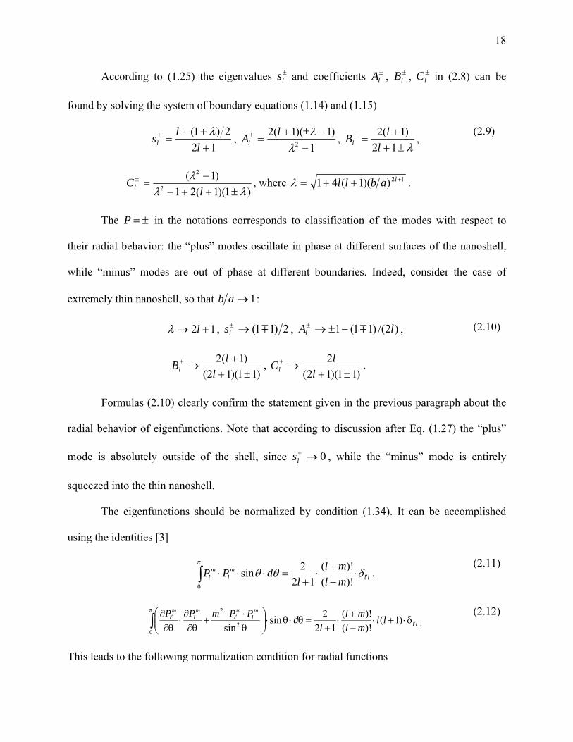
According to (1.25) the eigenvalues ±ls and coefficients ±
lA , ±lB , ±
lC in (2.8) can be
found by solving the system of boundary equations (1.14) and (1.15)
122)1(
++
=±
llsl
λm,
1)1)(1(2
2 −−±+
=±
λλlAl ,
λ±++
=±
12)1(2
llBl ,
)1)(1(21)1(
2
2
λλλ
±++−−
=±
lCl , where 12))(1(41 +++= labllλ .
(2.9)
The ±=P in the notations corresponds to classification of the modes with respect to
their radial behavior: the “plus” modes oscillate in phase at different surfaces of the nanoshell,
while “minus” modes are out of phase at different boundaries. Indeed, consider the case of
extremely thin nanoshell, so that 1→ab :
12 +→ lλ , 2)11( m→±ls , )2/()11(1 lAl m−±→± ,
)11)(12()1(2±+
+→±
llBl ,
)11)(12(2
±+→±
llCl .
(2.10)
Formulas (2.10) clearly confirm the statement given in the previous paragraph about the
radial behavior of eigenfunctions. Note that according to discussion after Eq. (1.27) the “plus”
mode is absolutely outside of the shell, since 0→+ls , while the “minus” mode is entirely
squeezed into the thin nanoshell.
The eigenfunctions should be normalized by condition (1.34). It can be accomplished
using the identities [3]
llm
lm
l mlml
ldPP ′′ ⋅
−+
⋅+
=⋅⋅⋅∫ δθθπ
)!()!(
122sin
0
. (2.11)
ll
ml
ml
ml
ml ll
mlml
ldPPmPP
′
π′′ δ⋅+⋅
−+
⋅+
=θ⋅θ⋅⎟⎟⎠
⎞⎜⎜⎝
⎛θ⋅⋅
+θ∂
∂⋅
θ∂∂
∫ )1()!()!(
122sin
sin02
2
. (2.12)
This leads to the following normalization condition for radial functions

19
mmllPPmmllPl
PlP
lmPml R
rll
rRd ′′′′′′′ =⋅
⎪⎭
⎪⎬⎫
⎪⎩
⎪⎨⎧
⋅+
+⎟⎟⎠
⎞⎜⎜⎝
⎛∂∂
=Ω⋅∇⋅∇∫ δδδδδϕϕ 2
2
2)1( .
(2.13)
From (2.13) we have calculated the normalization factors in (2.8):
)1(4)12)(1(
+±++±
±=±
llfl λ
λλ . (2.14)
Now let us study a very significant example of a nanosphere. In this case only the +=P
mode represents physically sensible solution, whose eigenvalues for nanosphere are
)12( += llsl . The radial function is in this case
⎩⎨⎧
><
+=+
−−
arrabrar
alRl
l
l if )( if ,)(
)12(1
2/12/1 . (2.15)
Therefore, the renormalized Coulomb interaction (2.7) near the metal nanosphere is
)()()/(
)/)(/()12/()(
)12/(4)();,( *12
2
rrrrrr ′⋅⎟⎟⎠
⎞⎜⎜⎝
⎛′′
+−+
+′−=′ ∑ + lmlmlm
l
l
d
YYrra
rrralls
lla
VWωε
πω , (2.16)
where ar > is the radius of the source and r′ is the potential observation point. The upper value
is for ar <′ , and the lower for ar >′ . At 0→ω the metal dielectric function diverges, therefore
0)0( →s . This simplifies Eq. (2.16) at to
,)/(
)/(1
)()()12(
14)();,(
22
*12
rrrr
rrrrrr
′′−⋅
′−
′−=
=′⋅⎟⎟⎠
⎞⎜⎜⎝
⎛′+
−′−=′ ∑+
rara
YYrr
ala
VW
dd
lmlmlm
l
d
εε
επω
(2.17)
The last part of Eq. (2.17) is the Green's function of the Poisson equation for a Dirichlet problem
which can be also obtained through the method of mirror charges [2, 6].
In general, formula (2.7) in the limit 0)( →ωs gives the expression for static interaction
in the vicinity of a perfect conductor
ar >′

20
∑ ′−′−
=′n
nndd
W )()(41);,( * rrrr
rr ϕϕεπ
εω .
(2.18)
Another interesting situation occurs when considering a thin metal film embedded into a
dielectric. The eigenfunctions in cylindrical coordinates have the form φρϕ immkkm ekJzg )()(±± = ,
where axis z is orthogonal to the film and the film is in the 2/dz ≤ region. If the dielectric on
both sides of the film is the same, the eigenstates are even or odd with respect to transformation
zz −→ and denoted with “+” or “-”, correspondingly. The behavior of eigenstates in
perpendicular to the film direction is described by
⎪⎩
⎪⎨
⎧
><
−<±=
−−±±
+
±±
2/ if 2/ if ,)2/(tr)(tr
2/ if ,
)2/(
)2/(
dzedzkdkz
dzefg
dzk
dzk
kk , where coshtr =+ , sinhtr =−
(2.19)
Boundary conditions (1.14)-(1.15) give the following eigenvalues
)1(21 kd
k es −± = m . (2.20)
Normalization of eigenfunctions ±kmϕ can be achieved using the formula
)(
)(12)2/(tr)2/(tr12)( *
kk
kkkkd
kdkfdzdd
mmPP
mmPPkPmk
Pkm
′−=
=′−⋅⎟⎟⎠
⎞⎜⎜⎝
⎛+⋅=
′′
′′±
±′′′∫δδδ
δπδδφρρϕϕ m
,
(2.21)
so that
))2/tanh(1(41
kdfk +
=+
π and
))2/coth(1(41
kdfk +
=−
π. (2.22)
Now let us consider a point source at 2/2/ dhdz >+= and see what is the potential at
the other side of the film at the frequency of plasmon resonance of a flat surface, i.e. when
dspm εωε −=)( or 2/1)( =sps ω .

21
.)1(4
)(4
)2/(
1
))2/tanh(1()1(
))2/coth(1()1(
4)(4
)2/(
1);2/,2/(
0
22/)(0
22
0
)2/()2/(0
22
∫
∫∞
−′−−
∞ +′
−
−+′
−
−−
+−′
+−−′+′
=
=⎟⎟⎠
⎞⎜⎜⎝
⎛+
−+
++′
+
+−−′+′
==−<′+=
kdkdzhk
dd
dzk
kd
kddzk
kd
kdkh
d
d
sp
eeekJ
dkdhz
kde
ee
kde
eee
kJdk
dhzdzdhzW
πρ
επ
ρε
πρ
επ
ρεωω
(2.23)
Using the relation ∫∞
−⋅=+0
022 )(1 ρρ kJedkz kz [49], we arrive at
.)2/3(
1);2/3,2/(22 zdh
dhzdhzWd
sp′−−+′
==−<′+=ρε
ωω (2.24)
Formula (2.24) implies, that an ideal three-dimensional image of the source charge is formed
behind the film at distance hd − from the film [8]. This shows that the theory of the
renormalized Coulomb interaction can be used for further studies of imaging by metal
nanostructures.
Let us turn back to metal nanoshell. Using (2.8) and (2.9) we have obtained [46] the
renormalized Coulomb potential );,( ωrr ′W for arr >′, , where a is the external radius of the
nanoshell, to be [46]
∑ ′⎟⎟⎠
⎞⎜⎜⎝
⎛′+
+′−=′+
lmlmlm
l
l
d
YYrr
alxF
aVW )()(
12),(4)();,( *
12
rrrrrr ωεπω .
(2.25)
Analogous expressions for the r and/or r′ belonging to the inner part of the shell also
have been obtained and used in the computations, in particular, those illustrated in Figure 2.3. In
(2.25), the spherical harmonics lmY depend only on the directions of the corresponding vectors,
and x is the shell aspect ratio (i.e. the ratio of the inner to outer shell radius). The form factor lF
is given by an exact resonant pole expression:

22
−
−−
+
++
−+
−=
l
ll
l
lll ss
fsss
fsxF)()(
),(ωω
ω , (2.26)
where P = ± refers to the symmetry of the corresponding SP mode, eigenvalues ±ls are given in
(2.9) and normalization factors ±lf are given by Eq. (2.14).
Note that SP eigenmodes with the P = + symmetry have dominating oscillator strength in
the long-wavelength (red and near-IR) part of the spectrum, where the quality factors of the SP
resonances for noble metals are high, and which are most important in many cases.
We demonstrate the renormalization of the Coulomb interaction near thin metal-dielectric
nanoshell with radius nm20 =a and aspect ratio 9.0=x in Figure 2.2. Two charges in a
dielectric matrix with 2=dε are separated by the distance nm6 and placed at positions with
radii nm22 =′= rr . The renormalized interaction (orange curve in Figure 2.2(a)) is several
times larger in magnitude than the bare Coulomb interaction 1nm121 −= V (light violet curve in
Figure 2.2(a)) and is extremely large at the dipole SP resonance, with 1nm1 −≈ W . Note the
change of phase of the interaction at the SP resonances, where screening is substituted by anti-
screening.
We depict the resonant behavior and renormalization (enhancement) of the Coulomb
interaction in Figure 2.3 for a silver nanoshell with aspect ratio x = 0.9 deposited on a dielectric
core with permittivity 2=dε embedded into a host with the same permittivity. The silver
dielectric function is adopted from the experimental data [13]. For this specific nanoshell, the
lowest dipole eigenmode (quantum numbers L = 1, P = −) has eigenfrequency 60.11 =−ωh eV.
For a red-detuned (from the dipole SP resonance) electronic transition frequency 5.1=ωh eV,
the renormalized interaction is displayed in Figure 2.3 (a). Very close to the singular point rr ′= ,

23
Figure 2.2. (color online) Renormalization of Coulomb interaction between two charges in a dielectric matrix with positioned at coordinates near a metal-dielectric
nanoshell. (a) The bare Coulomb interaction (light violet) and renormalized interaction (orange). The renormalized interaction is an order of magnitude larger than the Coulomb interaction near the dipole plasmonic resonance. (b) Schematic of the nanostructure.
the renormalization is reduced to conventional dielectric screening: this is displayed by the
opposite sign (blue color in the panel) of with respect to the bare Coulomb
potential (the red dot pointed to by the arrow). On the opposite side of the nanosphere, there is a
‘mirror image’ of the dressed interaction potential ReW oscillating in phase (as indicated by the
red color) with the initial field. This shows that the nanoplasmonic effects greatly extend the
range of the dressed Coulomb interaction. This is due to the delocalization the dipole eigenmode,
which defines the nanoplasmonic effects in this spectral region.
For 59.1=ωh eV, which is very close to (but still red-detuned from) the dipole SP
resonance, the real part of the renormalized Coulomb interaction potential, is
displayed in Figure 2.3(b). In this case, the dynamic screening of the bare potential becomes very
strong, which is seen from the diminished magnitude and radius of the Coulomb potential shown
2=dε nm22nm,3, ±=yx1nm121 −= V
);,(Re ωrr ′W
);,(Re ωrr ′W

24
Figure 2.3. (color online) Renormalized (dressed) Coulomb interaction for a silver nanoshell of aspect ratio . Point is fixed and indicated by the black arrows in the upper parts of the panels. The dependence of on is shown by color coding in the panels for the cross section of the shell. The limits of this color coding are ; the maximum and higher
values of are depicted by red, and the minimum and lower values of are shown by blue. Frequencies are indicated in the panels.
);,(Re ωrr ′W9.0=x r′
),(Re rr ′W , zx=r
mW± mWWRe mW− WRe
ω

25
as the small red dot indicated by the arrow. The W interaction, however, is strongly delocalized
both around the point r′ , where the charge is situated (manifested by the intense blue ‘cloud’)
and at the opposite pole of the nanoshell, where the sign of the interaction is the same as that for
the bare charge (red color).
As frequency ω increases further (Figure 2.3(d)–(f)), higher multipole SP eigenmodes
start to contribute to the Coulomb potential dressing, starting with the quadrupole in panels (d)
and (e). In all the cases, the screening in the vicinity of the charge for frequencies to the red of
the resonance changes to the anti-screening for the blue spectral detuning. The dressed potential
is delocalized over the surface of the nanoshell, thus becoming extremely long-ranged. This is a
general property of the nanoplasmonic renormalization of the Coulomb interaction: the range of
the dressed interaction always extends over the entire nanoplasmonic system. This effect is due
to the absence of the strong localization of the SP eigenmodes [16].
In Figure 2.3, we have plotted only the real part of the renormalized Coulomb potential
);,( ωrr ′W . However, its imaginary part (not shown) is also important. In the resonant cases, it is
greatly enhanced and delocalized over the entire nanosystem. Because of the underlying 2/π
phase shift, it does not interfere with the real part of W. It always increases the strength and
contributes to the delocalization of the dressed interaction.
2.4 Giant Förster Energy Transfer near Metal-Dielectric Nanoshells
One of the many-body effects that is affected by the nanoplasmonic renormalization of
the Coulomb interaction is the FRET [50, 51]. It has been proposed theoretically [52, 53] and
observed experimentally [38] that the Förster transfer between chromophores in the proximity of
a metal spheroid is enhanced by the SP effect. Note that SP-mediated energy transfer across a
26
metal film has also been observed [54]. Below, as an illustration of our general theory [46], we
consider FRET for chromophores at the surface of a metal/dielectric nanoshell. As we have
already mentioned, the nanoshells are spectrally tunable and can have their SP eigenmodes
shifted in frequency to the red and near-IR spectral regions [47], which results in increased
values of the resonance quality factor due to lower dielectric losses in the metal [13], and, hence,
enhanced plasmonic effects.
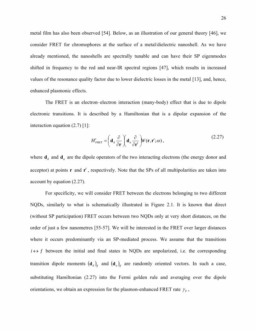
The FRET is an electron–electron interaction (many-body) effect that is due to dipole
electronic transitions. It is described by a Hamiltonian that is a dipolar expansion of the
interaction equation (2.7) [1]:
);,( ωrrr
dr
d ′⎟⎠⎞
⎜⎝⎛
′∂∂
⎟⎠⎞
⎜⎝⎛
∂∂
=′ WH adFRET , (2.27)
where dd and ad are the dipole operators of the two interacting electrons (the energy donor and
acceptor) at points r and r′ , respectively. Note that the SPs of all multipolarities are taken into
account by equation (2.27).
For specificity, we will consider FRET between the electrons belonging to two different
NQDs, similarly to what is schematically illustrated in Figure 2.1. It is known that direct
(without SP participation) FRET occurs between two NQDs only at very short distances, on the
order of just a few nanometres [55-57]. We will be interested in the FRET over larger distances
where it occurs predominantly via an SP-mediated process. We assume that the transitions
fi ↔ between the initial and final states in NQDs are unpolarized, i.e. the corresponding
transition dipole moments ( )ifdd and ( )ifad are randomly oriented vectors. In such a case,
substituting Hamiltonian (2.27) into the Fermi golden rule and averaging over the dipole
orientations, we obtain an expression for the plasmon-enhanced FRET rate Fγ ,

27
( ) ( )JWifaifd
F2
2
22
);,(9
2ω
πγ αβ rr
dd′=
h,
(2.28)
where the dyadic renormalization potential is defined through the renormalized interaction
);,( ωrr ′W [see Eq. (2.7)] as
);,();,(2
ωωβα
αβ rrrr ′′∂∂
∂=′ W
rrW , zyx ,,, =βα ,
(2.29)
and J is the spectral overlap integral.
Another important process, which can contribute to the linewidths of the NQD donor and
acceptor transitions, is the nonradiative transfer of energy from NQDs to a metal. The
corresponding contribution to the linewidths mγ can be found in a straightforward way [26] in
the form
);,(Im32 2
ωε
πγ αβ rr
dG
dm
h−= ,
(2.30)
where d is either or ad , r is the position of the NQD, which is considered as a point-like
object, and the dyadic Green’s function is defined by Eq. (1.42).
Besides the FRET and the energy transfer to the metal (nonradiative relaxation), there is
also the process of the radiative relaxation, which can also be enhanced by the nanoplasmonic
system (nanoantenna effect [26]). The corresponding transition renormalized (SP-enhanced)
dipole rd and the radiative relaxation rate rγ are given by
2
3
3
34
rr cd
h
ωγ = , ∫ ′′′Θ+=V
r rdGddd 3);,()( ωαββαα rrr . (2.31)
where d is the bare transition dipole.
dd

28
We will calculate here the FRET rate Fγ averaged over the position of the acceptor on
the nanoshell with inner and outer radii b and a . Because we are interested in the SP-enhanced
transfer over distances much exceeding the usual Förster range, we disregard the bare Coulomb
potential )( rr ′−V . Then substituting the SP eigenfunctions and eigenvalues [see (2.8), (2.9)]
into (2.28) and integrating over the solid angle of the vector r′ , we obtain [46]
∑∞
=
+
⎟⎟⎠
⎞⎜⎜⎝
⎛′
++=1
42222
622
22
)1)(12(),(9
2
l
l
ld
adF rr
allxFJa
ωε
πγ
h
dd.
(2.32)
The rate of the excitation quenching due to the energy transfer to the metal on the
nanoshell is obtained from (2.30) by the substitution of the SP eigenfunctions and eigenvalues.
This procedure is actually greatly simplified, without affecting the result, if the angular
averaging is performed. This leads to a simple expression [46]
∑∞
=
+
⎟⎠⎞
⎜⎝⎛++−=
1
42
3
2
)1)(12)(,(Im6 l
l
ld
m rallxF
aω
εγ
h
d.
(2.33)
We compute the FRET rate for CdSe NQDs that are situated at the surface of a silver
nanoshell. For certainty, we further assume that they are positioned at the opposite sides of the
nanoshell, as illustrated in Figure 2.4(a). In CdSe NQDs the lowest-energy emitting exciton state
has a relatively weak oscillator strength and is shifted by a few tens of meV (global Stokes shift)
to the red with respect to the stronger absorbing transition (see spectra shown by the bold black
lines in Figure 2.4(a)). Because of this significant Stokes shift, the energy transfer occurs with an
appreciable efficiency only between NQDs with some size differences, which provides resonant
coupling of the emitting state of the donor (the smaller NQD) to the absorbing state of the
acceptor (the larger NQD) [56, 57]. This process is schematically illustrated in Figure 2.4 (a).
mγ

29
Figure 2.4. (color online) Transfer and relaxation rates for NQDs at the outer surface of a silver nanoshell, modified and enhanced by SPs. (a) Schematic of the system and energy transfer processes. A nanoshell is indicated by a blue circle, and the donor and acceptor NQDs are labeled by D and A, correspondingly. The frequency distributions of the transition oscillator strengths of the donor and acceptor NQDs are shown by bold black curves. The energy transfer between NQDs and subsequent relaxation are indicated by red arrows. (b)–(d) The nonradiative and radiative relaxation rates (on logarithmic scale) for NQDs on nanoshells for the aspect ratios specified in the panels. The FRET rate (2.28) for two NQDs situated on the opposite poles of a nanoshell (cf. panel (a)) is shown by the blue curves. The SP-mediated FRET rate averaged over the position of the acceptor on the nanoshell (2.32) is shown by the light-blue curves. The rate of transfer to the metal (2.33) is plotted in green. The radiative rate (2.31) for a NQD at the surface of the nanoshell is depicted by the red curves.
After the Förster energy transfer, indicated by the vertical red arrow, there is a fast (< 1
ps lifetime) relaxation into the lower-frequency state of the acceptor, which precludes energy
transfer back to the donor and allows one to use the perturbation theory result of (2.28)
abx =
Fγ
Fγ mγ
rγ
30
describing an irreversible transfer. We used the adopted NQD parameters for room temperature
condition [56]: 004.0=J cm (or 0.13 ps), 25=ad Debye, and 4.4=dd Debye.
For certainty, we consider a nanoshell with outer radius 20=a nm. The donor and
acceptor NQDs are separated by 2 nm from the metal surface. The FRET rates along with the
rates of the nonradiative and radiative decays of the NQDs are displayed in Figure 2.4(b)–(d).We
show both the FRET rate Fγ (2.28) for the transfer across the diameter of the nanoshell (dark-
blue curves) and the FRET rate (2.32) averaged over the random position of the acceptor on
the surface of the NQD (light-blue curves). This averaged rate is calculated and shown per single
acceptor; if several acceptors participate in the energy transfer, this rate should be multiplied by
the number of such acceptors on the nanoshell. Also shown by the green curves is the rate mγ
(2.33) of nonradiative relaxation due to the energy transfer to the metal. The rate of radiative
decay, rγ , (2.31) is depicted by the red curves.
For all aspect ratios (Figure 2.4(b)–(d)), the FRET rates and are enhanced at the
frequencies of the SP eigenmodes, which is manifested by the corresponding resonant peaks in
the graphs. The number of the efficiently contributing multipoles progressively increases from
two (dipole and quadrupole) for a low aspect ratio (x = 0.1, panel (a)) to very many multipoles
for high aspect ratios (x = 0.85 - 0.95, panels (c) and (d)). With increasing aspect ratio x, the
corresponding FRET rates in these peaks (at the resonant SP frequencies) become higher by
orders of magnitude. This FRET transfer rate is especially large in the lower-frequency spectral
range, which is due to the higher plasmonic quality of the metal.
The energy transfer to metal is an important process because it competes with FRET. The
nonradiative relaxation rate in the donor state of isolated NQDs is low ( -1ns05.0< ); therefore the
Fγ
Fγ Fγ

31
energy transfer rate to metal mγ is the major factor that determines the quantum yield of FRET:
)( FmFFQ γγγ += . We can see from Figure 2.4(b) that for low-aspect ratio nanoshells mF γγ <<
and, hence, 1<<FQ implying that the FRET is inefficient. Low efficiency FRET was also found
for solid nanospheres [53]. As the aspect ratio increases (panels (c) and (d)), this metal-
quenching rate mγ also shows plasmonic peaks; however, it is enhanced significantly less than
the FRET rate. Correspondingly, for x = 0.95 the FRET quantum yield is rather high, 5.0~FQ ,
in the red and near-IR regions of the spectrum. In contrast, the radiative rate rγ (2.31) is orders
of magnitude lower than mγ ; correspondingly, the photoemission quantum yield is very low.
Note that the radiative rate is enhanced only in the odd-multipole (dipole, octupole, etc) SP
resonances due to the parity selection rule.
The overall conclusion from Figure 2.4 is that the SP renormalization of the Coulomb
interaction causes a strong enhancement of the Förster transfer at large distances, across the
entire nanoshell and over a wide range of frequencies where many multipole SP resonances
contribute. This enhancement is especially pronounced for high-aspect ratio nanoshells in the red
and near-IR frequency range where rather high FRET efficiency is predicted.
2.5 General Properties of SP-Renormalized Quasistatic Interaction
To summarize briefly, significant renormalization of the Coulomb interaction between
charged particles (electron, holes, and lattice ions) in the vicinity of a plasmonic nanosystem is
demonstrated for transitions resonant with SP eigenmodes in the nanosystem. There are three
important features of this renormalized interaction that we have shown above and
would like to re-emphasize here. (i) This renormalization (enhancement) is highly resonant. Its
);,( ωrr ′W

32
phase depends on the frequency detuning of the electronic transitions with respect to the SP
resonant frequency, changing by π (from in-phase to out-of-phase and vice versa) as the
frequency ω scans from the red to the blue side of the SP resonance. (ii) The renormalized
interaction is long-ranged: the effective interaction length is on the order of the size
of the entire nanosystem. (iii) This renormalization and plasmonic enhancement of the Coulomb
interaction is a universal effect, which should affect a wide range of physical phenomena in the
vicinity of the metal nanoplasmonic systems: scattering between charge carriers and the carriers
and ions, ion-ion interactions, exciton formation, etc. One of the enhanced and long-range
phenomena, which is due to the nanoplasmonic renormalization of the Coulomb interaction, is
the Förster energy transfer that becomes efficient for high-aspect ratio nanoshells.
Among other potentially very important applications of this theory are chemical reactions
and catalysis on nanostructured metal surfaces. Chemical reactions occur due to the Coulomb
interaction between charged particles (electrons and ions) at small distances. In many cases,
nanostructured metals, in particular noble metal nanostructures with pronounced plasmonic
behavior, are good catalysts. The results of this theory show that the Coulomb interaction at
small distances is significantly renormalized. As we have emphasized in the previous paragraph,
this renormalization is highly resonant, depending on the frequency ω of a transition that
controls the chemical transformation (for example, breaking a chemical bond, establishing a
desired new bond, isomerization, etc). This renormalization leads to suppression of the Coulomb
interaction for the red detunings from the plasmonic resonance. In contrast, this local interaction
is greatly enhanced for blue detunings from the SP resonance. This resonant effect opens up an
avenue toward ‘designer’ nanostructured catalysts that can, e.g., favor one specific reaction path
over others. Another class of important effects, which are based on the nonlocal nature of the
);,( ωrr ′W

33
renormalized Coulomb interaction in the vicinity of a nanoplasmonic system, is the nonlocal
(cross) scattering. A charge at some point can undergo a transition, scattering from a charge at a
remote position, thus ‘teleporting’ momentum and energy. One important instance of such a
remote scattering is a nonlocal SERS where an electronic transition occurs at one point but the
vibrational energy is deposited at a distant point of the nanoplasmonic system.
34
Chapter 3. Electromagnetic Retardation and Surface Plasmon
Polaritons (SPPs)
3.1 Retardation Effects
As was described in Sect. 1.1, if the time variation of electromagnetic field is not fast
enough to overpower the spatial gradients of the field, then the Maxwell equations dramatically
simplify, and electric and magnetic effects can be described separately [1-3, 6]. The formal
condition for this simplification to be valid is given by Eqs. (1.16) and (1.18). Quasistatics is
extremely relevant for nanoplasmonics and has a broad field of applications as was shown in
Chapters 1-2 (see also [22, 26]). Indeed, one of the main goals of nanoplasmonics is to achieve
extremely intense localized fields – the LSPs, which are inherently quasistatic [58]. In contrast,
electromagnetic fields, which are not as intertwined with matter as LSPs (the ideal example
being light in vacuum), do not obey quasistatic approximation. The surface plasmon polaritons
(SPPs) represent an intermediate case between radiation in the vacuum and quasistatic LSPs.
SPP oscillations include coupling to both the magnetic field and collective oscillations of the
solid state electron gas. Retardation effects considered in this Chapter determine the transition
between the two extreme cases of vacuum radiation and LSPs. To incorporate the retardation in
the electrostatic equations (1.1)-(1.2) one needs to restore the coupling to the magnetic field, as
well as to add equations that describe the magnetic field itself. After macroscopic averaging [2, 6]
(see also Sect. 1.1) one obtains the system of macroscopic Maxwell differential equations
35
extπρ4)( =⋅∇ rD , (3.1)
)()( 0 rBrE ik=×∇ , (3.2)
0)( =⋅∇ rB , (3.3)
extcik jrDrB )4()()( 0 π+−=×∇ , (3.4)
where )(0 ck ω= . In the notations adopted in Eqs. (3.1)-(3.4) the charge distributions that bear
no net charge and whose density can be represented by divergence of a vector P⋅−∇=Pρ , are
included in the electric induction PED π4+= . The continuity condition for the motion of these
charges is satisfied automatically by the definition (which is already included into Eq. (3.4))
Pj ωiP −= . (3.5)
The continuity condition for external charges, which lead to the net charge, automatically
follows from Eqs. (3.1) and (3.4).
We do not consider systems with magnetization, whose introduction is problematic at
optical frequencies [6, 59]. Therefore we set HB = , and below these vectors will be used
interchangeably.
The retardation enters into the system (3.1)-(3.4) through the term on the right-hand side
of Eq. (3.2), which leads to circulation of electric field generated by magnetic flux, and through
the displacement current πω 4)(rDj iD −= present in Eq. (3.4).
Consider a homogeneous region with dielectric permittivity ε free from external charges.
Using equations (3.2) and (3.4) one can obtain wave equation for electric field
0)()( 20 =−×∇×∇ rErE εk , (3.6)
and similar one for magnetic field. Since in this case 0)( =⋅∇ rE (see Eq. (3.1)), Eq. (3.6) can be
rewritten as a Helmholtz equation

36
0)()( 20
2 =+∇ rErE εk , (3.7)
leading to dispersion relation for electromagnetic waves within a homogeneous region [2, 6]
ε202 kk = , (3.8)
where k is the wavevector of the electromagnetic wave. Solutions in different regions of
homogeneity should be matched by conditions given by Eqs. (1.9), (1.10), whose form is not
changed by the retardation effects. Other conditions follow from Eqs. (3.3) and (3.4) [2, 6]
0)( =⋅− nBB inout , (3.9)
KBBncinoutπ4)( =−× , (3.10)
where K is the surface current density at the boundary between two regions of homogeneity.
3.2 Radiative Decay of SPs
The properties of LSP resonances depend on the dephasing rate γ (see Sect. 1.2).
Theoretically expression (1.31) becomes invalid for nanoparticles with radii nm25≈≥ slR ,
since it is derived by means of the quasistatic approximation. Besides the quasistatic decay rate
contribution, LSPs on large nanoparticles decay radiatively. The LSP radiative decay has been
investigated in many different metal nanostructures both experimentally and numerically [30, 32,
60]. There is no general analytical representation of LSP radiative lifetime, due to absence of full
electrodynamic spectral theory of LSPs (see Refs. [61, 62]) similar to the quasistatic spectral
theory described in [19] (see Sect. 1.2). This is related to the fact that the problem of
electromagnetic LSP resonances is reminiscent of the quantum mechanical problem of quasi-
discrete states [63], which is not a proper eigenproblem [64]. Despite of this fact, we were able to

37
derive a general expression for the radiative decay rate here for the first time, bypassing these
difficulties.
Let us consider a two-component structure, of the same type as in Sect. 1.2. Let the field
titeet ωγ −−= )(),( 0 rErE be a solution to Maxwell equations (3.1)-(3.4) (with no external charges)
inside some volume V , enclosed by surface S . This field should satisfy the following equations:
0)()()()()( 20
00 =⎟⎟⎠
⎞⎜⎜⎝
⎛ ×∇×∇−Ω−Θ
dks
εrErErEr , )()( 00 rHrE ik=×∇ ,
(3.11)
where complex frequency γω i−=Ω , ck Ω= , [ ] 1)(1)( −−= dms εωεω is the spectral parameter
and )(rΘ is the geometric function, which is equal to 1 in the metal and 0 in the dielectric. From
Eq. (3.11), using vector identities, we obtain
⎟⎟
⎠
⎞
⎜⎜
⎝
⎛⋅×++Ω=Θ ∫∫∫∫
SdVdVV
dSk
idVkk
dVsdV nHEHEEr ˆ)()()( 0*0
202
22
02
0 εε,
(3.12)
where n is a normal ort to the surface S.
From Eq. (3.12) one can obtain an expression for imaginary part of inverse of the spectral
parameter )(1 Ωs to be
⎟⎟
⎠
⎞
⎜⎜
⎝
⎛⋅⎟⎟⎠
⎞⎜⎜⎝
⎛ ×+
Ω−=Θ⎟⎟
⎠
⎞⎜⎜⎝
⎛Ω ∫∫∫
S dVdV
dsk
dVdVs
nHEHEr ˆRe2)()(
1Im 0*02
022
0 εεωγ ,
(3.13)
Acting in the same manner as in (1.28) and neglecting terms on the order of 1−Q for the
dephasing rate we obtain
( )
∫
∫Θ
⋅×
∂∂
+
∂∂
=
V
S
mm
m
dVk
ds
200
0*0
)(
ˆRe
Re
1
Re
)(ImEr
nHE
ωε
ωεωεγ .
(3.14)
38
The first term in Eq. (3.14) represents the quasistatic dephasing [19, 20, 27] (see Eq.
(1.31)), while the second term is the radiative decay rate, which can be also represented in terms
of cycle-averaged quantities as
∫
∫Θ
⋅
∂∂
=
V
S
mr dV
ds
2)(
ˆ4
Re
1Er
nS
ωπ
ωε
γ .
(3.15)
where S is the time-averaged Poynting vector.
Consider a radiative decay of a dipole nanoparticle. The intensity of dipole radiation is
given by [6]
23
2/14
34ˆ dnS
cdsI d
S
εω=⋅= ∫ .
(3.16)
The dipole moment of a small spherical nanoparticle is given by
EEErd 3
34)(
4RVdV dmdmdm εε
πεε
πεε −
=−
≈Θ−
= ∫ . (3.17)
Substituting this into (3.15), combined with the condition for dipole resonance of the
nanoparticle, dm εε 2−= we obtain
32/5
Re
4⎟⎠⎞
⎜⎝⎛
∂∂
=cR
m
dr
ω
ωε
εγ . (3.18)
This result coincides with expression obtained earlier for dipole radiative decay rate using the
pole approximation for quantum polarizability [65]. Note that quasistatic decay rate (the first
term in Eq. (3.14), see also Eq. (1.31)) dominates the LSP dephasing even for radii larger than sl .
For gold the ratio mstr Rk εγγ Im)(4 30≈ comes close to unity at nm70 ≈radR at SP resonance,
while for silver this critical radius is nm25 ≈radR [65].

39
LSP radiative decay is extremely important in plasmonics [30, 32, 60]. Expression (3.15)
describes radiative decay for any solution of Maxwell equations in two-component structures and,
in principle, can serve as a tool in LSP radiative decay engineering.
3.3 SPPs at Planar Surfaces
Consider a metal-dielectric boundary (plane 0=z , metal being in the 0<z half-space)
and a wave with frequency ω incident upon it from the dielectric side with wavevector in the
plane xz and angle of incidence θ . The metal dielectric function is denoted as )(ωεm , while the
dielectric permittivity of the dielectric is dε . The presence of the boundary splits the incident
wave into transmitted and reflected waves [2, 6]. It is important that there are two independent
cases of this separation depending on whether the magnetic field is perpendicular to the plane of
incidence (TM polarization), or the electric field is (TE polarization). We consider the situation
of the TM-polarized incident wave that is more important for us. We will write the magnetic
fields of the waves as
tizikxik eeeHtr zx ωαα
αα −= yH ˆ),( , (3.19)
where tri ,,=α denotes incident, reflected and transmitted fields correspondingly. The problem
is translationally invariant in the xy plane. Therefore, the field dependence on these coordinates
should be the same in both media, which leads to the phase matching condition for all three
waves
θε sin0 dxtxrxix kkkkk ==== , (3.20)
From Eqs. (3.8) and (3.20) it follows that z-components have the form
40
220 xdrziz kkkk −−=−= ε , (3.21)
mxmtz ikkk κωε =−−= 220 )( . (3.22)
Metal dielectric functions in plasmonics, i.e. )(ωεm at frequencies between near-infrared and
visible range, are almost real negative numbers. Therefore, expression (3.22) is almost imaginary
and the field exponentially decays into the metal. The length of this decay is the so-called skin
depth (see Sect. 1.1) given by
θεωεκ
20
sin)(ReRe1
dm
msl+−
==D . (3.23)
The skin depth reaches maximum at normal incidence, where it depends only on the metal
dielectric function (see Eq. (1.17) and Figure 1.1). The skin depth for non-zero incidence angles
differs from the estimate (1.17) by nm31 − (if incidence is from vacuum).
As follows from boundary conditions, the amplitudes of the reflected and transmitted
magnetic fields are connected to that of the incident field through the Fresnel coefficients TMr ,
TMt [6]
iTMitzdizm
tzdizmr HrH
kkkkH =
+−
=εεεε , (3.24)
iTMitzdizm
izmt HtH
kkkH =+
=εε
ε2 , (3.25)
The Fresnel coefficients have a pole which corresponds to the surface resonance
0=+ tzdizm kk εε . (3.26)
The index of refraction 0kkn x= for the surface resonance can be found [6, 25, 26, 66] from
Eqs. (3.21), (3.22) and (3.26) as:

41
dm
dmnεωεεωεω+
=)()()( . (3.27)
Condition (3.26) and the corresponding index of refraction represent a mode that can
sustain itself without energy flux from the incident wave (see Eqs. (3.24) and (3.25)). Moreover,
in the particular configuration we consider here, the incident wave becomes unphysical and
should be excluded, as it is explained below. Instead, the SPP wave should be excited from the
−∞→x side (in the selected notations) of the boundary plane (see the next Section). This mode
is called the surface plasmon polariton (SPP). It is a physically well-defined excitation, if
)(Im)(Re ωω nn >> . This situation normally occurs at the metal-vacuum interface below the
frequency of static surface plasmon 2pSP ωω ≈ , where pω is the metal plasma frequency.
This plasma frequency is on the order of several electronvolts for most metals. Below the plasma
frequency the real part of metal dielectric function is negative 0)](Re[ <ωεm . From this fact and
from Eq. (3.27) follows the condition for SPP existence, given by
dm εωε −≤)](Re[ . (3.28)
The dispersion of metal dielectric permittivity is described very well by the Drude formula
)()(
2
γωωω
εωεi
pbm +−= . (3.29)
where bε is background dielectric permittivity which can be contributed, for example, by
phonons, and γ is the inverse of the electron relaxation time. With the Drude formula taken into
consideration, Eq. (3.28) translates into condition dbp εεωω +≤ .
Substituting Eq. (3.27) into Eqs. (3.21) and (3.22) one obtains the transverse distribution
of the field in an SPP [26]

42
ddm
ddrz iiknkk κ
εωεεε =+
−=−=)(
2
02
0 , (3.30)
mdm
mmtz iiknkk κ
εωεωεωε −=+
−−=−−=)(
)()(2
02
0 , (3.31)
where the decrements mκ and dκ are almost real positive numbers, whose small imaginary parts
come from the metal absorption. The fact that in a SPP wave rzk and tzk are imaginary means
that SPP propagation is restricted to a direction along the metal-dielectric boundary (the x-axis in
our notation) and SPP field decays exponentially away from the boundary. The SPP skin depth is
again determined by as
))(()(ReRe1
20
dmm
mslεωεωε
κ+−
==D . (3.32)
Additionally the penetration length into dielectric is usually defined for SPPs as
))((ReRe1
20
dmd
ddlεωεε
κ+−
==D . (3.33)
While the SPP field is evanescent, or exponentially decays from the boundary, the field
of the incident wave under SPP existence conditions exponentially diverges at large distances
from the boundary. This field does not correspond to any physical incident wave and should be
excluded. Electromagnetic waves propagating toward a metal surface cannot satisfy the phase
matching condition (3.20) with an SPP field on the metal-dielectric boundary. In other words
SPP cannot be excited directly by illuminating a smooth planar metal surface by electromagnetic
radiation, since linear momentum is not conserved in such a process. There are several
conventional ways of SPP excitation that are discussed in the next Section.
mκ
43
3.4 Excitation of SPPs
To excite SPP waves one needs to fulfill both energy and momentum conservation. As
we have shown in the previous Section, SPPs on a planar interface are dark modes and cannot be
excited by, nor can they decay into photons, due to larger momentum of the SPPs at a given
energy. One way to excite an SPP is to use a grating coupler. The excitation is achieved due to
additional momentum coming from a reciprocal lattice vector of the grating, so that the new
wave-vector is ankk ixix π2+=′ , where a is the grating period [67-72]. A grating on the metal
surface was the setting for the first observation of SPPs by Wood [73]. The grating coupling of
SPP to radiation has been first used to experimentally determine the dispersion relation of the
SPPs on a metal-dielectric interface [74]. Periodic perforation of flat surfaces of ideal metals
with grooves or holes allows not only the excitation of SPPs for further propagation along flat
surfaces, but also leads to the appearance of surface electromagnetic waves in perfect conductors.
These mimic (“spoof”) SPPs are much more strongly bound to the surfaces than conventional
SPPs in far-infrared [75-77]. The perforation of metals has been used to enhance the interaction
of subwavelength holes and slits in metal films with SPPs [78-81].
Another well-known method to increase light momentum is by using a dielectric with
permittivity larger than unity. In this case the wavevector is increased by the factor of dε ,
which allows for an SPP excitation by an attenuated total reflection method. This has been
achieved by Otto [82] and by Kretschmann and Raether [83]. Both the Otto and Kretschmann
geometries use dielectric prisms to increase light momentum. In the Otto geometry the prism is
not contacting the metal surface and in the air gap between them evanescent fields are created
through total internal reflection in the prism [84, 85]. These fields excite SPPs on the metal

44
surface. In the Kretschmann geometry the prism contacts a metal film surface directly and SPPs
are excited on the opposite side of the film by the evanescent fields [85, 86].
Similarly SPPs can be excited locally, if the metal boundary is placed near a source of
confined optical near fields that have wave-vector components parallel to the boundary and that
satisfy phase matching conditions with SPPs. Subwavelength apertures, fluorescent molecules or
metallic particles and others can serve as such sources of confined fields [24, 26, 87].
Historically one of the first methods by which SPPs were excited was transmission of
high-energy electrons through metal films [88]. One can observe losses in the spectrum of
transmitted electrons due to SPP excitation. Electron energy loss spectra (EELS) represent a
powerful method to study SPP properties [89].
3.5 SPPs and SPs at Metal Nanowires
It has been shown experimentally that metal nanowires support SPP modes and are able
to guide optical energy over several microns [90, 91]. SPPs in metal nanowires are very
important for modern technology [92]. Besides subwavelength guiding, the small sizes of the
metal nanowires lead to strong coupling between nanowires and individual quantum emitters [93,
94]. Metal nanowires support azimuthally symmetric SPP mode at all wire radii, which allows
gradual concentration of optical energy via such SPPs in adiabatically tapered nanowires [95, 96],
creating extremely strong (up to metal breakdown) and highly localized fields, crucial for
modern technology.
Consider a metal nanowire with radius R and dielectric permittivity embedded
into a dielectric matrix with dielectric constant dε . A propagating SPP with frequency ω creates
surface charge densities both from the metal and dielectric sides of the interface. The charge
)(ωεm

45
density in dielectric or metal is given by )()(21)( ,, Rzmdmd −= ρδσπ
ρ r with corresponding
Fourier components )()()( 0,, qRRJkmdmd σρ =κ , where the wavevector is ρzκ ˆˆ qk += , with z
and ρ being orts of a cylindrical coordinate system. Using the Maxwell equations (3.1)-(3.4) we
obtain expressions for the complex amplitudes of the azimuthally symmetric mode (TM0)
⎪⎪⎩
⎪⎪⎨
⎧
>⎟⎠⎞
⎜⎝⎛ +−
<⎟⎠⎞
⎜⎝⎛ −−
=RiKK
kRIRi
RiIIk
RKRi
ddd
ddd
d
mmm
mmm
m
ρρκρκκκκεσ
ρρκρκκκκεσ
ω
,ˆ)(ˆ)()()(2
,ˆ)(ˆ)()()(2
100
100
ρz
ρzE ,
(3.34)
⎪⎩
⎪⎨
⎧
>
<−=
RKRIRkk
RIRKRkk
dddd
mmmm
ρρκκκσ
ρρκκκσω
,ˆ)()()(2
,ˆ)()()(2
100
100
φ
φH ,
(3.35)
where mm kk εκ 20
2 −= , dd kk εκ 20
2 −= and k is the SPP wavenumber. Complex fields
resulting from (3.34)-(3.35) are proportional to tie ω− .
Matching tangential components of the fields (3.34)-(3.35) leads to the following
relationships
)()()()( 00
2
00
2
RKRIRIRK ddd
ddmm
m
mm κκεκσκκ
εκσ
= , and
)()()()( 1010 RKRIRIRK ddddmmmm κκκσκκκσ =− .
(3.36)
Excluding surface charges from the system (3.36), we arrive at the SPP characteristic equation
)()(
)()(
1
0
1
0
RKRK
RIRI
d
d
d
d
m
m
m
m
κκ
εκ
κκ
εκ
=− . (3.37)
An important SPP property is its energy flux, which is given by the averaged over an SPP
oscillation period Poynting vector:
)Re(84
*]Im[2 HEHES ×=×= − zkeccππ
. (3.38)
Using the expressions for the fields (3.34)-(3.35) which we have obtained for the TM0
SPP mode we calculate the Poynting vector as

46
⎪⎪
⎩
⎪⎪
⎨
⎧
>
<= −
.,)()()(4
,)()()(4
Re8 2
10*0
2
210*
02
]Im[2
RKRIRkk
RIRKRkk
ecS
dddd
d
mmmm
m
zkz
ρρκκκεσ
ρρκκκεσ
π
(3.39)
Expression (3.39) allows a computation of the time averaged flux of SPP energy (input
power) through a plane 0=z as
∫∞
==0
)0(2 zSd zρρπc (3.40)
Computation of (3.40) requires the following facts [49, 97]
[ ] )()( *1
*1 zIzI = , [ ] )()( *
1*
1 zKzK = , (3.41)
( ))()()()()()( 1122 bxIaxbIaxIbxaIba
xdxbxIaxxI pppppp ++ −−
=∫ . (3.42)
Relations (3.41)-(3.42) can be combined to obtain
( )
.]Im[]Re[2
)]()(Im[]Im[]Re[2
)]()(Im[
)()()()()()(
1*
1*
*1
*1
*2*2
*
aaaxIxaaIx
aaaxIxaaIx
xaIaxIaaxIxaaIaa
xdxxaIaxxI
pppp
pppppp
−+
++
==
=−−
=∫
(3.43)
Finally, for the input power (3.40), we have
,22ωσ Rm Rc Θ=c (3.44)
where
.]Im[]Re[2
)]()(Im[)()(Re
)()()()(
]Im[]Re[2)]()(Im[
)()(Re
0*
120*
02
00
0042
42
0*
120*
0
dd
ddddd
ddd
mm
dm
md
mm
mmmmm
mR
RRKRK
RIRk
kRIRKRIRK
RRIRI
RKRk
k
κκκκκ
κκεκκ
κκ
κε
κε
κκκκκ
κκεω
⋅⎥⎦
⎤⎢⎣
⎡+
+⋅⎥
⎦
⎤⎢⎣
⎡=Θ
(3.45
)
The first part of Eq. (3.36) in the form )()()()(
00
002
2
RIRKRIRK
dd
mm
dm
mdmd κκ
κκκεκεσσ = was used to obtain
(3.45).
Now the components of electromagnetic field (3.34), (3.35) in an SPP pulse can be
represented as follows

47
)()ˆ~ˆ~)(( tkziz eEEtA ω
ρ−+′= ρzE , )(ˆ~)( tkzieHtA ω
ϕ−′= φH (3.46)
where gvztt −=′ , gv is the SPP group velocity at the pulse carrier frequency ω , k is the SPP
wave number and functions zE~ , ρE~ and ϕH~ depend only on radius ρ :
⎪⎪
⎩
⎪⎪
⎨
⎧
>Θ
−
<Θ
−
=
RKRKRKRI
kci
RIRKkc
i
E
dmd
mm
Rm
mmm
Rmz
ρρκκκκκ
ε
ρρκκκ
ε
ω
ω
),()()()(2
),()(2
~
000
02
00
2
(3.47)
⎪⎪⎩
⎪⎪⎨
⎧
>Θ
<Θ
−=
RKRKRKRI
c
RIRKc
Edm
d
m
d
m
Rm
m
mmRm
m
ρρκκκκ
κκ
εκ
ρρκκε
κ
ω
ωρ
),()()()(2
),()(2~
100
0
10
(3.48)
⎪⎪⎩
⎪⎪⎨
⎧
>Θ
<Θ
−
=.,ˆ)()(
)()(2
),()(2
~
100
00
100
RKRKRKRI
kk
c
RIRKkk
cH
dmd
m
dm
md
R
m
mmR
m
ρρκκκκ
κεκεκ
ρρκκκ
ω
ωϕ
φ
(3.49)
We select the normalization for the real amplitude )(tA to satisfy the relation
)()(2 ttA c= . Disregarding the group velocity dispersion in Eq. (3.46) is valid for pulses with
duration of tens of femtoseconds and greater, and frequencies not too close to the SP resonance
[98].
Let us consider the limit of extremely thin wires slR << , where sl is the skin depth of the
metal nanowire. To describe this situation consider the limit when dm kkk εε 00 ,>> . In this
case kdm ≈κκ , and the SPP dispersion equation (3.37) can be approximated by
d
m
xKxK
xIxIx
εωεξ )(
)()(
)()()(
0
1
1
0 −== , . (3.50)
One can resolve Eq. (3.50) for the wavevector
kRx =
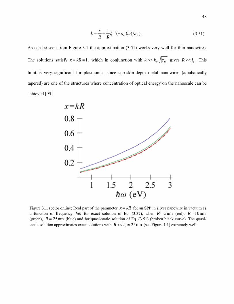
48
))((1 1dmRR
xk εωεξ −== − . (3.51)
As can be seen from Figure 3.1 the approximation (3.51) works very well for thin nanowires.
The solutions satisfy 1≈= kRx , which in conjunction with mkk ε0>> gives slR << . This
limit is very significant for plasmonics since sub-skin-depth metal nanowires (adiabatically
tapered) are one of the structures where concentration of optical energy on the nanoscale can be
achieved [95].
Figure 3.1. (color online) Real part of the parameter for an SPP in silver nanowire in vacuum as a function of frequency for exact solution of Eq. (3.37), when (red), (green), (blue) and for quasi-static solution of Eq. (3.51) (broken black curve). The quasi-static solution approximates exact solutions with (see Figure 1.1) extremely well.
kRx =ωh nm5=R nm10=R
nm25=Rnm25≈<< slR
49
Chapter 4. Forces in Electromagnetic Fields
4.1 Introduction
In 1619 Kepler hypothesized that tails of comets are deflected from the Sun due to
mechanical pressure of solar radiation [26, 99]. Later Maxwell’s theory of electromagnetic
radiation has shown that radiation carries momentum and correspondingly can transfer it to
matter [100]. The numerical value of light pressure due to incident radiation upon a surface,
which is normal to the light propagation direction is given by expression [26]
)1(0 RWp += , (4.1)
where 0W is electromagnetic energy density in the incident wave and R is the reflection
coefficient of the surface. The pressure changes from 0W for a black surface to 02W for an
ideally reflecting surface. The value of this pressure is extremely small, which has made it very
difficult to measure the effect of radiation pressure. Nevertheless, it was first measured in
experiments by Lebedew [101]. Lebedew’s results agreed with the Maxwell’s theory, which was
important evidence in favor of this theory. Lebedew’s studies have also showed there would be
substantial effect of light pressure on macroscopic particles in the interstellar medium, partially
confirming the Kepler hypothesis.
In 1905 Einstein proposed the concept of the photon (“das Lichtquant”) [102] following
the suggestion by Max Plank that energy exchange between light and matter occurs in discrete
quanta [103]. In 1909 Einstein suggested the existence of light pressure fluctuations associated
50
with emission or absorption of quanta with discrete values of momentum [104]. In 1925
Compton experimentally demonstrated the discrete momentum transfer between X-rays and
electrons [105]. In 1933 the deflection of a beam of sodium atoms by the light pressure from a
sodium lamp was observed by Frisch [106]. This deflection was extremely weak, far below the
magnitudes at which it could have any practical application.
The invention of the laser changed the prospects of radiation pressure applications,
creating several huge fields based on momentum transfer from light to matter. The action of laser
radiation upon micron-sized particles and neutral atoms was first investigated in the 1970s in
works of Ashkin [107, 108] and Letokhov [109]. Ashkin and his collaborators have proposed to
trap atomic particles using focused laser beams. Presently such optical tweezers allow trapping
and manipulation of macroscopic particles and even living cells in the range of sizes from 0.1 to
10 micrometers [110-112].
Another important application of light-matter momentum transfer, which became
possible with invention of the laser, is laser cooling [113]. This effect takes place if the radiation
frequency is tuned to the red of an electronic transition in the particles to be cooled. Due to the
Doppler effect, the atoms absorb more photons if they move toward the light source. In a laser
cooling experiment two lasers irradiate particles from opposite directions and particles always
absorb more photons from the source pointing opposite to their direction of motion. Acquiring
more momentum from the direction opposite to the motion of the particle means decreasing the
velocity of the particle. This leads to the cooling effect.
The advent of high-power lasers and appearance of high-power radiation fluxes have
made practical another effect based on light-matter interaction: the photon drag effect. Light
propagating through a semiconductor gets absorbed and transfers its momentum to

51
semiconductor charge carriers. This effect was first observed by Danishevskii et al. [114] and
Gibson et al. [115]. The photon drag effect became of great technical importance for infrared and
terahertz detection of picosecond pulses using semiconductor photon drag detectors [116].
4.2 Electromagnetic Stress-Energy Tensor
For a system with Lagrangian ⎟⎟⎠
⎞⎜⎜⎝
⎛≡
∂∂
Λ ii
qxqq, one can introduce a tensor [1]
Λ−∂Λ∂
=k
ik
i qqT , (4.2)
for which the relationship
0=∂∂
k
ki
xT
(4.3)
is satisfied. Here q is some function of spatial coordinates and time (denoted as ix , with 0=i
for time), which determines the state of the system. Relation (4.3) is equivalent to the statement
that the following vector is conserved
∫= kiki dST
cP 1 ,
(4.4)
where the integration is over a hypersurface containing a three-dimensional space. The vector
given by (4.4) is the 4-momentum of the system, and ikT is the stress-energy tensor. It has to be
symmetric, with kiik TT = .
If we select for integration in (4.4) the hypersurface constx =0 the 4-momentum
assumes the following form
∫= dVTc
P ii 01 , (4.5)

52
where now the integration is over the 3-dimensional space. The space components of iP form
the 3-momentum of the system, while the temporal component is its energy divided by c .
Therefore, the momentum density of the system is given by
( )302010 ,,1 TTTc
=p , (4.6)
and energy density by
00TW = . (4.7)
From Eq. (4.3) it follows that energy flux density, pS 2c= , is connected to momentum density
W. Other components of the tensor form a 3-tensor αβσ− ( zyx ,,, =βα ) of momentum flux
density or the stress tensor with inverse sign.
The electromagnetic Lagrangian [1]
klkl FF
π161
−=Λ , (4.8)
leads to the following expression for electromagnetic stress-energy tensor
⎟⎠⎞
⎜⎝⎛ +−= lm
lmikk
lilik FFgFFT
41
41π
, (4.9)
In expressions (4.8), (4.9) klF is the tensor of electromagnetic field and ikg is the metric tensor.
The electromagnetic 3-dimensional stress tensor, called the Maxwell tensor, can be
expressed in terms of electric and magnetic fields [1-3]
αβ
αββαβααβ
π
δπ
σ
⎟⎠⎞
⎜⎝⎛ +−⊗+⊗=
=⎟⎠⎞
⎜⎝⎛ +−+=
IHHEE ˆ)(21
41
)(21
41
22
22
HE
HEHHEE
(4.10)
where ⊗ denotes outer vector product which gives tensor kiik AB=⊗ )( AB and I is a unity
matrix.

53
4.3 Energy and Momentum Transfer in Electromagnetic Fields
It can be shown that stress-energy tensor is directly connected to energy and momentum
transfer between electromagnetic field and electric charges in this field. Indeed, considerations of
the Maxwell equations (3.1)-(3.4) taken in the temporal domain in the vacuum, i.e. when ED =
and HB = , shows that [1]
EjEjEEHH
EHHEHES
⋅−⎟⎟⎠
⎞⎜⎜⎝
⎛ +∂∂
−=⎥⎦⎤
⎢⎣⎡ ⋅−⋅
∂∂
−⋅∂∂
−=
⋅×∇−⋅×∇=⎥⎦⎤
⎢⎣⎡ ×=
extextHE
tctctcc
cc
ππ
π
ππ
8411
4
)()(4
)(4
divdiv
22
(4.11)
Here )(4
HES ×=πc is the Poynting vector, which is electromagnetic energy flux. The term
Ej ⋅ext is the change of the kinetic energy of the charges in an electromagnetic field, i.e. the
energy transferred from an electromagnetic field to charges, and it is expressed in terms of stress-
energy tensor elements:
⎟⎠⎞
⎜⎝⎛ +∂∂
−=⋅ SEj divt
Wext
(4.12)
Similarly, momentum transfer can be determined from stress-energy tensor elements [26]
( )( )
)(1ˆ)(21
41div
4)(1)(
41
41
22
2
HjEIHHEE
EEEHjEEHH
HEHES
×−−⎥⎦
⎤⎢⎣
⎡⎟⎠⎞
⎜⎝⎛ +−⊗+⊗=
=−⋅∇
+×−××∇+××∇=
=⎟⎠⎞
⎜⎝⎛
∂∂
×+×∂∂
=⎟⎠⎞
⎜⎝⎛
∂∂
extext
extext
cHE
c
ttcct
ρπ
ρππ
π
(4.13)
Here the following identity has been used
[ ] ( ) kcikikiik ABAB IABABBABA ˆ)(div)()()( ⋅−⊗=∂−∂=⋅∇+××∇ , (4.14)
where superscript “c” exempts a vector from differentiation.

54
Eq. (4.13) expresses the change of momentum of external charges in electromagnetic
field, given by the Lorentz force )(1 HjEF ×+= extextext cρ , through the elements of the stress-
energy tensor:
⎥⎦
⎤⎢⎣
⎡⋅∇−⎟
⎠⎞
⎜⎝⎛
∂∂
−= σSF ˆ2ctext (4.15)
Consider, for example, an electromagnetic wave in the vacuum, incident and partially
reflected from some interface. The field in front of the interface has the following form
( )( ) tiikzikz
tiikzikz
ereeE
ereeEω
ω
−−
−−
−=
+=
ReˆReˆ
0
0
yH
xE
(4.16)
The pressure exerted by the wave (4.16) can be computed using Eq. (4.15) as [26]
( )π4
,1ˆˆˆ1ˆ20
02
0EWrWds
Ap
A=+=⋅= ∫ zzσz
(4.17)
where A is an area on the surface parallel to the interface and σ is time averaged stress tensor.
Eq. (4.17) is consistent with Eq. (4.1). The idea behind this example was generalized by Novotny
for compute forces acting on dielectric particles in optical tweezers using expression similar to
(4.17), but with integration over surfaces enclosing corresponding particles [111].
4.4 Forces Acting on a Dipole in an Electromagnetic Field
To better understand the components contributing to force in electromagnetic fields, for
example, in optical tweezers, let us consider the force acting on an electric dipole in an
electromagnetic field. The dipole d is situated at point r . Charges of the dipole experience a
Lorentz force
⎥⎦⎤
⎢⎣⎡ ×+= )(1)()( rBrrErF &
cqq .
(4.18)

55
The resultant force on the dipole is given by
⎟⎟⎠
⎞⎜⎜⎝
⎛++⎟⎟
⎠
⎞⎜⎜⎝
⎛−= − qq qq 22
drFdrFF . (4.19)
Expanding over qd to the first order we obtain [117]
BdrBdEdF )(1)( ∇⋅×+×+∇⋅=cc&&
(4.20)
We drop the last term, since we assume that 1<<cr& . We can rearrange the second term
as follows
)(1)()(111 BdEdBdBdBd ×+×∇×=×+⎟⎠⎞
⎜⎝⎛
∂∂
−×=×dtd
cdtd
ctcc&
(4.21)
Here we used the fact that tdtd ∂∂≈ BB , since . This gives an expression for
the force
)(1)( BdEdF ×+⋅∇=dtd
cc ,
(4.22)
where the following identity was utilized
)()()( BABABA ⋅∇=×∇×+∇⋅ c ; (4.23)
as in Eq. (4.14) the superscript “c” exempts a vector from differentiation.
Let us consider a monochromatic field
titi ee ωω −− == )(Re,)(Re 00 rBBrEE (4.24)
The dipole moment in this field assumes the following form
)()(,Re 00 rEddd ωαω == −C tie , (4.25)
where )(ωα denotes the dipole polarizability.
The time averaged force in field (4.24) is given by
)(Re21 *
00 EdF ⋅∇= (4.26)
1<<cr&

56
Representing the complex amplitude as nE ˆ0Ri
ReE ϕ= , where RE and Rϕ are real, and n
gives the field’s polarization, we get [26]
( ) RRRRRRR EEiEEE ϕααϕα ∇′′
+∇′
=∇−∇= 222
24Re
21F .
(4.27)
where we used the usual notation ααα ′′+′= i . The first term in Eq. (4.27) is the striction (or
gradient) force, while the second one is the pressure force.
Consider a focused laser beam. A small dielectric particle in this beam is acted upon by
two forces, according to (4.27). In the direction of the light beam propagation there is the light
pressure force on the particle, while striction force pulls the particle into the region of high
intensity, i.e. towards the focus. This principle is behind so-called optical tweezers, which allow
control and manipulation in space of tiny particles by focused light beams.
4.5 Radiation Pressure in Macroscopic Bodies and the Photon Drag Effect
It is difficult to derive an expression for the force acting on distributed object similar to
(4.27) (see the next Section), but for the large objects one can neglect the striction force and
consider only pressure, since gradients of the fields are not very large in this case. Pressure force
density can be nicely estimated as follows. The field energy dissipation per unit of time and per
unit of volume Q divided by ωh is the number of absorbed photons. If this quantity is
multiplied by photon momentum kh , we obtain the rate of momentum transfer from radiation to
matter per unit volume, or the pressure force density
22
28EEQ
p kkkf χωπ
εωω
′′=
′′== h
h.
(4.28)
Expression (4.28) is the same as the second term in (4.27) with the imaginary part of the
macroscopic polarizability χ ′′ , instead of the dipole polarizability α ′′ .
57
An extremely important practical application of radiation pressure is the photon drag
effect in semiconductors [115]. Consider a light beam with intensity P in watts propagating
through a semiconductor. The average rate of momentum transfer due to absorption from the
beam to the sample per unit volume is
Ae
cP L αα− ,
(4.29)
where α is the semiconductor absorption coefficient ( 1cm− ), L is the distance into the sample
and A is the cross-section of the sample perpendicular to the beam. This momentum transfer
drive the free carriers along the sample, but in the case of an open circuit it leads to the
emergence of a rectified field E opposing the pressure force. This is the photon drag effect. The
photon drag field at the depth is given by
Ae
cPneE L αα−= ,
(4.30)
where n is electron density. To obtain the total open circuit rectified voltage one should
integrate (4.30) over the whole sample, with the length denoted as 0L [115]:
)1(1
1)1(0
0
RAPR
eRe
AnecRPV HL
L
−≈⋅+
−−−= −
−
α
α
, (4.31)
Here reflection, with coefficient R on both sides of the sample, is taken into account and
)/(1 necRH −= is the Hall constant. The last part of the equation (4.31) is correct if the sample is
long or if absorption is strong, so that 10 >>Lα .
4.6 Macroscopic Force Acting on Polarized Matter
In a recent paper [118] we have derived a general formula describing momentum transfer
between electromagnetic fields and extended polarizable structures. Consider a metal
L

58
nanostructure propagating an SPP pulse. The SPP field produces polarization P , charges with
macroscopic density Pdiv−=ρ , current density t∂∂= Pj , and surface charge density
)( nP ⋅=σ at the surface of the metal, where n is the normal to the surface pointing outward.
We do not consider systems with optical magnetism, whose introduction at optical frequency is
problematic [6, 59]. Therefore , which precludes the existence of surface currents.
Then a macroscopic (averaged) Lorentz force density inside the material volume is given
by
BPPEf ×∂∂
+⋅∇−=tcv
1)( . (4.32)
The surface polarization charges experience the Lorentz force with a surface density
Ef σ=s . (4.33)
Using relation (4.14) the volume force density given by Eq. (4.32) can be represented in
the following way
tc
tcc
cv
∂×∂
+⋅+⊗−=
=×∂∂
+××∇+⋅∇+⊗⋅−∇=
)(1)grad()div(
1)()()(
BPEPEP
BPBEEPEPf,
(4.34)
Thus, the total force acting on the polarization charges in the SPP field is
∫∫ +=S
sV
v dsdV ffF , (4.35)
where the first integration runs over volume V of the structure, and the second is over its surface
S . Noticing that the volume integral of the first term in the last part of Eq. (4.34) is equal to
∫∫∫ −=⋅−=⊗−S
sSV
dsdsdV fEnPEP )()div( , (4.36)
we cancel terms in Eq. (4.35) to simplify it and obtain the following general expression for the
time-averaged total force acting upon the object [118]
HB =
59
dVtcV
c∫ ⎟⎟⎠
⎞⎜⎜⎝
⎛∂×∂
+⋅=)(1)grad(Re
21 *
* BPEPF , (4.37)
Note that we calculate macroscopic forces assuming that the nanostructure is homogeneous
enough and the frequencies under consideration are far enough from the surface plasmon (SP)
resonances. Then the field fluctuations, characteristic of the disordered systems [4], can be
disregarded.
The result (4.37) is of fundamental importance for processes involving interaction of
nanoplasmonic fields with metal electrons. Equation (4.37) is similar to the force acting on a
point dipole moment (see Eq. (4.22) and Ref. [117]), but is more general. It is valid for a wide
range of problems with a general material equation EP χ= , including those where operator χ
describes anisotropic or non-local media. The first term in Eq. (4.37) includes the pressure and
gradient (striction) forces similarly to Eq. (4.27), which is extremely important for
nanotechnology, since the gradient (striction) force becomes large on the nanoscale (see Chapter
5). The second term in Eq. (4.37) is known as the Abraham force. In a monochromatic field, this
force averaged over the period of oscillations is zero, but in the field of a pulsed excitation it has
a finite magnitude.

60
Chapter 5. Giant Surface Plasmon-Induced Drag Effect (SPIDEr)
5.1 Introduction
The fact that electromagnetic fields exert mechanical forces on matter is well known and
has found applications in atomic physics [109, 113] and bio- and nanotechnology [110, 111,
119], and picosecond photodetectors based on the photon drag effect (PDE) [116]. The
semiconductor PDE detectors have proved to be very practical for relatively fast detection of
picosecond pulses in a wide frequency range spanning from THz to infrared. It has been
proposed to use enhanced fields in phonon-polariton silicon carbide structures for laser particle
accelerators [120]. There have been experimental investigations of the PDE in metal nanofilms
that are thicker than the skin depth [121, 122]. Metals support surface plasmon polaritons (SPPs)
[66] that exert forces on electrons causing an SPP-enhanced PDE [121]. However, the PDE is
typically rather small, with the induced potential differences in the mV range. This modest
enhancement of the PDE in these experiments was due to relatively slow variation of SPP fields
in space, and the momentum transferred to the electrons was correspondingly small. Because of
the long relaxation times of the SPPs at plane metal surfaces, this PDE is also expected to be
relatively slow. A drag effect under the conditions of strong nanoplasmonic confinement, when
the SPP localization radius is less than the skin depth ( 25 nm), has not been studied or
exploited theoretically or experimentally.
In the paper [118] we have proposed a giant surface plasmon induced drag effect
(SPIDEr) in metal nanowires which is fast, with a response on the femtosecond time scale. We

61
show that the ultrashort, nanolocalized SPP pulses exert forces on electrons in the nanowires,
inducing giant THz electromotive force (emf) along the SPP propagation direction [see
schematic in Figure 5.1].
Figure 5.1. (color online) Schematic of a SPIDEr in metal nanowire. Propagating SPPs create forces acting on carriers in the nanowire, which leads to THz-band voltage (emf) between the ends of the wire. Picosecond or femtosecond pulses can be used to manipulate the time dependence of the created emf.
We have found that in thin ( 5 nm radius) wires this emf can reach 10 V, with nanolocalized
THz fields as high as 1 MV/cm. Such THz field have previouisly been generated in the far
zone [123], where they produce non-perturbative effects [124], but not on the nanoscale. In
contrast, the plasmonic metal nanowires can serve as nanolocalized sources of high THz fields.
We also study the dynamics of the SPIDEr for short SPP pulses and suggest that thin metal
nanowires can be used as broadband nanoscopic photodetectors with extremely fast response due
to the femtosecond momentum relaxation times in metals. The nature of the giant enhancement
of the SPIDEr is novel in nanoplasmonics: it is not the enhancement of the optical fields per se
(the maximum magnitude of the local fields is limited by the breakdown at the metal surface that
occurs for fields ~ 1 V/Å) but the very high gradients of these fields. The SPIDEr is ultrafast

62
because it is a non-resonant effect whose bandwidth is comparable to that of the entire optical
spectrum.
5.2 SPIDEr in Metal Nanowires
We apply the general Eq. (4.37) to describe the SPIDEr. To be specific, consider a metal
nanowire with radius and dielectric susceptibility )(ωχ , which is oriented along the z-axis
and embedded in a dielectric with a dielectric permittivity of dε . This wire propagates an SPP
pulse, which can be excited by external sources using, e.g., the effect of adiabatic compression
[95, 96].
In the case of extreme nanoplasmonic confinement ( slR << , where sl is the skin depth),
R becomes the only relevant quantity of the dimensionality of length [95]. Therefore there is
scaling of all magnitudes in . The SPP wave power c scales as gvRE 22~c , where
Rvg ω~ is the SPP group velocity. The SPIDEr-induced potential difference [electromotive
force (emf)] X is proportional to the pressure produced by the force from (4.37), 2~ EFX .
The propagation length of the SPP, RQlp ~ , where Q is the SPP figure of merit, independent of
R . These arguments allow us to predict scaling of the SPIDEr force F , emf X , and the electric
field due to SPIDEr rectification RE (which for femtosecond SPP pulses possesses THz
frequencies): 1−∝ RF c , 3−∝ R cX , 4−∝ RER c , 1−∝ REmR . We have also indicated the
scaling of the maximum rectified field mRE (at the maximum tolerable power c ). The scaling
implies that all the effects caused by the SPIDEr increase with decrease in the wire radius as its
powers. This enhancement is not resonant and therefore has bandwidth comparable to that of the
entire optical spectrum. The scaling describes only the dependence on R . There are also
R
R
63
prefactors describing the dependence on dielectric permittivities, frequency, etc. They take into
account an additional enhancement close to the SP resonant frequency, which is multiplicative in
magnitude. Below in this chapter we show that this scaling is reproduced by the theory results.
The SPPs are transverse magnetic (TM) modes, and their complex fields have the form
(see Sect. 3.5)
, (5.1)
where , is the SPP group velocity at the pulse carrier frequency , an k is the
SPP wave number. The total power flowing through the plane 0=z at the moment t is
∫∞
==
0 0),(2)(
zz tSdt rρρπc , where [ ]*Re)8(),( HEr ×= πctSz is the Poynting vector averaged
over the SPP period. Considering the azimuthally symmetric (TM0) modes, the functions ,
and depend only on radius . We normalize them for real amplitude to satisfy a
relation )()(2 ttA c= . Disregarding the group velocity dispersion in Eq. (5.1) is valid for pulses
with duration of tens of femtoseconds and greater, and frequencies not too close to the SP
resonance [98].
The momentum transferred from the electromagnetic field to the electronic system
implies forces exerted on the electrons. The density of these forces is given by Eqs. (4.32) and
(4.33). These forces lead to an emf, which corresponds to optical rectification in the system,
which for femtosecond SPP pulses results in the emf in the THz frequency range. Since the
electron momentum-relaxation time is on the scale of femtoseconds, electrons come to a local
equilibrium in the process of this rectification. Therefore, we will describe it in the
hydrodynamic approximation, for which the pressure p and electrostatic potential φ satisfy an
equation constnep =+ φ , where e is electron charge, and n is electron density. From this
)()ˆ~ˆ~)(( tkziz eEEtA ω
ρ−+′= ρzE )(ˆ~)( tkzieHtA ω
ϕ−′= φH
gvztt −=′ gv ω
zE~
ρE~ ϕH~ ρ )(tA
64
equation, we can find the emf φ∆=X , which is the total change of potential in the direction of
SPP propagation (the z direction), )(nep∆−=X , where )( 2RFp z π=∆ is the full change of
the pressure. Here, zF is z-component of the force (4.37) averaged over the period of SPP
oscillations.
Now let us calculate the force in the fields given by (5.1)
,~)(2
)(2
~)(2
)(
~)(21)()(
~)(2
)()Im(21
)(21)(~Re
21
)(21)()~~~~(Re
21
0
2
0
2
0
222
22
22
2**
ρρχπχπρρχπχπ
ρρχπχπ
χχ
χ
ρρ
dEttQdEttkl
dEez
ttkdzetdzk
dVeEz
ttk
dVez
ttikE
dVez
ttikEPEPF
RR
p
Rzkzk
zk
V
zk
V
zk
Vzzz
∫∫
∫∫∫
∫
∫
∫
⋅⎟⎠⎞
⎜⎝⎛ ′
−′′
=⋅⎟⎠⎞
⎜⎝⎛ ′
′−′′′=
=⋅⎟⎟⎠
⎞⎜⎜⎝
⎛⋅
⎭⎬⎫
⎩⎨⎧
∂′∂
+′′′⋅′+′⋅′′′=
=⋅⎭⎬⎫
⎩⎨⎧
∂′∂′
+′⋅=
=⋅⋅⎭⎬⎫
⎩⎨⎧
∂′∂
+′−⋅=
=⋅⋅⎭⎬⎫
⎩⎨⎧
∂′∂
+′−⋅+=
′′−′′−
′′−
′′−
′′−
cYcY
ccc
cc
cc
cc
(5.2)
where the integration was accomplished in the following way
( ) ,2
)()(21
)(21))((
21)(
)(21)(
0
2
222
2
tet
zetdz
zetdzetdzk
ez
ttkdz
z
z
zk
zkzkzk
zk
cc
cc
c
cc
−=⋅′=
=∂
∂′⋅−∂⋅′∂
⋅+⋅′⋅′′=
=⋅⎭⎬⎫
⎩⎨⎧
∂′∂
+′′′⋅
∞=
=
′′−
′′−′′−′′−
′′−
∫∫∫
∫
(5.3)
and a new function was defined via
∫∫∞−
′−−∞
− ′⋅′=′⋅=t
tt
p
ttlz
p
pp
p ettdt
eetdzl
t )()(1)(0
ccY . (5.4)
The total force Astprz fffF ++= is composed of three forces: the SPP pressure,
striction, and the Abraham force, whose z-components are, correspondingly,
zF

65
)(2
tcA
Rfpr
pr Yπ
= , )(2
tcARf
stst c
π= , )(2
2
tLcRf
AA Y ′=
π . (5.5)
In Eq. (5.5), coefficients prA and stA have dimensionality of area, and AL has
dimensionality of length. They are defined as
1
0
22
~2
−
⎟⎟⎠
⎞⎜⎜⎝
⎛ ′′= ∫
R
pr dER
QcA ρρχ , 1
0
22
~2
−
⎟⎟⎠
⎞⎜⎜⎝
⎛ ′−= ∫
R
st dER
cA ρρχ ,
( )1
0
*2
~~Re−
⎟⎟⎠
⎞⎜⎜⎝
⎛= ∫
Rp
A dHERcl
L ρρχ ϕρ ,
(5.6)
where kkQ ImRe= is the SPP figure of merit, 222 ~~~
ρEEE z += , )Im2(1 klp = is the SPP
propagation length, and gpp vlt = is the SPP pulse lifetime.
These three forces result in three terms of the SPIDEr emf [118]
⎟⎟⎠
⎞⎜⎜⎝
⎛ ′++=
AstprH cL
tA
tA
tRt )()()()( ccYX ,
(5.7)
where necRH 1−= is the Hall constant (cf. Eq. (4.31)).
The Abraham force contribution [the third term in Eq. (3)] is small under the condition
10 <<τkclk p , where ck ω=0 , and τ is the pulse duration. This condition is well satisfied for
the parameters used in this paper.
We will consider two limiting cases pertaining to Eq. (5.7): a quasi-monochromatic
regime of long pulses pt>>τ and a regime of short pulses pt<<τ , where pt is the SPP
dissipation time.

66
5.3 SPIDEr as a THz Source
Consider first the quasi-monochromatic regime ( ), where )()( tt cY ≈ (see Eq.
(5.4)). In such a case, the total emf )(tX follows the pulse-envelope time dependence )(tc .
The computations will be made for a silver [13] nanowire embedded in vacuum ( 1=dε ).
For the quasi-monochromatic case, the total emf X as a function of frequency ω and
wire radius R is displayed in Figure 5.2(a). In contrast to the case of dielectric media, in the
present plasmonic case the SPP pressure and striction contributions to the emf have the same
sign since 0<′χ . These two contributions are equal if a condition χχ ′<′′Q is satisfied. The
black solid line represents this condition; to the left of this line the pressure dominates, and to the
right the striction force gives the major contribution to the SPIDEr. This is understandable
because close to the SP resonance of the wire (at ~ 3.7 eV), the gradient of the SPP intensity
increases due to the high loss: the striction force is of a gradient nature, therefore dominating.
Similarly, with the decrease of R , the intensity gradient increases due to the increased
confinement, which also leads to the relative increase of the striction with respect to the pressure
force, as we clearly can see from this and other panels of Figure 5.2. General increase of the
SPIDEr at the SP resonant frequency can be seen as a broad red peak.
Magnitude of the SPIDEr emf relative to the SPP wave power, cX , is illustrated in
Figure 5.2(b) as a function of the wire radius R for a frequency of eV9.2=ω . The SPIDEr
effect is gigantically enhanced for strong nanoplasmonic confinement: by four orders of
magnitude when decreases from 100 to 5 nm at the same SPP power. There is a pronounced
scaling 3−∝ RcX at slR << , in accord with the discussion in the beginning of Sect. 5.2.
pt>>τ
R

67
The spectral dependence of the relative SPIDEr emf, , for a wire of the smallest
radius considered, nm5 =R , is depicted in Figure 5.2(c). For significantly thinner wires,
nonlocal-response effects may become significant, cf. Refs. [8], [9]. Importantly, the magnitude
of the emf in this case is very large, from 0.01 to 10 V per 1 W of the SPP pulse power, in the
entire optical range, with a pronounced resonance at the SP frequency. This large magnitude
shows that the SPIDEr effect can be used for the photodetection on the nanoscale, i.e., in the role
that previously was deemed only available for semiconductors. In this sense, it belongs to the
area of active nanoplasmonics [98].
By nonlinear optics classification, the SPIDEr is an optical second-order nonlinear effect:
the magnitude of the SPIDEr emf X is proportional to the power c of the SPP field.
Therefore, the maximum achievable magnitude of the emf is determined by the maximum c
that the wire can tolerate. This we estimate setting the optical field E at the surface of the wire
equal to 1 V/Å [125, 126]. For fields significantly higher than this, there will be massive
ionization and damage of the metal surface. We plot in Figure 5.2(d) this maximum intensity as a
function of the wire radius for three SPP frequencies. Note a very good scaling, 3Rm ∝c , in the
region slR ≤ of strong nanoplasmonic confinement. These values of the mc in comparison to
the data of Figure 5.2(a)-(c) show that the gigantic values of of the SPIDEr emf V X 10~ are
realistically achievable, which are many orders of magnitude greater than observed previously in
the metal films [121, 122].
One of the most important for applications properties of the giant SPIDEr is the high
local electric field RE generated due to the SPIDEr optical rectification near the metal nanowire.
Such field (averaged over the SPP decay length pl ) can be found as pR lE X= . We display the
cX

68
Figure 5.2. (color online) SPIDEr for quasi-monochromatic SPP pulses: emf and rectified field dependence on the frequency and wire radius . Note the logarithmic scale for the magtnitude of the effect. (a) Dependence of the SPIDEr emf per unit SPP power on wire radius and frequency. The black broken curve indicates the parameters at which SPP pressure is equal to striction. The magnitude of the effect is denoted by the color-coding bar. (b) Dependence of SPIDEr magnitude on wire radius per unit power of the SPP wave (solid red curve). The contributions of the pressure and striction to the total magnitude of SPIDEr are shown by the dashed curves. (c) Dependence of SPIDEr magnitude per unit power on frequency for . (d) Maximum power that a wire can tolerate as a function of wire radius for different frequencies . (e) The maximum SPIDEr
rectified field (for the maximum tolerable power ) as a function of frequency for three wire
radii = 5, 30, and 100 nm. (f) The maximum SPIDEr rectified field (for the maximum tolerable
power ) as a function of the wire radius for frequency .
ωh RcX
XR
cX ω nm5=R
mc R ω
mRE mc
R mRE
mc R eV55.1 =ωh

69
the maximum achievable rectified field mRE (at the propagating SPP power of mc ) in Figure
5.2(e), (f). As we see from panel (e), the spectral dependence of the SPIDEr rectified THz field is
very similar for all wire sizes, but the magnitude of this field is much greater for the 5 nm wire:
V/cm1010~ 65 −mRE . The nanolocalized THz fields of such a magnitude will excite a wealth of
nonlinear THz responses at the nanoscale.
5.4 SPIDEr as a Femtosecond SPP Detector
Now let us consider dynamics of the emf response to SPP pulses that differ in duration τ
with respect to the SPP pulse dissipation time pt . The latter is displayed in Figure 5.3(a) as a
function of the frequency ω . As we can see time pt is in the range from 10 to 150 fs. The
temporal dependencies of the emf in comparison with the power c of the SPP pulses for
various pulse durations are illustrated in Figure 5.3(b)-(d). For a relatively long pulse (
pt>>= ps1 τ ) shown in Figure 5.3(b), the shape of the emf )(tX repeats that of the power
)(tc . This relatively long, picosecond response, nevertheless, corresponds to a 1 THz
bandwidth for this nanowire used as a nanoscale photodetector. Note that the amplitude of the
emf is very large, 10 V.
For a much shorter, fs40 =τ , SPP pulse and the same 5 nm wire, as shown in Figure
5.3(c), there is a small broadening and delay of the voltaic response (emf) with respect to
the excitation SPP pulse . This broadening is due to the pressure force that decays
exponentially for long times, as Eq. (5.4) suggests, and the broken blue line in the figure
indicates. However, under the conditions considered, this delay and broadening are not large.
The frequency-response bandwidth of this wire as an SPP photodetector on the nanoscale is very
)(tX
)(tc

70
large, ~ 20 THz, which is characteristic of the extreme nanoplasmonic confinement. The
amplitude of the SPIDEr emf is also very large, V10~ X .
Figure 5.3. (color online) SPIDEr created by ultrashort SPP pulses: fast femtosecond emf response. (a) The dependence of the SPP lifetime on the frequency for and . (b) The time dependence of the emf (green line, left scale) and input power (red line, right scale). The pulse duration is and the emf closely follows the SPP pulse
dynamics. (c) The same for much shorter pulse with . The pressure-induced emf leads to a small broadening in the emf dynamics (green line). The limiting exponential decay is outlined by the broken blue line. (d) Emf induced by the short pulse in nanowire with with frequency
. The emf response is broadened, since , while .
For a much thicker nanowire of nm30 =R (weak plasmonic confinement case) and
eV2.1 =ωh , illustrated in Fig. 3 (d), the SPP decay time becomes much longer ( fs150 =pt ).
gpp vlt = ωh nm5 =R nm30 =R)(tX )(tc
fs30ps1 ≈>>= pt τfs40 =τ
nm30 =ReV2.1 =ωh fs80 =τ fs150 =pt

71
This leads to a very significant delay and temporal broadening of the emf response with a
pronounced exponential part due to the pressure forces shown by the broken blue line. This
behavior is due to the much longer SPP lifetimes for the weak confinement where a significant
fraction of the SPP energy propagates in the dielectric (vacuum). Nevertheless the emf response
bandwidth is still very large, on the order of 5 THz, and its amplitude is also very large,
V1 X ≥ .
5.5 Conclusion
In conclusion, the ultrafast giant SPIDEr in metal nanowires excited by ultrashort SPP
pulses was predicted in paper [118] to generate a gigantic emf up to 10 V for the SPP waves of
realistic and tolerable amplitudes. The SPIDEr enhancement is mostly nonresonant, due to
nanoplasmonic confinement of the SPP fields, which leads to higher gradients of the fields and
their higher magnitudes. Because of its nonresonant nature, the SPIDEr is an extremely fast
effect: the frequency bandwidth of the generated THz fields is realistically 5-20 THz. Due to the
high longitudinal localization of the SPP waves in the case of the strong nanoplasmonic
confinement, the SPIDEr generates very high local THz electric fields at the metal surface,
V/cm1010~ 65 −RE . Such fields are capable of inducing strongly nonlinear responses,
including dissociation of molecules. Among possible applications of the giant SPIDEr are
rectification and detection of the nanoscale femtosecond optical fields, coupling of the
nanoplasmonic elements to semiconductor devices, nonlinear THz spectroscopy on the nanoscale
of chemical and biological nanoobjects for biomedicine, etc.
72
References
1. Landau, L.D. and E.M. Lifshitz, Theoretical Physics. The Theory of Field. Vol. 2. 1988, Moscow: Nauka.
2. Jackson, J.D., Classical Electrodynamics. 3rd ed. 1998, New York: Wiley.
3. Stratton, J.A., Electromagnetic Theory. 1941, New York and London: McGraw-Hill.
4. Stockman, M.I., L.N. Pandey, L.S. Muratov, and T.F. George, Giant Fluctuations of Local Optical Fields in Fractal Clusters. Physical Review Letters, 1994. 72(15): p. 2486-2489.
5. Stockman, M.I., Giant Attosecond Fluctuations of Local Optical Fields in Disordered Nanostructured Media. Physical Review B, 2000. 62(15): p. 10494-10497.
6. Landau, L.D. and E.M. Lifshitz, Theoretical Physics. Electrodynamics of Continuous Media. Vol. 8. 2005, Moscow: Nauka.
7. Lifshitz, E.M. and L.P. Pitaevskii, Theoretical Physics. Physical Kinetics. Vol. 10. 1979, Moscow: Nauka.
8. Larkin, I.A. and M.I. Stockman, Imperfect Perfect Lens. Nano Letters, 2005. 5(2): p. 339-343.
9. Aizpurua, J. and A. Rivacoba, Nonlocal Effects in the Plasmons of Nanowires and Nanocavities Excited by Fast Electron Beams. Physical Review B, 2008. 78(3): p. 035404-14.
10. Chapuis, P.-O., S. Volz, C. Henkel, K. Joulain, and J.-J. Greffet, Effects of Spatial Dispersion in Near-Field Radiative Heat Transfer between Two Parallel Metallic Surfaces. Physical Review B, 2008. 77(3): p. 035431-9.
11. Fuchs, R. and R.G. Barrera, Dynamical Response of a Dipole near the Surface of a Nonlocal Metal. Physical Review B, 1981. 24(6): p. 2940.
12. Born, M. and E. Wolf, Principles of Optics. 1999, Cambridge: University Press.
13. Johnson, P.B. and R.W. Christy, Optical-Constants of Noble Metals. Physical Review B, 1972. 6(12): p. 4370-4379.
14. Bergman, D.J. and Y. Imry, Critical Behavior of the Complex Dielectric Constant near the Percolation Threshold of a Heterogeneous Material. Physical Review Letters, 1977. 39(19): p. 1222.
15. Bergman, D.J., The Dielectric Constant of a Composite Material-a Problem in Classical Physics. Physics Reports, 1978. 43(9): p. 377-407.

73
16. Stockman, M.I., S.V. Faleev, and D.J. Bergman, Localization Versus Delocalization of Surface Plasmons in Nanosystems: Can One State Have Both Characteristics? Physical Review Letters, 2001. 87(16): p. 167401.
17. Stockman, M.I., S.V. Faleev, and D.J. Bergman, Coherent Control of Femtosecond Energy Localization in Nanosystems. Physical Review Letters, 2002. 88(6): p. 067402.
18. Aeschlimann, M., M. Bauer, D. Bayer, T. Brixner, F.J. Garcia de Abajo, W. Pfeiffer, M. Rohmer, C. Spindler, and F. Steeb, Adaptive Subwavelength Control of Nano-Optical Fields. Nature, 2007. 446(7133): p. 301-304.
19. Stockman, M., Electromagnetic Theory of SERS, in Topics in Applied Physics, eds. K. Kneipp, M. Moskovits, and H. Kneipp. Vol 103. 2006, Berlin Heidelberg New York: Springer.
20. Bergman, D.J. and M.I. Stockman, Surface Plasmon Amplification by Stimulated Emission of Radiation: Quantum Generation of Coherent Surface Plasmons in Nanosystems. Physical Review Letters, 2003. 90(2): p. 027402.
21. Noginov, M.A., G. Zhu, A.M. Belgrave, R. Bakker, V.M. Shalaev, E.E. Narimanov, S. Stout, E. Herz, T. Suteewong, and U. Wiesner, Demonstration of a Spaser-Based Nanolaser. Nature, 2009. 460(7259): p. 1110-1112.
22. Focus on Plasmonics, in New Journal of Physics, S. Bozhevolnyi and F. García-Vidal, Editors. 2008.
23. Willets, K.A. and R.P. Van Duyne, Localized Surface Plasmon Resonance Spectroscopy and Sensing. Annual Review of Physical Chemistry, 2007. 58(1): p. 267-297.
24. Near-Field Optics and Surface Plasmon Polaritons. Topics in Applied Physics, ed. S. Kawata. Vol. 81. 2001, Berlin Heidelberg New York: Springer-Verlag.
25. Maier, S., Plasmonics: Fundamentals and Applications. 2007: Springer.
26. Novotny, L. and B. Hecht, Principles of Nano-Optics. 2006, Cambridge, New York: Cambridge University Press.
27. Bosbach, J., C. Hendrich, F. Stietz, T. Vartanyan, and F. Träger, Ultrafast Dephasing of Surface Plasmon Excitation in Silver Nanoparticles: Influence of Particle Size, Shape, and Chemical Surrounding. Physical Review Letters, 2002. 89(25): p. 257404.
28. Li, J., H. Iu, D.Y. Lei, J.T.K. Wan, J.B. Xu, H.P. Ho, M.Y. Waye, and H.C. Ong, Dependence of Surface Plasmon Lifetimes on the Hole Size in Two-Dimensional Metallic Arrays. Applied Physics Letters, 2009. 94(18): p. 183112-3.
29. Sönnichsen, C., T. Franzl, T. Wilk, G. von Plessen, J. Feldmann, O. Wilson, and P. Mulvaney, Drastic Reduction of Plasmon Damping in Gold Nanorods. Physical Review Letters, 2002. 88(7): p. 077402.

74
30. Little, J.W., T.A. Callcott, T.L. Ferrell, and E.T. Arakawa, Surface-Plasmon Radiation from Ellipsoidal Silver Spheroids. Physical Review B, 1984. 29(4): p. 1606.
31. Dulkeith, E., T. Niedereichholz, T.A. Klar, J. Feldmann, G. von Plessen, D.I. Gittins, K.S. Mayya, and F. Caruso, Plasmon Emission in Photoexcited Gold Nanoparticles. Physical Review B, 2004. 70(20): p. 205424.
32. Kokkinakis, T. and K. Alexopoulos, Observation of Radiative Decay of Surface Plasmons in Small Silver Particles. Physical Review Letters, 1972. 28(25): p. 1632.
33. Fleischmann, M., P.J. Hendra, and A.J. McQuillan, Raman Spectra of Pyridine Adsorbed at a Silver Electrode. Chemical Physics Letters, 1974. 26(2): p. 163-166.
34. Jeanmaire, D.L. and R.P. Van Duyne, Surface Raman Spectroelectrochemistry: Part I. Heterocyclic, Aromatic, and Aliphatic Amines Adsorbed on the Anodized Silver Electrode. Journal of Electroanalytical Chemistry, 1977. 84(1): p. 1-20.
35. Albrecht, M.G. and J.A. Creighton, Anomalously Intense Raman Spectra of Pyridine at a Silver Electrode. Journal of the American Chemical Society, 2002. 99(15): p. 5215-5217.
36. Kneipp, K., Y. Wang, H. Kneipp, L.T. Perelman, I. Itzkan, R.R. Dasari, and M.S. Feld, Single Molecule Detection Using Surface-Enhanced Raman Scattering (SERS). Physical Review Letters, 1997. 78(9): p. 1667.
37. Hartschuh, A., H.N. Pedrosa, L. Novotny, and T.D. Krauss, Simultaneous Fluorescence and Raman Scattering from Single Carbon Nanotubes. Science, 2003. 301(5638): p. 1354-1356.
38. Lakowicz, J.R., Radiative Decay Engineering: Biophysical and Biomedical Applications. Analytical Biochemistry, 2001. 298(1): p. 1-24.
39. Shimizu, K.T., W.K. Woo, B.R. Fisher, H.J. Eisler, and M.G. Bawendi, Surface-Enhanced Emission from Single Semiconductor Nanocrystals. Physical Review Letters, 2002. 89(11): p. 117401.
40. Gerton, J.M., L.A. Wade, G.A. Lessard, Z. Ma, and S.R. Quake, Tip-Enhanced Fluorescence Microscopy at 10 Nanometer Resolution. Physical Review Letters, 2004. 93(18): p. 180801.
41. Kuhn, S., U. Hakanson, L. Rogobete, and V. Sandoghdar, Enhancement of Single-Molecule Fluorescence Using a Gold Nanoparticle as an Optical Nanoantenna. Physical Review Letters, 2006. 97(1): p. 017402-4.
42. Novotny, L. and S.J. Stranick, Near-Field Optical Microscopy and Spectroscopy with Pointed Probes. Annual Review of Physical Chemistry, 2006. 57(1): p. 303-331.

75
43. Dulkeith, E., M. Ringler, T.A. Klar, J. Feldmann, A. Munoz Javier, and W.J. Parak, Gold Nanoparticles Quench Fluorescence by Phase Induced Radiative Rate Suppression. Nano Letters, 2005. 5(4): p. 585-589.
44. Ichimura, T., N. Hayazawa, M. Hashimoto, Y. Inouye, and S. Kawata, Tip-Enhanced Coherent Anti-Stokes Raman Scattering for Vibrational Nanoimaging. Physical Review Letters, 2004. 92(22): p. 220801.
45. Kneipp, J., H. Kneipp, and K. Kneipp, Two-Photon Vibrational Spectroscopy for Biosciences Based on Surface-Enhanced Hyper-Raman Scattering. Proceedings of the National Academy of Sciences, 2006. 103(46): p. 17149-17153.
46. Durach, M., A. Rusina, V.I. Klimov, and M.I. Stockman, Nanoplasmonic Renormalization and Enhancement of Coulomb Interactions. New Journal of Physics, 2008. 10: p. 105011.
47. West, J.L. and N.J. Halas, Engineered Nanomaterials for Biophotonics Applications: Improving Sensing, Imaging, and Therapeutics. Annual Review of Biomedical Engineering, 2003. 5(1): p. 285-292.
48. Achermann, M., M.A. Petruska, S. Kos, D.L. Smith, D.D. Koleske, and V.I. Klimov, Energy-Transfer Pumping of Semiconductor Nanocrystals Using an Epitaxial Quantum Well. Nature, 2004. 429(6992): p. 642-646.
49. Gradstein, I.S. and I.M. Ryzhik, Tables of Integrals, Series and Products. 1963, Moscow: Fizmatgiz.
50. Förster, T., Zwischenmolekulare Energiewanderung und Fluoreszenz. Annalen der Physik, 1948. 437(1-2): p. 55-75.
51. Dexter, D.L., A Theory of Sensitized Luminescence in Solids. The Journal of Chemical Physics, 1953. 21(5): p. 836-850.
52. Hua, X.M., J.I. Gersten, and A. Nitzan, Theory of Energy Transfer between Molecules near Solid State Particles. The Journal of Chemical Physics, 1985. 83(7): p. 3650-3659.
53. Govorov, A.O., J. Lee, and N.A. Kotov, Theory of Plasmon-Enhanced Förster Energy Transfer in Optically-Excited Semiconductor and Metal Nanoparticles. Physical Review B, 2007. 76(12): p. 125308-16.
54. Andrew, P. and W.L. Barnes, Energy Transfer across a Metal Film Mediated by Surface Plasmon Polaritons. Science, 2004. 306(5698): p. 1002-1005.
55. Kagan, C.R., C.B. Murray, M. Nirmal, and M.G. Bawendi, Electronic Energy Transfer in CdSe Quantum Dot Solids. Physical Review Letters, 1996. 76(9): p. 1517.

76
56. Crooker, S.A., J.A. Hollingsworth, S. Tretiak, and V.I. Klimov, Spectrally Resolved Dynamics of Energy Transfer in Quantum-Dot Assemblies: Towards Engineered Energy Flows in Artificial Materials. Physical Review Letters, 2002. 89(18): p. 186802.
57. Achermann, M., M.A. Petruska, S.A. Crooker, and V.I. Klimov, Picosecond Energy Transfer in Quantum Dot Langmuir-Blodgett Nanoassemblies. Journal of Physical Chemistry B, 2003. 107(50): p. 13782-13787.
58. Dai, J., F. Cajko, I. Tsukerman, and M.I. Stockman, Electrodynamic Effects in Plasmonic Nanolenses. Physical Review B, 2008. 77(11): p. 115419.
59. Merlin, R., Metamaterials and the Landau-Lifshitz Permeability Argument: Large Permittivity Begets High-Frequency Magnetism. Proceedings of the National Academy of Sciences of the United States of America, 2009. 106(6): p. 1693-1698.
60. Teperik, T.V., V.V. Popov, and F.J. García de Abajo, Radiative Decay of Plasmons in a Metallic Nanoshell. Physical Review B, 2004. 69(15): p. 155402.
61. Bergman, D.J. and D. Stroud, Theory of Resonances in the Electromagnetic Scattering by Macroscopic Bodies. Physical Review B, 1980. 22(8): p. 3527.
62. Evra, U. and D.J. Bergman. Lifetime of Nanoplasmonic States. in Plasmonics: Nanoimaging, Nanofabrication, and their Applications II. 2006. San Diego: SPIE.
63. Landau, L.D. and E.M. Lifshitz, Theoretical Physics. Quantum Mechanics. Nonrelativistic Theory. Vol. 3. 1989, Moscow: Nauka.
64. Ching, E.S.C., P.T. Leung, A. Maassen van den Brink, W.M. Suen, S.S. Tong, and K. Young, Quasinormal-Mode Expansion for Waves in Open Systems. Reviews of Modern Physics, 1998. 70(4): p. 1545.
65. Stockman, M.I., (Unpublished).
66. Plasmonic Nanoguides and Circuits, ed. S.I. Bozhevolnyi. 2008, Singapore: Pan Stanford Publishing.
67. Moreland, J., A. Adams, and P.K. Hansma, Efficiency of Light Emission from Surface Plasmons. Physical Review B, 1982. 25(4): p. 2297.
68. Hutley, M.C. and D. Maystre, The Total Absorption of Light by a Diffraction Grating. Optics Communications, 1976. 19(3): p. 431-436.
69. Devaux, E., T.W. Ebbesen, J.-C. Weeber, and A. Dereux, Launching and Decoupling Surface Plasmons Via Micro-Gratings. Applied Physics Letters, 2003. 83(24): p. 4936-4938.
77
70. Schröter, U. and D. Heitmann, Grating Couplers for Surface Plasmons Excited on Thin Metal Films in the Kretschmann-Raether Configuration. Physical Review B, 1999. 60(7): p. 4992.
71. Worthing, P.T. and W.L. Barnes, Efficient Coupling of Surface Plasmon Polaritons to Radiation Using a Bi-Grating. Applied Physics Letters, 2001. 79(19): p. 3035-3037.
72. Renger, J., S. Grafstrom, and L.M. Eng, Direct Excitation of Surface Plasmon Polaritons in Nanopatterned Metal Surfaces and Thin Films. Physical Review B, 2007. 76(4): p. 045431-7.
73. Wood, R.W., On a Remarkable Case of Uneven Distribution of Light in a Diffraction Grating Spectrum. Proceedings of the Physical Society of London, 1902. 18(1): p. 269-275.
74. Ritchie, R.H., E.T. Arakawa, J.J. Cowan, and R.N. Hamm, Surface-Plasmon Resonance Effect in Grating Diffraction. Physical Review Letters, 1968. 21(22): p. 1530.
75. Hibbins, A.P., B.R. Evans, and J.R. Sambles, Experimental Verification of Designer Surface Plasmons. Science, 2005. 308(5722): p. 670-672.
76. Pendry, J.B., L. Martin-Moreno, and F.J. Garcia-Vidal, Mimicking Surface Plasmons with Structured Surfaces. Science, 2004. 305(5685): p. 847-848.
77. Garcia-Vidal, F.J., L. Martin-Moreno, and J.B. Pendry, Surfaces with Holes in Them: New Plasmonic Metamaterials. Journal of Optics A: Pure and Applied Optics, 2005(2): p. S97.
78. Martín-Moreno, L., F.J. García-Vidal, H.J. Lezec, K.M. Pellerin, T. Thio, J.B. Pendry, and T.W. Ebbesen, Theory of Extraordinary Optical Transmission through Subwavelength Hole Arrays. Physical Review Letters, 2001. 86(6): p. 1114.
79. Lezec, H.J., A. Degiron, E. Devaux, R.A. Linke, L. Martin-Moreno, F.J. Garcia-Vidal, and T.W. Ebbesen, Beaming Light from a Subwavelength Aperture. Science, 2002. 297(5582): p. 820-822.
80. Lopez-Tejeira, F., S.G. Rodrigo, L. Martin-Moreno, F.J. Garcia-Vidal, E. Devaux, J. Dintinger, T.W. Ebbesen, J.R. Krenn, I.P. Radko, S.I. Bozhevolnyi, M.U. Gonzalez, J.C. Weeber, and A. Dereux, Modulation of Surface Plasmon Coupling-in by One-Dimensional Surface Corrugation. New Journal of Physics, 2008. 10(3): p. 033035.
81. Genet, C. and T.W. Ebbesen, Light in Tiny Holes. Nature, 2007. 445(7123): p. 39-46.
82. Otto, A., Excitation of Nonradiative Surface Plasma Waves in Silver by the Method of Frustrated Total Reflection. Zeitschrift für Physik A Hadrons and Nuclei, 1968. 216(4): p. 398-410.

78
83. Kretschmann, E. and H. Raether, Radiative Decay of Nonradiative Surface Plasmons Excited by Light Zeitschrift fuer Naturforschung, Teil A: Astrophysik, Physik und Physikalische Chemie, 1968. 23(12): p. 2135-6.
84. Lockyear, M.J., A.P. Hibbins, and J.R. Sambles, Microwave Surface-Plasmon-Like Modes on Thin Metamaterials. Physical Review Letters, 2009. 102(7): p. 073901-4.
85. Charbonneau, R. and P. Berini, Broadside Coupling to Long-Range Surface Plasmons in Metal Stripes Using Prisms, Particles, and an Atomic Force Microscope Probe. Review of Scientific Instruments, 2008. 79(7): p. 073106-9.
86. Krenn, J.R. and J.C. Weeber, Surface Plasmon Polaritons in Metal Stripes and Wires. Philosophical Transactions: Mathematical, Physical and Engineering Sciences, 2004. 362(1817): p. 739-756.
87. Knight, M.W., N.K. Grady, R. Bardhan, F. Hao, P. Nordlander, and N.J. Halas, Nanoparticle-Mediated Coupling of Light into a Nanowire. Nano Letters, 2007. 7(8): p. 2346-2350.
88. Ritchie, R.H., Plasma Losses by Fast Electrons in Thin Films. Physical Review, 1957. 106(5): p. 874.
89. Cai, W., R. Sainidou, J. Xu, A. Polman, and F.J. García de Abajo, Efficient Generation of Propagating Plasmons by Electron Beams. Nano Letters, 2009. 9(3): p. 1176-1181.
90. Dickson, R.M. and L.A. Lyon, Unidirectional Plasmon Propagation in Metallic Nanowires. The Journal of Physical Chemistry B, 2000. 104(26): p. 6095-6098.
91. Ditlbacher, H., A. Hohenau, D. Wagner, U. Kreibig, M. Rogers, F. Hofer, F.R. Aussenegg, and J.R. Krenn, Silver Nanowires as Surface Plasmon Resonators. Physical Review Letters, 2005. 95(25): p. 257403.
92. Leosson, K., T. Nikolajsen, A. Boltasseva, and S.I. Bozhevolnyi, Long-Range Surface Plasmon Polariton Nanowire Waveguides for Device Applications. Optics Express, 2006. 14(1): p. 314-319.
93. Chang, D.E., A.S. Sorensen, P.R. Hemmer, and M.D. Lukin, Quantum Optics with Surface Plasmons. Physical Review Letters, 2006. 97(5): p. 053002-4.
94. Akimov, A.V., A. Mukherjee, C.L. Yu, D.E. Chang, A.S. Zibrov, P.R. Hemmer, H. Park, and M.D. Lukin, Generation of Single Optical Plasmons in Metallic Nanowires Coupled to Quantum Dots. Nature, 2007. 450(7168): p. 402-406.
95. Stockman, M.I., Nanofocusing of Optical Energy in Tapered Plasmonic Waveguides. Physical Review Letters, 2004. 93(13): p. 137404.
96. Verhagen, E., M. Spasenovic, A. Polman, and L. Kuipers, Nanowire Plasmon Excitation by Adiabatic Mode Transformation. Physical Review Letters, 2009. 102(20): p. 203904-4.

79
97. The Wolfram Functions Site. Available from: http://functions.wolfram.com/.
98. MacDonald, K.F., Z.L. Samson, M.I. Stockman, and N.I. Zheludev, Ultrafast Active Plasmonics. Nat Photon, 2009. 3(1): p. 55-58.
99. Minogin, V.G. and V.S. Letokhov, Laser Light Pressure on Atoms. 1986, Moscow: Nauka.
100. Maxwell, J.C., A Treatise on Electricity and Magnetism. 1873, Claredon Press.
101. Lebedew, P., Untersuchungen über die Druckkräfte des Lichtes. Annalen der Physik, 1901. 311(11): p. 433-458.
102. Einstein, A., Über Einen die Erzeugung und Verwandlung des Lichtes betreffenden heuristischen Gesichtspunkt. Annalen der Physik, 1905. 322(6): p. 132-148.
103. Planck, M., Über das Gesetz der Energieverteilung im Normalspectrum. Annalen der Physik, 1901. 309(3): p. 553-563.
104. Einstein, A. and W. Ritz, Zum gegenwärtigen Stand des Strahlungsproblems. Physikalische Zeitschrift, 1909. 10: p. 185-193.
105. Compton, A.H., The Corpuscular Properties of Light. Naturwissenschaften, 1929. 17(26): p. 507-515.
106. Frisch, R., Experimenteller Nachweis des Einsteinschen Strahlungsrückstoßes. Zeitschrift für Physik A Hadrons and Nuclei, 1933. 86(1): p. 42-48.
107. Ashkin, A., Acceleration and Trapping of Particles by Radiation Pressure. Physical Review Letters, 1970. 24(4): p. 156.
108. Ashkin, A., Trapping of Atoms by Resonance Radiation Pressure. Physical Review Letters, 1978. 40(12): p. 729.
109. Letokhov, V.S., V.G. Minogin, and B.D. Pavlik, Cooling and Capture of Atoms and Molecules by a Resonant Light Field. Soviet Physics - JETP, 1977. 45(4): p. 698-705.
110. Ashkin, A. and J.M. Dziedzic, Optical Trapping and Manipulation of Viruses and Bacteria. Science, 1987. 235(4795): p. 1517-1520.
111. Novotny, L., R.X. Bian, and X.S. Xie, Theory of Nanometric Optical Tweezers. Physical Review Letters, 1997. 79(4): p. 645.
112. Righini, M., G. Volpe, C. Girard, D. Petrov, and R. Quidant, Surface Plasmon Optical Tweezers: Tunable Optical Manipulation in the Femtonewton Range. Physical Review Letters, 2008. 100(18): p. 186804-4.
113. Hänsch, T.W. and A.L. Schawlow, Cooling of Gases by Laser Radiation. Optics Communications, 1975. 13(1): p. 68-69.

80
114. Danishevskii, A.M., A.A. Kastalskii, S.M. Ryvkin, and I.D. Yaroshetskii, Dragging of Free Carriers by Photons in Direct Interband Transitions in Semiconductors. Sov. Phys. JETP, 1970. 31: p. 292.
115. Gibson, A.F., M.F. Kimmitt, and A.C. Walker, Photon Drag in Germanium. Applied Physics Letters, 1970. 17(2): p. 75-77.
116. Ganichev, S. and W. Prettl, Intense Terahertz Excitation of Semiconductors. 2006, Oxford, New York: Oxford University Press.
117. Shimizu, Y. and H. Sasada, Mechanical Force in Laser Cooling and Trapping. American Journal of Physics, 1998. 66(11): p. 960-967.
118. Durach, M., A. Rusina, and M.I. Stockman, Giant Surface-Plasmon-Induced Drag Effect in Metal Nanowires. Physical Review Letters, 2009. 103(18): p. 186801-4.
119. Volpe, G., R. Quidant, G. Badenes, and D. Petrov, Surface Plasmon Radiation Forces. Physical Review Letters, 2006. 96(23): p. 238101-4.
120. Kalmykov, S., O. Polomarov, D. Korobkin, J. Otwinowski, J. Power, and G. Shvets, Novel Techniques of Laser Acceleration: From Structures to Plasmas. Royal Society of London Transactions Series A, 2006. 364: p. 725.
121. Vengurlekar, A.S. and T. Ishihara, Surface Plasmon Enhanced Photon Drag in Metal Films. Applied Physics Letters, 2005. 87(9): p. 091118-3.
122. Hatano, T., B. Nishikawa, M. Iwanaga, and T. Ishihara, Optical Rectification Effect in 1d Metallic Photonic Crystal Slabs with Asymmetric Unit Cell. Optics Express, 2008. 16(11): p. 8236-8241.
123. Sell, A., A. Leitenstorfer, and R. Huber, Phase-Locked Generation and Field-Resolved Detection of Widely Tunable Terahertz Pulses with Amplitudes Exceeding 100 MV/cm. Optics Letters, 2008. 33(23): p. 2767-2769.
124. Leinss, S., T. Kampfrath, K. v.Volkmann, M. Wolf, J.T. Steiner, M. Kira, S.W. Koch, A. Leitenstorfer, and R. Huber, Terahertz Coherent Control of Optically Dark Paraexcitons in Cu2O. Physical Review Letters, 2008. 101(24): p. 246401-4.
125. Gault, B., F. Vurpillot, A. Bostel, A. Menand, and B. Deconihout, Estimation of the Tip Field Enhancement on a Field Emitter under Laser Illumination. Applied Physics Letters, 2005. 86(9): p. 094101-3.
126. Sha, G., A. Cerezo, and G.D.W. Smith, Field Evaporation Behavior During Irradiation with Picosecond Laser Pulses. Applied Physics Letters, 2008. 92(4): p. 043503-3.